Kingston KVR26S19S8-8 User Manual

Memory Module Specifi cations
KVR26S19S8/8
8GB 1Rx8 1G x 64-Bit PC4-2666
CL19 260-Pin SODIMM
DESCRIPTION
This document describes ValueRAM's KVR26S19S8/8
is a 1G x 64-bit (8GB) DDR4-2666 CL19 SDRAM (Synchronous
DRAM), 1Rx8, non-ECC, memory module, based on eight 1G x
8-bit FBGA components. The SPD is programmed to JEDEC
standard latency DDR4-2666 timing of 19-19-19 at 1.2V. This
260-pin DIMM uses gold contact fingers. The electrical and
mechanical specifications are as follows:
FEATURES
• Power Supply: VDD = 1.2V Typical
• VDDQ = 1.2V Typical
• VPP = 2.5V Typical
• VDDSPD = 2.2V to 3.6V
• Nominal and dynamic on-die termination (ODT) for
data, strobe, and mask signals
• Low-power auto self refresh (LPASR)
• Data bus inversion (DBI) for data bus
• On-die VREFDQ generation and calibration
SPECIFICATIONS
CL(IDD)
Row Cycle Time (tRCmin)
Refresh to Active/Refresh
Command Time (tRFCmin)
Row Active Time (tRASmin)
Maximum Operating Power
UL Rating
Operating Temperature
Storage Temperature
*Power will vary depending on the SDRAM used.
19 cycles
45.75ns(min.)
350ns(min.)
32ns(min.)
TBD W*
94 V - 0
o
C to +85o C
0
o
C to +100o C
-55
• Single-rank
• On-board I2 serial presence-detect (SPD) EEPROM
• 16 internal banks; 4 groups of 4 banks each
• Fixed burst chop (BC) of 4 and burst length (BL) of 8
via the mode register set (MRS)
• Selectable BC4 or BL8 on-the-fly (OTF)
• Fly-by topology
• Terminated control command and address bus
• PCB: Height 1.18” (30.00mm)
• RoHS Compliant and Halogen-Free
kingston.com
Continued >>
Document No. VALUERAM1605A 05/03/18 Page 1

continued HyperX
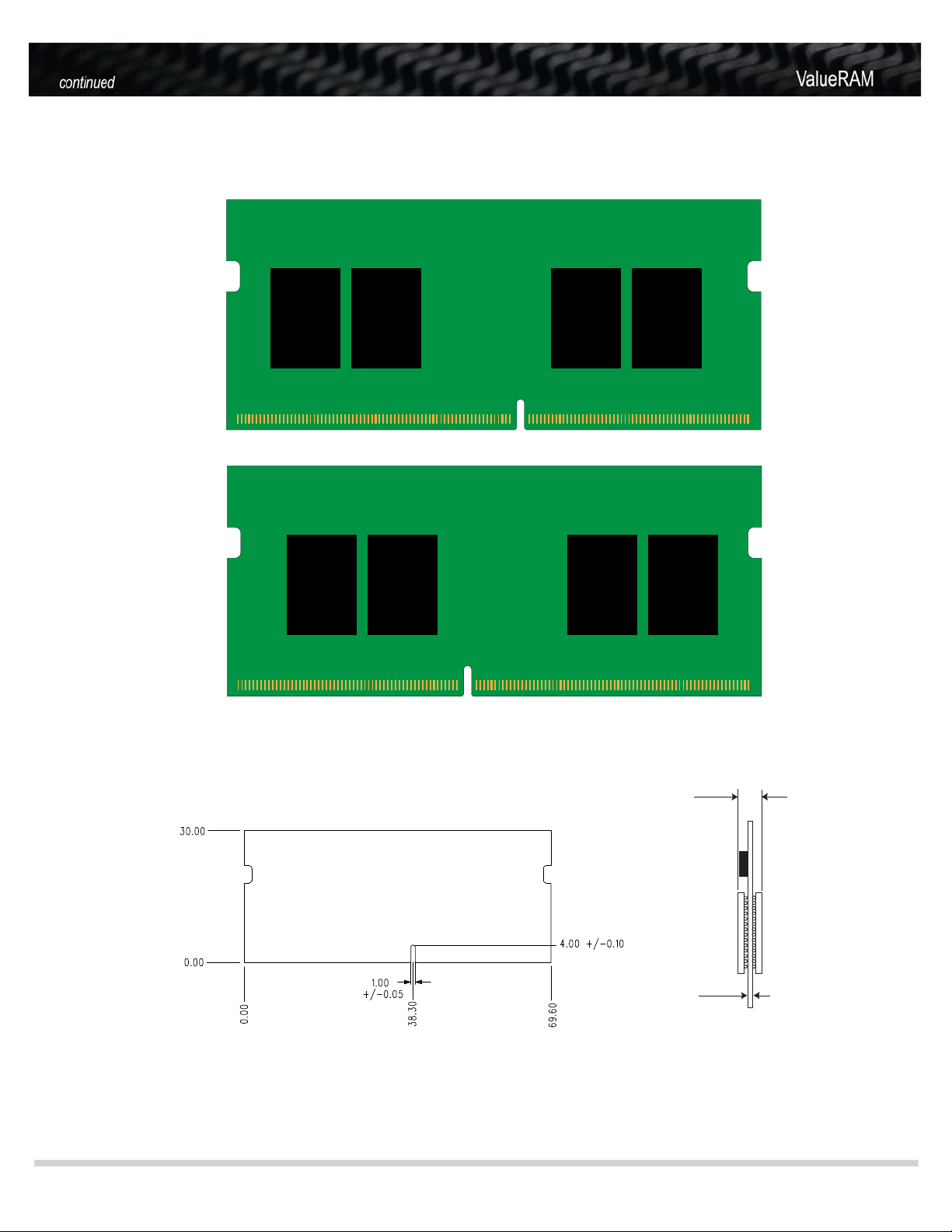
MODULE DIMENSIONS
All measurements are in millimeters.
(Tolerances on all dimensions are ±0.12 unless otherwise specified)
The product images shown are for illustration purposes only and may not be an exact representation of the product.
Kingston reserves the right to change any information at anytime without notice.
kingston.com
©2017 Kingston Technology Corporation, 17600 Newhope Street, Fountain Valley, CA 92708 USA.
All rights reserved. All trademarks and registered trademarks are the property of their respective owners.
3.7 Max
1.20
Side
Document No. VALUERAM1605A Page 2
 Loading...