

Page 1

Memory Module Specifi cations
KSM29RD4/32MEI
32GB 2Rx4 4G x 72-Bit PC4-2933
CL21 Registered w/Parity 288-Pin DIMM
DESCRIPTION
Kingston's KSM29RD4/32MEI is a 4G x 72-bit (32GB)
DDR4-2933 CL21 SDRAM (Synchronous DRAM) registered w/
parity, 2Rx4, ECC, memory module, based on thirty-six 2G x
4-bit FBGA components. The SPD is programmed to JEDEC
standard latency DDR4-2933 timing of 21-21-21 at 1.2V. Each
288-pin DIMM uses gold contact fingers. The electrical and
mechanical specifications are as follows:
FEATURES
• Power Supply: VDD = 1.2V
• VDDQ = 1.2V
• VPP = 2.5V
• VDDSPD = 2.25V to 2.75V
• Functionality and operations comply with the DDR4 SDRAM datasheet
• 16 internal banks
• Bank Grouping is applied, and CAS to CAS latency (tCCD_L, tCCD_S) for
the banks in the same or different bank group accesses are available
• Data transfer rates: PC4-2933, PC4-2666, PC4-2400, PC4-2133, PC4-1866, PC4-1600
• Bi-Directional Differential Data Strobe
• 8 bit pre-fetch
• Burst Length (BL) switch on-the-fly BL8 or BC4(Burst Chop)
• Supports ECC error correction and detection
• On-Die Termination (ODT)
• Temperature sensor with integrated SPD
• This product is in compliance with the RoHS directive.
• Per DRAM Addressability is supported
• Internal Vref DQ level generation is available
• Write CRC is supported at all speed grades
• CA parity (Command/Address Parity) mode is supported
SPECIFICATIONS
CL(IDD)
Row Cycle Time (tRCmin)
Refresh to Active/Refresh
Command Time (tRFCmin)
Row Active Time (tRASmin)
Maximum Operating Power
UL Rating
Operating Temperature
Storage Temperature
* See IDD Table (page2)
Module Assembly
DRAM: MICRON (E-DIE)
RCD: IDT
21 cycles
45.75ns(min.)
350ns(min.)
32ns(min.)
*
94 V - 0
o
C to +85o C
0
o
C to +100o C
-55
kingston.com
Continued >>
Document No. 4808905A 09/24/18 Page 1
Page 2
continued
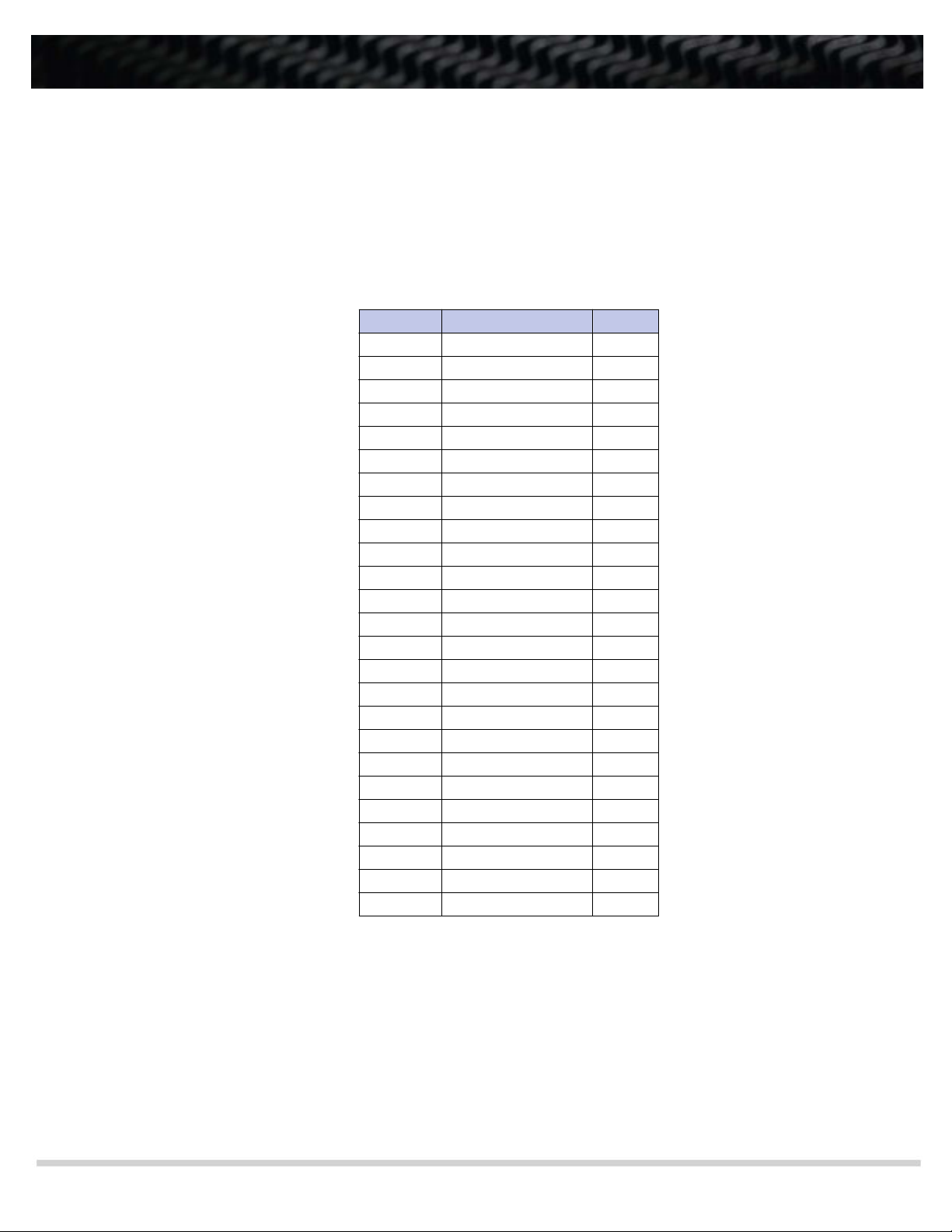
IDD Specifications
Symbol 2933 Units
1
I
DD0
1
I
PP0
1
I
DD1
2
I
DD2N
1
I
DD2NT
2
I
DD2P
2
I
DD2Q
2
I
DD3N
2
I
PP3N
2
I
DD3P
1
I
DD4R
1
I
DD4W
1
I
DD5R
1
I
PP5R
2
I
DD6N
2
I
DD6E
2
I
DD6R
2
I
DD6A
2
I
DD6A
2
I
DD6A
2
I
DD6A
2
I
PP6X
1
I
DD7
1
I
PP7
2
I
DD8
1170
108
1404
1152
1152
792
936
1440
108
1116
2952
2610
1278
144
1224
2088
756
309.6
756
1116
2088
180
4266
306
648
mA
mA
mA
mA
mA
mA
mA
mA
mA
mA
mA
mA
mA
mA
mA
mA
mA
mA
mA
mA
mA
mA
mA
mA
mA
kingston.com
Notes: 1. One module rank in the active IDD/PP, the other rank in IDD2P/PP3N.
2. All ranks in this IDD/PP condition.
Document No. 4808905A Page 2
Page 3

continued
MODULE DIMENSIONS
All measurements are in millimeters.
(Tolerances on all dimensions are ±0.12 unless otherwise specified)
The product images shown are for illustration purposes only and may not be an exact representation of the product.
Kingston reserves the right to change any information at anytime without notice.
kingston.com
©2019 Kingston Technology Corporation, 17600 Newhope Street, Fountain Valley, CA 92708 USA.
All rights reserved. All trademarks and registered trademarks are the property of their respective owners.
Document No. 4808905A Page 3
 Loading...