

Page 1
TYPE IV
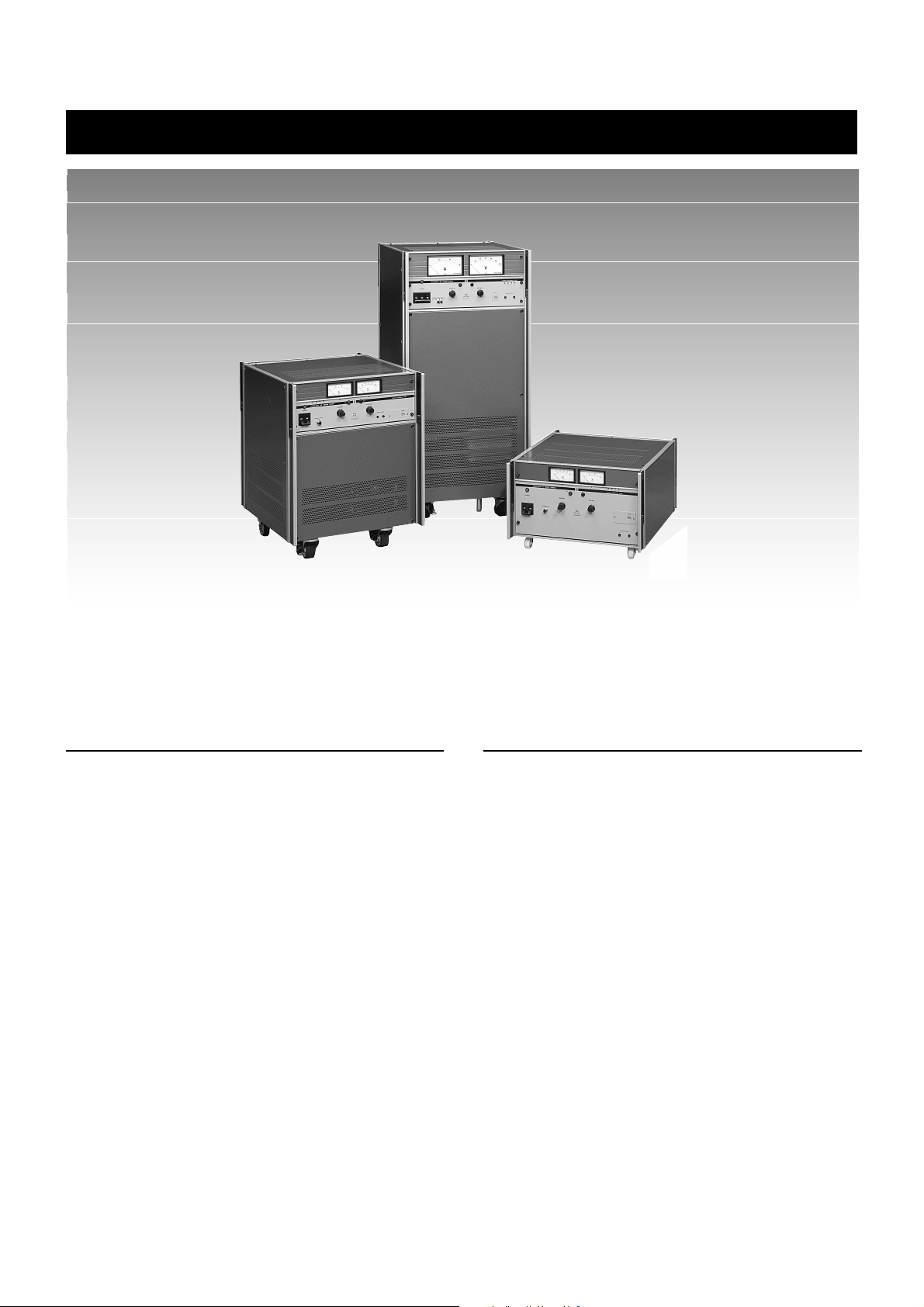
PAD-L/PAD-LP series
REGULATED DC POWER SUPPLY (CV·CC)
TYPE V
TYPE III
High Capacity, Multiple Models, High Performance, High Reliability Power Supply Series
PAD-LP Series Has a Dedicated Ageing Function
Outline
The PAD-L Series are high performance and high reliability
variable DC regulated power supplies used in all fields, from
research and development and quality control to manufacturing plants.
This series is made up of a two excellent regulators: thyristor
preregulator and power transistor series regulator. Therefore,
it combines the high level of performance featured by the series input type with the low power supply harmonic distortion
and efficient output characteristic featured by choke input phase
control.
On the other hand, reliability and safety, which are important
factors in power supply equipment, are ensured by the extensive use of parts that are stringently inspected beginning from
the design stage and mounting know-how accumulated over
many years. All models also have various safety functions,
including an overvoltage protector (OVP).
The “LP” Series is also available which is provided with high
speed OVP function and various status signals suitable for
system use.
Features
■ Improved power factor at low output voltages
Choke input circuit reduces the input apparent current and
improves the power factor.
■ Low AC input voltage waveform distortion
Choke input circuit reduces the harmonic component in the
input current and minimizes line interference.
■ Excellent temperature coefficient
Stringent selection of the parts used, circuit improvements,
and forced-air cooling provide a 50 ppm/˚C low-temperature drift and excellent ageing drift.
■ Fast transient response
Since the wideband differential amplifier has a stable frequency-gain and phase characteristic and a loop gain up to
a high frequency, its output impedance is low and it can
amply respond to sudden changes.
■ Low ripple noise voltage
Both effective value and peak value are low.
■ Various safety functions
Overvoltage protector (OVP), overheating protection circuit, and other highly reliable safety functions are provided.
Page1Copyright © 2002 KIKUSUI ELECTRONICS CORP. All rights reserved. http://www.kikusui.co.jp/
Page 2
PAD-L/PAD-LP series
REGULATED DC POWER SUPPLY (CV·CC)
Two big features of choke input system
■
Low harmonic distortion factor minimizes the affect on other devices
Recently, the problem of harmonic distortion of commercial power
supplies, which are the power source for electric products, has been
closely examined from the sociological standpoint. Harmonic distortion is also said to be a factor in the growth of inverter type rotation control equipment and the popularity of electric devices with a
capacitor input rectifier, which are typified by television sets and
switching regulators. It has also sparked the movement toward restriction of generation of parasitic harmonic currents up to the 40th
harmonic around the world. This flow is different from electromagnetic wave interference (EMI) countermeasures. From the standpoint of other equipment that use the same line, basically there is a
new concept regarding the use of commercial power supplies.
Kikusui has promoted this problem on the same level as efficiency
and electrical characteristics and has taken up suppression (reduction of higher harmonics) of the peak current and improvement of
line distortion by using a choke input system. The choke input type
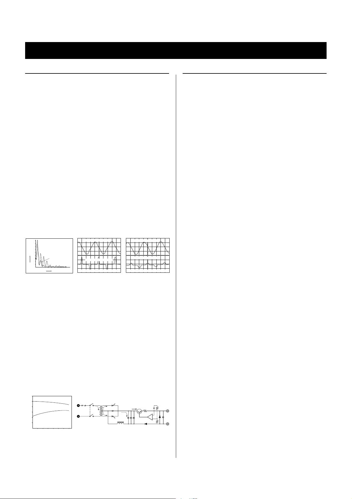
PAD-L/LP Series has a lower harmonic component (Fig. 1) than the
capacitor input system and there is no fear of the resonance phenomena which is generated by the phase-leading capacitor and lead
inductance connected to the same line.
Since the peak value of the charging current is low, the waveform
distortion of the commercial power supply caused by a voltage drop
is also suppressed to a low value (Fig. 2).
180
Higher Harmonic Wave
Fig.1
Amplitude(mV)
Fandamental Wave
160
140
120
100
80
60
40
20
0
3rd Higher Harmonic Wave
50 150 250
Characteristics of the Choke
Input and Capacitor Input
Systems
Capacitor Input System
PAD-L Series (Choke Input System)
5th 7th 9t h 11th 13th 15th 17th 19th
350 450 550 650 750 850 950
Frequency (Hz)
■ Excellent reliability, life, and efficiency. Low input current.
When effective use of energy conservation is considered, the larger
the power supply capacity, the more products with excellent power
supply efficiency are demanded. The chock input system is superior
from this standpoint also.
Since the P AD-L/LP Series is equipped with a choke input type phase
control circuit (preregulator) to reduce the collector loss of the series
control transistor, its full-load current drain is approximately 74%
(Kikusui ratio)of that of the capacitor input system. (Fig. 3)
This is because the “reactive current”, which is a problem with the
conventional capacitor input system, is stored in a choke coil and
reused, and abnormal heating of the power transformer and enlargement of the element due to the tremendous surge on current in the
thyristor are not a problem. There is als no fear of a large ripple cur rent flowing in the electrolytic capacitor which governs the life of
the power supply. (Fig.4)
30
Capacitor Input System
25
20
Choke Input System
15
PAD35-50L
10
5
AC INPUT CURRENT(A)
0
0 5 10 15 20 25 30 35
DC OUTPUT VOLT AC200V 50Hz
Fig.3 Current Consumption Characteristics
O=50A
I
O=50A
I
Input Voltage Waveform
Input Current Waveform
Capacitor Input Type Smoothing Circuit
Fig. 2 Input vpltage-current curves
1
i1T1i2
SCR1
SR1
SCR2
L1
CHOKE COIL
i3
S
F1
AC INPUT
Fig. 5 Basic Circuitry of the PAD-L Series
Input Voltage Waveform
Input Current Waveform
Choke Input Type Smoothing Circuit
SERIES PASS
TRANSISTOR
i4
Eref Ri
ERROR
AMP
ー
+++
C1〜3
+
Rf
SR
2
SR
+
3
Safety functions
Since power supply trouble and accidents caused by erroneous
operation are linked to shutting down of the entire system and
destruction of the expensive load, trouble-free reliability is very
important. The protection circuit for preventing accidents in advance
even if trouble should occur must operate positively in the safety
direction. The P AD-L/LP Series is equipped with the following safety
functions.
■ OverVoltage Protector (OVP)
Protects the load by instantly tripping the power switch circuit protector when erroneous operation or an accident generated an overvoltage. Since the OVP of the LP Series, in particular, is the preset
type, the operating voltage is set by pressing the front panel preset
button while watching the voltmeter. The operation voltage is checked
without interrupting OVP operation even during aging.
• Since the LP Series uses a high-speed thyristor clover type OVP
with a 200µs operation pulse width, use it with semiconductor and
other loads that are especially susceptible to overvoltages.
• The L Series has an operation pulse width of 50ms and protects
the load without erroneous operation by noise.
■ Overheating protection circuit
When the temperature of the main parts inside the equipment rises
above the specified value, this circuit trips the power switch.
■ Voltage detector
When the smoothing electrolytic capacitor voltage rises above the
rated voltage because the rear panel terminal board jumper was not
installed or other mistake or trouble in the rectifier, this circuit immediately trips the rectifier.
■ Surge absorber
Protects the entire power supply against surge voltages generated on
the line by lightning, etc.
■ Fire countermeasures
• The main power transformers uses Class B insulation. The insulation is made of a material that can withstand continuous use without any degradation of its insulating effect even at a high temperature of 130˚C.
• The PC boards are made of incombustible glass epoxy or paper
epoxy.
• The wiring uses heat resistant wire made by irradiating acceleration electron wire.
■ Reverse connection prevention circuit
Protects the power supply even if a reverse polarity voltage is applied to the output terminals.
■ Overcurrent detector
This circuit uses a comparison amplifier to constantly monitor the
output current and prevents the power supply from exceeding its rat-
C
ing due to overinput during remote control and protects the power
supply against overcurrent if the terminal board shorting bar is not
installed by mistake.
Page2Copyright © 2002 KIKUSUI ELECTRONICS CORP. All rights reserved. http://www.kikusui.co.jp/
Page 3
PAD-L/PAD-LP series
REGULATED DC POWER SUPPLY (CV·CC)
Application
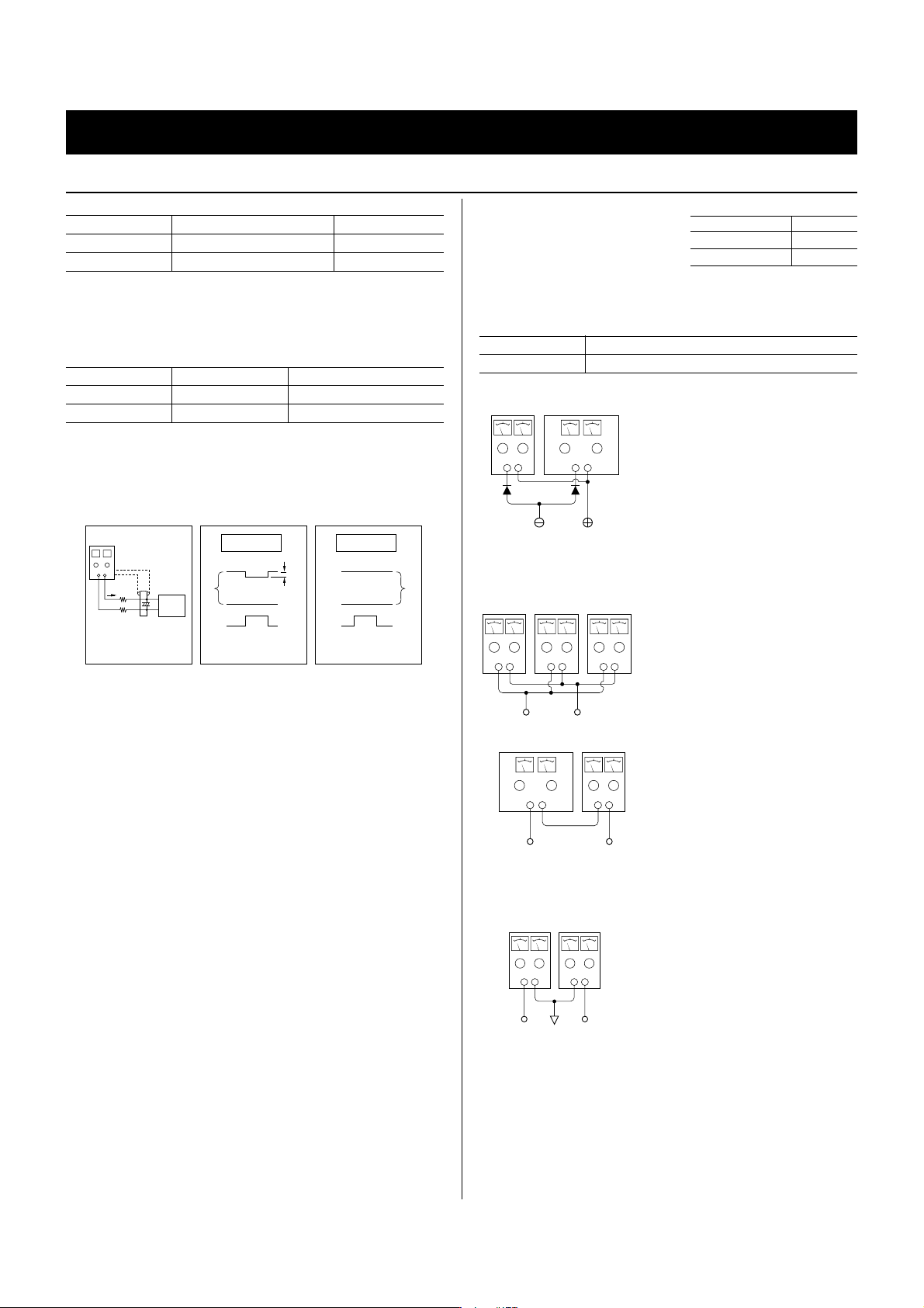
■ Remote control with external voltage
Control objective Control voltage
Output voltage
Output current 0 to 0.5V, 1V
0 to Approx. 10V
*1
*2
Input impedance
Approx. 10kΩ
100kΩ min.
■ Output ON/OFF control
• The output can be turned on and
off with a contact signal from the
outside.
Contact signal Output
ON OFF
OFF ON
*1 Since common is connected to a plus voltage, the control volt-
age must be floating (insulated).
*2
Depends on the model.
■ Remote control with external resistance
Control objective Control resistance Current flowing in resistance
Output voltage 0 to Approx. 10kΩ Approx. 1mA
Output current 0 to 550Ω, 1kΩ Approx. 1mA
• Use a metal film resistor or wirewound resistor with a low temperature coefficient and good ageing stability as the control resistor.
■ Remote sensing
Io
r
+
Load
c
r
Ed=2r ✕ Io:Voltage drop
Before sensing
Eo
Output voltage
Io
Output Current
Ed
Ov
After sensing
Eo
Output voltage
Io
Output Current
• This method compensates the voltage drop using the wiring between the power supply and load and its contact resistance. The
voltage drop becomes a problem as the current increases. However, a drop up to about 1.2V at one side can be prevented by
disconnecting the rear terminal board shorting bar and moving the
voltage sense point to the load side.
(For 0.3V and more, the maximum output voltage must be reduced.)
• Pay careful attention to the polarity and connect an electrolytic
capacity of several hundred µF or more to the sensing terminal
over the shortest distance possible. The is done to prevent the output impedance of the power supply seen from the load from becoming high because if the load line is long, the inductance component cannot be ignored. Especially, for an inverter that interrupts the current at a high frequency and similar loads, connect a
capacitor of several thousand µF or more over the shorest possible
distance.
■ Power tripping
• The input power switch can be tripped with an external contact
signal.
Contact signal Operation
ON Power switch off
■ Parallel operation
• All models in the PAD-L Series can
be set to the same output voltage and
+ー ー+
connected in parallel.
• Connect the PAD-LP Series in parallel through a diode to prevent
burning of the high-speed OVP.
(LP Series)
■ One control parallel operation
(Possible only for parallel connection of the same model.)
Master+ーSlave
Slave
• The current capacity can be increased by connecting the same
model. Output is controlled by one
+ー
master.
+ー
• Perform remote sensing, remote
ー+
control, output on/off, etc. with only
one master.
■ Series operation
• All models in the PAD-L Series can
be connected in series within ground
voltage ±25V. (The maximum cur-
+ーー+
rent when connected in series depends on the model with the lowest
+ー
output current. Always use at current below this value.)
■ One control series operation
Slave Master
• This method increases the output
voltage by connecting power supplies in series. The model at the plus
+ー +ー
side becomes the master. The output of the slave can be controlled
ー+
by operation of only one unit.
• An example of a dual tracking power
supply that can vary the plus and minus sides simultaneously is shown
at the left.
Page3Copyright © 2002 KIKUSUI ELECTRONICS CORP. All rights reserved. http://www.kikusui.co.jp/
Page 4
Load
Since the PAD-L/LP Series meet a wide range of user needs, the use
of various loads is also considered. Depending on the load, the use of
a power supply as is may cause trouble or erroneous operation and
countermeasures must be taken.
PAD-L/PAD-LP series
REGULATED DC POWER SUPPLY (CV·CC)
• When performing remote sensing, always turn the sensing line on
and off simultaneously.
+S
■ High capacity load
L Series
+
output voltage does not drop. With the
• There are no special problems, but the
+
P AD-LP Series, this may cause the high-
LP Series
+
diode in series with the power supply.
speed OVP to burn up. Therfore, insert a
+
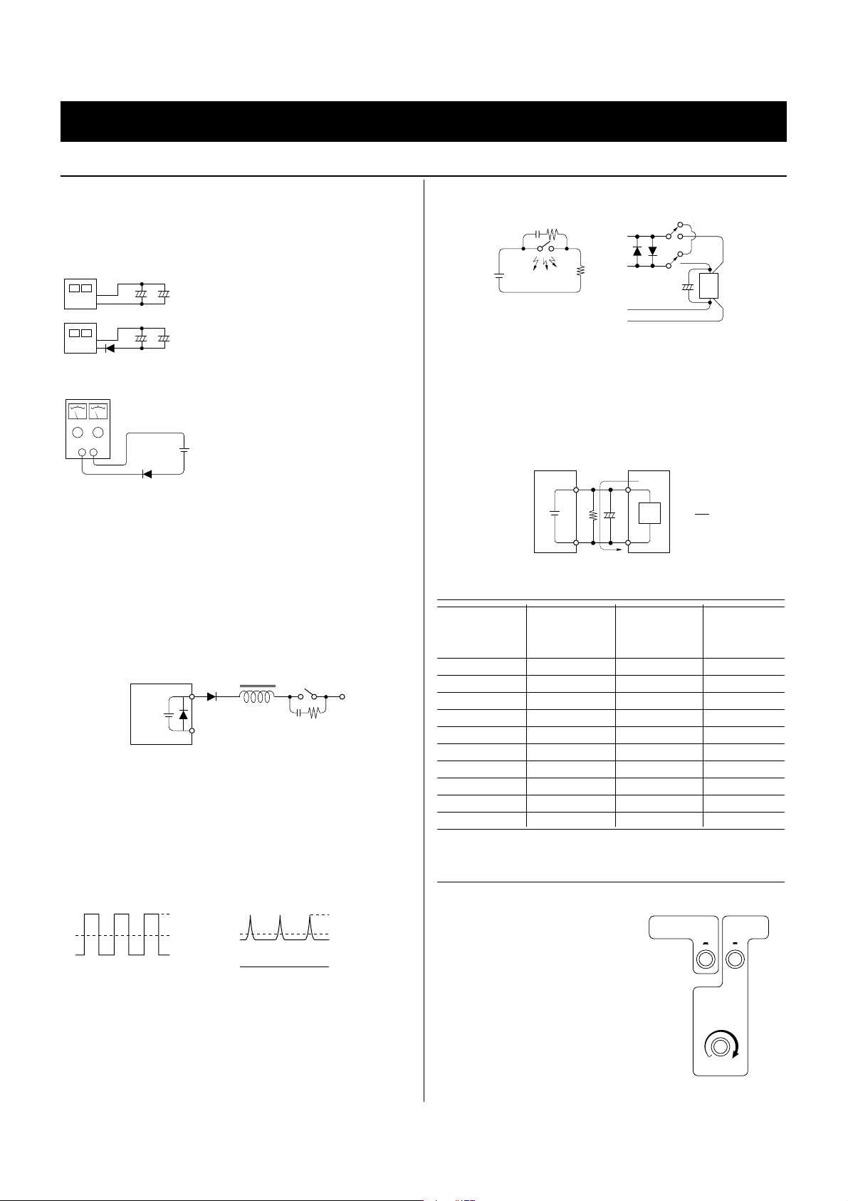
■ Secondary battery (storage battery, Nicd, etc.)
• Use the PAD-LP Series in series with a
diode.
• Since the power supply output electro-
+ー
lytic capacitor charges when the power
supply is connected to the load, sparks
Diode
may fly . The power supply is not abnormal. This fear can be dispelled by making the voltages equal.
■ Inductive load
• The counterelectromotive force generated by turning on and off of
the power supply, or changing the voltage setting is shunted by
protection diode D
1 inserted in parallel with the output so that the
power supply is not damaged.
• When pulse noise generated from an inductive load is impressed
at the same polarity as the power supply, protect the power supply
by inserting diode D
2 in series with the power supply and inserting
a noise prevention CR absorber across the switch.
Diode
2
Power
Supply
D
D
1
CR
■ When the load current has a peak (motor, lamp, etc.)
• When the peak value is within the rated value even through the
load current waveform of a digital circuit or motor drive circuit is
within the rating by meter indication (average value), the current
may momentarily enter the rated current region and the output
voltage will drop and appear to be unstable. The basic countermeasure against this is to increase the output current. However,
when the pulse width is narrow or the peak value is small, install a
large capacitor at the load end.
Peak value
Average value
(meter reading)
When the output is turned ON and off with a mechanical switch
■
Peak value
Average value
0
• When a DC output of 100V or more is opened and closed with a
switch, arc discharge, etc. will cause the switch contacts to noticeably wear and generate noise. This noise may enter the power supply differential amplifier through the load line and cause the output to become unstable. Take noise countermeasures by inserting
a CR absorber near the contacts, the same as for an inductive load.
+
NOISE
RL
ー
ーS
+
RL
■ Load that regenerates a current at the power supply side
• Since the PAD-L Series cannot absorb a reverse current from the
load, and become unstable as the output voltage rises, connect a
dummy load (R) through passes the peak value of the reverse current. When the reverse current is in the form of a spike, install a
large electrolytic capacitor at the load end.
Regenerated current
(reverse current)
I
R
0
+
R
C
Power Supply Load
R=
E
I
R
Wiring
Nominal cross
section area
Recommended
current
as a DC
output line
2(mm2) 10(A) 27(A)
5.5 20 49 3
830612.2
14 50 88 1.2
22 80 115 0.81
38 100 190 0.46
60 217 0.29
80 200 257 0.22
100 298 0.18
150 300 395 0.12
The wiring cross section area and current capacity and resistance value are related.
Semiconductor allowable
temperature 60˚C (Ambient
temperature 30˚C)
Standard DC
resistance 20˚C
Approx. 9[Ω/km]
Features of PAD-LP Series
■ Preset type high-speed OVP (OverVoltage Protector)
• When the output voltage exceeds the
OVP set value, a thyristor short circuits
the output and suppresses the overvoltage and simultaneously trips the power
switch.
• Overvoltages are detected in a fast 200µs.
• The set value can be checked without interrupting the protection operation even while
the power supply is operating.
■ CV (Constant Voltage) and CC (Constant
Current) operation mode display and OVP
operation, or power supply switch tripping,
are sent to the outside by contact output.
CURRENT/VOLT.
LIMIT
PRESET
O.V.P
Page4Copyright © 2002 KIKUSUI ELECTRONICS CORP. All rights reserved. http://www.kikusui.co.jp/
Page 5
PAD-L/PAD-LP series
DISCON
DISCON
DISCON
DISCON
DISCON
DISCON
DISCON
DISCON
DISCON
DISCON
REGULATED DC POWER SUPPLY (CV·CC)
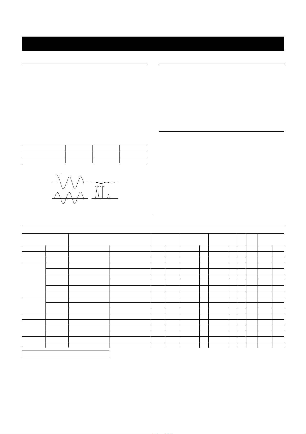
Surge Current
When the power supply is closed, a surge current flows according to
the close timing. Called the “in-rush current”, this surge current causes
magnetic saturation of the core of the transformer and, theoretically,
when the power switch is closed near the 90˚ (π/2) phase angle of the
voltage waveform, surge current does not flow as a transient phenomena. When the switch is closed at the phase angle 0˚ (zero cross)
timing, the maximum current shown in the table below will flow.
Actually, the surge current differs with the hysteresis characteristic
of the core material B-H curve and the direction of the residual flux
with the timing at which the switch was turned off, or the impedance
of the connected AC line.
PAD-L/LP Series typical surge current value (maximum value)
■
(Half value width of current waveform 2 to 5ms)
Type III IV V
AC input voltage 220V 220V 220V
Peak current 700A *200A *400A
*
The Type IV and V are equipped with a built-in surge current prevention circuit as standard.
90°C closing
0˚C closing
Voltage waveform
Peak current
Current waveform
PAD-LP Series Applications
If erroneous operation or trouble should occur, the load can be protected at high-speed and an external alarm can be simultaneously
actuated by contact signal.
• Semiconductor and other loads and electronic circuits with a low
overvoltage resistance
• Automatic systems that use a GPIB programmer (DPO2212A)
• When unmanned reliability tests and life tests are conducted for a
long time
• Systems in which accidents, etc. may impress an overvolt
Computer Control
• The Power Supply has a capable of Computer Control by using
with PIA4800 Series. (For the detailed features of PIA4800 Series,
please refer to Page 5-2)
• The Power Supply has a capable of Computer Control by using
with PIA3200. (For the detailed features of PIA3200, please refer
to Page 5-9)
• The Power Supply has a capable of Computer Control by using
with DPO2212A. (For the detailed features of DPO2212A, please
refer to Page 5-20 )
Specifications
(CV: Constant Voltage mode, CC: Constant Current mode)
Output Model Ripple Load fluctuation
CV CC Standard type High-speed OVP type CV CC CV CC CV CC Type
V A L Series LP Series mVrms mArms
0 to 16 0 to 100 ❍ PAD 16-100L 0.5 100 1325III63200/100 3.3
0 to 50 PAD 35-50L 0.5 10 1325III58200/100 3.3
0 to 60 PAD 35-60L 0.5 10 1325III61200/100 3.8
0 to 35 0 to 100 ❍ PAD 35-100L 0.5 50 1325IV972006.8
0 to 200 ❍ PAD 35-200L 0.5 100 1 30 2 30 V 188 200 13
0 to 200 ❍ PAD 35-200LT 0.5 100 1 30 2 30 V 190 200/3ø 14.5
0 to 300 ❏ PAD 35-300LPT 0.5 200 1 30 2 30 V2220 200/3ø 18
0 to 35 PAD 60-35L 0.5 8 1323III62200/100 3.8
0 to 60 0 to 60 ❍ PAD 60-60L 0.5 20 1325IV992006.8
0 to 120 ❍ PAD 60-120L 0.5 50 1 15 2 15 V 175 200 12
0 to 60 0 to 200 ❏ PAD 60-200LPT 0.5 100 1 30 2 30 V2220 200/3ø 19
0 to 20 PAD 110-20L 1 4 1123III60200/100 3.8
0 to 110 0 to 30 ❍ PAD 110-30L 1 10 1325IV962006
0 to 60 ❍ PAD 110-60L 1 20 1 12 2 10 V 170 200 11
0 to 250
[T] at the end of the Model No. represents 3-phase input.
...... Constant current knobs are coarse and fine adjustment knobs.
❍
...... Constant current knob is 10 turns.
❏
0 to 8 PAD 250-8L *1 5 4 2133III60200/100 3.4
0 to 15 ❍ PAD 250-15L 5 5 2133IV942006.0
Remarks of the input voltage:
100/200 100V-standard / changeable to 200V by user
200/100 200V-standard / changeable to 100V by user
(Other voltage changes are also available upon request.)
Power supply
fluctuation
0.005%+mVmA0.005%+mV
Dimen-
Weight
sions
Approx.
mA kg V kVA
Input
Voltage Power
■ V oltage to ground
±250V DC, However,
*1 type: ±500V DC
Leakage current
• A capacitor is not inserted between the input and the chassis.
There is no danger of circuit breaker erroneous operation and electric shock
even when multiple units are used simultaneously.
Page5Copyright © 2002 KIKUSUI ELECTRONICS CORP. All rights reserved. http://www.kikusui.co.jp/
Page 6
Common specifications
■ Constant voltage temperature coefficient
50p.p.m./˚C (standard value)
■ Transient response time
Time until the output voltage recovers to within
0.05%+10mV of the set value when the output current
changes 5% to 100%.
50µs (Type V: 100µs)
■ Ripple noise
5Hz to 1MHz, ±3dB bandwidth, average value indication,
measured by grounding plus or minus output with an rms
value display AC voltage waveform
■ Indicator
DC voltmeter Type III, IV JIS Class 2.5
Type V, VI JIS Class 1.5
DC ammeter Type III, IV JIS Class 2.5
Type V, VI JIS Class 1.5
■ Ground
Plus or minus terminal can be grounded
■ Insulation resistance
Chassis-input: 500V DC 30MΩ min.
Output-chassis: 500V DC 20MΩ min.
■ Dielectric strength
No abnormalities when 1500VAC applied for 1 minute.
■ Operating temperature range
0 to 40˚C
PAD-L/PAD-LP series
REGULATED DC POWER SUPPLY (CV·CC)
■ Operating humidity range
10 to 90% RH
■ Cooling system
Forced air cooling using a fan
■ Constant voltage operation display color
Green
■ Constant current operation display color
Red
■ Protection devices
● Constant voltage, constant current automatic crossover
● Overvoltage protector (OVP)...L Series
● High-speed overvoltage protector (high-speed OVP)...LP
Series
● Overcurrent protection circuit (110% of output rated cur
rent)
● Overvoltage protection circuit (rectifier smoothing elec-
trolytic capacitor section)
● Overheating protector (OHP)...Semiconductor cooling
heat sink section (100˚C)
● Temperature fuse (subtransformer)
● Temperature switch (Type V main transformer)
● Input/output fuse
● Input surge absorber
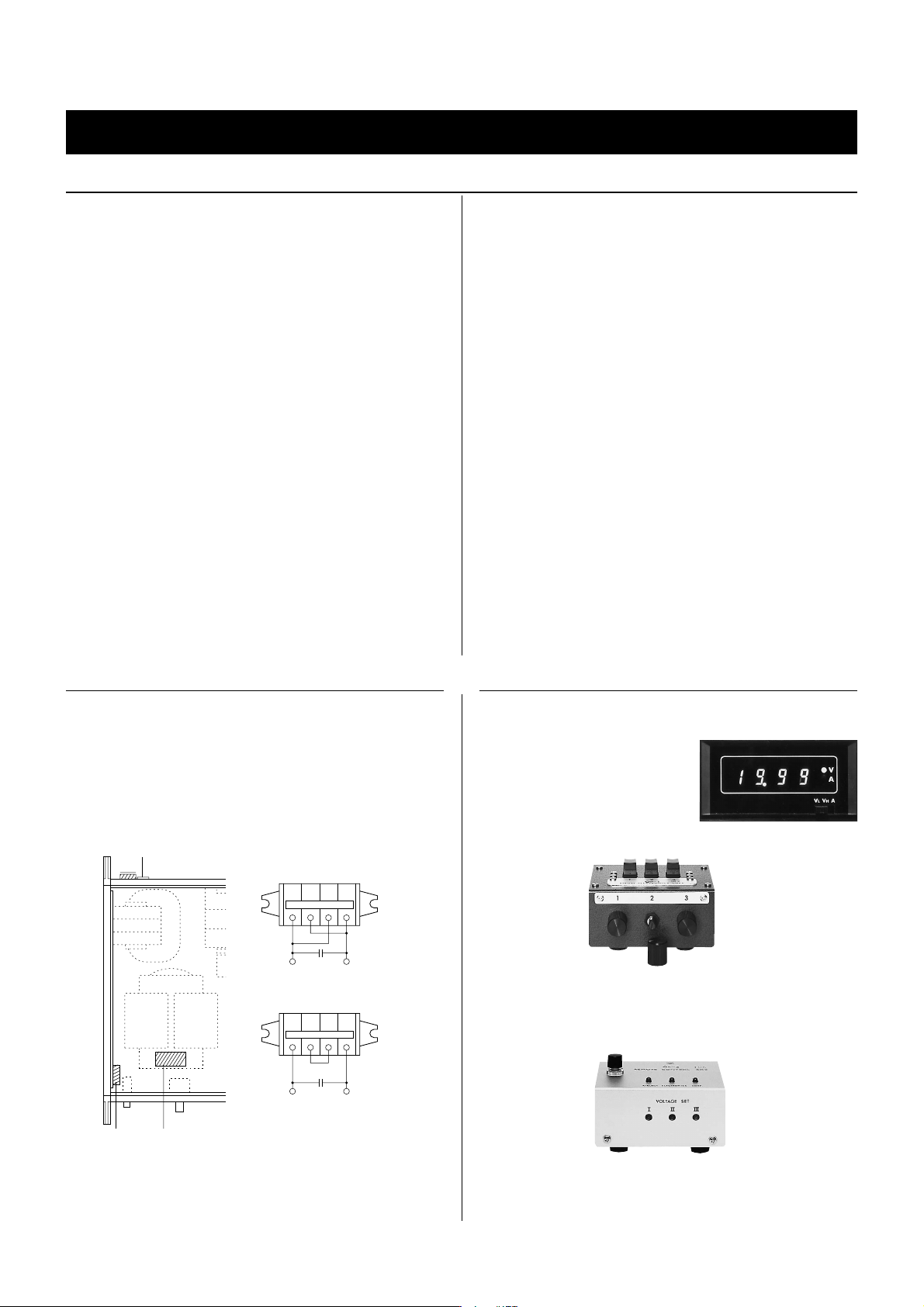
Power supply voltage 100/200V modification
Models with 100/200 entered in the “Input Voltage” column in the
specifications, 100V ±10% or 200V ±10% input voltage power supply can also be used by changing the internal terminal board wiring.
1. The main power transformer terminal board is changed.
2. The input power fuse is changed.
3. The input voltage nameplate is changed.
Input voltage nameplate
100v 0100v 0
AC100V
100v 0100v 0
AC200V
Options
■ DOM -2 digital voltmeter/ammeter
• The DOM-2 is a manually switched 2-range voltmeter and 1-range
ammeter.
• 3 1/2 digits maximum display 1999
LED 7-segment display
• Voltmeter ±(0.1% rdg + 1 digit)
• Ammeter ±(0.5% rdg + 1 digit)
■ OP-1 Output Voltage 3-Point Switching Option
• Three preset voltages can be selected with one touch by pushbutton
switch. (Perfect for adjustment and data acquisition on the assembly line.)
■ OP-2 3-Output Scanning Option
Input fuse Input terminal board
• Three preset voltages can be sequentially switched with a light
touch. (Perfect for adjustment and data acquisition on the assembly line.)
Page6Copyright © 2002 KIKUSUI ELECTRONICS CORP. All rights reserved. http://www.kikusui.co.jp/
 Loading...