

Page 1

Keysight N2750/1/2A
Differential Probes
User’s Guide
Page 2

Notices
© Keysight Technologies, Inc. 2014, 2019
No part of this manual may be reproduced in
any form or by any means (including electronic storage and retrieval or translation into
a foreign language) without prior agreement
and written consent from Keysight Technologies, Inc. as governed by United States and
international copyright laws.
Manual Part Number
N2750–97003
Edition
February 2019
Keysight Technologies, Inc.
1900 Garden of the Gods Road
Colorado Springs, CO 80907 USA
Warranty
The material contained in this document is
provided “as is,” and is subject to being
changed, without notice, in future editions.
Further, to the maximum extent permitted by
applicable law, Keysight disclaims all warranties, either express or implied, with regard
to this manual and any information contained
herein, including but not limited to the
implied warranties of merchantability and fitness for a particular purpose. Keysight shall
not be liable for errors or for incidental or
consequential damages in connection with
the furnishing, use, or performance of this
document or of any information contained
herein. Should Keysight and the user have a
separate written agreement with warranty
terms covering the material in this document
that conflict with these terms, the warranty
terms in the separate agreement shall control.
Technology Licenses
The hardware and/or software described in
this document are furnished under a license
and may be used or copied only in accordance with the terms of such license.
U.S. Government Rights
The Software is "commercial computer
soft-ware," as defined by Federal
Acquisition Regulation ("FAR") 2.101.
Pursuant to FAR 12.212 and 27.405-3
and Department of Defense FAR Supplement ("DFARS") 227.7202, the U.S.
government acquires commercial
computer software under the same
terms by which the software is customarily provided to the public.
Accordingly, Keysight provides the
Software to U.S. government customers under its standard commercial
license, which is embodied in its End
User License Agreement (EULA), a
copy of which can be found at
http://www.keysight.com/find/sweula. The
license set forth in the EULA represents the exclusive authority by
which the U.S. government may use,
modify, distribute, or disclose the Software. The EULA and the license set
forth therein, does not require or permit, among other things, that Keysight:
(1) Furnish technical information
related to commercial computer software or commercial computer software documentation that is not
customarily provided to the public; or
(2) Relinquish to, or otherwise provide,
the government rights in excess of
these rights customarily provided to
the public to use, modify, reproduce,
release, perform, display, or disclose
commercial computer software or
commercial computer software documentation. No additional government
requirements beyond those set forth in
the EULA shall apply, except to the
extent that those terms, rights, or
licenses are explicitly required from all
providers of commercial computer
software pursuant to the FAR and the
DFARS and are set forth specifically in
writing elsewhere in the EULA. Keysight shall be under no obligation to
update, revise or otherwise modify the
Software. With respect to any technical data as defined by FAR 2.101, pursuant to FAR 12.211 and 27.404.2 and
DFARS 227.7102, the U.S. government acquires no greater than Limited
Rights as defined in FAR 27.401 or
DFAR 227.7103-5 (c), as applicable in
any technical data. 52.227-14 (June
1987) or DFAR 252.227-7015 (b)(2)
(November 1995), as applicable in any
technical data.
Safety Notices
CAUTION. A CAUTION notice
denotes a hazard. It calls attention to an
operating procedure, practice, or the
like that, if not correctly performed or
adhered to, could result in damage to
the product or loss of important data.
Do not proceed beyond a CAUTION
notice until the indicated conditions are
fully understood and met.
WARNING. A WARNING notice
denotes a hazard. It calls attention to
an operating procedure, practice, or the
like that, if not correctly performed or
adhered to, could result in personal
injury or death. Do not proceed beyond
a WARNING notice until the indicated
conditions are fully understood and
met.
2 N2750/1/2A User’s Guide
Page 3

Contents
Contents
1Using the Probes
Probe Features / 6
Oscilloscope Compatibility / 7
Bandwidth / 7
Available Accessories / 8
Single-Ended Measurements / 8
Quick-Action Button and
Probe Light / 9
InfiniiMode Compatible / 9
Channel-Identification Rings / 9
Exchangeable Probe Tips / 10
To Attach a Tip / 11
N2776A Browser Tip / 12
Placing the Signal Within the Probe’s Dynamic Range / 15
InfiniiMode / 16
Probe Configuration Dialog Box / 19
Quick-Action Button / 20
Probe Attenuation Ratio / 22
Functional Test / 22
Inspecting the Probe / 23
Cleaning the Probe / 23
Returning the Probe for Service / 24
Contacting Keysight Technologies / 24
Safety Information / 25
Instrument Markings and Safety Symbols / 27
N2750/1/2A User’s Guide 3
Page 4

Contents
2SPICE Models
N2752A probe with the N2776A Browser Tip / 30
N2750A probe with the N2777A Solder-In Tip / 33
Measured Versus Modeled Input Impedance / 36
3 Probe Calibration
Calibrating the Probe / 40
4 Characteristics and Specifications
Dimensions / 46
5Performance Data Plots
With N2776A Browser Tip (2:1 Attenuation) / 48
With N2776A Browser Tip (10:1 Attenuation) / 52
With N2777A Solder-In Tip (2:1 Attenuation) / 53
With N2777A Solder-In Tip (10:1 Attenuation) / 55
With N2778A Socketed Tip (2:1 Attenuation) / 57
With N2778A Socketed Tip (10:1 Attenuation) / 58
6 Performance Verification
Test 1. DC Input Resistance / 62
Procedure / 62
Test 2. Bandwi dth / 63
Calibrate the Test Setup / 63
Measure V
Measure V
Response / 65
in
Response / 69
out
Determine the BW / 71
Performance Test Record / 73
4 N2750/1/2A User’s Guide
Page 5

Keysight N2750/1/2A Differential Probes
User’s Guide
1 Using the Probes
Probe Features 6
Exchangeable Probe Tips 10
Placing the Signal Within the Probe’s Dynamic Range 15
InfiniiMode 16
Quick-Action Button 20
Probe Attenuation Ratio 22
Functional Test 22
Inspecting the Probe 23
Cleaning the Probe 23
Returning the Probe for Service 24
Safety Information 25
The N2750/1/2A differential probes can be used to perform differential, common
mode, and single-ended measurements. The probes have the following
bandwidths:
N2752A: . . . . . . . . . . . . . . . . . . . . . . . . . . . . . . . . . . . . . . . .6 GHz
N2751A: . . . . . . . . . . . . . . . . . . . . . . . . . . . . . . . . . . . . . . 3.5 GHz
N2750A: . . . . . . . . . . . . . . . . . . . . . . . . . . . . . . . . . . . . . . 1.5 GHz
CAUTION These probes are ESD sensitive devices, particularly at the probe tips.
Follow standard ESD precautions when handling. Remove tip
accessories when storing the probe.
CAUTION Before using the probe, refer to “Safety Information” on page 25.
5
Page 6
1 Using the Probes
Probe Features
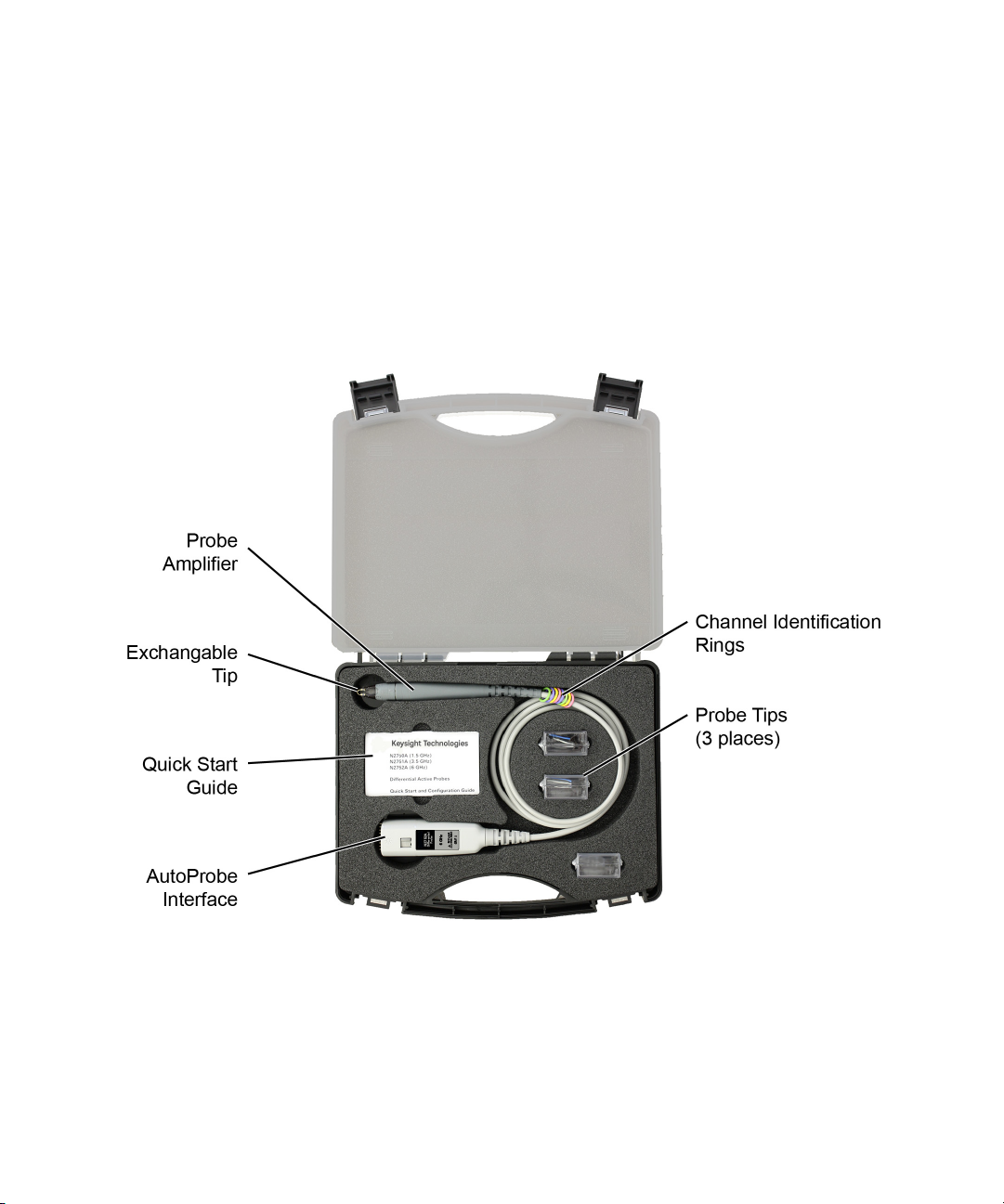
The N2750/1/2A differential probes feature a probe Quick Action button, light,
channel identification rings, and three different exchangeable snap-on probe tips:
browser, solder-in, and socketed. To learn more about the probe tips, refer to
“Exchangeable Probe Tips” on page 10. These probes use the AutoProbe
oscilloscope interface for automatic configuration and power.
Figure 1 Probe with Supplied Accessories and Case
6 N2750/1/2A User’s Guide
Page 7

Oscilloscope Compatibility
The probes are compatible with 9000 Series, 90000 Series, or 90000 Q/X-Series
Infiniium oscilloscopes with software version 3.50 or above. Infiniium 90000
Q/X-Series requires the N5442A adapter. The probes are compatible with
3000X-series InfiniiVision oscilloscopes (one probe maximum connected to
oscilloscope). The probes are also compatible with 4000X-series InfiniiVision
oscilloscopes (up to four probes connected to oscilloscope).
Bandwidth
As shown in the following table, the available probe bandwidth depends on the
probe model, attached probe tip, and type of signal probed. To learn about the
supplied probe tips, refer to “Exchangeable Probe Tips” on page 10.
Table 1 Available Probe Bandwidth
Using the Probes 1
Browser Probe
Signal Type
N2752A 6 GHz at 2:1 / 10:1
Differential 6 GHz
Single-Ended 6 GHz
Common-Mode N/A 1 GHz 1.4 GHz
N2751A 3.5 GHz at 2:1 / 10:1
Differential 3.5 GHz 3 GHz 2.5 GHz
Single-Ended 3.5 GHz 1.2 GHz 2 GHz
Common-Mode N/A 1 GHz 1.4 GHz
N2750A 1.5 GHz at 2:1 / 10:1
Differential 1.5 GHz 1.5 GHz 1.5 GHz
Single-Ended 1.5 GHz 1.2 GHz 1.5 GHz
Common-Mode N/A 1 GHz 1.4 GHz
Tip
(7 GHz typical)
(7 GHz typical)
Socketed Probe
Tip
3 GHz 2.5 GHz
1.2 GHz 2 GHz
Solder-In Probe
Tip
N2750/1/2A User’s Guide 7
Page 8

1 Using the Probes
Available Accessories
The following table shows the accessories that are available for use with the
probes.
Table 2 Available Accessories
Model
Number
N5442A Precision BNC adapter for use with 90000 Q/X-Series oscilloscopes
N2787A 3D probe positioner
Accessory
E2655B/C or
N5443A
Performance verification and deskew fixture. The PV fixture
is used in Chapter 3, “Probe Calibration”and Chapter 6,
“Performance Verification”.
Single-Ended Measurements
You can use the differential probes to make single-ended measurements by
touching one probe tip to the ground on the device being tested. In fact, using
these differential probes in any situation where a single-ended probe would
traditionally be used results in higher Common Mode Rejection Ratio (CMRR),
increased signal fidelity (due to very low impedance grounding and higher input
impedance), and decreased probe response variations (better repeatability).
8 N2750/1/2A User’s Guide
Page 9

Quick-Action Button and Probe Light
Press the quick-action button to turn the probe light on and off. Pressing and
holding the button will increase and decrease the light’s intensity. Using the
oscilloscope’s Probe Configuration dialog box, you can re-assign the button’s
function. Refer to “Quick-Action Button” on page 20.
Figure 2 Location of Button and Light
InfiniiMode Compatible
The probes, when fitted with the socketed or solder-in tip, are InfiniiMode
compatible. InfiniiMode allows you to switch between differential, single-ended,
and common mode measurements without needing to change or reconnect the
probe or probe leads. To learn about this feature, refer to “InfiniiMode” on
page 16.
Using the Probes 1
Channel-Identification Rings
When multiple probes are connected to the oscilloscope, the channel
identification rings allow you to quickly determine which channel input is
associated with each probe. On the probe, place one colored ring near the probe’s
channel connector and place an identical color ring near the probe head.
CAUTION Handle the probe cable carefully to avoid damaging it through excessive
bending or pulling. Avoid any mechanical shocks to the probe in order to
guarantee accurate performance and protection.
N2750/1/2A User’s Guide 9
Page 10

1 Using the Probes
Exchangeable Probe Tips
The probe comes with three unique tips for different probing situations. They are
the browser, solder-in, and socketed tips as shown in Table 3 and described later
in this section. For information on using the solder-in and socketed tips with
InfiniiMode, refer to “InfiniiMode” on page 16.
The tip’s symmetrical design allows you to orient the tip so that either lead (for
example, the blue lead on N2777A and N2778A tips) can be associated with the
probe’s A or B sides. Refer to “InfiniiMode” on page 16 for the significance of the A
and B leads in differential measurements.
Table 3 Supplied Probe Tips
Tip Quantity Replacement Tip Kit
Differential Browser Tip (adjustable span)
described on page 12.
InfiniiMode Solder-In Tip described on page 13. 2 N2777A
InfiniiMode Socketed Tip described on page 14. 2 N2778A
2 N2776A
(includes three browser tips)
(includes three solder-in tips)
(includes three socketed tips)
10 N2750/1/2A User’s Guide
Page 11

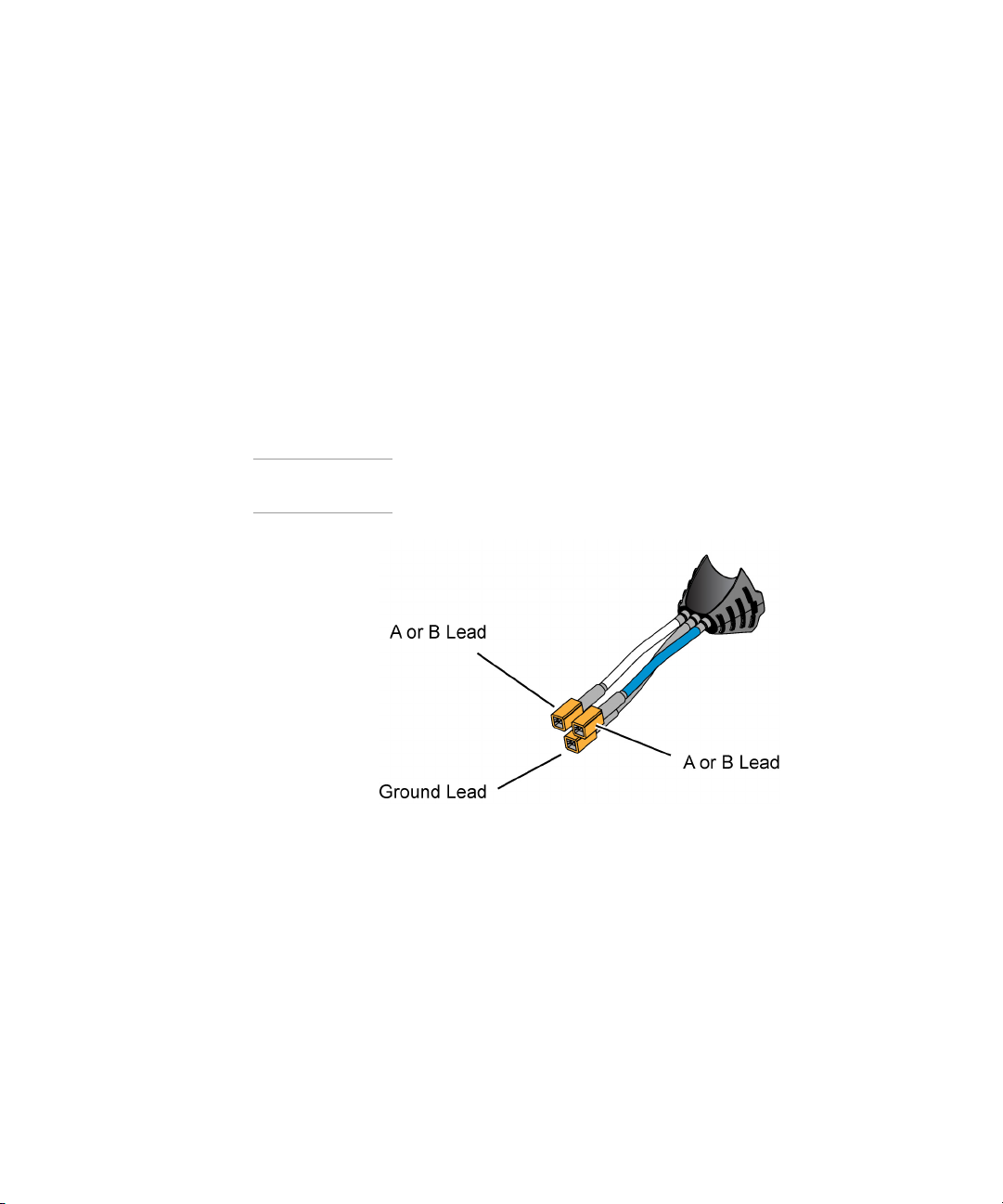
To Remove a Tip
Hold the probe in one hand while holding the body of the tip in the other hand.
Gently pull the probe tip straight off the probe.
CAUTION Do not remove the tip by pulling on the tip leads.
Figure 3 Do not pull on the tip leads
Using the Probes 1
To Attach a Tip
1 Orient the new tip as shown in the following figure. For solder-in and socketed
tips, you can orient the tip such that the blue lead is labeled lead A or B.
2 Gently press the tip onto the probe. Never apply excessive force when attaching
the tip.
Figure 4 Aligning the Tip to the Probe
N2750/1/2A User’s Guide 11
Page 12

1 Using the Probes
N2776A Browser Tip
The N2776A browser tip allows you to quickly probe the different points in your
device. The tip includes integrated damping resistors. To adjust the tip spacing,
turn the handles that are located on the tip ends as shown in Figure 5. Spacing
can range between 0.5 mm and 7.5 mm.
The probes have the following bandwidths when using these tips:
N2752A Probe Amplifier: . . . . . . . . . . . . . . . . . . . . . . . . . . .6 GHz
N2751A Probe Amplifier: . . . . . . . . . . . . . . . . . . . . . . . . . 3.5 GHz
N2750A Probe Amplifier: . . . . . . . . . . . . . . . . . . . . . . . . . 1.5 GHz
As the N2776A browser tip can only be used in differential mode, it is not
compatible with InfiniiMode.
Figure 5 Browser Tip with Spacing Adjustment
12 N2750/1/2A User’s Guide
Page 13

N2777A Solder-In Tip
The N2777A solder-in tip is intended to be soldered directly to your test device.
The tip includes integrated damping resistors. For best performance, use this tip in
differential mode with inputs A and B connected to test nodes.
The probes have the following bandwidths when using this tip:
N2752A Probe Amplifier: . . . . . . . . . . . . . . . . . . . . . . . . . 2.5 GHz
N2751A Probe Amplifier: . . . . . . . . . . . . . . . . . . . . . . . . . 2.5 GHz
N2750A Probe Amplifier: . . . . . . . . . . . . . . . . . . . . . . . . . 1.5 GHz
When installing the tip on the probe, the tip’s symmetrical design allows you to
orient the tip so that the blue lead can be located on the probe’s A or B side.
NOTE The color and position of the leads is not important except to allow you to
Using the Probes 1
easily distinguish between the A and B leads.
Figure 6 Solder-In Tip
N2750/1/2A User’s Guide 13
Page 14
1 Using the Probes
N2778A Socketed Tip
Use the N2778A socketed tip for connecting the probe directly to 0.25-inch
header pins. For best performance, use this tip in differential mode with inputs A
and B connected to test nodes. The socketed leads include a damping resistor.
The probes have the following bandwidths when using this tip:
N2752A Probe Amplifier: . . . . . . . . . . . . . . . . . . . . . . . . . . .3 GHz
N2751A Probe Amplifier: . . . . . . . . . . . . . . . . . . . . . . . . . . .3 GHz
N2750A Probe Amplifier: . . . . . . . . . . . . . . . . . . . . . . . . . 1.5 GHz
When installing the tip on the probe, the tip’s symmetrical design allows you to
orient the tip so that the blue lead can be located on the probe’s A or B side.
NOTE The color and position of the leads is not important except to allow you to
easily distinguish between the A and B leads.
Figure 7 Socketed Tip
14 N2750/1/2A User’s Guide
Page 15

Placing the Signal Within the Probe’s Dynamic Range
When making single-ended or common mode measurements, you can apply
vertical offset to place the signal within the probe’s dynamic range. Vertical offset
centers a signal at 0V on the oscilloscope’s display by compensating for the
signal’s DC component. The red signal in Figure 8 has a +4V DC component. The
green signal show the result of applying –4V vertical offset.
Figure 8 Vertical Offset Applied to an Input Signal
Using the Probes 1
NOTE The above figure uses an example offset of –4V. The actual available range is
dependent on the oscilloscope. Refer to the oscilloscope’s vertical offset
specification that is located in the help system.
N2750/1/2A User’s Guide 15
Page 16

1 Using the Probes
InfiniiMode
The probes, when fitted with a socketed or solder-in tip, are InfiniiMode
compatible. InfiniiMode allows you to switch between differential, single-ended,
and common mode measurements without needing to change or reconnect the
probe or probe leads. The following table shows, depending on the probe tip and
InfiniiMode setting, which signal types can be measured.
Table 4 Supported InfiniiMode Measurements by Probe Tip
Signal Being Measured
InfiniiMode
Setting
Differential Browser (full BW)
Single-Ended Browser (not supported) Browser (not supported)
Single-Ended Differential
a
Solder-In (lower BW) Solder-In (lower BW)
Socketed (lower BW) Socketed (lower BW)
Solder-In Solder-In
Browser (full BW)
Socketed Socketed
Common-Mode Browser (not supported) Browser (not supported)
Solder-In Solder-In
Socketed Socketed
a Full bandwidth obtained by touching one tip to ground.
NOTE Because the N2776A browser tip has two leads instead of three, it is not
InfiniiMode compatible. However, you can still use the browser tip to
measure single-ended signals by selecting differential mode and touching
one tip to ground.
16 N2750/1/2A User’s Guide
Page 17
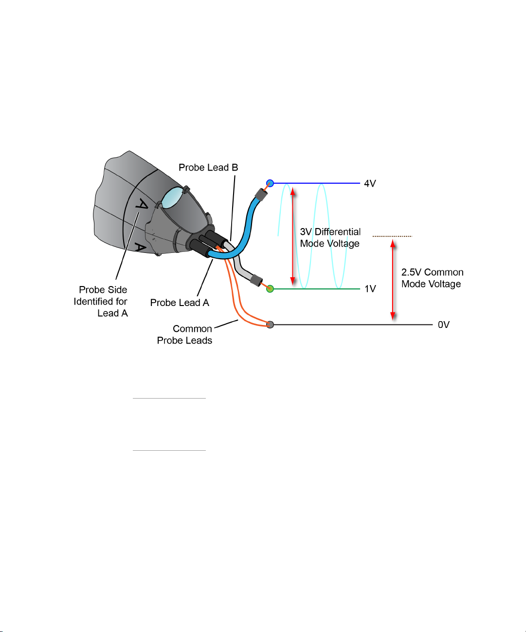
Making InfiniiMode Connections
When probing a differential or common mode signal, connect the probe tips as
shown in the example circuit of Figure 9. Notice that the sides of the probe are
marked A and B to identify the two signal leads.
Using the Probes 1
Figure 9 Example InfiniiMode Probe Circuit Connections
NOTE The lead’s color allows you to easily distinguish between the A and B leads.
Figure 9 shows the blue lead oriented so that it is lead A. The tip could
easily be removed and rotated 180° so that the blue lead becomes the B
lead.
N2750/1/2A User’s Guide 17
Page 18

1 Using the Probes
AB–4V1V–3V==
AB+
2
-------------
4V 1V+
2
---------------------
2.5V==
A gnd–4V0V–4V==
B gnd–1V0V–1V==
The following measurements can be made without reconnecting the probe tips. In
the equations, the A and B variables represent the signal from the A and B probe
leads.
Figure 10 Lead Identification on Probe Body
Differential
Common Mode
Single-Ended A
Single-Ended B
18 N2750/1/2A User’s Guide
Page 19

Probe Configuration Dialog Box
When the probe is connected to an Infiniium oscilloscope (9000 Series, 90000
Series, or 90000 Q/X-Series), the Probe Configuration dialog box automatically
opens as shown in Figure 11. The oscilloscope automatically detects the signal
type, which is indicated in the dialog box.
In the dialog box’s InfiniiMode field, select the measurement mode: Differential,
Single-Ended A, Single-Ended B, or Common Mode. The default setting is Differential.
Using the Probes 1
Figure 11 Probe Configuration Dialog Box
NOTE You can also open this dialog box by clicking Utilities > Probe
Configuration.
NOTE The probes have a 2 GHz bandwidth when used with InfiniiMode.
N2750/1/2A User’s Guide 19
Page 20

1 Using the Probes
Quick-Action Button
By default, the probe’s quick-action button turns the probe light on and off.
However, you can reassign this button to another function by using the
oscilloscope’s Probe Configuration dialog box.
NOTE Requires a 9000 Series, 90000 Series, or 90000 Q/X-Series Infiniium
To reassign the probe button, click Utilities > Probe Configuration. In the Probe
Configuration dialog box, click the tab for the N2750A, N2751A, or N2752A probe
and then select the desired action in the Quick Action field.
oscilloscope with software version 3.50 or above.
Figure 12 Probe Configuration Dialog Box
20 N2750/1/2A User’s Guide
Page 21

Quick Action Selections
You can select one of the following probe button Quick Actions.
Toggl e Hea dlig ht
Turns the probe light on and off. This is the default button configuration.
Adjust Headlight Intensity
Hold the button down, and the light’s intensity increases and decreases.
Run/Stop
Toggles between continuous data acquisition and stopping data acquisition.
Single
Initiates a single data acquisition.
Clear Display
Using the Probes 1
Clears the current data from the display.
Autoscale
Performs an autoscale of the displayed waveform.
Multipurpose
Assigns the currently configured Multipurpose function to the probe button. To
select from among the following Multipurpose functions, click Utilities > Customize
Multipurpose:
QuickMeas
?
QuickPrint
?
QuickScreen
?
QuickSetup
?
QuickWaveform
?
QuickEmail
?
QuickExecute
?
QuickControl
?
N2750/1/2A User’s Guide 21
Page 22

1 Using the Probes
Refer to the oscilloscope’s online help for information on Multipurpose functions.
No Action
Disables the probe button.
Probe Attenuation Ratio
The probe’s attenuation ratio can be set to 2:1 or 10:1. When you attach the probe
to the Infiniium oscilloscope, the AutoProbe interface automatically sets the probe
attenuation to the value necessary to make the dynamic range of the probe
greater or equal to the level required to measure the current input signal.
Functional Test
Use the following generic measurement procedure to ensure that your probe is
functioning properly.
1 Connect the probe to an oscilloscope channel input and ensure the input
impedance of the oscilloscope matches the output impedance of the probe
(50W).
2 On the oscilloscope, click Utilities > Calibration Output to assign probe
compensation (Probe Comp) to the AUX Output connector.
3 Connect the probe tip to the oscilloscope’s front-panel AUX Output connector.
4 Press the oscilloscope’s [Auto Scale] button.
5 If the probe is functioning properly, a square wave should now be displayed on
the oscilloscope.
22 N2750/1/2A User’s Guide
Page 23

Inspecting the Probe
• Inspect the shipping container for damage.
Keep the damaged shipping container or cushioning material until the contents
of the shipment have been checked for completeness and the probe has been
checked mechanically and electrically.
• Check the accessories.
• If the contents are incomplete or damaged, notify your Keysight Technologies
Sales Office.
• Inspect the probe.
If there is mechanical damage or defect, or if the probe does not operate properly
or pass calibration tests, notify your Keysight Technologies Sales Office.
If the shipping container is damaged, or the cushioning materials show signs of
stress, notify the carrier as well as the sales office. Keep the shipping materials for
the carrier’s inspection. The sales office will arrange for repair or replacement at
Keysight Technologies’ option without waiting for claim settlement.
Using the Probes 1
Cleaning the Probe
Disconnect the probe from the oscilloscope and clean the probe with a soft cloth
dampened with a mild soap and water solution. Make sure the probe is completely
dry before reconnecting it to an oscilloscope.
N2750/1/2A User’s Guide 23
Page 24

1 Using the Probes
Returning the Probe for Service
If the probe is found to be defective we recommend sending it to an authorized
service center for all repair and calibration needs. Perform the following steps
before shipping the probe back to Keysight Technologies for service.
1 Contact your nearest Keysight sales office for information on obtaining an RMA
number and return address.
2 Write the following information on a tag and attach it to the malfunctioning
equipment.
• Name and address of owner
• Product model number (for example, N2751A)
• Product Serial Number (for example, MYXXXXXXXX)
• Description of failure or service required
NOTE Include probing and browsing tips if you feel the probe is not meeting
performance specifications or a yearly calibration is requested.
3 Protect the probe by wrapping in plastic or heavy paper.
4 Pack the probe in the original carrying case or if not available use bubble wrap
or packing peanuts.
5 Place securely in sealed shipping container and mark container as "FRAGILE".
NOTE If any correspondence is required, refer to the product by serial number and
model number.
Contacting Keysight Technologies
For technical assistance, contact your local Keysight Call Center.
• In the Americas, call 1 (800) 829-4444
• In other regions, visit http://www.keysight.com/find/assist
Before returning an instrument for service, you must first call the Call Center at 1
(800) 829-4444.
24 N2750/1/2A User’s Guide
Page 25

Safety Information
To avoid personal injury and to prevent fire or damage to this product or products
connected to it, review and comply with the following safety precautions. Be aware
that if you use this probe assembly in a manner not specified, the protection this
product provides may be impaired.
WARNING Handle Probe Tips and Accessories Carefully.
WARNING Use Only Grounded Instruments.
WARNING Connect and Disconnect Properly.
Using the Probes 1
Some of the probe tips and accessories are very sharp (the browser tips, for
example). You should handle these with care to avoid personal injury.
Do not connect the probe’s ground lead to a potential other than earth
ground. Always make sure the probe and the oscilloscope are grounded
properly.
Connect the probe to the oscilloscope and connect the ground lead to earth
ground before connecting the probe to the circuit under test. Disconnect
the probe input and the probe ground lead from the circuit under test
before disconnecting the probe from the oscilloscope.
WARNING Observe Probe Ratings.
Do not apply any electrical potential to the probe input which exceeds the
maximum rating of the probe. Make sure to comply with the voltage versus
frequency derating curve found in this manual.
These probes are for use only on circuits that are NOT directly connected to
mains. These are NOT intended for measurements on CAT II, CAT III, or CAT
IV circuits.
WARNING Keep Away From Live Circuits.
Avoid open circuitry. Do not touch connections or components when power
is present.
WARNING Indoor Use Only.
Do not operate in wet/damp environments. Keep product surfaces dry and
clean.
N2750/1/2A User’s Guide 25
Page 26

1 Using the Probes
CAUTION The probe cable is a sensitive part of the probe and, therefore, you should
be careful not to damage it through excessive bending or pulling. Avoid
any mechanical shocks to this product in order to guarantee accurate
performance and protection.
CAUTION Periodically inspect the probe and probe wires to check for any damage.
Do Not Operate With Visible or Suspected Failures. If you suspect there
is damage, have it inspected by a Keysight authorized service personnel.
26 N2750/1/2A User’s Guide
Page 27
Instrument Markings and Safety Symbols
Symbol Description
STANDBY and AC symbols. The STANDBY marks the position of the instrument power
line switch. The AC symbol is used to indicate the required nature of the line
module input power.
The CE mark is a registered trademark of the European Community. ISM GRP 1-A
denotes the instrument is an Industrial Scientific and Medical Group 1 Class A product. ICES/NMB-001 indicates product compliance with the Canadian Interference-Causing Equipment Standard.
The CSA mark is a registered trademark of the Canadian Standards Association.
The C-Tick mark is a registered trademark of the Australian Spectrum Management
Agency.
This product complies with the WEEE Directive (2002/96/EC) marking requirements.
The affixed label indicates that you must not discard this electrical/electronic product in domestic household waste. Product Category: With reference to the equipment
types in the WEEE Directive Annex I, this product is classed as a “Monitoring and Control instrumentation” product. Do not dispose in domestic household. To return
unwanted products, contact your local Keysight office, or refer to www.keysight.com
for more information.
This symbol indicates the Environmental Protection Use Period (EPUP) for the product’s toxic substances for the China RoHS requirements.
Using the Probes 1
Recycle marking.
N2750/1/2A User’s Guide 27
Page 28

1 Using the Probes
28 N2750/1/2A User’s Guide
Page 29

Keysight N2750/1/2A Differential Probes
User’s Guide
2 SPICE Models
N2752A probe with the N2776A Browser Tip 30
N2750A probe with the N2777A Solder-In Tip 33
This chapter presents input impedance SPICE models for the combinations of
N2752A probe with N2776A Browser tip and N2750A probe with N2777A solder-in
tip. SPICE sub-circuit file listings are provided so that you can copy and paste the
data into your SPICE simulations.
29
Page 30

2 SPICE Models
N2752A probe with the N2776A Browser Tip
The following SPICE RLC circuit models the input impedance of the N2752A and
N2776A combination. See Figure 14 on page 32 to view the matching between
the measured and modeled input impedance.
Figure 13 SPICE Model
30 N2750/1/2A User’s Guide
Page 31

SPICE Data
Copy and paste the following lines of data into your SPICE simulations.
.subckt N2750_Browser 1 2
C7 15 5 153f
L9 5 4 1n
R16 4 3 231
C1 15 8 60f
C2 15 10 835f
L1 8 7 1.2n
L2 10 9 6.3n
R1 7 3 7.7
R2 9 3 25
C4 3 20 71f
L4 20 21 6.7n
R4 21 12 1
C3 3 22 129f
L3 22 23 27.6n
R3 23 12 149
C6 12 16 60f
L6 16 17 1.2n
R6 17 15 7.7
C8 12 13 153f
L10 13 14 1n
R17 14 15 231
C5 12 18 835f
L5 18 19 6.3n
R5 19 15 25
R7 3 1 78
R8 12 2 78
R11 11 15 228
L8 11 0 2n
L7 15 0 7.6µ
R9 15 3 100k
R10 12 15 100k
.end
SPICE Models 2
N2750/1/2A User’s Guide 31
Page 32

2 SPICE Models
Measured Versus Modeled Input Impedance
The following plot shows how well the modeled impedance tracks the measured
impedance.
Figure 14 Input Impedance, Measured and Modeled (Differential)
32 N2750/1/2A User’s Guide
Page 33

N2750A probe with the N2777A Solder-In Tip
The following SPICE RLC circuit models the input impedance of the N2750A and
N2777A combination. Observe the following items when positioning the tip wires:
• It is assumed that the tip wires are approximately parallel and connected to the
target at approximately 100 mils spacing.
• As shown in Figure 15, the tip wires are assumed to be kept roughly parallel
from the N2750A probe to the solder-in point. Dramatically spreading the tip
wires to cover a large span, significantly alters the input model and a new
model would be needed.
• Pin 1 is the + input, pin 2 is the – input and pin 3 is the ground connection.
• The impedance is not a strong function of the orientation of the tip wires (for
example, vertical or flat) as long as, when flat, the tip wires are not positioned
down on the ground plane surface.
SPICE Models 2
Figure 15 Nominal Connections
NOTE Do not infer any transfer function accuracy from this model.
N2750/1/2A User’s Guide 33
Page 34

2 SPICE Models
Figure 16 SPICE Model
34 N2750/1/2A User’s Guide
Page 35

SPICE Data
Copy and paste the following lines of data into your SPICE simulation deck.
.subckt N2777A_N2750A_InputZ 1 2 3
C25 1 2 53.7f
R1 1 4 129.3
R2 2 5 129.3
C1 4 3 82.1f
c4 3 5 82.1f
c6 4 5 1.965f
l1 4 6 5.14n
l3 5 7 5.14n
l2 3 8 5.82n
c5 6 7 3.929f
c8 6 8 164.2f
c9 8 7 164.2f
l4 6 9 5.14n
l5 7 10 5.14n
l6 8 11 5.82n
c10 9 10 3.929f
c14 9 11 164.2f
c15 11 10 164.2f
l7 9 12 5.14n
l8 10 13 5.14n
l9 11 14 5.82n
c16 12 13 1.965f
c18 12 14 82.1f
c17 14 13 82.1f
c19 12 14 655f
c20 13 14 655f
c21 12 13 40f
rprc1 15 12 100k
cprc1 15 12 300f
rprc2 16 13 100k
cprc2 16 13 300f
r3 14 15 50
r4 14 16 50
l10 0 14 30u
l11 17 14 2n
r5 0 17 250
k6 l1 l2 .3794
k5 l1 l3 .0954
k4 l2 l3 .3794
SPICE Models 2
N2750/1/2A User’s Guide 35
Page 36

2 SPICE Models
Measured Versus Modeled Input Impedance
k9 l4 l6 .3794
k8 l4 l5 .0954
k7 l6 l5 .3794
k12 l7 l9 .3794
k11 l7 l8 .0954
k10 l9 l8 .3794
.ends
The following plots show how well the modeled impedance tracks the measured
impedance. The model agrees very well out to approximately 5 GHz. Above 5 GHz,
the single-ended and differential models are fairly accurate but the common mode
model degrades because of outside mode uncertainties.
Figure 17 Single-Ended Input Impedance (Measured, Modeled)
36 N2750/1/2A User’s Guide
Page 37

Figure 18 Differential Input Impedance (Measured, Modeled)
SPICE Models 2
Figure 19 Common Mode Input Impedance (Measured, Modeled)
N2750/1/2A User’s Guide 37
Page 38

2 SPICE Models
38 N2750/1/2A User’s Guide
Page 39

Keysight N2750/1/2A Differential Probes
User’s Guide
3 Probe Calibration
Always calibrate the probe before making any critical measurements. A probe
calibration removes attenuation errors, offset errors, and timing delays that are
introduced by the probe. Additional information on the probe calibration
procedure is located in the oscilloscope’s online help.
Probe calibrations vary slightly between 9000 Series, 90000 Series, and 90000
Q/X-Series oscilloscopes. For 9000 Series oscilloscopes, the following calibrations
are used:
•Skew Calibration
• Attenuation/Offset Calibration
For 90000 Series oscilloscopes, the following calibrations are used:
• DC Attenuation/Offset Calibration
•Skew Calibration
• AC Response Calibration
NOTE When performing the attenuation and offset calibrations, the probe is not
connected to any signal sources. During the skew calibration, the probe is
connected to the oscilloscope’s calibration output signal via a PV fixture.
When performing the skew calibration and AC Response calibration, the E2655B
or N5443A Performance Verification (PV) and deskew fixture is used. The PV
fixture is included with the Deskew Kit which is shipped with Infiniium
oscilloscopes. The fixture is also used in the performance verification procedure
that is documented in Chapter 6, “Performance Verification”.
39
Page 40

3 Probe Calibration
Calibrating the Probe
An optional N2787A 3D Probe Positioner or equivalent can be used
to hold the probe during the calibration.
CAUTION Always wear an ESD wrist strap when working with active probes. Not
doing so can result in the probe becoming permanently damaged.
1 Turn on the oscilloscope. Allow the oscilloscope and probe to warm up for 20
minutes before performing the probe calibrations.
2 If the oscilloscope needs calibration, perform a user calibration before the
probe calibration. On the oscilloscope, click Utilities > Calibration.
3 On the oscilloscope, click Setup > Probes.
4 In the Probe Calibration dialog box, select the tab representing the channel that
has the probe attached.
5 In the dialog box, select the probe head and the type of calibration. Click Start
and follow the instructions shown on the oscilloscope.
6 When performing the skew calibration, you will be instructed to use the PV
fixture. Observe these points:
• Connect the PV fixture’s input to the oscilloscope’s calibration output. Connect
a 50 ohm terminator to the PV’s output as shown in Figure 20.
Figure 20 E2655B PV Fixture with 50 Ohm Termination
40 N2750/1/2A User’s Guide
Page 41

Probe Calibration 3
• Clamp the probe leads to the PV fixture’s signal or ground. Position the probe
tips on the PV fixture as shown in Figure 21. When using the solder-in tip, use
the fixture’s spring-loaded clamps to hold the leads.
Figure 21 Example of Proper Lead Placement on an E2655B PV Fixture (Browser Tip
Shown)
• On 90000 Q/X-Series oscilloscopes, use an N5442A adapter when instructed to
connect the probe to one of the oscilloscope’s channel inputs.
CAUTION To avoid damaging the oscilloscope’s Cal Out connector, do not apply
force to the PV fixture. Light probe contact is all that is needed for the
calibration.
CAUTION NEVER solder a probe tip to the thick-film gold. The gold will
immediately dissolve into the solder and disappear.
NOTE If you are using the browser tip, it is recommended that you use the N2787A
3D Probe Positioner to hold the probe in place.
NOTE You can check that the probe leads are correctly connected by pressing the
front panel autoscale button. A stable step should be shown on the screen.
Pressing autoscale will close the Probe Calibration dialog box.
N2750/1/2A User’s Guide 41
Page 42

3 Probe Calibration
42 N2750/1/2A User’s Guide
Page 43

Keysight N2750/1/2A Differential Probes
User’s Guide
4 Characteristics and
Specifications
This chapter provides the characteristics and specifications for the N2750/1/2A
differential active probes. The probe and oscilloscope should be warmed up for at
least 20 minutes before any testing and the environmental conditions should not
exceed the probe’s specified limits.
43
Page 44

4 Characteristics and Specifications
Table 5 Electrical Characteristics and Specifications (Sheet 1 of 2)
Model Number N2750A N2751A N2752A
Probe Bandwidth (–3 dB)
a
Rise time, probe only (10 – 90%) 233 ps 100 ps 58.3 ps
System Bandwidth
(with Keysight oscilloscope)
Input Resistance (at DC)
a
Input Capacitance 700 fF (with browser)
Attenuation Ratio (at DC) 2:1 / 10:1
Input Dynamic Range ± 1Vdc, 2Vpp (@ 2:1) mains isolated
Input Common-Mode Range ±15V (dc to 100 Hz)
Offset Range ±15V
Offset Accuracy
c
Maximum Non-Destructive Input
Voltage
Common Mode Rejection Ratio 60 dB at 1 MHz
Differential Mode Rejection Ratio 50 dB at 1 MHz
Channel Isolation, at single-ended
mode
Offset Gain Accuracy < 3% before calibration
Noise Referred to Input 2.5 mV
1.5 GHz 3.5 GHz 6 GHz (warranted),
1 GHz
(with Keysight’s 1 GHz
Infiniium oscilloscope)
2.5 GHz
(with Keysight’s 2.5 GHz
Infiniium oscilloscope)
(with Keysight’s 4/6 GHz
Infiniium oscilloscope)
200 kΩ ± 2% (differential mode)
100 kΩ ± 2% (single-ended mode)
50 kΩ ± 2% (common mode)
± 5Vdc, 10Vpp (@ 10:1) mains isolated
±2.5V (>100 Hz)
b
< 3% (characteristic)
±30V (DC + peak AC) mains isolated
50 dB at 30 MHz
30 dB at 1 GHz
50 dB at 30 MHz
40 dB at 1 GHz
60 dB at 1 MHz
45 dB at 30 MHz
20 dB at 1 GHz
< 1% after calibration
(at 2:1)
rms
(at 10:1)
7 mV
rms
7 GHz (typical)
4/6 GHz
44 N2750/1/2A User’s Guide
Page 45

Characteristics and Specifications 4
Table 5 Electrical Characteristics and Specifications (Sheet 2 of 2)
Model Number N2750A N2751A N2752A
Maximum Signal Slew Rate 30V/ns (differential, 10:1)
15V/ns (single-ended, 10:1)
Zero Offset Error Referred to Input < 30 mV before calibration scope
< 5 mV after calibration scope
Propagation Delay 6.85 ns
ESD Tolerance > 8 kV from 100 pF, 300Ω, HBM
Output Impedance 50Ω
Cable Length 1.3m
Probe Weight 100g
Ambient Operating Temperature 0°C to +40°C
Ambient Non-Operating Temperature –40°C to +70°C
Operating Humidity Up to 95% relative humidity at +40°C non-condensing
Non-Operating Humidity Up to 90% relative humidity at +65°C non-condensing
Operating Altitude 4,600m
Non-Operating Altitude 15,300m
EMC/EMI Radiated Emission: CISPER 11 Group 1, Class A.
ESD: IEC61000-4-2 4KV Contact discharge, 8KV Air discharge
a Denotes warranted electrical specifications at 2:1 attenuation mode after 20 minute warm-up. All others are typical.
b Assumes symmetric differential signals.
c When calibrated on the oscilloscope, these characteristics are determined by the oscilloscope characteristics.
N2750/1/2A User’s Guide 45
Page 46

4 Characteristics and Specifications
Dimensions
Figure 22 Probe and Tip Dimensions
Figure 23 Tip Spacing on N2776A Browser Tip
46 N2750/1/2A User’s Guide
Page 47

Keysight N2750/1/2A Differential Probes
User’s Guide
5 Performance Data Plots
With N2776A Browser Tip (2:1 Attenuation) 48
With N2776A Browser Tip (10:1 Attenuation) 52
With N2777A Solder-In Tip (2:1 Attenuation) 53
With N2777A Solder-In Tip (10:1 Attenuation) 55
With N2778A Socketed Tip (2:1 Attenuation) 57
With N2778A Socketed Tip (10:1 Attenuation) 58
This chapter provides the performance plots for the N2752A probe with the
browser, solder-in, and socketed tips.
47
Page 48

5 Performance Data Plots
With N2776A Browser Tip (2:1 Attenuation)
Figure 24 Frequency Response (Differential)
Figure 25 CMRR, Differential (2:1 and 10:1 Attenuation)
48 N2750/1/2A User’s Guide
Page 49

Performance Data Plots 5
Figure 26 Time Response to an Ideal Steip at Probe Tip (Differential) (Step Response)
Figure 27 Time Response to a 136 ps Step at Probe Tip (Differential) (Step Tracking)
N2750/1/2A User’s Guide 49
Page 50

5 Performance Data Plots
Red. V
: Differential 100 ohm source (source and load terminated) with no load applied.
source
Blue. Vin: Same source with N2752A loading applied.
Figure 28 Loading Effect of N2752A (Differential)
Figure 29 Input Impedance (Differential)
50 N2750/1/2A User’s Guide
Page 51

Performance Data Plots 5
The SPICE model for the green “Modeled” plot shown in Figure 30 below is
described in “N2752A probe with the N2776A Browser Tip” on page 30.
Figure 30 Input Impedance, Measured and Modeled (Differential)
N2750/1/2A User’s Guide 51
Page 52

5 Performance Data Plots
With N2776A Browser Tip (10:1 Attenuation)
Figure 31 Frequency Response (Differential)
Figure 32 CMRR, Differential (10:1 and 2:1 Attenuation)
52 N2750/1/2A User’s Guide
Page 53

With N2777A Solder-In Tip (2:1 Attenuation)
Figure 33 Frequency Response (ASE)
Performance Data Plots 5
Figure 34 CMRR, Differential (2:1 and 10:1 Attenuation)
N2750/1/2A User’s Guide 53
Page 54

5 Performance Data Plots
Figure 35 Frequency Response (Common Mode)
54 N2750/1/2A User’s Guide
Page 55

With N2777A Solder-In Tip (10:1 Attenuation)
Figure 36 Frequency Response (ASE)
Performance Data Plots 5
Figure 37 CMRR, Differential (10:1 and 2:1 Attenuation)
N2750/1/2A User’s Guide 55
Page 56

5 Performance Data Plots
Figure 38 Frequency Response (Common Mode)
56 N2750/1/2A User’s Guide
Page 57

With N2778A Socketed Tip (2:1 Attenuation)
Figure 39 Frequency Response (ASE)
Performance Data Plots 5
Figure 40 Frequency Response (Common Mode)
N2750/1/2A User’s Guide 57
Page 58
5 Performance Data Plots
With N2778A Socketed Tip (10:1 Attenuation)
Figure 41 Frequency Response (ASE)
Figure 42 Frequency Response (Common Mode)
58 N2750/1/2A User’s Guide
Page 59

Keysight N2750/1/2A Differential Probes
User’s Guide
6 Performance Verification
Test 1. DC Input Resistance 62
Test 2. Bandwidth 63
Performance Test Record 73
This chapter describes two procedures that are used to verify the performance of
the N2750/1/2A probes. The performance verification for the probes consists of
verifying the probe’s DC input resistance and bandwidth.
Due to the very high frequency of the probing system, it is important to carefully
adhere to the techniques and procedures described in this chapter to accurately
measure the performance.
NOTE The performance measured in this procedure is for the probe by itself.
Keysight high performance real-time scopes (and sampling scopes under
certain conditions) will apply probe correction that will further enhance the
performance of the probes.
NOTE The probe amplifier must have an N2776A Differential Browser Tip installed
during the performance verification procedures.
NOTE Keysight recommends a test interval of one year or 2000 hours of operation.
CAUTION Electrostatic discharge (ESD) can quickly and imperceptibly damage or
destroy high performance probes, resulting in costly repairs. Always
wear a wrist strap when handling probe components and insure that
cables are discharged before being connected.
59
Page 60

6 Performance Verification
Table 6 Required Test Equipment (Sheet 1 of 2)
Performance Test
Test Equipment Recommended Model
Infiniium Oscilloscope If a 90000 Q/X-Series oscilloscope is used, an N5442A precision BNC
adapter is required.
Digital Multimeter Keysight 33401A or equivalent). Critical specification: 2 wire resistance
accuracy
Vector Network Analyzer
(VNA)
Keysight E8361A/C (2-port). Although
this procedure assumes an E8361A/C, an
equivalent VNA that covers at least a
50 MHz to 13 GHz range is acceptable.
The VNA needs to have a bias port for
PORT 1 which consists of internal bias
T’s and a BNC port that allows bias to be
applied to PORT 1.
Tes t Port
Cables/Adaptors
Two cables with male 3.5 mm connectors. If 2.4 mm or 1.85 mm cables are
selected, use Keysight 11901D adaptors to convert to 3.5 mm male
connectors.
PV Fixture E2655B or N5443A
Performance Verification
(PV) Fixture. This fixture is
included with the Deskew
Kit which is shipped with
Infiniium oscilloscopes.
Calibration Module Keysight N4691B Electronic Calibration
Module, 300 kHz to 26.5 GHz, 3.5 mm, 2-port.
An equivalent 3.5 mm cal kit can be
substituted for the N4691B.
1 2
?
?
?
?
?
?
Probe Power Supply Keysight 1143A Probe Offset Control and
?
Power Module
Probe Adapter Keysight N1022B Probe Adapter. Or, use a Keysight N5477A
?
Sampling Scope Adapter with a Keysight N5442A Precision
BNC adapter.
60 N2750/1/2A User’s Guide
Page 61

Table 6 Required Test Equipment (Sheet 2 of 2)
Performance Verification 6
Performance Test
Test Equipment Recommended Model
Broadband Load Keysight SMA male broadband load (Keysight P/N: 1250-3745). This load is
included in the N5443A PV and deskew PV and deskew fixture for InfiniiMax
III. You can also purchase this load from Mini-circuits (manufacturer part
number is ANNE-50X+). An alternate broadband load is included in the
85056KE01 2.92 mm Standard Mechanical Calibration Kit, DC to 40 GHz.
3.5 mm adapter Keysight 5062-1247 adapter, outside thread 3.5 mm (male) to 3.5 mm
(female).
Termination BNC 50 ohm male terminator or equivalent (not a critical part). For example,
Pomona number 3840-50 or 4119-50.
Probe Positioner Optional. N2787A 3D Probe Positioner or equivalent.
Small Bench Vise Optional. For holding PV fixture.
1 2
?
?
?
?
?
N2750/1/2A User’s Guide 61
Page 62

6 Performance Verification
Test 1. DC Input Resistance
Refer to the list of required equipment in Table 6 on page 60.
NOTE Allow the probe to warm up for at least 20 minutes.
Procedure
1 Snap the socketed tip onto the probe. The socketed tip is the easiest to use in
this test.
2 Connect the probe to one of the oscilloscope’s channel inputs. This ensures
that the probe is powered.
3 Turn on the oscilloscope.
4 Using the digital multimeter, measure the DC input resistance between leads A
and B. This is the differential resistance and should measure 200 kΩ ± 2%.
5 Measure the single-ended input resistance between lead A and the ground
lead. The resistance should measure 100 kΩ ± 2%.
6 Measure the single-ended input resistance between lead B and the ground
lead. The resistance should measure 100 kΩ ± 2%.
7 Enter the measured values in Table 7 on page 73.
62 N2750/1/2A User’s Guide
Page 63

Test 2. Bandwidth
Refer to the list of required equipment in Table 6 on page 60. In the following
procedure, the E2655B is shown in the pictures. You could also use the N5443A
PV fixtures which uses a slightly different lead clamp.
Calibrate the Test Setup
1 Turn on the E8361A/C VNA and press the [Preset] key.
2 Connect an N2776A Differential Browser Tip to the probe amplifier that is being
tested.
3 Install the 50-ohm BNC terminator to the VNA’s rear-panel PORT 1 BIAS INPUT.
This provides a DC 50 ohm termination for the probe amplifier’s output later in
this procedure.
4 Connect a USB cable between the calibration module and one of the VNA’s
front or rear-panel USB connectors as shown in Figure 43.
Performance Verification 6
NOTE Allow the probe to warm up for at least 20 minutes.
NOTE To ensure accurate measurements, the VNA must warm up for 90 minutes.
NOTE The probe that is being tested must have an N2776A probe tip installed for
this measurement. Do not attach any other probe tip.
Figure 43 Connecting Calibration Module’s USB Cable
N2750/1/2A User’s Guide 63
Page 64

6 Performance Verification
5 On the VNA, connect 3.5 mm cables to PORT 1 and PORT 2.
CAUTION As with all precision connector interfaces, torque all connections using
6 Connect the calibration module and PV fixture as shown in Figure 44. Connect
the PORT 1 cable to the input (pincher side) of the PV fixture. Connect the
PORT 2 cable to the output of the calibration module.
NOTE If the 2.5 mm or 1.85 mm cables are used, install Keysight 11901D adaptors
to convert to 3.5 mm connections at the measurement plane.
the proper torque wrench.
NOTE The measurement reference plane is located at the output of the PV fixture.
Figure 44 Test Setup for Calibration
7 On the VNA’s menu, click Stimulus > Sweep > Sweep Type to open the Sweep
Type dialog box. Enter the following settings:
Type: . . . . . . . . . . . . . . . . . . . . . . . . . . . . . . . . . . . .Log Frequency
Start:. . . . . . . . . . . . . . . . . . . . . . . . . . . . . . . . . . . . . . . . . 50 MHz
Stop: . . . . . . . . . . . . . . . . . . . . . . . . . . . . . . . . . . . . . . . . . .13 GHz
Points:. . . . . . . . . . . . . . . . . . . . . . . . . . . . . . . . . . . . . . . . . . .1601
8 Press [Power] and enter a –6 dBm power level.
9 Press [Avg] > IF Bandwidth and enter a 1 kHz bandwidth.
64 N2750/1/2A User’s Guide
Page 65

Performance Verification 6
10 Clear all traces from the VNA’s display. Press [Meas] > S21 to display the S21
response.
11 Press [Scale] and enter the following settings for the response:
Scale: . . . . . . . . . . . . . . . . . . . . . . . . . . . . . . . . . . . . . . . . 3 dB/div
Reference Level: . . . . . . . . . . . . . . . . . . . . . . . . . . . . . . . . . . . 0 dB
Reference Position:. . . . . . . . . . . . . . . . . . . . . . . . . . . . 5 divisions
12 On the VNA, press [CAL] > Start Cal > Cal Wizard.
13 In the Calibration Wizard Begin dialog box, click Use Electronic Cal (ECal). Click
Next. When the Select Calibration Ports and ECal Module panel is displayed, select
2 Port ECal.
14 Continue through the calibration. For more information, consult the VNA’s help
system.
Measure V
15 Remove the calibration module from the test setup and connect the PORT 2
16 Connect the equipment as shown in Figure 45.
Response
in
cable directly to the output of the PV fixture.
a Connect the probe adapter to the probe power supply.
b Attach the 3.5 mm (m) to 3.5 mm (f) adapter to the probe adapter and
tighten to the proper torque.
c Connect the N2750/1/2A probe amplifier that you are testing to the probe
adapter.
d Turn on the power supply.
e On the 1143A, set the probe offset control button to Zero to prevent a probe
offset from being applied.
N2750/1/2A User’s Guide 65
Page 66

6 Performance Verification
Figure 45 Probe Connected to Probe Adapter (not to scale)
66 N2750/1/2A User’s Guide
Page 67

Performance Verification 6
NOTE Allow the probe to warm up for at least 20 minutes.
f If available, use the N2787A 3D Probe Positioner to position the probe
straight up and down (perpendicular) to the PV Fixture as shown in
Figure 46.
Figure 46 Measurement setup for V
in
17 Spread the probe tip’s wires so that the tips are slightly wider than the gap
between the signal trace and the ground on PV fixture. See Figure 47 on
page 68.
N2750/1/2A User’s Guide 67
Page 68

6 Performance Verification
Figure 47 Close-Up Showing Tip Spacing and Position
g Position the probe’s A tip on the center conductor as close to the edge of the
18 On the VNA, press [Trigger] > Single to trigger a single sweep. The display should
look similar to Figure 48 on page 69.
conductor as possible. Position the probe’s B tip to the ground, as close to
the dielectric as possible.
NOTE If it looks noticeably different, the probe tip wires may not be making contact
under the pinchers.
68 N2750/1/2A User’s Guide
Page 69

Performance Verification 6
Figure 48 V
19 On the VNA, press [Memory] > Data > Memory to save the de-embedded input
Measure V
20 Disconnect the PORT 2 cable from output of the PV fixture and connect the
21 Connect the broadband load to the output of the PV fixture. Torque all
Response
in
voltage trace into memory.
Response
out
cable to the output of the probe adapter as shown in Figure 49 on page 70.
connections.
N2750/1/2A User’s Guide 69
Page 70
6 Performance Verification
Figure 49 Measurement Setup for V
22 On the VNA, press [Trigger] > Single to trigger a single sweep.
23 Press [Scale] > Reference Level and adjust the reference level until the 50 MHz
point (at the display’s left side) is at center screen.
NOTE The reference level should be approximately –15.3 dB, but can vary a few
tenths of a dB either way.
24 The display should look similar to Figure 50 on page 71.
NOTE If it looks noticeably different, the probe tip wires may not be making contact
under the pinchers.
70 N2750/1/2A User’s Guide
out
Page 71

Performance Verification 6
Figure 50 V
Determine the BW
25 Press [Memory] > Data Math > Data/Memory.
This step divides the active trace (de-embedded V
(de-embedded V
26 Press [Scale] > Reference Level and adjust the reference level so that the 50 MHz
point is at center screen. See Figure 51 on page 72.
27 Turn on a marker and adjust the marker to where the trace crosses 3 dB below
the 50 MHz point. Because the scale is set to 3 dB/div, this occurs one division
below center screen,
Response
out
) by the memory trace
) to show the voltage transfer function of the probe or V
in
out
out/Vin
.
N2750/1/2A User’s Guide 71
Page 72

6 Performance Verification
Figure 51 Vout/Vin Response
28 Verify that the BW meets the following specification and enter the value in
Table 7, “N2750/1/2A Performance Test Record,” on page 73:
N2750A: . . . . . . . . . . . . . . . . . . . . . . . . . . . . . . . . . . . . . . ≥ 1.5 GHz
N2751A: . . . . . . . . . . . . . . . . . . . . . . . . . . . . . . . . . . . . . . ≥ 3.5 GHz
N2752A: . . . . . . . . . . . . . . . . . . . . . . . . . . . . . . . . . . . . . . . . ≥ 6GHz
72 N2750/1/2A User’s Guide
Page 73

Performance Verification 6
Performance Test Record
Table 7 N2750/1/2A Performance Test Record
Model #: Date: Tested by:
Serial #: Recommended next test date:
Recommended Test Interval: 1 year / 2000 hours
Probe Amplifier Test Limits Result Pass/Fail
Test 1. DC Input Resistance Performance Test
N2750/1/2A 200 kΩ ± 2% (differential,
between A and B leads)
100 kΩ ± 2% (single-ended,
between A and ground)
100 kΩ ± 2% (single-ended,
between B and ground)
Test 2. Bandwidth
N2750A ≥ 1.5 GHz
N2751A ≥ 3.5 GHz
N2752A ≥ 6.0 GHz
N2750/1/2A User’s Guide 73
Page 74

6 Performance Verification
74 N2750/1/2A User’s Guide
Page 75

Index
Index
Numerics
1143A Probe Offset Control and Power
Module, 60
3D probe positioner, 8, 40
A
A probe lead, 17
attaching tip, 11
attenuation ratio, 22
autoscale, 21
Autoscale Quick Action, 21
B
B probe lead, 17
bandwidth, 5, 7
button, probe, 20
C
cable, 9
calibration module, 60
calibration, probe, 39
CE mark, 27
channel identification rings, 9
circuit connections, 17
cleaning, 23
clear display, 21
Clear Display Quick Action, 21
CMRR, 8
common mode measurements, 16
Common Mode Rejection Ratio, 8
Common Mode setting, 19
compatible oscilloscopes, 7
connections
circuit, 17
InfiniiMode, 17
CSA mark, 27
Customize Multipurpose, 21
D
data acquisition, 21
differential measurements, 16
Differential setting, 19
dimensions, 46
disable, probe button, 22
E
E2655B PV fixture, 8
ESD, 5
F
functional test, 22
H
Headlight Intensity Quick Action, 21
I
InfiniiMode, 9, 12, 16
connections, 17
Infiniium 9000 Series, 7
Infiniium 90000 Q/X-Series, 7
Infiniium 90000 Series, 7
inspecting, 23
ISM1-A, 27
K
Keysight Technologies, contacting, 24
L
light, 6
light intensity, 21
M
Multipurpose functions, 21
Multipurpose Quick Action, 21
N
N1022B probe adapter, 60
N2776A browser tip, 10, 12, 29
SPICE model with N2752A, 30
N2777A solder-in tip, 10, 13
SPICE model with N2750A, 33
N2778A socketed tip, 10, 14
N2787A probe positioner, 8
N4691B Electronic Calibration
Module, 60
N5442A, 8
N5442A adapter, 7
N5443A PV fixture, 8
O
Open/Close Probe Setup Dialog Quick
Action, 21
oscilloscope compatibility, 7
P
performance test record, 73
performance verification, 59
performance verification and deskew
fixture, 8
Precision BNC adapter, 8
probe
attenuation ratio, 22
bandwidth, 7
button, 6, 20
cleaning, 23
configuration, 19
handling, 25
inspecting, 23
light, 21
service, 24
probe button, disable, 22
probe calibration, 39
Probe Calibration dialog box, 40
Probe Configuration dialog box, 19, 20
probe light, 21
probe power supply, 60
PV fixture, 39, 60
Q
Quick Action
Quick Control, 21
Quick E-mail, 21
N2750/1/2A User’s Guide 75
Page 76

Index
Quick Execute, 21
Quick Meas, 21
Quick Print, 21
Quick Screen, 21
Quick Setup, 21
Quick Waveform, 21
Quick Action button, 9, 20
Quick Action field, 20
Quick Action probe button, 6
QuickControl, 21
QuickE-mail, 21
QuickExecute, 21
QuickMeas, 21
QuickPrint, 21
QuickScreen, 21
QuickSetup, 21
QuickWaveform, 21
R
removing tip, 11
repeatability, 8
returning for service, 24
RUN acquisition, 21
Run/Stop Quick Action, 21
S
safety information, 25
Single acquisition, 21
Single Quick Action, 21
Single-Ended A setting, 19
Single-Ended B setting, 19
single-ended measurements, 8, 16
specifications, 43
SPICE Data, 31, 35
SPICE model, 51
SPICE models, 29
N2750A with N2777A tip, 33
N2752A with N2776A tip, 30
STOP acquisition, 21
solder-in, 13
spacing, 12
Toggle Headlight Quick Action, 21
V
Vector Network Analyzer, 60
VNA, 60
T
tip
attaching, 11
browser, 12
removal, 11
socketed, 14
76 N2750/1/2A User’s Guide
 Loading...