


MANUAL CHANGES
This supplement contains important information for correcting manual errors and for adapting the manual to
instruments containing improvements made after the printing of the manual.
To use this supplement:
Make all ERRATA corrections
Make all appropriate serial number related changes indicated in the tables below.
- Serial Prefix or Number
) NEW ITEM
RF SECTION IF-DISPLAY SECTION
Make Manual Changes __ _ Serial Prefix or Number Make Manual Changes _
ERRATA
Volume 1
Replace title page with attached title page.
Section I
Page l-1/1-2:
Replace with attached new pages l-l/l-IA, l-lB/l-2.
Section II
Page 2-3, Paragraph 2-13~:
Change fuse rating for 100/120 as follows:
1 OO/ 120-2 ampere FAST BLOW
OPERATION VERIFICATION
Page 1, Paragraph 2 :
Change HP Part Number (last se’ntence) to 08568-60002.
Pages 39 and 40, Figure 18:
Replace pages 39 and 40 with the attached pages 39 and 40 (REV B).
supplement, HP Part No. 08568-90011.
Manual change supplements are revised as often as necessary to keep manuals as current and accurate as possible.
Hewlett-Packard recommends that you periodically request the latest edition of this supplement. Free copies are available
from all HP offices. When requesting copies quote the manual identification information from your supplement. 01 the model
number and print date from the title page of the manual.
1 JANUARY 1979
14 Pages
Printed in U.S.A.
NOTE
HEWLETT

COPYRIGHT AND DISCLAIMER NOTICE
Copyright - Agilent Technologies, Inc. Reproduced with the permission of Agilent
Technologies Inc. Agilent Technologies, Inc. makes no warranty of any kind with regard
to this material including, but not limited to, the implied warranties of merchantability
and fitness for a particular purpose. Agilent Technologies, Inc. is not liable for errors
contained herein or for incidental or consequential damages in connection with the
furnishing, performance, or use of this material or data.

08568-90012
ERRATA (Cont’d)
Volume 2
Section IV
Page 4-1 through 44:
Replace with attached new pages 4-l through 44.
Page 4-12, Paragraph 4-14:
Add the following to step 14
Model 8568A
Key in m
3 MHz, m
3
MHz.
Page 4-l 5, Paragraph 4- 15 :
In Step 7 (second line), change MARKER A amplitude readout specification to .OO dB kO.05 dB.
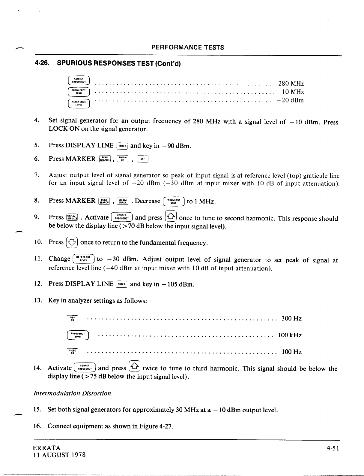
Page 449, Paragraph 4-26:
Replace pages 449 through 4-54 with attached
pages 449 through 4-54.
Section V
Page 5-79, Paragraph 5-28:
In second line of Step 11, change A7Jl to AlOJ2. Connection is shown correctly in Figure 5-42.
Page 5-93, Paragraph 5-32:
In Step 14, change 20.00 msec to 20.0 msec and kO.01 msec to kO.l msec.
Section VI
Page 6-32, Table 6-2:
Change Al A6R2 as follows:
AlA6R2,0757-0403,
1, RESISTOR 121 1% .125W F TC=O+lOO, 24546, C4-l/8-TO-12lR-F.
Page 6-48, Table 6-2:
Change A3A5Ul and A3A5U18 entries as follows:
A3A5U1, 1816-1129(CD=8), 1, IC-ROM 32 X 8,28480, 1816-1129.
A3A5U18,1816-113O(CD=l), 1, IC-ROM 32 X 8,28480,1816-1130.
Page 649, Table 6-2:
Change A3A6U4 through A3A6Ull entries as follows:
A3A6U4,1816-1131(CD=2), 1, IC-ROM 512 X 8,28480, 1816-1131.
A3A6U5,1816-1133(CD=4), 1, IC-ROM 512X 8,28480,1816-1133.
A3A6U6, 1816-1136(CD=7), 1, IC-ROM 512 X 8,28480, 1816-1136.
A3A6U7, 1816-1127(CD=6), 1, IC-ROM 512X 8, 28480, 1816-1127.
A3A6U8,1816-1134(CD=5), 1, IC-ROM 512 X 8,28480, 1816-1134.
A3A6U9,1816-1135(CD=6), 1, IC-ROM 512 X 8,28480,1816-1135.
A3A6UlO,1816-1128(CD=7), l,IC-ROM 512X8,28480,1816-1128.
A3A6U11, 1816-1132(CD=3), 1, IC-ROM 512 X 8,28480, 1816-1132.
Page 6-78, Table 6-2:
Change A4A7C6, C14, C23, C32, and C41 as follows:
A4A6C6, C14, C23, C32, C41,0121-0446,5, CAPACITOR-V TRMR CER 4.5-20PF 16OV PC-MTC, 28480,
0121-0446.
)Page 6-85, Table 6-2:
Change HP Part Number and Mfr Part Number of A4A8Y 1 -Y2 to 041 O-l 029.
2
HEWLETT

Model 8568A
08568-90012
~ ,-
ERRATA (Cont’d)
Volume 2 (Cont’d)
DPage 6-9 1, Table 6-2 :
Change HPPart Number and Mfr Part Number of ASAlJl to 1251-5549.
)Page 6-106, Table 6-2:
Change A13CR6 entry as follows:
A13CR6,1901~518,2, DIODE-SCHOTTKY, 28480,1901-0518.
)Page 6-108 and 6-109, Table 6-2:
Add a second Al4 entry as follows:
Al4 (OPTION OOl), 85680&0124 (CD=l), 1, BOARD ASSEMBLY, MEMORY, OPTION 001,28480,85680-60124.
Add a second A14Ul entry as follows:
A14Ul (OPTION OOI), 18184853 (CD=7), 1, IC-ROM 16K, OPTION 001 ONLY, 28480, 1818-0853.
Add a second A14U29 entry as follows:
A14U29 (OPTION OOl), 1818-0852 (CD=6), 1, IC-ROM 16K, OPTION 001 ONLY, 28480,1818-0852.
Page 6-120, Table 6-2:
Change A20C14 entry to read: “A20C14, NOT ASSIGNED”.
Change A20Ql entry as follows:
A20Q1,
Change A20R14 entry as follows:
A20R14.0698-8812, 1, RESISTOR 1 1% .125W F TC=OklOO, 28480,0698-8812.
Change A20R15 entry as follows:
A20Rl5,0698-3441,3, RESISTOR 215 1% .125W F TC=O*lOO, 24546, C4-l/B-TO-215R-F.
1854-0378, 1, TRANSISTOR Nl’N SI TO-39 PD=800MW, 01921,2N5 109.
Page 6-l 2 1, Table 6-2 :
Change A20Ul entry as follows:
A20Ul,O955-0084, 1, MIXER, DOUBLE-BALANCED, 28480,0955-0084.
Page 6-128, Table 6-2:
Add A23FLl entry after A23ATl as follows:
A23FL1,08568-60119 (CD=5), 1, FILTER, LOW-PASS 3.8 GHz, 1 l-POLE, 28480,08568-60119.
)Change A23A3AlQl HP Part Number to 50864201 and Mfr Part Number to TC-21A.
kPage 6-129, Table 6-2 :
Change A23A3A3Ql HP Part Number to 50864201 and Mfr Part Number to TC-21A.
Page 6-l 3 1, Table 6-2 :
Add A24El6 as follows:
A24E16,9170-0029, 1, SHIELDING BEAD (FOR BASE OF Q4), 28480.9170-0029.
Page 6-l 34, Table 6-2:
Change A25C1, C3 and C5 HP Part Number and Mfr Part Number to 0170-0064. (Change voltage in Description
to 100 VDC.)
Page 6-137, Table 6-2:
Add the following entries at the bottom of the page.
A27,85680-60095,1, FREQUENCY STANDARD 10 MHZ (INCLUDES TOP AND BOTTOM MOUNTS, ISOLATION
MOUNTS, CABLE ASSEMBLY A27W1, AND XTAL OSC A27Al), 28480,85680-60095.
A27W1,85680-60089, 1, CABLE ASSEMBLY, OSC OVEN POWER, 28480,85680-60089.
A27A1,0960-0477, 1, OSCILLATOR-XTAL 10 MHz, 28480,0960-0477.
ku3wL.m~ IFPACKARD
Ml
08568-90012 Model 8568A
ERRATA (Cont’d)
Volume 2 (Cont’d)
Page 6-138, Table 6-3:
Change second F 1 entry as follows:
Fl, 2110-0002,1, FUSE 2A 250V FAST-BLOW, 047OC, 312002
Page 6-140, Table 64:
Change second Fl entry as follows:
F I,2 l lO-0002,1, FUSE 2A 250V FAST-BLOW, 047OC, 3 12002
Change W4 to read: “NOT ASSIGNED”.
Page 6-141, Table 64:
Change Information card entries as follows:
85680-90029,1, INFORMATION CARD, FRONT PANEL OPERATION, ENGLISH, 28480,85680-90029
85680-90030. 1, INFORMATION CARD, REMOTE OPERATION, ENGLISH, 28480,85680-90030
85680-9003 1 , 1, INFORMATION CARD, FRONT PANEL OPERATION, JAPANESE, 28480,85680-90031
85680-90032,1, INFORMATION CARD, REMOTE OPERATION, JAPANESE, 28480,85680-90032
85680-90033,1, INFORMATION CARD, FRONT PANEL OPERATION, FRENCH, 28480,85680-90033
85680-90034,1, INFORMATION CARD, REMOTE OPERATION, FRENCH, 28480,85680-90034
Section VII
Page 7-l/7-2:
Replace with attached new pages 7-l/7-IA, 7-lB/7-2.
Page 7-l l/7-12:
Replace with attached new pages 7-l l/7-12.
Volume 3
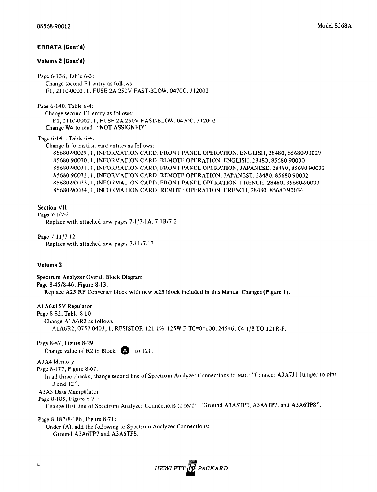
Spectrum Analyzer Overall Block Diagram
Page 8451846, Figure 8-13:
Replace A23 RF Converter block with new A23 block included in this Manual Changes (Figure 1).
Al A651 5V Regulator
Page 8-82, Table 8-10:
Change Al A6R2 as follows:
AlA6R2,0757-0403, 1, RESISTOR 121
Page 8-87, Figure 8-29:
Change value of R2 in Block @
A3A4 Memory
Page 8-177, Figure 8-67:
In all three checks, change second line of Spectrum Analyzer Connections to read:
3 and 12”.
A3A5 Data Manipulator
Page 8-l 85, Figure 8-7 1:
Change first line of Spectrum Analyzer Connections to read:
to 12 1,
1% .125W F TC=O+lOO, 24546, C4-l/8-TO-12lR-F.
“Connect A3A7Jl Jumper to pins
“Ground A3A5TP2, A3A6TP7, and A3A6TP8”.
Page 8-187/8-188, Figure 8-71:
Under (A), add the following to Spectrum Analyzer Connections:
Ground A3A6TP7 and A3A6TP8.

Model 8568A
08568-90012
-
ERRATA (Cont’d)
Volume 3 (Cont’dl
Page 8-190, Table 8-25:
Change A3AWl and A3AW18 entries as follows:
A3A5U1, 1816-1129(CD=8), 1, K-ROM 32 X 8,28480, 1816-1129.
A3A5U18, 1816-113O(CD=l), 1, K-ROM 32 X 8,28480, 1816-1130.
Page 8-19 1, Figure 8-74:
In Block 0 , add pin 8 (GROUND) to U16.
In Block
move level indicator symbol from pin 15 to pin 14 of U24.
@
In Block @ :add pin 12 to output of U21A.
A3A6 Main Control
Page 8-195, Figure 8-75:
In lower right corner of diagram, change line above
“REFER TO MANUAL” to read: “Verify 5 Vdc of P545 and activity
at U 16 pins 7 and 10; 7 = stable, 10 = unstable”.
Page 8-196, Figure 8-75:
Change second line of Spectrum Analyzer Connections for TEST A CHECK to read: “Connect A3A7Jl
pins 5 and 10”.
Page 8-198, Table 8-26:
Change A3A6U4 through A3A6Ull entries as follows:
A3A6U4,1816-1131(CD=2), 1, IC-ROM 512 X 8,28480, 1816-1131.
rcL A3A6U5,1816-1133(CD=4), 1, IC-ROM 512 X 8,28480, 1816-1133.
A3A6U6, 1816-1136(CD=7), 1, IC-ROM 512 X 8,28480, 1816-1136.
A3A6U7,1816-1127(CD=6), 1, IC-ROM 512 X 8,28480, 1816-1127.
A3A6U8,1816-1134(CD=5), 1, IC-ROM 512 X 8,28480, 1816-1134.
A3A6U9,1816-1135(CD=6), 1, IC-ROM 512 X 8,28480, 1816-1135.
A3A6U10, 1816-1128(CD=7), 1, IC-ROM 512 X 8,28480, 1816-1128.
A3A6Ul1, 1816-1132(CD=3), 1, IC-ROM 512 X 8,28480, 1816-1132.
Jumper to
Page 8-199, Figure 8-78:
In Block @ , connect D GND to GND 1 and change Cl-Cl 1 to ClC6, C8-Cl1 and value to O.lUF.
In Block
, add C7,O.lUF, in parallel with R6.
Q
A3A7 Interface
Page 8-203, Figure 8-79:
Change secand line of Spectrum Analyzer Connections under DECODER CHECK to read: “Connect A3A7Jl Jumper to
pins 7 and 8”.
Page 8-204, Figure 8-79:
Change first line of Spectrum Analyzer Connections for IDB INTERFACE CHECK (ADDRESS) to read: “Connect
A3A7Jl Jumper to pins 6 and 9”.
Change first line of Spectrum Analyzer Connections for IDB INTERFACE CHECK (DATA) to read: “Connect A3A7Jl
Jumper to pins 7 and 8”.
Page 8-207, Figure 8-82:
In Block , add pin 14 to +5VF connection of U12A.
In Block , add NC to pins 6 and 10 of U? and show pin 9 connected to ground.
In Block change connections to UZl control block as follows: pins 1,9, 7, and 10 to pin 16 (+5VF), pin 2 to
UlOF pin
12, omit all other connections. Change connections to U20 control block as follows: pin 1 to U18B (TPlO)
inBlock @ ,pinZtoU21 pin 12,pins9,7,and IOtopin 16(+5VF).
HEWLETT -$-PACKARD
Al
5

08568-90012 Model 8568A
ERRATA (Cont’d)
Volume 3 (Cont’d)
A3A8 Analog-Digital Converter
Page 8-2 15, Figure 8-89:
Change first line in Spectrum Analyzer Connections for TEST A CHECK to read: “Connect A3A7Jl Jumper to pins
5 and 10”.
Change first line in Spectrum Analyzer Connections for AD,C CHECK to read: “Connect A3A7Jl Jumper to pins 2 and
13”.
Page 8-22 1, Figure 8-92:
In Block @ ,
add +15VFl between L4 and C6.
In Block * , reverse pins Q 2 and 3 and pins 4 and 8 of U 12. Change power supply connection of U8 to +5VF 1.
In Block @ , change voltage of U15 to 6.95V. Change filter capacitor C8 for U6 to C9.
A4A7 3 MHz Bandwidth Filter
Page 8-321, Table 8-45:
Change A4A7C6, C14, C23, C32, and C41 as follows:
A4A6C6, C14, C23, C32, C41,0121-0446,5, CAPACITOR-V TRMR CER 4.5-20PF 160V PC-MTG, 28480,
0121-0446.
Page 8-329, Figure 8-146:
Change value of C6, C14, C23, C32, and C41 to 4.5-20PF (located top right of each block).
bA4A8 Attenuator-Bandwidth Filter
Page 8-342, Table 847 :
Change HP Part Number and Mfr Part Number of A4A8Y 1 -Y2 to 04 10-l 029.
Volume 4
RF Section Repair Procedures
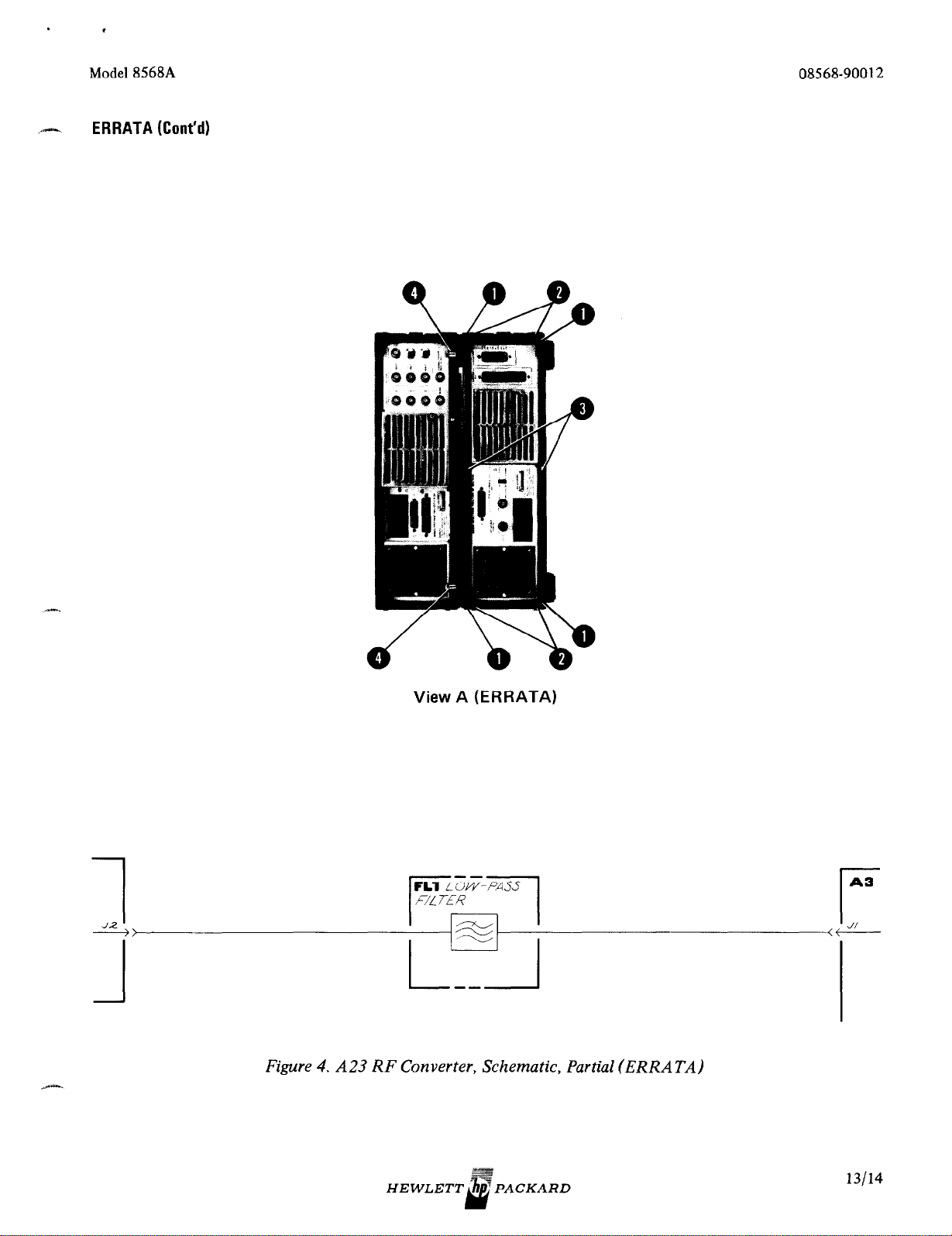
Page 9-2119-22, Figure 9-7, Front Panel Removal and Repair:
Add Step 2a as follows: “2a. Loosen thumbscrews
Change Step 4 to read: “4. Remove covers from top and bottom of RF Section by loosening screws
Q
.”
8
Change Step 5 to read: “5. Separate instruments by holding IF-Display Section in place while pushing the RF Section
at the front panel.”
Replace View A with the View A (ERRATA) contained in this Manual Changes package.
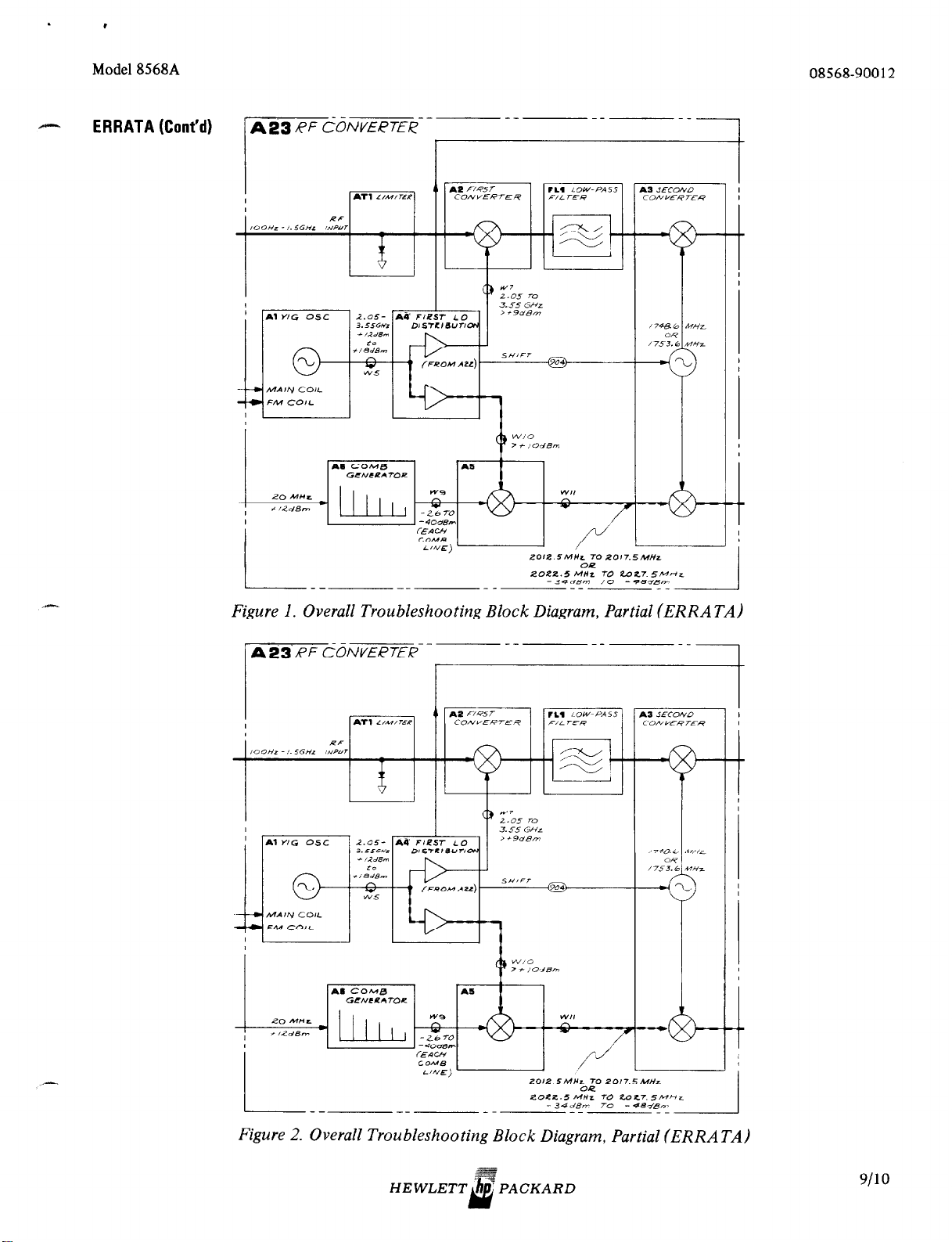
Spectrum Analyzer Overall Block Diagram
Page 94319-44, Figure 9-13:
Replace A23 RF Converter block with new A23 block included in this Manual Changes (Figure 2).
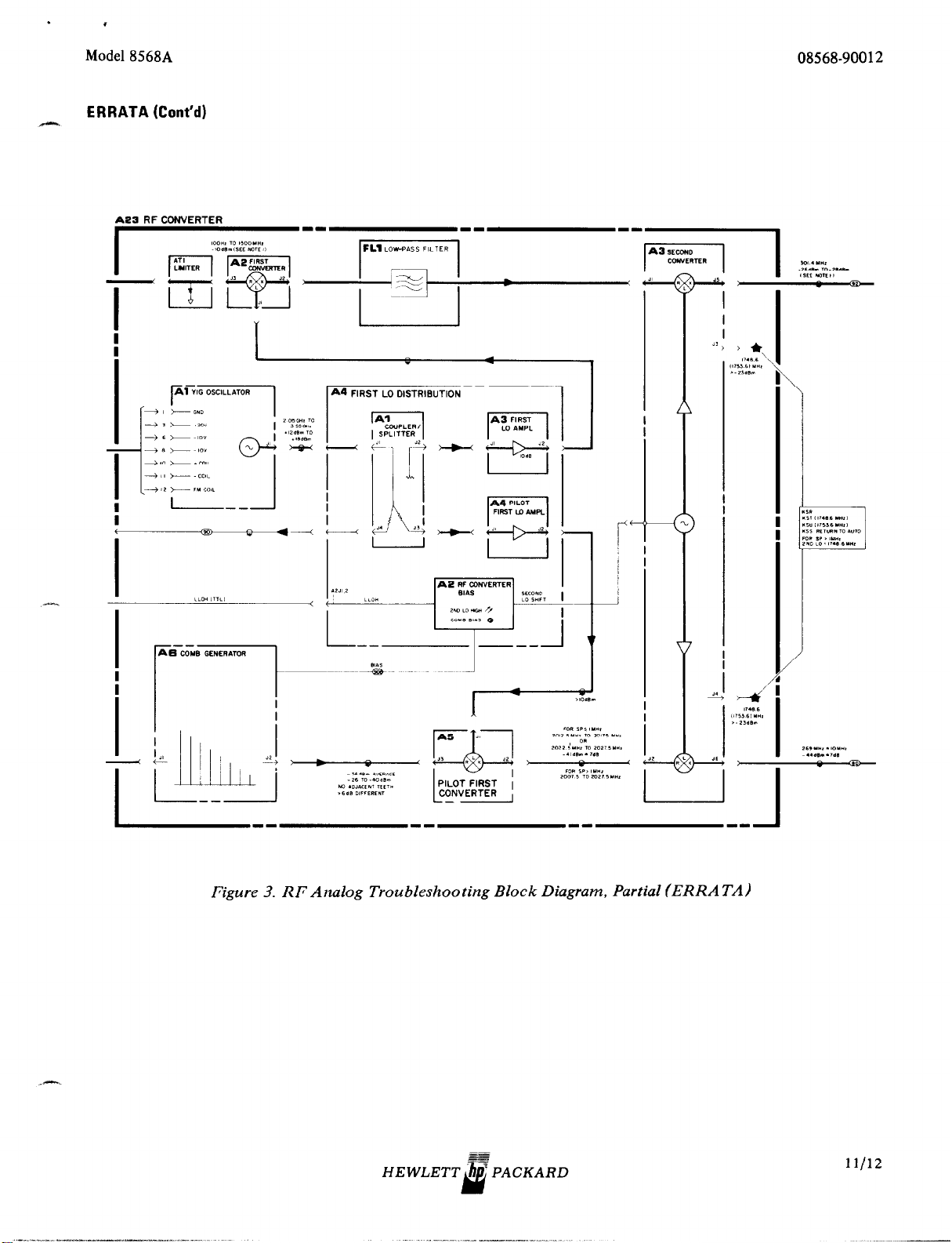
RF Analog Troubleshooting Block Diagram
Page 9-55/9-56, Figure 9-15:
Replace A23 RF Converter block with new A23 block included in this Manual Changes (Figure 3).
.”
)A5 Front Panel
Page 9-67, Table 9-4:
Change HP Part Number and Mfr Part Number of ASAlJl to 1251-5549.
6
HEWLETT

.
t
Model 8568A 08568-90012
ERRATA (Cont’d)
Volume 4 (Cont’d)
Al2 RF Section
Interface
Page 9-129, Fi ure 944:
change control block inputs to Ul as follows: pin 6 to 4, pin 7 to 2, and pin 9 to 1.
In Block
Q
,
)A13 HP-IB Interface
Page 9-138, Figure 945:
PI-1 GND should connect to Jl-1 GND. PI-19 should be labeled NC.
Page 9-139, Step 1:
Change 200 ns in sixth line to 200 ms.
Page 9-140, Step 2:
Change 50 ps in first line to 50 ns.
Change 15 fis in second line to 15 ns.
Page 9-143, Table 9-18:
Change A13CR6 entry as follows:
A13CR6,1901-0518,2, DIODE-SCHOTTKY, 28480,1901-0518
- )A14 Memory
Page 9-159 and g-160, Table 9-19:
Add a second Al4 entry as follows:
A14 (OPTION OOl), 8568040124 (CD=l), 1, BOARD ASSEMBLY, MEMORY, OPTION 001,28480,85680-60124.
Add a second A14Ul entry as follows:
A14Ul (OPTION OOI), 1818a853 (CD=7), 1, IC-ROM 16K, OPTION 001 ONLY,28480,1818-0853.
Add a second A14U29 entry as follows:
A14U29 (OPTION 001) 1818-0852 (CD=6), 1, IC-ROM 16K, OPTION 001 ONLY,28480,1818-0852.
.II.
Page g-161/9-162, Figure 9-53:
Add P2 signatures for Option 001 as follows:
P2-8, C79P
F2-24,170l
P2-9,9U6U P2-25, CFP3
P2-10,27HO P2-26,980U
P2-11, AP4P P2-27, II4AF
P2-12, FC22 P2-28,529C
P2-13,8U45
P2-29, cu99
P2-14,9373
Under (C) SA TRIGGER CHECK, delete last line of Signature Analyzer Connections (POD GROUND to A15TP8) and
add under Spectrum Analyzer Connections, Ground Al 5TP8, PRESS INSTR PRESET.
Page g-167/9-168, Figure 9-56 (2 of 2):
In Block 0 , add the following note above Ul :
“I-J1 and U29 contain a different program for Option 001 (75a).”

08568-90012
ERRATA (Cont’d)
Volume 4 (Cont’d)
A20 Third Converter
Page 9-227, Table 9-3 1:
Change A20C 14 entry to read: “A20C 14, NOT ASSIGNED”.
Change A20Ql entry as follows:
A20Q1, 1854-0378, 1, TRANSISTOR NPN Sl TO-39 PD=800MW, 28480,1854-0378.
Change A20R14 entry as follows:
A20Rl4,0698-8812, I, RESISTOR 1 1% .125W F TC=O?lOO, 28480,0698-8812.
Change A20Rl.5 entry as follows:
A20Rl5,0698-3441,3, RESISTOR 215 1% .125W F TC=O?lOO, 24546, C4-l/8-TO-215R-F.
Page 9-228, Table 9-3 1:
Change A20Ul entry as follows:
A20Ul,O955-0084, I, MIXER, DOUBLE-BALANCED, 28480,0955-0084.
Page 9-22919-230, Figure 9-77:
Delete Cl4 (located at lower right corner of Ul).
Page 9-23 l/9-232, Figure 9-79, A20 Schematic:
Model 8568A
In Block @ , delete C14.
In Block @ ,
A23 RF Converter
Page 9-264, Table 9-37:
Add A23FLl entry after A23ATl as follows:
A23FL1,08568-60119 (CD=5), 1, FILTER, LOW-PASS 3.8 GHz, 1 l-POLE, 28480,08568-60119.
)Change A23A3AlQl HP Part Number to 5086-4201 and Mfr Part Number to TC-21A.
)Page 9-265, Table 9-37:
Change A23A3A3Ql HP Part Number to 50864201 and Mfr Part Number to TC-21A.
Page 9-27319-274, Figure 9-96:
Replace Figure 9-96 with attached Figure 9-96 (ERRATA).
Page 9-27519-276, Figure 9-97:
Add the attached partial diagram (Figure 4) to Figure 9-97 showing the replacement of W4 with A23FLI.
A24 Voltage Regulator
Page 9-279. Table 9-38:
Add A24E 16 as follows:
A24El6,9170-0029,1, SHIELDING BEAD (FOR BASE OF Q4), 28480,9170-0029.
change value of R 14 to 1 ohm and value of R 15 to 2 15.
Page 9-285, Figure 9-99:
Add shielding bead El6 to base of Q4 in Block
A25 Rectifier
Page 9-288. Table 9-40:
Change A25C 1, C3 and C5 HP Part Number and Mfr Part Number to 0170-0064. (Change voltage in Description to
100 VDC.)
8
@ .
HEWLETT FPACKARD
Al
.
I
Model 8568A
-
ERRATA (Cont’d)
/-RFCONYEPTER--, -- -- ---i
I
I
08568-90012
t
Figure 1. Overall Troubleshooting Block Diagram, Partial (ERRATA)
Figure 2. Overall Troubleshooting Block Diagram, Partial (ERRATA)
HEWLETT &4CKARD
iha
9/10
.
,
Model 8568A
ERRATA (Cont’d)
A23 RF CONVERTER
08568-90012
I I
A4 FIRST LO DISTRIBUTION - -
I
I
Figure 3. RF Analog Troubleshooting Block Diagram, Partial (ERRATA)
HEWLETT ~‘PACKARD
hi
1 l/12
Model 8568A
08568-90012
-
ERRATA (Cont’d)
View A (ERRATA)
Figure 4. A23 RF Converter, Schematic, Partial (ERRATA)
A3
r
i&
13114
HEWLETT PACKARD
OPERATING AND SERVICE MANUAL
8568A
SPECTRUM ANALYZER
100 Hzto1.5 GHz
(Including Options 001, 080, 081, 400, 907, 908, 909,and 910)
SERIAL NUMBERS
This manual applies directly to Model 8568A RF Sections
with serial numbers prefixed 1839A and IF-Display Sections with serial numbers prefixed 1838A.
With changes described in Section VII (Volume 2), this
manual also applies to RF Sections with serial numbers
prefixed 1837A, 1828A, 1824A, 1818A, 1812A, 1806A,
1803A, 1743A, 1740A, and 1721A and to IF-Display
Sections with serial numbers prefixed 1833A, 1826A,
1823A, 1820A, 1811A, 1805A, 1745A, and 1721A.
For additional information about serial number coverage,
refer to INSTRUMENTS COVERED BY MANUAL in
Section I and MANUAL BACKDATING CHANGES in
Section VII.
@Copyright
1400 FOUNTAIN GROVE PARKWAY, SANTA ROSA, CALIFORNIA 95404, U.S.A.
HEWLETT-PACKARD COMPANY
1978
MANUAL PART NO.
Refer to following page.
Printed: JUNE 1978
HP 8568A SPECTRUM ANALYZER
SERVICE DOCUMENTATION SUMMARY
The HP 8568A service documentation comprises several individual manuals.
These manuals may be ordered individually or in combination as follows:
1) Operating and Service Manual (includes
items 2 and 3)
2)
Operation
3) Remote Operation
4) Operation Verification (includes tape
cartridge and operation supplement)
08568-90012
08568-90002
08568-90003
08568-60002

SECTION I
GENERAL INFORMATION
l-l.
1-2. This Operating and Service manual contains
information required to install, operdte, test, ad-
just, and service the Hewlett-Packard Model
8568A Spectrum Analyzer. Figure 1-l shows the
instrument and accessories supplied. This section
covers instrument indentification, description, options, accessories, specifications, and other basic
information.
1-3. This manual is divided into four volumes
and nine sections as follows:
Volume 1
SECTION I, GENERAL INFORMATION;
contains the instrument description and
specifications, explains accessories and options,
and lists recommended test equipment.
SECTION I I,
OPERATION VERIFICATION; contains in-
formation concerning initial mechanical inspection, verification of electrical operation,
preparation for use, operating environment,
and packing and shipping.
SECTION III, OPERATION; contains detailed
operating instructions for both manual frontpanel and HP-IB remote operation and in-
formation.
Volume 2
SECTION IV, PERFORMANCE TESTS; contains the necessary tests to verify that the electrical operation of the instrument is in accordance with published specifications.
INTRODUCTION
INSTALLATION AND
SECTION VII, MANUAL BACKDATING
CHANGES; contains backdating information
to make this manual compatible with earlier
equipment configurations.
Volume 3
SECTION VIII, IF-DISPLAY SECTION SERVICE; contains schematic diagrams, block
diagrams, component location illustrations, circuit description, repair procedures, and
troubleshooting information for the IF-Display
Section of the instrument.
Volume 4
SECTION IX, RF SECTION SERVICE ; contains
schematic diagrams, block diagrams, component
location illustrations, circuit descriptions, repair
procedures, and troubleshooting information for
the RF Section of the instrument.
l-4. SPECIFICATIONS
1-5. Instrument specifications are listed in
Table l-l. These specifications are the per-
formance standards or limits against which
the instrument is tested. Table l-2 lists FLIPplemental
characteristics are not specifications but are
typical characteristics included as additional
information for the user.
I-5a.
DARD INSTRUMENT)
l-5b. Manual
l-5b-1. In frequency spans < 1 MHz (when the
analyzer is phase-locked) the YTO UNLOCK
Message is displayed on the CRT whenever the
ten ter
characteristics.
KNOWN
frequency is
FIRMWARE “BUGS’ (STAN-
Operation
Supplemental
changed from
SECTION V, ADJUSTMENTS; contains the
necessary adjustment procedures to properly
adjust the instrument after repair.
SECTION VI, REPLACEABLE PARTS; contains the information necessary to order parts
and/or assemblies for the instrument.
ERRATA
10 OCTOBER 1978
@@@aMHztoQQ@@Hz
using either the DATA control knob or the step
keys. In other words between any frequency
ending in 7 where the preceding digit is odd to
any frequency ending in 8 where the preceding
digit is odd. The first two digits are unimportant.
For example, between 1017 MHz and 1018 MHz.
l-l


 Loading...