

Page 1
Keysight W6600A-Series
LPDDR4 BGA Interposers
Installation Guide
Page 2

Notices
CAUTION
WARNING
© Keysight Technologies 2016, 2017
No part of this manual may be reproduced in
any form or by any means (including electronic storage and retrieval or translation
into a foreign language) without prior agreement and written consent from Keysight
Technologies as governed by United States
and international copyright laws.
Manual Part Number
W6601-97000
Edition
Second Edition, August 2017
Available in electronic format only
Keysight Technologies
1900 Garden of the Gods Road
Colorado Springs, CO 80907 USA
Warranty
THE MATERIAL CONTAINED IN THIS DOCUMENT IS PROVIDED "AS IS," AND IS SUBJECT TO BEING CHANGED, WITHOUT
NOTICE, IN FUTURE EDITIONS. FURTHER,
TO THE MAXIMUM EXTENT PERMITTED BY
APPLICABLE LAW, KEYSIGHT DISCLAIMS
ALL WARRANTIES, EITHER EXPRESS OR
IMPLIED WITH REGARD TO THIS MANUAL
AND ANY INFORMATION CONTAINED
HEREIN, INCLUDING BUT NOT LIMITED TO
THE IMPLIED WARRANTIES OF MERCHANTABILITY AND FITNESS FOR A PARTICULAR
PURPOSE. KEYSIGHT SHALL NOT BE LIABLE
FOR ERRORS OR FOR INCIDENTAL OR CONSEQUENTIAL DAMAGES IN CONNECTION
WITH THE FURNISHING, USE, OR PERFORMANCE OF THIS DOCUMENT OR ANY
INFORMATION CONTAINED HEREIN.
SHOULD KEYSIGHT AND THE USER HAVE A
SEPARATE WRITTEN AGREEMENT WITH
WARRANTY TERMS COVERING THE MATERIAL IN THIS DOCUMENT THAT CONFLICT
WITH THESE TERMS, THE WARRANTY
TERMS IN THE SEPARATE AGREEMENT WILL
CONTROL.
Technology Licenses
The hardware and/or software described in
this document are furnished under a license
and may be used or copied only in accordance with the terms of such license.
U.S. Government Rights
The Software is "commercial computer software," as defined by Federal Acquisition
Regulation ("FAR") 2.101. Pursuant to FAR
12.212 and 27.405-3 and Department of
Defense FAR Supplement ("DFARS")
227.7202, the U.S. government acquires
commercial computer software under the
same terms by which the software is customarily provided to the public. Accordingly,
Keysight provides the Software to U.S. government customers under its standard commercial license, which is embodied in its
End User License Agreement (EULA), a copy
of which can be found at
sight.com/find/sweula
forth in the EULA represents the exclusive
authority by which the U.S. government may
use, modify, distribute, or disclose the Software. The EULA and the license set forth
therein, does not require or permit, among
other things, that Keysight: (1) Furnish technical information related to commercial
computer software or commercial computer
software documentation that is not customarily provided to the public; or (2) Relinquish
to, or otherwise provide, the government
rights in excess of these rights customarily
provided to the public to use, modify, reproduce, release, perform, display, or disclose
commercial computer software or commercial computer software documentation. No
additional government requirements beyond
those set forth in the EULA shall apply,
except to the extent that those terms, rights,
or licenses are explicitly required from all
providers of commercial computer software
pursuant to the FAR and the DFARS and are
set forth specifically in writing elsewhere in
the EULA. Keysight shall be under no obligation to update, revise or otherwise modify
the Software. With respect to any technical
data as defined by FAR 2.101, pursuant to
FAR 12.211 and 27.404.2 and DFARS
227.7102, the U.S. government acquires no
greater than Limited Rights as defined in
FAR 27.401 or DFAR 227.7103-5 (c), as
applicable in any technical data.
http://www.key-
. The license set
Safety Notices
A CAUTION notice denotes a hazard. It
calls attention to an operating procedure, practice, or the like that, if not
correctly performed or adhered to,
could result in damage to the product
or loss of important data. Do not proceed beyond a CAUTION notice until
the indicated conditions are fully
understood and met.
A WARNING notice denotes a hazard.
It calls attention to an operating procedure, practice, or the like that, if not
correctly performed or adhered to,
could result in personal injury or
death. Do not proceed beyond a
WARNING notice until the indicated
conditions are fully understood and
met.
2 Keysight W6600A-series LPDDR4 BGA Interposers Installation Guide
Page 3

In This Guide
This document provides installation information for the following Keysight products:
W6601A LPDDR4 BGA Interposer, 200-ball, 2-wings
U4208A 61-pin ZIF from left wing probe/cable (160 pin direct connect to LA).
This probe/cable is for use with the W6601A interposer.
U4209A 61-pin ZIF from right wing probe/cable (160 pin direct connect to LA)
This probe/cable is for use with the W6601A interposer.
W6602A LPDDR4 RC BGA Interposer, 200-ball, rigid
U4207A Zero ohm, 34 channels, Soft Touch Pro, single-ended probe/cable (160 pin direct connect to LA)
This probe/cable is for use with the W6602A interposer.
Keysight W6600A-series LPDDR4 BGA Interposers Installation Guide 3
Page 4

4 Keysight W6600A-series LPDDR4 BGA Interposers Installation Guide
Page 5

Contents
1 Introduction to W6600-Series Interposers
2 Introduction to W6601A LPDDR4 BGA Interposer
In This Guide 3
Compatibility with Logic Analyzer Modules 9
W6601A LPDDR4 BGA Interposer, 200-ball, 2-wings 12
Software Configurations 12
W6601A Technical Features Summary 13
W6601A Riser 13
U4208A 61-pin ZIF Probe / Cable (for Left Wing) 14
U4209A 61-pin ZIF Probe / Cable (for Right Wing) 15
Hardware and Software Requirements 16
Mechanical Considerations 18
W6601A Interposer Dimensions 18
W6601A Riser Dimensions 19
W6601A Keep-Out Volume 19
3 Introduction to W6602A LPDDR4 BGA Interposer
W6602A LPDDR4 RC BGA Interposer, 200-ball, Rigid 22
Software Configurations 23
W6602A Technical Features Summary 24
W6602A Riser 24
U4207A Zero ohm, 34 channels, Soft Touch Pro, Single-ended Probe/Cable 25
Hardware and Software Requirements 26
Mechanical Considerations 28
W6602A Interposer Dimensions 28
W6602A Riser Dimensions 29
4 W6600A-Series Interposers and Riser Soldering Guidelines
Recommended Soldering Guidelines 33
Soldering Steps 34
Interposer Fabrication Notes 36
Keysight W6600A-series LPDDR4 BGA Interposers Installation Guide 5
Page 6

Contents
5 Setting up the W6601A Interposer
W6601A Interposer Setup - Overview 38
Step 1 - Soldering the W6601A Interposer 39
Step 2 - Connecting the W6601A Interposer to U4208A and U4209A Probe Cables 40
W6601A Interposer Wings Pinout 41
Step 3 - Connecting the U4208A and U4209A Probe Cables to a U4164A Logic
Analyzer 43
Logic Analyzer Channels to Signals Mapping 43
Signals not probed by the Logic Analyzer 45
6 Setting up the W6602A Interposer
W6602A Interposer Setup - Overview 48
Step 1 - Soldering the W6602A Interposer 49
Step 2 - Making Clock Qualifier Connections 50
W6602A Clock Connectors 50
U4207A Flying Leads Orientation 51
Step 3 - Connecting the W6602A Interposer to U4207A Probes 53
Step 4 - Connecting the U4207A Probe Pods to the Logic Analyzer Module Pods 54
For Two 16-bit Channels DRAM Configuration 54
For a Single 32-bit Channel DRAM Configuration 56
W6602A Interposer Footprints Pinout 58
W6602A Clock Connectors Pinout 59
W6602A Clock Qualifier and RESET Connections 60
Logic Analyzer Channels to Signals Mapping 61
Signals not probed by the Logic Analyzer 62
7 Setting Up the Logic Analyzer for W6600A-series Interposers
Before You Start 64
Loading a Configuration File 65
To save a configuration file 65
Troubleshooting Problems with Thresholds and Sample Positions Setup 66
8 Making Power Integrity Measurements using W6600A Series Interposers
Overview 68
Power Integrity Measurement Setup 68
6 Keysight W6600A-series LPDDR4 BGA Interposers Installation Guide
Page 7

W6600A-Series Interposers Power Filter Capacitors 69
W6601A Power Filter Capacitors 69
W6602A Power Filter Capacitors 70
Correlating Power Integrity Measurements with Memory Analysis Measurements 71
9 Characteristics, Regulatory, Safety and Storage Information
Operating Characteristics 74
Storage, Inspection, Baking, and Cleaning Guidelines 75
Guidelines for Shelf Life and Solder-ability of W6600A-series Interposers 75
Cleaning of W6601A Interposer Gold Fingers 75
Regulatory Notices 76
WEEE Compliance 76
China RoHS 76
Index
Contents
Keysight W6600A-series LPDDR4 BGA Interposers Installation Guide 7
Page 8

Contents
8 Keysight W6600A-series LPDDR4 BGA Interposers Installation Guide
Page 9

Keysight W6600A-series LPDDR4 BGA Interposers
NOTE
Installation Guide
1 Introduction to W6600-Series
Interposers
The W6600A-series LPDDR4 BGA Interposers enable probing of 200-pin JEDEC standard footprint
directly at the ball grid array using the Keysight U4164A logic analyzer. These interposers provide
you:
• single touch probing of DQ signals
• capture of CA, Control, and DQ signals at data rates tested up to 3200MT/s.
• access to LPDDR4 DQ signals above 2.5Gb/s without double probe load by utilizing the Quad
Sampling features of a U4164A logic analyzer module.
A W6600A-series interposer interposes between the DRAM being probed and the PC board where
the DRAM would normally be soldered. The interposer is designed to be soldered to the PCB
footprint for the DRAM on top of either the LPDDR riser included with the W6600-series BGA
interposer or an optional Grypper socket (not included with the interposer) or both. The DRAM being
probed is then soldered to the top side of the interposer.
Each DRAM signal in the common footprint passes directly from the bottom side of the interposer to
the top side of the interposer.
Currently, in this series, Keysight provides the following interposers:
W6600A-series Interposer Description
W6601A LPDDR4 BGA Interposer,
200-ball, 2-wings
W6602A LPDDR4 RC BGA
Interposer, 200-ball, rigid
All probing including BGA interposers, become a part of the system under test when installed.
Maximum data rates and performance results will vary by systems under test, BGA rework, and
probing irregularities.
Compatibility with Logic Analyzer Modules
The W6600-series interposers are compatible with the Keysight U4164A AXIe-based logic analyzer
module.
All W6600A-series interposers are tested for via connections through the interposer and
signal trace connectivity to the wing connections.
A flexible interposer with two wings
Provides access to partial DQ signals and only one channel of CA signals on an LPDDR4 200
ball DRAM.
Refer to the chapter “Introduction to W6601A LPDDR4 BGA Interposer" on
page 11.
A rigid interposer
Provides access to all DQ and CA signals for both channels of an LPDDR4 200 ball DRAM.
Refer to the chapter “Introduction to W6602A LPDDR4 BGA Interposer" on
page 21.
Page 10

1 Introduction
10 Keysight W6600A-series LPDDR4 BGA Interposers Installation Guide
Page 11

Keysight W6600A-series LPDDR4 BGA Interposers
Installation Guide
2 Introduction to W6601A
LPDDR4 BGA Interposer
W6601A LPDDR4 BGA Interposer, 200-ball, 2-wings / 12
U4208A 61-pin ZIF Probe / Cable (for Left Wing) / 14
U4209A 61-pin ZIF Probe / Cable (for Right Wing) / 15
Hardware and Software Requirements / 16
Mechanical Considerations / 18
This chapter introduces the hardware components that are needed for the W6601A LPDDR4 BGA
interposer setup. It also lists the software requirements as well as describes the mechanical
considerations such as various dimensions and KOV that you should know before you start setting up
and using the W6601A interposer.
Page 12
2 Introduction to W6601A LPDDR4 BGA Interposer
2 Flex wings with
ZIF connectors
Pin 1 Marking
NOTE
W6601A LPDDR4 BGA Interposer, 200-ball, 2-wings
The W6601A interposer has two flexible wings, each with a set of fingers for Zero Insertion Force
(ZIF) connections that connect it to a U4208A or a U4209A 61-pin ZIF probe/cable. For the left wing
of the interposer, you use the U4208A probe/cable and for the right wing of the interposer, you use
the U4209A probe/cable. These cables are then connected to the U4164A Logic Analyzer module’s
pods.
The following figure shows a W6601A interposer’s top view.
Figure 1 W6601A Interposer
The W6601A interposer supports dual bank 16-bit data LPDDR4 200 ball DRAM that is being used as
a single 32-bit channel device. The interposer probes a subset of the DQ data lines of both banks of
such an LPDDR4 BGA 200 DRAM.
If the DRAM is used as two single x16 channel devices, then the W6601A interposer can
probe only CA signals from channel A.
This interposer is optimized to work with the U4164A logic Analyzer module to achieve higher data
rates with smaller KOV.
Software Configurations
The W6601A interposer can be used in the following three logic analyzer software configurations:
• 10 GHz Timing mode
• State mode under 2500 Mb/s (double edge clocking)
• State mode over 2500 Mb/s (single edge clocking)
This interposer effectively utilizes the single touch probing and quad sampling features of the
U4164A logic analyzer module thereby allowing you to probe LPDDR4 DQ signals above 2.5Gb/s
without double probe load. (In quad sampling, four samples are captured per clock edge at two
different thresholds. Two samples are taken at each threshold.)
12 Keysight W6600A-series LPDDR4 BGA Interposers Installation Guide
Page 13
For probing signals under 2.5Gb/s, you can use the W6601A interposer with the U4164A module’s
Pin 1 Marking
NOTE
dual clock edge clocking and dual sample mode instead of the quad sample mode. The U4164A
module’s dual sampling with dual thresholds allows you to capture separate Read and Write samples
per clock edge.
W6601A Technical Features Summary
• Probes a JEDEC LPDDR4 BGA 200 footprint. Maximum of 10 mm wide X 15 mm long LPDDR4
DRAM package can fit on top of the W6601A interposer without an additional riser or a socket to
provide clearance for the RC components.
• For the two flex wings of the interposer, the recommended bend radius is 2.5 mm (0.09") if flex is
bent at a rigid portion of the interposer.
• Logic analyzer connections are made using U4208A and U4209A ZIF probe cables. The
U4208A/U4209A ZIF connectors doors open on the top of the W6601A wings and away from
these wings.
• An isolation Tip Resistor (100 Ohms) and RC components network is present on the W6601A
interposer. No RC network present on the U4208A/U4209A probe cables. Also, there are no RCs
on the bottom of the interposer.
• Has a power plane and separate ground planes - 1.1 V (VDD2/VDDQ) and 1.8 V (VDD1).
• Also provides VDD and VDDQ power filter capacitors to allow you to make power integrity
measurements using the Keysight Power Rail probe and Infiniium S-series oscilloscope.
Introduction to W6601A LPDDR4 BGA Interposer 2
W6601A Riser
An LPDDR4 BGA 200 ball riser is provided with each W6601A interposer to allow the interposer to
clear surrounding devices. Optionally, you can use a Grypper socket. It is not provided with the
interposer.
The following figure displays a riser that is provided with the W6601A interposer.
Figure 2 Riser that accompanies the W6601A interposer
The LPDDR 200 ball riser includes ground planes for optimal signal integrity. Due to these
ground planes, the riser’s alignment with the DRAM should be such that the TOP side of the
riser must point towards the DRAM and the Pin 1 indicator on the riser must orient towards the
“A1” pin of the DRAM.
To know how to solder the riser to the W6601A interposer and PC board, refer to the chapter
“W6600A-Series Interposers and Riser Soldering Guidelines" on page 31.
Keysight W6600A-series LPDDR4 BGA Interposers Installation Guide 13
Page 14
2 Introduction to W6601A LPDDR4 BGA Interposer
Connector to connect
to the left flex wing of
the W6601A interposer
Two pods to connect
to the Logic Analyzer
pods
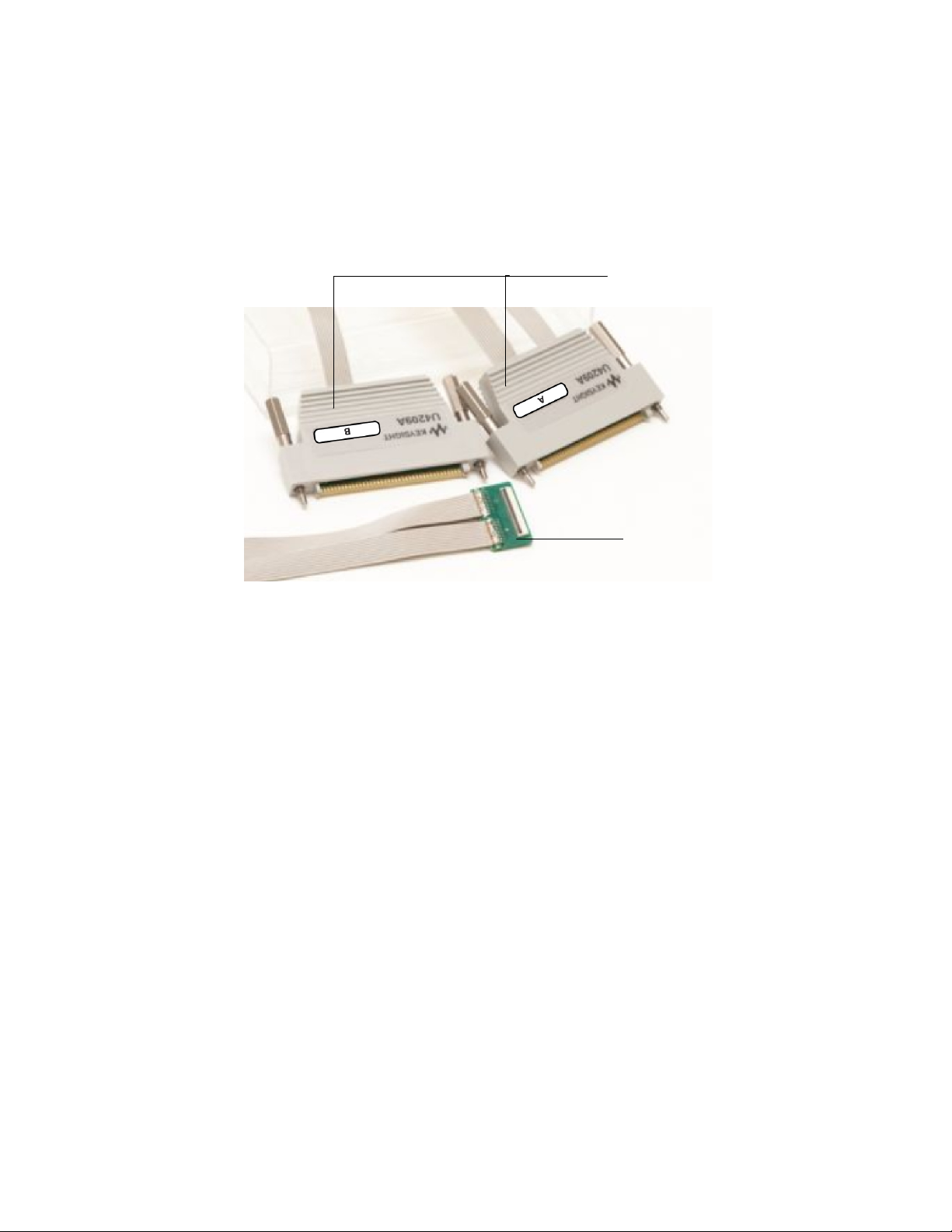
U4208A 61-pin ZIF Probe / Cable (for Left Wing)
One U4208A probe cable is required to connect a W6601A interposer’s left wing to a U4164A Logic
Analyzer module.
Figure 3 U4208A 61-pin ZIF probe cable
To know how to connect a W6601A interposer to a U4208A probe/cable, refer to the following topics
in this guide:
• “Step 2 - Connecting the W6601A Interposer to U4208A and U4209A Probe Cables" on page 40
To get information such as its characteristics, specifications, pinout, safety information, accessories,
and dimensions of the U4208A probe/cable, refer to the Keysight U4200A-Series Probes and Cables
User Guide (part number U4200-97000) available on www.keysight.com.
14 Keysight W6600A-series LPDDR4 BGA Interposers Installation Guide
Page 15
U4209A 61-pin ZIF Probe / Cable (for Right Wing)
Connector to connect to the right flex
wing of the W6601A interposer
Two pods to connect to the Logic
Analyzer pods
One U4209A probe cable is required to connect a W6601A interposer’s right wing to a U4164A Logic
Analyzer module.
Introduction to W6601A LPDDR4 BGA Interposer 2
Figure 4 U4209A 61-pin ZIF probe cable
To know how to connect a W6601A interposer with a U4209A probe/cable, refer to the topic:
• “Step 2 - Connecting the W6601A Interposer to U4208A and U4209A Probe Cables" on page 40
To get information such as its characteristics, specifications, pinout, safety information, accessories,
and dimensions of the U4209A probe/cable, refer to the Keysight U4200A-Series Probes and Cables
User Guide (part number U4200-97000) available on www.keysight.com.
Keysight W6600A-series LPDDR4 BGA Interposers Installation Guide 15
Page 16

2 Introduction to W6601A LPDDR4 BGA Interposer
Hardware and Software Requirements
Before you start installing the W6600A-series interposers, ensure that you have the following list of
hardware and software components needed for these interposers.
Hardware Requirements for W6601A
U4164A AXIe-based Logic Analyzer Module
M9502A 2-slot or M9505A 5-slot AXIe chassis to install the U4164A module
M9536A embedded controller or host PC with PCI express adapter card for the chassis
W6601A LPDDR4 Interposer(s)
U4208A 61-pin ZIF probe cables to connect the W6601A interposer to Logic Analyzer module
One cable needed for each interposer
U4209A 61-pin ZIF probe cables to connect the W6601A interposer to Logic Analyzer module
One cable needed for each interposer
Software Requirements Licensing Description
Logic and Protocol Analyzer software version 6.30 or
higher.
(Required)
B4661A Memory Analysis Software Tools Package
version 6.30 or higher. (Required)
The below-mentioned licensed/unlicensed software features from the B4661A software package are required for W6601A.
Default LPDDR configuration files
(Required)
DDR Setup Assistant and DDR Eyefinder software
version 6.30 or higher.
(Required)
DDR Custom Configuration Creator Tool version 6.30
or higher
(Required)
B4661A-2FP LPDDR Bus Decoder software version
6.30 or higher.
(Recommended)
B4661A-3FP DDR 2/3/4 Protocol Compliance and
Analysis toolset version 6.30 or higher.
(Recommended)
Unlicensed base software with
additional licensing options
Includes unlicensed as well as
licensed features
Available as an unlicensed standard
feature with the B4661A package.
Available as an unlicensed standard
feature with the B4661A package.
Available as an unlicensed standard
feature with the B4661A package.
Available as a licensed feature with
the B4661A package
Available as a licensed feature with
the B4661A package
Base software platform for configuring and using Keysight’s logic
analyzer modules.
Base software package that includes configuration files and tools
to help you perform DDR/LPDDR post-process as well as
real-time protocol compliance violation testing, decode and view
memory transactions, and set up your logic analyzer for
DDR/LPDDR data capture and analysis.
Includes default XML configuration files for use with the W6601A
interposer.
A wizard- like application to help you set up your U4164A logic
analyzer properly for use with the W6600A-series interposers.
Allows you to define the footprint layout as per your custom
probing solution used in the DDR/LPDDR setup and then create
an XML configuration file based on this footprint information.
Allows you to decode and view transactions, commands, and
data from a LPDDR1, LPDDR2, LPDDR3 or LPDDR4 SDRAM
memory bus in your device under test.
A set of tools to:
• evaluate and analyze the captured LPDDR data.
• perform real-time or post process compliance.
• set up a trigger on the specified address.
• graphically profile the distribution of memory accesses.
B4661A-4FP DDR 2/3/4 Memory Analysis Viewer
version 6.30 or higher.
(Recommended)
16 Keysight W6600A-series LPDDR4 BGA Interposers Installation Guide
Available as a licensed feature with
the B4661A package
A viewer installed and displayed within the Logic and Protocol
Analyzer GUI to analyze:
• memory traffic statistics.
• refresh rate and self-refresh periods.
• distribution of memory accesses.
• memory performance measurements.
Page 17

Introduction to W6601A LPDDR4 BGA Interposer 2
NOTE
You can install the above-mentioned software components by downloading the required
executables from the Keysight web site at: www.keysight.com/find/lpa-sw-download.
The following table displays the number of W6600-series interposers and cables required to provide
connections to channels of your logic analyzer module.
DRAM Data Width Access to Number of Interposers Number of ZIF Probes Number of Logic Analyzer
LPDDR4 200 ball
DRAM used as a
single 32-bit
channel device
Dual bank 16 bit • Ck_A
• All Channel A CA and control
signals for Bank 0 and Bank 1
• All DBI signals
• Subset of DQS and DQ
signals from all byte lanes.
One W6601A One U4208A for the
left wing
One U4209A for the
right wing
Modules
One U4164A module
Keysight W6600A-series LPDDR4 BGA Interposers Installation Guide 17
Page 18

2 Introduction to W6601A LPDDR4 BGA Interposer
Mechanical Considerations
W6601A Interposer Dimensions
The following figure shows the dimensions of a W6601A LPDDR4 BGA interposer.
Figure 5 Dimensions of a W6601A interposer (Top View)
18 Keysight W6600A-series LPDDR4 BGA Interposers Installation Guide
Page 19

W6601A Riser Dimensions
NOTE
All dimensions are in inches.
Introduction to W6601A LPDDR4 BGA Interposer 2
W6601A Keep-Out Volume
You must install the W6601A interposer on a riser (shipped with the interposer) or a grypper
socket to provide clearance to surrounding DRAM.
Keysight W6600A-series LPDDR4 BGA Interposers Installation Guide 19
Page 20

2 Introduction to W6601A LPDDR4 BGA Interposer
Figure 6 KOV of a W6601A interposer
20 Keysight W6600A-series LPDDR4 BGA Interposers Installation Guide
Page 21

Keysight W6600A-series LPDDR4 BGA Interposers
Installation Guide
3 Introduction to W6602A
LPDDR4 BGA Interposer
W6602A LPDDR4 RC BGA Interposer, 200-ball, Rigid / 22
U4207A Zero ohm, 34 channels, Soft Touch Pro, Single-ended Probe/Cable / 25
Hardware and Software Requirements / 26
Mechanical Considerations / 28
This chapter introduces the hardware components that are needed for the W6602A LPDDR4 BGA
interposer setup. It also lists the software requirements as well as describes the mechanical
considerations such as various dimensions that you should know before you start setting up and
using the W6602A interposer.
Page 22

3 Introduction to W6602A LPDDR4 BGA Interposer
NOTE
NOTE
W6602A LPDDR4 RC BGA Interposer, 200-ball, Rigid
The W6602A interposer is a rigid interposer that connects to U4207A zero ohm, Soft Touch Pro,
single-ended probes/cables. These cables are then directly connected to the U4164A Logic Analyzer
module’s pods.
The W6602A LPDDR4 BGA Interposer enables passive probing of 200-pin JEDEC standard footprint
directly at the ball grid array using the Keysight U4164A logic analyzers.
The W6602A interposer with the U4207A cable passively monitors the LPDDR4 200-ball DRAM
package. After tuning the Keysight logic analyzer, Command/Address bits can be reliably
captured up to 3200 MT/s using this interposer and cable. However, at some data rates, the logic
analyzer may not be able to provide an error-free capture of all DQ data bits.
The W6602A interposer can work in the following configurations of a 200 ball LPDDR4 DRAM:
• An LPDDR4 DRAM used as two 16-bit channels
• An LPDDR4 DRAM used as a single 32-bit channel
This interposer supports:
• probing of all CA and DQ/DQS signals for both channels of a 200 ball LPDDR4 DRAM.
• high speed data capture (data rates up to 3.2 Gb/s)
• lower system loading
If the DRAM is used as a single 32-bit channel device, then the W6602A interposer probes and
uses only one set of CA signals as the single channel 32-bit configuration implies that the two
CA channels on the DRAM are identical.
22 Keysight W6600A-series LPDDR4 BGA Interposers Installation Guide
Page 23

Introduction to W6602A LPDDR4 BGA Interposer 3
J1 and J2 footprints to attach the interposer to U4207A
probes using retention modules
Pin 1
Marking
The following figure shows a W6602A interposer’s top view.
Figure 7 W6602A Interposer
The W6602A interposer has two connectorless footprints, J1 and J2 on its top side. A retention
module (shipped with the U4207A Soft Touch Pro probe) is soldered to each footprint. Each retention
module attaches to a U4207A probe. These probes are then connected to the Logic Analyzer
module’s pods.
Software Configurations
The W6602A interposer can be used in the following seven logic analyzer software configurations:
• 10 GHz Timing mode
• CHA State mode 16 DQ under 2500MT/s (double edge clocking)
• CHA State mode 16 DQ over 2500MT/s (single edge clocking)
• CHA State mode 32 DQ under 2500MT/s (double edge clocking)
• CHA State mode 32 DQ over 2500MT/s (single edge clocking)
• CHB State mode 16 DQ under 2500MT/s (double edge clocking)
• CHB State mode 16 DQ over 2500MT/s (single edge clocking)
This interposer effectively utilizes the single touch probing and quad sampling features of the
U4164A logic analyzer module thereby allowing you to probe LPDDR4 DQ signals above 2.5Gb/s
without double probe load. (In quad sampling, four samples are captured per clock edge at two
different thresholds. Two samples are taken at each threshold.) The Quad Sample State mode is only
available with the U4164A-02G licensed speed grade option.
For probing signals under 2.5Gb/s, you can use the W6602A interposer with the U4164A module’s
dual clock edge clocking and dual sample mode instead of the quad sample mode. Dual Sample
state mode supports data rates on LPDDR4 up to 2500MT/s and is available with the U4164A-01G
licensed speed grade option. The U4164A-02G licensed option supports all modes of operation and
the highest data rates.
Keysight W6600A-series LPDDR4 BGA Interposers Installation Guide 23
Page 24

3 Introduction to W6602A LPDDR4 BGA Interposer
Pin 1 Marking
NOTE
W6602A Technical Features Summary
• Probes a JEDEC LPDDR4 BGA 200 footprint. Maximum of 10 mm wide X 15 mm long LPDDR4
DRAM package can fit on top of the W6601A interposer without an additional riser or a socket to
provide clearance for the RC components.
• Logic analyzer connections are made using U4207A Soft Touch Pro probe cables.
• RC components network is present on the top of the W6602A interposer. No RC network present
on the U4207A probe cables. Also, there are no RCs on the bottom of the interposer.
• The maximum non destructive input voltage for W6602A is 40 Vdc.
• Has a power plane and separate ground planes - 1.2 V (VDDQ) and 1.8 V (VDD1).
• Also provides VDD and VDDQ power filter capacitors to allow you to make power integrity
measurements using the Keysight Power Rail probe and Infiniium S-series oscilloscope.
W6602A Riser
An LPDDR4 BGA 200 ball riser is provided with each W6602A interposer to allow the interposer to
clear surrounding devices. Optionally, you can use a Grypper socket. It is not provided with the
interposer.
The following figure displays a riser that is provided with the W6602A interposer.
Figure 8 Riser that accompanies the W6602A interposer
The LPDDR 200 ball riser includes ground planes for optimal signal integrity. Due to these
ground planes, the riser’s alignment with the DRAM should be such that the TOP side of the
riser must point towards the DRAM and the Pin 1 indicator on the riser must orient towards the
“A1” pin of the DRAM.
To know how to solder the riser to the W6602A interposer and PC board, refer to the chapter
“W6600A-Series Interposers and Riser Soldering Guidelines" on page 31.
24 Keysight W6600A-series LPDDR4 BGA Interposers Installation Guide
Page 25

Introduction to W6602A LPDDR4 BGA Interposer 3
Soft Touch Pro
Connector to
connect to the
W6602A
interposer’s J1/J2
footprint via an
E5403A retention
module
Four pods to
connect to the
Logic Analyzer
pods
Clock
Connection
Flying Leads
U4207A Zero ohm, 34 channels, Soft Touch Pro, Single-ended Probe/Cable
Two U4207A probe cables are required for a W6602A interposer connections to U4164A logic
analyzers.
Figure 9 U4207A probe cable
To know how to connect a W6602A interposer to a U4207A probe/cable, refer to the following topics
in this guide:
• “Step 3 - Connecting the W6602A Interposer to U4207A Probes" on page 53
To get information such as its characteristics, specifications, pinout, safety information, accessories,
and dimensions of the U4207A probe/cable, refer to the Keysight U4200A-Series Probes and Cables
User Guide (part number U4200-97000) available on www.keysight.com.
Keysight W6600A-series LPDDR4 BGA Interposers Installation Guide 25
Page 26

3 Introduction to W6602A LPDDR4 BGA Interposer
Hardware and Software Requirements
Before you start installing the W6602A interposer, ensure that you have the following list of hardware
and software components needed for these interposer.
Hardware Requirements for W6602A
One U4164A Logic Analyzer module (with option -02G) for each LPDDR4 16-bit channel configuration
or
Two U4164A modules (with option -02G) combined via cables to form a module set for a single 32-bit channel configuration
M9502A 2-slot or M9505A 5-slot AXIe chassis to install the U4164A modules
M9537A embedded controller or host PC with PCI express adapter card for the chassis
W6602A LPDDR4 Interposer with 200-ball riser
Two U4207A probe cables to connect the W6602A interposer to Logic Analyzer modules
(Two cables needed for each interposer regardless of the software configuration in which the interposer is used.)
Software Requirements Licensing Description
Logic and Protocol Analyzer software version 6.40 or
higher.
(Required)
B4661A Memory Analysis Software Tools Package
version 6.40 or higher. (Required)
The below-mentioned licensed/unlicensed software features from the B4661A software package are required for W6602A.
Default LPDDR configuration files
(Required)
DDR Setup Assistant and DDR Eyefinder software
version 6.40 or higher.
(Required)
DDR Custom Configuration Creator Tool version 6.40
or higher
(Required)
B4661A-2FP LPDDR Bus Decoder software version
6.40 or higher.
(Recommended)
B4661A-3FP DDR 2/3/4 Protocol Compliance and
Analysis toolset version 6.40 or higher.
(Recommended)
Unlicensed base software with
additional licensing options
Includes unlicensed as well as
licensed features
Available as an unlicensed standard
feature with the B4661A package.
Available as an unlicensed standard
feature with the B4661A package.
Available as an unlicensed standard
feature with the B4661A package.
Available as a licensed feature with
the B4661A package
Available as a licensed feature with
the B4661A package
Base software platform for configuring and using Keysight’s logic
analyzer modules.
Base software package that includes configuration files and tools
to help you perform DDR/LPDDR post-process as well as
real-time protocol compliance violation testing, decode and view
memory transactions, and set up your logic analyzer for
DDR/LPDDR data capture and analysis.
Includes default XML configuration files for use with the W6601A
interposer.
A wizard- like application to help you set up your U4164A logic
analyzer properly for use with the W6600A-series interposers.
Allows you to define the footprint layout as per your custom
probing solution used in the DDR/LPDDR setup and then create
an XML configuration file based on this footprint information.
Allows you to decode and view transactions, commands, and
data from a LPDDR1, LPDDR2, LPDDR3 or LPDDR4 SDRAM
memory bus in your device under test.
A set of tools to:
• evaluate and analyze the captured LPDDR data.
• perform real-time or post process compliance.
• set up a trigger on the specified address.
• graphically profile the distribution of memory accesses.
B4661A-4FP DDR 2/3/4 and ONFi Memory Analysis
Viewer version 6.40 or higher.
(Recommended)
26 Keysight W6600A-series LPDDR4 BGA Interposers Installation Guide
Available as a licensed feature with
the B4661A package
A viewer installed and displayed within the Logic and Protocol
Analyzer GUI to analyze:
• memory traffic statistics.
• refresh rate and self-refresh periods.
• distribution of memory accesses.
• memory performance measurements.
Page 27

Introduction to W6602A LPDDR4 BGA Interposer 3
NOTE
You can install the above-mentioned software components by downloading the required
executables from the Keysight web site at: www.keysight.com/find/lpa-sw-download.
The following table displays the number of W6602A interposers and cables required to provide
connections to channels of your logic analyzer module.
DRAM Data Width Access to Number of
LPDDR4 200
ball DRAM
Two 1 6-bit
channels
or
Single 32-bit
channel
• All CA and
DQ signals
for both
channels
(A and B)
Interposers
One W6602A Two U4207A
Number of
U4207A Probes
probes for each
W6602A
interposer
Number of Logic Analyzer Modules
For a single 32-bit channel DRAM configuration
• Two U4164A modules combined via cables to
form a module set representing one logical
module. Refer to the installation guide of your
logic analyzer module to know how to create a
module set.
For two 16-bit channels DRAM configuration
• Two U4164A independent modules, one for
each 16-bit channel.
Keysight W6600A-series LPDDR4 BGA Interposers Installation Guide 27
Page 28

3 Introduction to W6602A LPDDR4 BGA Interposer
0.067” thickness
Mechanical Considerations
W6602A Interposer Dimensions
The following figure shows the dimensions of a W6602A LPDDR4 BGA interposer.
Figure 10 Dimensions of a W6602A interposer (Top View)
28 Keysight W6600A-series LPDDR4 BGA Interposers Installation Guide
Page 29

W6602A Riser Dimensions
Introduction to W6602A LPDDR4 BGA Interposer 3
Keysight W6600A-series LPDDR4 BGA Interposers Installation Guide 29
Page 30

3 Introduction to W6602A LPDDR4 BGA Interposer
30 Keysight W6600A-series LPDDR4 BGA Interposers Installation Guide
Page 31

Keysight W6600A-series LPDDR4 BGA Interposers
Installation Guide
4 W6600A-Series Interposers
and Riser Soldering Guidelines
Recommended Soldering Guidelines / 33
Soldering Steps / 34
Interposer Fabrication Notes / 36
In this chapter, Keysight provides the soldering guidelines and information for W6600A-series
interposer installation. However, Keysight cannot guarantee the successful interposer installation
due to variations in processes and equipment used at individual BGA rework facilities.
Keysight recommends that interposers be installed by companies with specific expertise in this
advanced type of processing.
Keysight does not endorse any specific BGA rework facility but recommends using a reputable and
experienced BGA rework facility for the installation of BGA interposers. The following links are
provided as a convenience to users investigating BGA rework facilities.
Information on BGA Rework Facilities
Circuit Technology Center
Haverhill, MA
USA
BGA Rework and Repair Services
http://www.circuitrework.com/services/bga.shtml
Keysight Technologies Adapter Rework
http://www.circuitrework.com/features/671.shtml
eTech
Round Rock, TX
www.eTech-WEB.com
Singularity Electronic Systems
Portsmouth, NH
www.singularitysys.com
Page 32

4 Interposers and Riser Soldering Guidelines
Recommended Reading
BGA Component Rework Procedures
http://www.circuitrework.com/guides/9-0.shtml
BGA Component Rework Process Flow
http://www.circuitrework.com/guides/9-1-1.shtml
BGA Component Rework Inspection
http://www.circuitrework.com/guides/9-1-2.shtml
BGA Component Rework Profile Development, Standard Method
http://www.circuitrework.com/guides/9-2-1.shtml
BGA Component Rework Profile Development, Smart Track Method
http://www.circuitrework.com/guides/9-2-2.shtml
BGA Component Rework, Eutectic Solder Ball
http://www.circuitrework.com/guides/9-3-1.shtml
BGA Component Reballing, Fixture Method
http://www.circuitrework.com/guides/9-4-1.shtml
32 Keysight W6600A-series LPDDR4 BGA Interposers Installation Guide
Page 33

Recommended Soldering Guidelines
These guidelines are intended for anyone who has decided to install the winged / rigid BGA
interposers themselves, or would like to provide guidelines to their regular contract manufacturer.
• The W6600A-series interposers are assembled using lead free or leaded soldering processes.
• Observe standard lead-free rework guidelines and processes when applying LPDDR memory
devices and attaching a riser to an interposer and DIMM.
• Typical time-above-liquidus (220°C in the case of SAC305 solder) is 30 to 90 seconds with 60
seconds as the good nominal target.
• The peak temperature at the SAC305 solder joints should be a minimum of 235°C.
• It is best to limit the peak temperature on the package of the IC at a maximum of 245°C.
• To minimize heating effects on components mounted on the interposer assembly, a leaded solder
process can be used to attach a riser, when it is compatible with your prototype debug and
validation methodologies.
• The maximum processing temperature that the W6600A-series interposers can withstand is 260
°C for not more than 90 seconds.
• The W6600A-series interposers are supplied without solder balls. Depending on the exact
attachment order, either leaded or lead-free solder may be preferred to attach the interposer to
the DUT. The design of the interposer supports either choice.
Interposers and Riser Soldering Guidelines 4
Applicable only to the winged interposers in the series such as the W6601A interposer
• The flex wings on Keysight BGA interposers are made with Pyralux AP, the flex material, and
Pyralux FR, the coverlay material with adhesive. Both of these materials have high moisture
absorption characteristics, and always require baking prior to processing. Review the DuPont
baking recommendation before processing.
• The flexible “wings” on the interposer may need to be bent upwards before soldering to avoid
mechanical contact with components adjacent to the interposer on the DUT. If interposer wings
are bent during the soldering process, precautions must be taken to ensure that the wings do not
move during the process. Applying heat to a bent wing has the tendency to cause the wing to
relax and this can result in movement during the soldering process that can damage the integrity
of the solder joints.
Keysight W6600A-series LPDDR4 BGA Interposers Installation Guide 33
Page 34

4 Interposers and Riser Soldering Guidelines
Soldering Steps
These steps and guidelines apply only to the proper method of attaching BGA interposers to their
target host boards. These do not attempt to provide instructions on how to attach BGA balls to the
interposer, nor do these attempt to suggest a flux or a solder paste process.
1 Profile Development
a Profile must conform to the solder paste specification. Use the lowest possible temperatures
that will insure reflow.
b Profile must also provide a slow ramp up to temperature.
c It is recommended that the profile be developed using a non-functional sample interposer in a
location on a sample target that is similar to the actual target.
d The highest processing temperature must be in the range of 240 °C to 260 °C. The maximum
processing time at the highest temperature must not exceed 90 seconds.
2Material Baking
a Prior to soldering, bake interposer (to eliminate moisture) for 2-10 hours at 250° F (121° C).
b Shield flex areas.
c Polyimide films absorb moisture quickly; therefore, soldering and reflow should be done within
30 minutes after baking.
d A 7 or 9 zone conventional oven is beneficial. A conventional oven is preferred over infra-red.
e Vacuum ovens are also used to remove water. Lower temperatures, such as 150-175 F (65-80
C) can be used. This method also reduces the oxidation of the exposed copper pads.
f After baking, if the units are not reflowed within a few hours, these should be re-baked or
placed in a desiccant chamber.
3 Heat Shielding (applicable only to winged interposers in this series such as the W6601A
interposer).
a Kapton tape is applied to the bottom-side covering the gold contact area and wrapping
around the outside edge to the top-side.
b Three layers of Kapton tape are applied to the top-side covering the entire wing extending over
to the rigid board.
c Additional insulating of the wing area is done by applying a thick coating of the high
temperature peelable masking to the Kapton tape covering the entire area to reduce the
exposure to the hot gas heat cycle.
4 Host assembly components must be shielded using Kapton tape, aluminum heat shield blanket,
or plates.
5 Site Preparation
a If the interposer is being installed onto a new board with gold pads, these pads should be
pre-tin to ensure the pads wet properly, and to lower the chance of oxidation.
b Add solder paste to the target board using a mini-stencil. This is recommended over using flux
only.
6 Interposer Reflow
a Use the lowest possible temp for reflow - Use a slow ramp up to temperature.
b Aim the shielded wings of the interposer upwards (applicable only to winged interposers in this
series such as the W6601A interposer). The minimum bend radius must be 1.27mm (0.05 In) to
insure that the copper foil does not fracture.
c Place the interposer using vision equipped BGA placement/reflow system such as an SRT.
d Reflow per the prepared heating profile.
7 Memory placement
a Add staking epoxy to the four corners of the placed interposer, and cure at 150°C for 2
minutes. This time is defined from the moment the adhesive reaches the cure temperature. As
34 Keysight W6600A-series LPDDR4 BGA Interposers Installation Guide
Page 35

Interposers and Riser Soldering Guidelines 4
a convenience, the following link has been supplied on a staking adhesive.
https://tds.us.henkel.com/NA/UT/HNAUTTDS.nsf/web/7DA17BAB270FA76E882571870000D
6EE/$File/3609-EN.pdf
b Apply solder paste to the top-side of interposer.
c Position memory using an SRT (or equivalent) with vision system for manual placement.
d Reflow per the prepared heating profile.
8 Post Processing
a Remove flux residue.
b Remove any Kapton tape heat shielding and peelable mask material.
c Remove heat shielding from the target board.
Keysight W6600A-series LPDDR4 BGA Interposers Installation Guide 35
Page 36

4 Interposers and Riser Soldering Guidelines
Interposer Fabrication Notes
Operating Environment
The W6600A-series interposers are constructed of polyimide material that supports solder
attachment of the interposer using the higher temperatures required by a lead-free solder process.
The coefficient of thermal expansion for the interposer is 55 ppm/degree C. When operating in a
soldered-down environment over a wide range of temperatures, the expansion coefficient of the
interposer, DRAM, and system being probed must be matched to avoid stress related failure of the
solder connections between the Interposer and attached components. The interposer material allows
operation over an industrial temperature range of -40 to +85 degrees Celsius (non-condensing),
subject to the above constraint.
Mechanical Dimensions
When a W6600A-series interposer is soldered to a riser, flatness must be maintained on the order of
3.5 mils or less across the BGA footprint to maximize successful soldering to the interposer.
36 Keysight W6600A-series LPDDR4 BGA Interposers Installation Guide
Page 37

Keysight W6600A-series LPDDR4 BGA Interposers
Installation Guide
5 Setting up the W6601A Inter-
poser
W6601A Interposer Setup - Overview / 38
Step 1 - Soldering the W6601A Interposer / 39
Step 2 - Connecting the W6601A Interposer to U4208A and U4209A Probe Cables / 40
Step 3 - Connecting the U4208A and U4209A Probe Cables to a U4164A Logic Analyzer / 43
Page 38

5 Setting up the W4641A Interposer
CAUTION
NOTE
W6601A Interposer Setup - Overview
1 Solder the interposer, riser, and memory components. (See page 39)
2 Connect the interposer flex wings to U4208A and U4209A probe cables. (See page 40)
3 Connect the U4208A and U4209A probe cables to a U4164A Logic Analyzer module’s pods. (See
page 43)
Use ESD precautions. Electrostatic discharge can damage components on your board or in the
interposer. Use a grounded wrist strap and other ESD control measures as appropriate.
Do not open the vacuum sealed packs of the W6601A interposer until you are ready to install
the interposer. Discard these packs once the package is opened.
38 Keysight W6600A-series LPDDR4 BGA Interposers Installation Guide
Page 39

Step 1 - Soldering the W6601A Interposer
NOTE
The W6601A interposer needs to be attached to the JEDEC LPDDR4 BGA 200 footprint on the
design to be probed. The desired DRAM is soldered to the top side of the interposer. This attachment
may occur in any order (i.e. first solder the interposer to the DUT, and then solder the DRAM to the
interposer, or first solder the DRAM to the interposer, and then solder the DRAM+interposer
assembly to the DUT). The interposer is designed to tolerate lead-free soldering temperature
profiles. However, it is always recommended to apply the minimum temperature required and the
minimum number of heating/cooling cycles to reduce risk of any damage to the interposer.
The stack up of these soldered components is illustrated in the following figure.
Setting up the W4641A Interposer 5
Figure 11 PC board, riser, interposer, and DRAM stack up
A maximum of 10 mm wide X 15 mm long LPDDR4 DRAM package can fit on top of the
W6601A interposer without an additional riser or a socket between the DRAM and interposer
to provide clearance for the RC components.
Refer to the chapter “W6600A-Series Interposers and Riser Soldering Guidelines" on page 31.
Keysight W6600A-series LPDDR4 BGA Interposers Installation Guide 39
Page 40

5 Setting up the W4641A Interposer
CAUTION
Pod with two cables
Pod with one cable
Step 2 - Connecting the W6601A Interposer to U4208A and U4209A Probe Cables
After soldering components, you can start connecting the W6601A interposer to the U4208A and
U4209A probe cables.
Please handle the interposer with care and ensure that the wings on the W6601A interposer
are properly latched to the ZIF connectors on the U4208A and U4209A probe cables.
U4208A and U4209A cables ship with pod labels unattached. Use the sheet of labels included with
the cable shipment to label pods as follows.
As illustrated in the diagram below, you need to connect:
• the U4208A probe cable to the left wing of the interposer.
• the U4209A probe cable to the right wing of the interposer.
Figure 12 W6601A Interposer and U4208A / U4209A Probe Cable Connections
The door on the ZIF connector of the U4208A/U4209A cable closes against the top of the ZIF wing of
the interposer.
40 Keysight W6600A-series LPDDR4 BGA Interposers Installation Guide
Page 41

To attach a U4208A or a U4209A ZIF connector to a flex wing of the W6601A interposer, perform the
following three steps.
1 Angle the flex wing of the interposer into the probe cable’s ZIF connector.
2 Align the probe cable’s ZIF connector tabs with interposer’s wing notches.
3 Shut the ZIF door.
W6601A Interposer Wings Pinout
The table on the next page lists the pinout of the two wings of a W6601A interposer. The table
includes the signals being probed when using the interposer in a dual sampling mode or a quad
sampling mode (supported by the U4164A logic analyzer module).
In this table,
• Clock/Qualifier inputs are highlighted with yellow
• Signals that can be quad-sampled are highlighted with green
• Single-sampled signals are highlighted with blue
• Table cells marked with indicate pins that are not accessible.
Setting up the W4641A Interposer 5
Keysight W6600A-series LPDDR4 BGA Interposers Installation Guide 41
Page 42

5 Setting up the W4641A Interposer
Table 1 W6601A Interposer Wings Pinout
Pin
2 DQ8_A DQ0_B
4
6 DMI1_A DQ7_B
8
10
12 CKt_A
14
16
18 CA4_A DQ1_B
20 CA5_A
22 DQ2_B
24
26 DQ4_B
28 DQ12_B
30 GND CKE1_A
DQ9_A
DQ15_A
CKc_A
CA2_A DMI0_B
CA3_A
W6601A Interposer Wings
Right Wing Left Wing
32 RESET_N GND
34 DQ3_B
36 DQ11_B
38 CS1_A
40
42
44
46
48
50 CKE0_A
52
54 DQ7_A
56
58
60 DQ8_B DQ0_A
Pin U4209A U4208A
DQ10_B
CS0_A
DQ9_B CA1_A
CA0_A
DMI1_B ODT_CA_A
GND
DQ15_B DMI0_A
DQS0t_A
42 Keysight W6600A-series LPDDR4 BGA Interposers Installation Guide
Page 43

Setting up the W4641A Interposer 5
NOTE
Step 3 - Connecting the U4208A and U4209A Probe Cables to a U4164A Logic Analyzer
In a W6601A interposer setup, you connect the U4208A and U4209A probe cable pods to U4164A
logic analyzer pods as per the mapping shown in the table below.
Probe Cable Pods U4164A Logic Analyzer
U4209A Cable Pods
Pod A Pod 7
Pod B Pod 1
U4208A Cable Pods
Pod A Pod 3
Pod B Pod 5
Pods
In a dual-sampled setup, the U4164A logic analyzer samples data twice per clock edge. Two
thresholds are used with one sample taken per threshold. For LPDDR systems running less
than 2.5GHz, the dual sampling allows separate thresholds and separate sample positions to
be specified for DDR Reads and Writes.
In a quad-sampled setup, four samples are taken per clock edge. Two thresholds are used
with two samples taken per threshold.
The mapping of the U4208A and U4209A probe cable pods and logic analyzer pods is also illustrated
with the help of the following diagram.
Figure 13 Connections between U4208A and U4209A probe cables and Logic Analyzer pods
Logic Analyzer Channels to Signals Mapping
When you connect the U4208A and U4209A probe cables to a U4164A Logic Analyzer as per the
connection diagram in Figure 13, the logic analyzer channels are mapped to DDR4 signals as per the
table displayed below.
These signals are automatically configured when you load one of the configuration files supplied with
the Keysight B4661A LPDDR decoder software.
Keysight W6600A-series LPDDR4 BGA Interposers Installation Guide 43
Page 44

5 Setting up the W4641A Interposer
Notes:
• Clock inputs for each logic analyzer pod are highlighted with yellow in this table.
• Table cells marked with indicate logic analyzer channels that are not accessible.
Table 2 Signals and Logic Analyzer Channels Mapping when using the W6601A Interposer
Logic Analyzer Pod
and its Channels
Pod 3
Signals on
U4208A probe
cable Pod A
0DQ0_B
11
2 DQ7_B 2 CA1_A
33
4 DMI0_B 4 CA0_A
55
6 DQ1_B 6 ODT_CA_A
77
8DQ2_B 8DQ7_A
99
10 DQ4_B 10 DMI0_A
11 11
12 DQ3_B 12 DQS0t_A
13 13
14 CS1_A 14 DQ0_A
Logic Analyzer Pod
and its Channels
Pod 5
Signals on
U4208A probe
cable Pod B
0CS0_A
15 15
CLK CKE1_A CLK CKE0_A
CLK# GND CLK# GND
44 Keysight W6600A-series LPDDR4 BGA Interposers Installation Guide
Page 45

Setting up the W4641A Interposer 5
Logic Analyzer Pod
and its Channels
Pod 7
Signals on
U4209A probe
cable Pod A
0DQ8_B
11
2 DQ15_B 2 CA4_A
33
4 DMI1_B 4 CA3_A
55
6 DQ9_B 6 CA2_A
77
8 DQ10_B 8 DQ15_A
99
10 DQ11_B 10 DMI1_A
11 11
12 DQ12_B 12 DQ9_A
13 13
14 14 DQ8_A
Logic Analyzer Pod
and its Channels
Pod 1
Signals on
U4209A probe
cable Pod B
0 CA5_A
15 15
CLK RESET_N CLK CKt_A
CLK# GND CLK# CKc_A
Signals not probed by the Logic Analyzer
The following signals are omitted from the Logic Analyzer connections for the W6601A interposer.
Keysight W6600A-series LPDDR4 BGA Interposers Installation Guide 45
Page 46

5 Setting up the W4641A Interposer
Interposer Signal Name
W6601A DNU
VDDQ
VDD1
VDD2
ODT_CA_B
CA0_B
CA1_B
DQ3_A
DQ2_A
DQ1_A
DQS0c_A
CS1_B
DQS0c_B
DQS0t_B
DQ6_B
DQ5_B
CS0_B
CKE0_B
DQ4_A
DQ5_A
DQ6_A
ZQ0
CS2_B
CKE1_B
ZQ1
CKE2_A
CKE2_B
CKt_B
DQ14_B
DQ13_b
CA2_B
CKc_B
DQ12_A
DQ13_A
DQ14_A
DQS1t_A
DQS1c_A
CA3_B
DQS1c_B
DQS1t_B
CA4_B
CA5_B
ZQ2
DQ11_A
DQ10_A
46 Keysight W6600A-series LPDDR4 BGA Interposers Installation Guide
Page 47

Keysight W6600A-series LPDDR4 BGA Interposers
Installation Guide
6 Setting up the W6602A Inter-
poser
W6602A Interposer Setup - Overview / 48
Step 1 - Soldering the W6602A Interposer / 49
Step 2 - Making Clock Qualifier Connections / 50
Step 3 - Connecting the W6602A Interposer to U4207A Probes / 53
Step 4 - Connecting the U4207A Probe Pods to the Logic Analyzer Module Pods / 54
W6602A Interposer Footprints Pinout / 58
W6602A Clock Connectors Pinout / 59
Logic Analyzer Channels to Signals Mapping / 61
Page 48

6 Setting up the W6602A Interposer
CAUTION
NOTE
WARNING
W6602A Interposer Setup - Overview
• Step 1 - Solder the riser, interposer, and memory components. (See page 49)
• Step 2 - Make clock qualifier connections. To do this, first solder the single-pin headers (shipped
with the W6602A interposer) into the clock connector(s) on top of the interposer. Then, attach the
clock qualifier connection flying leads of U4207A to these soldered single-pin headers. (See
page 50)
• Step 3 - Solder the retention modules to the connectorless footprints on top of the W6602A.
Attach the U4207A probes to these retention modules. (See page 53)
• Step 4 - Connect the U4207A probe cables to the Logic Analyzer module pods. (See page 54)
Use ESD precautions. Electrostatic discharge can damage components on your board or in the
interposer. Use a grounded wrist strap and other ESD control measures as appropriate.
Do not open the vacuum sealed packs of the W6602A interposer until you are ready to install
the interposer. Discard these packs once the package is opened.
You should exercise caution when using the sharp alignment and connector pins for the
interposer and cable to avoid personal injury.
48 Keysight W6600A-series LPDDR4 BGA Interposers Installation Guide
Page 49

Step 1 - Soldering the W6602A Interposer
NOTE
The W6602A interposer needs to be attached to the JEDEC LPDDR4 BGA 200 footprint on the
design to be probed. The desired DRAM is soldered to the top side of the interposer.
The recommended soldering sequence is:
•Riser
•Interposer
•DRAM
The interposer is designed to tolerate lead-free soldering temperature profiles. However, it is always
recommended to apply the minimum temperature required and the minimum number of
heating/cooling cycles to reduce risk of any damage to the interposer.
The stack up of these soldered components is illustrated in the following figure.
Setting up the W6602A Interposer 6
Figure 14 PC board, riser, interposer, and DRAM stack up
A maximum of 10 mm wide X 15 mm long LPDDR4 DRAM package can fit on top of the
W6602A interposer without an additional riser or a socket between the DRAM and interposer
to provide clearance for the RC components.
Refer to the chapter “W6600A-Series Interposers and Riser Soldering Guidelines" on page 31.
Keysight W6600A-series LPDDR4 BGA Interposers Installation Guide 49
Page 50

6 Setting up the W6602A Interposer
Step 2 - Making Clock Qualifier Connections
W6602A Clock Connectors
There are five clock connectors on top of a W6602A interposer namely, J3, J4, J5, J6, and J7. The
following diagram highlights these 2-pin clock connectors and also indicates what each of these pins
represents.
Figure 15 W6602A clock connectors and pins for these connectors
To make clock qualifier connections, you use the Single Pin Headers (part number - W6602-60001)
included in the W6602A shipment.
Figure 16 Single Pin Header
1 Solder the single pin headers into the clock connectors of the interposer from the top of the
interposer. Following are some of the recommendations for this soldering step.
• Use a soldering iron with a small tip.
• Use small diameter solder wire.
• The solder tip should touch the pad to ensure that solder wicks between the pin and pad.
50 Keysight W6600A-series LPDDR4 BGA Interposers Installation Guide
Page 51

Setting up the W6602A Interposer 6
2 Attach the clock qualifier connection flying leads of U4207A to the soldered single-pin headers.
U4207A Flying Leads Orientation
A clock qualifier connection flying lead of U4207A has two wires:
Keysight W6600A-series LPDDR4 BGA Interposers Installation Guide 51
Page 52

6 Setting up the W6602A Interposer
CAUTION
While plugging in a flying lead into a clock connector on the interposer, ensure that the
black wire of this lead aligns with the GND pin (square pin) of the clock connector and the
gray wire with the signal pin (round pin) of the clock connector.
When you solder the single pin headers into the clock connectors, the shapes of the GND
pins and signal pins get hidden beneath the soldered single pin headers. In such a situation,
you can ensure the correct orientation of the flying leads by identifying the signal pin as the
pin which is the closest to that signal’s name printed on the interposer.
52 Keysight W6600A-series LPDDR4 BGA Interposers Installation Guide
Page 53

Step 3 - Connecting the W6602A Interposer to U4207A Probes
The U4207A probes attach to the interposer by soldering the E5403A retention modules to the J1
and J2 connectorless footprints on top-side of the W6602A interposer.
A kit of 5 retention modules is included in the U4207A shipment. You can order additional retention
modules kit (part number - E5403A).
Setting up the W6602A Interposer 6
Figure 17 W6602A Interposer connected to a U4207A Probe
1 Attach the retention module to the interposer from the top.
a Insert the retention module into the interposer noting the keying pin.
b Solder alignment pins from the top ensuring that solder is added until a fillet is visible on the
pin.
2 Insert the U4207A probe into the retention module.
a Ensure proper keying by aligning the Keysight logo on the probe with the one on the retention
module and place the probe end into the retention module.
b Alternate turning each screw on the probe a little until both screws are finger tight like you
would attach a cable to your PC.
Keysight W6600A-series LPDDR4 BGA Interposers Installation Guide 53
Page 54

6 Setting up the W6602A Interposer
NOTE
Step 4 - Connecting the U4207A Probe Pods to the Logic Analyzer Module Pods
Based on the type of DRAM configuration in which you are planning to use the W6602A interposer,
the connection of U4207A probe pods to logic analyzer pods changes.
The W6602A interposer can work in the following configurations of a 200 ball LPDDR4 DRAM:
• An LPDDR4 DRAM used as two 16-bit channels
• An LPDDR4 DRAM used as a single 32-bit channel
For Two 16-bit Channels DRAM Configuration
Two U4207A probe cables and two U4164A logic analyzer modules are needed for a W6602A
interposer used in this type of DRAM configuration setup.
For this type of DRAM configuration setup, you need to use the two U4164A
modules as independent modules, one for each 16-bit channel. This allows
you to have separate master clocks for probing the DRAM’s channel A and B
by using master clocks of each of these two modules.
Connect the pods of the U4207A cables to the logic analyzer module pods are per the mapping given
in the following table. (Even pods of the logic analyzer modules are NOT used.)
For Channel A of DRAM For Channel B of DRAM
U4207A Cable Pods U4164A Logic Analyzer
Pod C of the cable connected
to J2 on interposer
Pod B of the cable connected
to J1 on interposer
Pod A of the cable connected
to J1 on interposer
Pod D of the cable connected
to J2 on interposer
Module 1 Pods
Pod 1 Pod A of the cable connected
Pod 3 Pod D of the cable connected
Pod 5 Pod C of the cable connected
Pod 7 Pod B of the cable connected
U4207A Cable Pods U4164A Logic Analyzer
Module 2 Pods
Pod 1
to J2 on interposer
Pod 3
to J1 on interposer
Pod 5
to J1 on interposer
Pod 7
to J2 on interposer
This mapping of the cable pods and logic analyzer pods is also illustrated with the help of the
following diagram.
54 Keysight W6600A-series LPDDR4 BGA Interposers Installation Guide
Page 55

Setting up the W6602A Interposer 6
Figure 18 Connections between U4207A cables and Logic Analyzer pods for two 16-bit channels DRAM configuration
Keysight W6600A-series LPDDR4 BGA Interposers Installation Guide 55
Page 56

6 Setting up the W6602A Interposer
NOTE
For a Single 32-bit Channel DRAM Configuration
Two U4207A probe cables and two U4164A logic analyzer modules are needed for a W6602A
interposer used in this type of DRAM configuration setup.
Connect the pods of the U4207A cables to the logic analyzer module pods are per the mapping given
in the following table. (Even pods of the logic analyzer modules are NOT used.)
For this type of DRAM configuration setup, you need to use the two U4164A modules
combined via cables to form a modules set representing one logical module. Refer to the
installation guide of your logic analyzer module to know how to create a modules set. This
guide is available on the module’s page on
www.keysight.com.
In this modules set, the bottom module acts as the clocking module providing the master
clock for the 32-bit single channel setup.
For a Single 32-bit Channels Configuration
U4207A Cable Pods U4164A Logic Analyzer
Pod C of the cable
connected to J2 on
interposer
Pod B of the cable
connected to J1 on
interposer
Pod A of the cable
connected to J1 on
interposer
Pod D of the cable
connected to J2 on
interposer
Bottom Module Pods
(This is the master module in
the two-modules set))
Pod 1 Pod A of the cable
Pod 3 Pod D of the cable
Pod 5 Pod C of the cable
Pod 7 Pod B of the cable
U4207A Cable Pods U4164A Logic Analyzer Top
Module Pods
(This is the top module in
the two-modules set)
Pod 1
connected to J2 on
interposer
Pod 3
connected to J1 on
interposer
Pod 5
connected to J1 on
interposer
Pod 7
connected to J2 on
interposer
The mapping of the cable pods and logic analyzer pods is also illustrated with the help of the
following diagram.
56 Keysight W6600A-series LPDDR4 BGA Interposers Installation Guide
Page 57

Setting up the W6602A Interposer 6
NOTE
Figure 19 Connections between U4207A cables and Logic Analyzer pods for a single 32-bit channel DRAM
configuration
In the 32-bit single channel setup, the W6602A interposer probes and uses only one set of CA
signals as this configuration implies that the two CA channels on the DRAM are identical.
Keysight W6600A-series LPDDR4 BGA Interposers Installation Guide 57
Page 58

6 Setting up the W6602A Interposer
W6602A Interposer Footprints Pinout
The diagram below illustrates the pinout of the two connectorless footprints - J1 and J2 on top of a
W6602A interposer.
Figure 20 W6602A Interposer Connectorless Footprints Pinout
58 Keysight W6600A-series LPDDR4 BGA Interposers Installation Guide
Page 59

W6602A Clock Connectors Pinout
NOTE
The diagram below illustrates the pinout of the five clock connectors - J3, J4, J5, J6, and J7 on top
of a W6602A interposer. As described in a previous section, you connect the U4207A clock
connection flying leads to these connectors.
Setting up the W6602A Interposer 6
Figure 21 W6602A Interposer Clock Connectors Pinout
Since the RESET_N signal is shared between Channel A and B of DRAM, there is only one clock
connector (J6) on the W6602A interposer for the RESET_N signal. Therefore, only one channel
has access to the RESET_N at a time. To allow a channel to access the RESET_N, you need to
connect the appropriate flying lead of U4207A to J6.
To use this clock connector for Channel A of DRAM, connect the violet flying lead of the U4207A
cable (connected to J2) to the J6 connector on interposer.
To use this clock connector for Channel B of DRAM, connect the orange flying lead of the
U4207A cable (connected to J2) to the J6 connector on interposer.
If you are using two separate modules to capture Channel A and Channel B simultaneously, and
need to include RESET in your trigger, then connect RESET to one of the channels and use the
ability to arm one module from another from the trigger menus of the two individual modules.
If the design under test requires visibility of all CKE signals from both channels simultaneously, then
an additional module for each module set will be required to connect to CKE2_CHA and CKE2_CHB
and bring these into the trace capture using flying leads. CKE captured by an additional module can
be seen in the trace and used as scan or trigger qualifiers.
Only signals routed into clock qualifier inputs on the master U4164A module in any module set can
be used as clock qualifiers.
Keysight W6600A-series LPDDR4 BGA Interposers Installation Guide 59
Page 60

6 Setting up the W6602A Interposer
NOTE
W6602A Clock Qualifier and RESET Connections
The table below describes the connections to be established between the U4207A clock connection
flying leads and the CKE and RESET pin headers of the W6602A clock connectors.
The hardware configurations change depending on the logic analyzer software configuration in
which the interposer is being used. The connectivity is therefore segregated based on a
16-bits channels configurations and a 32-bits channels configuration.
Signals For Channel A in a 16-bits DRAM
CKE1_A or CKE2_A
and
CKE1_B or CKE2_B
RESET Use the purple flying lead of the
configuration
Use the orange flying lead of the
U4207A cable that you connected to
J1 on the W6602A interposer.
Connect this orange flying lead to
either CKE1_A or CKE2_A pin header
(J3 or J5 connector) of W6602A.
(In the Channel A 16-bits software
configuration, this signal is named
CKE1.)
U4207A cable that you connected to
J2 on the W6602A interposer.
Connect this purple flying lead to the
RESET pin header (J6 connector) of
W6602A.
For Channel B in a 16-bits DRAM
configuration
Use the purple flying lead of the
U4207A cable that you connected to
J1 on the W6602A interposer.
Connect this purple flying lead to
either CKE1_B or CKE2_B pin header
(J4 or J7 connector) of W6602A.
(In the Channel B 16-bits software
configuration, this signal is named
CKE1.)
Use the orange flying lead of the
U4207A cable that you connected to
J2 on the W6602A interposer.
Connect this orange flying lead to
the RESET pin header (J6
connector) of W6602A.
For a single 32-bits channels DRAM
configuration
Use the orange flying lead of the U4207A cable
that you connected to J1 on the W6602A
interposer.
Connect this orange flying lead to either CKE1_A
or CKE2_A pin header (J3 or J5 connector) of
W6602A.
(In the 32-bits single channel software
configuration, this signal is named CKE1.)
Use the purple flying lead of the U4207A cable
that you connected to J2 on the W6602A
interposer.
Connect this purple flying lead to the RESET pin
header (J6 connector) of W6602A.
60 Keysight W6600A-series LPDDR4 BGA Interposers Installation Guide
Page 61

Logic Analyzer Channels to Signals Mapping
NOTE
When you connect the U4207A cables to a Logic Analyzer as per the connection diagram in either
Figure 18 or Figure 19, the logic analyzer channels are mapped to LPDDR4 signals as per the table
displayed below. These signals are automatically configured when you load one of the configuration
files supplied with the Keysight B4661A LPDDR decoder software.
Clock inputs for each logic analyzer pod are highlighted with yellow in these tables.
Clock inputs for logic analyzer pods 3 and 7 are from the U4207A clock connection flying leads.
Table 3 Signals and Logic Analyzer Pods Mapping for a 16-bit channel DRAM configuration
For Channel A
Setting up the W6602A Interposer 6
Logic Analyzer 1
Pod
Pod 1
CLK- CK_c_A CKE1_A
CLK+ CK_t_A CLK- GND
Logic Analyzer 2
Pod
Signals on
Pod
CA5_A
CA2_A DQ3_A DQ6_A DMI1_A
CA4_A ODT_CA_A DQ4_A DQS1_t_A
DQ12_A CS1_A DQ5_A DQ13_A
CA3_A CS0_A DQS0_t_A DQ14_A
DQ11_A CA0_A DMI0_A DQ15_A
DQ10_A CS2_A DQ0_A
DQ9_A CA1_A DQ1_A
Signals on
Pod
DQ15_B
DQ14_B DQ1_B CA1_B DQ10_B
Logic Analyzer 1
Pod
Pod 3
Logic Analyzer 2
Pod
Signals on
Pod
DQ2_A
or
CKE2_A
Signals on
Pod
DQ2_B
For Channel B
Logic Analyzer 1
Pod
Pod 5
CLK+ CKE0_A RESERT_N
Logic Analyzer 2
Pod
Signals on
DQ7_A
Signals on
CS2_B
Pod
Pod
Logic Analyzer 1
Pod
Pod 7
Logic Analyzer 2
Pod
Signals on
Pod
DQ8_A
Signals on
Pod
DQ8_B
DQS1_t_B DQ0_B CS0_B DQ11_B
DQ13_B DMI0_B CA0_B DQ12_B
Pod 1
CLK+ CK_t_B CKE1_B
CLK- CK_c_B CLK+ CKE0_B
Keysight W6600A-series LPDDR4 BGA Interposers Installation Guide 61
DMI1_B DQS0_t_B CS1_B CA3_B
DQ9_B DQ4_B ODT_CA_B CA2_B
Pod 3
Pod 5
DQ6_B DQ5_B CA4_B
DQ7_B DQ3_B CA5_B
CLK- GND RESERT_N
or
CKE2_B
Pod 7
Page 62

6 Setting up the W6602A Interposer
Signals not probed by the Logic Analyzer
The following signals are omitted from the Logic Analyzer connections for the W6602A interposer.
Interposer Signal Name
W6602A DQS0_c_A
DQS1_c_A
DQS0_c_B
DQS1_c_B
62 Keysight W6600A-series LPDDR4 BGA Interposers Installation Guide
Page 63

Keysight W6600A-series LPDDR4 BGA Interposers
Installation Guide
7 Setting Up the Logic Analyzer
for W6600A-series Interposers
Before You Start / 64
Loading a Configuration File / 65
Troubleshooting Problems with Thresholds and Sample Positions Setup / 66
Page 64

7 Setting Up the Logic Analyzer for W6600A-Series Interposers
Before You Start
Ensure that all the software components listed in the topic “Hardware and Software
Requirements" on page 16 and “Hardware and Software Requirements" on page 26 are installed on
the host computer and the required software licenses are also obtained and installed.
64 Keysight W6600A-series LPDDR4 BGA Interposers Installation Guide
Page 65

Loading a Configuration File
NOTE
NOTE
When you install the Keysight B4661A Memory Analysis software package, a set of XML LPDDR
configuration files is installed as a part of the standard unlicensed features of this package. Based on
the software configuration (see page 12 and page 23) in which you want to use your W6600A-series
interposer with the logic analyzer, you can load an appropriate configuration file from this set in the
Logic and Protocol analyzer GUI.
Licensing is not required for obtaining or loading these configuration files.
When you load a configuration file, it will set up the buses and signals, add the LPDDR decoder tool,
and add a listing tool in the Logic and Protocol Analyzer GUI. The LPDDR Decoder tool is a licensed
feature of the B4661A software package.
To load a provided configuration file:
1 Close the logic analyzer GUI window, if it is open.
2 Navigate to the following folder that contains all the LPDDR configuration files.
Users/Public/Public Documents/Keysight Technologies/Logic Analyzer/Default Configs/Keysight/LPDDR
Bus Decoder
3 Select the LPDDR bus type.
4 Select the BGA and then choose a configuration file corresponding to the bus size and speed.
5 Double-click the configuration file to open it.
Setting Up the Logic Analyzer for W6600A-Series Interposers 7
When you click on a configuration file, the Logic and Protocol Analyzer software will start and
configure itself to use the decoder.
The logic analyzer Buses/Signals setup dialog allows you to assign descriptive labels to each
analyzer channel that associate each channel with the particular DRAM and DRAM signal being
probed.
If your unique multi-DRAM configuration is not covered by one of the default configurations,
you can use the DDR Custom Configuration Creator tool installed with the B4661A Memory
Analysis SW package to create your own custom LPDDR BGA configuration.
It is recommended that you use the Advanced Probe Settings (APS) for all signals on all
W6600A-series interposers. For instructions, refer to the application note "Capture Highest
DDR3 Data rates using Advanced Probe Settings" available at:
http://literature.cdn.keysight.com/litweb/pdf/5991-0799EN.pdf?id=2284314.
To save a configuration file
After you set up the logic analyzer, it is strongly recommended that you save the configuration.
To save your work, select File>Save As... and save the configuration as an ALA format file.
ALA format configuration files are more complete and efficient than XML format configuration files.
See the Logic and Protocol Analyzer online help for more information on these formats.
Keysight W6600A-series LPDDR4 BGA Interposers Installation Guide 65
Page 66

7 Setting Up the Logic Analyzer for W6600A-Series Interposers
Troubleshooting Problems with Thresholds and Sample Positions Setup
If you encounter problems such as clock edges that are too close together or eyes that are closing in
the LPDDR eyescans that you generated in the Logic and Protocol Analyzer GUI, please refer to the
following topic in the DDR Setup Assistant software user guide / online help.
• Solving Problems with Thresholds and Sample Positions Set Up
You can find the DDR Setup Assistant user guide by searching for DDR Setup Assistant on
www.keysight.com.
66 Keysight W6600A-series LPDDR4 BGA Interposers Installation Guide
Page 67

Keysight W6600A-series LPDDR4 BGA Interposers
Installation Guide
8 Making Power Integrity
Measurements using W6600A
Series Interposers
Overview / 68
W6600A-Series Interposers Power Filter Capacitors / 69
Correlating Power Integrity Measurements with Memory Analysis Measurements / 71
Page 68

8 Making Power Integrity Measurements using W6600A-series Interposers
Overview
Besides probing the Clock/Data signals (as described in the previous chapters), you can also use the
interposers available in the W6600A-series to probe power integrity signals on your DRAM. This
allows you to measure noise, ripple, and transients on power rails and gain insight on power integrity
issues. You can measure periodic and random disturbances (PARD), static and dynamic load
response, programmable power rail response, and similar power integrity measurements.
Power Integrity Measurement Setup
To make power integrity measurements, you need the following Keysight products:
• W6600A-series Interposer
• Infiniium S-series DSO and MSO High-definition Oscilloscope
• N7020A Power Rail Probe that connects to one of the channel inputs on the front of the
oscilloscope.
For connecting the Power Rail Probe, a number of options are available such as N7022A main cable
and N7021A pigtail cable. To know more about this probe, refer to its user guide at:
www.keysight.com/find/N7020A
68 Keysight W6600A-series LPDDR4 BGA Interposers Installation Guide
Page 69

Making Power Integrity Measurements using W6600A-series Interposers 8
CAUTION
W6600A-Series Interposers Power Filter Capacitors
The interposers in the W6600A-series have locations for VDD and VDDQ bypass capacitors. The
following diagrams highlight these locations.
While making power integrity probing connections, you must observe polarity for power filter
capacitors as indicated using the green ellipses in the diagrams below
W6601A Power Filter Capacitors
Keysight W6600A-series LPDDR4 BGA Interposers Installation Guide 69
Page 70

8 Making Power Integrity Measurements using W6600A-series Interposers
0201 Footprint 0402 Footprint
VDD1 (1.8 V) C9, C10 C5, C6
VDDQ (1.2 V) C7, C8, C11, C12, C13, C14, C15 C1, C2, C3, C4
W6602A Power Filter Capacitors
0201 Footprint 0402 Footprint
VDD1 (1.8 V) C9, C10 C5, C6
VDDQ (1.2 V) C7, C8, C11, C12, C13, C14, C15 C1, C2, C3, C4
70 Keysight W6600A-series LPDDR4 BGA Interposers Installation Guide
Page 71

Making Power Integrity Measurements using W6600A-series Interposers 8
Correlating Power Integrity Measurements with Memory Analysis Measurements
You can also time correlate power integrity measurements with memory analysis measurements to
gain rapid insight into power integrity issues. For instance, you can use these two measurement sets
to correlate speed changes to level shifts on a power rail or to correlate higher bus utilization to
spikes on a power rail.
To create a setup for these correlated measurements, you need:
• the W6600A-series interposer’s setup with a U4164A interposer for the memory analysis
measurements. This setup is described in Chapter 6, “Setting up the W6602A Interposer”
• the W6600A-series interposer’s setup with an Infiniium S-series oscilloscope for the power
integrity measurements. This is described in the previous topic.
You may configure the logic analyzer to trigger the oscilloscope or vice versa in this correlated
measurements setup.
You can also view the oscilloscope’s power integrity traces in a logic analyzer’s waveform. This helps
you correlate the logic analyzer signal flow with a power integrity trace.
Keysight W6600A-series LPDDR4 BGA Interposers Installation Guide 71
Page 72

8 Making Power Integrity Measurements using W6600A-series Interposers
72 Keysight W6600A-series LPDDR4 BGA Interposers Installation Guide
Page 73

Keysight W6600A-series LPDDR4 BGA Interposers
Installation Guide
9 Characteristics, Regulatory,
Safety and Storage
Information
Operating Characteristics / 74
Storage, Inspection, Baking, and Cleaning Guidelines / 75
Regulatory Notices / 76
Page 74

9 Characteristics, Regulatory, Safety and Storage Information
Operating Characteristics
The following operating characteristics are not specifications, but are typical operating
characteristics.
Characteristics Description
Temperature Operating: +5° C to +40° C
Altitude 4,600 m (15,000 ft)
Relative Humidity Range
Noncondensing
Characteristics Description
To i nterp oser Memory bus signals from target system
From interposer High-density connectors for Keysight U4164A AXIe-based logic analyzer module
Non Operating : - 40 ° C to +70° C
50% RH Min/80% RH Max at 40° C noncondensing.
Avoid sudden, extreme temperature changes which could cause condensation on the circuit
board. For indoor use only.
74 Keysight W6600A-series LPDDR4 BGA Interposers Installation Guide
Page 75

Storage, Inspection, Baking, and Cleaning Guidelines
WARNING
The following are some of the guidelines for storing, shelf life, and cleaning of the W6600A-series
interposers.
Guidelines for Shelf Life and Solder-ability of W6600A-series Interposers
If your Interposer exceeds shelf life (1 year) before solder into application, use the following
inspection and baking method.
• Inspect the humidity indicator within moisture proof vacuum sealed bag(s).
• If the humidity indicator shows moisture then bake the board at 120 degrees C for 4 hours and
perform the solder-ability test.
• If the test passes, proceed with the assembly (reflow) of interposer.
• If delamination occurs, the interposer cannot be used.
Cleaning of W6601A Interposer Gold Fingers
• Use Isopropyl alcohol to clean W6601A interposer contacts.
• Never use abrasive cleaning materials.
Characteristics, Regulatory, Safety and Storage Information 9
When using alcohol to clean interposer contacts, ensure that the interposer is disconnected.
Perform this activity in a well-ventilated area.
Allow all residual alcohol moisture to evaporate, and the fumes to dissipate before
reconnecting the interposer for use.
Dispose off the cleaning materials in a responsible manner.
Keysight W6600A-series LPDDR4 BGA Interposers Installation Guide 75
Page 76

9 Characteristics, Regulatory, Safety and Storage Information
Regulatory Notices
WEEE Compliance
Safety Symbol Description
This product complies with the WEEE Directive (2002/96/EC) marking requirements. The affixed label
indicates that you must not discard this electrical/electronic product in domestic household waste.
Product Category: With reference to the equipment types in the WEEE Directive Annex I, this product is
classed as a "Monitoring and Control Instrumentation" product.
Do not dispose in domestic household waste. To return unwanted products, contact your local Keysight
office, or see "www.keysight.com" for more information.
China RoHS
W6601A, W6602A
76 Keysight W6600A-series LPDDR4 BGA Interposers Installation Guide
Page 77

Index
B
B4661A, 65
B4661A-1FP, 16, 26
B4661A-3FP, 16, 26
B4661A-4FP, 16, 26
bake, 75
bend radius, 13
C
cable connections, 40
capacitors, 69
characteristics, 73
China RoHS, 76
cleaning, interposer, 75
clock connectors, 50
clock connectors pinout, 59
clock qualifier connection, 50
clock qualifier connection flying
leads, 51
configuration files, 65
configuration files, saving, 65
D
DDR Custom Configuration Creator
Too l, 16, 26
DDR Eyefinder, 16, 26
DDR Setup Assistant, 16, 26
dimensions, W6601A interposer, 18
dimensions, W6602A interposer, 28
DRAM package, 13, 24
interposer, inputs to, 74
interposer, outputs from, 74
introduction, 9
K
KOV, 19
L
logic analysis system set up, 63
logic analyzer channel mapping, 43, 61
logic analyzer connections, 43
LPDDR configuration files, 16, 26, 65
M
mechanical considerations, 18, 28
O
operating characteristics, 74
P
pinout, 41
power filter capacitors, 69, 70
power integrity, 68
probe to logic analyzer
connections, 54
R
U
U4208A, 14, 15, 25
V
VDD, 69
VDDQ, 69
W
W6601A, 12
W6601A channel mapping, 44
W6601A feature summary, 13
W6601A introduction, 11
W6601A KOV, 19
W6602A, 22
W6602A channel mapping, 61
W6602A feature summary, 24
W6602A introduction, 21
WEEE compliance, 76
E
equipment required, 16, 26
F
footprint pinout, 58
H
humidity indicator, 75
I
in this guide, 3
installing the W6601A interposer, 37
installing the W6602A interposer, 47
Keysight W6600A-series LPDDR4 BGA Interposers Installation Guide 77
regulatory information, 73
regulatory notices, 76
required probes, cables, LA
modules, 17, 27
retention module, 48, 53
rework facilities, 31
riser, 13, 19, 24, 33
S
safety information, 73
shelf life, 75
signals not probed, 45, 62
single pin header, 50
soldering guidelines, 31
soldering processes, 33
soldering temperature, 33
storage guidelines, 75
Page 78

Index
78 Keysight W6600A-series LPDDR4 BGA Interposers Installation Guide
Page 79

Keysight W6600A-series LPDDR4 BGA Interposers Installation Guide 79
Page 80

This information is subject to
change without notice.
© Keysight Technologies 2017
Edition 2 August 2017
*W6601-97000*
www.keysight.com
 Loading...