

Page 1
Keysight Technologies
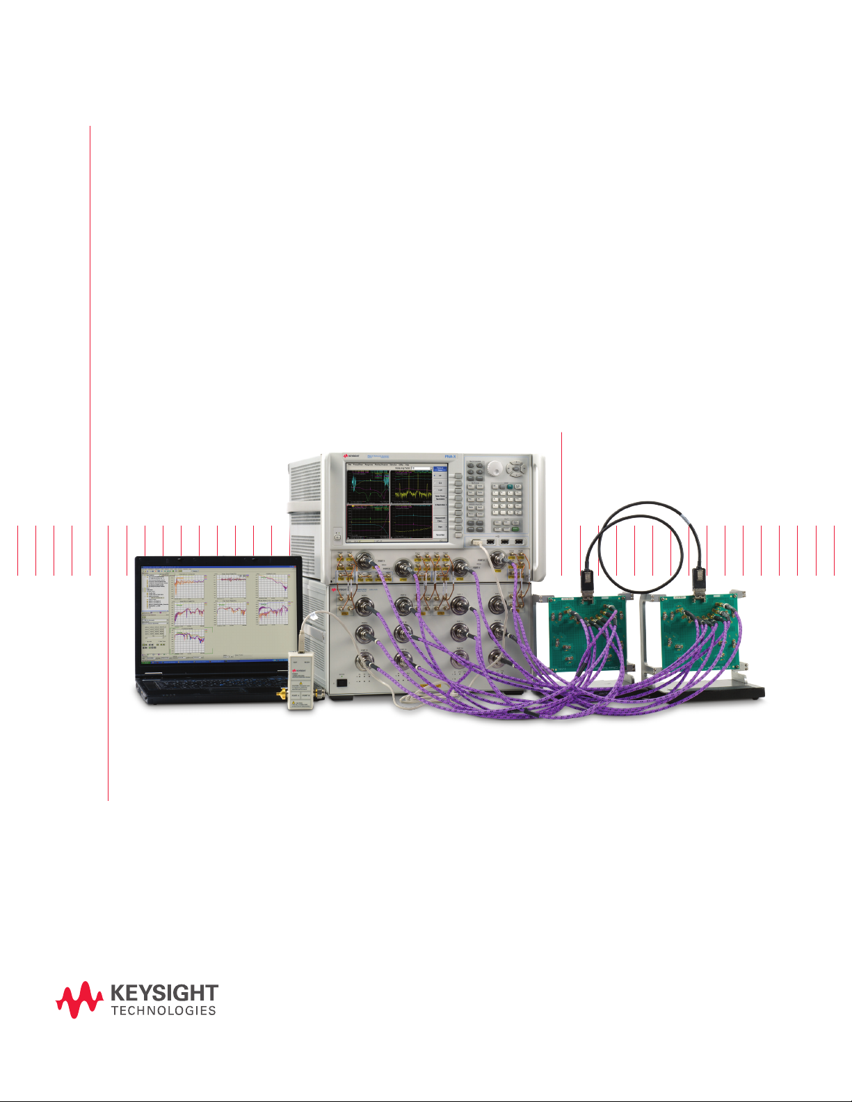
Physical Layer Test System
(PLTS) 2014
Technical Overview
Vector Network Analyzer-based and
Time Domain Reectometer-based Systems
Includes “What’s New in PLTS 2014 Software
Page 2
What’s New with PLTS 2014?
The new Physical Layer Test System (PLTS) 2014 includes
novel features that will help solve real world problems
for today’s signal integrity engineers. There are so many
signal integrity tools available for design, analysis, and
troubleshooting of high-speed interconnects it’s difficult
to manage them all. The Keysight Technologies, Inc. PLTS
design team has created version 2014, integrating new
features into PLTS for a substantial boost in productivity.
PLTS is the signal integrity industry solution for
measurement and analysis of physical layer devices.
Wizards help users to calibrate and measure multiport
devices with ease. Once measured, PLTS has a rich set of
displays, analysis, data reformatting and conversion tools,
as well as a versatile set of import and export capabilities.
PLTS works with PNA and ENA network analyzers, and
TDRs. Data and transmission line models can be exported
to, or imported from simulation tools. The analysis features
include single-ended and differential plots in frequency or
time, as well as eye diagrams and RCLG model extraction.
Major tool advancements
Many usability features have been incorporated into
PLTS 2014, but there are two new capabilities that are
considered breakthrough for the technical industry. The
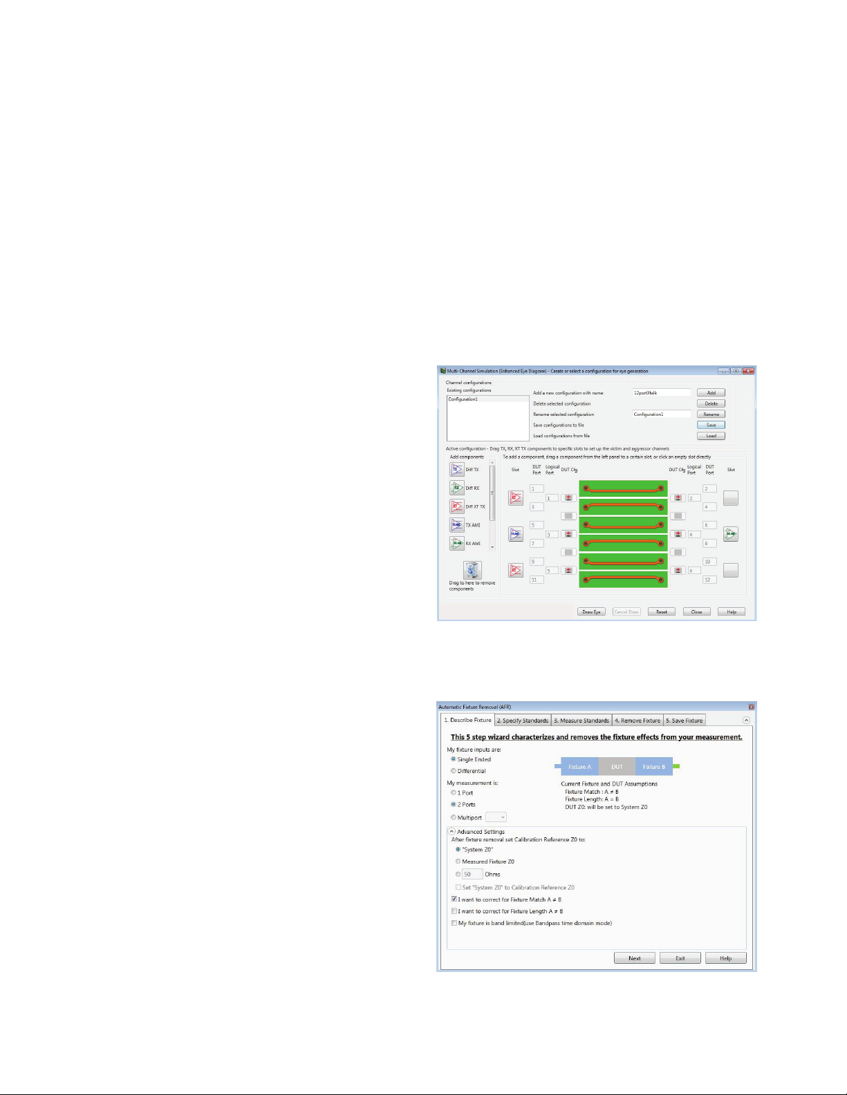
first is multi-channel simulation (Figure 1) and the other is
1-port automatic fixture removal (AFR)(Figure 2). Together
they create a time saving tool that helps the experienced
user accomplish more advanced analysis of the physical
layer channel.
The multi-channel simulation capability allows the user to
quickly measure a channel, remove any fixtures and then
simulate the measured channels’ performance. The newly
added capability to use vendor supplied IBIS-AMI models
for TX and RX creates real-world simulation results.
The 1-port automatic fixture removal tool is a breakthrough
extension of the 2X THRU AFR that saves the user from
designing and fabricating special calibration structures on
PCBs. Now, the test fixture itself can be used as the “1X
THRU” structure with an open circuit on port 2. This is
extremely helpful when working with FPGA applications
where it is nearly impossible to create a normal 2X THRU
structure. Furthermore, the accuracy can be enhanced by
using additional calibration structures together such as an
open, short and/or THRU. This error correction flexibility
gives the signal integrity engineer more control over
accuracy versus ease-of-use decisions that need to be
made for leading edge applications.
Figure 1. Multi-channel simulation capability allows users to quickly measure
a channel, remove any fixtures, and then simulate the measured channels’
performance using the newly added capability to use vendor supplied IBIS-AMI
models for TX and RX.
Built-in TX sources can be customized to match a
specified signal. Users can specify data rates, lengths
and voltages and then add noise, jitter, and pre-emphasis.
The built-in customizable RX allows the user to select
from the common CTLE, FFE, and DFE equalizers. Multiple
sources can be added to simulate aggressor cross talk for
multi-channel simulations. The resulting waveforms can be
displayed in multi-color eye diagrams with histograms for
common eye measurements.
Figure 2. 1-port AFR wizard provides more control of error correction techniques
by enabling the test fixture itself to be used as the calibration standard rather than
requiring the additional “2X THRU” structure to be fabricated.
2
Page 3
Why is Physical Layer Testing Required?
ISI Loss > 4 dB
Sample Compliance Interconnect
0 312.5 MHz 1.5625 GHz 3.125 GHz
–11.4
–15
SDD21 (dB)
0
The next generation computer and communication
systems now being developed will handle data rates of
multiple gigabits/second. Many systems will incorporate
processors and SERDES chip sets that exceed GigaHertz
clock frequencies. New and troubling input/output issues
are emerging as switches, routers, server blades, and
storage area networking equipment moving toward
10 Gbps data rates. Digital design engineers choosing
chip-to-chip and backplane technologies for these systems
are finding signal integrity challenges that have not been
encountered before.
Traditional parallel bus topologies are running out
of bandwidth. As parallel busses become wider, the
complexity and cost to route on PC boards increase
dramatically. The growing skew between data and clock
lines has become increasingly difficult to resolve within
parallel busses. The solution is fast serial channels. The
newer serial bus structure is quickly replacing the parallel
bus structure for high-speed digital systems. Engineers
have been turning to a multitude of gigabit serial
interconnect protocols with embedded clocking to achieve
the goal of simple routing and more bandwidth per pin.
However, these serial interconnects bring their own set of
problems.
In order to maintain the same total bandwidth as the
older parallel bus, the new serial bus needs to increase
its data rate. As the data rate increases through serial
interconnects, the rise time of the data transition from a
zero logic level to a one logic level becomes shorter. This
shorter rise time creates larger reflections at impedance
discontinuities and degrade the eye diagram at the end of
the channel. As a result, physical layer components such
as printed circuit board traces, connectors, cables, and IC
packages can no longer be ignored. In fact, in many cases,
the silicon is so fast that the physical layer device has
become the bottleneck.
In order to maintain signal integrity throughout the
complete channel, engineers are moving away from
single-ended circuits and now use differential circuits. The
differential circuit provides good Common Mode Rejection
Ratio (CMRR) and helps shield adjacent PCB traces from
crosstalk. Properly designed differential transmission lines
will minimize the undesirable effect of mode conversion
and enhance the maximum data rate throughput possible.
Unfortunately, differential signaling technology is not
always an intuitive science.
Differential transmission lines coupled with the microwave
effects of high-speed data have created the need for
new design and validation tools for the digital design
engineer. Understanding the fundamental properties
of signal propagation through measurement and postmeasurement analysis is mandatory for today’s leading
edge telecommunication and computer systems. The
traditional Time Domain Reflectometer (TDR) is still a very
useful tool, but many times the Vector Network Analyzer
(VNA) is needed for the complete characterization of
physical layer components. There is a strong need for
a test and measurement system that will allow simple
characterization of complex microwave behavior seen
in high speed digital interconnects. In fact, many digital
standards groups have now recognized the importance of
specifying frequency domain physical layer measurements
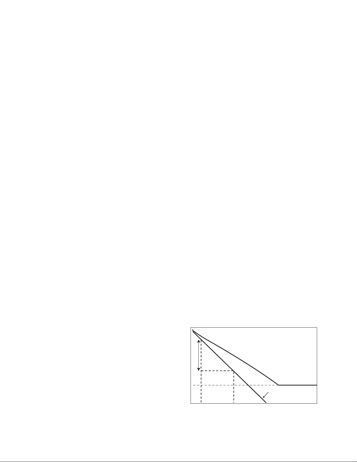
as a compliance requirement. Both Serial ATA and PCI
Express have adopted the SDD21 parameter (input
differential insertion loss) as a required measurement to
ensure channel compliance (Figure 3). This parameter
is an indication of the frequency response that the
differential signal sees as it propagates through the highspeed serial channel. An example of a proposed SDD21
compliance mask is shown in Figure 5 for the Channel
Electrical Interface (CEI) working group for the Optical
Internetworking Forum (OIF).
Figure 3. Today’s digital standards are now using frequency domain
measurements for compliance testing, such as this input differential insertion loss
(SDD21) mask for XAUI.
3
Page 4
Single ended
Port 1
Single ended
Port 2
Single ended
Port 3
Single ended
Port 4
Differential
Port 2
Differential
Port 1
Device under test
+
–
+
–
Why is Physical Layer Testing Required? (continued)
A single test system can provide the total
view
As the combination of both time-domain and frequency
domain analysis becomes more important, the need for
multiple test systems becomes difficult to manage. A
single test system that can fully characterize differential
high-speed digital devices, while leaving domain and
format of the analysis up to the designer, is a very
powerful tool. Keysight’s Physical Layer Test System
(PLTS) is designed specifically for this purpose.
PLTS has been designed specifically for signal integrity
analysis. PLTS software guides the user through hardware
setup and calibration, and controls the data acquisition. It
automatically applies patented transformation algorithms
to present the data in both frequency and time domains,
in both forward and reverse transmission and reflection
terms, and in all possible modes of operation (singleended, differential, and mode-conversion).
A powerful virtual bit pattern generator feature allows
a user-defined binary sequence to be applied to the
measured data to convolve eye pattern diagrams. Next,
highly accurate RLCG 1 models can be extracted and used
to enhance the accuracy of your models and simulations.
PLTS provides design condence through
complete characterization
Physical-layer structures have increasingly become the
bottleneck in high-speed digital system performance. At low
data rates, these interconnects are electrically short. The
driver and receiver are typically the biggest contributors to
signal integrity. But as clock speeds, bus speeds, and link
speeds all push past the gigabit-per-second mark, physical
layer characterization becomes more critical.
Another challenge for today's digital designers is the trend to
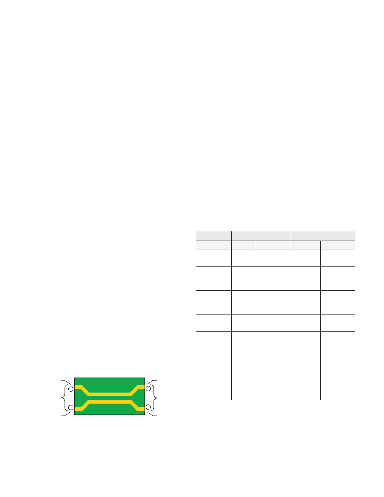
differential topologies. Fully understanding device performance
requires analysis in all possible modes of operation.
Time-domain analysis is typically used for characterization
of these physical-layer structures, but often, the designer
concentrates only on the intended modes of operation. For
a complete time-domain view, step and impulse responses
in reflection and transmission (TDR and TDT) must be
seen. The analysis must include the unintended modes of
operation as well.
Frequency-domain analysis, again in all possible modes
of operation, is also necessary for fully characterizing
these physical-layer structures. The s-parameter model
describes the analog behavior exhibited by these digital
structures. This behavior includes reflections from
discontinuities, frequency dependent losses, crosstalk, and
EMI performance.
For translating device performance into standards
compliance, eye diagrams add an important statistical
analysis. And for leveraging this complete characterization
into improved simulations, measurement-based
s-parameter or RLCG model extraction completes the
picture.
Time domain Frequency domain
Mode TDR TDT Reection Transmission
Differential TDD11
TDD22
Diff-to-comm
SCD12
Comm-to-diff
SDC12
Common TC C11
Single-ended
Figure 5. Complete characterization includes forward and reverse transmission and
reflection, in all possible modes of operation, in both frequency and time domains.
TC D11 TCD21
TDC 11 TDC21
TCC22
T11 T21 T31 T41 S11 S21 S31 S41
T22 T12 T32 T42 S22 S12 S32
T33 T13 T23 T43 S33 S13 S23
T44 T14 T24 T34 S44 S14 S24
TDD21
TDD12
TCD22
TDC22
TCC21
TCC12
SDD11
SDD22
SC D11
TCD12
SD C11
TD C12
SC C 11
SCC22
SDD21
SDD12
SCD21
SCD22
SDC21
SDC22
SCC21
SCC12
S42
S43
S34
Figure 4. A differential structure operates in many modes. Single-ended analysis
can reveal sources of asymmetry on this differential transmission line.
4
1. An RLCG equivalent circuit model, also known as Telegrapher’s Parameters, describes the electrical behavior of a passive transmission line. The
model is a distributed network consisting of series resistance and inductance (R and L) and parallel capacitance and conductance (C and G).
Page 5
Why is Physical Layer Testing Required? (continued)
Passive differential structure
Differential
stimulus
Differential
response
Common-mode response
(unintended mode conversion)
PLTS enables mode-conversion analysis for
early insight into EMI problems
The benefits of differential signaling include lower voltage
swings, immunity from power supply noise, a reduced
dependency on RF ground, and improved EMI performance
(reduced generation and susceptibility). The extent to
which a device can take advantage of these benefits is
directly related to device symmetry.
Symmetric devices only respond to, and only generate,
differential signals. These ideal devices do not respond
to or generate common-mode signals, and they reject
radiated external signals (i.e., power supply noise,
harmonics of digital clocks or data, and EMI from other RF
circuitry).
Asymmetric devices however, do not exhibit these
benefits. When stimulated differentially, an asymmetric
device will produce a common-mode response in addition
to the intended differential response, and cause EMI
radiation. Conversely, with a common-mode stimulus, an
asymmetric device will produce an unintended differential
response. This mode conversion is a source of EMI
susceptibility.
Mode-conversion analysis is an important tool for
understanding and improving device symmetry, and
provides the designer with early insight to identify and
resolve EMI problems at the design stage (Figure 6).
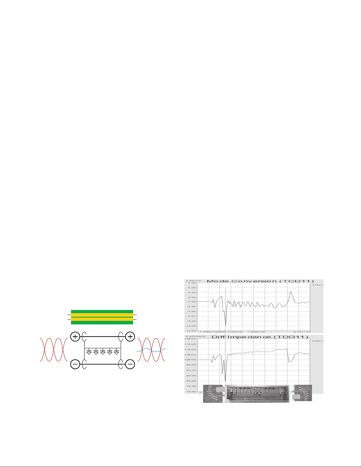
Mode conversion
A practical application of how mode conversion helps
identify problems in physical layer devices is shown in
Figure 7. This shows a XAUI backplane with two daughter
cards that typically transmit data at 3.125 Gbps. The
design objective for this high-speed differential channel
is to minimize the crosstalk between adjacent differential
PCB traces throughout the length of the channel. The
channel consists of the linear passive combination of the
backplane and two daughter cards. Any mode conversion
from differential mode to common mode will generate
EMI and create crosstalk that will be incident upon other
channels and will degrade performance. However, locating
the exact structure within the channel that creates the
most mode conversion is not simple.
Looking at Figure 7, the differential to common mode
conversion time domain reflection parameter (TCD11)
is time aligned with the differential impedance profile
of the channel (TDD11) below it. A marker is placed on
the largest magnitude peak of TCD11. This is where the
physical structure within the channel is creating the
most mode conversion and thus the source of the most
crosstalk. We can align the TDD11 to the TCD11 in time
and therefore co-locate the problematic structure on
TDD11. To relate this structure to the channel, we use
the differential impedance profile as a reference. From
previous analysis, we know that the two capacitive
discontinuities on TDD11 are the daughter card via
field and motherboard via field, respectively. Since the
Figure 6. Asymmetric devices cause mode-conversions, which are indicators of
EMI generation and susceptibility.
Figure 7. By aligning the impedance profile with the mode conversion profile,
PLTS allows the pinpointing of crosstalk-generating structures within physical layer
devices.
5
Page 6
Why is Physical Layer Testing Required? (continued)
marker falls upon the second discontinuity on TDD11, it
is deduced that the motherboard via field is the biggest
culprit to causing crosstalk in adjacent channels. The
motherboard via field was subsequently rerouted and
the crosstalk generation was reduced considerably. This
shows how identifying the mode conversion in a channel
can be intuitive with proper analysis.
Dynamic range
High-dynamic range is important for a number of reasons.
Certainly, measurements of very low levels of crosstalk are
possible, but this is only one parameter where dynamic
range is important.
More important is the ability to overcome masking effects
of multiple discontinuities, which in systems with lower
dynamic range would attenuate the stimulus such that
deep structures would become invisible.
And most importantly for differential devices, highdynamic range allows for identification of very low levels
of mode-conversion, which are the direct result of device
asymmetry. This allows early resolution of potential EMI
issues.
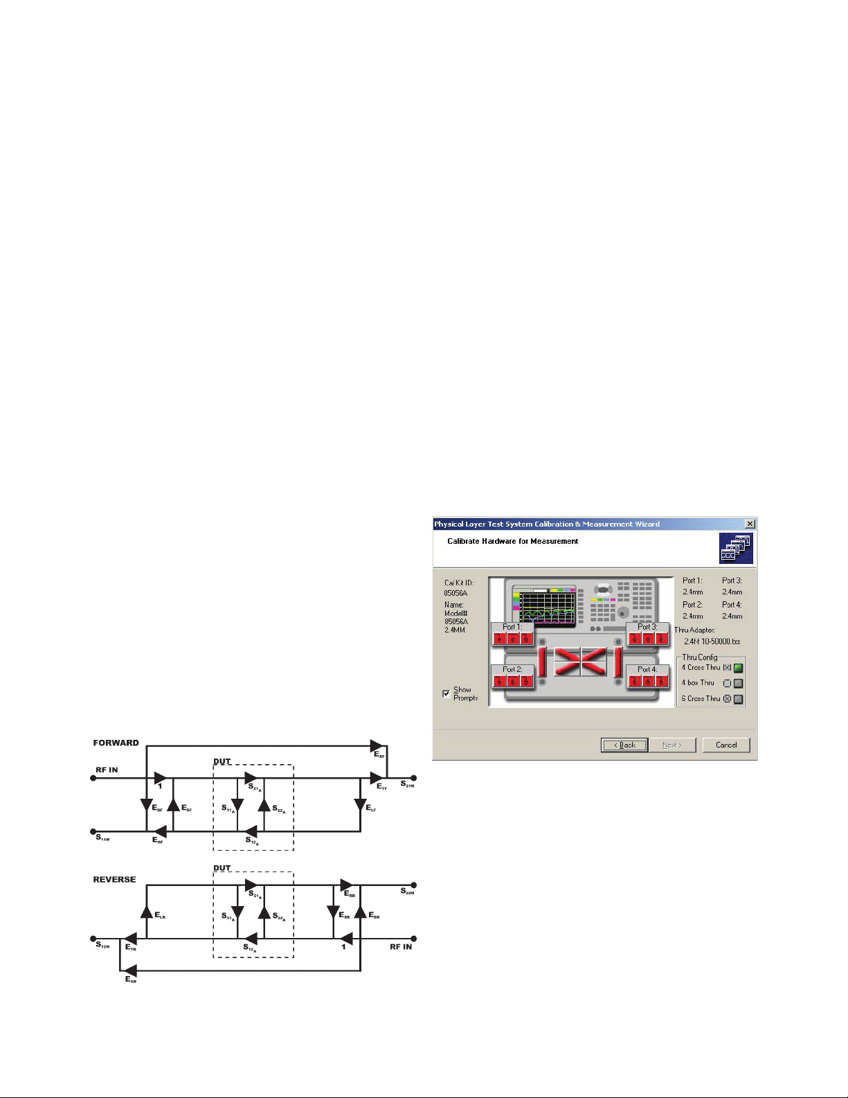
data is used to calculate a 72-term error model, which is
then used to remove the effects of systematic errors from
subsequent measurements.
Utilizing three impedance standards (the short, open, and
load) and a thru standard, the error model compensates
for directivity, source match, load match, reflection and
transmission tracking (frequency response), and crosstalk
in both forward and reverse directions.
Four-port TRL (Thru-Reect-Line)
TRL calibration is primarily (but not exclusively) used in
non-coaxial environments, such as in-fixture or microprobe
measurements. It determines the same error model as
the SOLT calibration, although it uses different calibration
standards - a thru, a reflection standard (a short), and one
or more offset length transmission lines.
TRL calibration typically provides more accuracy than
SOLT and is only available for PNA-based systems (it is
not supported for 872x-based systems)(Figure 9).
Accuracy through error-correction
VNA-based systems
Four-port SOLT (Short-Open-Load-Thru)
The most common technique for both coaxial and noncoaxial environments, SOLT calibration, is a vector error
correction process (Figure 8) that characterizes systematic
error by measuring known calibration standards. This
Figure 9. The PNA network analyzer-based calibration interface simplifies a complex
process, allowing full error-correction in minutes, not hours.
Figure 8. The vector-correction process characterizes systematic error to provide
superior accuracy in network analyzer-based systems.
6
Page 7
Why is Physical Layer Testing Required? (continued)
Four-port LRM (Line-Reect-Match)
LRM is a variation of TRL, and determines the same
error model as the SOLT and TRL calibrations, although
it uses different (and fewer) calibration standards – a
transmission line, a reflection standard (a short), and a
load.
In broadband non-coaxial environments, specifically
microprobing, LRM can offer an accuracy improvement
over TRL due to bandwidth limitations of the TRL line
standards.
LRM calibration is only available for PNA network
analyzer-based systems (it is not supported for Keysight
872x-network analyzer based systems).
Four-port Electronic Calibration (ECal)
Reference plane calibration (RPC)
RPC adjusts the calibration reference plane to the end of
the test cables and automatically performs the de-skew
operation (see above).
This calibration is available for all supported TDR-based
systems.
Normalization
Normalization is an error correction process that
characterizes systematic error by measuring known
calibration standards (a short, a load, and a thru) to
calculate an error model, which is then used to remove
the effects of systematic errors from subsequent
measurements.
For electronic calibration to 9 GHz, the Keysight N4430B
ECal Module (30 kHz to 9 GHz) is supported by all of the
PLTS VNA-based systems. With one set of connections,
this solid-state tuner simulates all of the impedance states
required for full four-port error correction with accuracy
that is generally better than SOLT, but somewhat less than
TRL.
TDR-based systems
Module calibration
Module calibration, also called vertical calibration,
calibrates the gains, offsets, and timing for each channel.
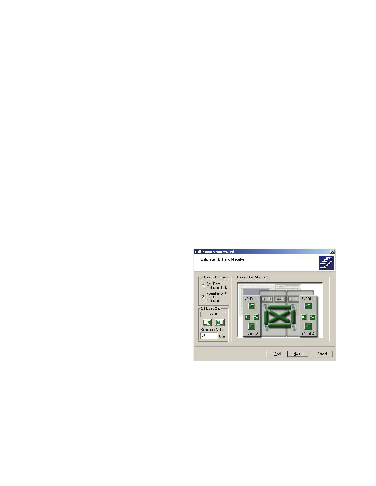
At the start of the TDR calibration process (Figure 10),
PLTS will report that a module calibration is valid,
recommended, or required.
This calibration is available for all supported TDR-based
systems.
De-skew
Asymmetry in a differential system – between the two
step generators, between the two receivers, etc… – can
potentially lead to imbalances or errors in resulting
measurements.
The error model compensates for directivity, source match,
and reflection tracking (frequency response). This is the
most accurate calibration type for TDR.
Note: Normalization is available for the Keysight 86100
family of oscilloscopes only.
Figure 10. Like the PNA network analyzer-based calibration interface, the TDRbased calibration interface guides the user through the calibration(s) reducing
operator error and saving time.
When differential measurements are selected in the
calibration process, PLTS automatically performs this
operation to remove length variance from cables or test
fixtures.
This calibration is available for all supported TDR-based
systems.
7
Page 8
Why is Physical Layer Testing Required? (continued)
Remove unwanted effects from the
measurement
Error correction
Over the years, many different approaches have been
developed for removing the effects of the test fixture
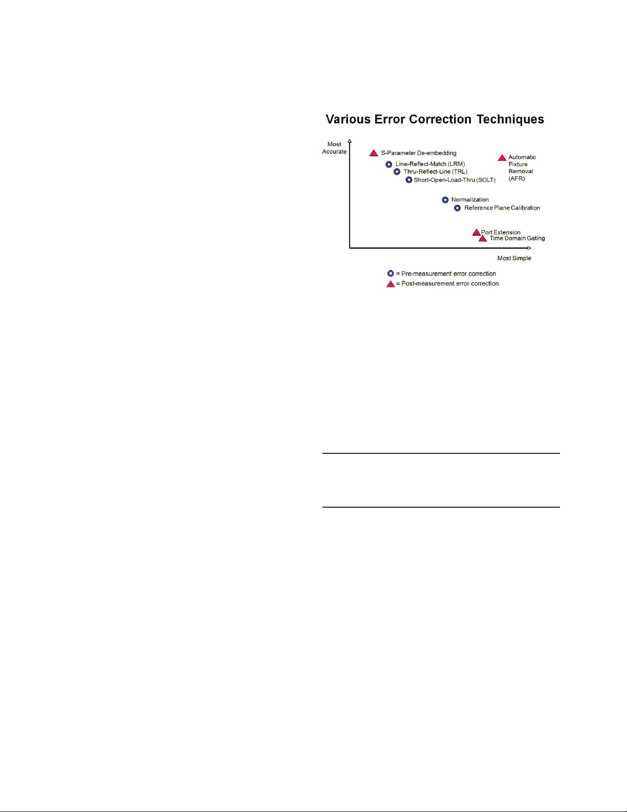
from the measurement (shown in Figure 11). The level of
difficulty for each error correction technique is linearly
related to the accuracy of each method. Time domain
gating is perhaps the simplest and most straightforward
method, but it is also the least accurate. Likewise,
de-embeding is the most complicated method, but it is
the most accurate. It is important to have a test system
that will allow flexibility of choosing the method of error
correction desired for each application.
Error correction techniques fall into two fundamental
categories: direct measurement (pre-measurement
processing) and de-embedding (post-measurement
processing). Direct measurement requires specialized
calibration standards that are connected to the end of
a coaxial test cable and measured. The accuracy of the
device measurement relies on the quality of these physical
standards. De-embedding uses a model of the test fixture
and mathematically removes the fixture characteristics
from the overall measurement. This fixture de-embedding
procedure can produce very accurate results.
Figure 11. PLTS has advanced error correction techniques to allow flexibility
for many applications.
Port Extension (also known as Phase Rotation)
mathematically extends the calibration reference plane to
the DUT.
This technique is easy to use, but assumes the fixture –
the unwanted structure – looks like a perfect transmission
line: a flat magnitude response, a linear phase response,
and constant impedance. If the fixture is very well
designed, this technique can provide good results.
Because gating essentially considers the magnitude
of the unwanted discontinuity, and Port Extensions
consider phase (electrical length), using the two
tools together may provide optimum results.
8
Page 9
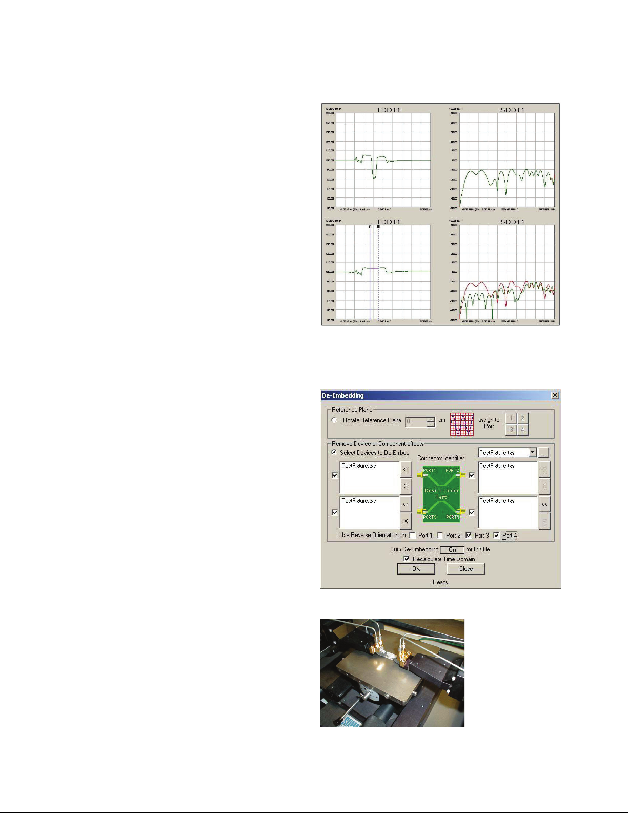
Time-domain gating (Figure 12) is similar to port
extension, in that it is also very easy and fast. The user
simply defines two points in time or distance, and the
software mathematically replaces the actual measured
data in that section with data representing an "ideal"
transmission line. The return loss is then recalculated to
show the effects of the change in the frequency domain.
One practical application of time-domain gating is as a
confidence check before replacing a suspect connector.
Figure 14 illustrates how this technique might be used.
De-embedding (Figure 13) uses an accurate linear
model of the fixture, or measured s-parameter data
of the fixture. This fixture data can then be removed
mathematically from the DUT measurement data in postprocessing.
Calibration at the DUT reference plane has the advantage
that the precise characteristics of the fixture do not
need to be known beforehand, as they are measured and
corrected for during the calibration process.
An example of this technique is microprobing using a
calibration substrate, where the calibration reference
plane is established at the probe tips, rather than at the
end of the coaxial test cables.
Advanced calibration techniques (TRL/LRM) – originally
developed for wafer probing applications – provide
additional options.
Figure 12. In this rather extreme example of time-domain gating, the top plots show the
measured differential step impedance and return loss. The lower left plot shows a gate
added to remove the large discontinuity in the center of the trace. On the lower right,
the measured and the recalculated return losses are displayed. In this case, the gate
improved the return loss by more than 10 dB within the frequency band of interest.
Figure 13. The effects of test fixtures can be removed from the device in postprocessing through de-embedding.
Figure 14. A microprobing application, where the calibration is performed using an
impedance standard substrate, establishes the calibration reference plane at the
probe tips.
9
Page 10
PLTS Support for Microprobing Applications
Keysight works closely with leading microprobe and probe
station suppliers to provide the best complete system
solutions possible.
One of the most significant measurement challenges is
connectivity. Test equipment provides a controlled coaxial
environment, but what if the DUT – the backplane, the
interface connector, the IC package – is non-coaxial?
Test fixtures can provide the required connectivity, but
at a cost. The quality of the test fixture – its connectors,
impedance discontinuities, parasitics, and dielectric
losses – all contribute to less than ideal performance
of the fixture. Subsequently, the accuracy of the device
measurement is degraded.
Several techniques are available to remove these
fixture effects (see Remove Unwanted Effects from the
Measurement on page 7), but the accuracy of these
techniques is greatly impacted by the quality of the fixture
itself, or the availability of an accurate s-parameter model
of the fixture (used for de-embedding).Microprobing can
offer the user the ability to forego the test fixture and
launch the stimulus directly at the device input. The
response can be measured directly at the device output.
Additionally, when calibration substrates are available,
calibration can be performed directly at the probe tips. This
achieves co-location of the calibration reference plane with
the device measurement reference plane.
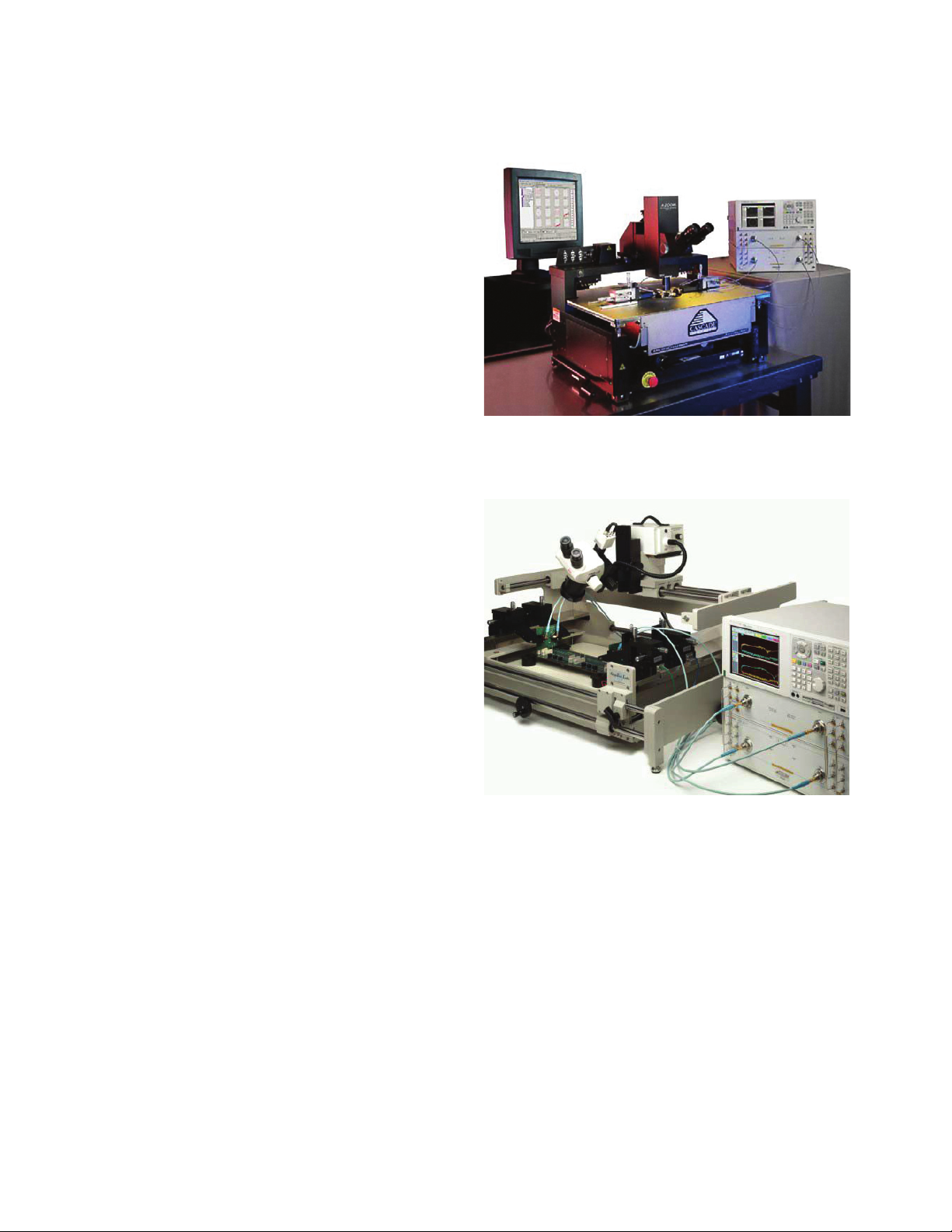
Figure 15. Cascade Microtech’s Summit probe station.
PLTS has the flexibility to accommodate many microprobe
configurations. By adding the calibration substrate
coefficients as a calibration kit, the process becomes as
straightforward as a coaxial calibration.
Figure 16. GigaTest Lab’s GTL-4060 probe station.
10
Page 11
Step 1
System setup
Step 2
Calibration
Step 3
Device
measurement
TDR
setup
process
VNA
setup
process
Setup and
calibration
complete
TDR
setup
Select calibration
and measurement
parameters
VNA
setup
TDR
calibration
VNA
calibration
PLTS Simplies the Measurement Process
Device characterization with PLTS software is
straightforward. The user interface has been designed to
make setup, calibration, and measurement intuitive and
error-free. A wizard guides the user through all of the
required steps. The last prompt is to connect the deviceunder-test and initiate the measurement. Setup and
calibration differs slightly between TDR-based and VNAbased systems. However, in both cases the PLTS software
provides an intuitive wizard to assist in the step-by-step
process.
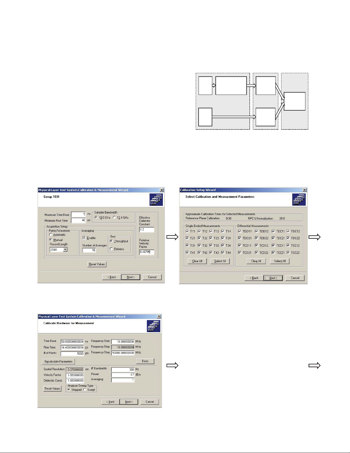
Easy setup
Step 1.
In the first step, PLTS software automatically polls the GPIB,
and prompts the user to accept or modify the default parameters
based on hardware capabilities.
TDR setup
Figure 18. PLTS software completely controls the hardware setup
via GPIB.
Figure 17. PLTS has a three-step system set up to make measurements intuitive
and error-free.
Figure 19. The user may calibrate only for the specific parameters of
interest. Estimated calibration times are calculated based on selections.
VNA setup
Figure 20. Default parameters are calculated from system capabilities.
User modifications are interactive.
Parameter selection not required in the VNA setup
11
Page 12
PLTS Simplies the Measurement Process (continued)
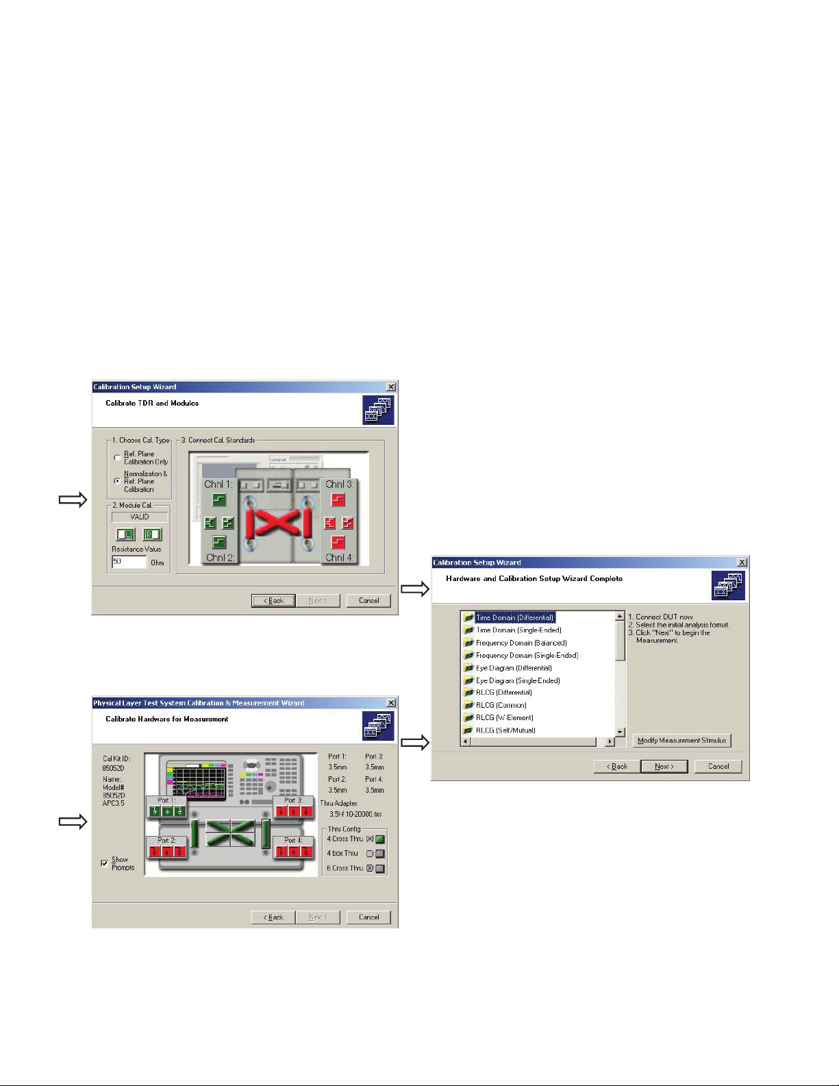
Step 2. Calibration
After the system setup, the calibration method is
selected. Again, the wizard simplifies the process and
provides the greatest flexibility to the user.
The calibration interface shows the required calibration
standards as icons, which are initially represented in
red. As the user connects the standards, and mouseclicks the corresponding icon, the system makes the
measurement, and the icon color changes to green
(indicating completion). When all of the icons are green,
the calibration is complete.
TDR calibration
Step 3. Device measurement
For both TDR and VNA systems, when the calibration is
completed, PLTS prompts the user to connect the deviceunder-test, and select an initial analysis format.
Then, the system makes all of the measurements required
for the complete characterization.
With one setup, calibration and measurement, up to
sixty-four time-domain and frequency-domain device
parameters are available
Figure 21. The TDR system calibration wizard provides status and controls module and
reference plane calibrations, de-skew, and normalization.
VNA calibration
Figure 22. The VNA system calibration wizard simplifies four-port SOLT, TRL, and
LRM error correction.
Setup and calibration complete
Figure 23. All domains and formats are available immediately after the measurement is completed.
12
Page 13
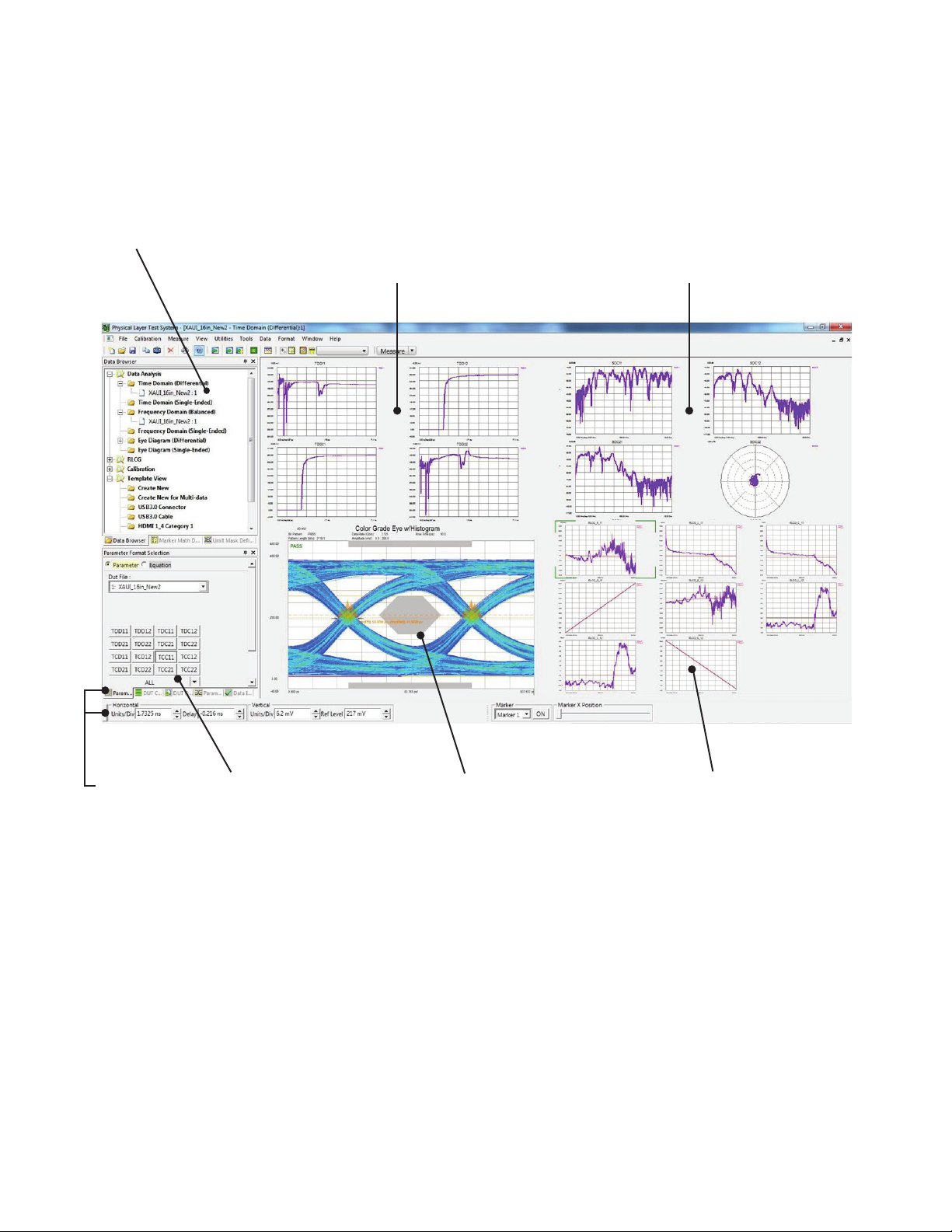
PLTS Simplies the Measurement Process (continued)
Data analysis with n-port PLTS
File and view management
with the data browser
Time domain analysis:
2
– 2 n
parameters
– 7 formats
– time or distance
Frequency domain analysis:
2
– 2 n
parameters
– 8 formats
Format, scaling,
and marker control
with easy access
toolbars
Plot and trace
management with
context-sensitive
parameter buttons
Eye diagram analysis:
2
– n
parameters
– 8 formats
13
RLCG model extraction
2
– 2 n
parameters
Page 14
PLTS Simplies the Measurement Process (continued)
4-port data analysis
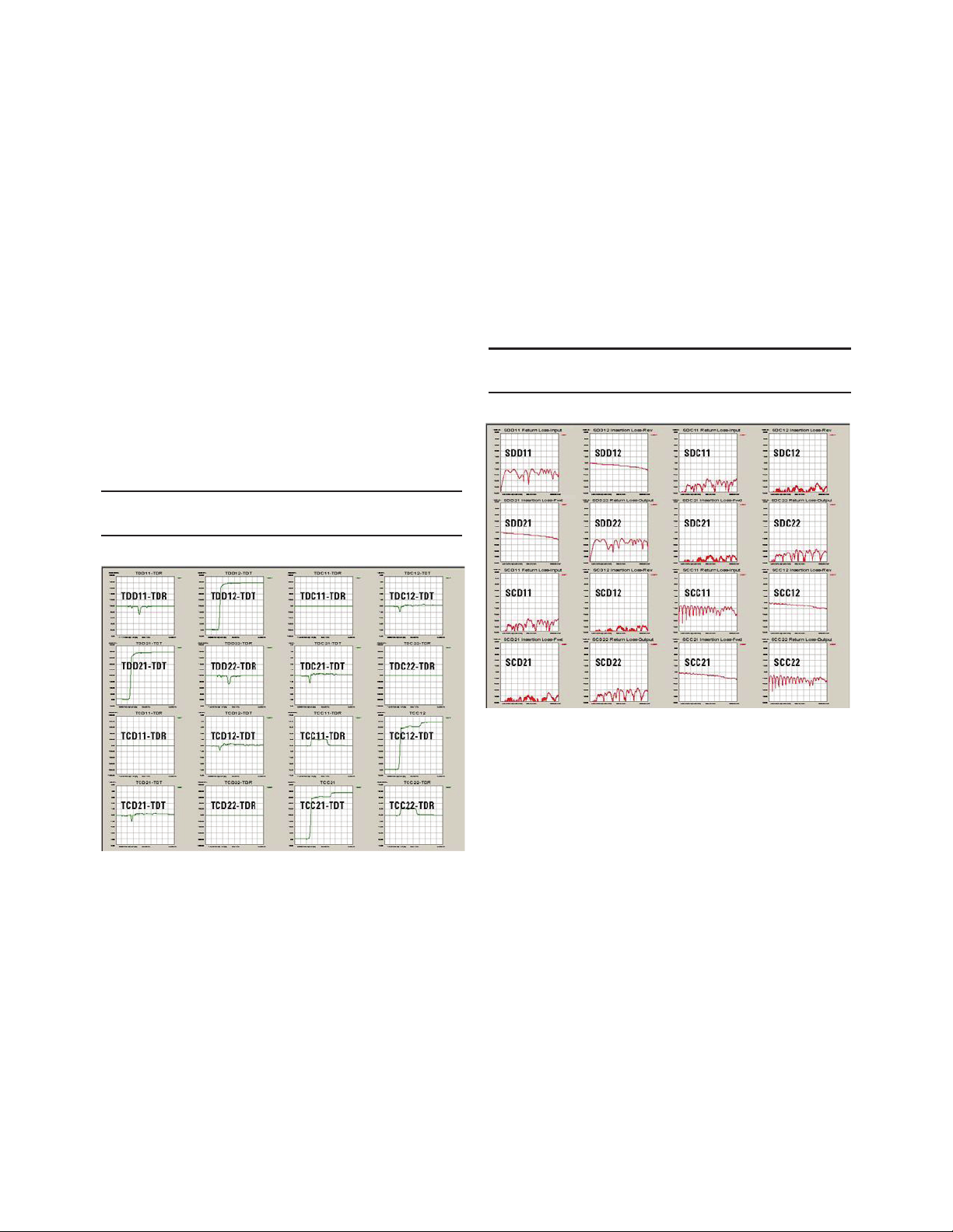
All supported analysis types and formats are available
immediately after the measurement is completed, and at
any time there after. PLTS flexibility allows the user to
begin where they are most familiar.
Time-domain analysis
The mixed-mode time domain is a common starting point.
Initially, sixteen parameters are displayed in thumbnail
view as shown below. These thumbnails represent four
modes of device operation: differential, common-mode,
and the two mode-conversion types (common-mode
stimulus with differential response and differential
stimulus with common-mode response). A double mouseclick on any of these thumbnails will expand the selected
parameter to full screen for closer analysis.
Not shown here are the additional sixteen single-ended
time-domain parameters.
Frequency-domain analysis
The mixed-mode frequency domain is another common starting point.
Initially, sixteen parameters are displayed in thumbnail view as
shown below. These thumbnails represent four modes of device
operation: differential, common-mode, and the two mode-conversion types (common-mode stimulus with differential response
and differential stimulus with common-mode response). A double
mouse-click on any of these thumbnails will expand the selected
parameter to full screen for closer analysis.
Not shown here are the additional sixteen single-ended
frequency-domain parameters.
Figure 24. The mixed-mode time-domain matrix.
Figure 25. The mixed-mode frequency-domain matrix.
14
Page 15
Self Resistance Self Inductance
Self Capacitance
Self Conductance Mutual
Resistance
Mutual
Inductance
Mutual
Capacitance
Mutual
Conductance
PLTS Simplies the Measurement Process (continued)
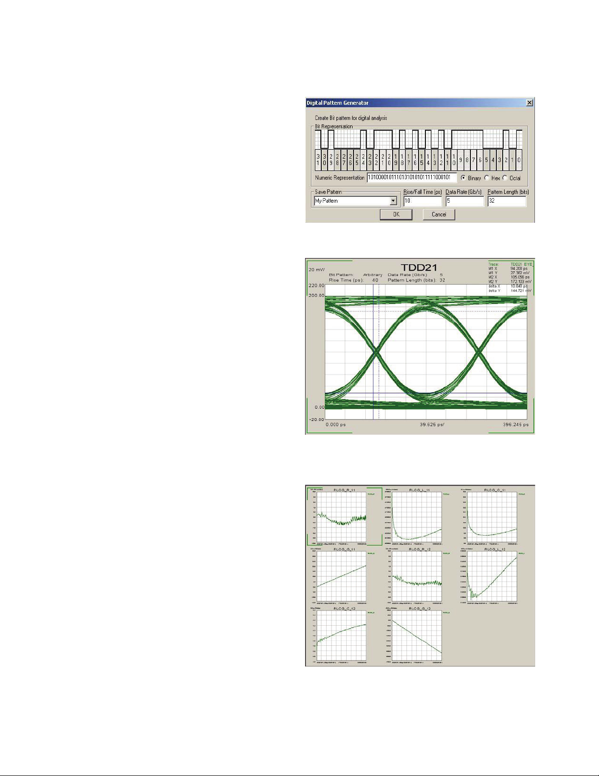
Measurement-based eye diagram analysis
Using the built-in digital pattern generator, the user is
able to define virtual bit pattern (as wide as 232-1 bits).
PLTS then convolves the selected bit pattern with the
device impulse response to create an extremely accurate
measurement-based eye pattern diagram.
This eliminates the need for a hardware pulse/pattern
generator, and its flexibility allows for a great deal of
"What if…" analysis.
Figure 26. The digital pattern generator.
After the eye pattern is generated, marker functions can
be used to make typical measurements like jitter, eye
opening, rise and fall times, and more.
RLCG model extraction
RLCG (resistance, inductance, capacitance, and
conductance) models describe the electrical behavior of
passive transmission lines in an equivalent circuit model.
From the measured S-parameters of a device, PLTS
calculates the R, L, C, G, complex propagation constant,
and complex characteristic impedance.
This provides a highly accurate, measurement-based
coupled transmission line model for export into modeling
and simulation software such as Keysight ADS, Synopsis
HSPICE, and others.
Figure 27. Eye pattern diagram.
Figure 28. RLCG model extraction (W-Element shown).
15
Page 16
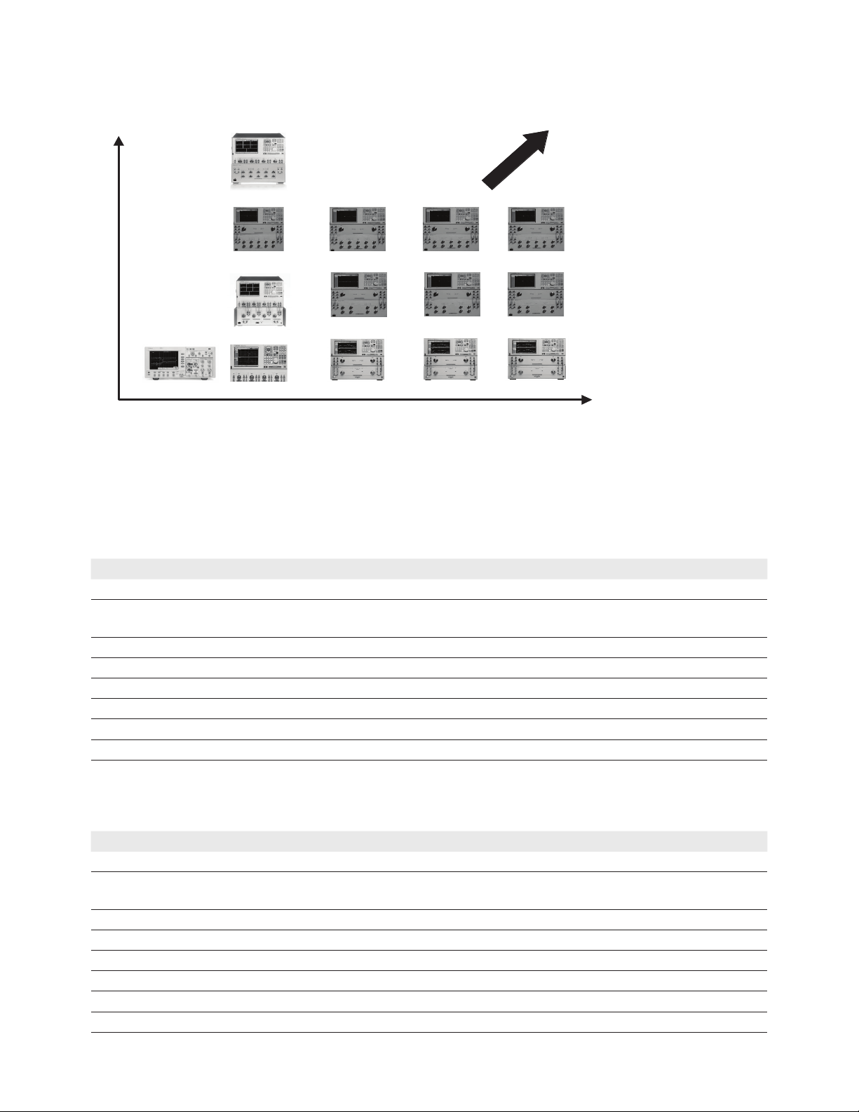
Frequency
Number of channels
4-port 50 GHz
4-port 67 GHz
4-port 18 GHz
12-port 20 GHz
12-port 50 GHz
12-port 67 GHz
4-port 20 GHz
14-port 20 GHz
N-port
8-port 20 GHz
8-port 50 GHz
4-port 40 GHz
12-port 40 GHz
8-port 40 GHz
8-port 67 GHz
PLTS Signal Integrity Solutions Portfolio
PNA-Based Examples
Below are 4-port PLTS configuration examples. For a complete list of compatible test sets go to
www.keysight.com/find/multiport. For a custom test set solution contact your local Keysight sales representative.
PLTS multiport conguration (4-port 67 GHz system)
Qty Default options Available options Description
Physical layer test system, 11 ps, 67 GHz
1 N5227A-401 10 MHz to 67 GHz vector network analyzer, 4-ports, congurable
test set
4 N4 421B-K67 Test port cables, 3 ft., 1.85 mm (m-f)
1 N1930B-1FP PLTS base analysis networked license
1 N1930B-3FP PLTS measurement and cal networked license
1 N1930B-5FP PLTS advanced calibration (AFR) xed license
1 PS-S20-01 N4694A Recommended Startup Assistance
1 Option 00F 1.85 mm ECal kit
PLTS multiport conguration (4-port 50 GHz system)
Qty Default options Available options Description
1 N5225A-401 10 MHz to 50 GHz vector network analyzer, 4-ports, congurable
4 N4421AK20 Test port cables, 3 ft., 2.4 mm (m-f)
1 N1930B-1FP PLTS base analysis xed license
1 N1930B-3FP PLTS measurement and cal xed license
1 N1930B-5FP PLTS advanced calibration (AFR) xed license
1 PS-S20-01 Recommended Startup Assistance
1 N4693A-00F 2.4 mm ECal kit
Physical layer test system, 15 ps, 50 GHz
test set
16
Page 17

PLTS Signal Integrity Solutions Portfolio (continued)
PLTS multiport conguration (4-port 43.5 GHz system)
Qty Default options Available options Description
Physical layer test system, 16.5 ps, 43.5 GHz
1 N5224A-401 10 MHz to 43.5 GHz vector network analyzer, 4-ports, congurable
test set
4 N4421AK20 Test port cables, 3 ft., 2.4 mm (m-f)
1 N1930B-1FP PLTS base analysis xed license
1 N1930B-3FP PLTS measurement and cal xed license
1 N1930B-5FP PLTS advanced calibration (AFR) xed license
1 PS-S20-01 Recommended Startup Assistance
1 N4693A-00F 2.4 mm ECal kit
PLTS multiport conguration (4-port 26.5 GHz system)
Qty Default options Available options Description
Physical layer test system, 27 ps, 26.5 GHz
1 N5222A-401 10 MHz to 26.5 GHz vector network analyzer, 4-ports, congurable
test set
4 N4419AK 20 Test port cables, 3 ft., 3.5 mm (m-f)
1 N1930B-1FP PLTS base analysis xed license
1 N1930B-3FP PLTS measurement and cal xed license
1 N1930B-5FP PLTS advanced calibration (AFR) xed license
1 PS-S20-01 Recommended Startup Assistance
1 N443 3A-010 3.5 mm ECal kit
PLTS multiport conguration (4-port 20 GHz system)
Qty Default options Available options Description
Physical layer test system, 35 ps, 20 GHz
1 N5230C-245 4-por t PNA-L network analyzer
4 N4 419AK20 Test port cables, 3 ft., 3.5 mm (m-f)
1 N1930B-1FP PLTS base analysis xed license
1 N1930B-3FP PLTS measurement and cal xed license
1 N1930B-5FP PLTS advanced calibration (AFR) xed license
1 PS-S20-01 Recommended Startup Assistance
1 N4433A-010 3.5 mm ECal kit
17
Page 18

PLTS multiport conguration (16-port 26.5 GHz system)
Qty Default options Available options Description
Physical layer test system, 27 ps 26.5 GHz
1 N5222A-401 10 MHz to 26.5 GHz vector network analyzer, 4-port congurable
test set
1 N5222A-551 N-port calibrated measurements
16 N4 419AK20 Test port cables, 3 ft., 3.5 mm (m-f)
1 U3042AE12 12-port 26.5 GHz multiport test set
1 N1930B-1FP PLTS base analysis xed license
1 N1930B-3FP PLTS measurement and cal xed license
1 N1930B-5FP PLTS advanced calibration (AFR) xed license
1 N1930B-7FP PLTS N-port measurement and analysis xed license
1 PS-S20-01 Recommended Startup Assistance
1 N4433A-010 3.5 mm Ecal kit
PLTS multiport conguration (12-port 50 GHz system)
Qty Default options Available options Description
Physical layer test system, 15 ps 50 GHz
1 N5225A-401 10 MHz to 50 GHz vector network analyzer, 4-port congurable test
set
1 N4 421A-1CP Rack-mount kit with handles
12 N4421AK 20 Test port cables, 3 ft., 2.4 mm (m-f)
1 U3045AE08 8-port 50 GHz S-parameter multiport test set
1 N1930B-1FP PLTS base analysis xed license
1 N1930B-3FP PLTS measurement and cal xed license
1 N1930B-5FP PLTS advanced calibration (AFR) xed license
1 N1930B-7FP PLTS N-port measurement and analysis xed license
1 PS-S20-01 Recommended Startup Assistance
1 N4694A Option 00F 2.4 mm Ecal kit
18
Page 19

PLTS Ordering Guide
PLTS system requirements
To ensure that PLTS operates effectively, your PC should have the following minimum requirements:
Measurement mode ONLY Off-line analysis mode
CPU 1 GHz 1.5 GHz
Main memory (RAM)
Virtual memory - As a general
rule, virtual memory should be
1.5 to 2 times the size of main
memory.
GPIB interface
With PLTS 4.2, PLTS can connect
to a PNA over LAN
Operating systems Windows XP, Vista 32, Vista 64, and Windows 7. Windows XP, Vista 32, Vista 64, and Windows 7.
Screen resolution 1280 x 1024 or greater required 1280 x 1024 or greater required
Display colors High Color (16 Bit) or greater High Color (16 Bit) or greater
In the lab, controlling test
equipment and making quick analysis
of the results.
512 MB - 1 GB is recommended when
measuring 16,000 points with the PNA B-model
network analyzers.
2.5 GB+ 2.5 GB+
Keysight 82357A USB/GPIB Inter face for
Windows or supported GPIB card (any National
Instruments or Keysight 82340/41 or 82350
GPIB card)
In your ofce, per forming “What if...” analysis,
characterization, cross-domain analysis, ltering,
waveform math, and eye diagram simulation.
1 GB
No GPIB connection is required to use PLTS
off-line.
Saved (stored) measurement les can be recalled
at any time for analysis.
Upgrades from 2-port PNA to 4-port PLTS
Supported network analyzers
PNA model
number
E8364A/B/C
E8364A/B/C 10 MHz to 50 GHz
E8363A/B/C
E8363A/B/C 10 MHz to 40 GHz
Required Compatible Not tested or
Network analyzer options
014 010, UNL
specied
016, 080,
081, 083
H08, H11
Required test
set
N4 421B
N4420B
System frequency
range
45 MHz to 50 GHz
45 MHz to 40 GHz
Required
application
software
N1930B
19
Page 20

PLTS Ordering Guide (continued)
PNA support
2
The following are requirements for PNA Firmware. Firmware selection may depend upon the CPU.
http://na.support.keysight.com/pna/cputype.html (Internet connection required.)
– All PNA (E836xC) Series and PNA-L N5230C - A.09.33.09
– All PNA-X (N524x A) Series - A09.33.09
– All PNA (N522xA) Series - A09.33.09
– All models with 1.1 GHz CPU: (E8361A, E8362B, E8363B, E8364B, N5230A) - A.07.50.48
– Any model using XP on 500 MHz CPU: - A.06.04.32
– Any model using Windows 2000; and all 3-port models: (N3381A, N3382A, N3383A) - A.04.87.01
In addition, some PLTS features require a later PNA firmware version.
PLTS feature Introduced in PLTS version: Must be used with PNA version or higher:
USB ecal support for calibration in PLTS 3.0 A.04.87
Multiport Calibration in PNA 4.0 A.06.00
Query individual calibration thru types 4.2 A.07.21.00
Calibration view window 4.5 A.07.50.27
Refresh Cal 5.0
Load Error terms 5.0
1. See software licensing sidebar on page 25.
2. PNA rmware is frequently updated. For the latest recommended rmware, please go to
http://na.support.keysight.com/pna/rmware/rmware.html
PNA-X and C models: A.08.33.13
N5230A and E836xB: A.07.50.37
PLTS multiport test set ordering information
Test sets for use with 2-port network analyzers (E836X Family)
Model Freq Switch
U3024AE06
U3024AE06
U3024AE10
U3024AE10
U3025AE06
U3025AE06
U3025AE10
U3025AE10
40 GHz
40 GHz
40 GHz
40 GHz
50 GHz
50 GHz
50 GHz
50 GHz
Mechanical
Mechanical
Mechanical
Mechanical
Mechanical
Mechanical
Mechanical
Mechanical
# Test set ports
6 port
6 port
10 port
10 por t
6 port
6 port
10 port
10 por t
Options
700
001
700
001
700
001
700
001
STD (with amp)
BiasT
STD (with amp)
BiasT
STD (with amp)
BiasT
STD (with amp)
BiasT
# Total system ports
8
8
12
12
8
8
12
12
20
Page 21

PLTS Ordering Guide (continued)
Test sets for use with 4-port network analyzers (N5230A/C Family)
Model Freq Switch
U3042A E08
U3042A E08
U3042A E08
U3042A E12
U3042A E12
U3042A E12
U3044A Exx 40 GHz x Port Future test sets
U3045A Exx 50 GHz x Port Future test sets
Z5623AK44
Z5623AK44
Z5623AK44
20 GHz
20 GHz
20 GHz
20 GHz
20 GHz
20 GHz
20 GHz
20 GHz
20 GHz
Solid state
Solid state
Solid state
Solid state
Solid state
Solid state
Solid state
Solid state
Solid state
# Test set ports
8 port
8 port
8 port
12 por t
12 por t
12 por t
4 port
4 port
4 port
Options # Total system ports
700
001
002
700
001
002
STD
001
002
STD
Amp
BiasT/amp
STD
Amp
BiasT/amp
STD
Amp
BiasT/amp
12
12
12
16
16
16
8
8
8
Test sets for use with 2-port (E836X Family) or 4-port (N5230A/C Family) analyzers
Model Freq Switch
U3022AE10 20 GHz Mechanical 10 por t STD STD 12 or 14
U3022AE10 20 GHz Mechanical 10 por t 001 BiasT/amp 12 or 14
Note 1: The highest port count available to date is 24-ports. This is achieved by using the following configuration:
N5230C-245 (4-Port VNA)
U3042AE10 (10-Port Test Set)
U3042AE10 (10-Port Test Set)
# Test set ports
Options # Total system ports
Note 2: PLTS 5.2 is the last release that supports the legacy 8753 and 872x VNA based measurement systems. This will also be the
last release that officially supports PNA network analyzers with a CPU board < 1.1 GHz. There are currently upgrade kits or
trade-in programs to assist in upgrading or migrating these legacy instruments to a supported platform. Please contact your
local support team for more information.
21
Page 22

PLTS Ordering Guide (continued)
PLTS software ordering information
Model Description
N1930B-1NP Base analysis networkable license; 1-year update subscription
N1930B-1FP Base analysis xed license; 1-year update subscription
N1930B-1TP Base analysis transportable license (USB Key); 1-year update subscription
N1930B-3NP Measurement & cal networkable license; 1-year update subscription
N1930B-3FP Measurement & cal xed license; 1-year update subscription
N1930B-3TP Measurement & cal transportable license (USB Key); 1-year update subscription
N1930B-5NP Advanced calibration networkable license; 1-year update subscription
N1930B-5FP Advanced calibration xed license; 1-year update subscription
N1930B-5TP Advanced calibration transportable license (USB Key); 1-year update subscription
N1930B-7NP N-port measurement & analysis networkable license; 1-year update subscription
N1930B-7FP N-port measurement & analysis xed license; 1-year update subscription
N1930B-7TP N-port measurement & analysis transportable license (USB Key); 1-year update subscription
Important notes regarding PLTS software conguration
1. If PLTS Studio is used (PLTS options 1NP, 1FP or 1TP), this will allow data analysis of files up to and including 4 ports
(*,s4p Touchstone files). However, if data is to be analyzed from files containing more than 4 ports (for example, 12-port
data from a *.s12p Touchstone file), the appropriate PLTS multiport option must be purchased (PLTS options 7NP, 7FP
or 7TP).
2. As noted in the sample configurations on pages 16-19 of this technical overview, the VNA firmware options 550 or 551
must be ordered in conjunction with PLTS to work properly as a calibration and measurement system. Option 550 is for
applications of 4 ports or less, while option 551 is for applications greater than 4 ports.
3. PLTS option 1xP is required for either 3xP, 5xP, or 7xP options.
4. PLTS has an annual update called “SUS” that stands for “Software Update Service”. Each new PLTS license comes
with 12 months of SUS. After 12 months, a 1 or 2 year SUS must be purchased to receive technical support and
new PLTS software updates. If any SUS lapses, then a 2 year SUS must be purchased to re-activate the support and
updates.
5. Option 3xP is required for instrument control portions of option 5xP. As noted in 3 above, option 1xP is required for
either 3xP, 5xP, or 7xP options.
22
Page 23
Advanced Calibration Software Option N1930B-5xP
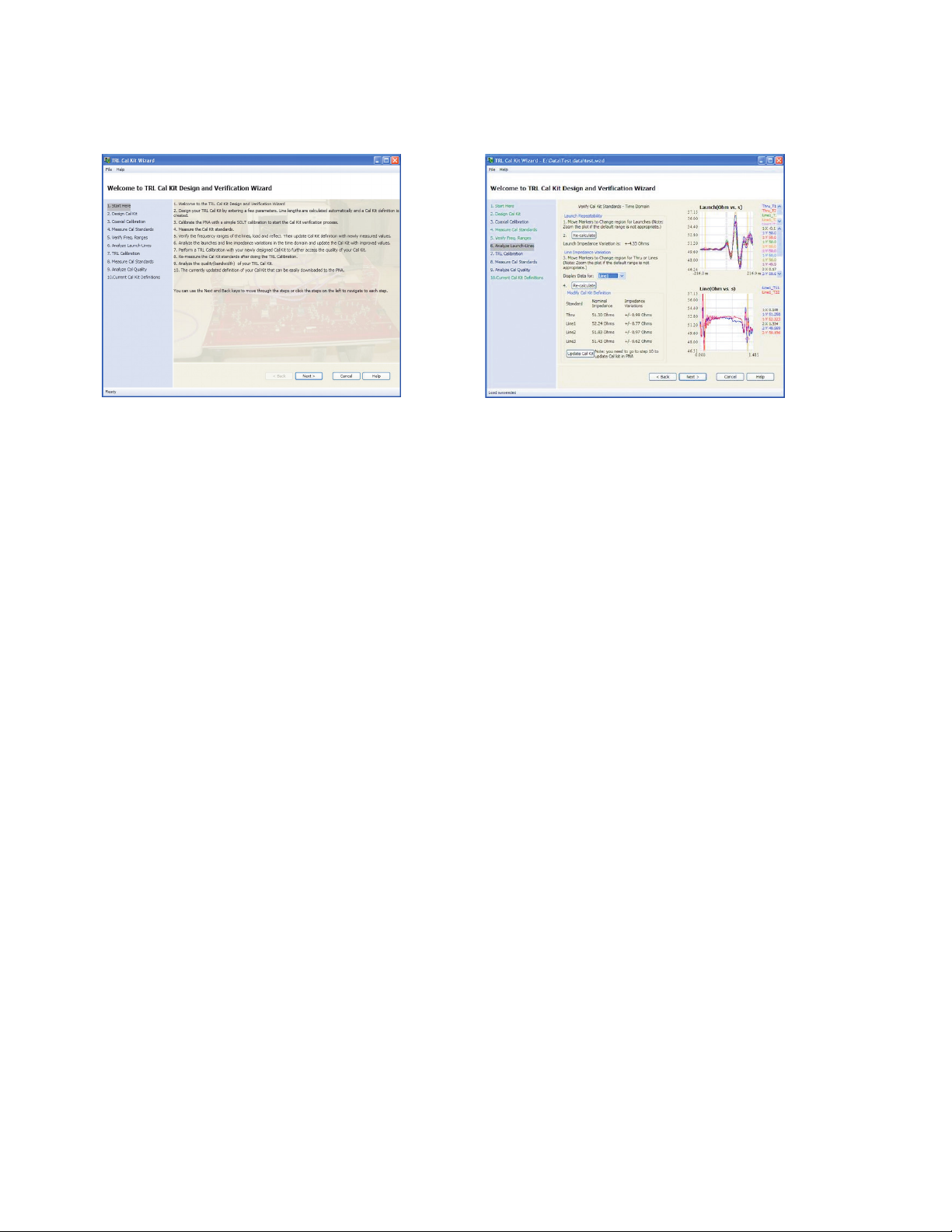
Figure 29. The TRL Calibration Wizard in PLTS N1930B-5TP option
is an industry fi rs t for enabling complex vector network analyzer
error correction in an easy to use format for PCB fixtures.
Keysight has developed a breakthrough signal integrity
software tool that enables digital interconnect designers
never before available capabilities. The Physical Layer Test
System (PLTS) version 5.2 software Option N1930B-5TP
will incorporate three new advanced calibration tools that
optimize the design of high speed connectors, cables,
backplanes and printed circuit boards. The PLTS Option
N1930B-5TP provides advanced calibration wizards for a
complete suite of signal integrity capability including:
– Thru-Reflect-Line (TRL) calibration wizard for design
and validation of customer-built test fixtures
– Differential crosstalk calibration wizard that takes
into account coupling effects of differential transmission lines on fixtures for extremely accurate error
correction
– Automatic fixture removal feature that requires only
a symmetric “Thru” structure is measured for quick
and easy fixture de-embedding
Figure 30. The TRL Calibration Wizard has a step-by-step
procedure for validating the customer built TRL fi xture and verifies
the high frequency performance level in a quantitative fashion.
TRL calibration wizard
Many high-speed digital labs today must design test
fixtures for data rates above 5 Gbps. More advanced
design techniques must be used when designing test
fixtures for these sensitive s-parameter measurements.
The TRL calibration process has been the traditional
method for microwave engineers for decades to precisely
locate the measurement reference plane. However this
advanced technique has been out of reach for most digital
laboratories due to complexity. This is no longer the case.
The TRL calibration wizard is the world’s first software
tool that enables the design and validation of a PCB-based
TRL calibration kit. This step-by-step process easily guides
you carefully through the normally tedious and error prone
process of TRL fixture design, saving at least 50% of the
design cycle time from beginning to end, thus reducing the
number of board spins. Now, with TRL calibration wizard,
you can invoke the wizard to define the line lengths for
each calibration structure. After sending the board layout
details to a PCB house for manufacture, the wizard will
measure the newly designed TRL test fixture to verify that
it will work properly at the desired high frequency range.
23
Page 24
Advanced Calibration Software Option N1930B-5xP (continued)
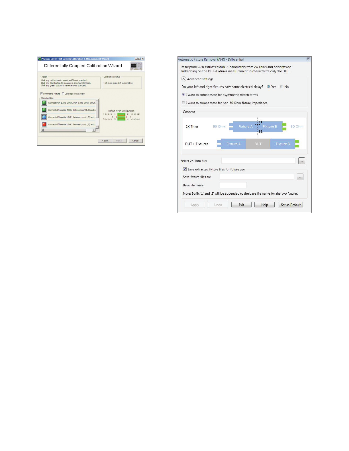
Figure 31. One of the most difficult error corrections to do is
remove differential coupling in test fixtures. The Differential
Calibration Wizard is the first tool of its kind to perform a
correction to remove error due to this type of coupling.
Differential crosstalk calibration wizard
When designing test fixturing for interconnect
characterization, the age old question is “How should I
route my test fixture transmission lines, single-ended or
differential?” Some engineers correctly route them singleendedly, some erroneously route them differentially and
some just don’t care. The biggest mistake is to route
differentially and ignore the coupling effects. As long as a
calibration algorithm is used to remove coupling effects,
then this test fixture design flaw can be easily remedied.
The differential crosstalk calibration wizard in PLTS 5.2
Option 5TP will automatically measure these coupling
effects and remove them from the measurement using a
proprietary calibration algorithm. Some steps in the wizard
can be eliminated if the fixture is symmetric from front to
back, thereby optimizing the algorithm in real time. There are
test fixture amplitude measurement errors as large as 25 dB
that have been fixed by the differential crosstalk calibration
wizard.
Automatic xture removal
It can sometimes be a complicated process to achieve
accurate calibrations with a vector network analyzer (VNA).
The time consuming part of the measurement sequence is
often not the measurement itself, but the calibration. For
those who feel that way, we have created the Automatic
Figure 32. Automatic Fixture Removal (AFR) is the industry standard for
de-embedding test fixtures without having the fixture S-parameters.
Fixture Removal. There are two ways to accomplish AFR:
the legacy 2X Thru method introduced in PLTS 2011 or
the new 1-port open method introduced in PLTS 2014. The
legacy method is a simple process that entails measuring a
user created 2X Thru calibration PCB coupon (two fixtures
end-to-end). This 2X Thru coupon trace can be built on test
fixtures themselves or on a separate Cal board. In either
case, as soon as this measurement is input into the wizard
and the total measurement of the DUT plus fixtures is in
the active window of the wizard, then a simple click on the
“Apply” button and the fixture is accurately removed. The
resultant accuracy is better than a TRL calibration. It is
simple, fast AND accurate. For PLTS 2014, the 1-port AFR
has been greatly enhanced to allow the test fixture itself
to be used as a 1-port open cal structure. This means that
AFR can now accommodate any application for high-speed
signal integrity applications.
24
Page 25

Advanced Calibration Software Option N1930B-5xP (continued)
Making VNAs easier than TDRs
It has often been stated that VNAs are extremely accurate
at the cost of being complicated. This is possibly true
if the right tools are not at your disposal. Well, now the
right toolset is available at the right time; just as data
rates are driven to 5 Gbps and higher. No longer do you
need to settle for the –40 dB dynamic range of a TDR
when you have a VNA toolset that makes high dynamic
range measurements a simple task. The PLTS 2014 Option
N1930B-5TP is exactly what you’ve been waiting for.
PLTS application software uses new licensing
capabilities. Besides fixed license and networkable
FLEXlm licensing on a shared server, there is also
a transportable USB key. The summary of the three
licensing options are as follows:
Option xFP Fixed license (default).
Fixed licenses are locked to a single PC through its host
ID (e.g., the MAC address) with or without connected
system hardware. Fixed licenses do not require any
networking or license server processes. A fixed license
is also known as a node-locked license.
Web resources
Visit our Web sites for additional product and literature
information.
www.keysight.com/find/plts
www.keysight.com/find/ena
www.keysight.com/find/pna
www.keysight.com/find/multiport
www.keysight.com/find/ecal
Option xNP Networkable license.
Networkable licenses allow users to share a single
license, or multiple licenses, over a network. The
application software may be installed on an unlimited
number of PCs with or without connected system
hardware. The number of available licenses determines
the number of concurrent users. Networkable licenses
require a license server and a TCP/IP (or IPX/
SPX) connection between clients and server(s). A
networkable license is also known as a floating license.
Option xTP Transportable license.
Transportable licenses are locked to a USB key that can
be shared among different PCs.
Important licensing notes:
1. File import, file export, calibrations, and
measurements greater than
4 ports requires one of the following PLTS options:
7NP, 7FP, or 7TP.
2. For 4-port calibrations option 550 is required on the
PNA firmware. For greater than 4-port calibrations
option 551 is required on the PNA firmware.
3. See configuration guide information contained in this
Technical Overview for further details.
25
Page 26

26 | Keysight | Physical Layer Test System (PLTS) 2014 - Technical Overview
myKeysight
www.keysight.com/find/mykeysight
A personalized view into the information most relevant to you.
Three-Year Warranty
www.keysight.com/find/ThreeYearWarranty
Keysight’s commitment to superior product quality and lower total cost
of ownership. The only test and measurement company with three-year
warranty standard on all instruments, worldwide.
Keysight Assurance Plans
www.keysight.com/find/AssurancePlans
Up to five years of protection and no budgetary surprises to ensure your
instruments are operating to specification so you can rely on accurate
measurements.
www.keysight.com/go/quality
Keysight Technologies, Inc.
DEKRA Certified ISO 9001:2008
Quality Management System
Keysight Channel Partners
www.keysight.com/find/channelpartners
Get the best of both worlds: Keysight’s measurement expertise and product
breadth, combined with channel partner convenience.
www.keysight.com/find/plts
For more information on Keysight
Technologies’ products, applications or
services, please contact your local Keysight
office. The complete list is available at:
www.keysight.com/find/contactus
Americas
Canada (877) 894 4414
Brazil 55 11 3351 7010
Mexico 001 800 254 2440
United States (800) 829 4444
Asia Pacic
Australia 1 800 629 485
China 800 810 0189
Hong Kong 800 938 693
India 1 800 112 929
Japan 0120 (421) 345
Korea 080 769 0800
Malaysia 1 800 888 848
Singapore 1 800 375 8100
Taiwan 0800 047 866
Other AP Countries (65) 6375 8100
Europe & Middle East
Austria 0800 001122
Belgium 0800 58580
Finland 0800 523252
France 0805 980333
Germany 0800 6270999
Ireland 1800 832700
Israel 1 809 343051
Italy 800 599100
Luxembourg +32 800 58580
Netherlands 0800 0233200
Russia 8800 5009286
Spain 0800 000154
Sweden 0200 882255
Switzerland 0800 805353
Opt. 1 (DE)
Opt. 2 (FR)
Opt. 3 (IT)
United Kingdom 0800 0260637
For other unlisted countries:
www.keysight.com/find/contactus
(BP-09-04-14)
This information is subject to change without notice.
© Keysight Technologies, 2012 - 2014
Published in USA, August 2, 2014
5989-6841EN
www.keysight.com
 Loading...