

Page 1
Keysight Technologies
HMMC-5027 2 to 26.5 GHz
Medium Power Amplier
IGG7-8002
Data Sheet
Page 2
02 | Keysight | HMMC-5027 2 to 26.5 GHz Medium Power Amplier - Data Sheet
Description
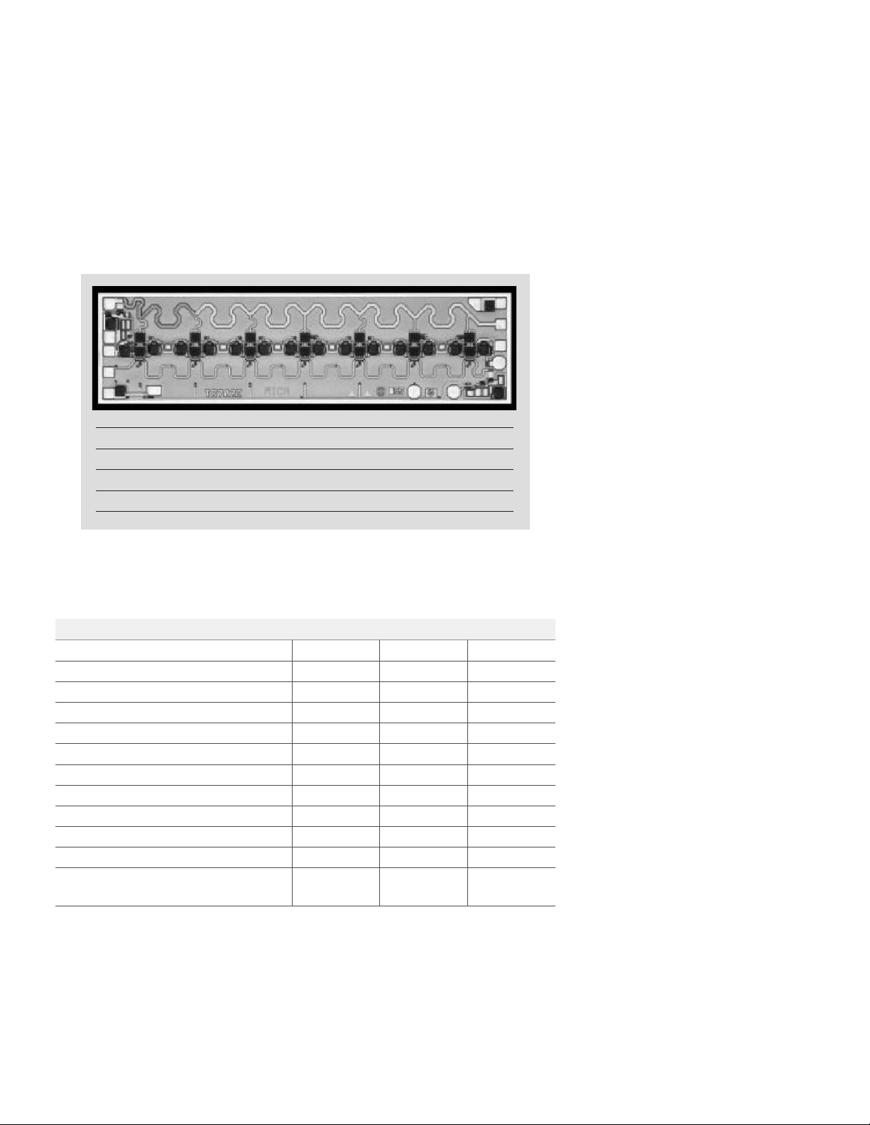
The HMMC-5027 is a broadband GaAs MMIC traveling wave amplier designed for medium output power and moderate gain over the full 2 to 26.5 GHz frequency range. Seven
MES-FET cascode stages provide a at gain response, making the HMMC-5027 an ideal
wideband power block. Optical lithography is used to produce gate lengths of ≈0.5 μm.
The HMMC-5027 incorporates advanced MBE technology, Ti-Pt-Au gate metallization,
silicon nitride passivation, and polyimide for scratch protection.
Chip size 2980 × 770 μm (117.3 × 30.3 mils)
Chip size tolerance ± 10 μm (± 0.4 mils)
Chip thickness 127 ± 15 μm (5 ± 0.6 mils)
Pad dimensions 75 × 75 μm (2.95 × 2.95 mils), or larger
Features
– Wide-frequency range:
2 to 26.5 GHz
– Moderate gain:
7 dB
– Gain atness:
± 1 dB
– Return loss:
Input: –13 dB, Output: –11 dB
– Low-frequency operation capability:
< 2 GHz
– Gain control:
30 dB dynamic range
– Moderate power:
20 GHz:
P
P
26.5 GHz:
P
P
: 22 dBm
–1 dB
: 24 dBm
sat
: 19 dBm
–1 dB
: 21 dBm
sat
Absolute Maximum Ratings
1
Symbol Parameters/conditions Min Max Units
V
DD
I
DD
V
G1
I
G1
V
G2
I
G2
P
DC
P
in
T
ch
T
case
T
stg
T
max
Positive drain voltage 8.0 Volts
Total drain current 300 mA
First gate voltage –5 0 Volts
First gate current –1 +1 mA
Second gate voltage –2.5 +5 Volts
Second gate current –25 mA
DC power dissipation 2.4 Watts
CW input power 23 dBm
Operating channel temp. +150 ºC
Operating case temp. –55 ºC
Storage temperature –65 +165 ºC
Maximum assembly temp.
300 ºC
(for 60 seconds maximum)
1. Operation in excess of any one of these conditions may result in permanent damage to this device. TA
= 25 °C except for T
, T
, and T
ch
stg
max
.
Page 3

03 | Keysight | HMMC-5027 2 to 26.5 GHz Medium Power Amplier - Data Sheet
DC Specications/Physical Properties
1
Symbol Parameters/conditions Min Typ Max Units
IDSS Saturated drain current (V
V
p
V
G2
IDSOFF (V
IDSOFF (V
θ
ch–bs
1. Measured in wafer form with T
RF Specications
First gate pinch-off voltage (VDD = 8.0 V, IDD = 30 mA, VG2 = open circuit) –2.2 –1.3 –0.5 volts
Second gate self-bias voltage (VDD = 8.0 V, VG1 = 0.0 V)
) First gate pinch-off current (VDD = 8.0 V, VG1 = –3.5 V, VG2 = open circuit) 7 mA
G1
) Second gate pinch-off current (VDD = 5.0 V, VG1 = 0.0 V, VG2 = –3.5 V) 10 mA
G2
Thermal resistance (T
chuck
1
(VDD = 8.0 V, IDD(Q) = 250 mA or I
Symbol Parameters/conditions
= 8.0 V, VG1 = 0.0 V, VG2 = open circuit) 200 300 500 mA
DD
1.8
(0.27 × V
= 25 °C) 28 °C/W
backside
= 25 °C. (except θ
, Zin = Zo = 50 Ω)
DSS
ch–bs
).
)
DD
Min Typ Max Units
volts
BW Guaranteed bandwidth2 2 26.5 GHz
S21 Small signal gain 6 7 dB
ΔS21 Small signal gain atness ±0.8 dB
RLin Input return loss –13 –10 dB
RLout Output return loss –11 –10 dB
S12 Reverse isolation –28 –25 dB
P–1 dB Output power at 1 dB gain compression 16.5 19 dBm
Psat Saturated output power 18.5 21 dBm
H2
H3
Second harm. (2 < ƒo < 20),
[Po(ƒo) = 21 dBm or P–1 dB, whichever is less]
Third harm. (2 < ƒo < 20),
[Po(ƒo) = 21 dBm or P–1 dB, whichever is less]
–21 –18 dBc
–32 –18 dBc
NF Noise gure 11 dB
1. Small-signal data measured in wafer form with Tchuck = 25 °C. Large-signal data measured on individual devices mounted in an 83040 Series Modular
Microcircuit Package @ TA = 25 °C.
2. Performance may be extended to lower frequencies through the use of appropriate of f-chip circuitry. Upper corner frequency –30 GHz.
Page 4

04 | Keysight | HMMC-5027 2 to 26.5 GHz Medium Power Amplier - Data Sheet
Applications
The HMMC-5027 series of traveling wave ampliers are designed for use as general purpose wideband power stages in communication systems and microwave instrumentation.
They are ideally suited for broadband applications requiring a at gain response and
excellent port matches over a 2 to 26.5 GHz frequency range. Dynamic gain control and
low-frequency extension capabilities are designed into these devices.
Biasing and Operation
These ampliers are biased with a single positive drain supply (VDD) and a single negative
gate supply (V
I
= 250 mA or I
DD
biased between 0 V and –0.6 V. No other bias supplies or connections to the device are
required for 2 to 26.5 GHz operation. The gate voltage (V
drain voltage (V
down. See Figure 3 for assembly information.
The HMMC-5027 is a DC coupled amplier. External coupling capacitors are needed on
RF
and RF
IN
the lowest operating frequency.
). The recommended bias conditions for the HMMC-5027 are VDD = 8.0 V,
G1
, whichever is less. To achieve this drain current level, VG1 is typically
DSS
) MUST be applied prior to the
G1
) during power up and removed after the drain voltage during power
DD
ports. The drain bias pad is connected to RF and must be decoupled to
OUT
The auxiliary gate and drain contacts are provided when performance below 1 GHz is
required. Connect external capacitors to ground to maintain input and output VSWR at
low frequencies (see Additional References). Do not apply bias to these pads.
The second gate (V
) can be used to obtain 30 dB (typical) dynamic gain control. For
G2
normal operation, no external bias is required on this contact and its selfbias potential is
between +1.5 and +2.5 volts. Applying an external bias between its open circuit potential
and –2.5 volts will adjust the gain while maintaining a good input/output por t match.
Assembly Techniques
GaAs MMICs are ESD sensitive. ESD preventive measures must be employed in all as-
pects of storage, handling, and assembly.
MMIC ESD precautions, handling considerations, die attach and bonding methods are
critical factors in successful GaAs MMIC performance and reliability.
GaAs MMIC ESD, Die Attach and Bonding Guidelines - Application Note, 5991-348 4EN
provides basic information on these subjects.
Additional References:
TC700/702 Traveling Wave Amplier Environmental Data - Technical Overview,
5991-3553EN
GaAs MMIC TWA Users Guide - Application Note, 5991-3545EN
Page 5
05 | Keysight | HMMC-5027 2 to 26.5 GHz Medium Power Amplier - Data Sheet
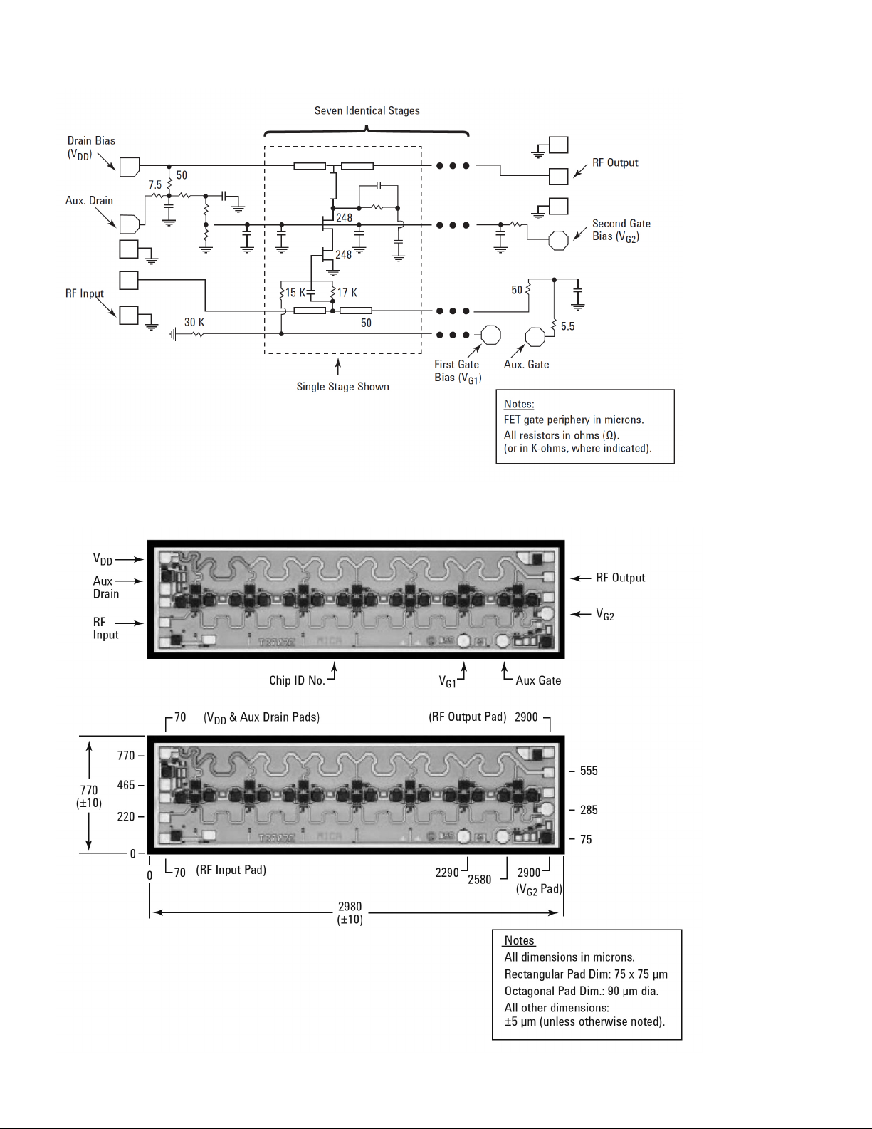
Figure 1. Schematic
Figure 2. Bond pad locations
Page 6
06 | Keysight | HMMC-5027 2 to 26.5 GHz Medium Power Amplier - Data Sheet
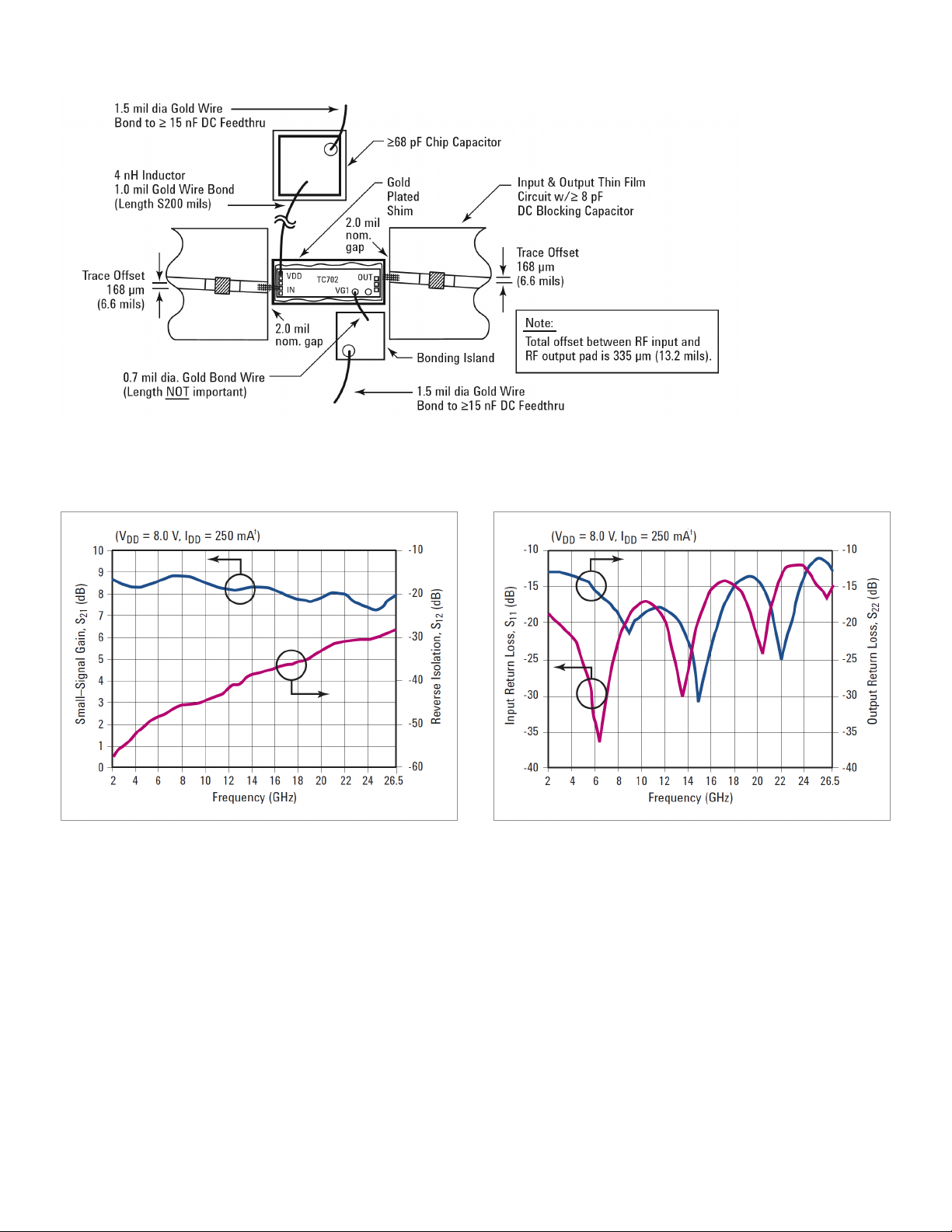
Figure 3. Assembly diagram (for 2.0 to 26.5 GHz operation)
Figure 4. Typical gain and reverse isolation vs. frequency Figure 5. Typical input and output return loss vs. frequency
Page 7

07 | Keysight | HMMC-5027 2 to 26.5 GHz Medium Power Amplier - Data Sheet
Typical S–Parameters
(T
= 25 °C, VDD = 8.0 V, IDD = 250 mA or I
chuck
1
, whichever is less, Zin = Z
DSS
= 50 Ω)
out
Freq. S11 S12 S21 S22
(GHz) dB Mag Ang dB Mag Ang dB Mag Ang dB Mag Ang
2.0 –18.7 0 .116 –139 . 5 –57.7 0.0013 –165.2 8.7 2.717 116.6 –13 .0 0.223 173.5
3.0 –2 0.1 0.099 –159. 0 –54.9 0.0018 144.2 8.4 2.635 94.8 –13 . 0 0.224 150.0
4.0 –21.5 0.084 –175 .7 –52.0 0.0025 154.0 8.3 2.612 72.0 –13.5 0.212 12 7.1
5.0 –24.6 0.059 167.8 –49.9 0.0032 111.3 8.4 2.634 48.2 –14.0 0.200 101.6
6.0 –32.0 0.025 16 7.4 –48.2 0.0039 91.3 8.6 2.699 23.3 –15.3 0 .17 1 71.7
7.0 –30.8 0.029 –94.8 –46.9 0.0045 74.9 8.8 2.763 –3.5 –16 .9 0 .14 3 39.5
8.0 –22.7 0.073 –103 . 2 –45.5 0.0053 21.0 8.8 2.768 –30.9 –18. 4 0.120 – 2.2
9.0 –18.9 0.114 –121.5 –45.2 0.0055 10.3 8.8 2.74 4 –58.9 –21.3 0.086 –46.9
10.0 –17. 2 0.137 –142.6 –44.7 0.0058 –15.5 8.5 2.673 –85.9 –18. 9 0.114 –90.7
11.0 –17.4 0 .13 5 –16 3.9 –43.5 0.0067 –33.4 8.3 2.608 –112.5 –17.9 0.127 –129.6
12.0 –19.3 0 .10 8 175.6 – 41.5 0.0084 –45.4 8.2 2.564 –138. 5 –18.2 0 .12 3 –162.6
13.0 –25.6 0.052 170.3 –40.6 0.0093 –75.8 8.2 2.578 –16 4.9 –19 . 3 0.10 8 163.4
14.0 –2 7. 0 0.045 –113.0 –38.6 0.0118 –95.9 8.3 2.610 167.1 –22.1 0.078 126.5
15.0 –19.2 0.109 –111. 0 –37.8 0.0129 –124 .7 8.3 2.605 138.4 –31.2 0.028 56.7
16.0 –15.6 0.16 7 –127.9 –37.1 0.0139 –149.1 8.2 2. 574 108.8 –23.5 0.067 –33.3
17. 0 –14.3 0.19 3 –14 8.4 –36.3 0.0153 –174.5 8.0 2.510 79.7 –18.1 0.124 –80.7
18.0 –14.8 0 .18 2 –16 6.6 –35.8 0.0163 16 4.1 7. 8 2.444 50.9 –15 . 2 0.174 –115.2
19.0 –17.1 0.14 0 –179. 3 –34.7 0.0185 141.5 7.7 2.418 22.1 –13.7 0.207 –147. 6
20.0 –21. 4 0.086 –166.2 –32.9 0.0227 112.6 7.8 2.466 –7.5 –13 . 9 0.202 17 7. 9
21.0 –18.4 0.121 –129. 5 –31.6 0.0262 80.7 8.1 2.527 –39.9 –16.8 0.14 5 136.7
22.0 –13.8 0.205 –137.2 –30.9 0.0285 42.7 8.0 2.512 –74.0 –25.3 0.054 66.9
23.0 –12.1 0.247 –152.7 –30.6 0.0296 13.3 7.6 2.395 –10 8 .4 –19 . 8 0.10 2 –56.2
24.0 –12.3 0.24 4 –169 . 8 –30.3 0.0304 –15.5 7.4 2.344 –142.5 –13.7 0.207 –103. 5
25.0 –14 .7 0.184 –175. 8 –29.7 0.0329 –44.9 7.3 2.315 –175.6 –11.3 0.272 –136.7
26.0 –16.7 0 .146 –14 9.3 –28.5 0.0375 –78.1 7.9 2.469 148.1 –11.7 0.259 –171.3
26.5 –14.1 0 .197 –141.6 –28.0 0.0399 –98.5 8.0 2.503 126.9 –13.0 0.223 172.3
1. Data obtained from on-wafer measurements.
Page 8
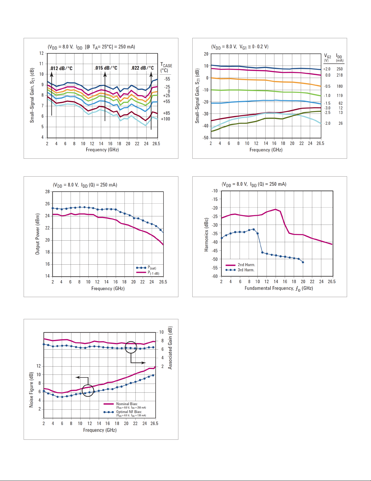
08 | Keysight | HMMC-5027 2 to 26.5 GHz Medium Power Amplier - Data Sheet
Figure 6. Typical small-signal gain vs. temperature
Figure 8. Typical 1 dB gain compression and saturated output power
vs. frequency
Figure 7. Typical gain vs. second gate control voltage
Figure 9. Typical second and third harmonics vs. fundamental frequency at
Pout = +21 dBm
Figure 10. Typical noise gure performance
Notes
All data measured on individual devices mounted in an 83040
Series Modular Microcircuit Package @ TA = 25 °C (except where
noted).
This data sheet contains a variety of typical and guaranteed
performance data. The information supplied should not be interpreted as a complete list of circuit specications. Customers
considering the use of this, or other Keysight Technologies Inc.
TCA GaAs ICs, for their design should obtain the current production specications from Keysight TCA Marketing. In this data
sheet the term typical refers to the 50th percentile performance.
For additional information contact Keysight TCA Marketing at
707-577-4482.
Page 9

09 | Keysight | HMMC-5027 2 to 26.5 GHz Medium Power Amplier - Data Sheet
myKeysight
www.keysight.com/find/mykeysight
A personalized view into the information most relevant to you.
Three-Year Warranty
www.keysight.com/find/ThreeYearWarranty
Keysight’s commitment to superior product quality and lower total cost
of ownership. The only test and measurement company with three-year
warranty standard on all instruments, worldwide.
Keysight Assurance Plans
www.keysight.com/find/AssurancePlans
Up to five years of protection and no budgetary surprises to ensure your
instruments are operating to specification so you can rely on accurate
measurements.
www.keysight.com/quality
Keysight Technologies, Inc.
DEKRA Certified ISO 9001:2008
Quality Management System
Keysight Channel Partners
www.keysight.com/find/channelpartners
Get the best of both worlds: Keysight’s measurement expertise and product
breadth, combined with channel partner convenience.
www.keysight.com/find/mmic
For more information on Keysight
Technologies’ products, applications or
services, please contact your local Keysight
office. The complete list is available at:
www.keysight.com/find/contactus
Americas
Canada (877) 894 4414
Brazil 55 11 3351 7010
Mexico 001 800 254 2440
United States (800) 829 4444
Asia Pacic
Australia 1 800 629 485
China 800 810 0189
Hong Kong 800 938 693
India 1 800 112 929
Japan 0120 (421) 345
Korea 080 769 0800
Malaysia 1 800 888 848
Singapore 1 800 375 8100
Taiwan 0800 047 866
Other AP Countries (65) 6375 8100
Europe & Middle East
Austria 0800 001122
Belgium 0800 58580
Finland 0800 523252
France 0805 980333
Germany 0800 6270999
Ireland 1800 832700
Israel 1 809 343051
Italy 800 599100
Luxembourg +32 800 58580
Netherlands 0800 0233200
Russia 8800 5009286
Spain 0800 000154
Sweden 0200 882255
Switzerland 0800 805353
Opt. 1 (DE)
Opt. 2 (FR)
Opt. 3 (IT)
United Kingdom 0800 0260637
For other unlisted countries:
www.keysight.com/find/contactus
(BP-07-10-14)
This information is subject to change without notice.
© Keysight Technologies, 2013 - 2014
Published in USA, August 3, 2014
5989-6208EN
www.keysight.com
 Loading...