

Page 1
Keysight Technologies
HMMC-5025 2-50 GHz
Distributed Amplier
1GG6-8000
Data Sheet
Features
– Frequency range:
2-50 GHz
– Small signal gain:
8.5 dB
– P
– Noise gure:
5 dB @ 2-35 GHz
7 dB @ 35-50 GHz
– Return loss:
In/out: < –10 dB
– 30 dB gain control
@ 40 GHz: 12 dBm
–1 dB
Page 2
02 | Keysight | HMMC-5025 2-5 0 GHz Dis tributed Amplier – Data Sheet
Description
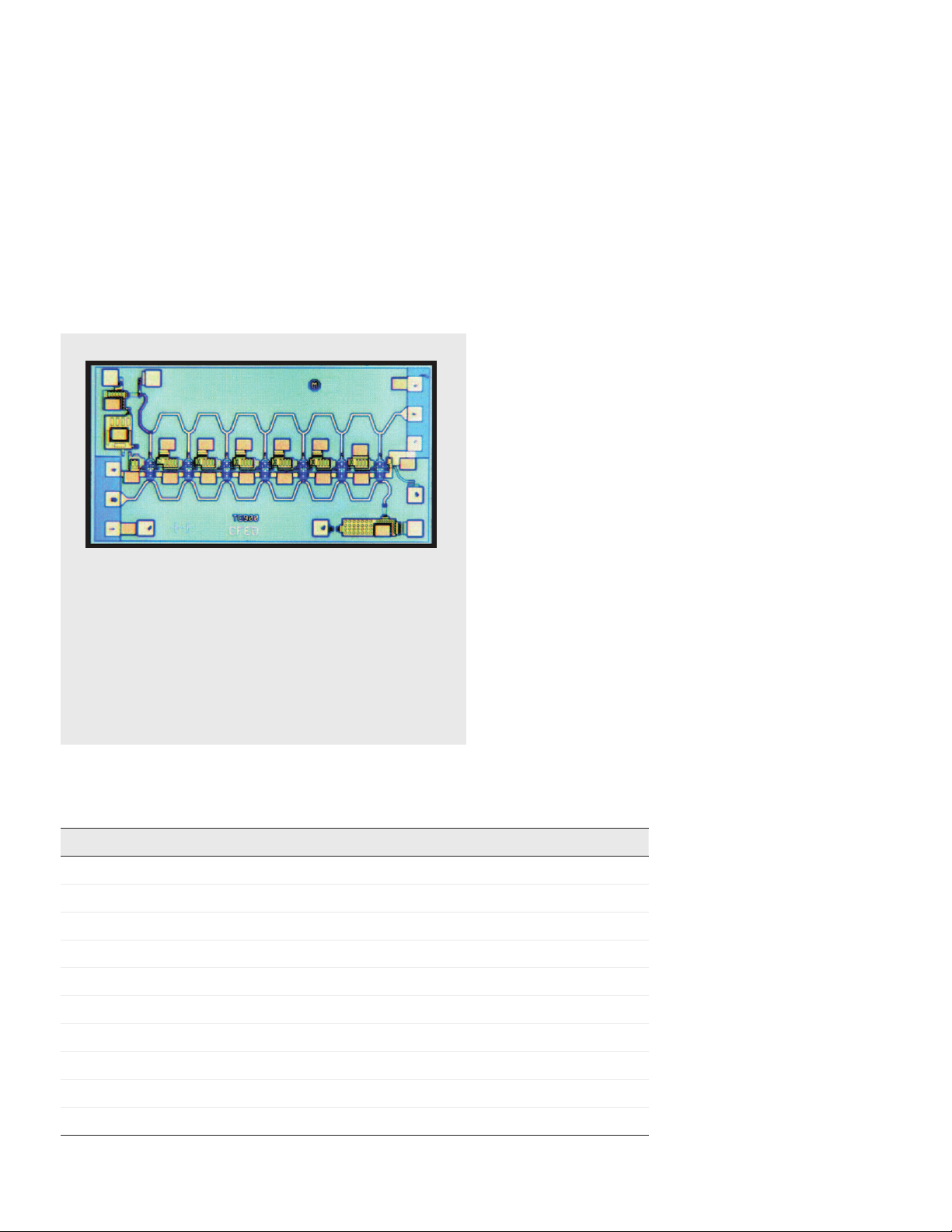
The HMMC-5025 was designed as a generic wide band distributed amplier, covering the
frequency span 2-50 GHz. It consists of seven stages. Each stage is made up of two
cascaded FETs with gate peripheries of 48 μm per FET. Both input and output ports were
designed to provide 50 Ohm terminations. Bonding pads are provided in the layout to allow
amplier operation at frequencies lower than 2 GHz by means of external circuit components.
The amplier is biased with a single positive drain supply (VDD) and a single negative gate
supply (VG1). A second gate connection is provided for external gain control applications.
Chip Size:
1720 × 920 μm (67.7 × 36.2 mils)
Chip Size Tolerance:
±10 μm (±0.4 mils)
Chip Thickness:
127 ± 15 μm (5 ±0.6 mils)
Pad Dimensions:
80 × 80 μm (3.2 × 3.2 mils)
Absolute Maximum Ratings
1
Symbol Parameters/conditions Min. Max. Units
V
DD
I
DD
V
G1
V
G2
Positive drain voltage 7.0 volts
Total drain current 170 mA
First gate voltage –3.5 0 volts
Second gate voltage –3.0 +3.0 volts
PDC power DC power dissipation 1.2 watts
P
T
T
T
T
in
ch
case
stg
max
CW input power 20 dBm
Operating channel temperature 150 °C
Operating case temperature –55 °C
Storage temperature –65 165 °C
Maximum assembly temperature (for 60 seconds maximum) 300 °C
1. Operation in excess of any one of these conditions may result in permanent damage to this
device. TA = 25 °C except for Tch, T
stg
, and T
max
.
Page 3

03 | Keysight | HMMC-5025 2-5 0 GHz Dis tributed Amplier – Data Sheet
DC Specifications/Physical Properties
1
Symbol Parameters/conditions Min. Typ. Max. Units
I
DSS
V
P
V
G2
I
DSOFF(VG1
I
DSOFF(VG2
Θ
ch-bs
) First gate pinch-off current (VDD = 5.0 V, VG1 = –3.5 V, VG2 = open circuit) 6 10 mA
) Second gate pinch-off current (VDD = 5.0 V, IDD = 75 mA, VG2 = –2.5 V) 10 mA
Saturated drain current (VDD = 5.0 V, VG1 = 0.0 V, VG2 = open circuit) 130 150 170 mA
First gate pinch-off voltage (VDD = 5.0 V, IDD = 15 mA, VG2 = open circuit) –1.7 –0.5 Volts
Second gate self-bias voltage (VDD = 5.0 V, IDD = 75 mA) 2 Volts
Thermal resistance (T
= 25 °C) 63 °C/Watt
backside
1. Measured in wafer form with T
RF Specications
1
= 25 °C. (Except Θ
chuck
ch-bs
)
(VDD = 5.0 V, IDD(Q) = 75 mA, Zin = Zo = 50 Ω)
Symbol Parameters/conditions Min. Typ. Max. Units
BW Guaranteed bandwidth
2
2 50 GHz
Gain Small signal gain 7.0 8.5 dB
∆Gain Small signal gain atness ±0.75 ±1.5 dB
RL
RL
in
out
Input return loss 10 15 dB
Output return loss 10 15 dB
Isolation Reverse isolation 20 30 dB
P
–1 dB
P
sat
H
H
2
3
Output power at 1 dB gain Compression @ 40 GHz 12 dBm
Saturated output power @ 40 GHz 16 dBm
Second harmonic (2 < ƒo< 26) (Po(ƒo) = 10 dBm –35 dBc
Third harmonic (2 < ƒo< 26) (Po(ƒo) = 10 dBm –25 dBc
NF Noise gure (2-35 GHz) 5.0 dB
NF Noise gure (35-50 GHz) 7.0 dB
1. Small-signal data measured in wafer form with T
2. Performance may be extended to lower frequencies through the use of appropriate off-chip circuitry.
= 25 °C. Harmonic data measured on individual device mounted in a microcircuit package @ TA = 25 °C.
chuck
Page 4

04 | Keysight | HMMC-5025 2-5 0 GHz Dis tributed Amplier – Data Sheet
Applications
The HMMC-5025 traveling wave amplier is designed for use as a general purpose
wideband power stage in communication systems, and microwave instrumentation,
and optical systems. It is ideally suited for broadband applications requiring a at gain
response and excellent port matches over a 2 to 50 GHz frequency range. Dynamic gain
control and lowfrequency ex tension capabilities are designed into these devices.
It is characteristic of traveling wave ampliers that S22 tends to 0 dB and greater out
of band. This is the design trade-off for the broadband performance of TWAs. As a
consequence, TWAs are not necessarily uncondtionally stable out of band. This means
that if a TWA is followed by a reective low-pass lter, oscillations can occur. This
phenomenon is exacerbated by low temperature where the gain is higher. More data will
follow on individual devices.
Biasing and Operation
The recommended bias conditions for best performance for the HMMC- 5025 are VDD =
5.0 V, IDD = 75 mA. To achieve these drain current levels, VG1 is typically biased between
–0.2 V and –0.6 V. No other bias supplies or connections to the device are required
for 2 to 50 GHz operation. The gate voltage (VG1) should be applied prior to the drain
voltage (VDD) during power up and removed after the drain voltage during power down.
The HMMC-5025 is a DC coupled amplier. External coupling capacitors are needed on
RFIN and RF
the lowest operating frequency.
The auxiliary gate and drain contacts are provided when performance below 1 GHz is
required. Connect external capacitors to ground to maintain input and output VSWR at
low frequencies (see Additional References). Do not apply bias to these pads.
The second gate (VG2) can be used to obtain 30 dB (typical) dynamic gain control. For
normal operation, no external bias is required on this contact.
ports. The drain bias pad is connected to RF and must be decoupled to
OUT
Assembly Techniques
GaAs MMICs are ESD sensitive. ESD preventive measures must be employed in all
aspects of storage, handling, and assembly.
MMIC ESD precautions, handling considerations, die attach and bonding methods are
critical factors in successful GaAs MMIC performance and reliability.
Keysite Technologies application note, GaAs MMIC ESD, Die Attach and Bonding
Guidelines (literature number 5991- 3484EN) provides basic information on these
subjects.
Additional References:
Keysite Technologies application note, GaAs MMIC TWA Users Guide
(literature number 5991-3545EN).
Page 5
05 | Keysight | HMMC-5025 2-5 0 GHz Dis tributed Amplier – Data Sheet
Low frequency
extension
Aux drain
15
15
8.5
RF input
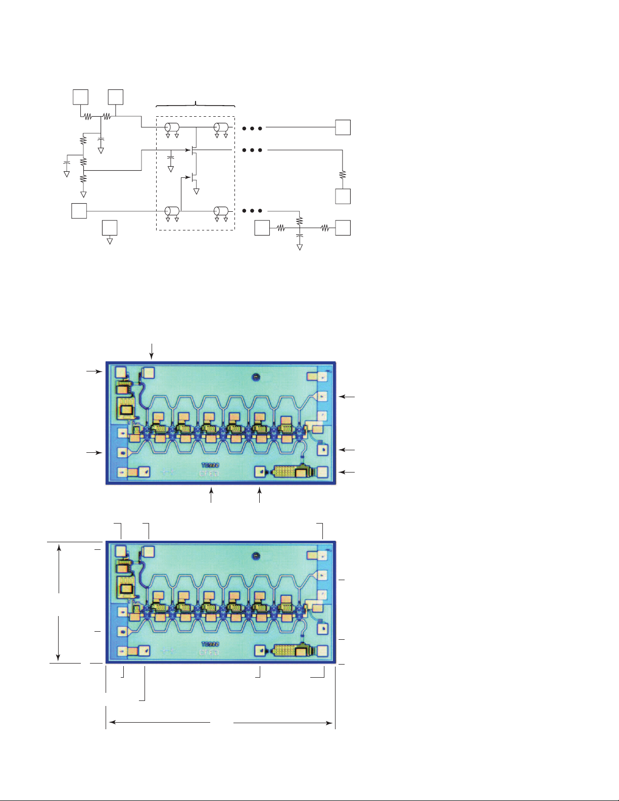
Figure 1. Schematic
470
340
50
GND
Drain
bias
1.5
Seven similar stages
V
DD
Gate
bias
350
50
9.2
RF output
8.5
6
Low frequency
extension
Second gate
bias
Aux gate
920 (±10)
Aux.
drain
RF
input
(Aux V
844
234
DD
0
98
314
pad) (VDD)
114
(RF input)
0
280
(GND pad)
Chip ID no.
1720
(±10)
1160
(V
G1
V
G1
)
RF
output
Aux. 2nd
gate bias
Aux.
gate bias
1625
(RF output)
668
258
90
1630
(Aux gate and
Aux 2nd gate)
Figure 2. Bond pad locations
Page 6
06 | Keysight | HMMC-5025 2-5 0 GHz Dis tributed Amplier – Data Sheet
Input return loss (dB)
Drain bias must be decoupled from
RF to lowest operating frequency.
(AN #56).
100 pF
4 ηH inductor for
operation to 2 GHz
(200 mil bond wire).
Gate is decoupled from RF,
(Bond wire length not important)
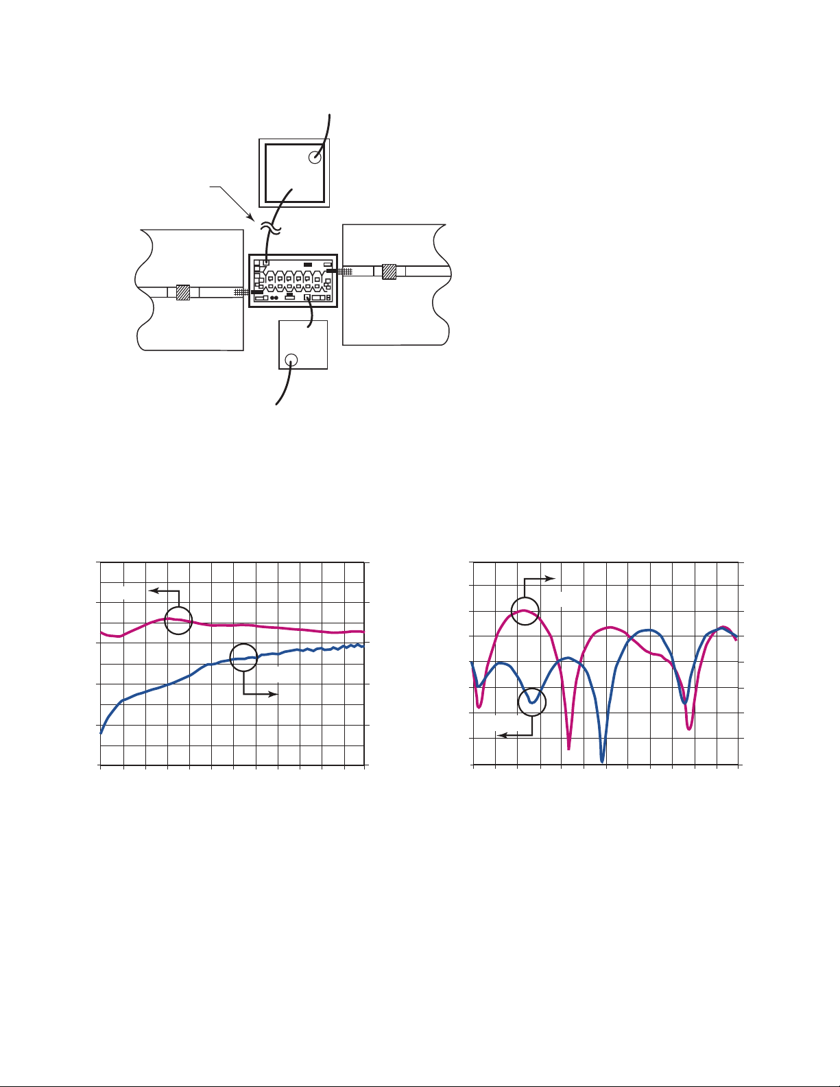
Figure 3. Assembly diagram
VDD = 5.0 V, IDD = 75 mA
12
Gain
10
8
6
Small – signal gain (dB)
4
2
2 6 10 14 18 22 26 30 34 38 42 46 50
(1)
Isolation
Frequency (GHz)
Figure 4. Typical Gain and Reverse isolation vs. Frequency
10
20
30
40
Reverse isolation (dB)
50
60
Figure 5. Typical Input and Output return loss vs. Frequency
VDD = 5.0 V, IDD = 75 mA
5
10
(1)
Output
15
20
25
30
35
Input
40
45
2 6 10 14 18 22 26 30 34 38 42 46 50
Frequency (GHz)
5
10
15
20
25
30
35
Output return loss (dB)
40
45
Page 7

07 | Keysight | HMMC-5025 2-5 0 GHz Dis tributed Amplier – Data Sheet
Typical S–Parameters
(T
= 25 °C, VDD = 5.0 V, I
chuck
Freq. (GHz)
S
1
= 75 mA, Zin = Zo = 50 Ω)
DD
11
S
12
S
21
S
22
dB Mag Ang dB Mag Ang dB Mag Ang dB Mag Ang
2 –24.6 0.059 –150.2 –52.0 0.0025 –110.2 8.5 2.660 147.8 –26.1 0.049 –64.0
3 –29.7 0.033 147.5 –49.1 0.0035 –130.2 8.4 2.630 139.6 –33.8 0.020 –23.6
4 –28.9 0.036 89.0 –47.1 0.004 4 –146.4 8.4 2.630 129.8 –30.1 0.031 43.9
5 –27.0 0.045 56.2 –45.5 0.0053 –161.6 8.4 2.629 119.5 –24.6 0.059 55.9
6 –25.8 0.052 32.6 –4 4.2 0.0061 –176.8 8.4 2.643 108.9 –20.8 0.091 52.1
7 –25.2 0.055 12.7 –43.3 0.0068 169.3 8.5 2.668 98.1 –18.4 0.121 43.8
8 –25.4 0.054 –6.3 –42.6 0.0074 155.6 8.6 2.705 86.9 –16.7 0.147 33.4
9 –26.0 0.050 –25.3 –42.1 0.0078 143.8 8.8 2.743 75.5 –15.6 0.166 22.3
10 –27.4 0.043 –46.3 –41.7 0.0083 132.1 8.9 2.787 63.7 –15.0 0.178 10.7
11 –29.4 0.034 –70.4 –41.4 0.0085 121.9 9.0 2.823 51.6 –14.8 0.182 –0.9
12 –31.7 0.026 –102.9 –40.9 0.0090 112.3 9.1 2.853 39.3 –14.9 0.179 –12.6
13 –33.0 0.022 –145.8 –40.7 0.0093 104.5 9.2 2.874 26.9 –15.4 0.169 –24.2
14 –31.4 0.027 168.6 –40.3 0.0097 95.4 9.2 2.891 14.3 –16.3 0.153 –35.7
15 –29.1 0.035 136.8 –39.7 0.0104 88.5 9.2 2.891 1.8 –17.6 0.131 –47.3
16 –27.0 0.045 113.4 –39.0 0.0112 80.5 9.2 2.884 –10.8 –19.5 0.106 –59.3
17 –25.4 0.053 95.4 –38.4 0.0120 71.9 9.2 2.870 –23.3 –22.2 0.077 –72.0
18 –24.5 0.060 77.9 –37.7 0.0131 62.9 9.1 2.853 –35.7 –26.7 0.046 –86.1
19 –24.1 0.062 62.1 –37.1 0.0140 53.8 9.1 2.836 –48.1 –35.6 0.017 –114.9
20 –24.4 0.061 48.2 –36.3 0.0153 4 4.3 9.0 2.819 –60.3 –35.3 0.017 107.2
21 –25.0 0.056 37.0 –35.3 0.0172 32.7 9.0 2.806 –72.6 –27.0 0.045 80.0
22 –25.6 0.052 22.6 –35.1 0.0176 19.5 8.9 2.798 –84.7 –23.2 0.069 66.2
23 –27.7 0.041 7.2 –34.7 0.0184 8.9 8.9 2.796 –97.1 –21.0 0.089 54.9
24 –30.9 0.028 –8.2 –34.4 0.0191 –2.8 8.9 2.789 –109.5 –19.4 0.107 4 4.2
25 –38.4 0.012 –39.5 –34.3 0.0194 –14.7 8.9 2.789 –121.9 –18.6 0.118 33.6
26 –40.1 0.010 –169.3 –33.9 0.0202 –25.3 8.9 2.789 –134.5 –18.2 0.124 24.2
27 –30.9 0.029 156.0 –33.7 0.0206 –37.0 8.9 2.794 –147.2 –18.2 0.124 15.5
28 –26.0 0.050 138.6 –33.7 0.0206 –48.5 8.9 2.795 –160.1 –18.4 0.120 7.7
29 –23.1 0.070 122.8 –33.4 0.0213 –58.3 8.9 2.787 –173.1 –18.8 0.115 2.1
30 –21.0 0.089 110.2 –33.3 0.0216 –71.3 8.9 2.780 174.0 –19.6 0.105 –3.4
31 –19.8 0.102 95.3 –32.9 0.0228 –81.1 8.9 2.772 160.9 –20.5 0.095 –7.5
32 –18.9 0.114 82.3 –32.5 0.0236 –93.6 8.8 2.768 147.8 –21.3 0.086 –9.1
33 –18.6 0.117 70.4 –32.3 0.024 4 –105.4 8.8 2.762 134.5 –22.4 0.076 –6.4
34 –18.5 0.118 58.6 –32.3 0.024 4 –120.3 8.8 2.752 121.2 –23.0 0.071 –4.7
35 –19.0 0.112 46.2 –31.9 0.0254 –132.8 8.8 2.747 107.8 –23.5 0.067 –3.5
36 –20.0 0.100 35.6 –31.6 0.0264 –146.2 8.8 2.741 94.4 –23.7 0.066 –2.5
37 –21.5 0.084 26.4 –31.5 0.0266 –161.5 8.7 2.735 80.7 –24.4 0.060 –4.3
38 –24.0 0.063 18.8 –31.5 0.0267 –175.1 8.7 2.728 67.0 –25.4 0.054 –8.9
39 –27.6 0.042 18.9 –31.5 0.0266 171.1 8.7 2.723 53.0 –27.1 0.04 4 –11.8
40 –32.9 0.023 46.7 –31.4 0.0270 157.6 8.7 2.711 39.0 –30.4 0.030 –9.1
41 –30.3 0.031 99.2 –31.2 0.0276 140.9 8.6 2.703 24.8 –38.1 0.012 18.9
42 –25.5 0.053 107.1 –31.0 0.0282 125.0 8.6 2.695 10.5 –32.6 0.023 93.1
43 –22.2 0.078 102.7 –31.4 0.0270 115.6 8.6 2.689 –4.0 –26.2 0.049 94.9
4 4 –20.1 0.099 94.4 –31.1 0.0280 101.4 8.6 2.679 –18.1 –22.4 0.076 86.4
45 –19.0 0.112 85.3 –31.3 0.0272 87.2 8.5 2.672 –33.4 –20.2 0.098 75.3
46 –18.6 0.117 76.5 –30.5 0.0297 72.1 8.5 2.676 –48.5 –18.8 0.115 61.6
47 –18.3 0.121 69.8 –30.6 0.0297 49.9 8.6 2.686 –64.0 –18.0 0.126 48.2
48 –18.8 0.115 62.5 –30.7 0.0293 37.8 8.6 2.689 –79.8 –18.3 0.122 28.8
49 –19.3 0.108 59.9 –30.5 0.0300 20.0 8.6 2.691 –96.1 –19.5 0.106 6.1
50 –20.3 0.096 58.9 –30.3 0.0307 2.7 8.6 2.677 –293.0 –21.7 0.082 –22.7
1. Data obtained from on-wafer measurements.
Page 8
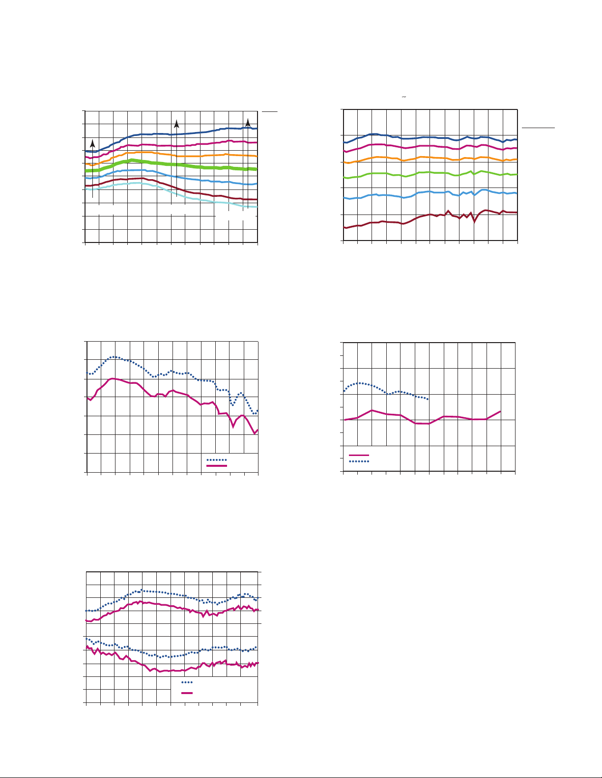
08 | Keysight | HMMC-5025 2-5 0 GHz Dis tributed Amplier – Data Sheet
Small–signal gain, S
(dB)
)
Additional Performance Characteristics
T
(VDD = 5.0 V, IDD = 75 mA)
13
12
11
(dB)
10
21
9
8
7
6
.019 dB/°C
5
Small–signal gain, S
.029 dB/°C
.039 dB/°C
(°C)
-55
-25
+25
+55
+85
+100
A
0
4
3
2 6 10 14 18 22 26 30 34 38 42 46 50
Frequency (GHz)
Figure 6. Typical Small-signal gain vs. Temperature Figure 7. Typical Gain vs. Second gate control voltage
(VDD = 5.0 V, V
G1
-0.66 V)
=
20
10
21
0
-10
-20
-30
2 6 10 14 18 22 26 30 34 38 42 46 50
Frequency (GHz
VG2
(V)
+2.0
-1.0
-1.5
-2.0
-2.5
-3.0
IDD
(mA)
75
59
47
34
24
16
(VDD = 5.0 V, I
18
(Q) = 75 mA)
DD
16
14
12
10
Output power (dBm)
8
6
4
2 6 10 14 18 22 26 30 34 38 42 46 50
Frequency (GHz)
Figure 8. Typical 1 dB Gain compression and Saturated
output power vs. Frequency
6
5
4
3
Noise figure (dB)
2
1
2 4 6 8 10 12 14 16 18 20 22 24 26.5
Nominal Bias:
(V
= 5.0 V, IDD = 75 mA)
DD
Optimal NF Bias:
(V
= 2.25 V, IDD = 26 mA)
DD
Frequency (GHz)
Figure 10. Typical Noise gure performance vs. Frequency
P(sat)
P(-1 dB)
13
11
9
7
5
Associated gain (dB)
(VDD = 5.0 V, I
-10
-15
-20
-25
-30
-35
-40
Harmonics (dBc)
-45
-50
-55
-60
2 3 4 5 6 7 8 9 10 11 12 13 14
DD
2nd Harm.
3rd Harm.
(Q) = 75 mA)
Fundamental frequency, ƒo (GHz)
Figure 9. Typical Second and Third harmonics vs.
Fundamental frequency at P
= 10 dBm
out
Notes
All data measured on individual devices mounted in a 50 GHz test
package TA = 25 °C (except where noted).
This data sheet contains a variety of typical and guaranteed
performance data. The information supplied should not be
interpreted as a complete list of circuit specications. Customers
considering the use of this, or other TCA GaAs ICs, for their
design should obtain the current production specications
from Keysight Technologies, Inc.. In this data sheet the term
typical refers to the 50th percentile performance. For additional
information and support email: [email protected].
Page 9

09 | Keysight | HMMC-5025 2-5 0 GHz Dis tributed Amplier – Data Sheet
myKeysight
www.keysight.com/find/mykeysight
A personalized view into the information most relevant to you.
www.axiestandard.org
AdvancedTCA® Extensions for Instrumentation and Test (AXIe) is an
open standard that extends the AdvancedTCA for general purpose and
semiconductor test. Keysight is a founding member of the AXIe consortium.
ATCA®, AdvancedTCA®, and the ATCA logo are registered US trademarks of
the PCI Industrial Computer Manufacturers Group.
Three-Year Warranty
www.keysight.com/find/ThreeYearWarranty
Keysight’s commitment to superior product quality and lower total cost
of ownership. The only test and measurement company with three-year
warranty standard on all instruments, worldwide.
Keysight Assurance Plans
www.keysight.com/find/AssurancePlans
Up to five years of protection and no budgetary surprises to ensure your
instruments are operating to specification so you can rely on accurate
measurements.
www.keysight.com/quality
Keysight Technologies, Inc.
DEKRA Certified ISO 9001:2008
Quality Management System
Keysight Channel Partners
www.keysight.com/find/channelpartners
Get the best of both worlds: Keysight’s measurement expertise and product
breadth, combined with channel partner convenience.
www.keysight.com/find/mmic
For more information on Keysight
Technologies’ products, applications or
services, please contact your local Keysight
office. The complete list is available at:
www.keysight.com/find/contactus
Americas
Canada (877) 894 4414
Brazil 55 11 3351 7010
Mexico 001 800 254 2440
United States (800) 829 4444
Asia Pacic
Australia 1 800 629 485
China 800 810 0189
Hong Kong 800 938 693
India 1 800 112 929
Japan 0120 (421) 345
Korea 080 769 0800
Malaysia 1 800 888 848
Singapore 1 800 375 8100
Taiwan 0800 047 866
Other AP Countries (65) 6375 8100
Europe & Middle East
Austria 0800 001122
Belgium 0800 58580
Finland 0800 523252
France 0805 980333
Germany 0800 6270999
Ireland 1800 832700
Israel 1 809 343051
Italy 800 599100
Luxembourg +32 800 58580
Netherlands 0800 0233200
Russia 8800 5009286
Spain 0800 000154
Sweden 0200 882255
Switzerland 0800 805353
Opt. 1 (DE)
Opt. 2 (FR)
Opt. 3 (IT)
United Kingdom 0800 0260637
For other unlisted countries:
www.keysight.com/find/contactus
(BP-07-10-14)
This information is subject to change without notice.
© Keysight Technologies, 2013 - 2014
Published in USA, August 3, 2014
5989-6207EN
www.keysight.com
 Loading...