

Page 1
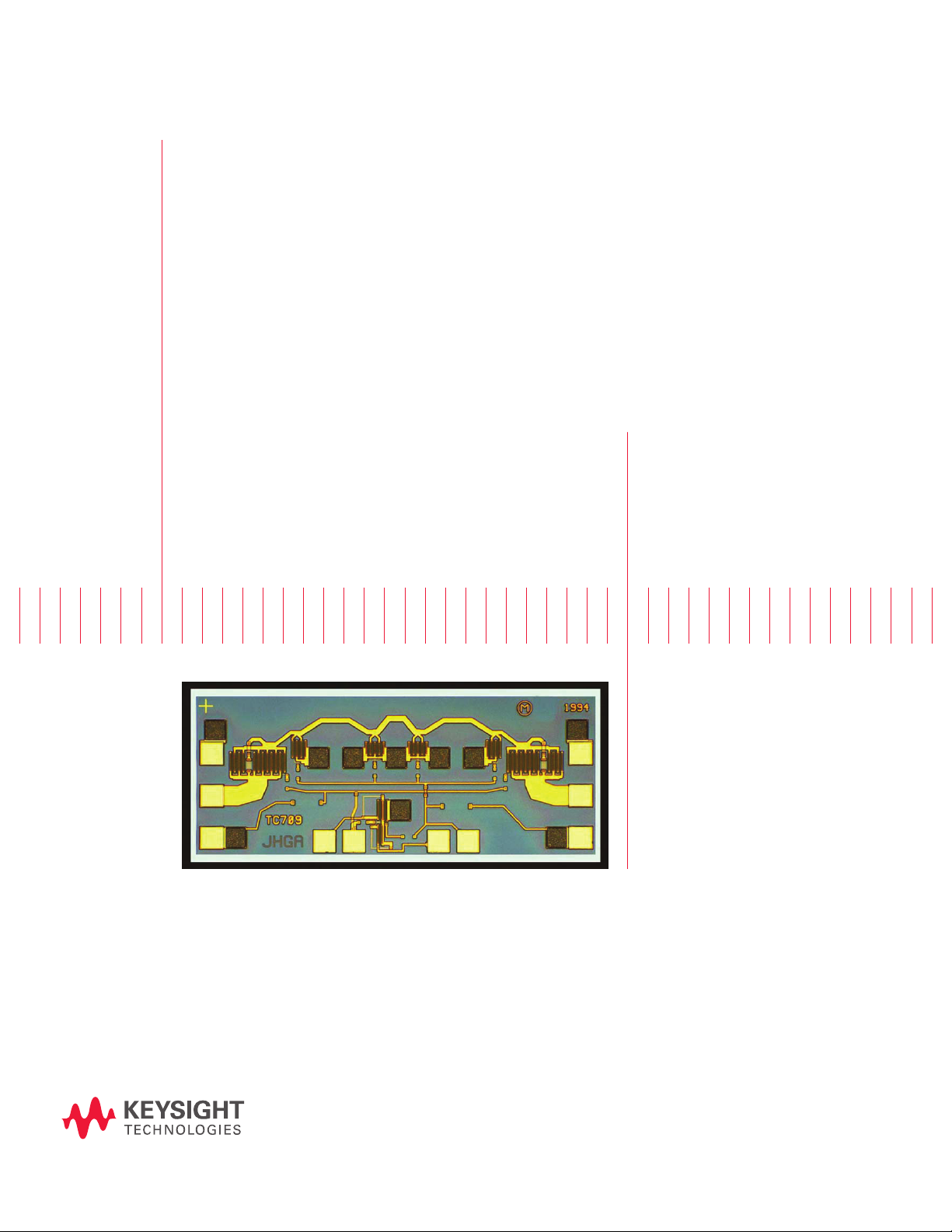
Keysight HMMC-1015
DC–50 GHz Variable Attenuator
1GG7-8008
Data Sheet
Features
– Specied frequency range:
DC to 26.5 GHz
– P
(–1 dB): 27 dBm @ 500 MHz
in
– Return loss: 10 dB
– Minimum attenuation: 2.0 dB
– Maximum attenuation: 30.0 dB
Page 2

02 | Keysight | HMMC-1015 DC–50 GHz Variable Attenuator - Data Sheet
Description
The HMMC-1015 is a monolithic, voltage variable, GaAs IC attenuator that operates
from DC to 50 GHz. The distributed topology of the HMMC-1015 minimizes the parasitic
effects of its series and shunt FETs, allowing the HMMC-1015 to exhibit a wide dynamic
range across its full bandwidth. An on-chip DC reference circuit may be used to maintain
optimum VSWR for any attenuation setting or to improve the attenuation versus voltage
linearity of the attenuator circuit.
Absolute Maximum Ratings1
Symbol Parameters/conditions Minimum Maximum Units
V
DC-RF
V
1
V
2
V
DC
P
in
T
mina
T
maxa
T
stg
T
max
DC voltage to RF ports –0.6 +1.6 Volts
V1 control voltage –10.5 +0.5 Volts
V2 control voltage –10.5 +0.5 Volts
DC in/DC out –0.6 +1.0 Volts
RF input power 17 dBm
Minimum ambient operating temperature –55 °C
Maximum ambient operating temperature +125 °C
Storage temperature –65 +165 °C
Maximum assembly temperature
+300 °C
(for 60 seconds maximum)
Chip size:
1470 x 610 µm (57.9 x 24.0 mils)
Chip size tolerance:
±10 µm (±0.4 mils)
Chip thickness:
127 ± 15 µm (5.0 ± 0.6 mils)
RF pad dimensions:
60 x 70 µm (2.4 x 2.8 mils) or larger
DC pad dimensions:
75 x 75 µm (3.0 x 3.0 mils) or larger
1. Operation in excess of any one of these conditions may result in permanent damage to this device
Page 3

03 | Keysight | HMMC-1015 DC–50 GHz Variable Attenuator - Data Sheet
DC Specications/Physical Properties
(TA = 25 °C)
Symbol Parameters/conditions Minimum Typical Maximum Units
I
V1
I
V2
V
p
V1 control current, (V1 = –10 V) 5.0 5.9 7.1 mA
V2 control current, (V2 = –10 V) 5.0 5.9 7.1 mA
Pinch-off voltage –6.75 –5.0 –3.75 Volts
Electrical Specications1
(TA = 25 °C, Z0 = 50 Ω)
Parameters/conditions Frequency (GHz) Minimum Typical Maximum Units
Minimum attenuation, |S21|
= 0 V, V2 = –10 V)
(V
1
Input/output return loss @
minimum attenuation setting,
= 0 V, V2 = –10 V)
(V
1
Maximum attenuation |S21|
(V
= –10 V, V2 = 0 V)
1
@ minimum attenuation 300 kHz
P
–1 dB
Input/output return loss @
maximum attention setting,
(V
= –0 V, V2 = 0 V)
1
DC power dissipation,
(V
= –10.5 V, V2 = –10.5 V)
1
(does not include input signals)
1.5 1.0 2.4 dB
8.0 1.4 2.4 dB
20.00 1.7 2.4 dB
26.5 2.0 2.4 dB
50.0 3.9 dB
< 26.5 10 16 dB
< 50.0 8 dB
1.5 27 30 dB
8.0 27 38 dB
20.0 27 38 dB
26.5 27 40 dB
50.0 35 dB
> 500 MHz
< 26.5
< 50.0
18.5
27
8 10
10
dBm
dBm
dB
dB
158 mW
1. Attenuation is a positive number; whereas, S21 as measured on a network analyzer would be a negative
number.
Page 4

04 | Keysight | HMMC-1015 DC–50 GHz Variable Attenuator - Data Sheet
Applications
The HMMC-1015 is designed to be used as a gain control block in an ALC assembly.
Because of its wide dynamic range and return loss performance, the HMMC-1015 may
also be used as a broadband pulse modulator or single-pole single-throw, non-reective
switch.
Operation
The attenuation value of the HMMC-1002 is adjusted by applying negative voltage
to V
. At any attenuation setting, optimum VSWR is obtained by applying negative
2
voltage to V
source-to-drain resistance and establishes the attenuation level. Applying negative
voltage (V
different attenuation settings. In some applications, a single setting of V
sufcient input and output match over the desired attenuation range (V
HMMC-1015 the values of V
voltage is monotonic for both V
and output return loss.
The attenuation and input/output match of the HMMC-1015 may also be controlled
using only a single input voltage by utilizing the on-chip DC reference circuit and the
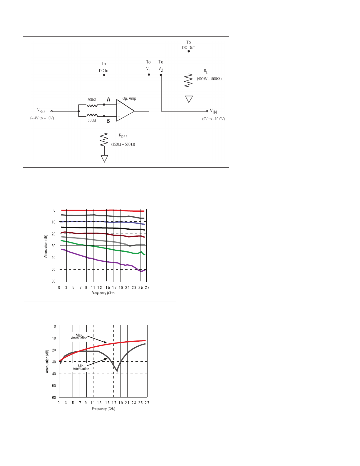
driver circuit shown in Figure 4. This circuit optimizes VSWR for any attenuation setting.
Because of process variations, the values of V
wafer if optimum performance is required. Typical values for these elements are given.
The ratio of the resistors R
voltage performance of the attenuator. For more information on the performance of
the HMMC-1015 and the driver circuits previously mentioned, see WPTC’s Application
Note, HMMC-1021 Attenuator: Attenuation Control, literature number 5991-3555EN. For
more S-parameter information, see WPTC’s Application Note, HMMC-1015 Attenuator:
S-Parameters, literature number 5991-3556EN.
. Applying negative voltage (V2) to the gates of the shunt FETs sets the
1
) to the gates of the series FETs optimizes the input and output match for
1
may be adjusted so that the device attenuation versus
1
and V2; however, this will slightly degrade the input
1
, R
REF
and R2 determines the sensitivity of the attenuation versus
1
, and RL are different for each
REF
may provide
1
). For any
2
Assembly Techniques
GaAs MMICs are ESD sensitive. ESD preventive measures must be employed in all aspects of storage, handling, and assembly.
MMIC ESD precautions, handling considerations, die attach and bonding methods are
critical factors in successful GaAs MMIC performance and reliability.
Keysight Technologies, Inc. application note, GaAs MMIC ESD, Die Attach and Bond-
ing Guidelines, literature number 5991-3484EN, provides basic information on these
subjects.
Page 5
05 | Keysight | HMMC-1015 DC–50 GHz Variable Attenuator - Data Sheet
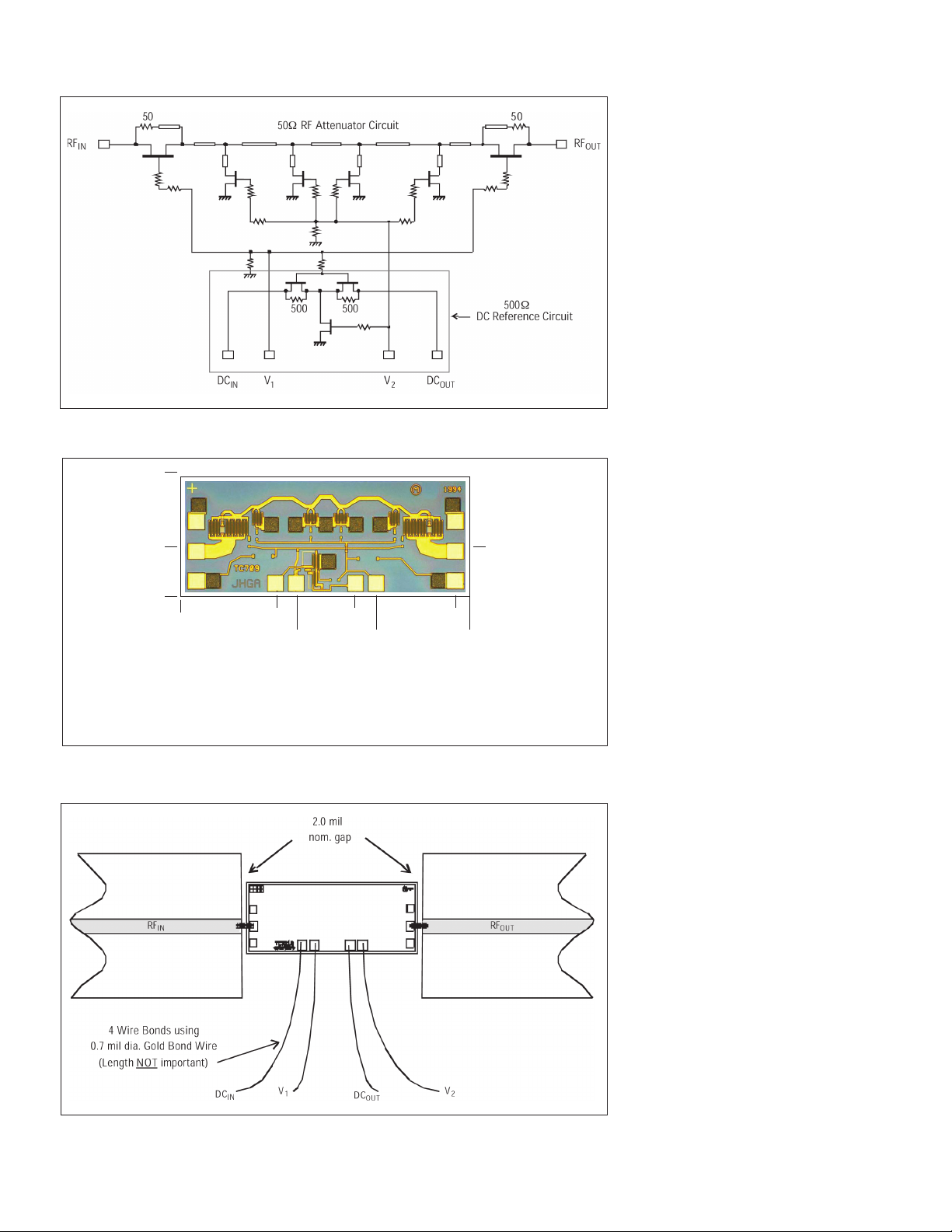
Figure 1. Schematic
610
RF
IN
RF
OUT
0
0
476
584
Notes:
1) All dimensions in microns and shown to center of bond pad.
2) DC
3) RF input and output bonding pads are 60 x 70 microns.
4) Chip thickness: 127 ± 15 µm.
, V1, DC
in
, and V2 bonding pads are 75 x 75 microns.
out
887
994 1470
1410
Figure 2. Bonding pad locations
233233
Figure 3. Assembly diagram
Page 6
06 | Keysight | HMMC-1015 DC–50 GHz Variable Attenuator - Data Sheet
Typical Performance
Figure 4. Attenuator driver
Figure 5. Attenuation vs. frequency
Figure 6. Output return loss vs. frequency
1
1
1. Data obtained from on-wafer measurements. T
chuck
= 25 °C.
Page 7
07 | Keysight | HMMC-1015 DC–50 GHz Variable Attenuator - Data Sheet
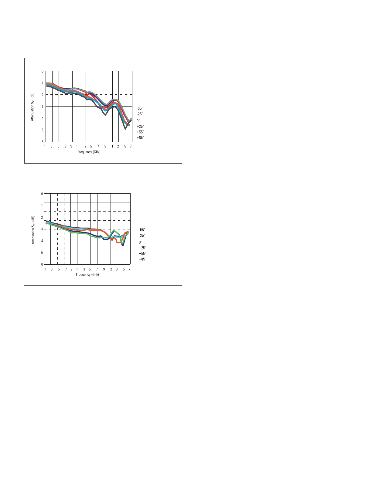
Typical Temperature Performance
Temperature setting
Temperature setting
Figure 7. Attenuation vs. temperature @ minimum at tenuation
Figure 8. Attenuation vs. temperature @ maximum attenuation
1
1
This data sheet contains a variety of typical and guaranteed performance data. The
information supplied should not be interpreted as a complete list of circuit specications. Customers considering the use of this, or other Keysight GaAs ICs, for their design
should obtain the current production specications from Keysight. In this data sheet the
term typical refers to the 50th percentile performance. For additional information contact Keysight [email protected].
1. Data taken with the device mounted in connectorized package
Page 8

08 | Keysight | HMMC-1015 DC–50 GHz Variable Attenuator - Data Sheet
myKeysight
www.keysight.com/find/mykeysight
A personalized view into the information most relevant to you.
www.axiestandard.org
AdvancedTCA® Extensions for Instrumentation and Test (AXIe) is an
open standard that extends the AdvancedTCA for general purpose and
semiconductor test. Keysight is a founding member of the AXIe consortium.
ATCA®, AdvancedTCA®, and the ATCA logo are registered US trademarks of
the PCI Industrial Computer Manufacturers Group.
www.lxistandard.org
LAN eXtensions for Instruments puts the power of Ethernet and the
Web inside your test systems. Keysight is a founding member of the LXI
consortium.
www.pxisa.org
PCI eXtensions for Instrumentation (PXI) modular instrumentation delivers a
rugged, PC-based high-performance measurement and automation system.
Three-Year Warranty
www.keysight.com/find/ThreeYearWarranty
Keysight’s commitment to superior product quality and lower total cost
of ownership. The only test and measurement company with three-year
warranty standard on all instruments, worldwide.
Keysight Assurance Plans
www.keysight.com/find/AssurancePlans
Up to five years of protection and no budgetary surprises to ensure your
instruments are operating to specification so you can rely on accurate
measurements.
www.keysight.com/quality
Keysight Technologies, Inc.
DEKRA Certified ISO 9001:2008
Quality Management System
Keysight Channel Partners
www.keysight.com/find/channelpartners
Get the best of both worlds: Keysight’s measurement expertise and product
breadth, combined with channel partner convenience.
For more information on Keysight
Technologies’ products, applications or
services, please contact your local Keysight
office. The complete list is available at:
www.keysight.com/find/contactus
Americas
Canada (877) 894 4414
Brazil 55 11 3351 7010
Mexico 001 800 254 2440
United States (800) 829 4444
Asia Pacic
Australia 1 800 629 485
China 800 810 0189
Hong Kong 800 938 693
India 1 800 112 929
Japan 0120 (421) 345
Korea 080 769 0800
Malaysia 1 800 888 848
Singapore 1 800 375 8100
Taiwan 0800 047 866
Other AP Countries (65) 6375 8100
Europe & Middle East
Austria 0800 001122
Belgium 0800 58580
Finland 0800 523252
France 0805 980333
Germany 0800 6270999
Ireland 1800 832700
Israel 1 809 343051
Italy 800 599100
Luxembourg +32 800 58580
Netherlands 0800 0233200
Russia 8800 5009286
Spain 0800 000154
Sweden 0200 882255
Switzerland 0800 805353
Opt. 1 (DE)
Opt. 2 (FR)
Opt. 3 (IT)
United Kingdom 0800 0260637
For other unlisted countries:
www.keysight.com/find/contactus
(BP-07-01-14)
This information is subject to change without notice.
© Keysight Technologies, 2013 - 2014
Published in USA, August 3, 2014
5989-6202EN
www.keysight.com
 Loading...