

KEXIN MOSFET Service Manual
SMD Type
MOSFET
MOS Field Effect Transistor
2SK3740
+0.1
Features
Gate voltage rating: 30 V
-0.1
1.27
Low on-state resistance
+0.2
R
DS(on) = 160 mÙ MAX. (VGS =10V,ID =10A)
-0.2
8.7
Low gate charge
+0.2
2.54
-0.2
5.28
+0.2
-0.2
Q
G =47nCTYP.(VDD = 200 V, VGS =10V,ID =20A)
Surface mount package available
Absolute Maximum Ratings Ta = 25
Parameter Symbol Rating Unit
Drain to source voltage V
Gate to source voltage V
Drain current
Power dissipation T
A=25
C=25
T
Channel temperature T
Storage temperature Tstg -55to+150
*PW 10 s,Duty Cycle 1%
DSS 250 V
GSS
D
I
dp *
I
P
D W
ch 150
30
20
60
1.5
100
1.27
+0.1
-0.1
5.08
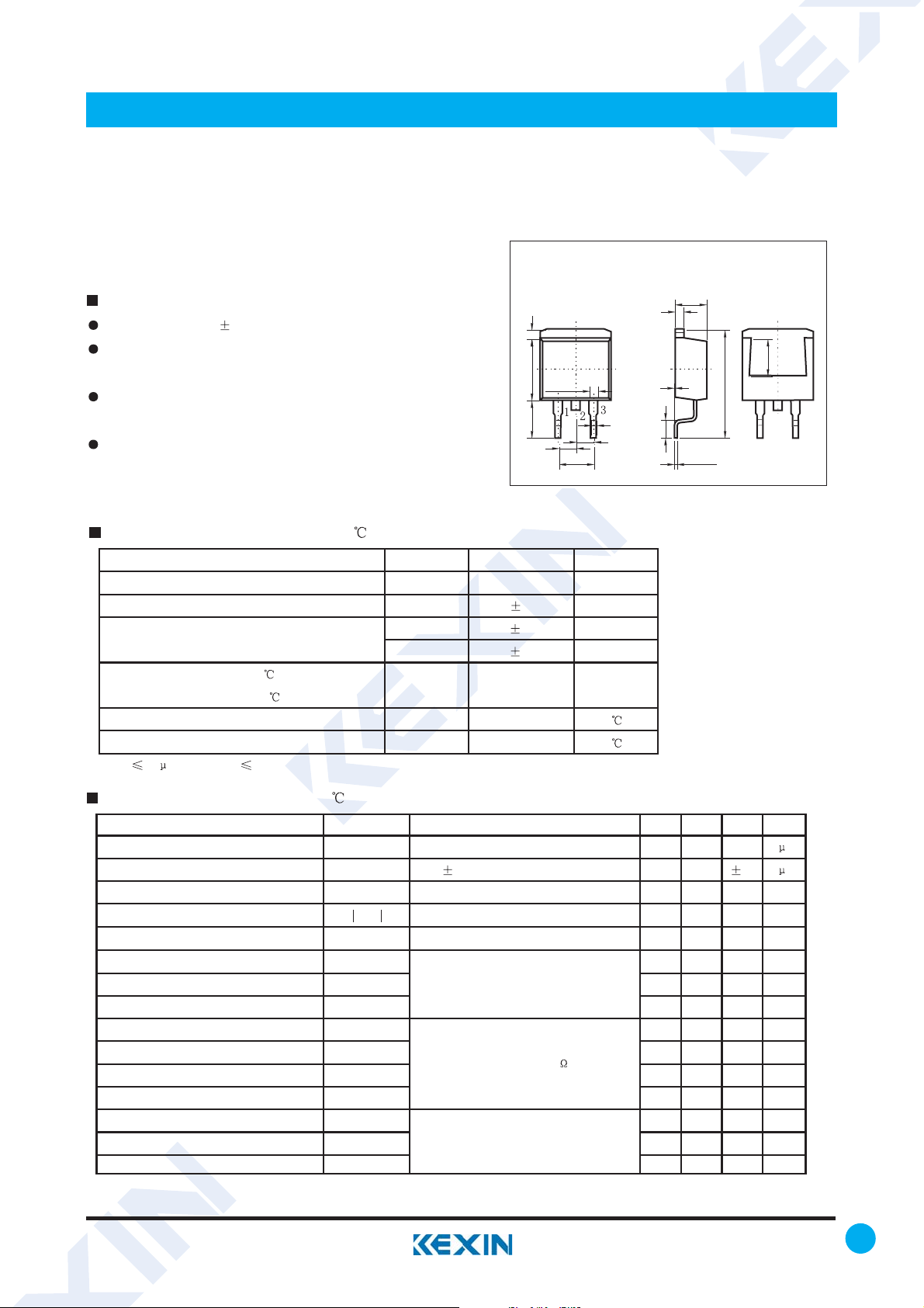
TO-263
0.81
2.54
+0.1
-0.1
V
Unit: mm
+0.2
4.57
-0.2
+0.1
1.27
-0.1
5.60
-0.2
15.25
1Gate
2Drain
3 Source
+0.1
-0.1
0.1max
+0.2
-0.2
2.54
0.4
+0.2
+0.2
-0.2
A
A
Electrical Characteristics Ta = 25
Parameter Symbol Testconditons Min Typ Max Unit
Drain cut-off current I
Gate leakage current I
Gate cut off voltage V
Forward transfer admittance
Drain to source on-state resistance R
Input capacitance C
Output capacitance C
Reverse transfer capacitance C
Turn-on delay time t
Rise time t
Turn-off delay time t
DSS VDS=250V,VGS=0 10
GSS
GS(off) VDS=10V,ID=1mA 2.5 3.5 4.5 V
Yfs
DS(on) VGS=10V,ID=10A 0.12 0.16 Ù
on 17 ns
off 49 ns
VGS= 30V,VDS=0 10 A
VDS=10V,ID=10A 7.0 15 S
iss 1720 pF
V
oss 330 pF
rss 170 pF
r 17 ns
DS=10V,VGS=0,f=1MHZ
D=10A,VGS(on)=10V,RG=0 ,VDD=125V
I
Fall time tf 9 ns
Total Gate Charge Q
Gate to Source Charge Q
Gate to Drain Charge Q
G 47 nC
GS 7nC
GD 25 nC
DD = 200V
V
GS =10V
V
I
D =20A
www.kexin.com.cn
A
1
 Loading...