

Kexin KI2302DS Schematic [ru]
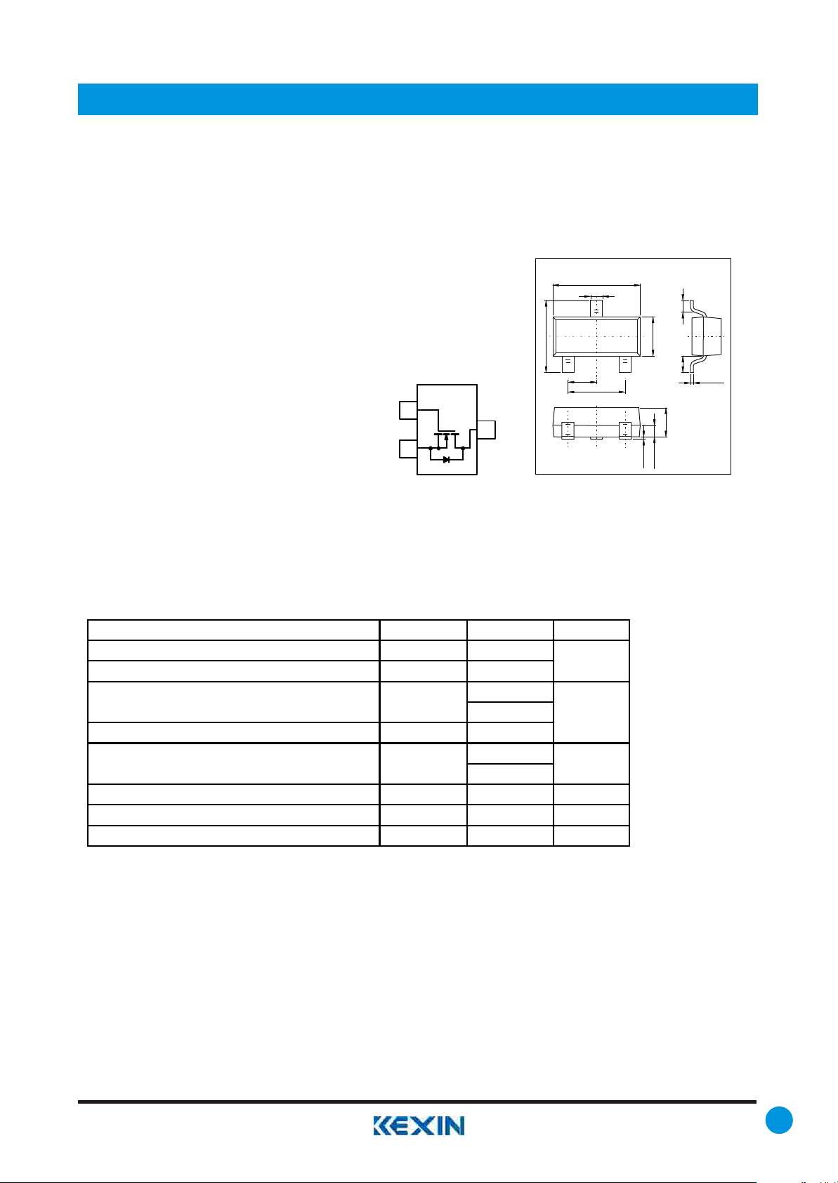
SMD Type
SMD Type
SMD Type
N-Channel MOSFET
KI2302DS
MOSFET
Diodes
MOSFET
■ Features
● VDS=20V
● RDS(on)= 0.085Ω@VGS=4.5V ,ID=3.6A
● RDS(on)= 0.115Ω@VGS=2.5V ,ID=
3.1A
1
G
3
S
2
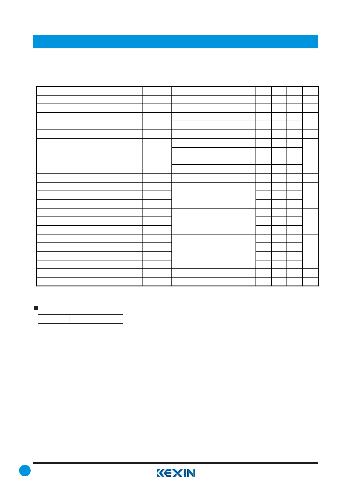
■ Absolute Maximum Ratings Ta = 25℃
Parameter Symbol Rating Unit
Drain-Source Voltage VDS 20
Gate-Source Voltage VGS
Continuous Drain Current Ta = 25℃
Ta=70℃
Pulsed Drain Current IDM 10
Power Dissipation Ta = 25℃
Ta=70℃
Thermal Resistance. Junction-to-Ambient RthJA 178
Junction Temperature TJ 150
Storage Temperature Tstg -55 to 150
ID
PD
0.46
D
±8
2.1
1.7
0.7
SOT-23
+0.1
-0.1
2.4
1 2
0.95
2.9
0.4
3
+0.1
-0.1
1.9
V
A
W
℃/W
℃
℃
+0.1
-0.1
+0.1
-0.1
+0.1
-0.1
0-0.1
Unit: mm
0.4
+0.1
-0.1
1.3
0.55
+0.05
0.1
-0.01
+0.1
-0.1
0.97
1.Base
1. Gate
2.Emitter
2. Source
+0.1
-0.1
3. Drain
3.collector
0.38
www.kexin.com.cn
1
Diodes
MOSFET
MOSFET
SMD Type
SMD Type
SMD Type
SMD Type
Diodes
KI2302DS
■ Electrical Characteristics Ta = 25℃
Parameter Symbol Testconditons Min Typ Max Unit
Drain-Source Breakdown Voltage VDSS VGS = 0 V, ID = 10 ìA 20 V
Gate-Threshold Voltage VGS(th)
Zero Gate Voltage Drain Current IDSS
Gate-Body Leakage IGSS
Drain-Source On-Resistance *
On-State Drain Current ID(on)
Forward Transconductance * gfs VDS = 5 V, ID = 3.6 A 8 S
Input Capacitance Ciss 300
Output Capacitance Coss 120
Reverse Transfer Capacitance Crss 80
Total Gate Charge Qg 4.0 10
Gate-Source Charge Qgs 0.65
Gate-Drain Charge Qgd 1.5
Turn-On Delay Time td(on) 7 15
Rise Time tr 55 80
Turn-Off Delay Time td(off) 16 60
Fall-Time tf 10 25
Continuous Source Current (Diode Conduction) IS 0.94 A
Diode Forward Voltage VSD IS = 0.94A, VGS = 0 V 0.76 1.2 V
*Pulse test: PW ≤300 ìs duty cycle≤2%..
rDS(on)
VDS = VGS, ID = 250 μA
VDS = 20 V, VGS = 0 V 1
VDS = 20 V, VGS = 0 V, TJ = 55℃
VDS = 0 V, VGS = ±8 V ±100
VGS = 4.5 V, ID = 3.6 A 0.045 0.085
VGS = 2.5 V, ID = 3.1 A 0.070 0.115
VDS ≥ 5 V, VGS = 4.5 V
VDS ≥ 5 V, VGS = 2.5 V
VDS=10V,VGS=0V,f=1MHz pF
VDS=10V,VGS=4.5V,ID=3.6A
VDD=10V,RL=5.5
≅
Ù,ID 3.6A,VGEN=4.5V,RG=6Ù
0.62 0.95 1.9
10
6
4
V
μA
nA
Ω
A
nC
ns
Marking
Marking A2SHB
2
www.kexin.com.cn
 Loading...