

Kexin KI2300 Schematics
SMD Type
SMD Type
N-Channel Enhancement Mode Field Effect Transistor
MOSFET
IC
KI2300(
SI2300)
Features
VDS=20V,RDS(ON)=40m @VGS=4.5V,ID=5.0A
VDS=20V,RDS(ON)=60m @VGS=2.5V,ID=4.0A
VDS=20V,,RDS(ON)=75m @VGS=1.8V,ID=1.0A
Absolute Maximum Ratings Ta = 25
Parameter Symbol Rating Unit
Drain-Source Voltage V
Gate-Source Voltage V
Drain-Current -Continuous * T
J=125
-Pulsed I
Power Dissipation * P
Thermal Resistance,Junction- to-Ambient R
Operating Junction and Storage Temperature Range Tj.Tstg -55 to 150
* Surface Mounted on FR 4 Board ,t 10 sec.
DS 20 V
GS
10
ID 3.8 A
DM 15 A
D 1.25 W
thJA 100
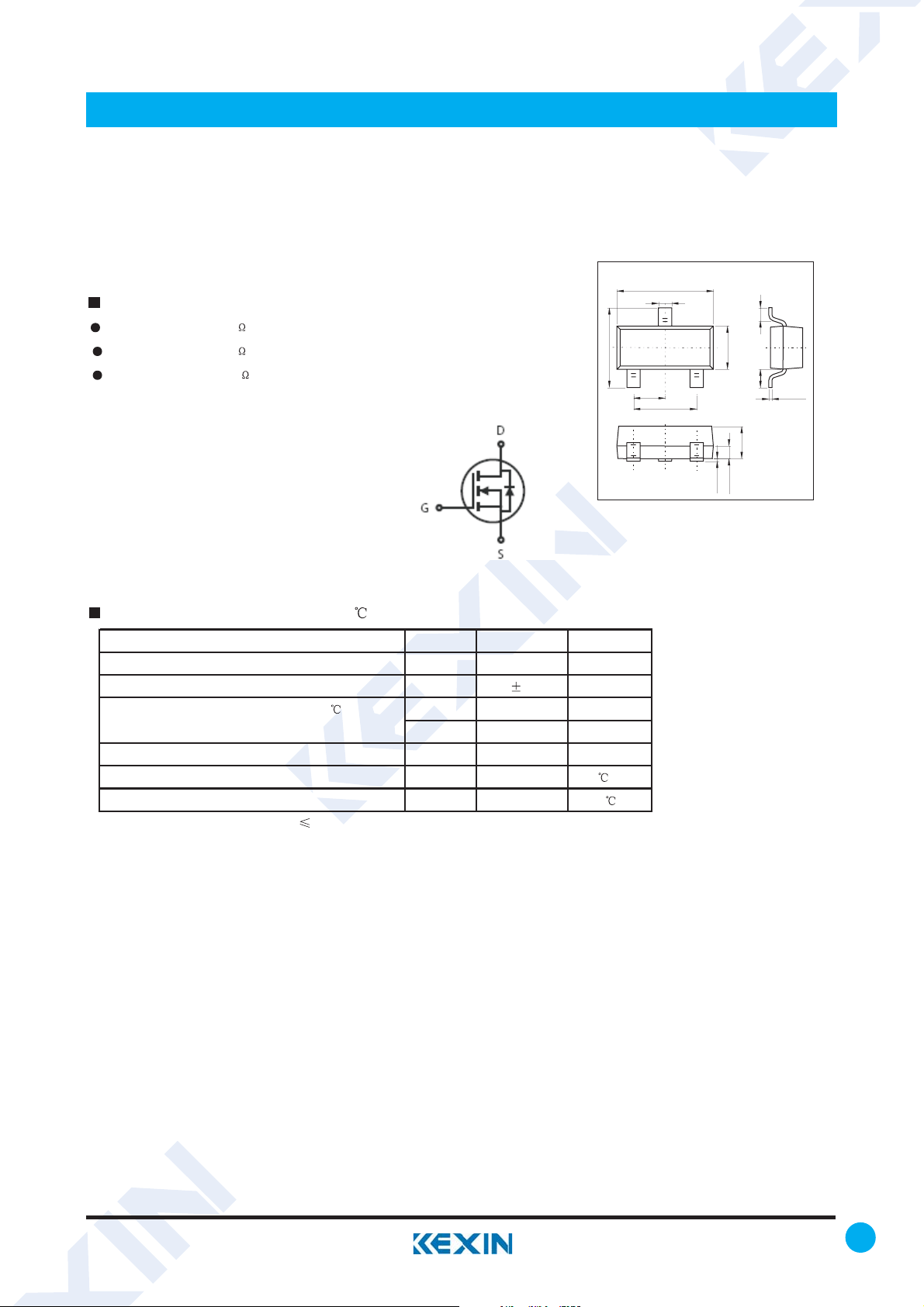
SOT-23
+0.1
2.9
-0.1
+0.1
0.4
-0.1
3
+0.1
-0.1
2.4
12
+0.1
0.95
-0.1
+0.1
1.9
-0.1
V
/W
0-0.1
Unit: mm
0.4
+0.1
-0.1
1.3
0.55
+0.05
0.1
-0.01
+0.1
-0.1
0.97
1.Base
1. Gate
2.Emitter
2. Source
+0.1
-0.1
3. Drain
3.collector
0.38
www.kexin.com.cn
1
SMD Type
SMD Type
MOSFET
KI2300(SI2300)
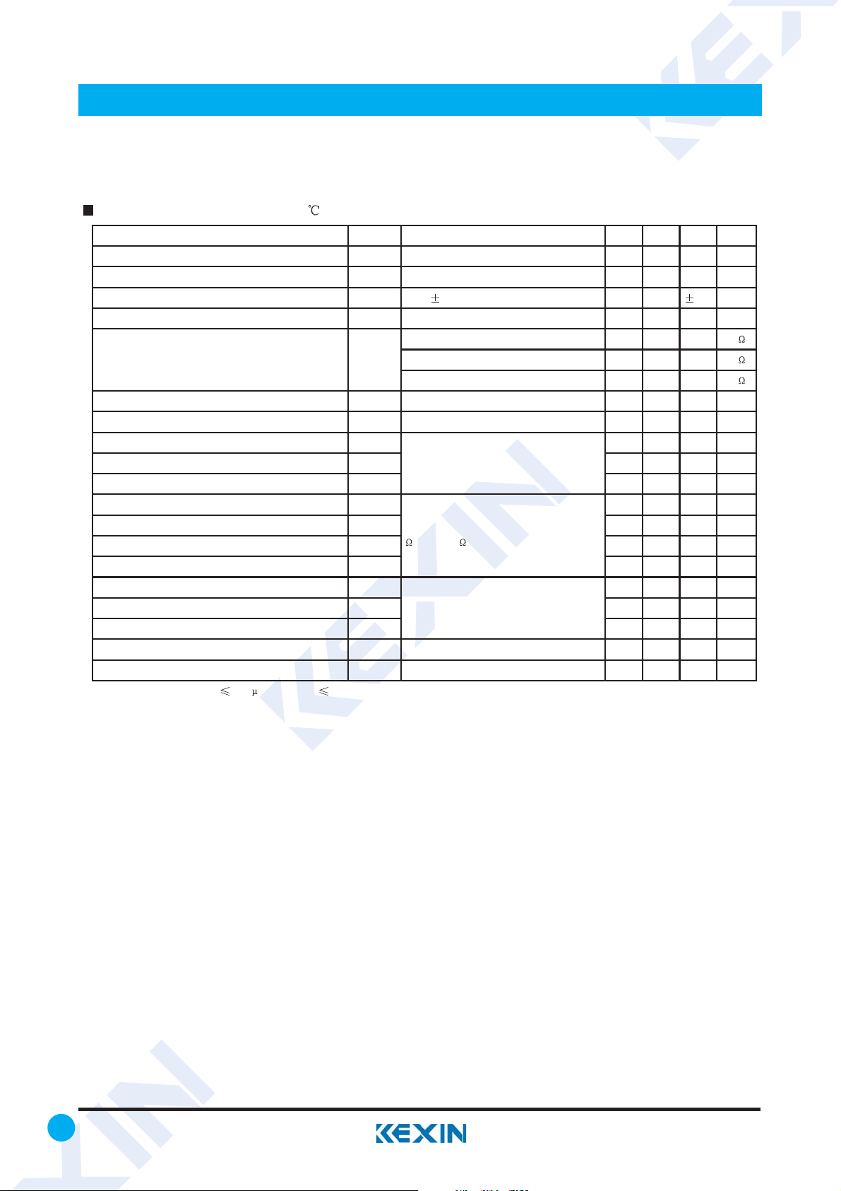
Electrical Characteristics Ta = 25
Parameter Symbol Testconditons Min Typ Max Unit
Drain-Source Breakdown Voltage V
Zero Gate Voltage Drain Current I
Gate-Body Leakage I
Gate Threshold Voltage * V
On-State Drain Current * ID(ON) VDS=5V,VGS=4.5V 18 A
Forward Transconductance * g
Input Capacitance C
Output Capacitance C
Reverse Transfer Capacitance C
Turn-On Delay Time t
Rise Time t
Turn-Off Delay Time t
Fall Time t
Total Gate Charge Q
Gate-S ource Charge Q
Gate-Drain Charge Q
Drain-Source Diode Forward Current * I
Diode Forward Voltage V
* Pulse Test:Pulse Width
300 ,Duty Cycle 2%
DSS VGS=0V,ID=250uA 20 V
DSS VDS=20V,V GS =0V 1 uA
GSS
VGS= 10V,VDS=0V 100
GS(th) VGS=VDS,ID=250uA 0.6 0.78 1.5 V
V
GS=4.5V,ID=5.0A 32 40
R
DS(ON)Drain- Source on-state Resistance *
VGS=2.5V,ID=4.0A 50 60
VGS=1.8V,ID=1.0A 62 75
FS VDS=5V,ID=5A 5 S
ISS 888 pF
VDS = 15V, VGS = 0V,f =1.0MHZ
OSS 144 pF
RSS 115 pF
D(on) 31.8 ns
r 14.5 ns
DD=10V,ID=1A,VGS=4.5V,RL=10
V
D(off) 50.3 ns
,RGEN=6
f 31.9 ns
g 16.8 nC
DS = 10V, ID =3.5A,VGS =4.5V
V
gs 2.5 nC
gd 5.4 nC
S 1.25 A
SD VGS=0V,IS=1.25A 0.825 1.2 V
IC
nA
m
m
m
2
www.kexin.com.cn
 Loading...