

Kexin BSS87 Schematics
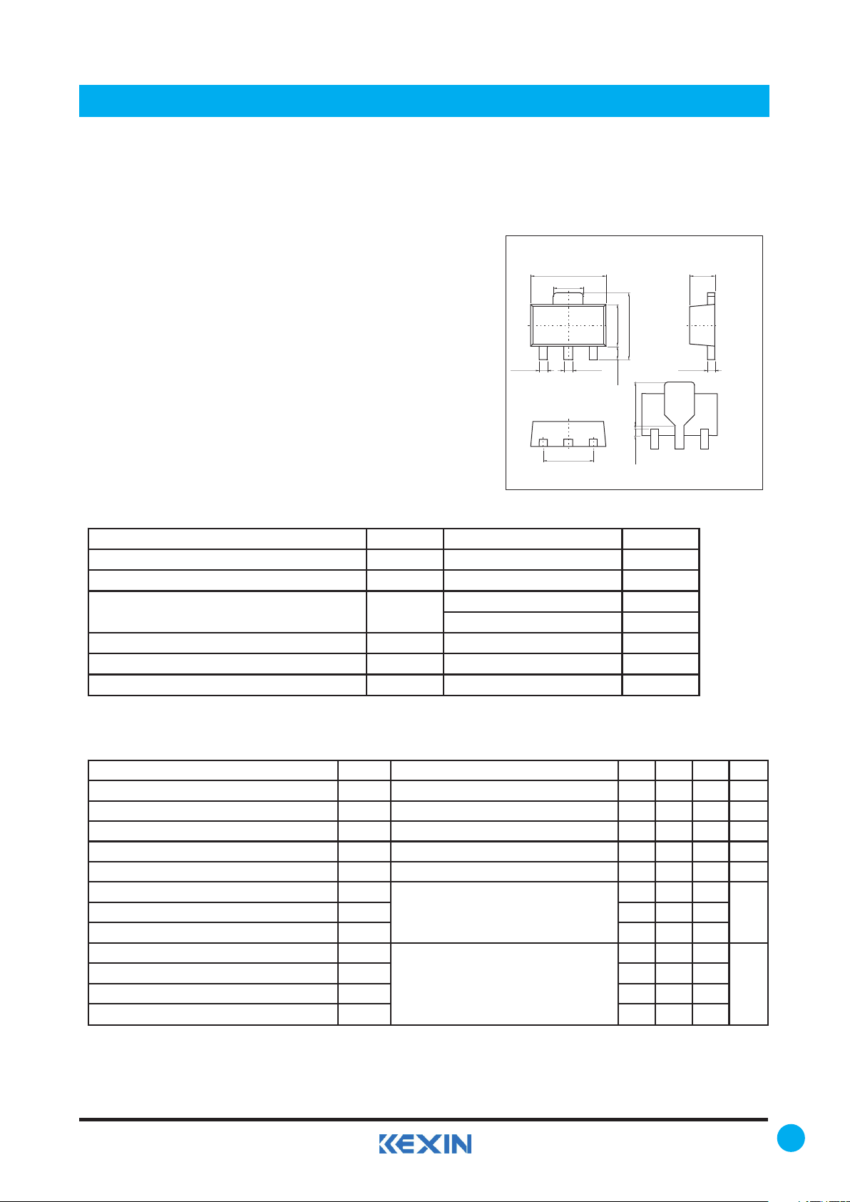
SMD Type
1.80
+0.1
-0.1
4.50
+0.1
-0.1
2.50
+0.1
-0.1
0.80
+0.1
-0.1
4.00
+0.1
-0.1
0.53
+0.1
-0.1
0.48
+0.1
-0.1
1.50
+0.1
-0.1
0.44
+0.1
-0.1
2.60
+0.1
-0.1
0.40
+0.1
-0.1
3.00
+0.1
-0.1
SOT-89
Unit: mm
1. Base
2. Collector
3. Emiitter
1. Source
2. Drain
3. Gate
123
1 Gate
2 Drain
3 Source
N-Channel Enhancement Mode MOSFET
BSS87
■ Features
● High-speed switching
● No secondary breakdown.
● Low RDS(on)
■ Absolute Maximum Ratings Ta = 25℃
Parameter Symbol Rating Unit
Drain-to-source voltage VDSS 200 V
Gate-to-source voltage VGS
±20
V
Drain Current – Continuous 280 mA
– Pulsed 1.1 A
Total power dissipation @ TA = 25℃
PD 1 W
Thermal resistance,junction-to-ambient RθJA 125
℃/W
Operating and storage temperature range TJ, Tstg -55 to 150
℃
ID
■ Electrical Characteristics Ta = 25℃
Parameter Symbol Test conditons Min Typ Max Unit
Drain-to-source breakdown voltage V(BR)DSS VGS = 0 V, ID = 250 μA 200 V
Zero Gate Voltage Drain Current IDSS VDS = 200 V, VGS = 0 60 μA
Gate-source leakage current IGSS
VGS = ± 20 V, VDS = 0 ±0.1
μA
Gate-source threshold voltage VGS(th) VDS = VGS, ID = 1.0 mA 0.8 2.8 V
Static drain-to-source on-rResistance RDS(on) VGS = 10V, ID = 400mA 6 Ω
Input capacitance Ciss 60
Output capacitance Coss 25
Transfer capacitance Crss 10
Turn-on delay time td(on) 10
Rise time tr 12
Turn-off delay time td(off) 25
Fall time
tf 40
VDS = 25 V, VGS = 0, f = 1 MHz
VDD = 120 V,VGS=10V, ID = 280m A,
RGEN = 6Ω
ns
pF
MOSFET
1
www.kexin.com.cn
1

 Loading...