

Page 1

OPERATOR MANUAL
KEPCO INC.
An ISO 9001 Company.
BIT 4886
DIGITAL INTERFACE CARD
WITH GPIB AND RS 232 CAPABILITY
MODEL
BIT 4886
INTERFACE CARD
IMPORTANT NOTES:
1) This manual is valid for the following Firmware Versions:
FIRMWARE VERSION NOTE.
2) A Change Page may be included at the end of the manual. All applicable changes and
revision number changes are documented with reference to the equipment serial numbers. Before using this Instruction Manual, check your equipment serial number to identify
your model. If in doubt, contact your nearest Kepco Representative, or the Kepco Documentation Office in New York, (718) 461-7000, requesting the correct revision for your
particular model and serial number.
3) The contents of this manual are protected by copyright. Reproduction of any part can be
made only with the specific written permission of Kepco, Inc.
Data subject to change without notice.
KEPCO®
©2013, KEPCO, INC
P/N 243-1303-r19
KEPCO, INC. ! 131-38 SANFORD AVENUE ! FLUSHING, NY. 11355 U.S.A. ! TEL (718) 461-7000 ! FAX (718) 767-1102
email: hq@kepcopower.com ! World Wide Web: http://www.kepcopower.com
THE POWER SUPPLIER™
Page 2

Page 3

TABLE OF CONTENTS
SECTION PAGE
SECTION 1 - INTRODUCTION
1.1 Scope of Manual ..................................................................................................................................... 1-1
1.2 General Description................................................................................................................................. 1-1
1.2.1 Measurements................................................................................................................................... 1-1
1.2.2 Enhanced Operation.......................................................................................................................... 1-2
1.3 Specifications .......................................................................................................................................... 1-2
1.3.1 BIT 4882 Compatibility....................................................................................................................... 1-4
SECTION 2 - INSTALLATION
2.1 Unpacking and Inspection ....................................................................................................................... 2-1
2.2 Set Start-up Defaults ............................................................................................................................... 2-1
2.2.1 Set (GPIB) Device Address ............................................................................................................... 2-2
2.2.2 Power Supply Identification ............................................................................................................... 2-2
2.3 Installation of Interface Card into the BOP .............................................................................................. 2-4
2.4 Input/Output Signals................................................................................................................................ 2-6
2.5 Initial Check-out Procedure ..................................................................................................................... 2-8
SECTION 3 - CALIBRATION
3.1 Equipment Required................................................................................................................................ 3-1
3.2 BOP Power Supply Adjustments............................................................................................................. 3-1
3.2.1 Adjustment of the Bop ±10 Volt Calibration Controls (R31, R32) ...................................................... 3-1
3.2.2 Adjustment of the Ammeter Zero (R50)............................................................................................. 3-1
3.3 Calibration of BIT 4886 Interface Card .................................................................................................... 3-3
3.3.1 Manual calibration.............................................................................................................................. 3-6
3.3.2 Calibration of BIT 4886 Interface Card using the VISA Driver Soft Panel ......................................... 3-9
3.3.2.1 Calibration Basics ........................................................................................................................ 3-10
3.3.2.2 Calibration Procedure .................................................................................................................. 3-11
SECTION 4 - OPERATION
4.1 General.................................................................................................................................................... 4-1
4.1.1 Programming Techniques to Optimize Power Supply performance .................................................. 4-1
4.1.1.1 Setting BOP Voltage and Current Limits...................................................................................... 4-1
4.1.1.2 Automatic Range Operation......................................................................................................... 4-2
4.1.1.3 Using the BIT 4886 to Produce a Software-timed Ramp at the BOP Output............................... 4-2
4.1.2 Making Sure the Previous Command is Complete ............................................................................ 4-2
4.2 Initialization of the BIT 4886 Card ........................................................................................................... 4-4
4.2.1 Initialization using CVI Driver - GPIB Port Only................................................................................. 4-4
4.2.2 Initialization using SCPI Commands and GPIB Port ......................................................................... 4-6
4.2.3 Initialization using SCPI Commands and RS 232 Port ...................................................................... 4-7
4.2.4 Password Setup................................................................................................................................. 4-7
4.2.4.1 Forgotten Passwords................................................................................................................... 4-7
4.3 Built in Test.............................................................................................................................................. 4-8
4.3.1 Power-up Test ................................................................................................................................... 4-8
4.3.2 Confidence Test................................................................................................................................. 4-8
4.3.3 BOP test ............................................................................................................................................ 4-9
4.4 IEEE 488 (GPIB) Bus Protocol................................................................................................................ 4-9
4.5 RS232-C Operation................................................................................................................................. 4-10
4.5.1 Serial INterface.................................................................................................................................. 4-11
4.5.2 RS 232 Implementation ..................................................................................................................... 4-11
4.5.2.1 Echo Mode................................................................................................................................... 4-13
4.5.2.2 XON XOFF Method...................................................................................................................... 4-13
4.5.2.3 Isolating RS 232 Communication Problems ................................................................................ 4-13
4.5.3 Using SCPI commands for RS 232 Communication. ........................................................................ 4-14
4.6 SCPI Programming ................................................................................................................................. 4-14
4.6.1 SCPI Messages ................................................................................................................................. 4-14
4.6.2 Common Commands/Queries ........................................................................................................... 4-14
BIT 4886120413 i
Page 4

TABLE OF CONTENTS
SECTION PAGE
4.6.3 SCPI Subsystem Command/Query Structure................................................................................... 4-14
4.6.3.1 Initiate Subsystem....................................................................................................................... 4-15
4.6.3.2 Measure Subsystem ................................................................................................................... 4-15
4.6.3.3 [Source:]voltage And [Source:]current Subsystems.................................................................... 4-16
4.6.3.4 Output Subsystem....................................................................................................................... 4-16
4.6.3.5 List Subsystem............................................................................................................................ 4-16
4.6.3.5.1 Required LIST Commands..................................................................................................... 4-16
4.6.3.5.2 Other Required Commands ................................................................................................... 4-17
4.6.3.5.3 Other Useful Commands........................................................................................................ 4-17
4.6.3.5.4 Optional Commands............................................................................................................... 4-17
4.6.3.6 Status Subsystem ....................................................................................................................... 4-17
4.6.3.7 System Subsystem ..................................................................................................................... 4-17
4.6.4 Program Message Structure............................................................................................................. 4-17
4.6.4.1 Keyword ...................................................................................................................................... 4-18
4.6.4.2 Keyword Separator ..................................................................................................................... 4-19
4.6.4.3 Query Indicator............................................................................................................................ 4-19
4.6.4.4 Data............................................................................................................................................. 4-19
4.6.4.5 Data Separator............................................................................................................................ 4-19
4.6.4.6 Message Unit Separator ............................................................................................................. 4-19
4.6.4.7 Root Specifier.............................................................................................................................. 4-19
4.6.4.8 Message Terminator ................................................................................................................... 4-19
4.6.5 Understanding The Command Structure .......................................................................................... 4-20
4.6.6 Program Message Syntax Summary ................................................................................................ 4-20
4.6.7 SCPI Program Example.................................................................................................................... 4-21
4.7 Enhanced Operation............................................................................................................................... 4-21
4.7.1 Error Detection.................................................................................................................................. 4-22
4.7.2 Limit Channel Control ....................................................................................................................... 4-22
4.7.3 Using and Saving System Variables................................................................................................. 4-23
4.7.4 Flash Memory EEPROM Operation.................................................................................................. 4-23
4.7.4.1 Calibration Storage ..................................................................................................................... 4-26
APPENDIX A - SCPI COMMON COMMAND/QUERY DEFINITIONS
A-1 Introduction............................................................................................................................................. A-1
A.2 *CLS — Clear Status Command .......................................................................................................... A-1
A.3 *ESE — Standard Event Status Enable Command................................................................................ A-1
A.4 *ESE? — Standard Event Status Enable Query..................................................................................... A-2
A.5 *ESR? — Event Status Register Query................................................................................................. A-2
A.6 *IDN? — Identification Query.................................................................................................................. A-2
A.7 *OPC — Operation Complete Command ............................................................................................... A-3
A.8 *OPT? — Options Query ........................................................................................................................ A-4
A.9 *RCL — Recall Command ...................................................................................................................... A-4
A.10 *RST — Reset Command....................................................................................................................... A-4
A.11 * SAV — Save Command...................................................................................................................... A-4
A.12 *SRE — Service Request Enable Command ......................................................................................... A-4
A.13 *SRE? — Service Request Enable Query .............................................................................................. A-5
A.14 *STB? — Status Byte Register Query .................................................................................................... A-5
A.15 *TRG — Trigger Command .................................................................................................................... A-5
A.16 *TST? — Self Test Query....................................................................................................................... A-5
A.17 *WAI — Wait-To-Continue Command .................................................................................................... A-5
ii BIT 4886120413
Page 5

TABLE OF CONTENTS
SECTION PAGE
APPENDIX B - SCPI COMMAND/QUERY DEFINITIONS
B.1 Introduction............................................................................................................................................. B-1
B.2 Numerical Values ................................................................................................................................... B-2
B.3 CALibrate:CPRotect Command ............................................................................................................. B-2
B.4 CALibrate:STATus Command ................................................................................................................ B-2
B.5 CALibrate[:STATus]? Query................................................................................................................... B-2
B.6 CALibrate:CURRent Command ............................................................................................................. B-3
B.7 CALibrate:DATA Command ................................................................................................................... B-3
B.8 CALibrate:DPOT Command ................................................................................................................... B-3
B.9 CALibrate:LCURR Command ................................................................................................................ B-4
B.10 CALibrate:LVOLT Command ................................................................................................................. B-4
B.11 CALibrate:SAVE Command ................................................................................................................... B-4
B.12 CALibrate:VOLTage Command ............................................................................................................. B-4
B.13 CALibrate:VPRotect Command.............................................................................................................. B-4
B.14 CALibrate:ZERO Command................................................................................................................... B-4
B.15 INITiate[:IMMediate] Command ............................................................................................................. B-5
B.16 INITiate:CONTinuous Command ........................................................................................................... B-5
B.17 INITiate:CONTinuous Query .................................................................................................................. B-5
B.18 MEASure[:SCALar]:CURRent[:DC]?
B.19 MEASure[:VOLTage][:SCALar][:DC]? Query......................................................................................... B-5
B.20 OUTPut[:STATe] Command................................................................................................................... B-5
B.21 OUTPut[:STATe] Query ......................................................................................................................... B-5
B.22 [SOURce:]FUNCtion:MODE Command ................................................................................................. B-6
B.23 [SOURce:]FUNCtion:MODE? Query ...................................................................................................... B-6
B.24 [SOURce:]FUNCtion:MODE:TRIGger .................................................................................................... B-6
B.25 [SOURce:]FUNCtion:MODE:TRIGger? Query ....................................................................................... B-6
B.26 [SOURce:]LIST:CLEar Command.......................................................................................................... B-6
B.27 [SOURce:]LIST:COUNt Command......................................................................................................... B-6
B.28 [SOURce:]LIST:COUNt? Query ............................................................................................................. B-6
B.29 [SOURce:]LIST:COUNt:SKIP Command ............................................................................................... B-7
B.30 [SOURce:]LIST:COUNt:SKIP? Query.................................................................................................... B-7
B.31 [SOURce:]LIST:CURRent Command..................................................................................................... B-7
B.32 [SOURce:]LIST:CURRent? Query ......................................................................................................... B-7
B.33 [SOURce:]LIST:CURRent:POINts? Query............................................................................................. B-7
B.34 [SOURce:]LIST:DIRection Command .................................................................................................... B-8
B.35
B.36 [SOURce:]LIST:DWELl Command......................................................................................................... B-8
B.37 [SOURce:]LIST:DWELl? Query.............................................................................................................. B-8
B.38 [SOURce:]LIST:DWELl:POINts? Query................................................................................................. B-8
B.39 [SOURce:]LIST:GENeration Command ................................................................................................. B-12
B.40 [SOURce:]LIST:GENeration? Query ...................................................................................................... B-12
B.41 [SOURce:]LIST:QUERy Command........................................................................................................ B-12
B.42 [SOURce:]LIST:QUERy? Query............................................................................................................. B-12
B.43 [SOURce:]LIST:SEQuence Command................................................................................................... B-12
B.44 [SOURce:]LIST:SEQuence? Query ....................................................................................................... B-12
B.45 [SOURce:]LIST:VOLTage Command..................................................................................................... B-13
B.46 [SOURce:]LIST:VOLTage? Query ......................................................................................................... B-13
B.47 [SOURce:]LIST:VOLTage:POINts? Query............................................................................................. B-13
B.48 [SOURce:]CURRent[:LEVel][:IMMediate][:AMPlitude] Command.......................................................... B-13
B.49 [SOURce:]CURRent[:LEVel][:IMMediate][:AMPlitude] Query ................................................................ B-13
B.50 [SOURce:]CURRent:MODe Command .................................................................................................. B-14
B.51 [SOURce:]CURRent:MODE?
B.52 [SOURce:]CURRent:[:LEVel]RANGe Command ................................................................................... B-15
B.53 [SOURce:]CURRent:[:LEVel]RANGe? Query ........................................................................................ B-15
B.54 [SOURce:]CURRent:[:LEVel]RANGe:AUTO Command ........................................................................ B-15
[SOURce:]LIST:DIRection? Query......................................................................................................... B-8
Query ........................................................................................... B-5
Query..................................................................................................... B-15
BIT 4886120413 iii
Page 6

TABLE OF CONTENTS
SECTION PAGE
B.55 [SOURce:]CURRent[:LEVel]TRIGgered[:AMPlitude] Command............................................................ B-15
B.56 [SOURce:]CURRent[:LEVel]TRIGgered[:AMPlitude]? Query................................................................. B-15
B.57 [SOURce:]VOLTage[:LEVel][:IMMediate][:AMPlitude] Command.......................................................... B-16
B.58 [SOURce:]VOLTage[:LEVel][:IMMediate][:AMPlitude]? Query............................................................... B-16
B.59 [SOURce:]VOLTage:MODE Command.................................................................................................. B-16
B.60 [SOURce:]VOLTage:MODE? Query....................................................................................................... B-17
B.61 [SOURce:]VOLTage[:LEVel]:RANGe Command.................................................................................... B-17
B.62 [SOURce:]VOLTage:[:LEVel]RANGe? Query ........................................................................................ B-17
B.63 [SOURce:]VOLTage:[:LEVel]RANGe:AUTO Command......................................................................... B-17
B.64 [SOURce:]VOLTage[:LEVel]:TRIGgered[:AMPlitude] Command........................................................... B-17
B.65 [SOURce:]VOLTage:[:LEVel]:TRIGgered[:AMPlitude]? Query............................................................... B-18
B.66 STATus:OPERation:CONDition Query................................................................................................... B-18
B.67 STATus:OPERation:ENABle Command................................................................................................. B-18
B.68 STATus:OPERation:ENABle? Query ..................................................................................................... B-18
B.69 STATus:OPERation[:EVENt]? Query ..................................................................................................... B-18
B.70 STATus:PRESet Command ................................................................................................................... B-18
B.71 STATus:QUEStionable[:EVENt]? Query ................................................................................................ B-19
B.72 STATus:QUEStionable:CONDition? Query ............................................................................................ B-20
B.73 STATus:QUEStionable:ENABle Command............................................................................................ B-20
B.74 STATus:QUEStionable:ENABle? Query................................................................................................. B-20
B.75 SYSTem:BEEP Command ..................................................................................................................... B-20
B.76 SYSTem:COMMunication:SERial:ECHO
B.77 SYSTem:COMMunication:SERial:ECHO? Query .................................................................................. B-20
B.78 SYSTem:COMMunication:SERial:PACE
B.79 SYSTem:COMMunication:SERial:PACE? Query ................................................................................... B-20
B.80 SYSTem:ERRor? Query......................................................................................................................... B-21
B.81 SYSTem:ERRor:CODE? Query ............................................................................................................. B-21
B.82 SYSTem:ERRor:CODE:ALL? Query ...................................................................................................... B-21
B.83 SYSTem:PASSword:CENable Command.............................................................................................. B-21
B.84 SYSTem:PASSword:CDISable Command............................................................................................. B-21
B.85 SYSTem:PASSword:NEW Command.................................................................................................... B-21
B.86 SYSTem:PASSword:STATe? Query ...................................................................................................... B-21
B.87 SYSTem:REMote
B.88 SYSTem:REMote? Query....................................................................................................................... B-21
B.89 SYSTem:SECurity:IMMediate Command............................................................................................... B-22
B.90 SYSTem:SET Command........................................................................................................................ B-23
B.91 SYSTem:SET? Query............................................................................................................................. B-23
B.92 SYSTem:VERSion? Query ..................................................................................................................... B-23
Command ................................................................................................................ B-21
Command ............................................................................ B-20
Command............................................................................. B-20
iv BIT 4886120413
Page 7

LIST OF FIGURES
FIGURE TITLE PAGE
1-1 Remotely Controlled Power Supply Configurations Using Kepco Products................................................ viii
2-1 BIT 4886 Switch Locations ......................................................................................................................... 2-2
2-2 Installation of Model BIT 4886 into BOP ..................................................................................................... 2-5
2-3 IEEE 488 (GPIB) Connector ....................................................................................................................... 2-6
2-4 RJ45 to DB9 Adapter Wiring....................................................................................................................... 2-7
3-1 BOP Power Supply, Internal Calibration Control Locations ........................................................................ 3-2
3-2 Current Shunt Connections......................................................................................................................... 3-2
3-3 Main Panel .................................................................................................................................................. 3-9
3-4 Calibration Panel......................................................................................................................................... 3-10
4-1 Programming Example to Verify Previous Command has Completed........................................................ 4-4
4-2 VISA Driver Start-up ................................................................................................................................... 4-5
4-3 BIT 4886 Card Initialization using VISA Driver............................................................................................ 4-6
4-4 RS 232 Implementation .............................................................................................................................. 4-12
4-5 Tree Diagram of SCPI Commands Used with BIT 4886 Interface Card ..................................................... 4-15
4-6 Message Structure...................................................................................................................................... 4-18
4-7 Typical Example of Interface Card Program Using SCPI Commands ........................................................ 4-22
A-1 GPIB Commands ....................................................................................................................................... A-3
B-1 Using Calibration Commands and Queries................................................................................................ B-3
B-2 Using LIST Commands for Sawtooth and Triangle Waveforms................................................................. B-9
B-3 Using LIST Commands and Queries ......................................................................................................... B-10
B-4 Programming the Output............................................................................................................................ B-14
B-5 Using Recall and Trigger Functions ........................................................................................................... B-16
B-6 Using Status Commands and Queries....................................................................................................... B-19
B-7 Setting the Unit to Remote Mode via Serial (RS 232) Port ........................................................................ B-22
B-8 Using System Commands and Queries..................................................................................................... B-23
BIT 4886120413
v
Page 8

LIST OF TABLES
TABLE TITLE PAGE
1-1 Applicability of BIT 4886 Cards to Specific BOP Models ........................................................................... 1-1
1-2 BOP Voltage Specifications with BIT 4886 Installed .................................................................................. 1-2
1-3 BOP Current Specifications with BIT 4886 Installed .................................................................................. 1-2
1-4 Specifications, BIT 4886 ............................................................................................................................. 1-3
1-5 Command Differences for BIT 4886 card Configured as BIT 4882 ............................................................ 1-4
2-1 Items Supplied ............................................................................................................................................ 2-1
2-2 Device Address Selection .......................................................................................................................... 2-3
2-3 Input/Output Pin Assignments .................................................................................................................... 2-6
2-4 RS232C PORT Input/Output Pin Assignments .......................................................................................... 2-7
2-5 RJ45 to DB9 Adapter Wire Functions ........................................................................................................ 2-7
3-1 Calibration Measurements and Tolerances - Voltage ................................................................................ 3-3
3-2 Calibration Measurements and Tolerances - Current ................................................................................ 3-4
3-3 Suggested Sense Resistors ....................................................................................................................... 3-5
3-4 Calibration Panel Functions ....................................................................................................................... 3-10
4-1 Built-in test Error Codes ............................................................................................................................. 4-8
4-2 IEEE 488 (GPIB) Bus Interface Functions ................................................................................................. 4-9
4-3 IEEE 488 (GPIB) Bus Command Mode Messages .................................................................................... 4-10
4-4 IEEE 488 (GPIB) Bus Data Mode Messages ............................................................................................. 4-11
4-5 Enhanced Operation - Error Response ...................................................................................................... 4-24
4-6 Calibration Storage ..................................................................................................................................... 4-27
A-1 IEEE 488.2 Command/query Index ............................................................................................................A-1
A-2 Standard Event Status Enable Register and Standard Event Status Register Bits ...................................A-1
A-3 Service Request Enable and Status Byte Register Bits .............................................................................A-5
B-1 SCPI Subsystem Command/query Index ...................................................................................................B-1
B-2 List Data Table ...........................................................................................................................................B-7
B-3 List Sequence Table ...................................................................................................................................B-12
B-4 Operation Condition Register, Operation Enable Register,
and Operation Event Register Bits ..........................................................................................................B-18
B-5 Questionable Event Register, Questionable Condition Register
and Questionable Condition Enable Register Bits ...................................................................................B-19
B-6 Error Messages ..........................................................................................................................................B-22
vi BIT 488612413
Page 9

Page 10

(vii Blank)/viii BIT4886 120413
FIGURE 1-1. REMOTELY CONTROLLED POWER SUPPLY CONFIGURATIONS USING KEPCO PRODUCTS
Page 11

1.1 SCOPE OF MANUAL
This manual contains instructions for the installation, operation and maintenance of the BIT
4886 Interface Card manufactured by Kepco, Inc, Flushing, NY, U.S.A.
1.2 GENERAL DESCRIPTION
The Kepco BIT Card Series were designed as an accessory for the Kepco BOP series bipolar
power supplies. The BIT 4886 card makes it possible to control the BOP output by means of
digital input signals via the IEEE 488.2 bus using SCPI commands (see Figure 1-1). The BIT
4886 card acts as an interface between the digital data bus and the BOP, accepting the digital
input data and converting it to an analog signal, which in turn, controls the BOP output. The BIT
4886 provides full talk/listen capability and is fully compliant with the SCPI programming language.
At power-up the BIT 4886 is set to local mode, allowing front panel control of the BOP power
Supply. Upon power up the BIT 4886 performs a reset, establishing the voltage and current output levels to be 0 volts and the output state to be off.
The BIT 4886 is a 16-bit interface card which allows either plus or minus voltage or current output at 15 bits of resolution.
SECTION 1 - INTRODUCTION
Table 1-1 shows which specific revisions of BOP models are compatible with BIT 4886 cards.
TABLE 1-1. APPLICABILITY OF BIT 4886 CARDS TO SPECIFIC BOP MODELS
MODEL REVISION NO. MODEL REVISION NO.
BOP 20-5M 2 AND LATER BOP 50-8M 10 AND LATER
BOP 20-10M 17 AND LATER BOP 72 3M 10 AND LATER
BOP 20-20M 15 AND LATER BOP 72-6M 14 AND LATER
BOP 36-6M 19 AND LATER BOP 100-1M 24 AND LATER
BOP 36-12M 13 AND LATER BOP 100-2M 15 AND LATER
BOP 50-2M 21 AND LATER BOP 100-4M 14 AND LATER
BOP 50-4M 13 AND LATER BOP 200-1M 7 AND LATER
NOTE: For modification (to accept the BIT 4886 card) of BOP Models with revision numbers that
do not appear in this table, contact Kepco for assistance.
1.2.1 MEASUREMENTS
The readback information for BIT 4886 cards is the average of the last 16 measurements. The
measurement average is valid after a time delay which allows the readings to stabilize, plus 320
milliseconds.
BIT 4886 OPR 120413 1-1
Page 12

1.2.2 ENHANCED OPERATION
The BIT 4886 card includes the following enhanced operation features: a) advanced control
over the way the unit responds to errors (PAR. 4.7.1), b) advanced limit channel control for
applications such as battery, photocell, and large inductor applications (see PAR. 4.7.2) and c)
ability to save system settings (PAR. 4.7.3).
1.3 SPECIFICATIONS
For voltage and current accuracy specifications of BOP Models with a BIT 4886 card installed,
refer to Tables 1-2 and 1-3, respectively. Table 1-4 lists the specifications for the BIT 4886 card.
TABLE 1-2. BOP VOLTAGE SPECIFICATIONS WITH BIT 4886 INSTALLED
VOLTAGE
SPECIFICATION
High range accuracy 24mV 12mV 8mV 6mV 4mV 2.4mV
Low Range Accuracy
Positive Limit Accuracy
Measurement Accuracy 120mV 60mV 45mV 30mV 24mV 12mV
NOTES:1. Low range is defined as less than 1/4 of the rated value.
2. Positive limit accuracy applies to limit values from nominal to 2% of nominal voltage value. Negative limit accuracy
is not more than 1.0% of nominal value for voltage.
1
2
BOP 200-1
6mV 3mV 2mV 1.5mV 1mV 0.6mV
300mV 150mV 100mV 90mV 75mV 36mV
BOP 100-1M
BOP 100-2M
BOP 100-4M
BOP 72-3M
BOP 72-6M
BOP 50-2M
BOP50-4M
BOP 50-8M
BOP 36-6M
BOP 36-12
BOP 20-5M
BOP20-10M
BOP20-20M
TABLE 1-3. BOP CURRENT SPECIFICATIONS WITH BIT 4886 INSTALLED
CURRENT
SPECIFICATION
High range accuracy
Low Range Accuracy
Positive Limit Accuracy
Measurement Accuracy
NOTES: 1. Accuracy specifications apply only after 1 minute warm-up.
2. Low range is defined as less than 1/4 of the rated value
3. Positive limit accuracy is valid from 25% to 100% of IO nominal. Negative limit accuracy is not more than 2% of nominal
value for current.
20-20M 36-12M 20-10M 50-8M
1
20mA 6mA 5mA 4mA 1.2mA 1mA 0.5mA 0.36mA 0.25mA 0.12mA
1, 2
1.6mA 0.5mA 0.3mA 0.25mA 0.2mA 0.15mA 0.12mA 0.08mA 0.06mA 0.03mA
1, 3
40mA 28mA 24mA 20mA 6mA 5mA 8mA 3mA 2mA 1mA
1
20mA 14mA 12mA 5mA 3mA 2.5mA 2mA 1.5mA 1mA 0.5mA
BOP MODEL (ARRANGED BY CURRENT CAPABILITY)
36-6M
72-6M
20-5M
50-4M
100-4M
72-3M
50-2M
100-2M
100-1M
200-1M
1-2 BIT 4886 OPR 120413
Page 13

TABLE 1-4. SPECIFICATIONS, BIT 4886
SPECIFICATION DESCRIPTION
Output Voltage (Main
Channel)
(VOLT:MIN to VOLT:MAX)
Temperature Coefficient Full scale: ± 35 ppm/°C max
Optical Isolation Digital and Analog grounds can be separated by a maximum of 500 Volts.
Digital Input Format Byte-Serial/IEEE
Power Requirement Supplied by host power supply
Resolution Main Channel Programming 15 bits (16 bits including ± sign)
Limit Channel Programming 12 bits
Linearity Programming ± 1 LSB
Data Readback
Accuracy
List Step Range 500 microseconds to 10 seconds
Transient Transient Range 500 microseconds to 10 seconds
Environmental
Specifications
NOTES: 1. Accuracy is affected by GPIB and RS-232 communications. To attain these accuracies only the Serial poll command of
the GPIB interface should be used while executing a transient or list.
High Range Programs BOP to rated value
Low Range Programs BOP to 1/4 rated value
Rise and Fall times
Readback 15 bits (16 bits including ± sign)
Readback ± 2 LSBs
Voltage 0.05% of Max. Voltage
Current 0.05% of Max. Current
Step Accuracy –5 TO +20 microseconds (See Note 1.)
Number Of Steps 1002
Rise/fall Time >100 microseconds
Transient Accuracy –20 TO +1200 microseconds (See Note 1.)
Rise/fall Time >100 microseconds
Operating Temp. 0 to 50° C
Storage Temp. –20 to +85° C
<100 microseconds
Zero: High Range: ±10 ppm/°C max
Low Range: ±30 ppm/ °C max
Voltage Readback:
High Range ± 20µV/ °C max
Low Range ± 10µV/°C max
Current Readback: ±10 ppm/°C max
BIT 4886 OPR 120413 1-3
Page 14

1.3.1 BIT 4882 COMPATIBILITY
The BIT 4886 card complies with the SCPI 1997 standard as a member of the power supply
instrument class. The Bit 4882 product complies with the 1990 version of the SCPI standard.
During the years of 1990 to 1997, the SCPI consortium refined the standard, providing direction
for the *RST command and indicating the differences between *RST and the single byte GPIB
command of DCL and SDC. The BIT 4886 card when shipped by KEPCO, is not compatible
with user software developed for the BIT 4882. The user can make it more compatible by using
the SYST:SET command to reconfigure the operation of DCL, *RST and the sending of data to
the host computer. Appendix B, Figure B-8, illustrates the use of the SYST:SET command to
change the BIT 4886 to operate like the BIT 4882, except for some minor differences that will
remain for some 4882 command sequences (see Table 1-5).
TABLE 1-5. COMMAND DIFFERENCES FOR BIT 4886 CARD CONFIGURED AS BIT 4882
Command
VOLT?MAX Returns 100 No action - error 113
VOLT? MIN Returns 0 Returns -Eomax (e.g.for BOP 100-1 returns -100)
VOLT10 Set output = 10V No action - error 113
OUTP OFF;VOLT 10;OUTP ON Set output = 0 Set output = 10 volts
BIT Card Behavior
BIT 4882 BIT 4886 configured as BIT 4882
1-4 BIT 4886 OPR 120413
Page 15

SECTION 2 - INSTALLATION
2.1 UNPACKING AND INSPECTION
The Interface Card has been thoroughly inspected and tested prior to packing and is ready for
operation following installation. Unpack, saving original packing material. If any indication of
damage is found, file a claim immediately with the responsible transport service. See Table 2-1
for items supplied.
TABLE 2-1. ITEMS SUPPLIED
ITEM KEPCO PART NUMBER QUANTITY
PCB Assembly 236-1836 1
Cable #1 241-0889 1
Cable #2 241-0899 1
Knurled Nut
(6-32 x 3/4 DIA. BR., THUMB)
Washers
(#6 EXT. LOCK, STEEL)
Label, Address 188-1726 1
Label, Control Identification 188-1826 1
Bracket 128-1810 1
Connector (see NOTE) 142-0506 1
Cable (see NOTE) 118-1164 1
NOTE: Item not required for installation; used to connect RS 232 port to an external
computer.
102-0023 3
103-0046 3
2.2 SET START-UP DEFAULTS (SEE FIGURE 2-1)
The start-up default, consisting of the Device Address (GPIB address) is initially set by means of
DIP switches as described in PAR. 2.2.1. The default power supply identification is described in
PAR. 2.2.2.
BIT 4886 120413 2-1
Page 16

2.2.1 SET (GPIB) DEVICE ADDRESS (SEE FIGURE 2-1)
The Device Address for the interface card is set by means of DIP switch S1, positions 1 through
5 (Figure 2-1). The Device Address is the permanent Listener or Talker address of the interface
card on the GPIB. It is factory preset to address 6. If a different Device Address is required in
your system, proceed as follows. There are 31 (1-31) possible choices (See Table 2-2).
1. Position the Interface Card as depicted in Figure 2-1.
2. The Device Address DIP switches are positions 1 through 5 (from right to left, Figure 2-1).
These switches are preset by Kepco to address 6. For other device addresses set them
according to Table 2-2.
2.2.2 POWER SUPPLY IDENTIFICATION
The BIT 4886 interface card is factory set to report power supply voltage as 200 Volts and current as 20 Amperes. The interface card has nonvolatile random access memory which is used
to store these values. A special GPIB command of DIAG:PST is used to set the voltage and current of the power supply which has the BIT 4886 card installed. Other commands can be used
to establish other operating characteristics such as the language and DCL operation. See
Appendix B and PAR. 4.1.2 for detailed procedures and instructions.
FIGURE 2-1. BIT 4886 SWITCH LOCATIONS
2-2 BIT 4886 120413
Page 17

TABLE 2-2. DEVICE ADDRESS SELECTION
DECIMAL
ADDRESS
100001
200010
300011
400100
500101
600110
700111
801000
901001
1001010
1101011
1201100
1301101
1401110
1501111
1610000
1710001
1810010
1910011
2010100
2110101
2210110
2310111
2411000
2511001
2611010
2711011
2811100
2911101
3011110
3111111
NOTE: 0 = CLOSED (ON) (Towards printed circuit board)
1 = OPEN (OFF) (Away from printed circuit board)
A5 A4 A3 A2 A1
SELECTOR SWITCH S1 SECTION
(SIGNAL LINE)
BIT 4886 120413 2-3
Page 18

2.3 INSTALLATION OF INTERFACE CARD INTO THE BOP
Refer to Figure 2-2 to install the BIT 4886 interface card.
CAUTION: The BIT 4886 card contains ESD sensitive components. Follow all proce-
dures in effect at your facility for handling ESD sensitive components.
NOTE: Step numbers coincide with encircled numbers on Figure 2-2.
Step 1. Remove a-c power to BOP by disconnecting line cord.
Step 2. Remove BOP cover (see Section 5, Figure 5-1 of your BOP Instruction Manual).
Step 3. Remove and discard Rear Cover Plate (PN 128-1566) and associated hardware.
Step 4. Remove J204 Connector Assembly (PN 241-0680) from Location #1, save for Step 8.
Step 5. Locate Transformer T202 and unplug connector from Location #4 only.
Step 6. Locate Rear Bracket and note part number (stamped on outside left edge):
if PN 128-1810 proceed to Step 7.
if not PN 128-1810, stop installation. Unit does not meet minimum requirements;
contact Kepco for assistance.
Step 7. Unpack the BIT 4886 Interface Card Installation Components (PCB Assembly, Cables
#1 and #2, Connector Assembly, three (3) Knurled Nuts, five (5) washers, Spacer and
Bracket).
Step 8. Install BIT 4886 Interface Card into the guides, slide into position so that mounting
holes in PCB Assembly line up with the two mounting posts on the BOP mounting
bracket.
Step 9. Secure the BIT 4886 Interface Card to the Mounting Posts using the Knurled Nuts and
Lockwashers. Mount Connector J204 (Ref. Step 4, above) into Location #3 using the
Lockwashers, Hex Spacer and knurled nut.
Step 10. Install Cable #1 (18-position connectors) to the BIT 4886 Interface Card, mate the
other end of the cable with Location #1 on BOP A1 Assembly.
Step 11. Install Cable #2 (5-position connectors) to the BIT 4886 Interface Card, mate the other
end of the cable with Location #2 on BOP A1 Assembly.
Step 12. Plug in 3-pin Connector from Transformer 100-2354 (removed in step 5) into BIT 4886
Card, Location #5.
Step 13. Mark “-4886” after Model No. on Nameplate (see Detail A).
Step 14. On BOP cover, peel off “Address Label” (PN 188-1012). Affix revised “Address Label”
(PN 188-1726) in vacated position (with part number facing front panel).
Step 15. Initialize the BIT card per PAR. 4.2, then proceed to step 16.
Step 16. Perform calibration procedure detailed in Section 3 of this manual.
Step 17. Reinstall BOP cover.
2-4 BIT 4886 120413
Page 19

FIGURE 2-2. INSTALLATION OF MODEL BIT 4886 INTO BOP
BIT 4886 120413 2-5
Page 20

2.4 INPUT/OUTPUT SIGNALS
The IEEE 488 port is a 24 pin IEEE 488 connector (Figure 2-3) and conforms mechanically and
electrically to the IEEE 488 standard; refer to Table 2-3 for pin assignments. Table 2-4 describes
the RS 232 port pin connections.
TABLE 2-3. INPUT/OUTPUT PIN ASSIGNMENTS
PIN SIGNAL NAME FUNCTION
1
2
3
4
5 EOI End or Identify
6 DAV Da ta Val i d
7 NRFD Not Ready for Data
8 NDAC Not Data Accepted
9 IFC Interface Clear
10 SRQ Service Request
11 ATN Attention
12 SHIELD Shield
13
14
15
16
17 REN Remote Enable
18 GND Ground (signal common)
19 GND Ground (signal common)
20 GND Ground (signal common)
21 GND Ground (signal common)
22 GND Ground (signal common)
23 GND Ground (signal common)
24 LOGIC GND Logic Ground
I01
D
I02
D
I03
D
I04
D
I05
D
DI06
DI07
DI08
I/O Line
I/O Line
I/O Line
I/O Line
I/O Line
I/O Line
I/O Line
I/O Line
FIGURE 2-3. IEEE 488 (GPIB) CONNECTOR
2-6 BIT 4886 120413
Page 21

TABLE 2-4. RS232C PORT INPUT/OUTPUT PIN ASSIGNMENTS
CONNECTOR PIN SIGNAL NAME FUNCTION
1 RTS Request To Send (protocol not used)
2RXD Receive Data
RS 232
PORT
3 TXD Transmit Data
4 LOGIC GND Logic Ground
5 LOGIC GND Logic Ground
6 CTS Clear To Send (protocol not used)
TABLE 2-5. RJ45 TO DB9 ADAPTER WIRE FUNCTIONS
Wire DB9 Pin Purpose
Green 5 Return for pins 2 and 3.
Brown 3 Carries data from the Kepco power supply to the controller.
Yellow 2 Carries data from the controller to the Kepco power supply.
FIGURE 2-4. RJ45 TO DB9 ADAPTER WIRING
BIT 4886 120413 2-7
Page 22

2.5 INITIAL CHECK-OUT PROCEDURE
After the BIT 4886 card has been installed per PAR. 2.3, perform the following procedure to verify that it is functioning properly.
1. Connect the BOP-BIT 4886 Interface Card to either:
a) the GPIB bus using a standard GPIB cable connected to the BIT 4886 24-pin
GPIB connector (J1) or
b) to an external RS-232 controller with a DB9 type connector (male pins) by connecting the RJ45 patch cord supplied (see Table 2-1) to the BIT 4886 RS 232 port (J2), then
using the RJ45 to DB9 adapter supplied (see Table 2-1) to connect the RJ45 patch cord to
the external controller. On the RJ45 patch cord, the 6-pin connector plugs into the BIT 4886
RS 232 port, and the 8-pin connector plugs into the RJ45 to DB9 adapter (see Table 2-5 and
Figure 2-4).
2. Apply power to BOP power supply. The BOP-BIT 4886 will beep for less than 1 second, then
will be ready for use.
3. Send the *IDN? query via either the GPIB or RS 232 port.
Assuming the BIT 4886 card is installed in a BOP 72-6 as an example, verify that the unit
responds with KEPCO,BIT488-6 72-6,A38621 11/10/98,1.81-1.81.
If the unit responds with KEPCO,BIT488-6 200-20,A38621 10/01/98,1.81-1.81, it means that
the card was not initialized (see PAR. 4.2).
Note that date 10/01/98 is the initial calibration date performed at the factory and indicates
the card has never been calibrated by the user.
4. Send VOLT? Verify that unit responds with 0 (indicating voltage is set to 0, the power-up condition).
5. Send OUTPUT ON;VOLT MAX. Verify that the BOP power supply provides maximum output
voltage (e.g., 72V d-c. for BOP 72-6).
6. Send FUNC:MODE CURR. Verify that BOP front panel current LED lights.
7. Send FUNC:MODE VOLT. Verify that BOP front panel voltage LED lights.
2-8 BIT 4886 120413
Page 23

SECTION 3 - CALIBRATION
NOTE: The calibration procedures below are for the purpose of recalibration and for the case
where the BIT card is installed by the user. Unless otherwise noted, syntax is in SCPI.
3.1 EQUIPMENT REQUIRED
The following is a listing of equipment required for calibration of the Interface Card installed in a
Kepco “BOP” Series Power Supply:
A. Precision digital voltmeter (DVM), minimum resolution 7 digits (suggested):
B. An IEEE 488 System Controller, (with appropriate software) connected to BOP Power
Supply with an IEEE 488 cable.
C. Precision four-terminal current shunt (sense resistor) with suitable power rating and tol-
erance for the currents to be measured.
D. Heat sink, capable of dissipating 10 times power rating of sense resistor
3.2 BOP POWER SUPPLY ADJUSTMENTS
3.2.1 ADJUSTMENT OF THE BOP ±10 VOLT CALIBRATION CONTROLS (R31, R32)
NOTE: BOP cover removal required for this step.
1. Connect the DVM to the REAR PROGRAMMING CONNECTOR (PC-12) between common
and pin 28 (+10Vdc REFERENCE).
2. Turn the BOP Power Supply “ON” and locate the calibration controls (see Figure 3-1). Adjust
R31 for +10.00 ±0.01Vdc.
3. Turn the BOP Power Supply “OFF” and connect DVM between common and pin 22 (–10Vdc
REFERENCE) at the REAR PROGRAMMING CONNECTOR (PC 12).
4. Turn the BOP Power Supply “ON.” Adjust R32 for –10.00 ±0.01Vdc.
5. Turn the BOP Power Supply “OFF.”
3.2.2 ADJUSTMENT OF THE AMMETER ZERO (R50)
1. Without a load connected to the BOP output, connect the DVM to the REAR PROGRAMMING CONNECTOR (PC-12); between COMMON and pin 10.
2. Turn the BOP Power Supply “ON” and locate AMMETER ZERO control R50 (see Figure
3-1).
3. Adjust the AMMETER ZERO control R50 for zero, ±100 microvolts.
4. Turn the BOP Power Supply “OFF.”
BIT 4886 120413 3-1
Page 24

FIGURE 3-1. BOP POWER SUPPLY, INTERNAL CALIBRATION CONTROL LOCATIONS
NOTE: ALL SENSE RESISTORS MUST BE MOUNTED
ON A HEATSINK WITH A MINIMUM SURFACE
AREA OF 36 SQUARE INCHES TO MAINTAIN
THERMAL STABILITY DURING CALIBRATION.
FIGURE 3-2. CURRENT SHUNT CONNECTIONS
3-2 BIT 4886 120413
Page 25

3.3 CALIBRATION OF BIT 4886 INTERFACE CARD
Calibration of the BIT 4886 card is performed using SCPI commands. The Instrument driver
available at www.kepcopower.com/drivers.htm provides a graphical interface with informational
displays and prompts which lead you through the calibration of the BIT 4886 card. This VISA
compliant driver works with many GPIB cards from suppliers like National Instruments and
Hewlett-Packard.
Calibration using the graphical interface is described in PAR. 3.3.2; as an alternative to the
graphical interface, the BIT 4886 card can also be calibrated using the manual procedure
described in PAR. 3.3.1.
NOTE: During calibration various circuits of the BIT 4886 Interface Card are verified. If an error
occurs during the verification process, the interface card will beep and an error 240,
Hardware, will be placed in the error queue.
The calibration values for different BOP Models are defined in Tables 3-1 and 3-2 for voltage
and current, respectively. For each step requiring a measurement during calibration the tolerance of the measurements are included in Tables 3-1 and 3-2 and are not repeated in the individual steps.
Table 3-3 lists suggested sense resistors and includes Kepco and Manufacturer’s part numbers.
The accuracy of these resistors is 0.1% and will result in a system accuracy of 0.11% if the listed
values in Tables 3-1 and 3-2 are used. For a system accuracy of 0.01%, measure the actual
value of the sense resistor accurate to 7 places. Then calculate the expected values per
Table 3-2 notes A-E; use with the listed tolerances of Table 3-2 to perform the calibration.
TABLE 3-1. CALIBRATION MEASUREMENTS AND TOLERANCES - VOLTAGE
LOW
RANGE
ZERO
MODEL
BOP 20-5M
BOP 20-10M
BOP 20-20M
BOP 36-6M
BOP 36-12M
BOP 50-2M
BOP 50-4
BOP 50-8
BOP 72-3M
BOP 72-6M0V±0.001V0V±0.001V
BOP 100-1M
BOP 100-2M
BOP 100-4M
BOP 200-1M
PAR. 3.3.1
STEP 2
PAR. 3.3.2
STEP 4
0V
±0.0003V0V±0.0003V
0V
±0.0004V0V±0.0004V
0V
±0.0005V0V±0.0005V
0V
±0.001V0V±0.001V
0V
±0.002V0V±0.002V
VOLT
ZERO
PAR. 3.3.1
STEP 3
PAR. 3.3.2
STEP 5
MAX
OUTPUT
PAR. 3.3.1
STEPS 4, 5
N/A
20V
36V
50V
72V
100V
200V
HIGH
RANGE
ACCURACY
PAR. 3.3.1
STEPS 6, 8
PAR. 3.3.2
STEPS 6, 7
20.0015V (MAX)
-20.0015V (MIN)
±0.0015V
36.0027V (MAX)
-36.0027V (MIN)
±0.0027
50.0035V (MAX)
-50.0035V (MIN)
±0.0035
72.005V (MAX)
-72.005V (MIN)
±0.005
100.0075V (MAX)
-100.0075V (MIN)
±0.0075
200.01V (MAX)
-200.01V (MIN)
±0.01
LOW
RANGE
ACCURACY
PAR. 3.3.1
STEPS 11, 13
PAR. 3.3.2
STEPS 8, 9
5.0003V (MAX)
-5.0003V (MIN)
±0.0003V
9.0006V (MAX)
-9.0006V (MIN)
±0.0006
12.5009V (MAX)
-12.5009V (MIN)
±0.0009
18.0014V (MAX)
-18.0014V (MIN)
±0.0014
25.002V (MAX)
-25.002V (MIN)
±0.002
50.004V (MAX)
-50.004V (MIN)
±0.004
LOW
RANGE
NOMINAL
PAR. 3.3.1
STEP 10
N/A
5V
9V
12.5V
18V
25V
50V
VOLTAGE
LIMIT
ADJUST
PAR . 3 .3.1
STEP 15
PAR . 3 .3.2
STEP 3
+20.0035V
±0.0035V
+36.005V
±0.005V
+50.007V
±0.007V
+72.0095V
±0.0095V
+100.0125V
±0.0125V
+200.025V
±0.025V
BIT 4886 120413 3-3
Page 26

TABLE 3-2. CALIBRATION MEASUREMENTS AND TOLERANCES - CURRENT
SENSE
RESISTOR
VAL UE
MODEL
BOP 100-1M
BOP 200-1M
BOP 50-2M
BOP 100-2M
BOP 72-3M 1 Ohm
BOP 50-4
BOP 100-4M
BOP 20-5M 0.1 Ohm
BOP 36-6M
BOP 72-6M
BOP 50-8 0.1 Ohm
BOP 20-10M 0.1 Ohm
BOP 36-12M
(SEE
NOTE AND
TABLE
3-3)
1 Ohm
1 Ohm
1 Ohm
0.1 Ohm
0.01 Ohm
LOW
CURRENT
ZERO
PAR. 3.3.1
STEP 17
PAR. 3.3.2
STEP 15
0V
±0.000025V0V±0.00005V
0V
±0.00005V0V±0.0001V
0V
±0.000075V0V±0.00015V
0V
±0.0001V
0V
±0.0000125V0V±0.000025V
0V
±0.000015V0V±0.00003V
0V
±0.00002V0V±0.00004V
0V
±0.000025V0V±0.00005V
0V
±0.000003V0V±0.000006V
MAIN
CURRENT
ZERO
PAR. 3.3.1
STEP 18
PAR. 3.3.2
STEP 18
0V
±0.0002V
MAIN
CURRENT
NOMINAL
PAR. 3.3.1
STEPS
19, 20
N/A
1V
2V
3V
4V
0.5V
0.6V
0.8V
1.0V
0.12V
HIGH
CURRENT
ACCURACY
PAR. 3.3.1
STEPS
21, 23
PAR. 3.3.2
STEPS
19, 20
1.000075V
(MAX)
-1.000075V
(MIN)
±0.000075V
2.00015V
(MAX)
-2.00015V
(MIN)
±0.00015V
3.0003V
(MAX)
-3.0003V
(MIN)
±0.0003V
4.0004V
(MAX)
-4.0004V
(MIN)
±0.0004V
0.5000375V
(MAX)
-0.5000375V
(MIN)
±0.0000375V
0.600045V
(MAX)
-0.600045V
(MIN)
±0.000225V
0.80006V
(MAX)
-0.80006V
(MIN)
±0.00006V
1.000075V
(MAX)
-1.000075V
(MIN)
±0.000075V
1.020009V
(MAX)
-1.020009V
(MIN)
±0.000009V
LOW
CURRENT
NOMINAL
PAR. 3.3.1
STEP 24,
25
N/A
0.25V
0.5V
0.75V
1V
0.125V
0.15V
0.2V
0.25V
0.03V
LOW
CURRENT
ACCURACY
PAR. 3.3.1
STEPS 26,
28
PAR. 3.3.2
STEPS 16,
17
0.25005V
(MAX)
-0.25005V
(MIN)
±0.00005V
0.5001V
(MAX)
-0.5001V
(MIN)
±0.0001V
0.75015V
(MAX)
-0.75015V
(MIN)
±0.00015V
1.0002V
(MAX)
-1.0002V
(MIN)
±0.0002V
0.125025V
(MAX)
-0.125025V
(MIN)
±0.000025V
0.15003V
(MAX)
-0.15003V
(MIN)
±0.00003V
0.20004V
(MAX)
-0.20004V
(MIN)
±0.00004V
0.25005V
(MAX)
-0.25005V
(MIN)
±0.00005V
0.030006V
(MAX)
-0.030006V
(MIN)
±0.000006V
CURRENT
LIMIT
ADJUST
PAR. 3.3.1
STEP 30
PAR. 3.3.2
STEP 15
1.0013V
±0.0013V
2.00026V
±.00026V
3.0039V
±0.0039V
4.0007V
±0.0007V
0.50065V
±0.00065V
0.60075V
±0.00075V
0.80105V
±0.000105V
1.00013V
±0.00013V
0.120016V
±0.000016V
3-4 BIT 4886 120413
Page 27

TABLE 3-2. CALIBRATION MEASUREMENTS AND TOLERANCES - CURRENT (CONTINUED)
MODEL
BOP 20-20M
REFER TO
NOTES IF
EXACT
SENSE
RESISTOR
VAL U E IS
KNOWN.
USE SPACE
PROVIDED
AT R I G H T
FOR CAL-
CULATED
VAL UES.
SENSE
RESISTOR
VAL UE
(SEE
NOTE AND
TABLE
3-3)
0.001 Ohm
R
SENSE
SEE
NOTE.
LOW
CURRENT
ZERO
PAR. 3.3.1
STEP 17
PAR. 3.3.2
STEP 15
0V
±0.00000005V0V±0.0000001V
SEE
NOTE A.
MAIN
CURRENT
ZERO
PAR. 3.3.1
STEP 18
PAR. 3.3.2
STEP 18
SEE
NOTE B.
MAIN
CURRENT
NOMINAL
PAR. 3.3.1
STEPS
19, 20
N/A
0.02V
SEE
NOTE C.
HIGH
CURRENT
ACCURACY
PAR. 3.3.1
STEPS
21, 23
PAR. 3.3.2
STEPS
19, 20
0.02000015V
(MAX)
-0.02000015V
(MIN)
±0.00000015V
SEE NOTES
C AND D
LOW
CURRENT
NOMINAL
PAR. 3.3.1
STEP 24,
25
N/A
0.005V
SEE
NOTE E.
LOW
CURRENT
ACCURACY
PAR. 3.3.1
STEPS 26,
28
PAR. 3.3.2
STEPS 16,
17
0.0050001V
(MAX)
-0.0050001V
(MIN)
±0.0000001V
SEE NOTES
E AND B.
CURRENT
LIMIT
ADJUST
PAR. 3.3.1
STEP 30
PAR. 3.3.2
STEP 15
0.0200025V
±0.0000025V
SEE
NOTE F.
NOTES: The following formulas are used to calculate proper calibration values if the exact Sense Resistor value is known.
R
= the measured value of the sense resistor to 6 places (minimum).
SENSE
I = Rated current output of BOP (e.g., for BOP 50-4M, I = 4)
A. (
B. (
C. (
D. (
E. (
F. [(
R
R
R
R
R
) (I/4) (0.00005)
SENSE
) (I/4) (0.0001) [FOR MODELS WHERE I = 3 OR 4 USE (
SENSE
) (I)
SENSE
) (I) (0.00075) [FOR MODELS WHERE I = 3 OR 4 USE (
SENSE
) (I/4)
SENSE
) (Iomax)]/3800
R
SENSE
R
SENSE
) (I) (0.00012)]
R
SENSE
) (I/4) (0.00015)]
TABLE 3-3. SUGGESTED SENSE RESISTORS
FOR BOP WITH
RATED CURRENT
20A 0.001 OHM, 30W KT 3126 ISOTEK RTO-B-R1-1
12A 0.01 OHM, 30W KT 3130 ISOTEK RTO-B-R01-1
5A, 6A, 8A, 10A 0.1 OHM, 30W KT 3131 ISOTEK RTO-B-R001-1
1A, 2A, 3A, 4A 1 OHM, 30W KT 3146 ISOTEK RTO-B-1R00-1.0
NOTE: ALL SENSE RESISTORS MUST BE MOUNTED ON A HEATSINK WITH A MINIMUM SURFACE AREA OF 36 SQUARE
INCHES TO MAINTAIN THERMAL STABILITY DURING CALIBRATION (KEPCO P/N 136-0451 RECOMMENDED FOR
KT SENSE RESISTORS LISTED).
USE SENSE
RESISTOR VALUE
KEPCO PART NO. MANUFACTURER
MANUFACTURER
PART NO.
BIT 4886 120413 3-5
Page 28

3.3.1 MANUAL CALIBRATION
1. Initiate calibration by sending the SCPI command SYSTem:PASSword:CENable DEFAULT
and then send CAL:STATe 1. The password (DEFAULT) has been set at the factory. If the
password has been changed from DEFAULT, substitute the correct password for the unit in
the SYST:PASS:CEN command. If the password has been forgotten, consult factory.
If voltage calibration is not needed, proceed to step 16 for current calibration.
2. Set the BOP to zero volts output under the 1/4 range by sending CAL:LVOLT ZERO. Connect a Digital Voltmeter (DVM) to the BOP output to measure the power supply output. Send
the Command CAL:DPOT 32 to increase the output voltage until the DVM no longer
changes in response to the command. Then send the Command CAL:DPOT -32 to the unit.
Adjust A1R81 on BOP until the DVM reads the voltage specified in Table 3-1 for LOW
RANGE ZERO.
3. Set the BOP output voltage to zero by sending CAL:VOLT ZERO. Send the command
CAL:DPOT 1 to increase the voltage or CAL:DPOT -1 to decrease the voltage until the
DVM reads the voltage specified in Table 3-1 for VOLT ZERO.
4. Set the BOP to maximum positive output voltage by sending CAL:VOLT MAX. Measure the
voltage output using a DVM of at least 7 digits in accuracy.
5. Decrease the voltage output by sending CAL:DPOT -1 commands until the voltmeter reads
less than the rated output voltage specified in Table 3-1 for MAX OUTPUT. Then send
CAL:DPOT 1 and verify the voltage is slightly above the rated output voltage specified in
Table 3-1 for MAX OUTPUT
6. Referring to Table 3-1 (HIGH RANGE ACCURACY) for value and ± tolerance, send the command CAL:DATA -10 to decrease the voltage until the voltage is less than the rated output.
Send the command CAL:DATA 1 to increase the voltage or the command CAL:DATA -1 to
decrease the voltage until the DVM reads the value specified in Table 3-1 for HIGH RANGE
ACCURACY MAX.
7. Set the BOP to maximum negative output by sending CAL:VOLT MIN. Continue to measure
the output of the supply using the DVM.
8. If the output is less negative than the value specified in Table 3-1 for HIGH RANGE ACCURACY MIN, send CAL:DATA -100 and verify the output is now more negative. If the value
is still not more negative, send CAL:DPOT -1 to change the course adjustment and provide
a more negative output.
Send the command CAL:DATA 10 to increase the voltage. Continue to send CAL:DATA 10
until the voltage is less negative than the value specified in Table 3-1 for HIGH RANGE
ACCURACY MIN. Send CAL:DATA -1 until the reading is within the limits specified in Table
3-1 for HIGH RANGE ACCURACY MIN.
If the CAL:DPOT command was used to adjust the negative output, send CAL:VOLT MAX to
the unit and repeat step 6 before proceeding to step 9.
9. Set the BOP to 1/4 scale (low) range positive output voltage by sending CAL:LVOLT MAX.
Output voltage should be as specified in Table 3-1 for LOW RANGE NOMINAL. Measure the
voltage output using a Digital Voltmeter of at least 7 digits in accuracy.
3-6 BIT 4886 120413
Page 29

10.Decrease the voltage output by sending CAL:DPOT -1 commands until the voltmeter reads
less than the rated output. Then send CAL:DPOT 1 and verify the voltage is slightly above
value specified in Table 3-1 for LOW RANGE NOMINAL.
11. Send the command CAL:DATA -10 to decrease the voltage until the voltage is less than
value specified in Table 3-1 for LOW RANGE ACCURACY MAX. Send the command
CAL:DATA 1 to increase the voltage or the command CAL:DATA -1 to decrease the volt-
age to obtain the value specified in Table 3-1 for LOW RANGE ACCURACY MAX.
12.Set the BOP to maximum negative 1/4 scale range output by sending CAL:LVOLT MIN.
Continue to measure the output of the supply.
13.If the output is less negative than the value specified in Table 3-1 for LOW RANGE ACCURACY MIN, send CAL:DATA -100 and verify the output is now more negative. If the value
is not more negative, Send CAL:DPOT -1 to change the course adjustment and provide a
more negative output.
Send the command CAL:DATA 10 to increase the voltage. Continue to send CAL:DATA 10
until the voltage is less negative than the value specified in Table 3-1 for LOW RANGE
ACCURACY MIN. Send CAL:DATA -1 until the reading is within the limits specified in Table
3-1 for LOW RANGE ACCURACY MIN.
If the CAL:DPOT command was used to adjust the negative output, send CAL:LVOLT MAX
to the unit and repeat step 11 before proceeding to step 14.
14.Set the BOP to voltage limit by sending CAL:VPR MAX. Continue to measure the output of
the BOP.
15.Send the command CAL:DATA -10 to decrease the voltage until the output voltage measured is within, or close to, the tolerance specified in Table 3-1 for VOLTAGE LIMIT ADJUST.
Send the command CAL:DATA 1 to increase the voltage or CAL:DATA -1 to decrease the
voltage as necessary until the measured value is within the tolerance specified in Table 3-1
for VOLTAGE LIMIT ADJUST.
NOTE: If Current calibration is not required, proceed to step 31.
16.Send CAL:ZERO to prepare for current calibration. After sending the command, the BOP output will be set to zero volts. Connect the Kelvin type sense resistor to the BOP output using a
heat sink capable of dissipating 10 times rated power of sense resistor. Connect the DVM to
the sensing terminals of the Kelvin type sense resistor as shown in Figure 3-2. Table 3-2 provides suggested sense resistor values for various BOP current outputs, as well as the formula for calculating expected measured values and tolerances for any sense resistor where
the precise resistance is known. Table 3-3 lists possible sources for obtaining the suggested
sense resistors
17.Set the BOP to zero volts across the sense resistor (corresponding to zero current) under
the low (1/4 Scale) current range by sending CAL:LCURR ZERO. Monitor the DVM connected to the sense resistor and send the command CAL:DPOT 64 to increase the output
voltage and CAL:DPOT -32 to set the digital pot to the center of its range. Adjust A1R83 on
BOP until the DVM reads the voltage specified in Table 3-2 for LOW CURRENT ZERO.
18.Set the BOP current to 0 Amps in current mode by sending CAL:CURR ZERO. Use the command CAL:DPOT 1 to increase the current or CAL:DPOT -1 to decrease the current until
the DVM reads the voltage specified in Table 3-2 for MAIN CURRENT ZERO.
BIT 4886 120413 3-7
Page 30

19.Set the BOP to maximum positive output current by sending CAL:CURR MAX. Measure the
voltage across the sense resistor using a Digital Voltmeter of at least 7 digits in accuracy.
Verify the DVM reads the voltage specified in Table 3-2 for MAIN CURRENT NOMINAL. The
voltage shown on the DVM should be positive; if not, reverse the leads to the DVM.
20.Decrease the voltage across the sense resistor by sending CAL:DPOT -1 commands until
the voltmeter reads less than the value specified in Table 3-2 for MAIN CURRENT NOMINAL. Then send CAL:DPOT 1 and verify the voltage is slightly above the specified voltage.
21.Send the command CAL:DATA -10 to decrease the voltage across the sense resistor until
the voltage is less than the value specified in Table 3-2 for HIGH CURRENT ACCURACY
MAX. Send the command CAL:DATA 1 to increase the voltage or CAL:DATA -1 to
decrease the voltage until the DVM reads the voltage specified in Table 3-2 for HIGH CURRENT ACCURACY MAX.
22.Set the BOP to maximum negative output by sending CAL:CURR MIN. Continue to measure
the voltage across the sense resistor.
23.If the voltage across the sense resistor is less negative than the value specified in Table 3-2
for HIGH CURRENT ACCURACY MIN, send CAL:DATA -100 and verify the output is now
more negative. If the value is not more negative than the value found in Table 3-2 for HIGH
CURRENT ACCURACY MIN, send CAL:DPOT -1 to change the course adjustment and
provide a more negative output.
Send the command CAL:DATA 10 to increase the voltage across the sense resistor. Continue to send CAL:DATA 10 until the voltage is less than the value specified in Table 3-2 for
HIGH CURRENT ACCURACY MIN. Send CAL:DATA -1 until the DVM reads the voltage
specified in Table 3-2 for HIGH CURRENT ACCURACY MIN.
If the CAL:DPOT command was used to adjust the negative output, send CAL:CURR MAX to
the unit and repeat step 21 before proceeding to step 24.
24.Set BOP to the maximum current at low range (1/4 Scale) by sending CAL:LCURR MAX. Ver-
ify the DVM reads the voltage specified in Table 3-2 for LOW CURRENT NOMINAL.
25.Decrease the voltage across the sense resistor by sending CAL:DPOT -1 commands until
the voltmeter reads less than the value specified in Table 3-2 for LOW CURRENT NOMINAL. Then send CAL:DPOT 1 and verify the voltage is slightly above this value.
26.Send the command CAL:DATA -10 to decrease the voltage across the sense resistor until
the voltage is less than the value specified in Table 3-2 for LOW RANGE ACCURACY MAX.
If necessary, send the command CAL:DATA 1 to increase the voltage across the sense
resistor or CAL:DATA -1 to decrease the voltage across the sense resistor until the DVM
reads the voltage specified in Table 3-2 for LOW RANGE ACCURACY MAX.
27.Set the BOP to maximum negative 1/4 scale range output current by sending CAL:LCURR
MIN. Continue to measure the voltage across the sense resistor.
28.If the voltage across the sense resistor is less negative than the value specified in Table 3-2
for LOW RANGE ACCURACY MIN, send CAL:DATA -100 and verify the output is now
more negative. If the value is not more negative, Send CAL:DPOT -1 to change the course
adjustment and provide a more negative output.
Send the command CAL:DATA 10 to increase the voltage across the sense resistor. Continue to send CAL:DATA 10 until the voltage is less than the value specified in Table 3-2 for
LOW RANGE ACCURACY MIN. Send CAL:DATA -1 until the reading is within the limits
specified in Table 3-2 for LOW RANGE ACCURACY MIN.
3-8 BIT 4886 120413
Page 31
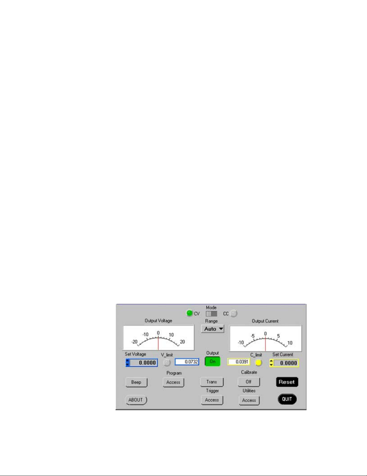
If the CAL:DPOT command was used to adjust the negative output, after adjusting the negative supply output, send CAL:LCURR MAX to the unit and repeat step 26 before proceeding
to step 29.
29.Set the BOP to current limit by sending CAL:CPR MAX. Continue to measure the output of
the BOP.
30.Send the command CAL:DATA -10 to decrease the voltage across the sense resistor until
the output voltage measured is within, or close to, the tolerance specified in Table 3-2 for
CURRENT LIMIT ADJUST. Send the command CAL:DATA 1 to increase the voltage or
CAL:DATA -1 to decrease the voltage as necessary until the measured value is within the
tolerance specified in Table 3-1 for CURRENT LIMIT ADJUST.
31.Save the calibration levels by sending CAL:SAVE 2/21/2004. The 9 characters at the end
are optional and are the calibration date of the power supply. The date entered in this manner is reported in the *idn? query. This can be prove useful for checking calibration dates
when periodic calibration is imposed by system or quality requirements.
3.3.2 CALIBRATION OF BIT 4886 INTERFACE CARD USING THE VISA DRIVER SOFT PANEL
Calibration of the BIT 4886 card installed in the BOP is performed using SCPI commands implemented through the Instrument driver. The driver provides a graphical interface with informational displays and prompts which lead you through the calibration of the BIT 4886 card. This
VISA compliant driver works with many GPIB cards from suppliers like National Instruments and
Hewlett-Packard.
NOTE: PC-12 connector (See Figure 2-2) must be installed for BOP to function.
The following calibration procedure uses the “soft” front panel which is part of the CVI driver for
the BIT 4886 which can be downloaded from the Kepco website at:
www.kepcopower.com/drivers.htm
Unzip the files and doubleclick on setup.exe to install the driver. The bit_mdac folder will be
added to the Start - Programs folder. Doubleclick bit_mdac.exe to run the program, and refer to
the visamdac.pdf in the bit_mdac folder for details about using the soft front panel.
FIGURE 3-3. MAIN PANEL
BIT 4886 120413 3-9
Page 32

3.3.2.1 CALIBRATION BASICS
CAUTION: Before performing calibration, set BOP OUTPUT to OFF and connect short
across BOP output, then set OUTPUT to ON and Voltage to 10V. It is necessary
to wait 10 minutes before calibrating the unit to allow for thermal stabilization. After 10 minutes, set OUTPUT to OFF and remove short from BOP output,
then proceed with calibration.
All adjustments are done using the six arrow buttons of the Calibration Panel (see Figure 3-4
and Table 3-4). The double arrow buttons
output five steps at a time; the " and # buttons either increase (#) or decrease (") the output one step at a time. The triple arrow buttons <<<— and —>>> either increase (—>>>) or
decrease (<<<—) the output 80 steps at a time The
the 80-step window established by <<<— and —>>>.
! and " either increase (") or decrease (!) the
!, ", ", and # buttons only work within
For MAX and MIN Calibrations fine adjustment is done using the
the value can not be set within the specified tolerance using the fine adjustment, use the coarse
adjustment to increase (—>>>) or decrease (<<<—) the output as needed, then use the fine
adjust buttons to set the value within tolerance. Where large adjustment is necessary, <<<—
and —>>> can be used first to bring the output close before using the
tons.
FIGURE 3-4. CALIBRATION PANEL
TABLE 3-4. CALIBRATION PANEL FUNCTIONS
!, ", ", and # buttons. If
!, ", ", and # but-
BUTTON OR WINDOW Function
START button Initiates calibration.
Text box (Adjacent to START button) Used to enter unit password.
VOLT button Initiates Voltage calibration.
CURR button Initiates Current calibration.
Message box (below VOLT buttons) Provides instructions about the calibration process.
White text window (above OK button) Displays the parameter currently being calibrated.
" button Fine Adjustment - Decreases the output value by one LSB.
# button Fine Adjustment - Increases the output value by one LSB.
! button Adjustment - Decreases the output value by five LSBs.
" button Adjustment - Increases the output value by five LSBs.
<<<— button Coarse Adjustment - Decreases the output value by 80 LSBs.
—>>> button Coarse Adjustment - Increases the output value by 80 LSBs.
OK button Enters the value displayed in the white text window.
3-10 BIT 4886 120413
Page 33

3.3.2.2 CALIBRATION PROCEDURE
1. Click on the Calibration Off button on the main panel (see Figure 3-4).This will open a cali-
bration panel (see Figure 3-4 and Table 3-4) that allows calibration in either voltage or current mode.
2. The password (DEFAULT) has been set at the factory. If it has not been changed, it will be
displayed in the box adjacent to the Start button on the right side of the panel. If the password has been changed from DEFAULT, substitute the proper password in the box adjacent
to the Start button and click the Start button. If the password has been forgotten, consult
factory. If the password is correct, the Volt and Curr buttons will become active. Otherwise
the message ERROR! - Wrong Password is displayed and you must enter the correct
password and click Start again.
3. For Voltage Calibration, click Volt button. The text window reads Volt ZERO and the mes-
sage Adjust for ZERO R81 (Eo Zero) on BOP A1 card. is displayed.
4. Connect a DVM to the output of the unit and adjust the R81 Potentiometer on A1 board of
BOP until the DVM reads the voltage specified in Table 3-1 for Low Range Zero, then click
OK button.
NOTE: Use external DVM for all measurements.
5. The text window reads Volt ZERO and the message Measure and Adjust. is displayed.
Using the " and # and
DVM reads the voltage specified in Table 3-1 for VOLT ZERO, then click OK button.
! and " buttons (see PAR. 3.3.2.1), adjust the output until the
6. The text window reads Volt MAX and the message Measure and Adjust. is displayed.
Using the " and # and
as specified in Table 3-1 for High Range Accuracy. Click OK when done.
7. The text window reads Volt MIN and the message Measure and Adjust. is displayed.
Using the " and # and
as specified in Table 3-1 for High Range Accuracy, then click OK button. NOTE: If the <<<—
or —>>> button is depressed, return to step 6 after clicking OK.
8. The text window reads LVolt MAX and the message Measure and Adjust. is displayed.
Using the " and # and
reads voltage specified in Table 3-1 for Low Range Accuracy, then click OK button.
9. The text window reads LVolt MIN and the message Measure and Adjust. is displayed.
Using the " and # and
age specified in Table 3-1 for Low Range Accuracy, then click OK button. NOTE: If the <<<—
or —>>> button is depressed, return to step 8 after clicking OK.
10.The text window reads Volt PROTECT and the message Measure and Adjust. is dis-
played. Using the " and # and
reading is as specified in Table 3-1. Click OK when done.
11. Voltage calibration is complete. If desired, the voltage calibration can be repeated by clicking
Volt at the calibration panel (Figure 3-4). If current calibration is not necessary, proceed to
step 23.
! and " buttons (see PAR. 3.3.2.1), adjust until DVM reading is
! and " buttons (see PAR. 3.3.2.1), adjust until DVM reading is
! and " buttons (see PAR. 3.3.2.1), adjust output until DVM
! and " buttons (see PAR. 3.3.2.1), adjust until DVM reads volt-
! and " buttons (see PAR. 3.3.2.1), adjust until DVM
BIT 4886 120413 3-11
Page 34

12.At the calibration panel (Figure 3-4) click CURR to begin current calibration of the unit. Con-
nect CALIBRATION RESISTOR! window opens.
13.Connect load (see Table 3-3) across the output of the unit and connect DVM across the load
as shown in Figure 3-2. Voltage measurements must be converted to Amperes using Ohm’s
law, E = IR. Click OK button to close Connect CALIBRATION RESISTOR window.
14.The test window reads LCurr ZERO and the message Adjust for ZERO R83 (Io Zero) on
BOP A1 card. will be displayed.
15.Adjust the R83 Potentiometer on A1 board of BOP, until the external DVM reads voltage
specified in Table 3-2, then click OK button.
16.The text window reads LCurr MAX and the message Measure and Adjust. is displayed.
Using the " and # and
reads voltage specified in Table 3-2 for Low Current Accuracy, then click OK button.
17.The text window reads LCurr MIN and the message Measure and Adjust. is displayed.
Using the " and # and
age specified in Table 3-2 for Low Current Accuracy, then click OK button. NOTE: If the
<<<— or —>>> button is depressed, return to step 16 after clicking OK.
18.The text window reads Curr ZERO and the message Measure and Adjust. is displayed.
Using the " and # and
DVM reads the voltage specified in Table 3-2 for Main Current Zero, then click OK button.
! and " buttons (see PAR. 3.3.2.1), adjust output until DVM
! and " buttons (see PAR. 3.3.2.1), adjust until DVM reads volt-
! and " buttons (see PAR. 3.3.2.1), adjust the output until the
19.The text window reads Curr MAX and the message Measure and Adjust. is displayed.
Using the " and # and
reads the voltage specified in Table 3-2 for High Current Accuracy, then click OK button.
20.The text window reads Curr MIN and the message Measure and Adjust. is displayed.
Using the " and # and
as specified in Table 3-2 for High Current Accuracy. NOTE: If the <<<— or —>>> button is
depressed, return to step 19 after clicking OK.
21.The text window reads Curr PROTECT and the message Measure and Adjust. is displayed. Using the " and # and
reading is as specified in Table 3-2. Click OK when done.
22.Current calibration is complete. If desired, the current calibration can be repeated by clicking
Curr at the calibration panel (Figure 3-4).
23.To exit Calibration, click on the Calibration On button on the main panel (Figure 3-3). This
will open a panel that allows the calibration to be saved. Click SAVE to save the calibration
constants (both voltage and current), or CANCEL to return to the old calibration.
! and " buttons (see PAR. 3.3.2.1), adjust output until DVM
! and " buttons (see PAR. 3.3.2.1), adjust until DVM reading is
! and " buttons (see PAR. 3.3.2.1), adjust until DVM
3-12 BIT 4886 120413
Page 35

SECTION 4 - OPERATION
4.1 GENERAL
The Kepco BOP Power Supply, with an installed BIT 4886 Interface Card, may be programmed
over the IEEE 488 standard communication bus (General Purpose Interface Bus, GPIB) using
SCPI (Standard Commands for Programmable Instruments). SCPI provides a common language used in an automatic test system. (Refer to Table 2-3 for input/output signal allocations.)
CAUTION: DO NOT repeatedly toggle the circuit breaker/switch as this may cause unit to fault.
Set Power ON/OFF circuit breaker/switch on front panel to ON. If actuator does not
lock when released, wait a few seconds before trying again. The circuit breaker is
“trip-free” design; if overload exists, contacts cannot be held closed by actuator.
NOTE: Upon power up, the BOP output is set to off, VOLTage and CURRent are set to 0.
VOLTage and CURRent commands will not change the BOP output until the command
OUTPut ON is sent to the BIT 4886.
4.1.1 PROGRAMMING TECHNIQUES TO OPTIMIZE POWER SUPPLY PERFORMANCE
Proper programming techniques can offer significant response time improvement and reduce
undesirable transients at the power supply output. The key to performance optimization is to
minimize mode changes (voltage mode/current limit to current mode/voltage limit or vice versa).
Mode changes should be limited to changes in load conditions (to which the power supply will
respond automatically), or by programming the limit parameter when required by the user application.
The proper way to program the power supply is to initially program the operating parameter to
zero and the complementary limit parameter to the desired maximum value. Subsequent commands should change only the operating parameter. (The operating parameter is the parameter
that controls the output, e.g., voltage controls the output in voltage mode, current in current
mode.) The complementary limit parameter should be programmed only when there is a need to
change it.
4.1.1.1 SETTING BOP VOLTAGE AND CURRENT LIMITS
There are no voltage or current protection settings that can be accessed through the GPIB interface. The limit controls on the BOP front panel (with the screw driver adjustment) can be used to
limit output voltage or current. The limit control settings from the BOP front panel are fixed and
are not computer-controllable. A common use of these controls is to set -V limit to 0 to prevent
the BOP from supplying a negative output voltage.
The BIT 4886 controls the BOP via two channels: the main channel, which is defined by the
operating mode, and the limit channel. In voltage mode, the main channel handles output voltage and the limit channel handles current limit. In current mode the main channel handles output current and the limit channel handles voltage limit.
• If the BOP is operating in voltage mode, sending VOLT sxxxx controls the main channel,
and thus the output voltage (where s = sign, + or – and xxxx = the absolute value of output voltage). Sending CURR sxxxx controls current limit (where s = sign, + or – and xxxx
= the absolute value of current limit.
• If the BOP is operating in current mode, sending CURR sxxxx controls the main channel,
BIT 4886 120413 4-1
Page 36

and thus the output current (where s = sign, + or – and xxxx = the absolute value of output current). Sending VOLT sxxxx controls voltage limit (where s = sign, + or – and xxxx
= the absolute value of voltage limit.
4.1.1.2 AUTOMATIC RANGE OPERATION.
The BIT 4886 has low and high ranges which are changed automatically when the main channel
set point is changed from a value less than the 1/4 of the units operating capability to a value
that is higher than 1/4 of the operating capability. The automatic gain change is enabled at
power up, or by either the *RST command or a mode change command (FUNC:MODE).
An automatic range change can result in undesirable transients when passing through the quarter scale point as result of BIT 4886 card gain change, depending upon the load at the output of
the BOP. For example, with a 50V BOP in voltage mode, the quarter scale gain change is at
12.5V. When the unit is programmed from 12.5V to 12.6V, the gain of the BOP changes and a
spike may be seen at the BOP output. A transient may also occur when changing from –5V
volts to +50V as –5 volts is in the region between –12.5V and +12.5V and +50V is beyond the
quarter scale region. When the unit is programmed to remain in full scale, the gain change
does not occur and this eliminates the transient.
4.1.1.3 USING THE BIT 4886 TO PRODUCE A SOFTWARE-TIMED RAMP AT THE BOP OUTPUT
If the power supply is intended to operate in a test application that requires a set of specific output voltages in a specific order and the number of points is more than the 1000 points available
in the BIT 4886 LIST command, a computer-controlled ramp can be used.
The recommended way to run a voltage ramp is to set the current limit to maximum plus at least
2% (or unit limit for max absolute value of the load). While in voltage mode, current limit is the
absolute value of the programmed current.
Before running the ramp it is recommended that the scale be set to full scale using
VOLT:RANG 1 to avoid any transients as explained in PAR. 4.1.1.2.
When installed, the Labview interactive example available on our web site creates a KpDCpwr
directory in Labview's user.lib. This sub-directory contains various programs such as KepcoDCPwr
Software Timed Ramp.vi. This vi is a software-timed linear ramp that is an example of using both
the range command and the limits in generating a ramp. There is also a KepcoDCPwr Software
Timed Current Ramp.vi for the same functionality in current mode.
4.1.2 MAKING SURE THE PREVIOUS COMMAND IS COMPLETE
Some SCPI commands require a flash memory update and can take an indeterminate amount
on time to complete. These commands are:
•*SAV
• MEM:PACK
• MEM:UPD
•CAL:COPY
•CAL:SAVE
• SYST:PASS:NEW
• SYST:SEC:IMM
When sending these commands via the GPIB, these commands require a query to be added to
the command string to verify the previous command is complete. When the command is complete, the unit updates the status byte and indicates MAV (Message Available, bit 4 - see Table
A-3) is true. MAV indicates that there is a response to be received by the computer, so when it
4-2 BIT 4886 120413
Page 37

becomes set, the unit is ready for its next command after reading back the data from the query
that was added to the command string.
When sending the above commands via the RS 232 bus, data flow control must be enabled
(XON) for the unit to properly update flash memory.
The *ESR? query is ideal to check if the previous command is complete since it returns either a
1 or 0. It is important that it be sent as a part of the same string as the command that causes a
flash update. As an example, sending CAL:SAVE 12/31/2005;:*esr? or *esr?;:CAL:SAVE 12/31/
2005 are valid command strings. Sending the commands separately will not verify that the previous command is complete. Figure 4-1 is a program written in C, incorporating these techniques.
Failure to provide an adequate delay can result in:
• Commands that are not processed,
• The following command may be received in error, causing an error in the transmission,
• Unit lock-up requiring power cycling of the unit. If working via the GPIB bus, sending
Interface Clear and Device Clear followed by *RST will unlock the unit.
BIT 4886 120413 4-3
Page 38

#include <formatio.h>
#include <utility.h>
#include <gpib.h>
#include <ansi_c.h>
/*Overhead for the use of a NATIONAL INSTRUMENTS gpib interface */
int unit_desc; // handle for the national instruments controller
int GPIbus=0; // GPIB card 0
int adr=6; // Power Supply address
char status_byte; // status byte from the power supply
#define MAV 0x10 /* bit 4 of the status byte is the Message AVailable bit by 488.2 specification */
/* Function Send_with_wait
INPUT: string to be sent to power supply
Description: adds the *ESR? query and performs serial polls to wait for the command to be completed.
*/
int Send_with_wait(char *command);
char snd[501]; // data to be sent to the power supply
char rcv [10]; // data from power supply
int j;
sprintf(snd,”%s;:*ESR?,command); // Add *ESR? to the command
Send(GPIbus, adr, snd, strlen(snd), 2); // Send the data to the power supply
for (j=0;j<500;j++)( // loop until ready (5 seconds max)
Delay(.05); // Wait for command to complete
ibrsp(unit_desc,&status_byte); // get status byte
if ((status_byte& 0x10) ==0x10) break;) // by looking for data in string
Receive (GPIbus, adr, rev, rev_buf_size,10); // so the error queue will not receive a 410 error
}
main( // test code to show operation of function.
unit_desc=ibdev(GPIbus,adr,adr/256,T100ms,1,0x40a);Delay(.005);
Send (GPIbus,adr,”VOLT 10;curr .01”,sizeof(“VOLT 10;curr .01”),NLEND;
Send_with_wait(“*SAV 10”);
}
// so there is a response from the
// power supply
FIGURE 4-1. PROGRAMMING EXAMPLE TO VERIFY PREVIOUS COMMAND HAS COMPLETED
4.2 INITIALIZATION OF THE BIT 4886 CARD
When a BIT 4886 Card is installed in a BOP it must be initialized prior to use. The initialization of
the BOP BIT card can be performed via either GPIB or RS 232 ports. The process can be
accomplished using the supplied computer program via the GPIB (see PAR. 4.2.1) or by sending SCPI commands using either the RS 232 or GPIB protocol (see PAR. 4.2.2).
4.2.1 INITIALIZATION USING CVI DRIVER - GPIB PORT ONLY
The initialization procedure uses the “soft” front panel which is part of the CVI driver for the BIT
4886. The CVI Driver can be downloaded from the Kepco website at: www.kepcopower.com/
4-4 BIT 4886 120413
Page 39

drivers.htm by choosing the appropriate model and CVI configuration. The CVI Driver can not
be used via the RS 232 Port.
1. Unzip the files and doubleclick on setup.exe to install the driver. The bit_mdac folder will be
added to the Start - Programs folder. Doubleclick bit_mdac.exe to run the program, and refer
to the visamdac.pdf in the bit_mdac folder for details about using the soft front panel.
2. Connect GPIB cable from the rear of the BOP with BIT 4886 Card installed to a Microsoft
Windows-based computer with National Instruments VISA software installed and verify that
BOP has standard PC-12 connector installed (Figure 2-2).
3. Install the VISA driver per the text file included with the driver. At the Start-up screen (Figure
4-2) set the correct GPIB Address and click CONNECT. Upon successful initialization the initialization window closes and the Power Supply Type field of the Start-up window (Figure 4-
2) shows BIT 4886. Click Continue.
FIGURE 4-2. VISA DRIVER START-UP
4. Refer to Figure 4-3 and enter the following information:
• Select Model: e.g., BOP 100-2.
• Serial Number: Enter serial number found on the rear nameplate of BOP power supply.
• Option Number: If unit is a special (modified) unit, enter 5-digit suffix found in the Manual Addendum
• Press the Initialize Card button
NOTE: If initialization fails and an error message is displayed, repeat step 3, making
sure that the proper information is entered
5. After initialization, proceed to PAR. 3.3.2 to calibrate the upgraded unit.
BIT 4886 120413 4-5
Page 40

FIGURE 4-3. BIT 4886 CARD INITIALIZATION USING VISA DRIVER
4.2.2 INITIALIZATION USING SCPI COMMANDS AND GPIB PORT
1. With the BOP power off, place the five address switches to the on position (see Figure 2-1
for switch location).
2. Insure a GPIB controller is connected to the BOP via the GPIB cable. Set BOP power to OFF
and set the address switches to the proper GPIB address to be used (refer to PAR 2.2.1, Figure 2-1, and Table 2-2 for addresses). Set BOP Power on; it may beep three times indicating
it is ready for initialization.
3. Using the GPIB interactive mode, set up the GPIB interface. For a National Instruments card,
it is done by the following steps.
A. Start the interactive GPIB program.
B. Type ibfind DEVx where x is the hex address of the BOP.
C. Type ibwrt "*idn?"
D. Type IBREAD 100. The GPIB will show the identifier string of the BOP as: KEPCO,
BOP 200-20, with additional characters indicating the revision level of the firmware.
4. Send the password initialization string of: SYST:PASS:CEN DEFAULT.
5. Send the BOP configuration code. The configuration code format is VOLTAGE,CURRENT;
for example the 100 Volt, 1 Amp BOP 100-1M is identified as 100,1. The sequence to be
sent is: DIAG:PST 100,1.
6. Calibrate the unit per PAR. 3.3. Failure to calibrate the unit will result in the *TST? query
reporting a FLASH memory error.
4-6 BIT 4886 120413
Page 41

7. After the calibration has been completed, the master calibration levels can be established
using the following command: CAL:COPY WORK FACT.
4.2.3 INITIALIZATION USING SCPI COMMANDS AND RS 232 PORT
1. With the BOP power off, place the five address switches to the on position (see Figure 2-1
for switch location).
2. Set BOP power to OFF and set the address switches to the proper GPIB address to be used
(refer to PAR 2.2.1, Figure 2-1, and Table 2-2 for addresses). Set BOP Power on; it may
beep three times indicating it is ready for initialization.
3. Set up the RS 232 interface as indicated by the following steps.
A. Start the Hyperterminal
B. Set Hyperterminal to direct connect at 9600 baud.
C. Type *idn?
D. Unit responds with the identifier string of the BOP, e.g.,: KEPCO, BOP 200-20, with
additional characters indicating the revision level of the firmware.
4. Send the password initialization string of: SYST:PASS:CEN DEFAULT.
5. Send the BOP configuration code. The configuration code format is VOLTAGE,CURRENT;
for example the 100 Volt, 1 Amp BOP 100-1M is identified as 100,1. The sequence to be
sent is: DIAG:PST 100,1.
6. Calibrate the unit per PAR. 3.3. Failure to calibrate the unit will result in the *TST? query
reporting a FLASH memory error.
7. After the calibration has been completed, the master calibration levels can be established
using the following command: CAL:COPY WORK FACT.
4.2.4 PASSWORD SETUP.
To change a password send:
SYST:PASS:CEN DEFAULT
SYST:PASS:NEW DEFAULT new_password
4.2.4.1 FORGOTTEN PASSWORDS
If the password is lost, it is possible to enable the password interface by sending
SYST:PASS:CEN POWERSUPPLIER
Once enabled, the password can be set to DEFAULT by sending
BIT 4886 120413 4-7
Page 42

SYST:SEC:OVERRIDE
4.3 BUILT IN TEST
The BIT 4886 card is designed to perform periodic testing of itself, power up testing and commanded testing. The testing is reported to the operator both by errors placed in the SCPI error
queue and by issuing audible beeps.
The driver and demonstration soft panel which can be downloaded from the Kepco website at:
www.kepcopower.com/drivers.htm provide an easy way to verify BIT 4886 performance. A
description of the driver is included as an Adobe Acrobat ™ PDF file.
4.3.1 POWER-UP TEST
The power up testing of the BIT 4886 is similar to the *TST command (PAR. A.16). Portions of
the card are verified on power-up and errors are indicated by the beep codes listed in Table 4-1.
The failed test is repeated indefinitely. The power-up test can be bypassed by placing all DIP
switch positions of address switch S1 to up (ON, 1). Once bypassed, the unit beeps on and off
at equal intervals to indicate the address switches are set to 1 and the unit is waiting for the
address switches to be set to a valid GPIB address.
4.3.2 CONFIDENCE TEST
The SCPI command *TST? Is used to perform a confidence test of the interface. It verifies the
microprocessor memory, the timer, optical buffer and reference of the BIT 4886 card. It does not
affect the output of the BOP. This command returns a 0 for pass and number from 1 through
1023 to indicate the cause of the error. The test executes each of the subtests even when any
one fails. If any test fails a bit is set in the error code which is returned to the user. The error
codes returned are listed in Table 4-1
TABLE 4-1. BUILT-IN TEST ERROR CODES
TEST ACTIVE ERROR CODES
*tst? DIAG:TST? BIT VALUE BEEPS
Yes Yes 0 Pass (No error)
Yes Yes 0 1 1 ROM error
Yes Yes 1 2 1 RAM error
Yes Yes 2 4 2 FLASH error -- Perform calibration to correct
Yes Yes 3 8 3 Optical Buffer Error‘
Yes Yes 4 16 6 Digital Pot error
No Yes 5 32 5 Loop Back Test error
No Yes 6 64 Max Voltage Output error
No Yes 7 128 Min Voltage Output error
No Yes 8 256 1/4 Scale Voltage error
No Yes 9 512 1/4 Scale Voltage Readback error
MEANING
4-8 BIT 4886 120413
Page 43

4.3.3 BOP TEST
The DIAG:TST? Command performs a test of the BOP instrument. The test includes the BIT
4886 internal tests of the DAC (Digital to Analog Converter), Limit and Op Amp circuits. If successful it programs the BOP in voltage mode to the positive and negative limits of the device. It
also verifies the Limit operation of the unit in current mode by setting the unit for the rated maximum current delivery and verifies that the voltage limit set at one volt operates correctly. It also
tests the readback voltages in both high and low scales.
CAUTION: TO AVOID DAMAGE TO THE LOAD, DISCONNECT THE LOAD BEFORE ISSU-
ING THIS COMMAND. (DURING THE SELF-TEST, THE BOP IS PROGRAMMED TO FULL SCALE POSITIVE AND FULL SCALE NEGATIVE
OUTPUT.)
This command returns a 0 for pass, or a number from 1 through 1023 to indicate the cause of
the error. The test executes each of the subtests even when any one fails. If any test fails, a bit
is set in the error code which is returned to the user. The error codes returned are listed in Table
4-1.
4.4 IEEE 488 (GPIB) BUS PROTOCOL
Table 4-2 defines the interface capabilities of the Interface Card (Talker/Listener) relative to the
IEEE 488 (GPIB) bus (reference document ANSI/IEEE Std 488: IEEE Standard Digital Interface for
Programmable Instrumentation) communicating with a Host Computer–Controller (Talker/Listener).
TABLE 4-2. IEEE 488 (GPIB) BUS INTERFACE FUNCTIONS
FUNCTION
Source Handshake SH1 Complete Capability (Interface can receive multiline messages).
Acceptor Handshake AH1 Complete Capability (Interface can receive multiline messages).
Ta lk er T 6
Listener L4 Basic listener, unaddress if MTA (My Talk Address) (one-byte address).
Service Request SR1
Remote/Local RL2 No Local lock-out.
Parallel Poll PP0 No Capability.
Device Clear DC1
Device Trigger DT1 Complete Capability.
Controller C0 No Capability.
SUBSET
SYMBOL
Basic talker, serial poll, unaddress if MLA (My Listen Address) (one-byte
address).
Complete Capability. The interface sets the SRQ line true if there is an
enabled service request condition.
Complete Capability. Controller sends DCL (Device Clear) and SDC
(Selected Device Clear) to selected power supply.
COMMENTS
Tables 4-3 and 4-4 define the messages sent to the Interface Card, or received by the Interface
Card, via the IEEE 488 bus in IEEE 488 command mode and IEEE 488 data mode, respectively.
BIT 4886 120413 4-9
Page 44

These messages are enabled during the “handshake” cycle, with the Interface Card operating
as either a Talker or a Listener.
4.5 RS232-C OPERATION
The BIT 4886 card allows the BOP to be operated via an RS232-C terminal, or from a PC using
a terminal emulation program. The default settings are as follows:
• Baud rate: 9600
• Parity: None
•Data Bits8
• Stop Bits 1
• Echo ON
•XON OFF
To change echo or XON/XOFF, refer to PAR. 4.5.2.
TABLE 4-3. IEEE 488 (GPIB) BUS COMMAND MODE MESSAGES
MNEMONIC MESSAGE DESCRIPTION COMMENTS
ATN Attention Received
DAC Data accepted Received or Sent
DAV Data Valid Received or Sent
DCL Device Clear Received
GET Group Executive Trigger Received
IFC Interface Clear Received
MLA My Listen Address Received
MTA My Talk Address Received
OTA Other Talk Address Received
RFD Ready for Data Received or Sent
SDC Selected Device Clear Received
SPD Serial Poll Disable Received
SPE Serial Poll Enable Received
SRQ Service Request Sent
UNL Unlisten Received
UNT Untalk Received
4-10 BIT 4886 120413
Page 45

TABLE 4-4. IEEE 488 (GPIB) BUS DATA MODE MESSAGES
MNEMONIC MESSAGE DESCRIPTION COMMENTS
DAB
END
EOS
RQS
STB
4.5.1 SERIAL INTERFACE
The serial interface behaves like the GPIB interface in that the command is parsed after receiving a control character of either a Line Feed or Carriage Return. The serial interface supports six
special control characters. The six special control characters are:
Escape (1B
Backspace (08
) Causes the input buffer to be cleared. This character is used to ensure
H
) Causes the last character in the input buffer to be removed from the
H
Carriage Return (0D
Data Byte Received or Sent
End Received or Sent
End of String Received or Sent
Request Service Sent
Status Byte Sent
that the buffer is empty when the host powers on since it is possible
that the Interface Card was previously powered on and received some
characters prior to the initialization of the host computer.
input buffer queue.
) Causes the input buffer to be parsed by the BOP.
H
Line Feed (0A
) Causes the input buffer to be parsed by the BOP.
H
4.5.2 RS 232 IMPLEMENTATION
The following paragraphs are provided to help the user understand how the RS 232 serial interface is implemented in the BIT 4886. Since the RS 232 protocol does not use a parity bit, the
echo mode is the default method used to ensure reliable communication between the command
originator (computer) and the BIT 4886, thus avoiding a more complex “handshake” protocol.
When the BIT 4886 is in the RS 232 echo mode it returns all data sent to the host controller. The
BIT 4886 provides one additional option that allows handshake communication: the XON XOFF
method. In standard echo mode the controller must verify that each character is echoed back by
the BIT 4886. As shown in Figure 4-4, there are times when the BIT 4886 does not echo back
the character from the controller, requiring that the controller resend the character. By using the
handshake option (XON XOFF) the host controller can ensure that serial data interrupts occurring after parsing of the incoming message do not result in lost data.
Figure 4-4 illustrates the default echo mode and the XON XOFF method described in the following paragraphs.
BIT 4886 120413 4-11
Page 46

FIGURE 4-4. RS 232 IMPLEMENTATION
Only seven control characters (characters between 00H and 1FH) are acknowledged by the BIT
4886:
• Carriage Return (CR, 0D
• Line Feed (LF, 0A
)
H
• Back Space (BS, 08
• Escape (ESC, 01B
•XON (011
•XOFF (013
• CAN (018
)
H
H
)
H
H
)
)
H
)
H
)
BS deletes the last character entered, with the exception of CR or LF characters. Either the CR
or LF character acts as the line terminator, initiating parsing of the ASCII data sent to the BIT
4886 by the command originator. When the line is parsed and the commands are sent to the
analog processor, the BIT 4886 sends the line terminator sequence CR LF to the command
originator.
The ESC character is used for synchronization, causing the BIT 4886 to reset its input buffer
and return a CR LF sequence.
The XON character enables the transmitter if XON/XOFF flow control is enabled (see PAR.
4.5.2.2).
The XOFF character stops data transmission if XON/XOFF flow control is enabled (see PAR.
4.5.2.2).
The CAN character resets the receive and transmit pointers and queues.
CAUTION: When the serial port has received an XOFF, the error message -400, QUE
error will be placed in the queue to indicate the loss of transmitted informa-
tion due to a received XOFF character. When XON is received, the unit will
transmit all data in it's buffer followed by the exclamation character (!). This
(!) character is not part of any message from the BIT 4886 and indicates the
transmission buffer has been cleared and the BIT 4886 is idle.
4-12 BIT 4886 120413
Page 47

All non-control characters are sent via the serial port of the command originator. The control
character BS is echoed as BS Space BS. Only the first control character is returned in response
to either a CR LF or LF CR character sequence (see Figure 4-4).
4.5.2.1 ECHO MODE
Echo mode is one method of ensuring data is transferred without errors. This mode should only
be enabled when errors in operation are detected. Refer to PAR. B.76 to change the setting.
Each byte (character) is echoed back to the sender where it is verified as the same character
that was just sent. If the wrong character is echoed back, sending the ESC character clears the
line to allow retransmission of the character. It is important that CR and LF characters are NOT
sent until the verification process is complete.
When working in echo mode, it is possible to receive the NAK (15 hex) from the BIT 4886. This
indicates an unknown quantity of echoed characters have been lost due to a queue overflow
problem. The error queue will also contain the -400, QUE error message, To prevent this,
please insure the received data string does not exceed 127 characters between line terminators
and no more than four queries are sent between line terminators in SCPI mode of operation
All non-control characters are sent via the serial port of the command originator.
4.5.2.2 XON XOFF METHOD
The XON XOFF method allows the BIT 4886 to control when the command originator is allowed
to send data. The command originator can only send data after the XON (transmission on) character (011
) has been received; the command originator stops sending data after receiving the
H
XOFF (transmission off) character (013
sending additional data. Refer to PAR. B.78 to change the setting.
), and waits until the XON character is received before
H
Control characters, either CR or LF, are returned as XOFF CR if echo mode is on, and as XOFF
if echo mode is off. XOFF stops data from the command originator and the BIT 4886 returns the
normal sequence of CR LF (if echo mode is enabled).
4.5.2.3 ISOLATING RS 232 COMMUNICATION PROBLEMS
A Loop Back test can be executed to aid in isolating RS 232 communication problems. The test
is executed via a SCPI command sent over the GPIB interface.
1. Send the command DIAG:LBT? to the unit via the GPIB interface with the Loop Back Test
connector (Kepco P/N 195-0111) NOT installed. The response sent over the GPIB will be
FAI LED.
2. Install the Loop Back Test connector (Kepco P/N 195-0111) into the RS 232 port; if this connector is not available, skip this step and proceed to step 3. Send DIAG:LBT? again and
read back the answer. if the response is PASSED, the power supply is operating properly. If
the response is FAILED, the unit requires repair.
3. To test the integrity of the cable assembly connecting the BIT 4886 RS 232 port to the computer, remove the Loop Back test connector from the BIT 4886 RS 232 port and connect the
cable in its place. With the DB9 adapter installed on the opposite end of the cable, connect a
short jumper wire between pins 2 and 3 of the adapter connector and repeat the test of step
2 above. If the response is FAILED, the cord is either an improper type (not null modem) or
BIT 4886 120413 4-13
Page 48

defective. If the response is PASSED, the cable is correct; remove the jumper and reconnect
the cable to the computer.
4. If the loop back connector was not available and steps 1 And 3 were completed successfully,
contact Kepco to obtain loop back connector P/N 195-0111 and rerun the test. If each of the
above steps is completed successfully, the problem lies in the computer hardware and/or
software. If the serial communication is monitored at the computer end, every DIAG:LBT?
command will cause the IDN response to be sent to the computer.
4.5.3 USING SCPI COMMANDS FOR RS 232 COMMUNICATION.
The unit must be in remote mode before RS 232 commands affecting the output can be executed (e.g., VOLT 10;OUTP ON). This can be accomplished by sending SYST:REM ON prior to
sending any commands that affect the power supply output. (See PAR. B.87 and Figure B-7)
4.6 SCPI PROGRAMMING
SCPI (Standard Commands for Programmable Instruments) is a programming language conforming to the protocols and standards established by IEEE 488.2 (reference document ANSI/
IEEE Std 488.2, IEEE Standard Codes, Formats, Protocols, and Common Commands). SCPI commands are sent to the Interface Card as output strings within the selected programming language (PASCAL, BASIC, etc.) in accordance with the manufacturer’s requirements for the
particular GPIB interface card used.
Different programming languages (e.g., BASIC, C, PASCAL, etc.) have different ways of representing data that is to be put on the IEEE 488 bus. It is up to the programmer to determine how
to output the character sequence required for the programming language used. Address information (GPIB address) must be included before the command sequence. (See PAR. 2.2.1 to
establish the Interface Card GPIB address.)
4.6.1 SCPI MESSAGES
There are two kinds of SCPI messages: program messages from controller to power supply,
and response messages from the power supply to the controller. Program messages consist of
one or more properly formatted commands/queries and instruct the power supply to perform an
action; the controller may send a program message at any time. Response messages consist of
formatted data; the data can contain information regarding operating parameters, power supply
state, status, or error conditions.
4.6.2 COMMON COMMANDS/QUERIES
Common commands and queries are defined by the IEEE 488.2 standard to perform overall
power supply functions (such as identification, status, or synchronization) unrelated to specific
power supply operation (such as setting voltage/current). Common commands and queries are
preceded by an asterisk (*) and are defined and explained in Appendix A. Refer also to syntax
considerations (PARs. 4.6.2 through 4.6.5).
4.6.3 SCPI SUBSYSTEM COMMAND/QUERY STRUCTURE
Subsystem commands/queries are related to specific power supply functions (such as setting
output voltage, current limit, etc.) Figure 4-5 is a tree diagram illustrating the structure of SCPI
subsystem commands used in the Interface Card with the “root” at the left side, and specific
commands forming the branches. The following paragraphs introduce the subsystems; subsystem commands that are defined and explained in Appendix B.
4-14 BIT 4886 120413
Page 49

ROOT : (colon)
INITiate subsystem
INITiate
[:IMMediate]
:CONTinuous
MEASure subsystem
MEASure
:CURRent?
:VOLTage?
[SOURce:] subsystem
[SOURce:]
VOLTage
[:LEVel]
[:IMMediate]
:TRIGgered
:MODE (LIST|FIX|TRANS val)
:RANGe
:RANGe:AUTO
CURRent
[:LEVel]
[:IMMediate]
:TRIGgered
:MODE (LIST|FIX|TRANS val)
:RANGe
:RANGe:AUTO
FUNCtion
:MODE (VOLT|CURR)
:TRIGgered
OUTPut subsystem
OUTPut
[:STATe] ON or OFF
CALibrate subsystem
CALibrate
:STATus <boolean>
:STATus?
:VOLT
:LEVel (MIN | MAX, ZERO)
[:DATA] val
GAIN (UP | DOWN)
:VPR (MIN | MAX)
:CPR (MIN | MAX)
:CURR
:LEVel (MIN | MAX, ZERO)
[:DATA] val
:GAIN (UP | DOWN)
:DPOT val
:LCURR (MIN | MAX, ZERO)
:LVOLT (MIN | MAX, ZERO)
:ZERO
:SAVE
LIST subsystem
LIST
:CLEar
:COUNt val
:COUNt:SKIP val
:CURRent val,val
:POINts?
:DIRection (UP|DOWN)
:DWELl val,val
:POINts?
:GENeration (SEQ|DSEQ)
:QUERy val
:VOLTage val,val
:POINts?
:SEQuence val,val
STATus subsystem
STATus
:OPERation
:CONDition?
:ENABle
[:EVENt]?
:PRESet
:QUEStionable
:CONDition?
:ENABle
[:EVENt]?
SYSTem subsystem
SYSTem
:BEEP
:COM
:SER
:ECHO, ?
:PACE, ?
:ERRor
[:NEXT]?
:CODE?
[:NEXT]?
:ALL?
:PASSword
[:CENAble] (code)
:STATe?
:CDISable (code)
:NEW (OLD | NEW)
:SECUrity
:IMMediate
:REM, ?
:SET
:VERSion?
FIGURE 4-5. TREE DIAGRAM OF SCPI COMMANDS USED WITH BIT 4886 INTERFACE CARD
4.6.3.1 INITIATE SUBSYSTEM
This subsystem enables the trigger system. When a trigger is enabled, the triggering action will
occur upon receipt of a GPIB <GET>, *TRG or TRIGger command. If a trigger circuit is not
enabled, all trigger commands are ignored.
4.6.3.2 MEASURE SUBSYSTEM
This query subsystem returns the voltage and current measured at the power supply's output
terminals.
BIT 4886 120413 4-15
Page 50

4.6.3.3 [SOURCE:]VOLTAGE AND [SOURCE:]CURRENT SUBSYSTEMS
These subsystems program the output voltage and current of the power supply.
4.6.3.4 OUTPUT SUBSYSTEM
This subsystem enables/disables the power supply output. Voltage and current are determined
by the combination of SOURCE subsystem VOLTage and CURRent commands and the load.
4.6.3.5 LIST SUBSYSTEM
The LIST subsystem is used to generate transients, waveforms and execute a series of steps
repeatedly. Up to 1002 power supply settings can be stored temporarily. Each setting consists of
either a voltage or current value (depending on whether the power supply has been set to Voltage or Current mode), and a corresponding dwell time (the duration those settings are in effect).
These settings may be executed in sequence as they are entered, or executed in a user-determined sequence that also allows individual settings to be repeated more than once. In addition,
the entire sequence may be repeated for a specific number of times, or run indefinitely until
commanded to stop. The sequence can also be run in reverse order to produce inverted waveforms. The following paragraphs provide guidance for using the list commands.
4.6.3.5.1 REQUIRED LIST COMMANDS
There are only five LIST commands, plus either the VOLT:MODE or CURR:MODE command,
that are needed to create and execute a list. Use of these required commands is illustrated in
Figure B-2 which shows the creation of sawtooth and triangular waveforms. LIST commands
are not accepted while a list is running. Send VOLT:MODE FIX (PAR. B.59) or CURR:MODE
FIX (PAR. B.50) to stop the list. A list remains in memory until the power is cycled or the
LIST:CLEAR command is processed. Therefore, if the original list is unchanged, additional commands can be added to the end of the list without resending all the commands. However, to
change parameters of one or more commands within the list, send LIST:CLEAR and then
resend the entire list including the changed parameters. To execute the list again, either
VOLT:MODE LIST or CURR:MODE LIST must be sent again.
LIST:VOLT (PAR. B.45) or LIST:CURR (PAR. B.31). These commands establish the points
(steps) of a list which program output voltage or current. A list can only be either a voltage list or
a current list, so the points in a list must be made with either LIST:VOLT XXXX or LIST:CURR
XXXX. Mixing of these commands within a list is not allowed.
LIST:CLEAR (PAR. B.26). Always precede a new list with this command. A list remains in memory until the power is cycled or the LIST:CLEAR command is processed.
LIST:DWELL (PAR. B.36). Defines the dwell time for each point in a list. In many instances it is
easier to use one dwell time and repeat a specific point multiple times to generate longer duration pulses. Remember, if more than one LIST:DWELL is sent, there must be a LIST:DWELL for
each voltage or current point in the list.
LIST:COUNT (PAR. B.27) Defines how many times a list is executed. 0 equals indefinite; when
a count of 0 is used, either *RST, VOLT:MODE FIX or CURR:MODE FIX must be used to stop
the list. *RST will cause the output to be set off and the unit is set to Voltage mode. VOLT:MODE
FIX or CURR:MODE FIX stops the list immediately; the point being executed when the list is
stopped will be present at the BOP output.
4-16 BIT 4886 120413
Page 51

4.6.3.5.2 OTHER REQUIRED COMMANDS
VOLT:MODE LIST (PAR. B.59) or CURR:MODE LIST (PAR. B.50). These commands start the
list and VOLT:MODE FIX (PAR. B.59) or CURR:MODE FIX (PAR. B.50) stop the list. LIST commands are not accepted while a list is running. If LIST:COUNT is between 1 and 255, when the
count decrements to 0, the list stops and the unit automatically moves to VOLT:MODE FIXED or
CURR:MODE FIXED state. To execute the list again, either VOLT:MODE LIST or CURR:MODE
LIST must be sent again.
4.6.3.5.3 OTHER USEFUL COMMANDS
LIST:COUNT:Skip (PAR. B.29). This command provides the ability to execute the initial points
only once whenever a list is run. It is used to set initial preconditions prior to running a repetitive
sequence.
LIST:DIR (PAR. B.34) This command changes the order of the list.
LIST:VOLT:POINTS? (PAR. B.47) or LIST:CURR:POINTS? (PAR. B.33) These queries return
the number of points in a list and provide a simple way to insure that all points entered were
properly processed and as intended.
4.6.3.5.4 OPTIONAL COMMANDS
Most commands have associated Queries (?) These are useful for troubleshooting/debugging
lists but are not needed in most cases.
The LIST:SEQ command is provided for backward compatibility. It is not recommended to be
used in any new designs as it may be eliminated at some point in the future.
4.6.3.6 STATUS SUBSYSTEM
This subsystem programs the power supply status register. The power supply has two groups of
status registers: Operation and Questionable. Each group consists of three registers: Condition,
Enable, and Event.
4.6.3.7 SYSTEM SUBSYSTEM
This subsystem is used to establish system settings Program Message Structure.
4.6.4 PROGRAM MESSAGE STRUCTURE
SCPI program messages (commands from controller to power supply) consist of one or more
message units ending in a message terminator (required by Kepco power modules). The message
terminator is not part of the syntax; it is defined by the way your programming language indicates the end of a line (such as a “newline” or “end-of-line” character). The message unit is a
keyword consisting of a single command or query word followed by a message terminator (e.g.,
CURR?<NL> or TRIG<end-of-line>). The message unit may include a data parameter after the
keyword separated by a space; the parameter is usually numeric (e.g., CURR 5<NL>), but may
also be a string (e.g., OUTP ON<NL>). Figure 4-6 illustrates the message structure, showing
how message units are combined. The following subparagraphs explain each component of the
message structure.
BIT 4886 120413 4-17
Page 52

NOTE: An alternative to using the message structure for multiple messages defined in the fol-
lowing paragraphs is to send each command as a separate line. In this case each command must use the full syntax shown in Appendix B.
KEYWORD
ROOT SPECIFIER
MESSAGE UNIT SEPARATOR
DATA
DATA SEPARATOR
KEYWORD
KEYWORD SEPARATOR
KEYWORD
INITIAL ROOT
SPECIFIER IS
:CURR:LEV 3.5;:OUTP ON;:CURR?<NL>
OPTIONAL
DATA SEPARATOR
DATA
MESSAGE UNIT SEPARATOR
ROOT SPECIFIER
KEYWORD
QUERY INDICATOR
MESSAGE TERMINATOR
MESSAGE UNIT
FIGURE 4-6. MESSAGE STRUCTURE
4.6.4.1 KEYWORD
Keywords are instructions recognized by a decoder within the Interface Card, referred to as a
“parser.” Each keyword describes a command function; all keywords used by the Interface Card
are listed in Figure 4-5.
Each keyword has a long form and a short form. For the long form the word is spelled out completely (e.g. STATUS, OUTPUT, VOLTAGE, and TRIGGER are long form keywords). For the
short form only the first three or four letters of the long form are used (e.g., STAT, VOLT, OUTP,
and TRIG).
To identify the short form and long form in this manual, keywords are written in upper case letters to represent the short form, followed by lower case letters indicating the long form (e.g.,
IMMediate, EVENt, and OUTPut). The parser, however, is not sensitive to case (e.g., outp,
OutP, OUTPUt, ouTPut, or OUTp are all valid).
You must use the rules above when using keywords. Using an arbitrary short form such as
ENABL for ENAB (ENABLE) or IMME for IMM (IMMEDIATE) will result in an error. Regardless
of which form chosen, you must include all the letters required by that form.
4-18 BIT 4886 120413
Page 53

4.6.4.2 KEYWORD SEPARATOR
If a command has two or more keywords, adjacent keywords must be separated by a colon (:)
which acts as the keyword separator (e.g., CURR:LEV:TRIG). The colon can also act as a root
specifier (paragraph 4.6.4.7).
4.6.4.3 QUERY INDICATOR
The question mark (?) following a keyword is a query indicator. This changes the command into
a query. If there is more than one keyword in the command, the query indicator follows the last
keyword. (e.g., VOLT? and MEAS:CURR?).
4.6.4.4 DATA
Some commands require data to accompany the keyword either in the form of a numeric value
or character string. Data always follows the last keyword of a command or query (e.g.,
VOLT:LEV:TRIG 14 or SOUR:VOLT? MAX.
4.6.4.5 DATA SEPARATOR
Data must be separated from the last keyword by a space (e.g., VOLT:LEV:TRIG 14 or
SOUR:VOLT? MAX.
4.6.4.6 MESSAGE UNIT SEPARATOR
When two or more message units are combined in a program message, they must be separated
by a semicolon (;) (e.g., VOLT 15;MEAS:VOLT? and CURR 12;CURR:TRIG 12.5).
4.6.4.7 ROOT SPECIFIER
The root specifier is a colon (:) that precedes the first keyword of a program message. This
places the parser at the root (top left, Figure 4-5) of the command tree. Note the difference
between using the colon as a keyword separator and a root specifier in the following examples:
VOLT:LEV:IMM 16 The root specifier is not necessary for the first keyword and has been
omitted. Both colons are keyword separators.
:CURR:LEV:IMM 4 Even though it is not required, it is still correct to include the root specifier
(first colon). The other two are keyword separators.
VOLT:LEV 6;:CURR:LEV 15 The root specifier for VOLT is not necessary because it is the
first keyword in the string and has not been included. The second colon is the root specifier for
CURR and is required; if it is missing an error will result. The first and third colons are keyword
separators.
:INIT ON;:TRIG;:MEAS:CURR?;VOLT? The first three colons are root specifiers. The
fourth colon is a keyword separator.
4.6.4.8 MESSAGE TERMINATOR
The message terminator defines the end of a message. Three message terminators are permitted:
• new line (<NL>), ASCII 10 (decimal) or 0A (hex)
BIT 4886 120413 4-19
Page 54

• carriage return (<CR>), ASCII 13 (decimal) or 0D (hex)
• both of the above (<CR> <NL>). If both are sent, the second is null and has no effect.
Your GPIB interface card software will automatically send a message terminator. For example,
the HP BASIC OUTPUT statement inserts <NL> after the last data byte. When binary data is
exchanged, <END> must be used. The combination <NL><END> terminator can be used for all
data except binary data.
NOTE: Kepco power modules require a message terminator at the end of each program mes-
sage. The examples shown in this manual assume a message terminator will be added
at the end of each message. Where a message terminator is shown it is represented
as <NL> regardless of the actual terminator character.
4.6.5 UNDERSTANDING THE COMMAND STRUCTURE
Understanding the command structure requires an understanding of the subsystem command
tree illustrated in Figure 4-5. The “root” is located at the top left corner of the diagram. The
parser goes to the root if:
• a message terminator is recognized by the parser
• a root specifier is recognized by the parser
Optional keywords are enclosed in brackets [ ] for identification; optional keywords can be
omitted and the power supply will respond as if they were included in the message. The root
level keyword [SOURce] is an optional keyword. Starting at the root, there are various
branches or paths corresponding to the subsystems. The root keywords for the Interface Card
are :INITiate, :MEASure, :OUTPut, [:SOURce], :STATus, and :SYSTem. Because the
[SOURce] keyword is optional, the parser moves the path to the next level, so that VOLTage,
CURRent, and FUNCtion commands are at the root level.
Each time the parser encounters a keyword separator, the parser moves to the next indented
level of the tree diagram. As an example, the STATus branch is a root level branch that has
three sub-branches: OPERation, PRESet, and QUEStionable. The following illustrates how
SCPI code is interpreted by the parser:
STAT:PRES<NL>
The parser returns to the root due to the message terminator.
STAT:OPER?;PRES<NL>
The parser moves one level in from STAT. The next command is expected at the level defined
by the colon in front of OPER?. Thus you can combine the following message units
STAT:OPER? and STAT:PRES;
STAT:OPER:COND?;ENAB 16<NL>
After the OPER:COND? message unit, the parser moves in one level from OPER, allowing the
abbreviated notation for STAT:OPER:ENAB.
4.6.6 PROGRAM MESSAGE SYNTAX SUMMARY
• Common commands begin with an asterisk (*).
• Queries end with a question mark (?).
• Program messages consist of a root keyword and, in some cases, one or more message
4-20 BIT 4886 120413
Page 55

units separated by a colon (:) followed by a message terminator. Several message units
of a program message may be separated by a semicolon (;) without repeating the root
keyword.
• If a program message has more than one message unit, then a colon (:) must precede
the next keyword in order to set the parser back to the root (otherwise the next keyword
will be taken as a subunit of the previous message unit).
e.g., the command meas:volt?;curr? will read output voltage and output current
since both volt? and curr? are interpreted as subunits of the meas command.
• Several commands may be sent as one message; a line feed terminates the message.
Commands sent together are separated by a semicolon (;). The first command in a message starts at the root, therefor a colon (:) at the beginning is not mandatory.
e.g., the command meas:volt?;curr? will read output voltage and output current,
however the command meas:volt?;:curr? will read actual output voltage and pro-
grammed current since the colon preceding curr? indicates that curr? is not part of the
meas command and starts at the root.
• UPPER case letters in mnemonics are mandatory (short form). Lower case letters may
either be omitted, or must be specified completely (long form)
e.g., INSTrument (long form) has the same effect as INST (short form).
• Commands/queries may be given in upper/lower case (long form)
e.g., SoUrCe is allowed.
• Text shown between brackets [] is optional.
e.g., [SOUR:]VOLT[:LEV]:TRIG has the same effect as VOLT:TRIG
4.6.7 SCPI PROGRAM EXAMPLE
Figure 4-7 is an example of a program written in C using SCPI commands to program a BOP
Power Supply. The program illustrated is for a configuration using a National Instruments GPIB
interface card. (It will be necessary to consult the manufacturer’s data to achieve comparable
functions with an interface card from a different manufacturer.) This program sets output voltage
(Voltage mode) or voltage limit (Current mode) to 5V, and current limit (Voltage mode) or output
current (Current mode) to 1A, then reads the measured (actual) voltage and current, then prints
the measurements.
4.7 ENHANCED OPERATION
The following paragraphs describe options that will permanently modify the behavior of the BIT
4886 and associated BOP power supply. Although these options use SCPI commands, they are
not intended to be used during normal programming of the BOP output.
The commands described in the following paragraphs affect only RAM variables. The power up
state of the variables is retrieved from the FLASH EEPROM. The command MEMORY:UPDATE
can be used to copy this RAM information to the FLASH EEPROM. The WINDOW variable is
stored using the command MEM:UPDATE SHUTDOWN and the other variables, including the
DIAG:SAV command, use the command MEMORY:UPDATE INTERFACE
BIT 4886 120413 4-21
Page 56

/**************************************************************************/
/* Sample Program (written in C) for KEPCO power supply using */
/* National Instruments GPIB interface card */
/**************************************************************************/
#include <stdio.h>
#include "decl.h"
char rd_str[80]; // Input buffer
char dat_str[80]; // Output buffer
int bd,adr;
main() {
adr = ibfind("DEV6"); // Open DEV6 (defined by IBCONF)
bd = ibfind ("GPIB0"); // Open GPIB card
ibsic (bd); // Send Interface Clear
strcpy(dat_str,"OUTPUT ON"); // SCPI default is Output off
ibwrt(adr,dat_str,strlen(dat_str)); // Power supply is
// in voltage mode
// outputing 0 volts
strcpy(dat_str,"VOLT 5;CURR 1"); // Define a set command
ibwrt(adr,dat_str,strlen(dat_str)); // Send string to power supply
strcpy(dat_str,"MEAS:VOLT?;CURR?"); // Define a measure command
ibwrt(adr,dat_str,strlen(dat_str)); // Send string to power supply
strset(rd_str,'\0'); // Clear input buffer
ibrd(adr,rd_str,64); // Read result of measure
printf("received : %s\n",rd_str); // Print voltage and current
}
/**************************************************************************/
FIGURE 4-7. TYPICAL EXAMPLE OF INTERFACE CARD PROGRAM USING SCPI COMMANDS
4.7.1 ERROR DETECTION
The BIT 4886 card has the ability to alter the way the unit responds to detection of load and settings errors. The default behavior is for the BIT 4886 to measure the main channel and verify
that it is within the specified channel tolerances of the BOP, setting the appropriate bits in the
Status Questionable register. This default behavior is established by the SYST:SEC:IMM command and the factory default window of 32 LSBs.
The default behavior can be modified using the DIAG:ERR, DIAG:ONL, DIAG:OFFL AND
DIAG:WIN commands listed in Table 4-5 so that device errors are generated for conditions such
as window exceeded, output current limit at setting and output current exceeding a hard limit.
These errors can also be used to force the unit to go to an output off state upon detecting the
errors. The behavior is altered, the new setting is stored in RAM and it remains in effect until a
power off/power on cycle. The settings can be saved for power up by sending the MEMORY:UPDATE SHUTDOWN command. Error responses are listed in Table 4-5.
4.7.2 LIMIT CHANNEL CONTROL
The unit supports three limit settings for the output off state. The standard configuration is for
the limits to be set to the minimum levels which causes the output not to vary beyond the BOX
limits defined in the BOP manual. The limits can also be set to maximum or 110% of rated voltage or current. This is useful for battery operation. These limit settings are established by the
DIAG:OUTPut command. With other types of devices, it is possible to set the output off limit
channels to be at any level by using the DIAG:OFFLimit commands to establish the limit for the
4-22 BIT 4886 120413
Page 57

output off state. DIAG:OUTP n
(see Table 4-5) controls the limit DAC values when the output is
H
set to OFF; n = 0 is the default. This sets both voltage and current limit channels to 0 when the
output is off. n = 1 sets voltage limit to maximum when the output is off. n = 2 sets the current
limit to the maximum when the output is off. Bits 2 and 3 of the hex character allow the
DIAG:OFFLimit commands to establish a specific voltage limit and current limit, respectively,
when the output is off. Bits 0 and 2 or bits 1 and 3 should not be set at the same time since the
maximum setting will override the value specified by DIAG:OFFLimit. The SYST:SEC:IMM command sets DIAG:OUTP n = 0. The variables are stored in non-volatile EEPROM by the command MEMORY:UPDATE INTERFACE.
4.7.3 USING AND SAVING SYSTEM VARIABLES
The DIAG:SAV command prepares the variables established by the SYST:SET command see
(PAR. B.90) to be stored and used for subsequent power up cycles. However, executing
SYST:SEC:IMM (PAR. B.89) restores the following configuration for subsequent power up
cycles: LF0, DC0, RO0. In addition to initializing all the variables (except password) to the
default state, SYST:SEC:IMM clears the SAV setup area and performs a PACK of the memory
partitions (see PAR. 4.7.4).
Saving LF1 means that the unit will provide a line feed if the buffer is empty and a read is performed. Saving LF0 means that each string sent to the GPIB port causes a null string to be
transmitted. The null string is a single Line feed character. This command is useful during program debug as a read without a query will not hold up the bus.
Saving DC0 means that DCL and SDC have no effect on the device (power supply) except to
clear internal status registers. Saving DC1 means that DCL and SDC commands will function
the same as the *RST command: the output is set to 0 Volts, 0 Amperes, voltage mode is
selected and the output is set to OFF (unless RO1 is also set).
Saving RO0 causes the *RST command to set the output to 0 Volts and 0 Amps and sets output
to OFF, requiring an OUTP ON command to be sent before voltage/current commands are present at the output. Saving RO1 causes *RST to set the output to ON and sets the output to 0
Volts and 0 Amps. Subsequent VOLT and CURR commands affect the output directly without
having to send OUTP ON. The OUTP ON and OUTP OFF commands function normally to turn
the output on and off.
4.7.4 FLASH MEMORY EEPROM OPERATION
The unit’s configuration, voltage and current, saved setups (*SAV and *RCL command) and Calibration values are stored in Flash Memory. Since the Flash EEPROM cannot be modified by
writing a single data byte, the block must be erased and then the data written into the correct
locations.
The BIt 4886 card accomplishes this by partitioning the Flash memory. As the amount of Flash
memory used becomes larger with each subsequent data update, the Flash memory can fill up
and needs to be compressed. The compression of the Flash EEPROM, called packing, is automatically handled by the BIT 4886 microprocessor's code. The packing process can take a half
a second to accomplish. Because it is automatically executed, it can occur after any *SAV,
Memory:UPDATE, or save of Calibration. When the memory is out of space, the internal microprocessor copies the live data to a backup flash area, erases the main flash data area, copies
the current control variables into this clean space and then erases the backup flash area. The
pack process can take 500 milliseconds to complete. Packing is automatically invoked during
power up initialization if the BIT 4886 card finds that any storage area is over 90% utilized.
BIT 4886 120413 4-23
Page 58

The following statistics are a guide as to when a MEMORY PACK will occur.
• Save area - Approximately 300 *SAV operations can be completed before a PACK will
occur automatically.
• Variable area - around 30 updates can be completed prior to an automatic PACK occurring. Variable areas also include serial number updates and password updates.
• Calibration - 16 calibrations can be saved before a PACK is required.
If the memory is over 80% full, the user can also initiate packing by sending the command
MEMORY:PACK. Issuing a MEMORY:PACK command if the memory is less than 80% full will
have no effect. Because this command may take a long time to complete, it is recommended
that the user send MEMORY:PACK;*ESR?. The computer can then perform serial polls to wait
for the command to complete. The command will be complete when the serial poll byte indicates
there is data in the output buffer. (bit 4 set in the returned status byte).
TABLE 4-5. ENHANCED OPERATION - ERROR RESPONSE
COMMAND QUERY DESCRIPTION
DIAG:ERR:CURR xx
(xx =hex values from 00
to FF)
DIAG:ERR:VOLT xx
(xx =hex values from 00
to FF)
DIAG:OFFLimit:CURR xx
(xx = decimal value)
DIAG:ERR:CURR? Allows both current protect and current limit functionality.
Bit 7 - when set will establish a fixed Current Limit level when output is ON.
Bit 6 - when set enables the current protection error logic.
Bit 5 - when set enables Current Protect error bit in ESR/ESE register
Bit 4 - when set causes the power up and reset state of the ESE register to
be as follows: ESE - 72 if bit 5 set, 8 if not set.
Bit 3 - when set allows a current protect error to create an error message of
“303 - Current above Protection limit.”
Bit 2 - when set causes a current protect error to set the output to off.
Bit 1 - when sets allows a current measurement in current mode to generate
a “Device Error” message.
Bit 0 - when set enables a current measurement error in current mode to
shut down unit.
The query provides one byte which indicates the current limit setting.
DIAG:ERR:VOLT? Allows voltage protect and voltage limit functionality.
Bit 7 - when set establishes a fixed Voltage Limit level when output is ON.
Bit 6 - when set enables the voltage protection error logic.
Bit 3 - when set allows a voltage protect error to create an error message of
“304 - Voltage above Protection limit”
Bit 2 - when set causes a voltage protect error to set the output to off.
Bit 1 - when set allows a voltage measurement error in voltage mode to
generate a “Device Error” message.
Bit 0 - when set allows voltage “device error” message (see bit 1) to set the
output to off.
The query provides one byte which indicates the voltage limit setting.
DIAG:OFFLimit:CURR? The decimal value allows the user to establish the actual current limit DAC (digi-
tal to analog converter) setting when the output is off and the unit is in voltage
mode. This variable is only used when bit 4 of the DIAG:OUTP register is set.
The value is calculated using the equation:
Current expected /(Current max * 1.1) * 256.
The DVS standard setting is 128 derived from (1.1 / 2.2) * 256.
The query provides one byte which indicates the actual DAC current limit setting.
4-24 BIT 4886 120413
Page 59

TABLE 4-5. ENHANCED OPERATION - ERROR RESPONSE (CONTINUED)
COMMAND QUERY DESCRIPTION
DIAG:OFFLimit:VOLT xx
(xx = decimal value)
DIAG:ONLimit:CURR xx
(xx = decimal value)
DIAG:ONLimit:VOLT xx
(xx = decimal value)
DIAG:OUTP n
(n = hex character)
DIAG:OFFLimit:VOLT? The decimal value allows the user to establish the actual voltage limit DAC (digi-
tal to analog converter) setting when the output is off and the unit is in current
mode. This variable is only used when bit 3 of the DIAG:OUTP register is set.
The value is calculated using the equation:
Voltage expected / Voltage max * 1.1) * 256
The DVS standard setting is 0.
The query provides one byte which indicates the actual DAC current limit setting.
DIAG:ONLimit:CURR? The decimal value allows the user to establish the actual current limit DAC (digi-
tal to analog converter) setting when the output is on and the unit is in voltage
mode. This variable is only used when bit 7 of the DIAG:ERR:CURR register is
set. The value is calculated using the equation:
Current expected /(Current max * 1.1) * 256.
The DVS standard setting is 128 derived from (1.1 / 2.2 ) * 256.
The query provides one byte which indicates the actual DAC current limit setting.
DIAG:ONLimit:VOLT? The decimal value allows the user to establish the actual voltage limit DAC (digi-
tal to analog converter) setting when the output is on and the unit is in current
mode. This variable is only used when bit 7 of the DIAG:ERR:VOLT register is
set. The value is calculated using the equation:
Voltage expected / Voltage max * 1.1) * 256
The DVS standard setting is 0.
The query provides one byte which indicates the actual DAC current limit setting.
DIAG:OUTP?
(Returns hex character)
DIAG:OUTP n controls the limit DAC values when the output is set to OFF. The
values can either be set to maximum or to a user determined limit value (using
the DIAG:OFFLimit commands. The SYST:SEC:IMM command sets
DIAG:OUTP n = 0.
DIAG:OUTP 0 = the default. This sets both voltage and current limit channels to
0 when the output is off. The four bits of the hex character are defined as follows:
Bit 0 = 1 sets voltage limit to maximum when in Voltage mode and the output
is off.
Bit 1 = 1 sets current limit to maximum when in Current mode and the output
is off.
Bit 2 = 1 sets voltage limit to value determined by the DIAG:OFFLimit:VOLT
command when the output is off.
Bit 3 = 1 sets current limit to value determined by the DIAG:OFFLimit:CURR
command when the output is off.
For example, DIAG:OUTP 3 = sets both voltage and current limit to maximum.
This can be useful for battery applications where the limit channel can allow the
battery to discharge the battery voltage. Using both the maximum and
DIAG:OFFLimit options (e.g., bits 0 and 2) at the same time is not recommended
- the maximum value overrides the DIAG:OFFLimit setting.
DIAG:SAV n/a DIAG:SAV stores variables established by SYST:SET. (See PAR. 4.7.3 and
B.82.)
BIT 4886 120413 4-25
Page 60

TABLE 4-5. ENHANCED OPERATION - ERROR RESPONSE (CONTINUED)
COMMAND QUERY DESCRIPTION
DIAG:WIN xx
(xx = hex value from 10
1
to 40)
DIAG:LEADING xx
(xx is the time in half milliseconds increments)
(hex)
DIAG:WIN?
(Returns window
value xx (hex)
DIAG:LEADING?
returns xx (hex), the
time in half milliseconds increments)
Allows user to specify value in LSB’s for error window used for detection of output voltage or output current measurement errors (default = 32). Error window
value can only be set between 16 (10 Hex) and 64 (40 Hex) using one two-digit
hex character (xx)
xx establishes max dwell time for a two-step list. If the dwell time DD for the two-
step list exceeds xx, a step is inserted with voltage = 0V for (DD - xx). MSTS
default = 50.
Consider the following:
LIST:VOLT 0,5 Two step list, 0V then 5V.
LIST:DWEL .05 Dwell time of 50 ms
LIST:COUNT 0 Repeat continuously.
OUTP ON Output enabled.
VOLT:MODE LIST Run program
The above list would normally produce a continuous square wave, 50ms at 0V,
50mS at 5V (Fig A). If DIAG:LEADING 50 (40 ms) is issued, the square wave
changes to 60ms at 0V, 40mS at 5V as follows: the first 1/2 cycle = 50mS at 0V,
the second 1/2 cycle = 40mS (the limit set by DIAG:LEADING) at 5V, then 10mS
(50 - 40 = 10) at 0V (Fig B). If LIST:VOLT 0,5 is changed to LIST:VOLT -5,5 both
1/2 cycles will show 10mS steps at 0V (Fig C).
1
. Query returns 2-digit hex character xx.
1 The default window value of 32 indicates a 32 LSB margin for error during readback. The value for Readback is arrived at by taking
16 samples of voltage or current and averaging them. A readback error is produced when the calculated readback value (with calibration constants applied) exceeds the maximum readback (calculated readback + error window) or minimum readback (calculated
readback – error window). Increasing the error window can avoid undesired errors. For example, in cases where the LIST command
is used to produce a square wave output, overshoot inherent in the characteristics of the power supply can sometimes cause the
readback average to increase enough to cause a readback error. Increasing the error window allows the square wave to be generated without producing an error.
4.7.4.1 CALIBRATION STORAGE
The BIT 4886 maintains the calibration tables in Flash Memory until a PACK is executed. There
are six calibration areas maintained in Flash Memory: Working, Prior, Oldest, Factory, Master,
and First.
The calibration can be copied to another area using the CAL:COPY command. The syntax is as
follows: CAL:COPY (source) (destination) where (source) and (destination) refer to the areas of
Flash memory where calibration data is stored, designated as: WORKing, PRIor, OLDest, FAC-
4-26 BIT 4886 120413
Page 61

Tory, MASTer, FIRst. Source refers to the calibration area that is to be copied, destination to the
area that the calibration will be copied into.
The Master calibration should never be overwritten. Factory, Master, and First are set to the
same values when a BIT 4886 card is factory-installed in a BOP power supply. The Working calibration is the active calibration. Each time a CAL:SAV is executed, the values are saved in the
Working (active) area. At the same time, the values previously stored in Working are moved to
Prior, and the values previously stored in Prior are moved to Oldest. The values previously
stored in Oldest are no longer available. Table 4-6 illustrates calibration storage and the use of
the CAL:COPY command. An example is shown in PAR. 4.1.2
TABLE 4-6. CALIBRATION STORAGE
COMMAND WORKing PRIor OLDest FACTory MASTer FIRst
1. CAL:SAVE Cal 1 values factory cal. Master cal. First cal.
2. CAL:SAVE Cal 2 values Cal 1 values No Change No Change No Change
3. CAL:SAVE Cal 3 values Cal 2 values Cal 1 values No Change No Change No Change
4. CAL:SAVE Cal 4 values Cal 3 values Cal 2 values No Change No Change No Change
5. CAL:COPY FACTory WORKing factory cal. Cal 4 values Cal 3 values No Change No Change No Change
6. CAL:COPY PRIor WORKing Cal 4 values factory cal. Cal 4 values No Change No Change No Change
BIT 4886 120413 4-27/(4-28 Blank)
Page 62

Page 63

APPENDIX A - SCPI COMMON COMMAND/QUERY DEFINITIONS
A.1 INTRODUCTION
This appendix defines the SCPI common commands and queries used with the BIT 4886 Interface
Card. Common commands and queries are preceded by an asterisk (*) and are defined and
explained in paragraphs A.2 through A.17, arranged in alphabetical order. Table A-1 provides a
quick reference of all SCPI common commands and queries used in the Interface Card.
TABLE A-1. IEEE 488.2 COMMAND/QUERY INDEX
COMMAND PAR. COMMAND PAR.
*CLS A.2 *RST A.10
*ESE, ? A.3, A.4 *SAV A.11
*ESR? A.5 *SRE, ? A.12, A.13
*IDN? A.6 *STB? A.14
*OPC A.7 *TRG A.15
*OPT? A.8 *TST? A.16
*RCL A.9 *WAI A.17
A.2 *CLS — CLEAR STATUS COMMAND
*CLS
Syntax: *CLS
Description: Clears status data. Clears the error queue of the instrument. Forces power supply to “operation
complete idle” and “operation complete query” state. Clears all Event Registers summarized in Status
Byte Register without affecting the corresponding Enable Registers: Standard Event Status Register
(ESR), Operation Status Event Register, Questionable Status Event Register, and Status Byte Register (STB). Related commands: *OPC. (See example, Figure A-1.)
A.3 *ESE — STANDARD EVENT STATUS ENABLE COMMAND *ESE
Syntax: *ESE <integer> where <integer> = positive whole number: 0 to 255 per Table A-2.
Default Value: 0
Description: This command programs the standard Event Status Enable register bits. The contents function
as a mask to determine which events of the Event Status Register (ESR) are allowed to set the ESB
(Event Summary Bit) of the Status Byte Register. Enables the Standard events to be summarized in
the Status Byte register (1 = set = enable function, 0 = reset = disable function). All of the enabled
events of the standard Event Status Enable register are logically ORed to cause ESB (bit 5) of the Status Byte Register to be set (1 = set = enable, 0 = reset = disable)
. (See example, Figure A-1.)
TABLE A-2. STANDARD EVENT STATUS ENABLE REGISTER AND STANDARD
EVENT STATUS REGISTER BITS
CONDITION NU NU CME EXE DDE QUE NU OPC
BIT 76543210
VALUE1286432168421
NU (Not Used)
CME Command Error
EXE Execution Error
DDE Device Dependent Error
QUE Query Error
OPC Operation Complete
BIT 4886 120413 A-1
Page 64

A.4 *ESE? — STANDARD EVENT STATUS ENABLE QUERY *ESE?
Syntax: *ESE? Return value: Integer> value per Table A-2.
Description: Returns the mask stored in the Standard Event Status Enable Register. Contents of Standard
Event Status Enable register (*ESE) determine which bits of Standard Event Status register (*ESR)
are enabled, allowing them to be summarized in the Status Byte register (*STB). All of the enabled
events of the Standard Event Status Enable Register are logically ORed to cause ESB (bit 5) of the
Status Byte Register to be set (1 = set = enable function, 0 = reset = disable function). (See example,
Figure A-1.)
A.5 *ESR? — EVENT STATUS REGISTER QUERY *ESR?
Syntax: *ESR?
Return value: <integer> (Value = contents of Event Status register as defined in Table A-2.)
Description: Causes the power supply to return the contents of the Standard Event Status register. After it
has been read, the register is cleared. The Standard Event Status register bit configuration is
defined in Table A-2 (1 = set, 0 = reset). The error bits listed in Table A-2 are also related to error
codes produced during parsing of messages and to errors in the power supply (see PAR. B.80)
• Any 1xx type error sets the Command error bit (5) see.
• Any 2xx type error sets the Execution error bit (4).
• Any 3xx type error sets the Device error bit (3). The Device error bit will be set when Current Error
or Voltage Error is detected and the corresponding Status Questionable bit is set (see PAR. B.28).
• Any 4xx type error sets the Query error bit (2).
Related Commands: *CLS, *ESE, *OPC. (See example, Figure A-1.)
A.6 *IDN? — IDENTIFICATION QUERY *IDN?
Syntax: *IDN?
Return value: Character string
Description: Identifies the instrument. This query requests identification. The power supply returns a string
which contains the manufacturer name, the model, the serial number and the firmware level. The
character string contains the following fields: <Manufacturer>, <Model>, <Voltage>, <Current>,
<Serial Number>, <Main revision>-<Flash revision> where: <Manufacturer> = KEPCO, <Model> =
BIT 4886, <Serial Number> = SSSSSS <date> = (see CAL:SAVE DATE, PAR. B.11) <Main revision=n.m, e.g, 1.0) ><Firmware revision>=n.m (n.m revision, e.g, 1.0) (See example, Figure A-1.)
A-2 BIT 4886 120413
Page 65

A.7 *OPC — OPERATION COMPLETE COMMAND
Syntax: *OPC
Description: Causes power supply to set status bit 0 (Operation Complete) when pending operations are
complete This command sets Standard Event Status Register bit 0 (see Table A-2) to “1” when all previous commands have been executed and changes in output level have been completed. This command does not prevent processing of subsequent commands, but bit 0 will not be set until all pending
operations are completed. (1 = set = enable function, 0 = reset = disable function). (See example, Figure A-1.) As an example, the controller sends command(s), then sends *OPC. If controller then sends
*ESR?, the power supply responds with either a “0” (if the power supply is busy executing the programmed commands), or a “1” (if the previously programmed commands are complete). (See example, Figure A-1.)
*CLS Power supply clears status data.
*ESE 60 Power supply enables bits 5, 4, 3 and 2, allowing command error, execution
error, device dependent error and query error to set the Event Status
Summary bit when an STB command is executed.
*ESE? Returns 60, (value of the mask) verifying that bits 5, 4, 3 and 2 are enabled.
*ES Unknown command will set command error (Bit 5).
*ESR? Returns 32 (bit 5 set), indicating Command Error has occurred since the last
time the register was read.
*IDN? Power supply returns: KEPCO, BIT 4886 100-2 123456 1.8-1.8
*OPC Allows status bit 0 to be set when pending operations complete
VOLT 21;CURR 3 Sets output voltage to 21V, output current to 3A
*ESR? Returns 129 (128 + 1, power on, bit 7 = 1, operation complete, bit 1 = 1)
*ESR? Returns 0 (event status register cleared by prior *ESR?)
VOLT 15;CURR 5;*ESR? Sets output voltage to 15V, output current to 5A, puts “1” on output bus when
command operations are complete.
*RST Power supply reset to power on default state.
*SRE 40 When ESB or QUES bits are set (Table A-3), the Request for Service bit will
be set.
*SRE? Returns the value of the mask (40).
*STB? For example, the Power supply responds with 96 (64 + 32) if MSS and the
Event Status Byte (Table A-3) summary bit have been set. The power
supply returns 00 if no bits have been set.
VOLT 25 Power supply voltage commanded to 25V.
VOLT:TRIG 12 Programs power supply voltage to 12V when *TRG received.
INIT Trigger event is initialized.
*TRG Power supply reverts to commanded output voltage of 12V.
** LOAD DISCONNECTED
*TST? Power supply executes self test and responds with 0 if test completed
successfully, with 1 if test failed.
*OPC
FIGURE A-1. GPIB COMMANDS
BIT 4886 120413 A-3
Page 66

A.8 *OPT? — OPTIONS QUERY *OPT?
Syntax: *OPT?
Returns string determined by power supply model.
Description: Causes the power supply to return an ASCII string which defines the functionality of the power
supply. The functionality is defined as follows:
STRING DATA MEANING
CAL Support for CALibrate is present.
RL1 Commands sent over GPIB cause unit to enter remote mode (except for MEASure).
MEM Indicates the number of memory steps supported.
LST Indicates the number of LIST steps supported.
A.9 *RCL — RECALL COMMAND *RCL
Syntax: *RCL <integer> (1 to 99)
Description: Restores power supply to previously defined levels of output voltage, output current and trig-
gers. This command selects one of the 99 power supply memory locations, each of which stores values for output current, and output voltage and trigger levels. Executing a *RCL recalls the previously
defined trigger settings from memory and places them in the trigger control section of the BIT 4886.
Executing a second *RCL will cause the values in the trigger control section to be moved to the bit
4886 output channel, allowing the power supply to operate with the recalled trigger information. The
following parameters are affected by *RCL:
VOLT:TRIG, CURR:TRIG, and FUNC:MODE:TRIG.
A.10 *RST — RESET COMMAND *RST
Syntax: *RST
Description: Resets power supply to the power on default state. The power supply output set to off (see
DIAG:OUTP, Table 4-5, to establish the “off” state parameters) and the power supply is programmed to
the power on values of the following parameters: CURR[:LEV][:IMM] = 0, VOLT[:LEV][:IMM] = 0,
MODE = VOLT. If the power supply is in either an overvoltage or overcurrent state, this condition is
reset by *RST. After sending *RST it is necessary to send OUTPUT ON for programmed values to
appear at the output. The *RST command always returns the mode to Voltage and the range to automatic.(See example, Figure A-1.)
A.11 * SAV — SAVE COMMAND *SAV
Syntax: *SAV <integer> (1 to 99)
Description: Saves the present state of output voltage, output current and trigger values, to the specified
memory location. This command stores the present state of the power supply to one of 99 memory
locations in Flash Memory (see PAR. 4.7.4). The following parameters are stored by *SAV:
VOLT:TRIG, CURR:TRIG, and FUNC:MODE:TRIG. The stored values can be restored by the *RCL
command.
A.12 *SRE — SERVICE REQUEST ENABLE COMMAND *SRE
Syntax: *SRE<integer> where <integer> = value from 0 - 255 per Table A-3, except bit 6 cannot be pro-
grammed.
Description: Sets the condition of the Service Request Enable register.
determines which events of the Status Byte Register are summed into the MSS (Master Status Summary) and RQS (Request for Service) bits. RQS is the service request bit that is cleared by a serial
poll, while MSS is not cleared when read. A “1” (1 = set = enable, 0 = reset = disable) in any Service
Request Enable register bit position enables the corresponding Status Byte bit to set the RQS and
MSS bits. All the enabled Service Request Enable register bits then are logically ORed to cause Bit 6
of the Status Byte Register (MSS/RQS) to be set. Related Commands: *SRE?, *STB?. (See example, Figure A-1.)
The Service Request Enable register
A-4 BIT 4886 120413
Page 67

TABLE A-3. SERVICE REQUEST ENABLE AND STATUS BYTE REGISTER BITS
CONDITION OPER
BIT 7 6543210
VALUE 128 64 32 16 8 4 2 1
MSS
RQS
ESB MAV QUES
ERR
QUE
NU NU
OPER Operation Status Summary
MSS Master Status Summary
RQS Request for Service
ESB Event Status Byte summary
MAV Message available
QUES QUEStionable Status Summary
ERR QUE 1 or more errors occurred (see
NU (Not Used)
PAR. B.80)
A.13 *SRE? — SERVICE REQUEST ENABLE QUERY
*SRE?
Syntax: *SRE? Response: <integer> = value from 0 - 255 per Table A-3.
Description: Reads the Service Enable Register. Used to determine which events of the Status Byte Register are
programmed to cause the power supply to generate a service request (1 = set = function enabled, 0 =
reset = function disabled). Related Commands: *SRE, *STB? (See example, Figure A-1.)
A.14 *STB? — STATUS BYTE REGISTER QUERY *STB?
Syntax: *STB? Response: <integer> value from 0 to 255 per Table A-3.
Description: Reads Status Byte Register without clearing it. This Query reads the Status Byte Register (bit 6 =
MSS) without clearing it (1 = set = function enabled, 0 = reset = function disabled). The register is
cleared only when subsequent action clears all set bits. MSS is set when the power supply has one
ore more reasons for requesting service. (A serial poll also reads the Status Byte Register, except that
bit 6 = RQS, not MSS; and RQS will be reset.) Related Commands: *SRE, *SRE?. (See example, Figure A-1.)
A.15 *TRG — TRIGGER COMMAND *TRG
Syntax: *TRG
Description: Triggers the power supply to be commanded to preprogrammed values of output current and
voltage. When the trigger is armed (checked by examining WTG bit in Status Operational Condition
register), *TRG generates a trigger signal. The trigger will change the output of the power supply to
the output voltage and current levels specified by VOLT:TRIG and CURR:TRIG commands and clear
the WTG bit in the Status Operation Condition register. If INIT:CONT has been issued, the trigger subsystem is immediately rearmed for subsequent triggers, and the WTG bit is again set to 1. *TRG or
GET are both addressed commands (only devices selected as listeners will execute the command).
Related Commands: ABOR, INIT, TRIG, CURR:TRIG, VOLT:TRIG. (See example, Figure A-1.
)
A.16 *TST? — SELF TEST QUERY
*TST?
Syntax: *TST? Returned value: 0 or non-zero (0 = pass test, non-zero = fail test)
Description: Power Supply test.This query causes the power supply to do a self test and provide the controller
with pass/fail results. A 0 is returned if the unit passes the test. If the unit fails, a number is returned to
indicate the cause of the error. The test executes each of the subtests even when any one fails. If any
test fails an error code bit is set which is returned to the user. The error codes returned are listed in
Table 4-1.
A.17 *WAI — WAIT-TO-CONTINUE COMMAND *WAI
Syntax: *WAI Response:
Description: Causes the power supply to wait until all previously issued commands and queries are com-
plete before executing subsequent commands or queries. This command can be used to guarantee sequential execution of commands and queries. When all pending operations are complete (all
previous commands have been executed, changes in output level have been completed), the WAI
command is completed and execution of subsequent commands can continue.
BIT 4886 120413 A-5/(A-6 Blank)
Page 68

Page 69

APPENDIX B - SCPI COMMAND/QUERY DEFINITIONS
B.1 INTRODUCTION
This appendix defines the SCPI subsystem commands and queries used with the BIT 4886 Interface Card. Subsystem commands are defined in PAR. B.4 through B.92, arranged in groups as they
appear in the tree diagram, Figure 4-5. Table B-1 provides a quick reference of all SCPI subsystem
commands and queries used in the Interface Card.
TABLE B-1. SCPI SUBSYSTEM COMMAND/QUERY INDEX
COMMAND PAR. COMMAND PAR.
CAL:CPR B.3 [SOUR:]LIST:VOLT:POIN? B.47
CAL:STAT, ? B.4, B.5 [SOUR]:CURR, ? B.48, B.49
CAL:CURR B.6 [SOUR]:CURR:MODE, ? B.50, B.51
CAL:DATA B.7 [SOUR]:CURR:RANG, ? B.52, B.53
CAL:DPOT B.8 [SOUR]:CURR:RANG:AUTO B.54
CAL:LCURR B.9 [SOUR]:CURR:TRIG? B.55, B.56
CAL:LVOLT B.10 [SOUR]:VOLT B.57, B.58
CAL:SAVE B.11 [SOUR]:VOLT:MODE, ? B.59, B.60
CAL:VOLT B.12 [SOUR]:VOLT:RANG, ? B.61, B.62
CAL:VPR B.13 [SOUR]:VOLT:RANG:AUTO B.63
CAL:ZERO B.14 [SOUR]:VOLT:TRIG B.64, B.65
INIT[:IMM] B.15 STAT:OPER:COND? B.66
INIT:CONT, ? B.16, B.17 STAT:OPER:ENAB, ? B.67, B.68
MEAS:CURR? B.18 STAT:OPER[:EVEN]? B.69
MEAS:VOLT? B.19 STAT:PRES B.70
OUTP[:STAT], ? B.20, B.21 STAT:QUES[:EVEN]? B.71
[SOUR:]FUNC:MODE, ? B.22, B.23 STAT:QUES:COND? B.72
[SOUR:]FUNC:MODE:TRIG, ? B.24, B.25 STAT:QUES:ENAB, ? B.73, B.74
[SOUR:]LIST:CLE B.26 SYST:BEEP B.75
[SOUR:]LIST:COUN, ? B.27, B.28 SYST:COM:SER:ECHO, ? B.76, B.77
[SOUR:]LIST:COUN:SKIP, ? B.29, B.30 SYST:COM:SER:PACE, ? B.78, B.79
[SOUR:]LIST:CURR, ? B.31, B.32 SYST:ERR? B.80
[SOUR:]LIST:POIN? B.33 SYST:ERR:CODE? B.81, B.82
[SOUR:]LIST:DIR, ? B.34, B.35 SYST:PASS CEN, CDIS B.83, B.84
[SOUR:]LIST:DWEL, ? B.36, B.37 SYST:PASS:STAT B.86
[SOUR:]LIST:DWEL:POIN? B.38 SYST:REM, ? B.87, B.88
[SOUR:]LIST:GEN, ? B.39, B.40 SYST:SEC B.89
[SOUR:]LIST:QUER, ? B.41, B.42 SYST:SET, ? B.90, B.91
[SOUR:]LIST:SEQ, ? B.43, B.44 SYST:VERS? B.92
[SOUR:]LIST:VOLT, ? B.45, B.46
NOTE: Commands listed above that are followed by “, ?“ have a related query.
BIT 4886 120413 B-1
Page 70

B.2 NUMERICAL VALUES
The SCPI data parser on the BIT 4886 supports a maximum of 8 digits after the decimal point and a maximum
integer of 4 x 10⁸. Any values greater than these are not processed by the device and no error is generated.
The largest string that can be received or transmitted by the BIT 4886 is 253 characters.
All numerical data is returned in scientific notation, digits with decimal point and Exponent, e.g., 2.71E1 for 27.1
after calibration constants have been applied. Thus. for example, VOLT 14;VOLT? may return 1.39997E1
which indicates that the unit has been calibrated to provide 13.9997V for a programmed value of 14V, within
the calculation accuracy of the BIT 4886. Error “-120” results from syntactical errors, e.g., the exponent
exceeds 8, a letter is identified, etc. Error “-222” is produced if the value exceeds the range of acceptable values for the parameter.
B.3 CALibrate:CPRotect COMMAND CAL:CPR
Syntax: Short Form: CAL:CPR {MIN | MAX}
Long Form: CALibrate:CPRotect {MIN | MAX}
Description: Selects Current Protection limit calibration, only effective with power supply in Calibrate sta-
tus. CAL:CPR MAX selects maximum positive current protection limit calibration. CAL:CPR MIN
selects maximum negative current protection limit calibration. Related Commands: CAL:STAT,
CAL:ZERO, CAL:DATA, CAL:SAVE.
B.4 CALibrate:STATus COMMAND CAL:STAT
Syntax: Short Form: CAL:STAT <boolean>
Long Form: CALibrate:STATus <boolean>
where boolean = 0 or OFF, 1 or ON
Description: Sets the power supply to Calibrate status. <boolean> 1 or ON causes power supply to enter Cali-
brate status. <boolean> 0 or OFF causes power supply to exit Calibrate status. If the wrong password
was not enabled, error message -224 is posted to the queue. Related Commands: CAL:STAT,
CAL:VOLT, CAL:CURR, CAL:ZERO, CAL:DATA, CAL:DPOT, CAL:SAVE. (See example, Figure B-1.)
B.5 CALibrate[:STATus]? QUERY CAL[:STAT]?
Syntax: Short Form: CAL:STAT? Long Form: CALibrate:STATus?
Return Value: <DATA>
where DATA = ZERO-ZERO, VOLT-ZERO, VOLT-MAX, VOLT-MIN, CURR-ZERO, CURR-MAX,
CURR-MIN, or OFF.
Description: Identifies whether the power supply is in Calibrate status and indicates which calibration step
is active. OFF indicates power supply is not in Calibrate status. ZERO-ZERO indicates power supply
is at 0V, 0A, waiting for connection of load resistor. VOLT-ZERO indicates zero offset voltage adjustment is active. VOLT-MAX indicates maximum voltage adjustment is active. VOLT-MIN indicates minimum (negative) voltage adjustment is active. CURR-ZERO indicates zero offset current adjustment is
active. CURR-MAX indicates maximum current adjustment is active. CURR-MIN indicates minimum
(negative) current adjustment is active. Related Commands: CAL:STAT, CAL:VOLT, CAL:CURR,
CAL:ZERO, CAL:DATA, CAL:DPOT, CAL:SAVE. (See example, Figure B-1.)
B-2 BIT 4886 120413
Page 71

SYST:PASS:CEN 1234 If password set to 1234, enables commands requiring password.
CAL:STAT 1 Power supply enters Calibrate status.
CAL:STAT? Returns ZERO-ZERO indicating power supply in Calibrate status.
CAL:VOLT ZERO Voltage Zero Calibration selected.
CAL:VOLT MAX Voltage positive Calibration selected.
CAL:DPOT 1 Output voltage increased by 10 LSB.
CAL:VOLT MIN Voltage negative Calibration selected.
CAL:DATA -2 Output voltage decreased by 2 LSBs.
CAL:ZERO Output voltage and current set to zero.
--- * User connects shunt and connects DVM to output.
CAL:CURR ZERO Current Zero Calibration selected.
CAL:DPOT -1 Output current decreased by 10 LSB.
CAL:CURR MIN Current negative Calibration selected.
CAL:DPOT 1 Output current increased by 10 LSB.
CAL:CURR MAX Current positive Calibration selected.
CAL:DATA -1 Output current decreased by 1 LSB.
CAL:SAVE Calibration values saved.
CAL:STAT 0 Power supply exits Calibrate mode.
CAL:STAT? Returns 0 indicating power supply not in Calibrate status
--- * User disconnects shunt and DVM.
FIGURE B-1. USING CALIBRATION COMMANDS AND QUERIES
B.6 CALibrate:CURRent COMMAND CAL:CURR
Syntax: Short Form: CAL:CURR {MIN | MAX | ZERO}
Long Form: CALibrate:CURR {MIN | MAX | ZERO}
Description: Selects Current calibration, only effective with power supply in Calibrate status.
CAL:CURR ZERO selects Current Zero Calibration. CAL:CURR MIN selects Current Full Scale Negative Calibration. CAL:CURR MAX selects Current Full Scale Positive Calibration. Normally Current
Zero is done first, then Current Full Scale Positive Calibration. Related Commands: CAL:STAT,
CAL:VOLT, CAL:CURR, CAL:ZERO, CAL:DATA, CAL:DPOT, CAL:SAVE. (See example, Figure B-1.)
B.7 CALibrate:DATA COMMAND CAL:DATA
Syntax: Short Form: CAL:DATA {N} Long Form: CALibrate:DATA {N}
Description: Provides fine adjustment of output during calibration only; Increases or decreases output by N
LSB’s. CAL:CURR -N decreases output by N LSBs. CAL:CURR N increases output by N LSBs. This
command is used during calibration to adjust the output for zero calibration as well as full scale calibration. This command is only effective if Calibration status is active. Related Commands:
CAL:STAT, CAL:VOLT, CAL:LVOLT, CAL:LCURR, CAL:CURR, CAL:DPOT, CAL:ZERO, CAL:SAVE.
(See example, Figure B-1.)
B.8 CALibrate:DPOT COMMAND CAL:DPOT
Syntax: Short Form: CAL:DPOT {N} Long Form: CALibrate:DPOT {N}
Description: Provides coarse adjustment of the output during calibration to within 5% of maximum and 2%
of nominal; increases or decreases output by 50 LSB increments.
within ±32, corresponding to ±1600 (50 x 32) LSB’s. CAL:DPOT -N decreases output voltage by N
LSBs. CAL:VOLT N increases output voltage by N LSBs. This command is used during calibration to
adjust the output for Zero calibration as well as Full Scale Positive calibration. Output voltage is monitored on a calibrated digital multimeter and increased or decreased as required using this command.
Output current is monitored on a calibrated digital multimeter (reading voltage at the sense terminals
of the shunt resistor) and increased or decreased as required using this command. This command is
only effective if Calibration status and either Voltage Zero, Voltage Maximum. Current Zero or Current
Maximum calibration are active. CAL:STAT, CAL:VOLT, CAL:LVOL, CAL:VOLT, CAL:CURR,
CAL:DATA, CAL:ZERO, CAL:SAVE. (See example, Figure B-1.)
BIT 4886 120413 B-3
Acceptable values of N are
Page 72

B.9 CALibrate:LCURR COMMAND CAL:LCURR
Syntax: Short Form: CAL:LCURR {MIN | MAX | ZERO}
Long Form: CALibrate:LCURR {MIN | MAX | ZERO}
Description: Selects low current range (1/4 scale) Current calibration, only effective with power supply in
Calibrate status. CAL:LCURR ZERO selects Low Current Range Zero Calibration. CAL:LCURR MIN
selects Low Current Range Full Scale Negative Calibration. CAL:LCURR MAX selects Low Current
Range Full Scale Positive Calibration. Normally Low Current Range Zero is done first, then Low Current Range Full Scale Positive Calibration. Related Commands: CAL:STAT, CAL:VOLT, CAL:CURR,
CAL:ZERO, CAL:DATA, CAL:DPOT, CAL:SAVE. (See example, Figure B-1.)
B.10 CALibrate:LVOLT COMMAND CAL:LVOLT
Syntax: Short Form: CAL:LVOLT {MIN | MAX | ZERO}
Long Form: CALibrate:LVOLT {MIN | MAX | ZERO}
Description: Selects low voltage range (1/4 scale) Voltage calibration, only effective with power supply in
Calibrate status. CAL:LVOLT ZERO selects Low Voltage Range Zero Calibration. CAL:LVOLT MIN
selects Low Voltage Range Full Scale Negative Calibration. CAL:LVOLT MAX selects Low Voltage
Range Full Scale Positive Calibration. Normally Low Voltage Range Zero is done first, then Low Voltage Range Full Scale Positive Calibration. Related Commands: CAL:STAT, CAL:VOLT, CAL:CURR,
CAL:ZERO, CAL:DATA, CAL:DPOT, CAL:SAVE. (See example, Figure B-1.)
B.11 CALibrate:SAVE COMMAND CAL:SAVE
Syntax: Short Form: CAL:SAVE Long Form: CALibrate:SAVE
Short Form: CAL:SAVE DATE <string> Long Form: CALibrate:SAVE DATE <string>
where DATE is optional allowing <string> of up to 12 contiguous characters identifying calibration date
to be saved. Active DATE <string > is returned by *IDN? query.
Description: Saves computed calibration values in non-volatile memory. This command saves only the calibra-
tion values computed after entering Calibration status. If, for example, only Voltage calibration was
performed, these are the only values saved. These values are stored in Flash Memory (see PAR.
4.7.4). Previous values are not lost, and can be restored (see PAR. 4.7.4.1). This command should be
the last command before exiting Calibrate status. CAL:STAT, CAL:DATA, CAL:DPOT, CAL:VOLT,
CAL:CURR, CAL:ZERO. (See example, Figure B-1.)
B.12 CALibrate:VOLTage COMMAND CAL:VOLT
Syntax: Short Form: CAL:VOLT {MIN | MAX | ZERO}
Long Form: CALibrate:VOLT {MIN | MAX | ZERO}
Description: Selects Voltage calibration, only effective with power supply in Calibrate status.
CAL:VOLT ZERO selects Voltage Zero Calibration. CAL:VOLT MIN selects Voltage Full Scale Negative Calibration. CAL:VOLT MAX selects Voltage Full Scale Positive Calibration. Normally Voltage
Zero is done first, then Voltage Full Scale Positive Calibration. Related Commands: CAL:STAT,
CAL:VOLT, CAL:CURR, CAL:ZERO, CAL:DATA, CAL:DPOT, CAL:SAVE. (See example, Figure B-1.)
B.13 CALibrate:VPRotect COMMAND CAL:VPR
Syntax: Short Form: CAL:VPR {MIN | MAX}
Long Form: CALibrate:VPRotect {MIN | MAX}
Description: Selects Voltage Protection limit calibration, only effective with power supply in Calibrate sta-
tus. CAL:VPR MAX selects maximum positive voltage protection limit calibration. CAL:VPR MIN
selects maximum negative voltage protection limit calibration. Related Commands: CAL:STAT,
CAL:ZERO, CAL:DATA, CAL:SAVE.
B.14 CALibrate:ZERO COMMAND CAL:ZERO
Syntax: Short Form: CAL:ZERO Long Form: CALibrate:ZERO
Description: Sets output to zero while calibration equipment connections are changed.This command is used
when changing from Voltage to Current calibration or vice-versa. CAL:ZERO sets output voltage and
current to zero. The user then connects or disconnects the shunt resistor or the digital voltmeter from
the output terminals of the power supply as required for the subsequent Voltage or Current calibration.
The next command should select the new parameter to be calibrated. Related Commands:
CAL:STAT, CAL:VOLT, CAL:CURR, CAL:SAVE. (See example, Figure B-1.)
B-4 BIT 4886 120413
Page 73

B.15 INITiate[:IMMediate] COMMAND
Syntax: Short Form: INIT:[IMM] Long Form: INITiate[:IMMediate]
Description: Enables a single trigger. This command enables a single trigger. A *TRG command completes the
sequence. Upon receipt of the *TRG command, the power supply will return to the commanded values
of voltage and current established by the VOLT:TRIG and CURR:TRIG commands. After a *TRG command has been received, subsequent *TRG commands have no effect unless preceded by INIT or
INIT:CONT ON. Related Commands: *TRG, TRIG. (See example, Figure B-4.)
INIT[:IMM]
B.16 INITiate:CONTinuous COMMAND INIT:CONT
Syntax: Short Form: INIT:CONT {ON | OFF} or {1 | 0} (1 = on, 0 = off)
Long Form: INITiate:CONTinuous {ON | OFF} or {1 | 0} (1 = on, 0 = off)
Description: INIT:CONT ON enables continuous triggers.; INIT:CONT OFF disables continuous triggers. If
INIT:CONT is OFF, then INIT[:IMM] arms the trigger system for a single trigger. If INIT:CONT is ON,
then the trigger system is continuously armed and INIT[:IMM] is redundant. Executing *RST command
sets INIT:CONT to ON. (See example, Figure B-4.)
B.17 INITiate:CONTinuous QUERY INIT:CONT?
Syntax: Short Form: INIT:CONT? Long Form: INITiate:CONTinuous?
Return Value: 1 or 0
Description: Determines whether continuous triggers are enabled or disabled. Power supply returns value of
INIT:CONT flag: “1” = continuous triggers are enabled (INIT:CONT ON); “0” = continuous triggers disabled (INIT:CONT OFF). (See example, Figure B-4.)
B.18 MEASure[:SCALar]:CURRent[:DC]? QUERY MEAS:CURR?
Syntax: Short Form: MEAS[:SCAL]:CURR[:DC]?
Long Form: MEASure[:SCALar]:CURRent[:DC]?
Return Value: <num_value> (digits with decimal point and Exponent)
Description: Measures actual current. This query returns the actual value of output current (measured at the out-
put terminals) as determined by the programmed value of voltage and current and load conditions.
(See example, Figure B-4.)
B.19 MEASure[:VOLTage][:SCALar][:DC]? QUERY MEAS:VOLT?
Syntax: Short Form: MEAS[:SCAL]:VOLT[:DC]?
Long Form: MEASure[][:SCALar]:VOLTage[:DC]?
Return Value: <num_value> (digits with decimal point and Exponent)
Description: Measures actual voltage. This query returns the actual value of output voltage (measured at the out-
put terminals) as determined by the programmed value of voltage and current and load conditions.
(See example, Figure B-4.)
B.20 OUTPut[:STATe] COMMAND OUTP
Syntax: Short Form: OUTP[:STAT] <boolean> Long Form: OUTPut[:STATe] <boolean>
<boolean>=(0 or OFF, 1 or ON)
Description: Enables or disables the power supply output. Upon power up the power supply is in Local mode:
the output is always on and the front panel controls affect the unit's operation. Upon entering Remote
mode, the default state is OUTP OFF; OUTP ON must be executed to enable the output. When OUTP
OFF is executed, the programmed values of voltage and current are saved, then voltage and current
are programmed to 0. When OUTP ON is executed, the power supply output is restored to the previously saved programmed values. The saved values of voltage and current can be viewed by VOLT?
and CURR? queries. Related Commands: OUTP?.
B.21 OUTPut[:STATe] QUERY OUTP?
Syntax: Short Form: OUTP[:STAT]? Long Form: OUTPut[:STATe]?
Return Value: <int_value> (0 or 1)
Description: Indicates whether power supply output is enabled or disabled. Returns 0 if output disabled,
returns 1 if output enabled. Related Commands: OUTP.
BIT 4886 120413 B-5
Page 74

B.22 [SOURce:]FUNCtion:MODE COMMAND FUNC:MODE
Syntax: Short Form: FUNC:MODE {VOLT | CURR} Long Form: [SOURce:]FUNCtion:MODE {VOLT | CURR}
Description: Establishes the operating mode of the power supply. VOLT = Voltage mode. CURR = Current
mode. FUNC:MODE VOLT commands power supply to Voltage mode, FUNC:MODE CURR commands power supply to Current mode. Commanded mode establishes parameters (voltage or current)
monitored for error conditions. Actual mode depends upon load conditions. When commanded to Voltage mode, if load conditions cause the power supply to try to exceed the current limit, the unit will flag
an error condition. When commanded to Current mode, if load conditions cause the power supply to
try to exceed the voltage limit, the unit will flag an error condition. If VOLT:MODE or CURR:MODE is
set to TRANS, FUNC:MODE command automatically changes the mode to FIXed. (See example, Figure B-4.)
B.23 [SOURce:]FUNCtion:MODE? QUERY FUNC:MODE?
Syntax: Short Form: FUNC:MODE? Long Form: [SOURce:]FUNCtion:MODE?
Return value: 0 (voltage mode) or 1 (current mode)
Description: Returns the operating mode of the power supply. 0 = Voltage mode. 1 = Current mode.
B.24 [SOURce:]FUNCtion:MODE:TRIGger FUNC:MODE:TRIG
Syntax: Short Form: FUNC:MODE:TRIG {VOLT | CURR}
Long Form: [SOURce:]FUNCtion:MODE:TRIGger {VOLT | CURR}
Description: Establishes the operating mode of the power supply when a TRIGger command is sent. VOLT =
Voltage mode. CURR = Current mode. This command establishes the operating mode for triggers
which is to be saved or recalled using *SAV or *RCL command. FUNC:MODE:TRIG VOLT commands
power supply to Voltage mode when a TRIGger command is sent, FUNC:MODE:TRIG CURR commands power supply to Current mode when a TRIGger command is sent. If VOLT:MODE or
CURR:MODE is set to TRANS, FUNC:MODE:TRIG command automatically changes the mode to
FIXed. (See example, Figure B-5.)
B.25 [SOURce:]FUNCtion:MODE:TRIGger? QUERY FUNC:MODE:TRIG?
Syntax: Short Form: FUNC:MODE:TRIG? Long Form: [SOURce:]FUNCtion:MODE:TRIGger?
Return value: 0 = voltage mode or 1 = current mode
Description: Returns the operating mode which the power supply will enter when a trigger command is
sent. VOLT = Voltage mode. CURR = Current mode. (See example, Figure B-5.)
B.26 [SOURce:]LIST:CLEar COMMAND LIST:CLE
Syntax: Short Form: LIST:CLE Long Form: LIST:CLEar>
Description: Clears all list entries by setting all pointers to 0. Also sets LIST:DIR to UP, LIST:GEN to DSEQ and
LIST:COUNT to 1. Related Commands: All LIST commands (See example, Figures B-2 and B-3.)
B.27 [SOURce:]LIST:COUNt COMMAND LIST:COUN
Syntax: Short Form: LIST:COUN<int_value 0 to 255> Long Form: LIST:COUNt> <int_value 0 to 255>
Description: Establishes how many times the list is executed. Allows user to establish how many times the list
(established by LIST:GEN DSEQ or LIST:GEN SEQ and LIST:SEQ) is executed. The order (from
beginning to end or from end to beginning) is determined by LIST:DIR. For LIST:COUN 0, the unit will
execute the sequence indefinitely until either a VOLT:MODE FIXED, or PROG:STOP command is
received. Commands: LIST:GEN, LIST:SEQ, LIST:DIR. (See example, Figures B-2 and B-3.)
B.28 [SOURce:]LIST:COUNt? QUERY LIST:COUN?
Syntax: Short Form: LIST:COUNT? Long Form: LIST:COUNt?
Return Value: <int_value>
Description: Identifies how many times the list will be executed. Returns value set by LIST:COUN command.
(See example, Figure B-3.)
B-6 BIT 4886 120413
Page 75

B.29 [SOURce:]LIST:COUNt:SKIP COMMAND
LIST:COUN:SKIP
Syntax: Short Form: LIST:COUN:SKIP nn Long Form: LIST:COUNt:SKIP nn
nn = <int_value 0 to 255>
Description: Allows beginning steps of list-generated waveform to be run once, then ignored.
When a list is to be repeated using LIST:COUNT, this command allows the user to skip the first nn
steps once the full set has been executed. After the first iteration (which executes all steps), the first
nn steps are skipped. The LIST:COUN:SKIP command allows the user to precondition a list-generated
waveform by setting unique conditions at the beginning that are not repeated for the rest of the repetitions. LIST:CLEar sets nn to 0. Only works in LIST:DIR UP mode; if LIST:DIR DOWN is issued, this
command has no effect. Related Commands: LIST:COUN, LIST:COUN:SKIP?, LIST:SEQ, LIST:DIR,
LIST:CLE. (See example, Figures B-2 and B-3.)
B.30 [SOURce:]LIST:COUNt:SKIP? QUERY LIST:COUN:SKIP?
Syntax: Short Form: LIST:COUN:SKIP? Long Form: LIST:COUNt:SKIP?
Return Value: <int_value>
Description: Identifies how many steps will be skipped the first time the list is executed. Returns value set by
LIST:COUN:SKIP command. (See examples, Figure B-3.)
B.31 [SOURce:]LIST:CURRent COMMAND LIST:CURR
Syntax: Short Form: LIST:CURR <exp_value>, <exp_value>, . . . (to max of 1002 data points)
Long Form: LIST:CURRent <exp_value>, <exp_value>, . . . (to max of 1002 data points)
<exp_value> = digits with decimal point and Exponent, e.g., 2.71E1 for 27.1
Description: Adds the current value (in Amps) to list. This command sequentially adds LIST:CURRent values to
the main channel List Data Table locations illustrated in Table B-2. Starting location is indicated by
LIST:CURR:POIN? These locations correspond to the default sequence (LIST:GEN DESQ). The maximum number of entries is 1002. Since the input buffer of the BIT 4886 has a limit of 253 characters,
multiple commands are necessary to complete the full 1002 entries of the list. If LIST:VOLT has any
entries, an error message: -221,”Settings conflict” is posted in the error queue. Related Commands:
LIST:CURR:POIN?. (See example, Figure B-3.)
TABLE B-2. LIST DATA TABLE
Location (DSEQ) 01234567891011121314151617. . . . . . . . . 1001
Main Channel (commanded mode)
LIST:CURRent or LIST:VOLTage
LIST:DWELl . . . . . . . . .
NOTE: FUNC:MODE determines whether main channel is for voltage or current. FUNC:MODE CURR must precede LIST:CURR commands,
FUNC:MODE VOLT must precede LIST:VOLT commands
. . . . . . . . .
B.32 [SOURce:]LIST:CURRent? QUERY LIST:CURR?
Syntax: Short Form: LIST:CURR? Long Form: LIST:CURRent?
Return Value: <value1>, <value2>, . . . to <value16>
Description: Identifies the parameters (main channel) entered for the list. Starting at location established by
LIST:QUERy, returns comma-separated list of up to 16 values indicating the main channel parameters
entered, i.e., the contents of main channel locations of Table B-2. Related Commands: LIST: CURR,
LIST:QUERy. If LIST:VOLT has any entries, an error message: -221,”Settings conflict” is posted in the
error queue. (See example, Figure B-3.)
B.33 [SOURce:]LIST:CURRent:POINts? QUERY LIST:CURR:POIN?
Syntax: Short Form: LIST:CURR:POIN? Long Form: LIST:CURRent:POINts?
Return Value: <value> (0 to 1001)
Description: Identifies the total number of points in a list and the next location to be filled by LIST:CURR
command. The LIST:CURR pointer is initially at 0 via LIST:CLE. For each data point entered by a
LIST:CURR command the list pointer is incremented. If LIST:CURR:POIN? returns 5, the LIST:CURR
pointer is at 5, indicating there are 6 data points comprising the list. If LIST:VOLT has any entries, an
error message: -221,”Settings conflict” is posted in the error queue.Related Commands: LIST:CURR.
(See example, Figure B-3.)
BIT 4886 120413 B-7
Page 76

B.34 [SOURce:]LIST:DIRection COMMAND LIST:DIR
Syntax: Short Form: LIST:DIR (UP|DOWN) Long Form: LIST:DIRection (UP|DOWN)
Description: Allows the list to be executed from beginning to end (UP) or from end to the beginning
(DOWN). *RST or LIST:CLEar sets the list to the UP direction (beginning to end). Works with both
LIST:GEN DSEQ and LIST:GEN SEQ commands. Related Commands: LIST:GEN. LIST:SEQ,
LIST:DWEL?. (See example, Figures B-2 and B-3.)
B.35 [SOURce:]LIST:DIRection? QUERY LIST:DIR?
Syntax: Short Form: LIST:DIR? Long Form: LIST:DIRection?
Return Value: <value> (UP or DOWN)
Description: Identifies the direction (up or down) for executing the list established by LIST:DIR. Related
Commands: LIST: DIR. (See example, Figure B-3.)
B.36 [SOURce:]LIST:DWELl COMMAND LIST:DWEL
Syntax: Short Form: LIST:DWEL <value> (0.0005 to 10),<value>,<value>, . . . to maximum of 1002 values
Long Form: LIST:DWELl <value> (0.0005 to 10),<value>,<value>, . . . to maximum of 1002 values
Description: Determines how long the main channel parameters will be active. Sets time value (from 0.0005 to
10) in seconds for List:Dwell locations illustrated in Table B-2. These locations are associated with the
corresponding main channel locations illustrated in Table B-2. The main channel is determined by
FUNC:MODE, either current (FUNC:MODE CURR) or voltage (FUNC:MODE VOLT) If LIST:DWEL is
entered for only location 0, that time duration will apply to all steps when either VOLT:MODE LIST or
CURR:MODE LIST is executed. Related Commands: VOLT:MODE, FUNC:MODE, LIST:CURR,
LIST:VOLT, LIST:DWEL?, LIST:SEQ. (See example, Figures B-2 and B-3.)
B.37 [SOURce:]LIST:DWELl? QUERY LIST:DWEL?
Syntax: Short Form: LIST:DWEL? Long Form: LIST:DWELl?
Return Value: <value>
Description: Identifies the dwell times entered for the list. Starting at location established by LIST:QUERy,
returns comma-separated list of up to 16 values indicating the dwell time parameters entered. i.e., the
contents of LIST:DWEL locations of Table B-2. Related Commands: LIST: DWEL, LIST:QUERy. (See
example, Figure B-3.)
B.38 [SOURce:]LIST:DWELl:POINts? QUERY LIST:DWEL:POIN?
Syntax: Short Form: LIST:DWEL:POIN? Long Form: LIST:DWELl:POINts?
Return Value: <value> (0 to 1001)
Description:Identifies the number of locations for which time values have been entered and the next loca-
tion to be filled by a LIST:DWEL command. If LIST:DWEL:POIN? returns 6, dwell times have been
entered for locations 0 through 5 and location 6 is the next to be filled by a LIST:DWEL command.
LIST:DWEL, LIST:DWEL:POIN. (See example, Figure B-3.)
B-8 BIT 4886 120413
Page 77

SIMPLE STAIRCASE SAWTOOTH WAVEFORM EXAMPLE
*RST Resets power supply to the default state.
CURR 1 Sets programmed current to 1A.
LIST:CLE Clears all list entries by setting all pointers to 0.
LIST:VOLT -5,-4,-3,-2, -1,0,1,2,3,4,5 Create 10 steps that increases from -5V to +5V.
LIST:DWEL 2 Set the dwell time for each step to 2 seconds.
LIST:COUN 10 Determines that the list will be repeated 10 times when executed.
OUTP ON Turns the BOP output on.
VOLT:MODE LIST Initiates execution of the list.
Upon sending VOLT:MODE LIST, the unit outputs a sawtooth waveform that increases from -5V to +5V and
repeats 10 times. Each step is 1V with a dwell time of 2 seconds. There is an abrupt change from +5V to -5V
each time the list transitions from the last step to the first step of the waveform. After the waveform repeats
10 times, the list stops running and the unit output will be +5V (the last step in the list). The total list running
time is equal to:
10 (from LIST COUN) x 11 (total number of list steps) x 2 seconds (dwell time of each step) = 220 seconds
To invert the waveform, when the list stops running, add the following command between OUTP ON and
VOLT:MODE LIST above.
LIST:DIR DOWN List direction is from the end to the beginning of the list.
Upon sending VOLT:MODE LIST, the unit outputs an inverted sawtooth waveform that is similar to the non
inverted waveform, except it decreases from +5V to -5V and abruptly returns to +5V. After the waveform
repeats 10 times, the list stops running and the unit output will be -5V (the first step in the list, and the last
step executed). The total list running time is the same as before the direction was reversed.
SIMPLE STAIRCASE TRIANGLE WAVEFORM EXAMPLE
*RST Resets power supply to the default state
CURR 1 Sets programmed current to 1A
LIST:CLE Clears all list entries by setting all pointers to 0.
LIST:VOLT 0,1,2,3,4,5,6,7,8,9,10 Create 11 steps that increase from 0V to +10V.
LIST:VOLT 9,8,7,6,5,4,3,2,1,0 Create 10 steps that decrease from +9V to 0V. The 21-step list
forms a triangle stair waveform that first increases from 0V to +10V
and then decreases to 0V.
LIST:DWEL 2 Sets the dwell time for each step to 2 seconds.
LIST:COUN 10 Determines that the list will be repeated 10 times when executed.
OUTP ON Turns the BOP output on
VOLT:MODE LIST Initiates execution of the list.
The unit outputs a triangle stair waveform, that increases from 0V to +10V and then decrease to 0V. The
waveform repeats 10 times. Each step is 1V with a dwell time of 2 seconds. The waveform stays at 0V for 4
seconds because for each repetition, the last step of the decreasing list and the first step of the increasing
list are both 2 seconds at 0V. When the list stops running, the output will be 0V (the last step of the list). The
total list running time is equal to:
10 (from LIST COUN) x 21 (total number of list steps) x 2 seconds (dwell time of each step) = 420 seconds
To eliminate the first step and make the waveform times even, when the list stops running, add the following
command between OUTP ON and VOLT:MODE LIST above.
LIST:COUN:SKIP 1 Skip first step (0V level) after the first iteration
Upon sending VOLT:MODE LIST, the unit outputs a triangle stair waveform, that is identical to the original,
except that the first step (0V) is only executed for the first iteration. After 10 repetitions the list stops running
and the output is 0V. The total list running time is equal to:
10 (from LIST COUN) x 20 (total number of repeated list steps) x 2 seconds (dwell time of each step) = 400
seconds + 2 seconds (dwell time of first step, run only once) = 402 seconds.
FIGURE B-2. USING LIST COMMANDS FOR SAWTOOTH AND TRIANGLE WAVEFORMS
BIT 4886 120413 B-9
Page 78

NOTES: Examples below are intended only to illustrate command functions. Refer to PAR. 4.1.2 for pro-
gramming techniques to optimize performance.
FUNC:MODE VOLT Initializes the power supply mode to be voltage.
LIST:CLEAR Initializes the list processor to add entries, clears main channel (LIST:CURR
or LIST:VOLT) and LIST:DWEL data tables (Table B-2) and List Sequence
table (Table B-3).
LIST:DWELL .010 Sets the time duration for location 0 to be 0.010 second (Since dwell times
for the rest of the locations in this sample list are not entered before running
the list, the dwell time will be 0.010 second for all locations.
LIST:VOLT -20,-18,-16,-14,-12,-10,-8,-6,-4,-2,0
Starting at location 0 (-20), up to location 10 (0), fills the list with 11 data
points.
LIST:VOLT:POIN? Returns 11. Indicates that 11 data points have been entered, and location
11 is the next location to be filled (for the 12th data point.
NOTE: See PAR. B.2 for format and accuracy of all numerical data returned.
LIST:QUERY? Returns 0 (pointer cleared by LIST:CLE).
LIST:VOLT? Returns -20,-18,-16,-14,-12,-10,-8,-6,-4,-2,0 (the contents of locations 0
through 10). (See PAR. B.2 for format and accuracy of numerical data.)
LIST:VOLT 2,4,6,8,10,12,14,16,18,20
Adds 10 points to the list (location 11 through 20). List now has 21 points.
LIST:VOLT:POIN? Returns 21 (the next location to be filled by LIST:VOLT).
LIST:VOLT? Returns -20,-18,-16,-14,-12,-10,-8,-6,-4,-2,0,2,4,6,8 (the contents of loca-
tions 0 through 15).
LIST:GEN SEQUENCE Enables the execution of a user-determined sequence list
LIST:SEQ 0, 0, 0, 0,1,2,3,4,5,6,7,8,9,10,11,12,13,14,15,16,17,18,19,20
Establishes the user-determined sequence.
LIST:SEQ 19,18,17,16,15,14,13,12,11,10,9,8,7,6,5,4,3,2,1,0
Continues the user-determined list sequence. The SEQ values entered
mean that if LIST:GEN SEQ is issued, the list will execute location 0 four
times (-20V for 40 milliseconds) location 1 through 20 and 19 through 0 (10
milliseconds each) for a total of 44 data points when VOLT:MODE LIST is
issued.
LIST:SEQ? Returns 0,0,0,0,1,2,3,4,5,6,7,8,9,10,11,12 (LIST:SEQ locations 0 through
15).
LIST:QUERY 16 Start LIST queries from location 16.
LIST:SEQ? Returns 13,14,15,16,17,18,19,20,19,18,17,16,15,14,13,12 (LIST:SEQ loca-
tions 16 through 31).
LIST:QUERY 32 Start LIST queries from location 32.
LIST:SEQ? Returns 11,10,9,8,7,6,5,4,3,2,1,0 (LIST:SEQ locations 32 through 43).
LIST:COUNT 100 Specifies that when VOLT:MODE LIST is issued, the user-determined
sequence will be executed 100 times. (44 steps in the list will be executed
100 times)
LIST:COUN:SKIP 4 Specifies that the first 4 steps of the sequence will only be executed the first
time through the list. For the subsequent 99 iterations established by
LIST:COUNT 100, location 0 (-20V) will last 10 milliseconds.
CURR 1;VOLT -20 initializes the BOP output.
OUTPUT ON Turns the output on (BOP now provides -20 volts)
VOLT:MODE LIST Executes the list. For 40 milliseconds the BOP outputs -20V, then output a
staircase triangle wave from -20V to +20V and back down to -20V. This
staircase will have a uniform spacing between voltage changes of 10 milli-
seconds and will repeat 100 times.
VOLT? Returns -20 (the last step in the list set the unit to -20V.
LIST:GEN? Returns SEQ to indicate the list will be executed in the user-determined
order entered by LIST:SEQ (Table B-3).
FIGURE B-3. USING LIST COMMANDS AND QUERIES (SHEET 1 OF 2)
B-10 BIT 4886 120413
Page 79

LIST:GEN DSEQ Changes the list to execute sequentially from locations 0 through 20).
LIST:COUN:SKIP? Returns 4. Skip first 4 steps after the first time through count.
LIST:COUN:SKIP 0 Specifies no steps to be skipped after the first time through the count.
LIST:COUNT? Returns 100.
LIST:COUNT 10 Determines that the list will be repeated 10 times when executed.
LIST:COUNT? Returns 10.
VOLT:MODE LIST Initiates execution of the list. The unit outputs a sawtooth waveform that
increases from -20V to +20V and repeats 10 times. There is an abrupt
change from +20V to -20V each time the list transitions from location 20 to
location 0.
VOLT? Returns 20, (the last step in the list set the unit to 20V.
LIST:VOLT:POIN? Returns 21 (the next location to be filled by LIST:VOLT).
LIST:VOLT 10,0,-10 Add 3 points to the list (location 21 through 23).
LIST:COUN? Returns 10 indicating that the list will be repeated 10 times when executed.
LIST:DIR? Returns UP (the default.)
LIST:DIR DOWN Reverses the sequence order.
VOLT:MODE LIST The list (24 steps) is executed. The output starts at -10V, goes to 0V, to 10V
to 20V then decreases to -20V in 2V steps and repeats 10 times. The saw-
tooth is similar to the previous sawtooth, except the waveform is inverted
and the abrupt change from -20 to +20 is executed in three steps of 10
volts.
LIST:GEN? Returns DSEQ (default sequence))
LIST:GENERATION:SEQ Changes sequence to user determined sequence.
VOLT:MODE:LIST The original list of 4400 points will be executed (without the three new
steps.)
LIST:QUERy 0 Sets query pointer to zero.
LIST:DWEL:POIN? Returns 1 indicating the next dwell time will be entered in location 1.
LIST:DWELL .01,.01,.01,.01,.01,.01,.01,.01,.01
Enters dwell time of 0.01 seconds in locations 1 through 9.
LIST:DWELL 1 Enters dwell time of 1 second in location 10.
VOLT:MODE LIST the list is not executed, the unit returns error -221,Settings Error indicating
the lists are not balanced.
LIST:DWELL:POINTS? Returns 11 to indicate the dwell list has 11 entries
LIST:VOLT:POINTS? Returns 24 to indicate the voltage list has 24 entries.
LIST:DWELL .01,.01,.01,.01,.01,.01,.01,.01,.01,.01,.1,.1,.1
Dwell times are entered in locations 11 through 23.
DWELL:POINTS? Returns 24 indicating there are now 24 step dwell times on the list.
LIST:QUER? Returns 0 indicating list queries will start from location 0
LIST:QUER 18 Causes list queries to start at location 18
LIST:DWEL? Returns .01,.01,.01,.1,.1,.1 (the dwell times for locations 18 through 23.
LIST:VOLT? Returns 16,18,20,10,0,-10
LIST COUNT 0 List will repeat indefinitely.
VOLT:MODE LIST The list is executed. Staircase wave now consists of 24 steps of .01 sec-
onds except for the 0V step (location 10) which outputs 0V for 1 second.
The end of the staircase has three steps of 0.1 second.
LIST:GEN? Returns error -221,Settings Error because a LIST command cannot be
executed while the LIST is still being executed.
VOLT:MODE FIX Stops execution of the list
VOLT? VOLT?Returns -20 (the last step in the list set the unit to -20V.
VOLT: -4 Programs output to -4V
VOLT:MODE TRAN .05 Prepares for a voltage transient lasting 0.05 seconds.
VOLT:RANG 4 Sets unit to 1/4 scale (e.g., for BOB 20-20M, maximum voltage now 5V.
VOLT: 3 Output goes to +3V for 0.05 second, then returns to -4V.
FIGURE B-3. USING LIST COMMANDS AND QUERIES (SHEET 2 OF 2)
BIT 4886 120413 B-11
Page 80

B.39 [SOURce:]LIST:GENeration COMMAND LIST:GEN
Syntax: Short Form: LIST:GEN (SEQ | DSEQ)
Long Form: LIST:GENeration (SEQuence | DSEQuence)
Description: Establishes the order for executing the list. Selects either default sequence (DSEQ) or a user-
determined sequence (SEQ).
DSEQ is the default sequence shown in Table B-2 and Table B-3, 0 through 1001 When
LIST:GEN DSEQ is issued, the data points are executed in order either from beginning (location 0) to
end (the last location with data, up to location 1001), or from end to beginning (location 0). The order is
established by LIST:DIR command.
SEQ allows the list to be executed by an arbitrary sequence (up to 512 steps) determined by
LIST:SEQ and LIST:DIR. Related Commands: LIST:SEQ, LIST:DIR. (See example, Figure B-3.)
TABLE B-3. LIST SEQUENCE TABLE
LOCATION 01234567891011121314151617. . . . . . 511512 1001
DSEQ 01234567891011121314151617 . . . . . . . . . . . . . . . . . . 1001
SEQ . . . . . . NOT AVAILABLE
B.40 [SOURce:]LIST:GENeration? QUERY LIST:GEN?
Syntax: Short Form: LIST:GEN? Long Form: LIST:GENeration?
Return Value: <value> (SEQ or DSEQ)
Description: Identifies the sequence for executing the list. Returns DSEQ for the default sequence, SEQ for
user determined sequence. Related Commands: LIST:GEN. (See example, Figure B-3.)
B.41 [SOURce:]LIST:QUERy COMMAND LIST:QUER
Syntax: Short Form: LIST:QUER <int_value>
Long Form: LIST:QUERy <int_value>
int_value = 0 to 1001
Description: Determines first location to be queried by LIST:SEQ? query. Related Commands: LIST:SEQ?.
LIST:QUER?. (See example, Figure B-3.)
B.42 [SOURce:]LIST:QUERy? QUERY LIST:QUER?
Syntax: Short Form: LIST:SEQ? Long Form: LIST:SEQuence?
Return Value: <int_value>
Description: Identifies first location to be queried by LIST:SEQ?, LIST:VOLT?, LIST:CURR?, LIST:DWEL?
queries. Related Commands: LIST:QUER, LIST:SEQ. (See example, Figure B-3.)
B.43 [SOURce:]LIST:SEQuence COMMAND LIST:SEQ
Syntax: Short Form: LIST:SEQ <int_value>, <int_value>, etc. to max. of 512 locations
Long Form: LIST:SEQuence <int_value>, <int_value>, etc. to max. of 512 locations
int_value = 0 to 511
Description: Determines the order to execute data points of the list when LIST:GEN SEQ is issued The
LIST:SEQ command is provided for backward compatibility. It is not recommended to be used
in any new designs as it may be eliminated at some point in the future. Integer values fill the SEQ
cells of the List Sequence Table (see Table B-3) in order, starting at location 0. For example, for a list
with five points, if LIST:SEQ 4,2,1,3,0 is followed by LIST:GEN SEQ, the list will start from data point 4
(see Table B-2), then execute points 2, 1, 3, 0. (On the other hand, if LIST:GEN DSEQ is issued, data
points are executed sequentially starting at 0, then 1, 2, 3, 4.) SEQ steps can be arranged to repeat
steps in any order; for example a 17-step sequence for a list having five data points may be as follows:
LIST SEQ 0,1,2,3,4,5,4,3,2,1,0,5,5,5,1,1,1 Related Commands: LIST:GEN. LIST:DIR, LIST:COUN,
LIST:COUN:SKIP. (See example, Figure B-3.)
B.44 [SOURce:]LIST:SEQuence? QUERY LIST:SEQ?
Syntax: Short Form: LIST:SEQ? Long Form: LIST:SEQuence?
Return Value: <value1>, <value2>, . . . to <value16>
Description: Identifies the user-determined sequence for executing the list. Starting at location established by
LIST:QUERy, returns comma-separated list of up to 16 values indicating the user-determined
sequence for executing the list, i.e., the contents of the SEQ locations of Table B-3. Related Commands: LIST: SEQ, LIST:QUERy. (See example, Figure B-3.)
B-12 BIT 4886 120413
Page 81

B.45 [SOURce:]LIST:VOLTage COMMAND
Short Form: LIST:VOLT[:LEV] <exp_value>, <exp_value>, . . . (to max of 1002 data points)
Long Form: LIST:VOLTage[:LEVel] <exp_value>, <exp_value>, . . . (to max of 1002 data points)
<exp_value> = digits with decimal point and Exponent, e.g., 2.71E1 for 27.1
Description: Adds the voltage value (in Volts) to list. This command sequentially adds LIST:VOLTage values to
the main channel List Data Table locations illustrated in Table B-2. LIST:CLE sets starting location to 0.
Next location indicated by LIST:VOLT:POIN? These locations correspond to the default sequence
(LIST:GEN DESQ) The maximum number of entries is 1002. Since the input buffer of the BIT 4886
has a limit of 253 characters, multiple commands are necessary to complete the full 1002 entries of
the list. If LIST:CURR has any entries, an error message: -221,”Settings conflict” is posted in the error
queue. Related Commands: LIST:VOLT:POIN?, FUNC:MODE, LIST:CLE, *RST. (See example, Figures B-2 and B-3.)
LIST:VOLT
B.46 [SOURce:]LIST:VOLTage? QUERY LIST:VOLT?
Syntax: Short Form: LIST:VOLT? Long Form: LIST:VOLTage?
Return Value: <value1>, <value2>, . . . to <value16>
Description: Identifies the parameters (main channel) entered for the list. Starting at location established by
LIST:QUERy, returns comma-separated list of up to 16 values indicating the main channel parameters
entered. i.e., the contents of the main channel locations of Table B-2. Related Commands: LIST:
VOLT, LIST:QUERy. If LIST:CURR has any entries, an error message: -221,”Settings conflict” is
posted in the error queue. (See example, Figure B-3.)
B.47 [SOURce:]LIST:VOLTage:POINts? QUERY LIST:VOLT:POIN?
Syntax: Short Form: LIST:VOLT:POIN? Long Form: LIST:VOLTage:POINts?
Return Value: <value> (0 to 1001)
Description: Identifies the total number of points in a list and the next location to be filled by LIST:VOLT
command. The LIST:VOLT pointer is initially at 0 via *RST or LIST:CLE. For each data point entered
by a LIST:VOLT command the list pointer is incremented If LIST:VOLT:POIN? returns 5, the
LIST:VOLT pointer is at 5 indicating there are 5 data points comprising the list (locations 0 though 4)
and location 5 is the next to be filled. If LIST:CURR has any entries, an error message: -221,”Settings
conflict” is posted in the error queue. Related Commands: LIST:VOLT. (See example, Figure B-3.)
B.48 [SOURce:]CURRent[:LEVel][:IMMediate][:AMPlitude] COMMAND CURR
Syntax: Short Form: [SOUR:]CURR[:LEV][:IMM][:AMP] <exp_value>
Long Form: [SOURce:]CURRent[:LEVel][:IMMediate][:AMPlitude] <exp_value>
<exp_value> = digits with decimal point and Exponent, e.g., 2.71E1 for 27.1
Description: Sets programmed current level at power supply output. This command programs output current to
a specific value; actual output current will depend on load conditions. If CURR:RANG is set to 4, any
data that exceeds 1/4 of I
queue (See example, Figure B-4.)
causes error message -222 “data out range” to be posted to the error
MAX
B.49 [SOURce:]CURRent[:LEVel][:IMMediate][:AMPlitude] QUERY CURR?
Syntax: Short Form: [SOUR:]CURR[:LEV][:IMM][:AMP]? MIN, MAX
Long Form: [SOURce:]CURRent[:LEVel][:IMMediate][:AMPlitude]? MIN, MAX
Return Value:<exp_value> = digits with decimal point and Exponent, e.g., 2.71E1 for 27.1
Description: Returns either the programmed value, maximum value, or minimum value of current. The
CURR? query returns the programmed value of current. Actual output current will depend on load conditions. The CURR?MAX query returns the maximum current allowed for a particular model. CURR?
MIN returns minimum current allowed for power supply (always negative). Related Commands:
CURR. (See example, Figure B-4.)
BIT 4886 120413 B-13
Page 82

NOTES: 1. The power supply is assumed to be operating in Voltage mode.
2 Examples below are intended only to illustrate command functions. Refer to PAR. 4.1.2 for pro-
gramming techniques to optimize performance.
OUTP ON Turns the output on.
VOLT 21; CURR 1.5 Since power supply is in voltage mode, output is programmed to go to 21V,
current limit 1.5A.
INIT:CONT ON Continuous triggers enabled.
INIT:CONT? Power supply returns “1.”
VOLT:TRIG 15;CURR:TRIG 3 Power supply output programmed to return to 15V, current limit
3A upon receipt of trigger.
*TRG Power supply output returns to 15V,current limit 3A.
VOLT 21; CURR 5E-2 Power supply output programmed to go to 21V, current limit 0.05A.
MEAS:VOLT? If actual value of output voltage is 20.9V, power supply
returns 2.09E1.
MEAS:CURR? If actual value of output current is 0.0483A, power supply
returns 4.83E-2.
FUNC:MODE CURR Establishes Current mode as power supply operating mode.
VOLT 21; CURR 1.1 Power supply programmed to voltage limit 21V, 1.1A.
CURR? Returns 1.1.
FUNC:MODE VOLT Establishes Voltage mode as power supply operating mode.
CURR:TRIG? Returns 3 (current value established by CURR:TRIG).
VOLT:TRIG? Returns 15 (voltage value established by VOLT:TRIG).
TRIG Power supply output returns to 15V, current limit 3A.
INIT:CONT 0 Triggers disabled.
INIT:CONT? Power supply returns “0.”
VOLT 0 Power supply output programmed to go to 0V.
MEAS:VOLT? Returns 0. (measured output voltage).
VOLT? Returns 0.(programmed output voltage).
CURR? Returns 1.5 (programmed current).
MEAS:CURR? Returns 0. (measured output current).
CURR:RANG 4 Set the current range to 1/4 of full scale. The maximum current for a 100-1
BOP is now 0.25ampere.
CURR .3 Selecting a range greater than 0.25 results in no change of output current.
CURR .2 Sets power supply to deliver 0.2 ampere at 0.024% accuracy.
CURR AUTO The power supply remains in 1/4 scale.
CURR .5 Sets the output to be 1/2 ampere in the high range.
CURR:RANG? Unit returns a 1 indicating unit range.is full scale.
FIGURE B-4. PROGRAMMING THE OUTPUT
B.50 [SOURce:]CURRent:MODE COMMAND CURR:MODE
Syntax: Short Form: [SOUR:]CURR:MODE (FIX | LIST | TRAN) nn
Long Form: [SOURce:]CURRent:MODE (FIXed | LIST | TRANsient) nn
nn = <value> = time in seconds for transient
Description: Allows the user to execute or stop a list, or to execute a transient. The default mode is FIXed: the
power supply executes commands normally, and LIST commands can be issued to establish the
parameters and sequence of a list.
When CURR:MODE LIST is issued, a list is executed (See LIST commands and Figure B-3). While
the list is being executed, LIST commands are not accepted and will produce a command error. Issuing CURR:MODE FIX while the list is running will stop the execution of the list and return power supply
to settings in effect prior to running the list. If the list runs to completion, the settings of the last step of
the list will be in effect.
CURR:MODE TRANs nn causes the next CURR: command to produce a transient pulse of nn seconds duration, after which the current reverts back to the previous setting (Similar to
VOLT:MODE TRANs (see PAR. B.59 for examples). If the time nn exceeds 10 seconds, error message -222 “data out range” is posted to the error queue. Related Commands: LIST commands. (See
example, Figures B-2 and B-3.)
B-14 BIT 4886 120413
Page 83

B.51 [SOURce:]CURRent:MODE? QUERY
Syntax: Short Form: [SOUR:]CURR[:LEV]:MODE?
Long Form: [SOURce:]CURRent[:LEVel]:MODE?
Return value: FIXED or LIST or TRANS
Description: Identifies active current mode. Returns LIST while list is being executed. Returns TRANSIENT after
CURR:MODE:TRAN command has been issued, but before CURR: or *TRG command executes the
transient. Returns FIXED while in fixed (default) mode of operation. Related Commands: LIST commands. (Similar to VOLT:MODE?, see Figure B-3.)
CURR:MODE?
B.52 [SOURce:]CURRent:[:LEVel]RANGe COMMAND CURR:RANG
Syntax: Short Form: [SOUR:]CURR[:LEV]:RANG <value>
Long Form: [SOURce:]CURRent[:LEVel]:RANGe <value>
<value> = 1 (full scale) or 4 (1/4 scale)
Description: Allows the user to specify the operating range for control of output current. Range = 1 allows
control of output current from 0 to full scale. Range = 4 allows the full range of the 16 bit D to A converter to control 1/4 of the full scale output current. This command will generate a command warning
error if the unit is not in current mode. It will be remembered until a func:mode command is processed.
(See example, Figure B-4.)
B.53 [SOURce:]CURRent:[:LEVel]RANGe? QUERY CURR:RANG?
Syntax: Short Form: [SOUR:]CURR[:LEV]:RANG?
Long Form: [SOURce:]CURRent[:LEVel]:RANGe?
Description: Identifies programmed current range. Returns 1 (full scale) or 4 (1/4 scale) (See example, Figure
B-4.)
CURR:RANG:AUTO
B.54 [SOURce:]CURRent:[:LEVel]RANGe:AUTO COMMAND
Syntax: Short Form: [SOUR:]CURR[:LEV]:RANG:AUTO <boolean>
Long Form: [SOURce:]CURRent[:LEVel]:RANGe:AUTO <boolean>
<boolean> = 1 (on) or 0 (off)
Description: Allows the user to specify automatic range for control of output voltage or current. Upon power
up or upon receiving *RST, automatic ranging is selected. Automatic ranging can be turned off by
VOLT:RANG:AUTO 0, CURR:RANG:AUTO 0, VOLT:RANG 1 or 4, or CURR:RANG 1 or 4. When
automatic ranging is set, the correct range is automatically selected based on the programmed parameter. If the programmed parameter is more than 1/4 of nominal full scale, full scale is selected; if equal
to or less than 1/4 of full scale, the 1/4 scale range is selected. For example, if auto ranging is set for a
unit with 100V nominal output operating in voltage mode, a programmed voltage of up to 25.0V automatically selects range to 1/4 scale, while programming anything above 25.0V selects full scale. Function is identical to VOLT:RANG:AUTO.
B.55 [SOURce:]CURRent[:LEVel]TRIGgered[:AMPlitude] COMMAND CURR:TRIG
Syntax: Short Form: [SOUR:]CURR[:LEV]:TRIG[:AMP] <exp_value>
Long Form: [SOURce:]CURRent[:LEVel]:TRIGgered[:AMPlitude] <exp_value>
<exp_value> = digits with decimal point and Exponent, e.g., 2.71E1 for 27.1
Description: Programs current value to be transferred to output by *TRG or TRIG commands. This command
can be used to reset many power supplies to preselected parameters by issuing a single *TRG or
TRIG command. Actual output current will depend on load conditions. If the value exceeds the maximum for the model being programmed, error message -222,”Data out of range” is posted in output
queue. Related Commands: CURR, *TRG, TRIG (See example, Figure B-5.)
B.56 [SOURce:]CURRent[:LEVel]TRIGgered[:AMPlitude]? QUERY CURR:TRIG?
Syntax: Short Form: [SOUR:]CURR[:LEV]:TRIG[:AMP]?
Long Form: [SOURce:]CURRent[:LEVel]:TRIGgered[:AMPlitude]?
Return Value: <exp_value> = digits with decimal point and Exponent, e.g., 2.71E1 for 27.1
Description: Returns the current value established by CURR:TRIG command. (See example, Figure B-5.)
BIT 4886 120413 B-15
Page 84

NOTES: 1. The power supply is assumed to be operating in Voltage mode.
2 Examples below are intended only to illustrate command functions. Refer to PAR. 4.1.2 for pro-
gramming techniques to optimize performance.
*RST BOP goes to 0 volts, 0 amperes, Voltage mode.
VOLT 10;CURR 1 The voltage is placed in memory of the BOP.
No Output Changes.
OUTP ON Turns on Output, 10 Volts up to 1 ampere will be delivered.
VOLT:TRIG 1;CURR:TRIG 2 Trigger is placed in RAM.
*SAV 6 Volt 1, Current 2 and Volt mode stored in Memory location 6.
*TRG No action - Trigger control not sent.
VOLT:TRIG 3;FUNC:MODE:TRIG CURR No action - Trigger placed in RAM.
*SAV 7 Volt 3, curr 2, current mode saved in location 7
*RCL 6;VOLT:TRIG? BOP returns 1 (= 1V) (saved value of memory 6)
FUNC:MODE:TRIG? BOP returns 0 (= trigger will command voltage mode)
*RCL 6;VOLT? BOP returns 1 (output voltage now set to 1V.).
*RCL 7;:INIT;:VOLT:TRIG? Enables the trigger capability, unit returns 3 (= 3V)
*TRG The voltage is set to 3, and the unit mode changes to Current
FUNC:MODE:TRIG?;:FUNC MODE VOLT Unit switches to voltage mode. Returns 1 (= trigger will
command current mode.
FUNC:MODE:TRIG? Unit returns 0 indicating Voltage mode trigger in effect.
FIGURE B-5. USING RECALL AND TRIGGER FUNCTIONS
B.57 [SOURce:]VOLTage[:LEVel][:IMMediate][:AMPlitude] COMMAND VOLT
Syntax: Short Form: [SOUR:]VOLT[:LEV][:IMM][:AMP] <exp_value>
Long Form: [SOURce:]VOLTage[:LEVel][:IMMediate][:AMPlitude] <exp_value>
<exp_value> = digits with decimal point and Exponent, e.g., 2.71E1 for 27.1
Description: Sets programmed voltage level at power supply output. This command programs output voltage
to a specific value; actual output voltage will depend on load conditions. If the value exceeds the maximum for the model being programmed, error message -222,”Data out of range” is posted in output
queue. (See example, Figure B-4.
B.58 [SOURce:]VOLTage[:LEVel][:IMMediate][:AMPlitude]? QUERY VOLT?
Syntax: Short Form: [SOUR:]VOLT[:LEV][:IMM][:AMP]? {MIN | MAX}
Long Form: [SOURce:]VOLTage[:LEVel][:IMMediate][:AMPlitude]? {MIN | MAX}
Description: Identifies programmed voltage, maximum allowable voltage, or minimum voltage (always 0).
The VOLT? query returns the programmed value of voltage. Actual output voltage will depend on load
conditions. The VOLT?MAX query returns the maximum voltage allowed for a particular model.
VOLT? MIN returns minimum voltage allowed for power supply (always negative). Related Com-
mands: VOLT. (See example, Figure B-4.)
B.59 [SOURce:]VOLTage:MODE COMMAND VOLT:MODE
Syntax: Short Form: [SOUR:]VOLT:MODE (FIX | LIST | TRAN) nn
Long Form: [SOURce:]VOLTage:MODE (FIXed | LIST | TRANsient) nn
nn = <value> = time in seconds for transient
Description: Allows the user to execute or stop a list, or to execute a transient. The default mode is FIXed: the
power supply executes commands normally, and LIST commands can be issued to establish the
parameters and sequence of a list.
When VOLT:MODE LIST is issued, a list is executed (See LIST commands and Figure B-3). While
the list is being executed, LIST commands are not accepted and will produce a command error. Issuing VOLT:MODE FIX while the list is running will stop the execution of the list and return power supply
to settings in effect prior to running the list. If the list runs to completion, the settings of the last step of
the list will be in effect.
VOLT:MODE TRANs nn causes the next VOLT: command to produce a transient pulse of nn seconds duration, after which the voltage reverts back to the previous setting. E.g., VOLT:25 sets the output to 25 volts, and VOLT:MODE TRAN .02 primes the unit for a transient of 0.02 seconds. When
B-16 BIT 4886 120413
Page 85

VOLT:10 is issued, the power supply output goes to 10V for 0.02 seconds, then reverts to 25V. Similarly, sending VOLT:TRIG 14, VOLT:MODE TRAN .05 and *TRG causes the output to go to 14V for
0.05 seconds, then revert to 25V. Related Commands: LIST commands. (See example, Figures B-2
and B-3.)
B.60 [SOURce:]VOLTage:MODE? QUERY VOLT:MODE?
Syntax: Short Form: [SOUR:]VOLT[:LEV]:MODE?
Long Form: [SOURce:]VOLTage[:LEVel]:MODE?
Return value: FIXED or LIST or TRANS
Description: Identifies active voltage mode. Returns LIST while list is being executed. Returns TRANSIENT after
VOLT:MODE TRAN nn command has been issued, but before VOLT: or *TRG command executes the
transient. Returns FIXED while in fixed (default) mode of operation. Related Commands: LIST commands. (See example, Figure B-3.)
B.61 [SOURce:]VOLTage[:LEVel]:RANGe COMMAND VOLT:RANG
Syntax: Short Form: [SOUR:]VOLT[:LEV]:RANG <value>
Long Form: [SOURce:]VOLTage[:LEVel]:RANGe <value>
<value> = 1 (full scale) or 4 (1/4 scale)
Description: Allows the user to specify the operating range for the active mode (either voltage or current).
When in voltage mode this command establishes the voltage range, in current mode it establishes the
current range. Range = 1 allows control of output voltage or current from 0 to full scale. Range = 4
allows the full range of the 16 bit D to A converter to control 1/4 of the full scale output voltage or current to provide greater accuracy. This command overrides VOLT:RANG:AUTO and turns auto ranging
off. (Similar to CURR:RANG shown in Figure B-4.)
B.62 [SOURce:]VOLTage:[:LEVel]RANGe? QUERY VOLT:RANG?
Syntax: Short Form: [SOUR:]VOLT[:LEV]:RANG?
Long Form: [SOURce:]VOLTage[:LEVel]:RANGe?
Return value: 1 (full scale) or 4 (1/4 scale)
Description: Identifies active range. Returns 1 (full scale) or 4 (1/4 scale) (Similar to CURR:RANG? shown in Fig-
ure B-4.)
VOLT:RANG:AUTO
B.63 [SOURce:]VOLTage:[:LEVel]RANGe:AUTO COMMAND
Syntax: Short Form: [SOUR:]VOLT[:LEV]:RANG:AUTO <boolean>
Long Form: [SOURce:]VOLTage[:LEVel]:RANGe:AUTO <boolean>
<boolean> = 1 (on) or 0 (off)
Description: Allows the user to specify automatic range for control of output voltage or current. Upon power
up or upon receiving *RST, automatic ranging is selected. Automatic ranging can be turned off by
VOLT:RANG:AUTO 0, CURR:RANG:AUTO 0, VOLT:RANG 1 or 4, or CURR:RANG 1 or 4. When
automatic ranging is set, the correct range is automatically selected based on the programmed parameter. If the programmed parameter is more than 1/4 of nominal full scale, full scale is selected; if equal
to or less than 1/4 of full scale, the 1/4 scale range is selected. For example, if auto ranging is set for a
unit with 100V nominal output operating in voltage mode, a programmed voltage of up to 25.0V automatically selects range to 1/4 scale, while programming anything above 25.0V selects full scale. Function is identical to CURR:RANG:AUTO.
B.64 [SOURce:]VOLTage[:LEVel]:TRIGgered[:AMPlitude] COMMAND ? VOLT:TRIG
Syntax: Short Form: [SOUR:]VOLT[:LEV]:TRIG[:AMP] <exp_value>
Long Form: [SOURce:]VOLTage[:LEVel]:TRIGgered[:AMPlitude] <exp_value>
<exp_value> = digits with decimal point and Exponent, e.g., 2.71E1 for 27.1
Description: Programs voltage value to be transferred to output by *TRG or TRIG commands. Actual output
voltage will depend on load conditions. If the value exceeds the maximum for the model being programmed, error message -222,”Data out of range” is posted in output queue. If value exceeds
VOLT:LIM:HIGH value, a value corresponding to the voltage limit will be programmed. (See example,
Figure B-5.)
BIT 4886 120413 B-17
Page 86

B.65 [SOURce:]VOLTage:[:LEVel]:TRIGgered[:AMPlitude]? QUERY VOLT:TRIG?
Syntax: Short Form: [SOUR:]VOLT[:LEV]:TRIG[:AMP]?
Long Form: [SOURce:]VOLTage[:LEVel]:TRIGgered[:AMPlitude]?
Return Value: <exp_value> = digits with decimal point and Exponent, e.g., 2.71E1 for 27.1
Description: Returns value established by VOLT:TRIG command representing voltage value to be pro-
grammed by *TRG or TRIG command. (See example, Figure B-5.)
B.66 STATus:OPERation:CONDition QUERY STAT:OPER:COND?
Syntax: Short Form: STAT:OPER:COND? Long Form: STATus:OPERation:CONDition?
Return Value: <int_value> 0 to 1313 (1 + 32 + 256 + 1024).
Description: Returns the value of the Operation Condition Register (see Table B-4). The Operation Condition
Register contains unlatched real-time information about the operating conditions of the power supply.
Bit set to 1 = function enabled (active, true); bit reset to 0 = function disabled (inactive, false). (See
example, Figure B-6.)
TABLE B-4. OPERATION CONDITION REGISTER, OPERATION ENABLE REGISTER,
AND OPERATION EVENT REGISTER BITS
CONDITION NU CC NU CV NU NU NU NU
BIT 15-11 10 9 8 7 - 6 5 4 - 1 0
VAL UE
32,768 -
2048
1024 512 256 128 - 64 32 16 -2 1
CC - POWER SUPPLY IN CURRENT MODE
CV - POWER SUPPLY IN VOLTAGE MODE
NU NOT USED
B.67 STATus:OPERation:ENABle COMMAND STAT:OPER:ENAB
Syntax: Short Form: STAT:OPER:ENAB <int_value> 0 to 1313 (1 + 32 + 256 + 1024)
Long Form: STATus:OPERation:ENABle <int_value> 0 to 1313 (1 + 32 + 256 + 1024)
Description: Sets Operation Enable Register. The Operation Enable Register is a mask for enabling specific bits
in the Operation Event Register which will cause the operation summary bit (bit 7) of the Status Byte
register to be set. Bit set to 1 = function enabled (active, true); bit reset to 0 = function disabled (inactive, false). The operation summary bit is the logical OR of all the enabled bits in the Operation Event
register. (See example, Figure B-6.)
B.68 STATus:OPERation:ENABle? QUERY STAT:OPER:ENAB?
Syntax: Short Form: STAT:OPER:ENAB? Long Form: STATus:OPERation:ENABle?
Return Value: <int_value> 0 to 1313 (1 + 32 + 256 + 1024).
Description: Reads Operation Enable Register (see Table B-4). Returns value of Operation Enable Register bits.
Bit set to 1 = function enabled (active, true); bit reset to 0 = function disabled (inactive, false). (See
example, Figure B-6.)
B.69 STATus:OPERation[:EVENt]? QUERY STAT:OPER?
Syntax: Short Form: STAT:OPER[:EVEN]? Long Form: STATus:OPERation[:EVENt]?
Return Value: <int_value> 0 to 1313 (1 + 32 + 256 + 1024).
Description: Indicates changes in conditions monitored by Operational Event Register (see Table B-4).
Returns the value of the Operation Event register. The Operation Event register is a read-only register
which holds (latches) all events that occur. Reading the Operation Event register clears it. (See example, Figure B-6.)
B.70 STATus:PRESet COMMAND STAT:PRES
Syntax: Short Form: STAT:PRES Long Form: STATus:PRESet
Description: Disables reporting of all status events. This command sets all bits of the Operation Condition
(Table B-4) and Questionable Condition Registers to 0, preventing all status events from being
reported. (See example, Figure B-6.)
B-18 BIT 4886 120413
Page 87

NOTES: 1. The power supply is assumed to be operating in Voltage mode.
2 Examples below are intended only to illustrate command functions. Refer to PAR. 4.1.2 for
programming techniques to optimize performance.
STAT:PRES Operation Condition and Questionable Condition registers are
reset.
STAT:QUES:ENAB 12228 Allows latching of CE and VE bits.
STAT:OPER:ENAB 1280 Mask enabled for CC and CV bits.
STAT:OPER:ENAB? Returns 1280 (256 + 1024) (CC and CV bits set).
INIT:CONT ON Continuous triggers enabled.
STAT:OPER:COND? Power supply returns 256 to indicate that power
supply is in Voltage mode.
STAT:OPER? Returns 256, indicating that since the last reading of the
Operation Event Register the power supply has entered
Voltage mode.
STAT:OPER? Returns 0 indicating no changes since previous reading of the
Operation Event register.
STAT:QUES? Returns 0 (no questionable conditions occurred since previous
reading
--- OVERCURRENT CONDITION OCCURS
SYST:ERR? Power supply returns 0,“No error” message.
*RST;:VOLT 5;CURR 1;OUTP ON The BOP is in Voltage mode and delivering 5 Volts.
*ESR? Bop returns a 0 - all functions are normal.
FUNC:MODE CURR BOP is in Current mode but Limit Light is on.
*ESR?;STAT:QUES:COND? BOP returns 8;4097 - Current error.
*ESR?;STAT:QUES? BOP returns 0;4096 - no new errors, Current Error.
*ESR?;STAT:QUES? BOP returns 0;0 - no new errors.
MEAS:CURR?;VOLT? BOP returns 1.0E-4;5.00003E0 - Voltage is 5 volts.
STAT:QUES:COND? BOP returns 4097 - error still in effect.
Short is applied to the BOP.
*ESR?:STAT:QUES:COND? BOP returns 0;1 - Current mode is selected.
MEAS:VOLT?;CURR? BOP returns.1E-4;1.00003E0 - Current is 1 amperes.
FUNC:MODE VOLT;*ESR? BOP switches mode, returns 3 - settling.
*ESR?:;STAT:QUES? BOP returns 8;8194.
Short is removed from the BOP output.
STAT:QUES:COND? BOP returns 2, voltage mode operation OK.
FIGURE B-6. USING STATUS COMMANDS AND QUERIES
B.71 STATus:QUEStionable[:EVENt]? QUERY STAT:QUES?
Syntax: Short Form: STAT:QUES[EVEN]? Long Form: STATus:QUEStionable[EVENT]?
Return Value: <int_value> actual register value
Description: Indicates the latched condition of the Questionable Event register. Returns the value of the
Questionable Event register (see Table B-5). The Questionable Event register is a read-only register
which holds (latches) all events. Only bits 13 and 12 are latched in the Status Questionable Event register. Bits 0 and 1 of the Status Questionable Condition Register are not latched in the power supply.
Reading the Questionable Event register clears it. (See example, Figure B-6.)
TABLE B-5. QUESTIONABLE EVENT REGISTER, QUESTIONABLE CONDITION REGISTER
AND QUESTIONABLE CONDITION ENABLE REGISTER BITS
CONDITION NU CE VE NU CM VM
BIT 15-14 13 12 11 - 2 1 0
VALUE 32,768 -16,359 8192 4096 2048 - 4 2 1
BIT 4886 120413 B-19
CE CURRENT ERROR
VE VOLTAGE ERROR
CM CURRENT MODE
VM VOLTAGE MODE
NU NOT USED
Page 88

B.72 STATus:QUEStionable:CONDition? QUERY STAT:QUES:COND?
Syntax: Short Form: STAT:QUES:COND? Long Form: STATus:QUEStionable:CONDition?
Return Value: <int_value> actual register value
Description: Returns the value of the Questionable Condition Register (see Table B-5). The Questionable
Condition Register contains unlatched real-time information about questionable conditions of the
power supply. Bit set to 1 = condition enabled (active, true); bit reset to 0 = condition disabled (inactive, false). Bits 1 or 0 may be both be set, indicating the power supply is settling after a voltage
change. (See example, Figure B-6.)
B.73 STATus:QUEStionable:ENABle COMMAND STAT:QUES:ENAB
Syntax: Short Form: STAT:QUES:ENAB <int_value> Long Form: STATus:QUESionable:ENABle <int_value>
Description: Programs Questionable Condition Enable Register (see Table B-5). The Questionable Condition
Enable Register determines which conditions are allowed to set the Questionable Condition Register;
it is a mask for enabling
able summary bit (bit 3) of the Status Byte register to be set. The questionable summary bit is the logical OR of all the enabled bits in the Questionable Event register
(active, true); bit reset to 0 = function disabled (inactive, false). (See example, Figure B-6.)
specific bits in the Questionable Event register that can cause the question-
. Bit set to 1 = function enabled
B.74 STATus:QUEStionable:ENABle? QUERY STAT:QUES:ENAB?
Syntax: Short Form: STAT:QUES:ENAB? Long Form: STATus:QUESionable:ENABle?
Return Value: <int_value> actual register value
Description: Reads Questionable Condition Enable Register (see Table B-5). Power supply returns value of
Questionable Condition Enable Register, indicating which conditions are being monitored. Bit set to 1
= function enabled (active, true); bit reset to 0 = function disabled (inactive, false)
mands: STAT:QUES?. (See example, Figure B-6.)
. Related Com-
B.75 SYSTem:BEEP COMMAND SYST:BEEP
Syntax: Short Form: SYST:BEEP Long Form: SYSTem:BEEP
Description: Causes the unit to emit a brief audible tone.
B.76 SYSTem:COMMunication:SERial:ECHO COMMAND SYST:COMM:SER:ECHO
Syntax: Short Form: SYST:COMM:SER:ECHO {ON | OFF}
Long Form: SYSTem:COMMunication:SERial:ECHO {ON | OFF}
Description: Enables (ON) or disables (OFF) echo mode (see PAR. 4.5.2.1) Sending ON causes all subsequent
characters to be echoed back. Sending OFF turns off the character echo after the next line terminator
character. The *RST command has no effect on echo status. See PAR. 4.1.2 and Figure 4-1 for special programming considerations.
B.77 SYSTem:COMMunication:SERial:ECHO? QUERY SYST:COMM:SER:ECHO?
Syntax: Short Form: SYST:COMM:SER:ECHO?
Long Form: SYSTem:COMMunication:SERial:ECHO?
Return Value: {ON | OFF}
Description: Identifies whether echo mode is active (ON) or disabled (OFF) (see PAR. 4.5.2.1).
B.78 SYSTem:COMMunication:SERial:PACE COMMAND SYST:COMM:SER:PACE
Syntax: Short Form: SYST:COMM:SER:PACE {NONE | XON}
Long Form: SYSTem:COMMunication:SERial:PACE {NONE | XON}
Description: Enables (XON) or disables (NONE) data flow control via the serial interface (see PAR. 4.5.2.2).
See PAR. 4.1.2 and Figure 4-1 for special programming considerations.
B.79 SYSTem:COMMunication:SERial:PACE? QUERY SYST:COMM:SER:PACE?
Syntax: Short Form: SYST:COMM:SER:PACE {NONE | XON}
Long Form: SYSTem:COMMunication:SERial:PACE {NONE | XON}
Return Value: {XON | NONE}
Description: Identifies whether data flow control via the serial interface is enabled (XON) or disabled
(NONE) (see PAR. 4.5.2.2). See PAR. 4.1.2 and Figure 4-1 for special programming considerations.
B-20 BIT 4886 120413
Page 89

B.80 SYSTem:ERRor? QUERY
Syntax: Short Form: SYST:ERR? Long Form: SYSTem:ERRor?
Return Value: <int_value,string>
Description: Posts error messages to the output queue. Returns the next error number followed by its corre-
sponding error message string from the instrument error queue. The error queue is a FIFO (first in,
first out) buffer that stores errors as they occur. As it is read, each error is removed from the queue
and the next error message is made available. When all errors have been read, the query returns
0,”No error”. If more errors are accumulated than the queue can hold, it will overflow. The oldest errors
stay in the queue but the most recent errors are discarded. The last error in the queue will be
-350,”Too many errors.” Error messages are defined in Table B-6.
SYST:ERR?
B.81 SYSTem:ERRor:CODE? QUERY SYST:ERR:CODE?
Syntax: Short Form: SYST:ERR:CODE?] Long Form: SYSTem:ERRor:CODE?
Description: Returns the three character error code without the ASCII definition string. The error codes are
defined in table B-6 (See example, Figure B-8.)
B.82 SYSTem:ERRor:CODE:ALL? QUERY SYST:ERR:CODE:ALL?
Syntax: Short Form: SYST:ERR:CODE:ALL?] Long Form: SYSTem:ERRor:CODE:ALL?
Return Value:
Description: Returns a comma-separated list of all error codes. A maximum of 15 codes will be returned; if the
queue is empty, the power supply returns 0.
B.83 SYSTem:PASSword:CENable COMMAND SYST:PASS:CEN
Syntax: Short Form: SYST:PASS:CEN <val>
Long Form: SYSTem:PASSword:CENable <val>
Description: Sets the password enable state if the value matches the current password. This command
allows other commands such as DIAG:SAV and CALibrate to operate.
B.84 SYSTem:PASSword:CDISable COMMAND SYST:PASS:CDIS
Syntax: Short Form: SYST:PASS:CDIS <val> Long Form: SYSTem:PASSword:CDISable <val>
Description: Clears the password enable state if the <value> matches the current password.
B.85 SYSTem:PASSword:NEW COMMAND SYST:PASS:NEW
Syntax: Short Form: SYST:PASS:NEW <old password>,<new password>
Long Form: SYSTem:PASSword:NEW <old password>,<new password>
Description: Establishes new password. The old (current) password is checked, then replaced by the new pass-
word. (See example, Figure B-8.)
B.86 SYSTem:PASSword:STATe? QUERY SYST:PASS:STAT?
Syntax: Short Form: SYST:PASS:STAT? Long Form: SYSTem:PASSword:STATe?
Return Value: <int_value> 0 or 1
Description: Returns a 1 if the password state is enabled or a 0 if it is disabled.
B.87 SYSTem:REMote COMMAND SYST:REM
Syntax: Short Form: SYST:REM {ON | OFF} or {1 | 0}
Long Form: SYSTem:REMote {ON | OFF} or {1 | 0}
Description: Used during serial (RS 232) communication to set the unit to remote (1 or ON) or local (0 or
OFF) mode. This command must be issued prior to commands that affect the power supply output
(e.g., VOLT 10;:OUTP ON) to ensure the unit is in remote mode. See PAR. 4.5.3 and Figure B-7.
B.88 SYSTem:REMote? QUERY SYST:REM?
Syntax: Short Form: SYST:REM? Long Form: SYSTem:REMote?
Return Value: {1 | 0}
Description: Identifies whether unit it in remote mode (1) or local mode (0) during serial (RS 232) communi-
cation. See PAR. 4.5.3 and Figure B-7.
BIT 4886 120413 B-21
Page 90

B.89 SYSTem:SECurity:IMMediate COMMAND SYST:SEC:IMM
Syntax: Short Form: SYST:SEC:IMM Long Form: SYSTem:SECurity:IMMediate
Description: Initializes all NVRAM variables to factory defaults. Empties all memory locations.
*IDN? Unit responds with KEPCO,BOP 20-20,E1234,1.66 (typical).
OUTP? Unit responds with 0 indicating output is off
SYST:REM? Unit responds with 0 indicating unit is in local mode.
SYST:REM 1 PUTS UNIT IN REMOTE MODE.
OUTP ON Enables output
OUTP? Unit responds with 1 (output on).
SYST:REM 0 Unit set to local mode.
FIGURE B-7. SETTING THE UNIT TO REMOTE MODE VIA SERIAL (RS 232) PORT
TABLE B-6. ERROR MESSAGES
ERROR MESSAGE
0,“No error” None No error
-100,“Command error”
-120,”Numeric data error” Command Error bit 5 Expected number but other characters were detected.
-203,”Command Protected” Execution error bit 4 Password must be CENAbled.
-221,”Settings Conflict”
-222,“Current, Voltage or
Data out of range”
-223,“Too Much Data”
-226,“Lists not same length”
-240,“Hardware error” Execution error bit 4 Power supply did not respond to command.
-301,”Voltage Error”
-302,”Current Error”
-311,”Memory Error” Device Error bit 3
-350,”Queue Overflow” Device Error bit 3
-400,”QueryError”
-420,”Query Unterminated”
(1) The Device error bit may be set when the status monitoring functions of the power supply detect an overvoltage/undervolt-
age condition.
ESR ERROR BIT SET
(SEE PAR. A.5)
Command Error bit 5
Execution error bit 4
Execution error bit 4
Execution error bit 4
Execution error bit 4
Device Error bit 3
Device Error bit 3
Query Error bit 2
Query Error bit 2
(1)
(1)
(1)
(1)
EXPLANATION
Command and data understood, but more information included which is
not recognized.
Calibration state not enabled but CALibrate command received; or
LIST:DIR set to DOWN.
Value (current or voltage) exceeds power supply rating or (data)
exceeds acceptable command parameters.
During a LIST command, the list became full, preventing all the data
from being added to the list.
During a LIST command, number of DWEL list entries was not equal to
1 and did not match number of LIST:VOLT or LIST:CURR entries.
Voltage output not within error window; unit set to output off -- only valid
for DIAG:ERR 1, 2 or 3 mode (see PAR. 4.7.1 and Table 4-5).
Current output not within error window; unit set to output off -- only valid
for DIAG:ERR 1, 2 or 3 mode (see PAR. 4.7.1 and Table 4-6).
*SAV (save), *RCL (recall), or CALibrate:STORe error.
Error queue was full, error events have been lost.
Data requested was lost due to 253 character limit of BIT 4886 output
buffer.
Controller sent query but did not accept data from power supply. See
VOLT? (PAR. B.58), CAL:SAVE (PAR. B.58) commands
B-22 BIT 4886 120413
Page 91

B.90 SYSTem:SET COMMAND
Syntax: Short Form: SYSTem:SET {CM0 | CM1 | DC0 | DC1 | LF0 | LF1 | RO0 | RO1}
Long Form: SYSTem:SET {CM0 | CM1 | DC0 | DC1 | LF0 | LF1 | RO0 | RO1}
Description: Establishes Device Clear, Line Feed, and Reset functions. Sending SYST:SEC:IMM sets LF1,
DC0, and RO0 (as if CM0 was sent)
DC0 Device Clear functions per IEEE 488.2 Standard: No effect on the device (power supply),
only clears internal status registers.
DC1 Device Clear functions identical to *RST: Output set to 0V, voltage mode and output set to
OFF except if RO1 (see below) is set.
LF0 Line Feed not provided upon empty buffer condition.
LF1 Line Feed provided if buffer is empty and a read is performed.
RO0 *RST and power up set output to OFF, 0V, 0A, voltage mode.
RO1 *RST sets output to ON, 0V, 0A, voltage mode. Subsequent VOLT and CURR commands
are immediately present at the output without sending OUTP ON (OUTP OFF and OUTP
ON function normally to turn the output off or on).
CM0 Establishes DC0, LF0, RO0 conditions described above (SCPI 1997 Standard compli-
ance).
CM1 Establishes DC1, LF1, RO1 conditions described above. (Compatible with software ver-
sions 1.2 and earlier.) (See example, Figure B-8.)
SYST:SET
B.91 SYSTem:SET? QUERY SYST:SET?
Syntax: Short Form: SYST:SET? Long Form: SYSTem:SET?
Return Value: DC<n>,LF<n>,RO<n> where n = 0 or 1
Description: Identifies functions established by SYST:SET command. (See example, Figure B-8.)
B.92 SYSTem:VERSion? QUERY SYST:VERS?
Syntax: Short Form: SYST:VERS? Long Form: SYSTem:VERSion?
Return Value: <int_value>.<int_value> (YYYY.V)
Description: Identifies SCPI Version implemented. Returns SCPI Version number:
YYYY = year, V = Revision number for specified year. (See example, Figure B-8.)
SYST:VERS? Unit returns 1997
SYST:SET? Unit returns DC0,LF0,RL0
SYST:PASS:NEW DEFAULT,OKAY Unit changes password to be OKAY
SYST:SET LF1,RL1,DC1 Configures BIT 4886 card as BIT 4882 (see PAR. 1.3.1).
DIAG:SAV;:SYST:ERR:CODE? BOP returns -231 indicating command is protected
SYST:PASS:CEN OKAY Password enabled commands are accepted
DIAG:SAV Unit saves the LF1 state for next power on cycle.
FIGURE B-8. USING SYSTEM COMMANDS AND QUERIES
BIT 4886 120413 B-23/(B-24Blank)
Page 92

 Loading...