

Page 1

OPERATOR MANUAL
BIT 4882
BIT 4882F
DIGITAL INTERFACE CARD
KEPCO INC.
An ISO 9001 Company.
BIT 4882, BIT 4882F
INTERFACE CARD
ORDER NO. REV. NO.
IMPORTANT NOTES:
1) This manual is valid for the following Model and associated serial numbers:
MODEL SERIAL NO. REV. NO.
2) A Change Page may be included at the end of the manual. All applicable changes and revision
number changes are documented with reference to the equipment serial numbers. Before using this
Instruction Manual, check your equipment serial number to identify your model. If in doubt, contact your nearest Kepco Representative, or the Kepco Documentation Office in New York, (718)
461-7000, requesting the correct revision for your particular model and serial number.
3) The contents of this manual are protected by copyright. Reproduction of any part can be made only
with the specific written permission of Kepco, Inc.
Data subject to change without notice.
MODEL
KEPCO®
©2007, KEPCO, INC
P/N 243-0882R7
KEPCO, INC. " 131-38 SANFORD AVENUE " FLUSHING, NY. 11352 U.S.A. " TEL (718) 461-7000 " FAX (718) 767-1102
THE POWER SUPPLIER™
Page 2

Page 3

INSTRUCTION MANUAL CORRECTION
KEPCO®
THE POWER SUPPLIER™
SECTION 4, OPERATION, add the following:
KEPCO MODEL BIT 4882
NOTE:
The VISA query function (included in the latest versions of the VISA libraries) is not supported
by the BIT 4882. In newer XP and Vista computers a delay is needed to insure the BIT 4882
has time to return the response to the query. The VISA query has no provisions to add a delay,
nor can it issue a series of read strobes between sending the request and receiving data from
the device. Instead of the VISA query, use one of the two methods described below. Method 2
is recommended.
1. Use a VISA Write followed by VISA Read with a small delay between the functions. The
delay is determined by computer speed. A 2 millisecond delay between the Write and Read
functions will be sufficient to insure that there is enough time to receive a response for all valid
queries.
2. Follow the VISA Write with a series of VISA Read strobes while waiting for the data available
bit to be true, followed by the VISA Read function when data is available. This method provides
the highest throughput.
BIT4882/080307
KEPCO, INC. ! 131-38 SANFORD AVENUE ! FLUSHING, NY. 11355 U.S.A. ! TEL (718) 461-7000 ! FAX (718) 767-1102
email: hq@kepcopower.com ! World Wide Web: http://www.kepcopower.com
Page 4

Page 5

TABLE OF CONTENTS
SECTION PAGE
SECTION 1 - INTRODUCTION
1.1 Scope of Manual ..................................................................................................................................... 1-1
1.2 General Description................................................................................................................................. 1-1
1.3 Specifications, BIT 4882, BIT 4882-F and BIT 4886 ............................................................................... 1-2
SECTION 2 - INSTALLATION
2.1 Unpacking and Inspection ....................................................................................................................... 2-1
2.2 Set Start-up DefaultS .............................................................................................................................. 2-1
2.2.1 Set (GPIB) Device Address ............................................................................................................... 2-1
2.2.2 Start-up Language Default................................................................................................................. 2-1
2.2.3 IEEE Cable Shield Ground Selection ................................................................................................ 2-1
2.2.4 Set Power Supply Identification Switch ............................................................................................. 2-1
2.3 Installation of Interface Card into the BOP .............................................................................................. 2-3
2.4 Input/OUtput Signals ............................................................................................................................... 2-8
SECTION 3 - CALIBRATION
3.1 Equipment Required................................................................................................................................ 3-1
3.2 Adjustment of the Bop ±10 Volt Calibration Controls (R31, R32)............................................................ 3-1
3.3 Adjustment of the Ammeter Zero (R50) .................................................................................................. 3-1
3.4 Adjustment Of The Output Voltage Zero (R81) ....................................................................................... 3-2
3.5 Adjustment of the Full Scale Output Voltage (R21)................................................................................. 3-2
3.6 Voltage Reading Zero Calibration (R35) ................................................................................................. 3-3
3.7 Voltage Reading Calibration (R19).......................................................................................................... 3-4
3.8 Adjustment of the Output Current Zero (R83) ......................................................................................... 3-4
3.9 Adjustment of the Full Scale Output Current (R22)................................................................................. 3-5
3.10 Current Reading Zero Calibration (R36).................................................................................................. 3-5
3.11 Current Reading Calibration (R20) .......................................................................................................... 3-8
SECTION 4 - OPERATION
4.1 General.................................................................................................................................................... 4-1
4.2 IEEE 488 (GPIB) Bus Protocol................................................................................................................ 4-1
4.3 SCPI Programming ................................................................................................................................. 4-2
4.3.1 SCPI Messages ................................................................................................................................. 4-3
4.3.2 Common Commands/Queries ........................................................................................................... 4-3
4.3.3 SCPI Subsystem Command/Query Structure.................................................................................... 4-3
4.3.4 Program Message Structure.............................................................................................................. 4-4
4.3.4.1 Keyword....................................................................................................................................... 4-5
4.3.4.2 Keyword Separator ...................................................................................................................... 4-6
4.3.4.3 Query Indicator ............................................................................................................................ 4-6
4.3.4.4 Data ............................................................................................................................................. 4-6
4.3.4.5 Data Separator............................................................................................................................. 4-6
4.3.4.6 Message Unit Separator .............................................................................................................. 4-6
4.3.4.7 Root Specifier .............................................................................................................................. 4-6
4.3.4.8 Message Terminator.................................................................................................................... 4-7
4.3.5 Understanding The Command Structure ........................................................................................... 4-7
4.3.6 Program Message Syntax Summary................................................................................................. 4-8
4.3.7 SCPI Program Example..................................................................................................................... 4-8
4.4 CIIL Programming ................................................................................................................................... 4-9
BIT 4882 SVC 030507 i
Page 6

TABLE OF CONTENTS
SECTION PAGE
APPENDIX A - SCPI COMMON COMMAND/QUERY DEFINITIONS
A.2 *CLS — Clear Status Command ............................................................................................................ A-1
A.3 *ESE — Standard Event Status Enable Command................................................................................ A-1
A.4 *ESE? — Standard Event Status Enable Query..................................................................................... A-2
A.5 *ESR? — Event Status Register Query.................................................................................................. A-2
A.6 *IDN? — Identification Query.................................................................................................................. A-2
A.7 *OPC — Operation Complete Command ............................................................................................... A-2
A.8 *OPC? — Operation Complete Query.................................................................................................... A-2
A.9 *RST — Reset Command....................................................................................................................... A-2
A.10 *SRE — Service Request Enable Command ........................................................................................ A-3
A.11 *SRE? — Service Request Enable Query .............................................................................................. A-4
A.12 *STB? — Status Byte Register Query ................................................................................................... A-4
A.13 *TRG — Trigger Command ................................................................................................................... A-4
A.14 *TST? — Self Test Query....................................................................................................................... A-4
A.15 *WAI — Wait-To-Continue Command .................................................................................................... A-4
APPENDIX B - SCPI COMMAND/QUERY DEFINITIONS
B.1 Introduction............................................................................................................................................. B-1
B.2 INITiate[:IMMediate] Command.............................................................................................................. B-1
B.3 INITiate:CONTinuous Command............................................................................................................ B-1
B.4 INITiate:CONTinuous Query................................................................................................................... B-1
B.5 MEASure[:SCALar]:CURRent[:DC]? Query ........................................................................................... B-2
B.6 MEASure:VOLTage[:SCALar][:DC]? Query ........................................................................................... B-2
B.7 [SOURce:]CURRent[:LEVel][:IMMediate][:AMPlitude] Command.......................................................... B-2
B.8 [SOURce:]CURRent[:LEVel][:IMMediate][:AMPlitude] Query................................................................. B-3
B.9 [SOURce:]CURRent:[:LEVel]TRIGgered[:AMPlitude] Command........................................................... B-3
B.10 [SOURce:]CURRent:[:LEVel]TRIGgered[:AMPlitude]? Query................................................................ B-3
B.11 .[SOURce:]VOLTage[:LEVel][:IMMediate][:AMPlitude] Command......................................................... B-3
B.12 [SOURce:]VOLTage[:LEVel][:IMMediate][:AMPlitude]? Query............................................................... B-3
B.13 [SOURce:]VOLTage:[:LEVel]TRIGgered[:AMPlitude] Command........................................................... B-4
B.14 [SOURce:]VOLTage:[:LEVel]TRIGgered[:AMPlitude]? Query................................................................ B-4
B.15 [SOURce:]FUNCtion:MODE ................................................................................................................... B-4
B.16 STATus:OPERation:CONDition Query................................................................................................... B-4
B.17 STATus:OPEReration:ENABle Command ............................................................................................. B-4
B.18 STATus:OPEReration:ENABle? Query .................................................................................................. B-5
B.19 STATus:OPERation[:EVENt] Query ....................................................................................................... B-5
B.20 STATus:PRESet Command ................................................................................................................... B-5
B.21 STATus:QUEStionable[:EVENt]? Query ................................................................................................ B-5
B.22 STATus:QUEStionable:CONDition? Query ............................................................................................ B-5
B.23 STATus:QUEStionable:ENABle Command............................................................................................ B-6
B.24 STATus:QUEStionable:ENABle? Query................................................................................................. B-6
B.25 SYSTem:ERRor? Query......................................................................................................................... B-7
B.26 SYSTem:LANGuage Command ............................................................................................................. B-7
B.27 SYSTem:VERSion Query ....................................................................................................................... B-7
APPENDIX C - CIIL COMMAND DEFINITIONS
ii BIT 4882 SVC 030507
Page 7

LIST OF FIGURES
FIGURE TITLE PAGE
1-1 Remotely Controlled Power Supply Configurations Using Kepco Products.................................................. vi
2-1 BIT 4882 and BIT 4882-F Switch and Adjustment Locations ..................................................................... 2-2
2-2 Installation of Model BIT 4882-f into BOP ................................................................................................... 2-4
2-3 Installation of Model BIT 4882 into BOP ..................................................................................................... 2-6
2-4 IEEE 488 (GPIB) Connector ....................................................................................................................... 2-8
3-1 BOP Power Supply, Internal Calibration Control Locations ........................................................................ 3-2
3-2 Current Shunt Connections......................................................................................................................... 3-7
4-1 Tree Diagram of SCPI Commands Used with BIT 4882, BIT 4882-F and BIT 4886 Interface Card........... 4-3
4-2 Message Structure...................................................................................................................................... 4-5
4-3 Typical Example of Interface Card Program Using SCPI Commands ........................................................ 4-9
A-1 GPIB Commands ....................................................................................................................................... A-3
B-1 Programming the Output............................................................................................................................ B-2
B-2 Using Status Commands and Queries....................................................................................................... B-6
B-3 Using System Commands and Queries..................................................................................................... B-7
C-1 FNC — Function Command....................................................................................................................... C-1
C-2 INX — Initiate Op Code Command............................................................................................................ C-2
C-3 FTH — Fetch Command............................................................................................................................ C-2
C-4 SET Command .......................................................................................................................................... C-3
C-5 RST — Reset Command ........................................................................................................................... C-4
C-6 CNF, IST — Confidence Test, Internal Self Test Commands.................................................................... C-4
C-7 STA — Status Command........................................................................................................................... C-5
C-8 GAL — Go to alternate Language Command ............................................................................................ C-6
BIT 4882 SVC 030507
iii/(iv Blank)
Page 8

Page 9

LIST OF TABLES
TABLE TITLE PAGE
1-1 Kepco BIT 488, BIT 4882, and BIT 4886 Digital Programming Cards ........................................................1-1
1-2 Applicability of BIT 4882, 4882-F and BIT 4886 Cards to Specific BOP Models ........................................1-2
1-3 Specifications, BIT 4882, BIT 4882-F AND BIT 4886 .................................................................................1-2
2-1 Power Supply Identification Switch S2 Setting ...........................................................................................2-2
2-2 Device Address Selection ...........................................................................................................................2-3
2-3 Input/Output Pin Assignments ....................................................................................................................2-8
3-1 BOP Power Supply, Internal Calibration Controls .......................................................................................3-3
3-2 Calibration Measurements and Tolerances - Current .................................................................................3-6
3-3 Suggested Sense Resistors ........................................................................................................................3-7
4-1 IEEE 488 (GPIB) Bus Interface Functions ..................................................................................................4-1
4-2 IEEE 488 (GPIB) Bus Command Mode Messages .....................................................................................4-2
4-3 IEEE 488 (GPIB) Bus Data Mode Messages ..............................................................................................4-2
4-4 SCPI Command Index ................................................................................................................................4-4
4-5 Rules Governing Shortform Keywords ........................................................................................................4-5
A-1 IEEE 488.2 Command/query Index ........................................................................................................... A-1
A-2 Standard Event Status Enable Register and Standard Event Status Register Bits ................................... A-1
A-3 Service Request Enable and Status Byte Register Bits ............................................................................. A-3
B-1 SCPI Subsystem Command/query Index .................................................................................................. B-1
B-2 Operation Condition Register, Operation Enable Register,
and Operation Event Register Bits ..........................................................................................................B-4
B-3 Questionable Event Register, Questionable Condition Register
and Questionable Condition Enable Register Bits ..................................................................................B-5
B-4 Error Messages .......................................................................................................................................... B-7
C-1 CIIL Subsystem Command/query Index ....................................................................................................C-1
C-2 CIIL Error Messages ..................................................................................................................................C-5
C-3 CIIL Error Handling Utility Commands ....................................................................................................... C-6
BIT 4882 SVC 03507 v
Page 10
vi BIT4882 030507
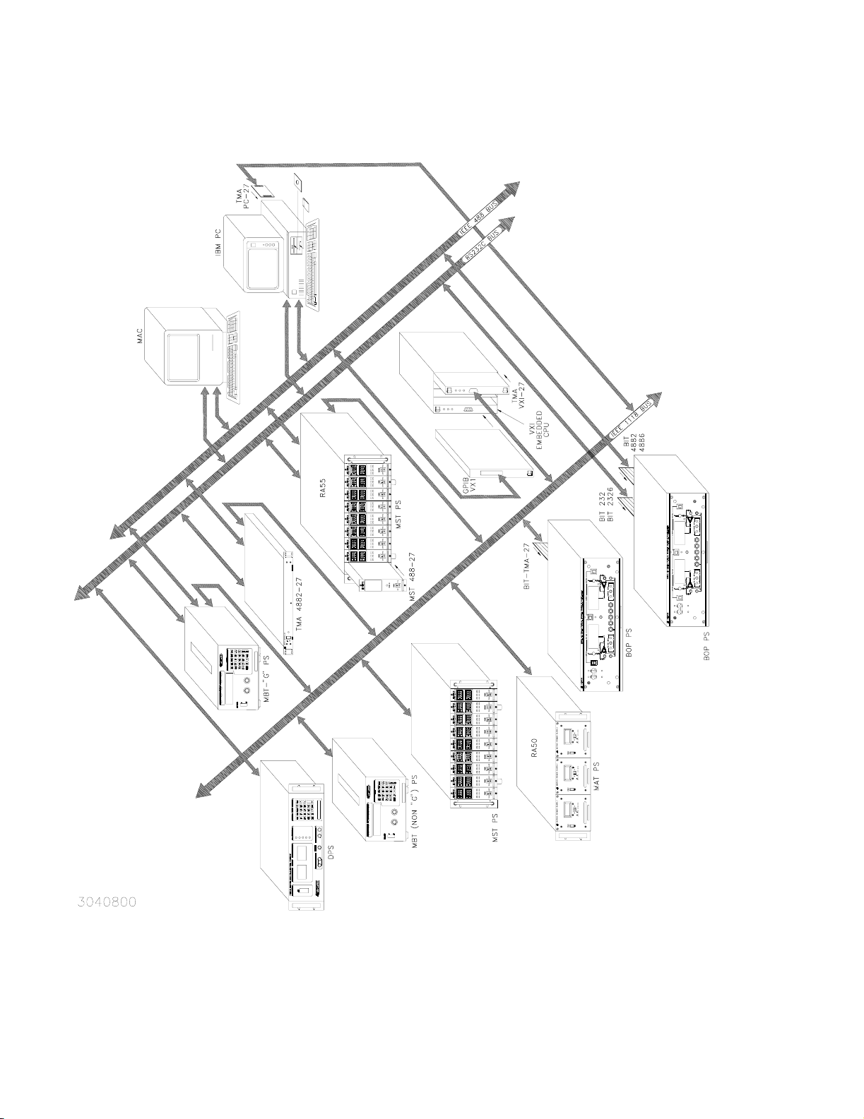
FIGURE 1-1. REMOTELY CONTROLLED POWER SUPPLY CONFIGURATIONS USING KEPCO PRODUCTS
Page 11

SECTION 1 - INTRODUCTION
1.1 SCOPE OF MANUAL
This manual contains instructions for the installation, operation and maintenance of the BIT
4882, BIT 4882-F, and BIT 4886 Interface Cards manufactured by Kepco, Inc., Flushing, NY,
U.S.A. References to "Interface Card" refer to both models.
1.2 GENERAL DESCRIPTION
The Kepco BIT Card Series were designed as an accessory for the Kepco BOP series bipolar
power supplies. The BIT cards make it possible to control the BOP output by means of digital
input signals (see Figure 1-1). The BIT card acts as an interface between the digital data bus
and the BOP, accepting the digital input data and converting it to an analog signal, which in
turn, controls the BOP output. The BIT 4882, BIT4882-F and BIT 4886 provide full talk/listen
capability. They are fully compliant with SCPI and CIIL high level programming languages.
The BIT 488 design group consists of four models. Field installable interface cards carry the
prefix "BIT". BOP bipolar power supplies with an installed BIT interface card carry the suffixes
shown in Table 1-1.
TABLE 1-1. KEPCO BIT 488, BIT 4882, AND BIT 4886 DIGITAL PROGRAMMING CARDS
FIELD INSTALLABLE
PROGRAMMING
CARD MODEL
BIT 488-B -488-B BYTE-SERIAL
BIT 488-D -488-D BYTE-SERIAL
BIT 4882 (See Table 1-2)
BIT 4882-F (See Table 1-2)
BIT 4886 -4886 BYTE-SERIAL
BIT TMA-27 -TMA 2-WIRE-SERIAL
FACTO RY
INSTALLED
PROGRAMMING
CARD BOP SUFFIX
-4882 BYTE-SERIAL
INPUT CODING
Except for the installation procedures, the BIT 4882 and 4882-F cards are functionally identical. The BIT 4886 card is functionally identical to the BIT 4882 card are except that the BIT
4886 provides 16 bit resolution vs. 12 bit for the BIT 4882. The BIT 4882 and BIT 4886 cards
include a PC board mounted IEEE 488 connector used with the BOP Models indicated in
Table 1-2; the BIT 4882-F is an earlier version of the BIT 4882 which is compatible with most
BOP models, although it is intended for earlier BOP Models indicated in Table 1-2.
RESOLUTION
MAIN
CHANNEL
12 BITS
(BINARY)
3-DIGIT
(BCD)
12 BITS
(BINARY)
16 BITS
(BINARY)
12 BITS
(BINARY)
LIMIT
CHANNEL
8 BITS
(BINARY)
2-DIGIT
(BCD)
12 BITS
(BINARY)
16 BITS
(BINARY)
12 BITS
(BINARY)
REMARKS
FOR THE
IEEE-488
OR GPIB BUIS
KEPCO
CONTROL BUS
BIT 4882 SVC 030507 1-1
Page 12

TABLE 1-2. APPLICABILITY OF BIT 4882, 4882-F AND BIT 4886 CARDS
TO SPECIFIC BOP MODELS
BOP TO BE MODIFIED
MODEL REVISION NO. MODEL REVISION NO.
1 BIT 4882-F
20-5M
2 AND LATER BIT 4882 10 AND LATER BIT 4882
12 TO 16 BIT 4882-F
20-10M
17 AND LATER BIT 4882 10 AND LATER BIT 4882
8 TO 14 BIT 4882-F
20-20M
15 AND LATER BIT 4882 14 AND LATER BIT 4882
12 TO 18 BIT 4882-F
36-6M
19 AND LATER BIT 4882 24 AND LATER BIT 4882
7 TO 12 BIT 4882-F
36-12M
13 AND LATER BIT 4882 15 AND LATER BIT 4882
16 TO 20 BIT 4882-F
50-2M
21 AND LATER BIT 4882 14 AND LATER BIT 4882
6 TO 12 BIT 4882-F
50-4M
13 AND LATER BIT 4882 7 AND LATER BIT 4882
NOTE: For modification of BOP Models with revision numbers that do not appear in this table, contact Kepco for assistance.
APPLICABLE
CARD
BOP TO BE MODIFIED
4 TO 9 BIT 4882-F
50-8M
5 TO 9 BIT 4882-F
72 3M
7 TO 13 BIT 4882-F
72-6M
17 TO 23 BIT 4882-F
100-1M
10 TO 14 BIT 4882-F
100-2M
6 TO 13 BIT 4882-F
100-4M
6 AND EARLIER BIT 4882-F
200-1M
APPLICABLE
CARD
1.3 SPECIFICATIONS, BIT 4882, BIT 4882-F AND BIT 4886 (SEE TABLE 1-3)
TABLE 1-3. SPECIFICATIONS, BIT 4882, BIT 4882-F AND BIT 4886
SPECIFICATION DESCRIPTION
OUTPUT VOLTAGE (MAIN CHANNEL) 0 ± 10V
OUTPUT VOLTAGE (LIMIT CHANNEL) 0 to +10V
OUTPUT CURRENT (EACH CHANNEL) 0 to ± 2 mA max.
OUTPUT IMPEDANCE <0.05 ohms
TEMPERATURE COEFFICIENT
OPTICAL ISOLATION
DIGITAL INPUT FORMAT Byte-Serial
POWER REQUIREMENT Supplied by BOP
PRGRAMMING RESOLUTION
DATA READBACK ACCURACY
VOLTAGE
CURRENT
VOLTAGE
CURRENT
Full scale: ± 35 ppm/°C max
Zero: ± 20µV/°C max
Digital and Analog grounds can be separated by a
maximum of 500 Volts.
RATING/DESCRIPTION CONDITION
0.024% 12 Bits
BIT 4882, 4882-F: 0.1%
BIT 4886: 0.2%
% of Max. Voltage
or Max. Current
1-2 BIT 4882 SVC 030507
Page 13

SECTION 2 - INSTALLATION
2.1 UNPACKING AND INSPECTION
The Interface Card has been thoroughly inspected and tested prior to packing and is ready for
operation following installation. Unpack, saving original packing material. If any indication of
damage is found, file a claim immediately with the responsible transport service.
2.2 SET START-UP DEFAULTS (SEE FIGURE 2-1)
Start-up defaults, consisting of Device Address, Language, IEEE Cable Shield Ground State,
and Power Supply Identification are initially set by means of DIP switches as described in the
following paragraphs.
2.2.1 SET (GPIB) DEVICE ADDRESS (SEE FIGURE 2-1)
The Device Address for the interface card is initially set by means of DIP switch S1, positions 1
through 5 (Figure 2-1). The Device Address is the permanent Listener or Talker address of the
interface card on the GPIB. It is factory preset to address 6. If a different Device Address is
required in your system, proceed as follows. There are 31 (0-30) possible choices (See Table 2-
1).
1. Position the Interface Card as depicted in Figure 2-1.
2. The Device Address DIP switches are positions 1 through 5 (from bottom to top, Figure 2-
1). These switches are preset by Kepco to address 6. For other device addresses set them
according to Table 2-1.
2.2.2 START-UP LANGUAGE DEFAULT (SEE FIGURE 2-1)
DIP switch S1 position 6 sets the Start-up Language Default:
• 0 = SCPI (factory default)
• 1 = CIIL
2.2.3 IEEE CABLE SHIELD GROUND SELECTION (SEE FIGURE 2-1)
The interface card is shipped from the factory configured so that the IEEE cable shield will be
grounded to the BOP chassis. In some cases, however, it may be desirable to break this connection to eliminate system “ground loops.” DIP switch S1 position 7 sets the Shield Ground
state:
• 0 = shield grounded (factory default)
• 1 = shield not grounded
2.2.4 SET POWER SUPPLY IDENTIFICATION SWITCH (SEE FIGURE 2-1)
Power Supply Identification switch S2 (Figure 2-1) identifies the BOP model to be controlled by
the interface card. Set Switch S2 positions 1 through 6 in accordance with Table 2-2.
BIT 4882 030507 2-1
Page 14
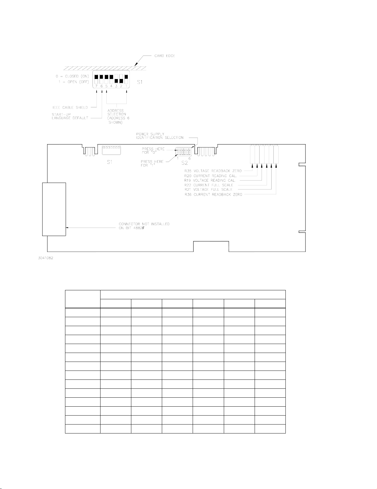
FIGURE 2-1. BIT 4882 AND BIT 4882-F SWITCH AND ADJUSTMENT LOCATIONS
TABLE 2-1. POWER SUPPLY IDENTIFICATION SWITCH S2 SETTING
MODEL
BOP 50-2M000000
100-1M 100000
20-10M010000
36-6M110000
50-4M001000
72-3M101000
100-2M 011000
20-20M111000
36-12M000100
50-8M100100
72-6M010100
100-4M 110100
200-1M 101100
20-5M011100
SW#1 SW#2 SW#3 SW#4 SW#5 SW#6
SELECTOR SWITCH S2 SECTION
2-2 BIT 4882 030507
Page 15

2.3 INSTALLATION OF INTERFACE CARD INTO THE BOP
• Refer to Figure 2-2 to install the BIT 4882-F interface card.
• Refer to Figure 2-3 to install the BIT 4882 or BIT 4886 interface card.
TABLE 2-2. DEVICE ADDRESS SELECTION
DECIMAL
ADDRESS
000000
100001
200010
300011
400100
500101
600110
700111
801000
901001
1001010
1101011
1201100
1301101
1401110
1501111
1610000
1710001
1810010
1910011
2010100
2110101
2210110
2310111
2411000
2511001
2611010
2711011
2811100
2911101
3011110
A5 A4 A3 A2 A1
SELECTOR SWITCH S1 SECTION
(SIGNAL LINE)
BIT 4882 030507 2-3
Page 16

NOTE: Step numbers coincide with encircled numbers on Figure 2-2, sheet 2.
Step 1. Remove a-c power to BOP by disconnecting line cord.
Step 2. Remove BOP cover (see Section 5, Figure 5-1 of your BOP Instruction Manual).
Step 3. Remove and discard Rear Cover Plate (PN 128-1434) and associated hardware.
Step 4. Remove J204 Connector Assembly (PN 241-0680) from Location #1, save for Step 9.
Step 5. Locate Transformer T202 and unplug connector from Location #4 only.
Step 6. Locate Rear Bracket and note part number (stamped on outside left edge):
if not PN 128-1810, contact Kepco.
Step 7. Unpack the BIT 4882-F Interface Card Installation Components (Transformer, PCB
Assembly, Cables #1 and #2, Connector Assembly, three (3) Knurled Nuts, five (5) washers, Spacer and Bracket).
Step 8. Install PCB Assembly (PN 235-1166) into the guides, slide into position so that mounting
holes in PCB Assembly line up with the three mounting posts on the BOP mounting
bracket.
Step 9. Secure the BIT 4882-F Interface Card to the Mounting Posts using the Knurled Nuts and
Lockwashers. Mount Connector J204 (Ref. Step 4, above) into Location #3 using the Lockwashers, Hex Spacer and Knurled Nut.
Step 10. Install Cable #1 (18-position connectors) to the BIT 4882-F Interface Card; mate the other
end of the cable with Location #1 on BOP A1 Assembly.
Step 11. Install Cable #2 (5-position connectors) to the BIT 4882-F Interface Card; mate the other
end of the cable with Location #2 on BOP A1 Assembly.
Step 12. Plug in 3-pin connector (Ref. Step 5, above) from Transformer 100-2354 as shown.
Step 13. Plug in Ribbon Cable Assembly 195-0085 as shown. Secure ribbon cable connector to
chassis using knurled nut.
Step 14. Mark "-4882" after Model No. on Nameplate (see Detail A).
Step 15. Remove "Control Identification" label (PN 188-1107) and "Address Label" (PN 188-1012).
Affix revised "Control Identification" label (PN 188-1445) and "Address Label" (PN
188-1726) in vacated positions (with part numbers facing front panel).
Step 16. Reinstall BOP cover.
Step 17. Perform calibration procedure detailed in Section 3 of this manual.
FIGURE 2-2. INSTALLATION OF MODEL BIT 4882-F INTO BOP (SHEET 1 OF 2)
2-4 BIT 4882 030507
Page 17

FIGURE 2-2. INSTALLATION OF MODEL BIT 4882-F INTO BOP (SHEET 2 OF 2).
BIT 4882 030507 2-5
Page 18

NOTE: Step numbers coincide with encircled numbers on Figure 2-3, sheet 2.
Step 1. Remove a-c power to BOP by disconnecting line cord.
Step 2. Remove BOP cover (see Section 5, Figure 5-1 of your BOP Instruction Manual).
Step 3. Remove and discard Rear Cover Plate (PN 128-1434) and associated hardware.
Step 4. Remove J204 Connector Assembly (PN 241-0680) from Location #1, save for Step 9.
Step 5. Locate Transformer T202 and unplug connector from Location #4 only.
Step 6. Locate Rear Bracket and note part number (stamped on outside left edge):
if not PN 128-1810, contact Kepco.
Step 7. Unpack the BIT 4882 Interface Card Installation Components (PCB Assembly, Cables #1 and
#2, Connector Assembly, three (3) Knurled Nuts, five (5) washers, Spacer and Bracket).
Step 8. Install PCB Assembly (PN 235-1166) into the guides, slide into position so that mounting holes
in PCB Assembly line up with the three mounting posts on the BOP mounting bracket.
Step 9. Secure the BIT 4882 Interface Card to the Mounting Posts using the Knurled Nuts and Lock-
washers. Mount Connector J204 (Ref. Step 4, above) into Location #3 using the Lockwashers,
Hex Spacer and knurled nut.
Step 10. Install Cable #1 (18-position connectors) to the BIT 4882 Interface Card, mate the other end of
the cable with Location #1 on BOP A1 Assembly.
Step 11. Install Cable #2 (5-position connectors) to the BIT 4882 Interface Card, mate the other end of
the cable with Location #2 on BOP A1 Assembly.
Step 12. Plug in 3-pin connector (Ref. Step 5, above) from Transformer 100-2354 as shown.
Step 13. Mark "-4882” after Model No. on Nameplate (see Detail A).
Step 14. Remove "Control Identification" label (PN 188-1107) and "Address Label" (PN 188-1012). Affix
revised "Control Identification" label (PN 188-1445) and "Address Label" (PN 188-1726) in
vacated positions (with part numbers facing front panel).
Step 15. Reinstall BOP cover.
Step 16. Perform calibration procedure detailed in Section 3 of this manual.
FIGURE 2-3. INSTALLATION OF MODEL BIT 4882 INTO BOP (SHEET 1 OF 2)
2-6 BIT 4882 030507
Page 19

FIGURE 2-3. INSTALLATION OF MODEL BIT 4882 INTO BOP (SHEET 2 OF 2).
BIT 4882 030507 2-7
Page 20

2.4 INPUT/OUTPUT SIGNALS
The IEEE 488 port is a 24 pin IEEE 488 connector (Figure 2-4) and conforms mechanically and
electrically to the IEEE 488 standard. Refer to Table 2-3 for pin assignments.
TABLE 2-3. INPUT/OUTPUT PIN ASSIGNMENTS
PIN SIGNAL NAME FUNCTION
1
2
3
4
5 EOI End or Identify
6 D AV Da t a Valid
7 NRFD Not Ready for Data
8 NDAC Not Data Accepted
9 IFC Interface Clear
10 SRQ Service Request
11 ATN Attention
12 SHIELD Shield
13
14
15
16
17 REN Remote Enable
18 GND Ground (signal common)
19 GND Ground (signal common)
20 GND Ground (signal common)
21 GND Ground (signal common)
22 GND Ground (signal common)
23 GND Ground (signal common)
24 LOGIC GND Logic Ground
I01
D
I02
D
I03
D
I04
D
I05
D
DI06
DI07
DI08
I/O Line
I/O Line
I/O Line
I/O Line
I/O Line
I/O Line
I/O Line
I/O Line
FIGURE 2-4. IEEE 488 (GPIB) CONNECTOR
2-8 BIT 4882 030507
Page 21

SECTION 3 - CALIBRATION
NOTE: The calibration procedures below are for the purpose of recalibration and for the case
where the BIT card is installed by the user. Unless otherwise noted, syntax is in SCPI.
3.1 EQUIPMENT REQUIRED
The following is a listing of equipment required for calibration of the Interface Card installed in a
Kepco “BOP” Series Power Supply:
A. Precision digital voltmeter (DVM), 5 digit minimum resolution (suggested).
B. An IEEE 488 System Controller, (with appropriate software) connected to BOP Power Sup-
ply with an IEEE 488 cable.
C. Precision four-terminal current shunt (with suitable power rating and tolerance for the cur-
rents to be measured).
3.2 ADJUSTMENT OF THE BOP ±10 VOLT CALIBRATION CONTROLS (R31, R32)
NOTE: BOP cover removal required for this step.
1. Connect a DVM to the REAR PROGRAMMING CONNECTOR (PC-12); between common
and pin 28 (+10Vdc REFERENCE).
2. Turn the BOP Power Supply “ON” and locate the calibration controls (see Figure 3-1, refer to
Table 3-1). Adjust R31 for +10.000Vdc.
3. Turn the BOP Power Supply “OFF” and connect DVM between common and pin 22 (–10Vdc
REFERENCE).
4. Turn the BOP Power Supply “ON”. Adjust R32 for –10.000Vdc.
5. Turn the BOP Power Supply “OFF”.
3.3 ADJUSTMENT OF THE AMMETER ZERO (R50)
1. Without a load connected to the BOP output, connect the DVM to the REAR PROGRAMMING CONNECTOR (PC-12); between COMMON and pin 10.
2. Turn the BOP Power Supply “ON” and locate AMMETER ZERO control R50 (see Figure 3-1,
refer to Table 3-1).
3. Adjust the control for zero, ±100 microvolts.
4. Turn the BOP Power Supply “OFF”.
BIT 4882 030507 3-1
Page 22

FIGURE 3-1. BOP POWER SUPPLY, INTERNAL CALIBRATION CONTROL LOCATIONS
3.4 ADJUSTMENT OF THE OUTPUT VOLTAGE ZERO (R81)
1. Without a load connected to the BOP output, connect a DVM between the FRONT PANEL
SENSING TERMINALS of the BOP Power Supply.
2. Turn the BOP Power Supply “ON”, program the BOP Power Supply to ZERO VOLTAGE
AND MAXIMUM CURRENT LIMIT.
• If using SCPI send VOLT 0;CURR MAX
• If using CIIL send FNC DCS:CH1 VOLT 0 with CURL .5
3. Locate Eo COMP AMP ZERO control R81 (see Figure 3-1, refer to Table 3-1).
4. Adjust control R81 for zero, ±100 microvolts.
3.5 ADJUSTMENT OF THE FULL SCALE OUTPUT VOLTAGE (R21)
1. Program the BOP Power Supply for PLUS FULL SCALE VOLTAGE.
• If using SCPI send VOLT MAX;CURR MAX
• If using CIIL send FNC DCS:CH1 VOLT xx with CURL .5
where xx is the maximum rated output voltage of the BOP.
3-2
BIT 4882 100203
Page 23

2. MEASURE the output voltage at the sense terminals at the BOP front panel using the DVM.
3. Locate VOLTAGE FULL SCALE control R21 (see Figures 2-1 and 3-1, refer to Table 3-1).
4. Adjust control R21 as needed until DVM reads FULL SCALE VOLTAGE, ±1 millivolt.
TABLE 3-1. BOP POWER SUPPLY, INTERNAL CALIBRATION CONTROLS
REFERENCE
DESIGNATION
R19 * VOLTAGE READING ‘MEASURE’d voltage reading adjustment 3.7
R20 * CURRENT READING ‘MEASURE’d current reading adjustment 3.11
R21 * VOLTAGE FULL SCALE Full scale output voltage adjustment 3.5
R22 * CURRENT FULL SCALE Full scale output current adjustment 3.9
A1R31, A1R32 ( ± ) 10V CAL. Reference voltage calibration 3.2
R35 * VOLTAGE READBACK ZERO Zero output voltage readback adjustment 3.6
R36 * CURRENT READBACK ZERO Zero output current readback adjustment 3.10
R50 * AMMETER ZERO Sensing amplifier offset adjustment 3.3
A1R81
A1R83
* Located on BIT 4882 card
CONTROL
NAME
EO COMP AMP ZERO Voltage channel zero adjustment
IO COMP AMP ZERO Current channel zero adjustment
PURPOSE
ADJUSTMENT
PROCEDURE
3.6 VOLTAGE READING ZERO CALIBRATION (R35)
1. Program the BOP power supply for ZERO VOLTAGE and MAXIMUM CURRENT LIMIT.
(PAR.)
3.4
3.8
• If using SCPI send VOLT 0;CURR MAX
• If using CIIL send FNC DCS:CH1 VOLT 0 with CURL .5
BIT 4882 030507 3-3
Page 24

2. MEASURE the output voltage using programming commands, then check the readback
data.
• In SCPI send MEAS:VOLT?
• In CIIL: send FNC DCS:CH1 GAL
F0
INX VOLT
FTH VOLT
NOTE: For subsequent measurements using CIIL it is only necessary to send INX
VOLT and FTH VOLT commands.
3. Locate VOLTAGE READBACK ZERO control R35 (see Figures 2-1 and 3-1, refer to Table 3-
1).
4. Adjust control R35 until the readback value is not 0.0 using MEASURE commands (see step
2) as needed.
5. Adjust control R35 (opposite direction from step 4 above) until the readback value is 0.0
using MEASURE commands (see step 2) as needed. Once a stable value of 0.0 is reached,
continue rotating R35 four full (360°) turns in the same direction. Verify readback voltage is
0.0 using MEASURE commands (see step 2) as needed.
3.7 VOLTAGE READING CALIBRATION (R19)
1. Program the BOP power supply for PLUS FULL SCALE VOLTAGE, less one percent, e.g.,
for a 20V unit, program BOP to 19.8V (verify by reading external DVM).
• If using SCPI send VOLT yy;CURR MAX
• If using CIIL send FNC DCS:CH1 VOLT yy with CURL .5
where yy is the maximum rated output voltage of the BOP less one percent.
2. MEASURE the output voltage using programming commands, then check the readback
data.
• In SCPI send MEAS:VOLT?
• In CIIL: send FNC DCS:CH1 GAL
F0
INX VOLT
FTH VOLT
NOTE: For subsequent measurements using CIIL it is only necessary to send INX
VOLT and FTH VOLT commands.
3. Locate VOLTAGE READ. CAL. control R19 (see Figures 2-1 and 3-1, refer to Table 3-1).
4. Adjust control R19 until the readback value matches the programmed value using MEASURE commands (see step 2) as needed.
5. Turn the BOP Power Supply “OFF”.
3.8 ADJUSTMENT OF THE OUTPUT CURRENT ZERO (R83)
1. With the BOP Power Supply “OFF”, connect a precision current shunt (R
FRONT PANEL OUTPUT TERMINALS.
) between the
S
2. Connect the DVM to the other two terminals of the precision shunt as shown in Figure 3-2.
3-4 BIT 4882 030507
Page 25

3. Turn the BOP “ON” and program the BOP Power Supply to ZERO CURRENT and MAXIMUM VOLTAGE LIMIT.
• If using SCPI send FUNC:MODE CURR;:CURR 0;VOLT MAX
• If using CIIL send FNC DCS:CH1 CURR 0 with VLTL 20
4. Locate Io COMP AMP ZERO control R83 (see Figure 3-1, refer to Table 3-1).
5. Adjust control R83 for zero, per Table 3-2, OUTPUT CURRENT ZERO.
6. Turn the BOP Power Supply “OFF”.
3.9 ADJUSTMENT OF THE FULL SCALE OUTPUT CURRENT (R22)
1. With the BOP Power Supply “OFF”, connect the PRECISION 4-TERMINAL SHUNT to the
power supply output terminals and connect the DVM to the PRECISION 4-TERMINAL
SHUNT (see Figure 3-2)
2. Turn the BOP Power Supply “ON” and program the BOP Power Supply for PLUS FULL
SCALE CURRENT and MAXIMUM VOLTAGE LIMIT.
• If using SCPI send FUNC:MODE CURR;:CURR MAX;VOLT MAX
• If using CIIL send FNC DCS:CH1 CURR zz with VLTL 20
where zz is the maximum rated output current of the BOP.
3. Locate CURRENT FULL SCALE control R22 (see Figures 2-1 and 3-1, refer to Table 3-1).
4. MEASURE the output current using the DVM. Adjust control R22 as needed until DVM reads
exactly FULL SCALE CURRENT per Table 3-2, FULL SCALE CURRENT ACCURACY.
3.10 CURRENT READING ZERO CALIBRATION (R36)
NOTE: The Output Current Zero Adjustment (PAR. 3.8) must be done before performing the fol-
lowing procedure, and the PRECISION 4-TERMINAL SHUNT should be still connected
to the power supply output terminals.
1. Program the BOP Power Supply for ZERO CURRENT and MAXIMUM VOLTAGE LIMIT.
• If using SCPI send FUNC:MODE CURR;:CURR 0;VOLT MAX
• If using CIIL send FNC DCS:CH1 CURR 0 with VLTL 20
2. MEASURE the output current using programming commands, then check the readback
data.
• In SCPI send MEAS:CURR? then check the readback data.
• In CIIL: send FNC DCS:CH1 GAL
F0
INX CURR
FTH CURR
NOTE: For subsequent measurements using CIIL it is only necessary to send INX
CURR and FTH CURR commands.
3. Locate CURRENT READBACK ZERO control R36 (see Figures 2-1 and 3-1, refer to Table
3-1).
4. Adjust control R36 until the readback value is not 0.0 using MEASURE commands (see step
2) as needed.
BIT 4882 030507 3-5
Page 26

5. Adjust control R36 (opposite direction from step 4 above) until the readback value is 0.0
using MEASURE commands (see step 2) as needed. Once a stable value of 0.0 is reached,
continue rotating R36 four full (360°) turns in the same direction. Verify readback current is
0.0 using MEASURE commands (see step 2) as needed.
TABLE 3-2. CALIBRATION MEASUREMENTS AND TOLERANCES - CURRENT
MODEL
BOP 100-1M
BOP 200-1M
BOP 50-2M
BOP 100-2M
BOP 72-3M 1 Ohm
BOP 50-4
BOP 100-4M
BOP 20-5M 0.1 Ohm
BOP 36-6M
BOP 72-6M
BOP 50-8 0.1 Ohm
BOP 20-10M 0.1 Ohm
BOP 36-12M
BOP 20-20M
REFER TO NOTES IF EXACT
SENSE RESISTOR VALUE IS
KNOWN.
USE SPACE PROVIDED AT
RIGHT FOR CALCULATED
VALUES.
SENSE RESISTOR VALUE
(SEE NOTES AND TABLE 3-3)
1 Ohm
1 Ohm
1 Ohm
0.1 Ohm
0.1 Ohm
0.01 Ohm
R
SENSE
SEE
NOTE.
OUTPUT
CURRENT
ZERO
0V
±0.000025V
0V
±0.00005V
0V
±0.000075V
0V
±0.0001V
0V
±0.0000125V
0V
±0.000015V
0V
±0.00002V
0V
±0.000025V
0V
±0.00003V
0V
±0.0000005V
SEE
NOTE A.
FULL SCALE
CURRENT
ACCURACY
1V (MAX)
-1V (MIN)
±0.000150V
2V (MAX)
-2V (MIN)
±0.00030V
3V (MAX)
-3V (MIN)
±0.0006V
4V (MAX)
-4V (MIN)
±0.0008V
0.5V (MAX)
-0.5V (MIN)
±0.0000750V
0.6V (MAX)
-0.6V (MIN)
±0.000090V
0.8V (MAX)
-0.8V (MIN)
±0.00012V
1.0V (MAX)
-1.0V (MIN)
±0.000150V
1.2V (MAX)
-1.2V (MIN)
±0.00018V
0.2V (MAX)
-0.2V (MIN)
±0.0000030V
SEE NOTES C AND
D
NOTES: The following formula is used to calculate proper calibration values if the exact Sense Resistor value is
known.
R
= the measured value of the sense resistor to 6 places (minimum).
SENSE
I = Rated current output of BOP (e.g., for BOP 50-4M, I = 4)
(
R
SENSE
) (I) (0.00075) [FOR MODELS WHERE I = 3 OR 4 USE (
R
) (I) (0.00012)]
SENSE
3-6 BIT 4882 030507
Page 27

TABLE 3-3. SUGGESTED SENSE RESISTORS
VALUE KEPCO PART NO. MANUFACTURER MANUFACTURER PART NO.
0.01 OHM 115-2997 ISOTEK RUG-Z-R010-0.1 TK10
0.1 OHM 115-2995 ISOTEK RUG-Z-R100-0.1 TK10
1 OHM 115-2996 ISOTEK RUG-Z-1R00-0.1 TK10
NOTE: ALL SENSE RESISTORS MUST BE MOUNTED ON A HEATSINK WITH A MINIMUM SURFACE AREA OF
36 SQUARE INCHES TO MAINTAIN THERMAL STABILITY DURING CALIBRATION.
FIGURE 3-2. CURRENT SHUNT CONNECTIONS
BIT 4882 030507 3-7
Page 28

3.11 CURRENT READING CALIBRATION (R20)
NOTE: The Full Scale Output Current Adjustment (PAR. 3.9) must be done before performing
the following procedure, and the PRECISION 4-TERMINAL SHUNT should be still
connected to the power supply output terminals.
1. Program the BOP Power Supply for PLUS FULL SCALE CURRENT, less one percent (verify
by reading external DVM). E.g., for 20V
• If using SCPI send FUNC:MODE CURR;:CURR zz;VOLT MAX
• If using CIIL send FNC DCS:CH1 CURR zz with VLTL 20
where zz = aa - (aa/100) where aa is the maximum rated output current of the
BOP (e.g., for BOP 20-10M, zz = 10-(10/100) = 9.9).
2. MEASURE the output current using programming commands, then check the readback
data.
• In SCPI send MEAS:CURR? then check the readback data.
• In CIIL: send FNC DCS:CH1 GAL
F0
INX CURR
FTH CURR
NOTE: For subsequent measurements using CIIL it is only necessary to send INX
CURR and FTH CURR commands.
3. Locate CURRENT READ. CAL. control R20 (see Figures 2-1 and 3-1, refer to Table 3-1).
4. Adjust control R20, until the measured value matches the programmed value using MEASURE commands (see step 2) as needed.
3-8 BIT 4882 030507
Page 29

SECTION 4 - OPERATION
4.1 GENERAL
The Kepco BOP Power Supply, with an installed BIT 4882, BIT 4882-F or BIT 4886 Interface
Card, may be programmed over the IEEE 488 standard communication bus (General Purpose
Interface Bus, GPIB) using either SCPI (Standard Commands for Programmable Instruments)
or CIIL (Control Interface Intermediate Language) commands. SCPI and CIIL provide a common language used in an automatic test system. (Refer to Table 2-3 for input/output signal allocations.)
4.2 IEEE 488 (GPIB) BUS PROTOCOL
Table 4-1 defines the interface capabilities of the Interface Card (Talker/Listener) relative to the
IEEE 488 (GPIB) bus (reference document ANSI/IEEE Std 488: IEEE Standard Digital Interface for
Programmable Instrumentation) communicating with a Host Computer–Controller (Talker/Listener).
TABLE 4-1. IEEE 488 (GPIB) BUS INTERFACE FUNCTIONS
FUNCTION
Source Handshake SH1 Complete Capability (Interface can receive multiline messages)
Acceptor Handshake AH1 Complete Capability (Interface can receive multiline messages)
Ta lk er T 6
Listener L4 Basic listener, unaddress if MTA (My Talk Address) (one-byte address).
Service Request SR1
Remote/Local RL2 No Local lock-out.
Parallel Poll PP0 No Capability
Device Clear DC1
Device Trigger DT1 Complete Capability
Controller C0 No Capability
SUBSET
SYMBOL
Basic talker, serial poll, unaddress if MLA (My Listen Address) (one-byte
address)
Complete Capability. The interface sets the SRQ line true if there is an
enabled service request condition.
Complete Capability. Controller sends DCL (Device Clear) and SDC
(Selected Device Clear) to selected power supply.
COMMENTS
Tables 4-2 and 4-3 define the messages sent to the Interface Card, or received by the Interface
Card, via the IEEE 488 bus in IEEE 488 command mode and IEEE 488 data mode, respectively. These messages are enabled during the “handshake” cycle, with the Interface Card operating as either a Talker or a Listener.
BIT 4882 030507 4-1
Page 30

TABLE 4-2. IEEE 488 (GPIB) BUS COMMAND MODE MESSAGES
MNEMONIC MESSAGE DESCRIPTION COMMENTS
ATN Attention Received
DAC Data accepted Received or Sent
DAV Data Valid Received or Sent
DCL Device Clear Received
GET Group Executive Trigger Received
IFC Interface Clear Received
MLA My Listen Address Received
MTA My Talk Address Received
OTA Other Talk Address Received
RFD Ready for Data Received or Sent
SDC Selected Device Clear Received
SPD Serial Poll Disable Received
SPE Serial Poll Enable Received
SRQ Service Request Sent
UNL Unlisten Received
UNT Untalk Received
TABLE 4-3. IEEE 488 (GPIB) BUS DATA MODE MESSAGES
MNEMONIC MESSAGE DESCRIPTION COMMENTS
DAB
END
EOS
RQS
STB
4.3 SCPI PROGRAMMING
SCPI (Standard Commands for Programmable Instruments) is a programming language conforming to the protocols and standards established by IEEE 488.2 (reference document ANSI/
IEEE Std 488.2, IEEE Standard Codes, Formats, Protocols, and Common Commands). SCPI commands are sent to the Interface Card as output strings within the selected programming language (PASCAL, BASIC, etc.) in accordance with the manufacturer’s requirements for the
particular GPIB interface card used.
Data Byte Received or Sent
End Received or Sent
End of String Received or Sent
Request Service Sent
Status Byte Sent
4-2 BIT 4882 030507
Page 31

Different programming languages (e.g., BASIC, C, PASCAL, etc.) have different ways of representing data that is to be put on the IEEE 488 bus. It is up to the programmer to determine how
to output the character sequence required for the programming language used. Address information (GPIB address) must be included before the command sequence. (See PAR. 2.2.1 to
establish the Interface Card GPIB address.)
4.3.1 SCPI MESSAGES
There are two kinds of SCPI messages: program messages from controller to power supply,
and response messages from the power supply to the controller. Program messages consist of
one or more properly formatted commands/queries and instruct the power supply to perform an
action; the controller may send a program message at any time. Response messages consist of
formatted data; the data can contain information regarding operating parameters, power supply
state, status, or error conditions.
4.3.2 COMMON COMMANDS/QUERIES
Common commands and queries are defined by the IEEE 488.2 standard to perform overall
power supply functions (such as identification, status, or synchronization) unrelated to specific
power supply operation (such as setting voltage/current). Common commands and queries are
preceded by an asterisk (*) and are defined and explained in Appendix A (see Table 4-4). Refer
also to syntax considerations (PARs 3.4.3 through 3.4.6).
4.3.3 SCPI SUBSYSTEM COMMAND/QUERY STRUCTURE
Subsystem commands/queries are related to specific power supply functions (such as setting
output voltage, current limit, etc.) Figure 4-1 is a tree diagram illustrating the structure of SCPI
subsystem commands used in the Interface Card with the “root” at the left side, and specific
commands forming the branches. The subsystem commands are defined and explained in
Appendix B (see Table 4-4).
ROOT : (colon)
INITiate
[:IMMediate]
:CONTinuous
MEASure
:CURRent?
:VOLTage?
[SOURce:]
VOLTage
[:LEVel]
[:IMMediate]
:TRIGgered
CURRent
[:LEVel]
[:IMMediate]
:TRIGgered
FUNCtion
:MODE
STATus
:OPERation
:CONDition?
:ENABle
[:EVENt]?
:PRESet
:QUEStionable
:CONDition?
:ENABle
[:EVENt]?
SYSTem
:ERRor?
:LANGuage
FIGURE 4-1. TREE DIAGRAM OF SCPI COMMANDS USED WITH BIT 4882, BIT 4882-F
AND BIT 4886 INTERFACE CARD
BIT 4882 030507 4-3
Page 32

4.3.4 PROGRAM MESSAGE STRUCTURE
SCPI program messages (commands from controller to power supply) consist of one or more
message units ending in a message terminator (required by Kepco power modules). The message
terminator is not part of the syntax; it is defined by the way your programming language indicates the end of a line (such as a “newline” or “end-of-line” character). The message unit is a
keyword consisting of a single command or query word followed by a message terminator (e.g.,
CURR?<newline> or TRIG<end-of-line>). The message unit may include a data parameter after
the keyword separated by a space; the parameter is usually numeric (e.g., CURR 5<newline>),
but may also be a string (e.g., OUTP ON<newline>). Figure 4-2 illustrates the message structure, showing how message units are combined. The following subparagraphs explain each
component of the message structure.
NOTE: An alternative to using the message structure for multiple messages defined in the fol-
lowing paragraphs is to send each command as a separate line. In this case each
command must use the full syntax shown in Appendix B.
TABLE 4-4. SCPI COMMAND INDEX
COMMAND PAGE COMMAND PAGE
*CLS A-1 [SOUR]:CURR? B-5
*ESE A-2 [SOUR]:CURR:TRIG B-6
*ESE? A-2 [SOUR]:CURR:TRIG? B-6
*ESR? A-3 [SOUR]:VOLT B-7
*IDN? A-3 [SOUR]:VOLT? B-7
*OPC A-4 [SOUR]:VOLT:TRIG B-8
OPC? A-4 [SOUR]:VOLT:TRIG? B-8
*RST A-5 [SOUR]:FUNC:MODE B-9
*SRE A-6 STAT:OPER:COND? B-9
*SRE? A-6 STAT:OPER:ENAB B-10
*STB? A-7 STAT:OPER:ENAB? B-10
*TRG A-7 STAT:OPER? B-11
*TST A-8 STAT:PRES B-11
*WAI A-8 STAT:QUES? B-12
INIT[:IMM] B-1 STAT:QUES:COND? B-12
INIT:CONT B-1 STAT:QUES:ENAB B-13
INIT:CONT? B-2 STAT:QUES:ENAB? B-13
MEAS:CURR? B-3 SYST:ERR? B-14
MEAS:VOLT? B-3 SYST:LANG B-14
[SOUR]:CURR B-4
4-4 BIT 4882 030507
Page 33

4.3.4.1 KEYWORD
Keywords are instructions recognized by a decoder within the Interface Card, referred to as a
“parser.” Each keyword describes a command function; all keywords used by the Interface Card
are listed in Figure 4-1.
Each keyword has a long form and a short form. For the long form the word is spelled out completely (e.g. STATUS, OUTPUT, VOLTAGE, and TRIGGER are long form keywords). For the
short form only the first three or four letters of the long form are used (e.g., STAT, VOLT, OUTP,
and TRIG). The rules governing short form keywords are presented in Table 4-5.
TABLE 4-5. RULES GOVERNING SHORTFORM KEYWORDS
IF NUMBER OF LETTERS IN
LONGFORM KEYWORD IS:
4 OR FEWER (DOES NOT MATTER) ALL LONG FORM LETTERS MODE
5 OR MORE
KEYWORD
ROOT SPECIFIER
MESSAGE UNIT SEPARATOR
DATA
DATA SEPARATOR
KEYWORD
AND FOURTH LETTER
IS A VOWEL?
NO
YES
THEN SHORT FORM
CONSISTS OF:
THE FIRST FOUR
LONG FORM LETTERS
THE FIRST THREE
LONG FORM LETTERS
DATA SEPARATOR
DATA
EXAMPLES
MEASure, OUTPut, EVENt
LEVel, IMMediate, ERRor
MESSAGE UNIT SEPARATOR
ROOT SPECIFIER
KEYWORD
KEYWORD SEPARATOR
KEYWORD
QUERY INDICATOR
MESSAGE TERMINATOR
CURR:LEV 3.5;:OUTP ON;:CURR?<NL>
MESSAGE UNIT
FIGURE 4-2. MESSAGE STRUCTURE
BIT 4882 030507 4-5
Page 34

You must use the rules above when using keywords. Using an arbitrary short form such as
ENABL for ENAB (ENABLE) or IMME for IMM (IMMEDIATE) will result in an error. Regardless
of which form chosen, you must include all the letters required by that form.
To identify the short form and long form in this manual, keywords are written in upper case letters to represent the short form, followed by lower case letters indicating the long form (e.g.,
IMMediate, EVENt, and OUTPut). The parser, however, is not sensitive to case (e.g., outp,
OutP, OUTPUt, ouTPut, or OUTp are all valid).
4.3.4.2 KEYWORD SEPARATOR
If a command has two or more keywords, adjacent keywords must be separated by a colon (:)
which acts as the keyword separator (e.g., CURR:LEV:TRIG). The colon can also act as a root
specifier (paragraph 3.4.4.7).
4.3.4.3 QUERY INDICATOR
The question mark (?) following a keyword is a query indicator. This changes the command into
a query. If there is more than one keyword in the command, the query indicator follows the last
keyword. (e.g., VOLT? and MEAS:CURR?).
4.3.4.4 DATA
Some commands require data to accompany the keyword either in the form of a numeric value
or character string. Data always follows the last keyword of a command or query (e.g.,
VOLT:LEV:TRIG 14 or SOUR:VOLT? MAX
4.3.4.5 DATA SEPARATOR
Data must be separated from the last keyword by a space (e.g., VOLT:LEV:TRIG 14 or
SOUR:VOLT? MAX
4.3.4.6 MESSAGE UNIT SEPARATOR
When two or more message units are combined in a program message, they must be separated
by a semicolon (;) (e.g., VOLT 15;MEAS:VOLT? and CURR 12; CURR:TRIG 12.5).
4.3.4.7 ROOT SPECIFIER
The root specifier is a colon (:) that precedes the first keyword of a program message. This
places the parser at the root (top left, Figure 4-3) of the command tree. Note the difference
between using the colon as a keyword separator and a root specifier in the following examples:
VOLT:LEV:IMM 16 Both colons are keyword separators.
:CURR:LEV:IMM 4 The first colon is the root specifier, the other two are keyword separators.
VOLT:LEV 6;:CURR:LEV 15 The second colon is the root specifier, the first and third are keyword separators
:INIT ON;:TRIG;:MEAS:CURR?;VOLT? The first three colons are root specifiers.
4-6 BIT 4882 030507
Page 35

4.3.4.8 MESSAGE TERMINATOR
The message terminator defines the end of a message. Three message terminators are permitted:
• new line (<NL>), ASCII 10 (decimal) or 0A (hex)
• (<CR>), ASCII 13 (decimal) or 0D (hex)
• both of the above (<CR> <NL>)
Your GPIB interface card software will automatically send a message terminator. For example,
the HP BASIC OUTPUT statement inserts <NL> after the last data byte. When binary data is
exchanged, <END> must be used. The combination <NL><END> terminator can be used for all
data except binary data.
NOTE: Kepco power modules require a message terminator at the end of each program mes-
sage. The examples shown in this manual assume a message terminator will be added
at the end of each message. Where a message terminator is shown it is represented
as <NL> regardless of the actual terminator character.
4.3.5 UNDERSTANDING THE COMMAND STRUCTURE
Understanding the command structure requires an understanding of the subsystem command
tree illustrated in Figure 4-3. The “root” is located at the top left corner of the diagram. The
parser goes to the root if:
• a message terminator is recognized by the parser
• a root specifier is recognized by the parser
Optional keywords are enclosed in brackets [ ] for identification; optional keywords can be omitted and the power supply will respond as if they were included in the message. The root level
keyword [SOURce] is an optional keyword. Starting at the root, there are various branches or
paths corresponding to the subsystems. The root keywords for the Interface Card are :INITiate,
:MEASure, :OUTPut, [:SOURce], :STATus, and :SYSTem. Because the [SOURce] keyword is
optional, the parser moves the path to the next level, so that VOLTage, CURRent, and FUNCtion commands are at the root level.
Each time the parser encounters a keyword separator, the parser moves to the next indented
level of the tree diagram. As an example, the STATus branch is a root level branch that has
three sub-branches: OPERation, PRESet, and QUEStionable. The following illustrates how
SCPI code is interpreted by the parser:
STAT:PRES<NL>
The parser returns to the root due to the message terminator.
STAT:OPER?;PRES<NL>
The parser moves one level in from STAT. The next command is expected at the level defined
by the colon in front of OPER?. Thus you can combine the following message units
STAT:OPER? and STAT:PRES;
STAT:OPER:COND?;ENAB 16<NL>
After the OPER:COND? message unit, the parser moves in one level from OPER, allowing the
abbreviated notation for STAT:OPER:ENAB.
BIT 4882 030507 4-7
Page 36

4.3.6 PROGRAM MESSAGE SYNTAX SUMMARY
• Common commands begin with an asterisk (*).
• Queries end with a question mark (?).
• Program messages consist of a root keyword and, in some cases, one or more message
units separated by a colon (:) followed by a message terminator. Several message units
of a program message may be separated by a semicolon (;) without repeating the root
keyword.
• If a program message has more than one message unit, then a colon (:) must precede
the next keyword in order to set the parser back to the root (otherwise the next keyword
will be taken as a subunit of the previous message unit).
e.g., the command meas:volt?;curr? will read output voltage and output current
since both volt? and curr? are interpreted as subunits of the meas command.
• Several commands may be sent as one message; a line feed terminates the message.
Commands sent together are separated by a semicolon (;). The first command in a message starts at the root, therefor a colon (:) at the beginning is not mandatory.
e.g., the command meas:volt?;:curr? will read output voltage and programmed
current since the colon preceding curr? indicates that curr? is not part of the meas
command and starts at the root.
• UPPER case letters in mnemonics are mandatory (short form). Lower case letters may
either be omitted, or must be specified completely (long form)
e.g., INSTrument (long form) has the same effect as INST (short form).
• Commands/queries may be given in upper/lower case (long form)
e.g., SoUrCe is allowed.
• Text shown between brackets [] is optional.
e.g., :[SOUR]VOLT:[LEV] TRIG has the same effect as :VOLT TRIG
4.3.7 SCPI PROGRAM EXAMPLE
Figure 4-3 is an example of a program using SCPI commands to program an MST Power Supply. The program illustrated is for a configuration using an IBM PC or compatible with a National
Instruments GPIB interface card. (It will be necessary to consult the manufacturer’s data to
achieve comparable functions with an interface card from a different manufacturer.) This program sets output voltage (Voltage mode) or voltage limit (Current mode) to 5V, and current limit
(Voltage mode) or output current (Current mode) to 1A, then reads the measured (actual) voltage and current, then prints the measurements.
4-8 BIT 4882 030507
Page 37

/**************************************************************************/
/* Sample Program For KEPCO power supply, using National Instruments */
/* GPIB interface card and IBM PC or compatible computer */
/**************************************************************************/
#include <stdio.h>
#include "decl.h"
char rd_str[80]; // Input buffer
char dat_str[80]; // Output buffer
int bd,adr;
main() {
adr = ibfind("DEV6"); // Open DEV6 (defined by IBCONF)
bd = ibfind ("GPIB0"); // Open GPIB card
ibsic (bd); // Send Interface Clear
ibsre(bd,1); // Set remote line true
strcpy(dat_str,"VOLT 5;CURR 1"); // Define a set command
strcat(dat_str,"\r\n"); // Append delimiter
ibwrt(adr,dat_str,strlen(dat_str)); // Send string to power supply
strcpy(dat_str,"MEAS:VOLT?;CURR?"); // Define a measure command
strcat(dat_str,"\r\n"); // Append delimiter
ibwrt(adr,dat_str,strlen(dat_str)); // Send string to power supply
strset(rd_str,'\0'); // Clear input buffer
ibrd(adr,rd_str,64); // Read result of measure
printf("received : %s\n",rd_str); // Print voltage and current
}
FIGURE 4-3. TYPICAL EXAMPLE OF INTERFACE CARD PROGRAM USING SCPI COMMANDS
4.4 CIIL PROGRAMMING
The CIIL command language is used on early models of Kepco power supplies and controllers.
The command functions are included here for compatibility with other equipment programmed
with CIIL commands. The CIIL command set for the Interface Card is defined and explained in
Appendix C.
BIT 4882 030507 4-9/4-10
Page 38

Page 39

APPENDIX A - SCPI COMMON COMMAND/QUERY DEFINITIONS
A.1 INTRODUCTION
This appendix defines the SCPI common commands and queries used with the BIT 4882 and BIT
4882-F Interface Cards. Common commands and queries are preceded by an asterisk (*) and are
defined and explained in paragraphs A.2 through A.15, arranged in alphabetical order. Table A-1
provides a quick reference of all SCPI common commands and queries used in the Interface Card.
COMMAND PAR. COMMAND PAR.
*CLS A.2 *SRE, ? A.10, A.11
*ESE, ? A.3, A.4 *STB? A.12
*ESR? A.5 *TRG A.13
*IDN? A.6 *TST? A.14
*OPC, ? A.7, A.8 *WAI A.15
*RST A.9
TABLE A-1. IEEE 488.2 COMMAND/QUERY INDEX
A.2 *CLS — CLEAR STATUS COMMAND
*CLS
Syntax: *CLS
Description: Clears status data. Clears the error queue of the instrument. Forces power supply to “operation
complete idle” and “operation complete query” state. Clears all Event Registers summarized in Status
Byte Register without affecting the corresponding Enable Registers: Standard Event Status Register
(ESR), Operation Status Event Register, Questionable Status Event Register, and Status Byte Register (STB). Related commands: *OPC *OPC?. (See example, Figure A-1.)
A.3 *ESE — STANDARD EVENT STATUS ENABLE COMMAND *ESE
Syntax: *ESE <integer> where <integer> = positive whole number: 0 to 255 per Table A-2.
Default Value: 0
Description: This command programs the standard Event Status Enable register bits. The contents function
as a mask to determine which events of the Event Status Register (ESR) are allowed to set the ESB
(Event Summary Bit) of the Status Byte Register. Enables the Standard events to be summarized in
the Status Byte register (1 = set = enable function, 0 = reset = disable function). All of the enabled
events of the standard Event Status Enable register are logically ORed to cause ESB (bit 5) of the Status Byte Register to be set (1 = set = enable, 0 = reset = disable)
. (See example, Figure A-1.)
TABLE A-2. STANDARD EVENT STATUS ENABLE REGISTER AND STANDARD
EVENT STATUS REGISTER BITS
CONDITION NU NU CME EXE DDE QUE NU OPC
BIT 76543210
VALUE1286432168421
NU (Not Used)
CME Command Error
EXE Execution Error
DDE Device Dependent Error
QUE Query Error
OPC Operation Complete
BIT 4882 030507 A-1
Page 40

A.4 *ESE? — STANDARD EVENT STATUS ENABLE QUERY *ESE?
Syntax: *ESE? Return value: Integer> value per Table A-2.
Description: Returns the mask stored in the Standard Event Status Enable Register. Contents of Standard
Event Status Enable register (*ESE) determine which bits of Standard Event Status register (*ESR)
are enabled, allowing them to be summarized in the Status Byte register (*STB). All of the enabled
events of the Standard Event Status Enable Register are logically ORed to cause ESB (bit 5) of the
Status Byte Register to be set (1 = set = enable function, 0 = reset = disable function). (See example,
Figure A-1.)
A.5 *ESR? — EVENT STATUS REGISTER QUERY *ESR?
Syntax: *ESR?
Return value: <integer> (Value = contents of Event Status register as defined in Table A-2.)
Description: Causes the power supply to return the contents of the Standard Event Status register. After it
has been read, the register is cleared. The Standard Event Status register bit configuration is
defined in Table A-2 (1 = set, 0 = reset). Related Commands: *CLS, *ESE, *OPC. (See example, Figure A-1.)
A.6 *IDN? — IDENTIFICATION QUERY *IDN?
Syntax: *IDN?
Return value: Character string
Description: Identifies the instrument. This query requests identification. The power supply returns a string
which contains the manufacturer name, the model, the serial number and the firmware level. The
character string contains the following fields: <Manufacturer>, <Model>, <Serial Number>, <Firmware
revision> where: <Manufacturer> = KEPCO, <Model> = BOP BIT 488), <Serial Number> =
MM,DD,YY-SSS (MM - month, DD - day, YY - year, SSS - serial number in that day) <Firmware revision>=n.m (n.m revision, e.g, 1.0) (See example, Figure A-1.)
A.7 *OPC — OPERATION COMPLETE COMMAND *OPC
Syntax: *OPC
Description: Causes power supply to set status bit 0 (Operation Complete) when pending operations are
complete This command sets Standard Event Status Register bit 0 (see Table A-2) to “1” when all
previous commands have been executed and changes in output level have been completed. This
command does not prevent processing of subsequent commands, but bit 0 will not be set until all
pending operations are completed. (1 = set = enable function, 0 = reset = disable function). (See
example, Figure A-1.) As an example, the controller sends command(s), then sends *OPC. If controller then sends *ESR?, the power supply responds with either a “0” (if the power supply is busy executing the programmed commands), or a “1” (if the previously programmed commands are complete).
(See example, Figure A-1.)
A.8 *OPC? — OPERATION COMPLETE QUERY *OPC?
Syntax: *OPC?
Return value: <1> (ASCII) placed in output queue when power supply has completed operation.
Description: Indicates when pending operations have been completed.When all pending operations are com-
plete (all previous commands have been executed and changes in output level have been completed)
a “1” is placed in the Output Queue. Subsequent commands are inhibited until the pending operations
are completed. *OPC? is intended to be used at the end of a command line so that the application program can monitor the bus for data until it receives the “1” from the power supply Output Queue. (See
example, Figure A-1.)
A.9 *RST — RESET COMMAND *RST
Syntax: *RST
Description: Resets power supply to the power on default state. The power supply is programmed to the power
on values of the following parameters: CURR[:LEV][:IMM] = 0, VOLT[:LEV][:IMM] = 0,
CURR:PROT[:LEV] = max overcurrent value, VOLT:PROT[:LEV] = (maximum overvoltage value,
A-2 BIT 4882 030507
Page 41

OUTP[:STAT] = OFF. If the power supply is in either an overvoltage or overcurrent state, this condition
is reset by *RST. (See example, Figure A-1.)
*CLS Power supply clears status data.
*ESE 60 Power supply enables bits 5, 4, 3 and 2, allowing command error, execution
error, device dependent error and query error to set the Event Status
Summary bit when an STB command is executed.
*ESE? Returns 60, (value of the mask) verifying that bits 5, 4, 3 and 2 are enabled.
*ES Unknown command will set command error (Bit 5).
*ESR? Returns 32 (bit 5 set), indicating Command Error has occurred since the last
time the register was read.
*IDN? Power supply returns: KEPCO, BOP BIT 488 REV 1.
*OPC Allows status bit 0 to be set when pending operations complete
VOLT 21;CURR 3 Sets output voltage to 21V, output current to 3A
*ESR Returns 129 (128 + 1, power on, bit 7 = 1, operation complete, bit 1 = 1)
*ESR Returns 0 (event status register cleared by prior *ESR?)
VOLT 15;CURR 5;*OPC? Sets output voltage to 15V, output current to 5A, puts “1” on output bus when
command operations are complete.
*RST Power supply reset to power on default state.
*SRE 40 When ESB or QUES bits are set (Table A-3), the Request for Service bit will
be set.
*SRE? Returns the value of the mask (40).
*STB? For example, the Power supply responds with 96 (64 + 32) if MSS and the
Event Status Byte (Table A-3) summary bit have been set. The power supply
returns 00 if no bits have been set.
VOLT 25 Power supply voltage commanded to 25V.
VOLT:TRIG 12 Programs power supply voltage to 12V when *TRG received.
INIT Trigger event is initialized.
*TRG Power supply reverts to commanded output voltage of 12V.
** LOAD DISCONNECTED
*TST? Power supply executes self test and responds with 0 if test completed
successfully, with 1 if test failed.
FIGURE A-1. GPIB COMMANDS
A.10 *SRE — SERVICE REQUEST ENABLE COMMAND *SRE
Syntax: *SRE<integer> where <integer> = value from 0 - 255 per Table A-3, except bit 6 cannot be pro-
grammed.
Description: Sets the condition of the Service Request Enable register.
The Service Request Enable register
determines which events of the Status Byte Register are summed into the MSS (Master Status Summary) and RQS (Request for Service) bits. RQS is the service request bit that is cleared by a serial
poll, while MSS is not cleared when read. A "1" (1 = set = enable, 0 = reset = disable) in any Service
Request Enable register bit position enables the corresponding Status Byte bit to set the RQS and
MSS bits. All the enabled Service Request Enable register bits then are logically ORed to cause Bit 6
of the Status Byte Register (MSS/RQS) to be set. Related Commands: *SRE?, *STB?. (See example, Figure A-1.)
TABLE A-3. SERVICE REQUEST ENABLE AND STATUS BYTE REGISTER BITS
OPER Operation Status Summary
CONDITION OPER
BIT 7 6543210
VALUE 128 64 32 16 8 4 2 1
BIT 4882 030507 A-3
MSS
ESB MAV QUES
RQS
ERR
QUE
NU NU
MSS Master Status Summary
RQS Request for Service
ESB Event Status Byte summary
MAV Message available
QUES QUEStionable Status Summary
ERR QUE 1 or more errors occurred (see
NU (Not Used)
PAR. B.25)
Page 42

A.11 *SRE? — SERVICE REQUEST ENABLE QUERY *SRE?
Syntax: *SRE? Response: <integer> = value from 0 - 255 per Table A-3.
Description: Reads the Service Enable Register. Used to determine which events of the Status Byte Register are
programmed to cause the power supply to generate a service request (1 = set = function enabled, 0 =
reset = function disabled). Related Commands: *SRE, *STB? (See example, Figure A-1.)
A.12 *STB? — STATUS BYTE REGISTER QUERY *STB?
Syntax: *STB? Response: <integer> value from 0 to 255 per Table A-3.
Description: Reads Status Byte Register without clearing it. This Query reads the Status Byte Register (bit 6 =
MSS) without clearing it (1 = set = function enabled, 0 = reset = function disabled). The register is
cleared only when subsequent action clears all set bits. MSS is set when the power supply has one
ore more reasons for requesting service. (A serial poll also reads the Status Byte Register, except that
bit 6 = RQS, not MSS; and RQS will be reset.) Related Commands: *SRE, *SRE?. (See example, Figure A-1.)
A.13 *TRG — TRIGGER COMMAND *TRG
Syntax: *TRG
Description: Triggers the power supply to be commanded to preprogrammed values of output current and
voltage. When the trigger is armed (checked by examining WTG bit in Status Operational Condition
register) *TRG generates a trigger signal. The trigger will change the output of the power supply to the
output voltage and current levels specified by VOLT:TRIG and CURR:TRIG commands and clear the
WTG bit in the Status Operation Condition register. If INIT:CONT has been issued, the trigger subsystem is immediately rearmed for subsequent triggers, and the WTG bit is again set to 1. *TRG or
GET are both addressed commands (only devices selected as listeners will execute the command).
Related Commands: ABOR, INIT, TRIG, CURR:TRIG, VOLT:TRIG. (See example, Figure A-1.
)
A.14 *TST? — SELF TEST QUERY
Syntax: *WAI Returned value: 0 or 1 (0 = pass test, 1 = fail test)
Description: Power Supply test.This query causes the power supply to do a self test and provide the controller
with pass/fail results. A cyclic redundancy check (CRC) is performed on non-volatile RAM. A “1” is
returned if there is an error.
CAUTION: TO AVOID DAMAGE TO THE LOAD, DISCONNECT THE LOAD BEFORE ISSUING
THIS COMMAND. (DURING THE SELF-TEST, THE BOP IS PROGRAMMED TO FULL
SCALE POSITIVE AND FULL SCALE NEGATIVE OUTPUT.)
*TST?
A.15 *WAI — WAIT-TO-CONTINUE COMMAND *WAI
Syntax: *WAI Response:
Description: Causes the power supply to wait until all previously issued commands and queries are com-
plete before executing subsequent commands or queries. This command can be used to guarantee sequential execution of commands and queries. When all pending operations are complete (all
previous commands have been executed, changes in output level have been completed), the WAI
command is completed and execution of subsequent commands can continue.
A-4 BIT 4882 030507
Page 43

APPENDIX B - SCPI COMMAND/QUERY DEFINITIONS
B.1 INTRODUCTION
This appendix defines the SCPI subsystem commands and queries used with the BIT 4882 and BIT
4882-F Interface Cards. Subsystem commands are de
+fined in PAR. B.2 through B.25, arranged in groups as they appear in the tree diagram, Figure
4-1. Table B-1 provides a quick reference of all SCPI subsystem commands and queries used in
the Interface Card.
COMMAND PAR. COMMAND PAR.
INIT[:IMM] B.2 STAT:OPER:ENAB, ? B.17, B.18
INIT:CONT, ? B.3, B.4 STAT:OPER[:EVENT]? B.19
MEAS:CURR? B.5 STAT:PRES B.20
MEAS:VOLT? B.6 STAT:QUES[:EVENT]? B.21
[SOUR]:CURR B.7, B.8 STAT:QUES:COND? B.22
[SOUR]:CURR:TRIG? B.9, B.10 STAT:QUES:ENAB, ? B.23, B.24
[SOUR]:VOLT B.11, B.12 SYST:ERR? B.25
[SOUR]:VOLT:TRIG B.13, B.14 SYST:LANG B.26
[SOUR:]FUNC:MODE? B.15 SYST:VERS? B.27
STAT:OPER:COND? B.16
TABLE B-1. SCPI SUBSYSTEM COMMAND/QUERY INDEX
B.2 INITiate[:IMMediate]
COMMAND INIT[:IMM]
Syntax: Short Form: INIT:[IMM] Long Form: INITiate[:IMMediate]
Description: Enables a single trigger. This command enables a single trigger. A *TRG command completes the
sequence. Upon receipt of the *TRG command, the power supply will return to the commanded values
of voltage and current established by the VOLT:TRIG and CURR:TRIG commands. After a *TRG command has been received, subsequent *TRG commands have no effect unless preceded by INIT or
INIT:CONT ON. Related Commands: *TRG, TRIG. (See example, Figure B-1.)
B.3 INITiate:CONTinuous COMMAND INIT:CONT
Syntax: Short Form: INIT:CONT {ON | OFF} or {1 | 0} ( 1 = on, 0 = off)
Long Form: INITiate:CONTinuous {ON | OFF} or {1 | 0} ( 1 = on, 0 = off)
Description: INIT:CONT ON enables continuous triggers.; INIT:CONT OFF disables continuous triggers. If
INIT:CONT is OFF, then INIT[:IMM] arms the trigger system for a single trigger. If INIT:CONT is ON,
then the trigger system is continuously armed and INIT[:IMM] is redundant. Executing *RST command
sets INIT:CONT to OFF. (See example, Figure B-1.)
B.4 INITiate:CONTinuous QUERY INIT:CONT?
Syntax: Short Form: INIT:CONT? Long Form: INITiate:CONTinuous?
Return Value: 1 or 0
Description: Determines whether continuous triggers are enabled or disabled. Power supply returns value of
INIT:CONT flag: “1” = continuous triggers are enabled (INIT:CONT ON); “0” = continuous triggers disabled (INIT:CONT OFF). (See example, Figure B-1.)
BIT 4882 030507 B-1
Page 44

NOTE: Power supply assumed to be operating in constant voltage mode.
VOLT 21; CURR 1.5 Power supply output programmed to go to 21V, current limit 1.5A
INIT:CONT ON Continuous triggers enabled.
INIT:CONT? Power supply returns “1.”
VOLT:TRIG 15;CURR:TRIG 3 Power supply output programmed to return to 15V, current limit
3A upon receipt of trigger.
*TRG Power supply output returns to 15V,current limit 3A.
VOLT 21; CURR 5E-2 Power supply output programmed to go to 21V, current limit 0.05A
MEAS:VOLT? If actual value of output voltage is 20.9V, power supply
returns 2.09E+1.
MEAS:CURR? If actual value of output current is 0.0483A, power supply
returns 4.83E-2.
FUNC:MODE CURR Establishes constant current mode as power supply operating mode.
VOLT 21; CURR 1.1 Power supply programmed to voltage limit 21V, 1.1A.
CURR? Returns 1.1.
FUNC:MODE VOLT Establishes constant voltage mode as power supply operating mode.
CURR:TRIG? Returns 3 (current value established by CURR:TRIG.
VOLT:TRIG? Returns 15 (voltage value established by VOLT:TRIG.
TRIG Power supply output returns to 15V, current limit 3A.
INIT:CONT 0 Triggers disabled.
INIT:CONT? Power supply returns “0.”
VOLT 0 Power supply output programmed to go to 0V.
MEAS:VOLT? Returns 0. (measured output voltage).
VOLT? Returns 0.(programmed output voltage)/
CURR? Returns 1.5 (programmed current)
MEAS:CURR? Returns 0. (measured output current).
FIGURE B-1. PROGRAMMING THE OUTPUT
B.5 MEASure[:SCALar]:CURRent[:DC]? QUERY MEAS:CURR?
Syntax: Short Form: MEAS[:SCAL]:CURR[:DC]? Long Form: MEASure[:SCALar]:CURRent[:DC]?
Return Value: <num_value> (digits with decimal point and Exponent)
Description: Measures actual current. This query returns the actual value of output current (measured at the out-
put terminals) as determined by the programmed value of voltage and current and load conditions.
(See example, Figure B-1.)
B.6 MEASure:VOLTage[:SCALar][:DC]? QUERY MEAS:VOLT?
Syntax: Short Form: MEAS[:SCAL]:VOLT[:DC]? Long Form: MEASure[:SCALar]:VOLTage[:DC]?
Description: Measures actual voltage. This query returns the actual value of output voltage (measured at the out-
put terminals) as determined by the programmed value of voltage and current and load conditions.
(See example, Figure B-1.)
B.7 [SOURce:]CURRent[:LEVel][:IMMediate][:AMPlitude] COMMAND CURR
Syntax: Short Form: [SOUR:]CURR[:LEV][:IMM][:AMP] <exp_value>
Long Form: [SOURce:]CURRent[:LEVel][:IMMediate][:AMPlitude] <exp_value>
<exp_value> = digits with decimal point and Exponent, e.g., 2.71E+1 for 27.1
B-2 BIT 4882 030507
Page 45

Description: Sets programmed current level at power supply output. This command programs output current
to a specific value; actual output current will depend on load conditions. If the value exceeds the maximum for the model being programmed, error message -222,”Data out of range” is posted in output
queue. (See example, Figure B-1.)
B.8 [SOURce:]CURRent[:LEVel][:IMMediate][:AMPlitude] QUERY CURR?
Syntax: Short Form: [SOUR:]CURR[:LEV][:IMM][:AMP]? MIN, MAX
Long Form: [SOURce:]CURRent[:LEVel][:IMMediate][:AMPlitude]? MIN, MAX
Return Value:<exp_value> = digits with decimal point and Exponent, e.g., 2.71E+1 for 27.1
Description: Returns either the programmed value, maximum value, or minimum value of current. The
CURR? query returns the programmed value of current. Actual output current will depend on load
conditions. The CURR?MAX query returns the maximum current allowed for a particular model.
CURR? Returns programmed current value. CURR? MAX returns maximum current allowed for
power supply. CURR? MIN returns minimum current allowed for power supply (always 0). Related
Commands: CURR. (See example, Figure B-1.)
B.9 [SOURce:]CURRent:[:LEVel]TRIGgered[:AMPlitude] COMMAND CURR:TRIG
Syntax: Short Form: [SOUR:]CURR[:LEV]:TRIG[:AMP] <exp_value>
Long Form: [SOURce:]CURRent[:LEVel]:TRIGgered[:AMPlitude] <exp_value>
<exp_value> = digits with decimal point and Exponent, e.g., 2.71E+1 for 27.1
Description: Programs current value to be transferred to output by *TRG or TRIG commands. This command
can be used to reset many power supplies to preselected parameters by issuing a single *TRG or
TRIG command. Actual output current will depend on load conditions. If the value exceeds the maximum for the model being programmed, error message -222,”Data out of range” is posted in output
queue. Related Commands: CURR, *TRG, TRIG. (See example, Figure B-1.)
B.10 [SOURce:]CURRent:[:LEVel]TRIGgered[:AMPlitude]? QUERY CURR:TRIG?
Syntax: Short Form: [SOUR:]CURR[:LEV]:TRIG[:AMP]?
Long Form: [SOURce:]CURRent[:LEVel]:TRIGgered[:AMPlitude]?
Return Value: <exp_value> = digits with decimal point and Exponent, e.g., 2.71E+1 for 27.1
Description: Returns the current value established by CURR:TRIG command. (See example, Figure B-1.)
B.11 .[SOURce:]VOLTage[:LEVel][:IMMediate][:AMPlitude] COMMAND VOLT
Syntax: Short Form: [SOUR:]VOLT[:LEV][:IMM][:AMP] <exp_value>
Long Form: [SOURce:]VOLTage[:LEVel][:IMMediate][:AMPlitude] <exp_value>
<exp_value> = digits with decimal point and Exponent, e.g., 2.71E+1 for 27.1
Description: Sets programmed voltage level at power supply output. This command programs output voltage
to a specific value; actual output voltage will depend on load conditions. If the value exceeds the maximum for the model being programmed, error message -222,”Data out of range” is posted in output
queue. (See example, Figure B-1.
B.12 [SOURce:]VOLTage[:LEVel][:IMMediate][:AMPlitude]? QUERY VOLT?
Syntax: Short Form: [SOUR:]VOLT[:LEV][:IMM][:AMP]? {MIN | MAX}
Long Form: [SOURce:]VOLTage[:LEVel][:IMMediate][:AMPlitude]? {MIN | MAX}
Description: Identifies programmed voltage, maximum allowable voltage, or minimum voltage (always 0).
The VOLT? query returns the programmed value of voltage. Actual output voltage will depend on load
conditions. The VOLT?MAX query returns the maximum voltage allowed for a particular model.
VOLT? MIN returns minimum voltage allowed for power supply (always 0). Related Commands:
VOLT. (See example, Figure B-1
BIT 4882 030507 B-3
Page 46

B.13 [SOURce:]VOLTage:[:LEVel]TRIGgered[:AMPlitude] COMMAND VOLT:TRIG
Syntax: Short Form: [SOUR:]VOLT[:LEV]:TRIG[:AMP] <exp_value>
Long Form: [SOURce:]VOLTage[:LEVel]:TRIGgered[:AMPlitude] <exp_value>
<exp_value> = digits with decimal point and Exponent, e.g., 2.71E+1 for 27.1
Description: Programs voltage value to be transferred to output by *TRG or TRIG commands. Actual output
voltage will depend on load conditions. If the value exceeds the maximum for the model being programmed, error message -222,”Data out of range” is posted in output queue. If value exceeds
VOLT:LIM:HIGH value, a value corresponding to the voltage limit will be programmed. (See example,
Figure B-1.)
B.14 [SOURce:]VOLTage:[:LEVel]TRIGgered[:AMPlitude]? QUERY VOLT:TRIG?
Syntax: Short Form: [SOUR:]VOLT[:LEV]:TRIG[:AMP]?
Long Form: [SOURce:]VOLTage[:LEVel]:TRIGgered[:AMPlitude]?
Return Value: <exp_value> = digits with decimal point and Exponent, e.g., 2.71E+1 for 27.1
Description: Returns value representing voltage value to be programmed by *TRG or TRIG command estab-
lished by VOLT:TRIG command). (See example, Figure B-1.)
B.15 [SOURce:]FUNCtion:MODE FUNC:MODE
Syntax: Short Form: FUNC:MODE {VOLT | CURR} Long Form: [SOURce:]FUNCtion:MODE {VOLT | CURR}
Description: Establishes the operating mode of the power supply. VOLT = Constant Voltage mode (CV). CURR
= Constant Current mode (CC). FUNC:MODE VOLT commands power supply to Voltage mode,
FUNC:MODE CURR commands power supply to Current mode. Commanded mode establishes
parameters (voltage or current) monitored for error conditions. Actual mode depends upon load conditions. When commanded to Voltage mode, if load conditions cause the power supply to try to exceed
the current limit, the unit will automatically switch to Current mode and flag an error condition. When
commanded to Current mode, if load conditions cause the power supply to try to exceed the voltage
limit, the unit will automatically switch to Voltage mode and flag an error condition. (See example, Figure B-1.)
B.16 STATus:OPERation:CONDition QUERY STAT:OPER:COND?
Syntax: Short Form: STAT:OPER:COND? Long Form: STATus:OPERation:CONDition?
Return Value: <int_value> 0 to 1313 (1 + 32 + 256 + 1024).
Description: Returns the value of the Operation Condition Register (see Table B-2). The Operation Condition
Register contains unlatched real-time information about the operating conditions of the power supply.
Bit set to 1 = function enabled (active, true); bit reset to 0 = function disabled (inactive, false). (See
example, Figure B-2.)
TABLE B-2. OPERATION CONDITION REGISTER, OPERATION ENABLE REGISTER,
AND OPERATION EVENT REGISTER BITS
CONDITION NU CC RC CV NU NU NU NU
BIT 15-11 10 9 8 7 - 6 5 4 - 1 0
VAL UE
32,768 -
2048
1024 512 256 128 - 64 32 16 -2 1
CC - POWER SUPPLY IN CONSTANT CURRENT MODE
CV - POWER SUPPLY IN CONSTANT VOLTAGE MODE
RC - RELAY CLOSED
NU NOT USED
B.17 STATus:OPEReration:ENABle COMMAND STAT:OPER:ENAB
Syntax: Short Form: STAT:OPER:ENAB <int_value> 0 to 1313 (1 + 32 + 256 + 1024)
Long Form: STATus:OPERation:ENABle <int_value> 0 to 1313 (1 + 32 + 256 + 1024)
B-4 BIT 4882 030507
Page 47

Description: Sets Operation Enable Register. The Operation Enable Register is a mask for enabling specific bits
in the Operation Event Register which will cause the operation summary bit (bit 7) of the Status Byte
register to be set Bit set to 1 = function enabled (active, true); bit reset to 0 = function disabled (inactive, false). The operation summary bit is the logical OR of all the enabled bits in the Operation Event
register. (See example, Figure B-2.)
B.18 STATus:OPEReration:ENABle? QUERY STAT:OPER:ENAB?
Syntax: Short Form: STAT:OPER:ENAB? Long Form: STATus:OPERation:ENABle?
Return Value: <int_value> 0 to 1313 (1 + 32 + 256 + 1024).
Description: Reads Operation Enable Register (see Table B-2). Returns value of Operation Enable Register bits.
Bit set to 1 = function enabled (active, true); bit reset to 0 = function disabled (inactive, false). (See
example, Figure B-2.)
B.19 STATus:OPERation[:EVENt] QUERY STAT:OPER?
Syntax: Short Form: STAT:OPER[:EVEN]? Long Form: STATus:OPERation[:EVENt]?
Return Value: <int_value> 0 to 1313 (1 + 32 + 256 + 1024).
Description: Indicates changes in conditions monitored by Operational Event Register (see Table B-2).
Returns the value of the Operation Event register. The Operation Event register is a read-only register
which holds (latches) all events that occur. Reading the Operation Event register clears it. (See example, Figure B-2.)
B.20 STATus:PRESet COMMAND STAT:PRES
Syntax: Short Form: STAT:PRES Long Form: STATus:PRESet
Description: Disables reporting of all status events. This command sets all bits of the Operation Condition
(Table B-2) and Questionable Condition Registers to 0, preventing all status events from being
reported. (See example, Figure B-2.)
B.21 STATus:QUEStionable[:EVENt]? QUERY STAT:QUES?
Syntax: Short Form: STAT:QUES[EVEN]? Long Form: STATus:QUEStionable[EVENT]?
Return Value: <int_value> actual register value
Description: Indicates questionable events that occurred since previous STAT:QUES? query. Returns the
value of the Questionable Event register (see Table B-3). The Questionable Event register is a
read-only register which holds (latches) all events. Reading the Questionable Event register clears it.
(See example, Figure B-2.)
TABLE B-3. QUESTIONABLE EVENT REGISTER, QUESTIONABLE CONDITION REGISTER
AND QUESTIONABLE CONDITION ENABLE REGISTER BITS
CONDITION NU PL OL RE NU NU NU NU NU OT NU CE VE
BIT 15-12111098 76543210
VAL UE
32,768
2048 1024 512 256 128 64 32 16 8421
- 4096
PL POWER LOSS
OL OVERLOAD
RE RELAY ERROR
OT OVERTEMPERATURE
CE CURRENT ERROR
VE VOLTAGE ERROR
NU NOT USED
B.22 STATus:QUEStionable:CONDition? QUERY STAT:QUES:COND?
Syntax: Short Form: STAT:QUES:COND? Long Form: STATus:QUEStionable:CONDition?
Return Value: <int_value> actual register value
Description: Returns the value of the Questionable Condition Register (see Table B-3). The Questionable
Condition Register contains unlatched real-time information about questionable conditions of the
power supply. Bit set to 1 = condition (active, true); bit reset to 0 = condition (inactive, false). (See
example, Figure B-2.)
BIT 4882 030507 B-5
Page 48

NOTE:The power supply is assumed to be operating in cV (constant voltage) mode.
STAT:OPER:ENAB 1545Mask enabled for OL, RE, OT and VE bits.
STAT:OPER:ENAB? Returns 1545 (32 + 1024) (OL, RE, OT and VE bits set).
STAT:PRES Operation Condition and Questionable Condition registers are
reset.
INIT:CONT ON Continuous triggers enabled.
STAT:OPER:COND? Power supply returns 768 (256 + 512) to indicate that power
supply is constant voltage mode and relays are closed.
STAT:OPER? Returns 1536, e.g., (1024 + 512) indicating that since the last reading
of the Operation Event Register the power supply has entered
Constant Current mode, the relays are still closed
STAT:OPER? Returns 0 indicating no changes since previous reading of the
Operation Event register.
STAT:QUES? Returns 0 (no questionable conditions occurred since previous
reading
--- OVERTEMPERATURE CONDITION OCCURS
STAT:QUES? Returns 3 (overcurrent protection tripped since the last
STAT:QUES? query).
STAT:QUES:COND? Returns 3, (Power supply still in overcurrent protection state).
STAT:QUES? Returns 0, (Register cleared by previous STAT:QUES?).
STAT:QUES:COND? Returns 3, (Power supply still in overtemperature state).
--- Overtemperature condition cleared.
STAT:QUES:COND? Returns 0.
SYST:ERR? Power supply returns 0,“No error” message.
FIGURE B-2. USING STATUS COMMANDS AND QUERIES
B.23 STATus:QUEStionable:ENABle Command STAT:QUES:ENAB
Syntax: Short Form: STAT:QUES:ENAB <int_value> Long Form: STATus:QUESionable:ENABle <int_value>
Function: Programs Questionable Condition Enable Register.
Description: Programs Questionable Condition Enable Register (see Table B-3).The Questionable Condition
Enable Register determines which conditions are allowed to set the Questionable Condition Register;
it is a mask for enabling
able summary bit (bit 3) of the Status Byte register to be set. The questionable summary bit is the logical OR of all the enabled bits in the Questionable Event register. Bit set to 1 = function enabled
(active, true); bit reset to 0 = function disabled (inactive, false)
specific bits in the Questionable Event register that can cause the question-
. (See example, Figure B-2.)
B.24 STATus:QUEStionable:ENABle? QUERY STAT:QUES:ENAB?
Syntax: Short Form: STAT:QUES:ENAB? Long Form: STATus:QUESionable:ENABle?
Return Value: <int_value> actual register value
Description: Reads Questionable Condition Enable Register (see Table B-3). Power supply returns value of
Questionable Condition Enable Register, indicating which conditions are being monitored. Bit set to 1
= function enabled (active, true); bit reset to 0 = function disabled (inactive, false). Related Com-
mands: STAT:QUES?. (See example, Figure B-2.)
B-6 BIT 4882 030507
Page 49

B.25 SYSTem:ERRor? QUERY
Syntax: Short Form: SYST:ERR? Long Form: SYSTem:ERRor?
Return Value: <int_value,string>
Description: Posts error messages to the output queue. Returns the next error number followed by its corre-
sponding error message string from the instrument error queue. The error queue is a FIFO (first in first
out) buffer that stores errors as they occur. As it is read, each error is removed from the queue and the
next error message is made available. When all errors have been read, the query returns 0,"No error".
If more errors are accumulated than the queue can hold, it will overflow. The oldest errors stay in the
queue but the most recent errors are discarded. The last error in the queue will be -350,"Too many
errors." Error messages are defined in Table B-4.
SYST:ERR?
TABLE B-4. ERROR MESSAGES
ERROR MESSAGE EXPLANATION
0,“No error” No error
-100,“Command error” Command and data understood, but more information included which is not
-222,“Data [current or voltage] out of range” Value exceeds power supply rating
-240,“Hardware error” Power supply did not respond to command
recognized.
B.26 SYSTem:LANGuage COMMAND SYST:LANG
Syntax: Short Form: SYST:LANG Long Form: SYSTem:LANGuage
Description: Allows CIIL command language (see Appendix C) to be used to program the power supply.
(CIIL is included to provide compatibility with earlier Kepco equipment.) Once CIIL is selected, the
CIIL command ‘GAL’ followed by the command ‘SCPI’ must be sent for the power supply to respond to
SCPI commands (with the exception of this command, SYST:LANG, which is always active).
B.27 SYSTem:VERSion QUERY SYST:VERS?
Syntax: Short Form: SYST:VERS? Long Form: SYSTem:VERSion?
Return Value: <int_value>.<int_value> (YYYY.V)
Description: Identifies SCPI Version implemented. Returns SCPI Version number:
YYYY = year, V = Revision number for specified year. (See example, Figure B-3.)
SYST:VERS Returns 1998.0.
SYST:KLOC ON keypad locked, only remote control possible.
SYST:KLOC? Returns 1 indicating keypad locked.
SYST:KLOC OFF keypad unlocked, pressing LOCAL key allows Local mode
operation.
SYST:KLOC? Returns 0 indicating keypad unlocked.
FIGURE B-3. USING SYSTEM COMMANDS AND QUERIES
BIT 4882 030507 B-7/(B-8Blank)
Page 50

Page 51

APPENDIX C - CIIL COMMAND DEFINITIONS
C.1 INTRODUCTION
This appendix defines the CIIL commands used with the BIT 4882, BIT 4882-F and BIT 4886
Interface Cards. Table C-1 provides a quick reference of all CIIL commands used in the Interface Card.
TABLE C-1. CIIL SUBSYSTEM COMMAND/QUERY INDEX
COMMAND PAGE COMMAND PAGE
CNF C-4 RST C-4
FNC C-1 SET C-3
FTH C-2 SRN C-3
GAL C-6 SRX C-3
INX C-2 STA C-5
IST C-4
FNC
Syntax: Stimulus mode: FNC DCS :CH1 <SET Command>
Sensor mode: FNC DCS <VOLT or CURR command> :CH1
Function: This operator is used with either the SET command to program a power supply's output (stimulus
mode), or with the VOLT and CURR commands to read its output settings (sensor mode).
Description: The first operand contains the three (3) letter mnemonic pertaining to the device on the control bus, in
this case DCS (Direct Current Source). If a reading is being set up, the modifier VOLT or CURR follows. The next operand is used to select the specific channel of the device being programmed or read
from.
Example: FNC DCS :CH1 SET VOLT 15 Power supply commanded to 15V
FNC DCS :CH1 SET CURR 3 Power supply commanded to 3A
FNC DCS VOLT :CH1 Power supply returns value which represents actual output
voltage
FNC DCS CURR :CH1 Power supply returns value which represents actual output
current
NOTE: Actual output voltage and current depends on load conditions
FIGURE C-1. FNC — FUNCTION COMMAND
BIT 4882 030507 C-1
Page 52

INX
Syntax: INX VOLT (initiate voltage reading)
INX CURR (initiate current reading)
Function: Commences a data acquisition process in accordance with the preceding FNC command.
Description: The response to the INX command is a dynamic time-out value, unless a catastrophic error condition
exists, in which case an error message will be returned. If the time-out value returned is not zero, this
indicates the power supply’s output voltage or current has not yet settled. A time delay should be
observed before proceeding with the FTH command, or the command may be repeated until a zero
value is returned, but the preceding FTH command must also be repeated.
Example: INX VOLT Power supply initiates voltage reading)
FTH VOLT Power supply sends voltage reading to controller)
FIGURE C-2. INX — INITIATE OP CODE COMMAND
FTH
Syntax: FTH VOLT (fetch voltage reading)
FTH CURR (fetch current reading)
Function: Commands the previously designated power supply to return the requested data reading.
Description: This command must immediately follow an INX command. The value returned is the value of the out-
put voltage or current, whichever was requested, unless a catastrophic error condition exists, in which
case an error message will be returned. The value observed will be in scientific notation.
Example: INX VOLT Power supply initiates voltage reading)
FTH VOLT Power supply sends voltage reading to controller)
FIGURE C-3. FTH — FETCH COMMAND
C-2 BIT 4882 030507
Page 53

SET, SRX, SRN
Syntax: FNC DCS :CH1 SET VOLT <value> CURL <value>
FNC DCS :CH1 SET CURR <value> VLTL <value>
SRX Set Range Maximum
SRN Set Range Minimum
Function: This operator is used in conjunction with FNC (in stimulus mode) to specify the output mode of the
power supply being programmed.
Description: The first operand is the noun modifier and the second operand specifies the value. The first operand
field of the command contains the four(4) letter mnemonic for the output mode of the power supply.
The choices are:
VOLT VOLTAGE MODE OPERATION
VLTL VOLTAGE LIMIT
CURR CURRENT MODE OPERATION
CURL CURRENT LIMIT
The second operand field of the command contains the value assigned to the chosen output mode.
This value may be specified as accurately as the resolution of the power supply allows. It can be
directly specified in ASCII integer, decimal, or in scientific notation.
There may be two (2) set commands, separated by a space (ASCII 32), for each power supply being
programmed. The following are the only allowable combinations:
VOLT with CURL
CURR with VLTL
The limit parameter (CURL or VLTL) may not be set without the main parameter. A polarity sign may
precede the VOLT or CURR value so that the power supply's polarity may be selected.
In the case of Kepco's BOP power supplies, the two related Op Codes, SRX and SRN are functionally
identical to the SET command, since there is only one range, 0 - maximum. The commands are
included only for compatibility.
Example: FNC DCS :CH1 SET VOLT 5 CURL 3 Power supply commanded to 5V (Voltage mode) with
current limit of 3A.
FNC DCS :CH1 SET CURR 2 VLTL 17 Power supply commanded to 2A Current mode) with
voltage limit of 17V
FIGURE C-4. SET COMMAND
BIT 4882 030507 C-3
Page 54

RST
Syntax: RST DCS :CH1
Function: This operator is used to return a power supply to its power-on state. The output voltage and current
are programmed to zero.
Example: RST DCS :CH1 The power supply is reset.
FIGURE C-5. RST — RESET COMMAND
CNF, IST
Syntax: CNF or IST
Function: Causes power supply to execute confidence test.
Description: The CNF operator commands the BOP to execute the confidence test procedure defined for the BOP
power supplies (IST is functionally identical to CNF for BOP power supplies). The procedure consists
of programming voltage and current to their maximum values, checking for error flags, then programming voltage and current to zero. The results of CNF are obtained through the STA command.
Example: CNF Power supply executes confidence test.
IST Power supply executes self test.
FIGURE C-6. CNF, IST — CONFIDENCE TEST, INTERNAL SELF TEST COMMANDS
C-4 BIT 4882 030507
Page 55

STA
Syntax: STA
Function: Causes power supply to return operating status to controller.
Description: This operator commands the power supply to report its present operating status. Status is reported in
the form of a message (character string) as defined below. Any catastrophic error conditions (indicated
by * in the table below) which exist will be reported, until the error condition is corrected. As required
by CIIL, all error messages begin with an ASCII “F” (Fault) followed by a 2 digit code, “07” (Halt). The
code that follows (DCSnn) indicates the type of device and the channel number. The next 3 digit code
describes the nature of the fault: “DEV” for device related errors or “MOD” for non-device errors, such
as syntax.
TABLE C-2. CIIL ERROR MESSAGES
ERROR MESSAGE EXPLANATION
F07 DCSnn DEV Power Loss The power supply has lost its input power. *
F07 DCSnn DEV Device Turned Off (BOP) A shutdown occurred due to overvoltage or overcurrent. *
F07 DCSnn DEV Over Temperature A shutdown occurred due to thermal causes. *
F07 DCSnn DEV Overload The voltage or current limit point was exceeded. *
F07 DCSnn DEV Voltage Fault The output voltage is not within limits (voltage mode). *
F07 DCSnn DEV Current Fault The output current is not within limits (current mode). *
F07 DCSnn DEV Load Path Fault Open or miswired load or error sense leads detected. *
F07 DCSnn MOD Invalid Command Improper syntax was used. **
F07 DCSnn DEV Not Ready The output voltage or current has not settled. **
F07 DCSnn DEV Device Not Present The specified power supply was not present during power up or
during the last DCL. **
F07 DCSnn DEV Device Not Responding The power supply has failed to communicate to the controller. **
F07 DCSnn DEV Invalid Voltage Range The programmed voltage is outside the power supply's range. **
F07 DCSnn DEV Invalid Current Range The programmed current is outside the power supply's range. **
F07 DCSnn DEV Set Modifier Error An improper SET command was sent. **
F07 DCSnn DEV Invalid Device ID The selected channel was not between 1-31. **
* Catastrophic error
** Non-Catastrophic error
FIGURE C-7. STA — STATUS COMMAND
BIT 4882 030507 C-5
Page 56

GAL
Syntax: GAL
Function: Enables utility commands which change error handling defaults.
Description: This command enables the utility commands listed below. If no GAL command is issued, the default
conditions are T0, F1, and P1. Once the GAL command is issued, the appropriate utility command
may be sent to change the default condition.
TABLE C-3. CIIL ERROR HANDLING UTILITY COMMANDS
UTILITY COMMAND DESCRIPTION
T0
T1
F0 Fetch Mode 0. Ignores error conditions when performing FTH command.
Instructs non-catastrophic error messages to be erased from memory if any
command is sent prior to STA command.
Instructs non-catastrophic error messages to be stacked in memory until
STA command is sent.
F1
P0
P1
Note: The defaults are T0, F1 and P1
Fetch Mode 1. Reports any error conditions which are present during FTH
command.
Power Loss Mode 0. Reports a power loss message only once until power
is restored to the power module.
Power Loss Mode 1. Continuously reports a power loss message until
power is restored to the power module.
Example: GAL Enables utility commands.
F0 Causes controller to ignore error conditions during FTH command.
FIGURE C-8. GAL — GO TO ALTERNATE LANGUAGE COMMAND
C-6 BIT 4882 030507
 Loading...