

UHF FM REPEATER
TKR-851
SERVICE MANUAL
© 2004-5 PRINTED IN JAPAN
B51-8684-00 (N) 987
UHF FM REPEATER TKR-851
Antenna cable (N)
(E30-7528-05)
Front panel
(A62-0934-03)
Fuse (Blade, 10A/32V)
(F06-1032-05) x 2
Antenna cable (BNC)
(E30-3418-05)
Key top
(K29-5460-02)
Knob (Volume)
(K29-5389-03)
Modular jack
(E08-0877-05)
Knob (DC source)
(K29-9106-04)
D-sub cable assy
(E37-0904-05)
TEST/SPKR connector assy
(E37-0913-05)
DC backup terminal
(E70-0402-05)
DC cord (Ext DC in)
(E30-3414-05)
CONTENTS
GENERAL ................................................................. 2
SYSTEM SET-UP ..................................................... 2
OPERATING FEATURES ......................................... 3
REALIGNMENT........................................................ 4
INSTALLATION........................................................ 5
MODIFICATION ....................................................... 8
DISASSEMBLY FOR REPAIR ................................ 10
CIRCUIT DESCRIPTION ......................................... 11
SEMICONDUCTOR DATA ..................................... 18
COMPONENTS DESCRIPTION ............................. 20
PARTS LIST............................................................ 22
EXPLODED VIEW .................................................. 34
PACKING ................................................................ 36
ADJUSTMENT ....................................................... 37
TERMINAL FUNCTION ......................................... 46
INTERCONNECTION DIAGRAM........................... 50
PC BOARD
FINAL UNIT (X45-3742-71) ............................... 52
DISPLAY UNIT (X54-3330-21) .......................... 56
TX-RX UNIT (X57-6962-70) (A/2)..................... 60
TX-RX UNIT (X57-6962-70) (B/2) ..................... 64
RX VCO UNIT (X58-4800-10) ........................... 68
TX VCO UNIT (X58-4810-10) ............................ 69
SCHEMATIC DIAGRAM ........................................ 70
BLOCK DIAGRAM.................................................. 83
KES-5 (EXTERNAL SPEAKER) .............................. 86
SPECIFICATIONS................................................... 87
TKR-851
GENERAL / SYSTEM SET-UP
INTRODUCTION
SCOPE OF THIS MANUAL
This manual is intended for use by experienced technicians familiar with similar types of commercial grade communications equipment. It contains all required service information for the equipment and is current as of this publication
date. Changes which may occur after publication are covered
by either Service Bulletins or Manual Revisions, which are
issued as required.
ORDERING REPLACEMENT PARTS
When ordering replacement parts or equipment information, the full part identification number should be included.
This applies to all parts : components, kits, and chassis. If the
part number is not known, include the chassis or kit number
of which it is a part and a sufficient description of the required
component, for proper identification.
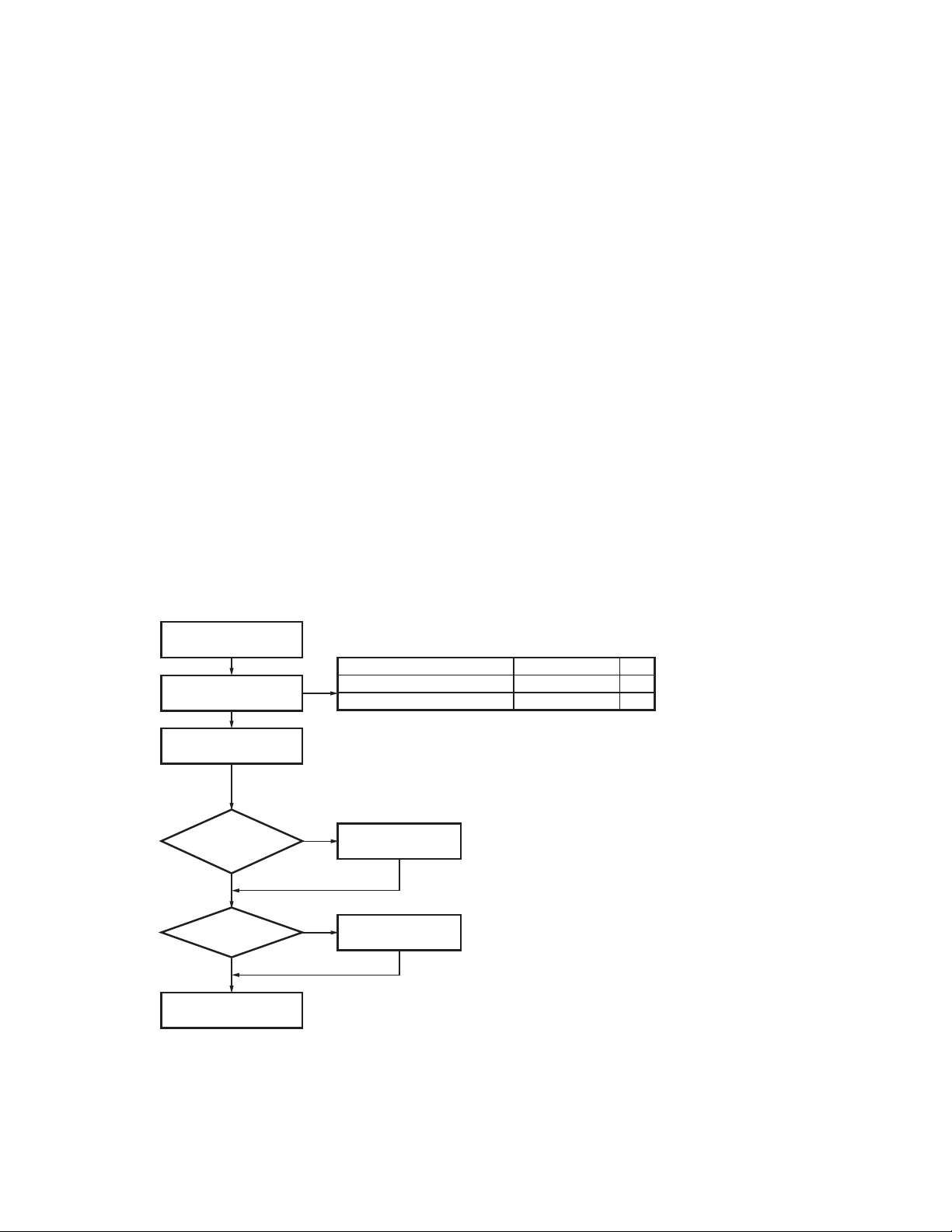
SYSTEM SET-UP
PERSONAL SAFETY
The following precautions are recommended for personal
safety :
•DONOT transmit until all RF connectors are secure and
any open connectors are properly terminated.
• SHUT OFF this equipment when near electrical blasting
caps or while in an explosive atmosphere.
• This equipment should be serviced by only qualified technicians.
SERVICE
This radio is designed for easy servicing. Refer to the
schematic diagrams, printed circuit board views, and alignment procedures contained in this manual.
Merchandise
received
Choose the type
of transceiver
Repeater
programming & setup
DC power
supply or
duplexer?
NO
External speaker?
NO
Delivery
Frequency range (MHz)
TX/RX 440~470
TX/RX 450~480
See page 4.
A personal computer (IBM PC or compatible), programming interface (KPG-46),
and programming software (KPG-91D) are required for programming.
See page 40.
The RX RF BPF (L2,L4,L5 on TX-RX unit A/2) must be aligned to obtain
the maximum sensitivity at a programmed frequency.
YES
Installation in the
optional space
YES
KES-4 or KES-5
installation
RF power
25W
25W
Type
E
K
2
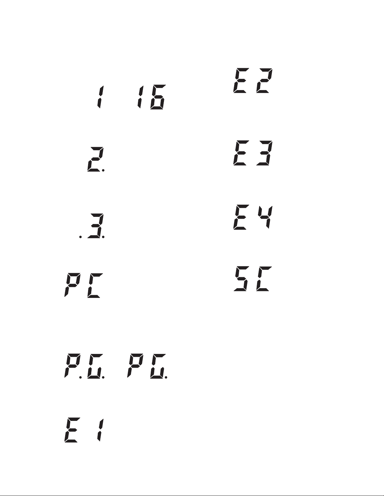
OPERATING FEATURES
TKR-851
1. Two 7-segment LED displays
• Channel display (1~16) : While operating normally in user
mode.
• When the displayed channel is contained in scan sequence, the right side decimal point is displayed.
• When the displayed channel is the priority channel, the left
side decimal point is displayed.
• “E2” is displayed when the channel data is not written.
• “E3” is displayed when PLL is unlocked.
Receiver PLL unlocked = BUSY LED blinks.
Transmitter PLL unlocked = TX LED blinks.
• “E4” is displayed when PTT is attempted on a channel
number that has no frequency data programmed.
• “PC” is displayed while in PC mode.
• “PG” is displayed while in firmware programming mode.
2 decimal points displayed = 115,200bps
1 decimal point displayed = 57,600bps
No decimal = 38,400bps
• “E1” is displayed when FPU data is not written.
• “SC” is displayed while in scan mode.
3
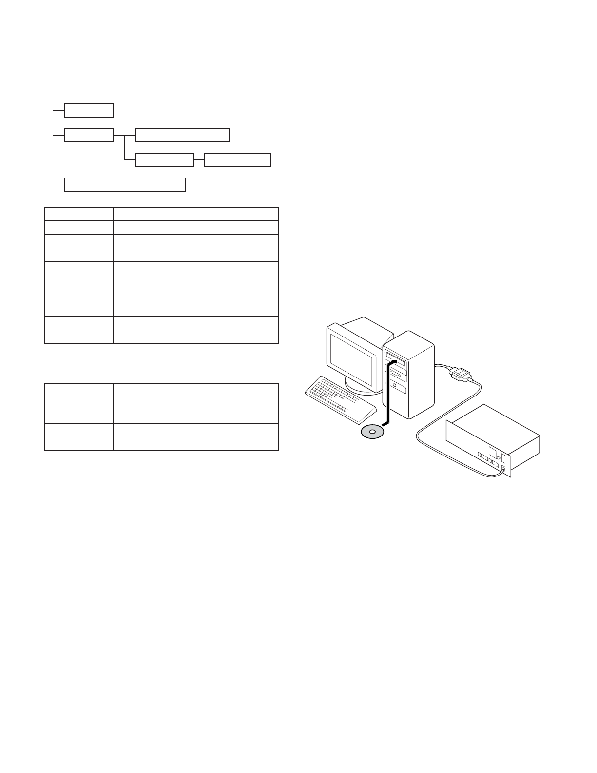
TKR-851
IBM-PC
KPG-46
KPG-91D
TKR-851
REALIGNMENT
1. Modes
User mode
PC mode
Firmware Programming mode
Mode Function
User mode Use this mode for normal operation.
PC mode Use this mode to make various settings by
PC programming Use to read and write frequency data and
mode other features to and from the repeater.
PC test mode Use to check the repeater using the PC.
Firmware pro- Use when changing the firmware program
gramming mode of the flash memory.
PC programming mode
PC test mode
means of the FPU through the RS-232C port.
This feature is included in the FPU.
PC tuning mode
3-3. KPG-46 Description (PC Programming Inter-
face Cable : Option)
The KPG-46 is required to interface the TKR-851 to the
computer. It has a circuit in its D-sub connector (25-pin) case
that converts the RS-232C logic level to the TTL level.
The KPG-46 connects the microphone connector of the
TKR-851 to the computer’s RS-232C serial port.
3-4. Programming Software Description
The KPG-91D is the programming software for TKR-851
supplied on a CD-ROM. This software runs under Windows
98, ME, Windows 2000 or XP on an IBM-PC or compatible
machine.
The data can be input to or read from TKR-851 and edited
on the screen. The programmed or edited data can be
printed out. It is also possible to tune the transceiver.
3-5. Programming With IBM PC
Data can be programmed into the flash memory in RS232C format via the microphone connector.
2. How to Enter Each Mode
Mode Operation
User mode Power on.
PC mode Received commands from PC.
Firmware Pro- [PF1] key + Power on (one second).
gramming mode
3. PC Mode
3-1. Preface
The TKR-851 repeater is programmed by using a personal
computer, programming interface and KPG-91D software.
3-2. Connection Procedure
1. Connect the TKR-851 to the personal computer with the
interface cable.
2. When power is applied, the user mode is entered immediately. When the PC sends a command, the repeater enters the PC mode and displays “PC” on the 7-segment
LED. When data is being transmitted to the PC from the
repeater, the TX LED flashes. The BUSY LED flashes
when data from the PC is being received by the repeater.
Note :
• The data stored in the personal computer must match the
model type, when it is written into the flash memory.
• Change the TKR-851 to PC mode, then attach the interface cable.
Fig. 1
4. Firmware Programming Mode
4-1. Preface
The TKR-851 uses flash memory to allow it to be easily
upgraded when new features are released in the future.
4-2. Connection Procedure
Connect the TKR-851 to the personal computer (IBM PC
or compatible) with the interface cable (KPG-46). (Connection
is the same as in the PC mode.)
Notes :
You can only program firmware from the 8-pin microphone connector on the front panel. Using the 25-pin logic
interface on the rear panel will not work.
4

REALIGNMENT / INSTALLATION
TKR-851
4-3. Programming
1. Start up the programming software (Fpro. exe).
2. Set the communications speed (normally, 115200 bps)
and communications port in the configuration item.
3. Set the firmware to be updated by file name item.
4. Turn the TKR-851 power on with the [PF1] key held down.
Hold the key down for one second until the 7-segment
display changes to “P.G.”. When “P.G.” appears, release
your finger from the key.
5. Check the connection between the TKR-851 and the personal computer, and make sure that the TKR-851 is in the
program mode.
6. Press write button in the window. A window opens on
the display to indicate progress of writing.
7. If writing ends successfully, the TX LED on the TKR-851
lights.
8. If you want to continue programming other TKR-851s, repeat steps 3 to 6.
Notes :
This mode cannot entered if the firmware program mode
is set to disable in the programming software (KPG-91D).
4-4. Function
If you press the [PF1] key (front panel), both decimal point
on the 7-segment display will disappear. The writing speed is
38400 bps (low-speed mode). If you press the [PF1] key
again, the right hand decimal points will light. The writing
speed is 57600 bps (middle-speed mode).
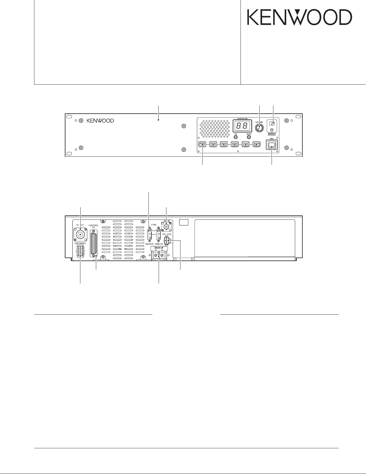
INSTALLATION
1. External Power Supply Connection
(Rear Connectors)
This unit has two external power supply connectors : Main
DC and Backup.
If an external DC power supply is connected to the main
DC connector and a backup battery is connected to the
Backup connector at the same time, the DC power supply
switches to the battery automatically if power failure occurs.
Therefore, the operation of the repeater can be continued.
If the battery is used, but both the battery and power supply need not be connected (if an external switch is used or if
only a solar battery is used), connect it to the Backup connector, not the Main DC connector. Current consumption can be
reduced by approx. 120mA because the relay is not used.
If it is installed when the temperature at the repeater site
is below freezing, check whether the switch (relay) works
properly after installation.
2. Voice Scrambler
It operates only during base operation. The voice is not
scrambled when it is repeated.
2-1. Modification
1) Remove R742 and R653 on the TX-RX unit (B/2) : control
section.
Note :
Normally, write in the high-speed mode (115200 bps).
2-2. Connection
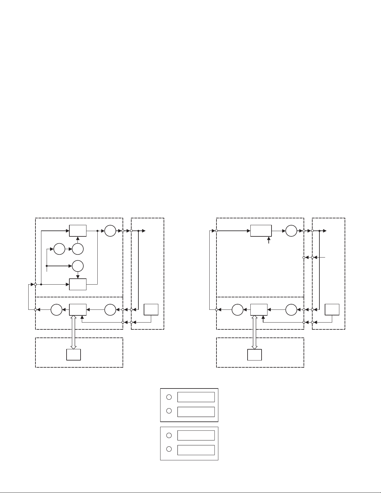
1) The functions of pins of CN601 on the TX-RX unit (B/2) :
control section are shown in the figure.
2) Join the CN601 connector to the voice scrambler board via
the E37-0808-05 connector cable.
When the operation is checked in PC test mode after the
modification, and the maximum deviation is adjusted, the
voice from the local microphone is not modulated. In this
case, remove the CN601 12-pin (PTO) cable and connect it to
the land of the display unit (X54-333) from the voice scrambler. The voice from the local microphone can be modulated
in PC test mode.
5
TKR-851
TX-RX unit (B/2)
Control section
Component side
INSTALLATION
Display unit (A/2)
Foil side
R653
CN601
PTO
SB
8C
SB
CN603
PTO
Fig. 3
3. External Speaker (KES-4 or KES-5)
1
14
CN604
CN605
R742
CN606
Fig. 1
The TKR-851 has a internal built-in speaker (5W/8Ω), and
the external speaker output from the TEST/SPKR connector
(15-pin) on the rear of the radio is 4W/4Ω. Use external
speaker KES-4 or KES-5.
3-1. Connection for the KES-4 or KES-5 With the TKR-851
■ When taking the AF output from the TEST/
SPKR connector (15-pin) on the rear of the radio
The following tools are required for changing the connec-
tor.
• Extracting tool
The following extracting tool is recommended :
Molex Inc. Order No. : J5800-002 (W05-0878-00)
TXO (MIC signal output)
TXI (MIC signal input)
RXO (RX audio signal output)
AC (Audio control signal output)
BC1 (Scramble code output 1)
BC2 (Scramble code output 2)
BC3 (Scramble code output 3)
BC4 (Scramble code output 4)
PTI (PTT signal input)
CLRC (Clear code for scrambler)
RXI (RX audio signal input)
PTO (PTT signal output)
6
CN601
1
NC
GND
14
Fig. 2
Voice
scrambler
Display
unit
8C
1. Remove the connector with jumper from the external
speaker connector on the rear panel of the radio. (Fig. 4-1)
Note : Save the jumper, which is required when the radio
is used without the external speaker.
2. Remove the terminals with the jumper from the connec-
tor housing holes number 9 and 12 using the extracting
tool.
Removing the jumper lead (Fig. 4-2)
1) Insert the extracting tool (J5800-002) into the connector while pushing the jumper lead in the direction of
(a).
2) Push the extracting tool into collapse the barbs of the
crimp terminal.
3) Pull out the lead while continuing to push the extracting
tool in the direction (b).
3. Reinsert the terminal with the black and white stripe lead
into hole number 12, and the terminal with the black lead
into hole number 6. (Fig. 4-3)
4. Attach the connector to the external speaker connector on
the radio.
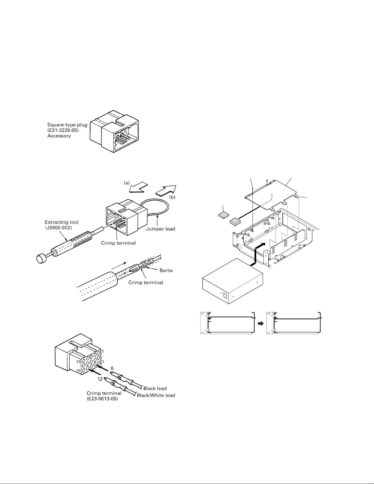
or
Hardware fixture
Insert the plate
tabs to set the
height position
(high, middle,
or low).
Tighten screws
Cushion
(G13-1801-04 or
G13-1802-04)
The top plate can be inverted to adjust the height
of the cabinet space.
INSTALLATION
TKR-851
Note :
Relationship between TEST/SPKR connector (15-pin) con-
nection and speaker output.
When pins 9 and 12 are shorted : Built-in internal speaker
is used.
When pins 9 and 12 are open and output is from pins 6 and
12 : KES-4 or KES-5 is used.
Fig. 4-1
4. Accessory Cabinet
You can install optional accessories, such as a DC power
supply or duplexers in the accessory cabinet.
1. Place the optional accessory in the cabinet as shown be-
low.
2. If necessary, attach cushions (G13-1801-04 and/or G13-
1802-04) to the top plate (J21-8402-04) in order to adjust
the space between the cabinet and the top plate. Then,
insert the 3 tabs of the plate into the slots in the side of the
cabinet. High, middle, or low positions are available. To
afix the plate, inset and tighten 2 screws on the other side
of the plate.
You can also flip the top plate upside-down to adjust a
height of the cabinet space.
Fig. 4-2
Fig. 4-3
Fig. 5
7
TKR-851
INSTALLATION / MODIFICATION
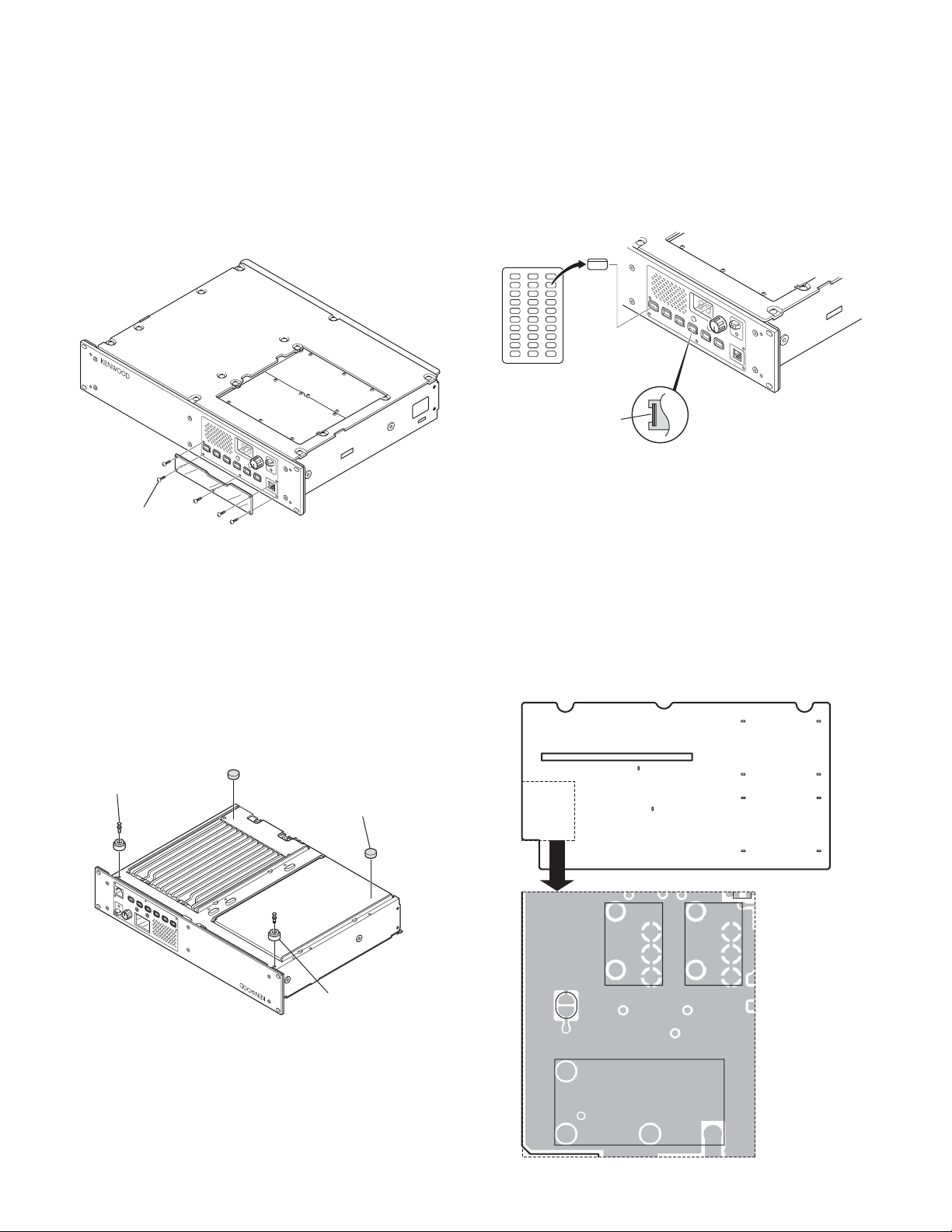
5. Key Cover
To avoid accidentally pressing the keys, you can install the
key cover.
1. Install and fix the key protector using the 5 supplied
screws (N35-3006-45).
Screws
(N35-3006-45) x 5
Fig. 6
6. Desktop Repeater
When you use the repeater on the desktop, attach the 4
spacers to the base of the repeater as shown in figure. With
these spacers attached, the front panel will not touch the
desk surface.
7. Installing Name Plates
Punch out the name plate card. Then insert the plates
onto the reltative function keys.
You can reconfigure the name plates at any time.
Punch out the
name plate cards
Squeeze and
insert the plates.
Name plates for
the function keys
Name plates
Side view of the key
Fig. 8
MODIFICATION
1. DC Source Switch
To prevent the power supply from turning off due to
misoperation of the DC source switch on the front panel or
accidents (tampering) after installation, the main unit can be
kept on regardless of the on/off of the DC source switch on
the front panel.
Short the PSW land near K1 relay by soldering.
Pegs
Firmly press these pegs
(J59-0302-05) through the
spacers to afix them to
the repeater.
Peel off the backing paper
to attach these spacers
(J02-0492-04).
Spacers
(J02-0475-05)
Fig. 7
PSW
TX-RX unit (A/2)
Component side
CF1
WIDE
K1
NARROW
CF2
8
Fig. 1
MODIFICATION
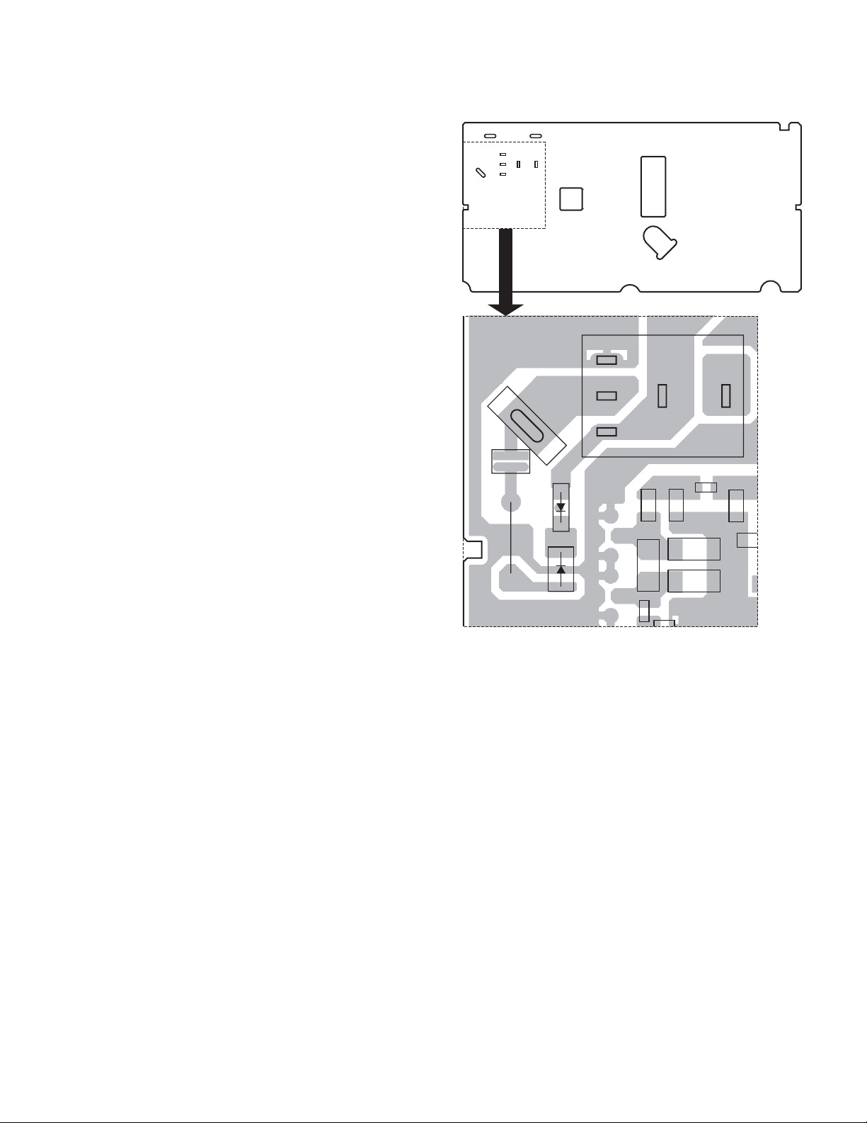
2. Trickle Charge for Backup Battery
If the external DC power supply is connected to the Main
DC connector and a backup battery (12V rechargeable type) is
connected to the Backup connector at the same time, the
battery can be trickle-charged from the external DC power
supply with a maximum current of 0.5A.
Short the CHARGE land near R61.
Notes :
1. Make this modification after removing the DC power sup-
ply and battery for safety.
2. When the DC power supply is connected after the modifi-
cation, DC voltage is output to the Backup connector. Be
careful during setup.
3. When the backup battery is used for a long time, remove
the battery from the repeater and recharge it because the
trickle charge is not sufficient for recharging a completely
discharged battery.
CN7 BACKUP
(ORANGE)
TKR-851
Final unit (A/2)
Component side
K1
CHARGE
R61
Fig. 2
9
TKR-851
w
e
e
r
t
t
q
q
t
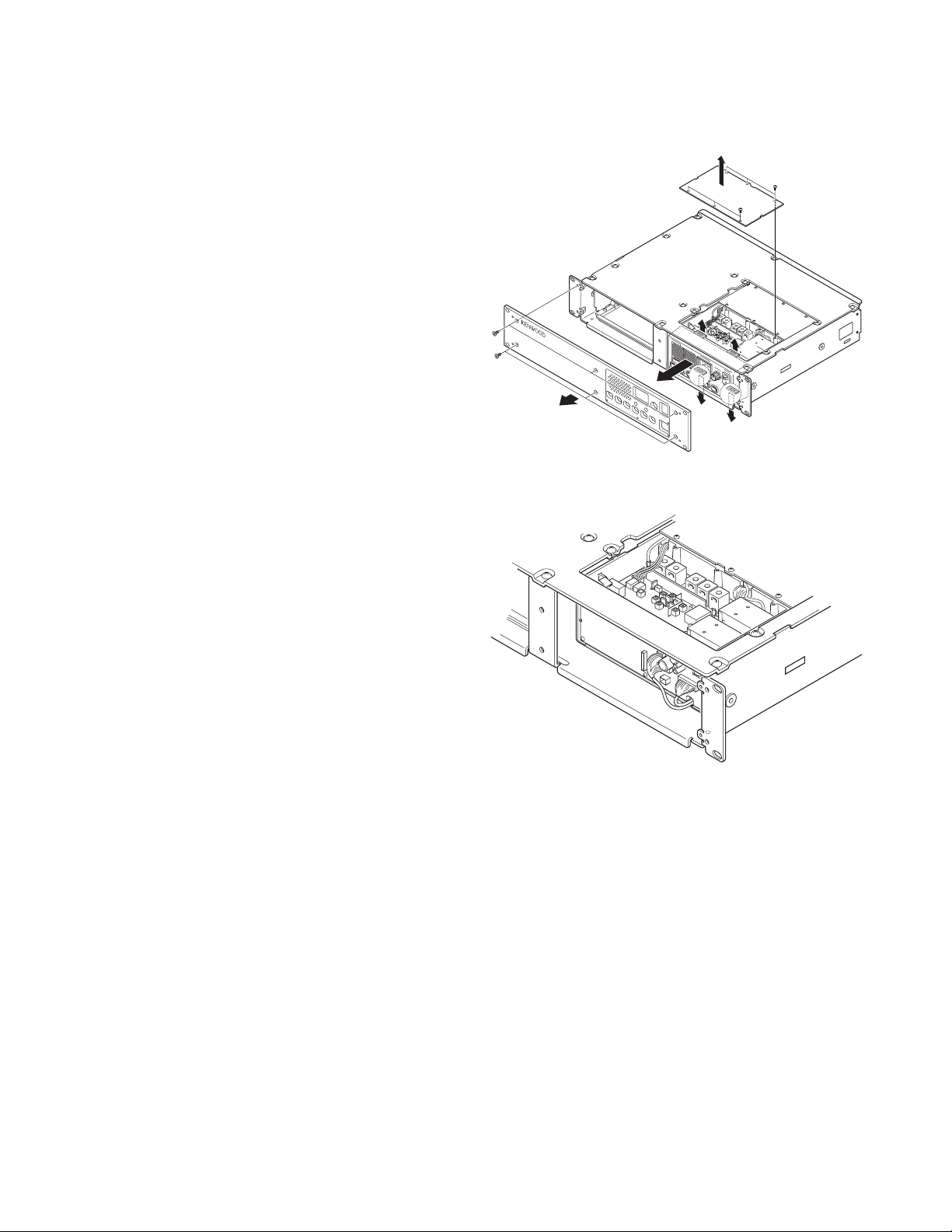
DISASSEMBLY FOR REPAIR
1. How to Remove the Panel Assy (ABS)
Note : You can remove the panel assembly (ABS) without
removing the top panel (A62-0840-03).
1. To remove panel (TX-RX, w), loose 6 screws ( q ).
2. To remove panel assembly (Front, r), loose 6 screws
( e ).
3. The panel assembly (ABS) is security fastened by 4 tabs
( t ) on top and bottom. You can remove the panel assembly by pulling to front while you are pulling up the
tabs.
10
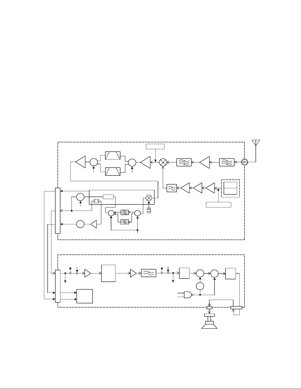
CIRCUIT DESCRIPTION
TKR-851
1. Outline
The TKR-851 is a UHF/FM repeater designed to operate in
the frequency range of 440 to 470MHz (E), 450 to 480MHz
(K).
The unit consists of receiver, transmitter, phase-locked
loop (PLL) frequency synthesizer, and control circuits.
2. Receiver Circuit
The receiver is double conversion super-heterodyne, designed to operate in the frequency range of 440 to 470MHz
(E), 450 to 480MHz (K).
The receiver circuit located in TX-RX unit (X57-696 A/2)
consists of the following : 2-1 front-end circuit, 2-2 first mixer,
2-3 IF amplifier circuit, 2-4 audio amplifier circuit, and 2-5
squelch circuit.
TX-RX unit (X57 A/2): TX-RX
MCF (Wide)
XF2
MCF (Narrow)
XF1
44.850MHz
QUD
CF1 (Wide)
D4
CF2 (Narrow)
455kHz
D1
SW
W/N
IF AMP
Q2
SWSW
D3
W/N
RSSI
Q4
DET
NOISE DET
SQL
IF AMP
Q3
SW
W/N
D5
DET
D2
SW
W/N
FM SYSTEM IC
IC9
NOISE AMP
Q7
2-1. Front-end Circuit
The front-end circuit consists of BPF L2, RF amplifier Q1,
and BPF L4/L5. The helical BPF covers frequency ranges 440
to 480MHz, with a passband of 5.0MHz.
The BPF L4/L5 attenuates the unwanted signals, and
sends only the necessary signal to the first mixer DBM A1.
2-2. First Mixer
The signal from the BPF is heterodyned with the first local
oscillator signal from the PLL frequency synthesizer circuit at
the first mixer DBM (A1) to become a 44.85MHz first intermediate frequency (IF) signal. The first IF signal is fed
through two monolithic crystal filters (XF2; Wide, XF1; Narrow) to further remove spurious signals.
44.85MHz
1st MIX
DBM A1
X1
44.395MHz
LPF
BPF
L4,L5
IF AMP
Q10
RF AMP
Q1
IF AMP
Q9
IF AMP
Q8
fRX–44.85MHz
BPF
L2
RX VCO
A3 (X58-480)
VCO A
VCO B
RX ANT
TX-RX unit (X57 B/2): Control
DEI DEO
RD
ASQ
RSSI
AMP
IC608
IC604
CPU
AINR
CODEC
IC614
AMP
IC619 (B/2)
AOUTR
LPF
IC619 (A/2)
Fig. 1 Receiver circuit
RXI RXO
SPM
RA
AM
IC615
DAC
IC621
IC622
SW
INV
Q606
Q605
INT SP
MUTE
IC629
AF
AMP
11
TKR-851
CIRCUIT DESCRIPTION
2-3. IF Amplifier
The first IF signal is amplified by Q2 and Q3, and then enters IC9 (FM system IC). The signal is heterodyned again
with a second local oscillator signal (44.395MHz) with in IC9
to become a 455kHz second IF signal. The second IF signal is
fed through a 455kHz ceramic filter, CF1 (Wide), CF2 (Narrow) to further eliminate unwanted signal, and the quadrature
detection circuit FM-detects the signal to produce a baseband signal and output it from pin 11.
2-4. Audio Amplifier
The audio amplifier circuit is located in control section of
TX-RX unit (X57-696 B/2). The recovered audio signal obtained from IC9 is amplified by IC608, input to the AINR terminal of CODEC IC (IC614), and audio processed by DSP
(IC618).
The processed audio signal from AOUTR terminal of
IC614 is amplified by IC619 (B/2) to a sufficient level, antialiasing filtered by IC619 (A/2). The audio signal goes to an
electronic volume (IC615) V3/V4, to the input of multiplexer
IC (IC622), and is amplified to drive a loudspeaker by an audio
power amplifier (IC629). The 4W audio output can be provided to external 4 ohms speaker through the 15-pin test connector “SPO, SPG” on the rear panel.
2-5. Squelch Circuit
The output signal from IC9 enters FM IC again, then
passed through a band-pass filter.
The noise component output from IC9 is amplified by Q7
and rectified by D5 to produce a DC Voltage corresponding to
the noise level. The DC voltage is sent to the analog port of
the CPU (IC604).
IC9 outputs a DC voltage (RSSI) corresponding to the input of the IF amplifier.
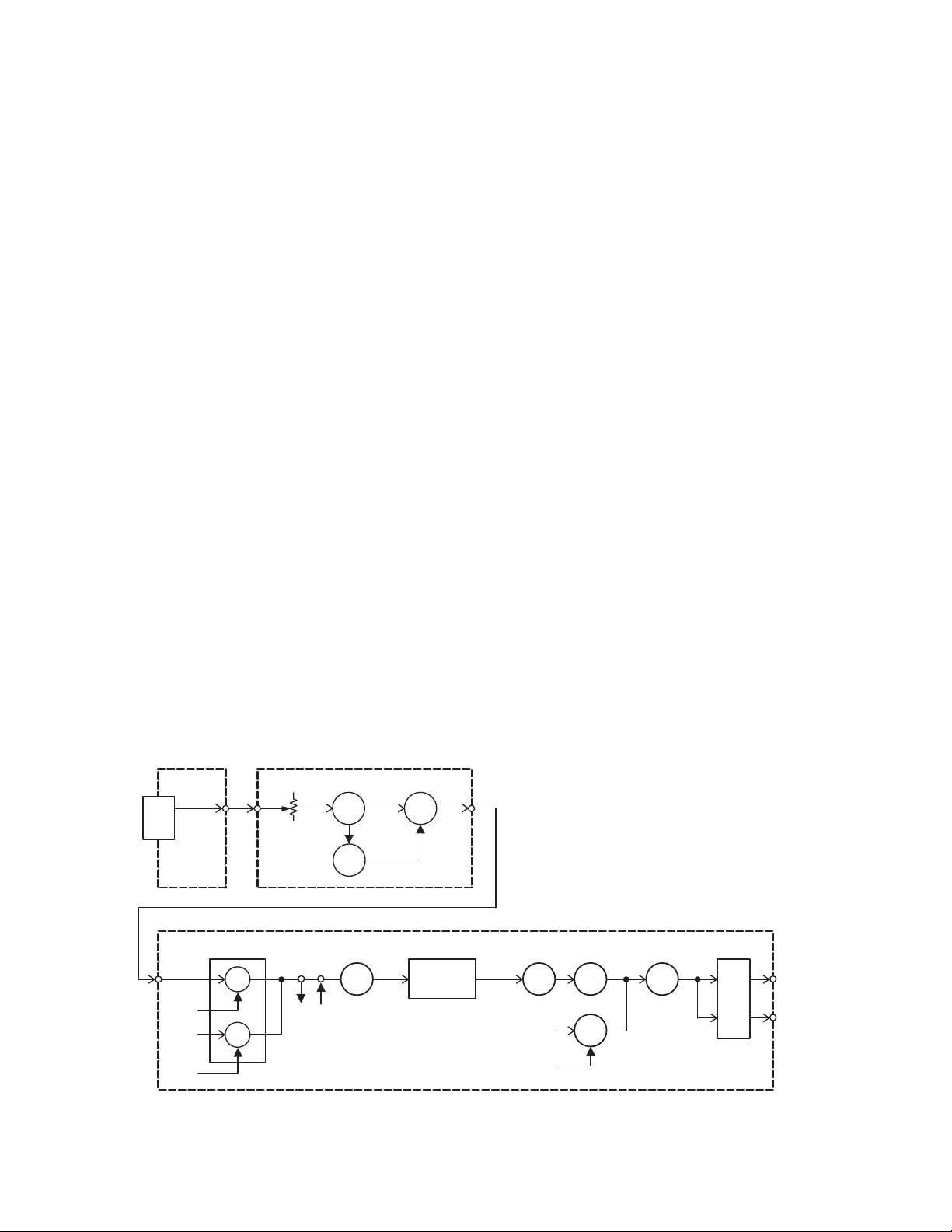
3. Transmitter Circuit
The transmitter circuit consists of the following circuits : 31 microphone circuit, 3-2 modulation level adjustment circuit,
3-3 driver and final power amplifier circuit, 3-4 automatic
power control circuit, 3-5 RF power down detect, and 3-6 fan
action control circuit.
3-1. Microphone Circuit
The signal from the microphone is passed through AGC
circuit located in display unit (X54-333), so that it does not
saturate. This circuit consists of IC501, D501, D502, Q501,
and Q502. The AGC is operated by controlling the + and –
side levels of amplitude using the current obtained by positive and negative detection of the amplified audio signal. The
audio signal goes to control section of TX-RX unit (X57-696 B/
2) from display unit (X54-333).
The transmit audio signal goes to the input of the multiplexer IC (IC605) for microphone muting. The audio signal is
amplified by IC610, input to the AINL terminal of CODEC IC
(IC614), and audio processed by DSP (IC618). The processed
audio signal from the AOUTL terminal of IC614 is amplified
by IC616 (A/2) to a sufficient level, anti-aliasing filtered by
IC616 (B/2), and amplified by the summing amplifier IC611
(A/2).
3-2. Modulation Level Adjustment Circuit
The output of the summing amplifier IC611 (A/2) is passed
to an electronic volume (IC615) for maximum deviation adjustment before being applied to a varactor diode in the voltage controlled oscillator (VCO) A2 located in TX-RX unit (X57696 A/2).
12
Display unit
(X54 B/2)
MIC JACK
J601
TXRX unit (X57 B/2): CONTROL
MIC
MIS
TA
TAS
Display unit (X54 A/2)
VR501
IC605 (A/2)
SW
TXO TXI
SW
IC501(A/2)
AMP
DET
IC610
AMP
Q501,502
D501,502
AINL
ATT
IC614
CODEC IC
Fig. 2 Microphone circuit
MIC
AOUTL
IC616
(B/2)
AMP
D-SUB
TD
TDS
IC616
(A/2)
IC605 (B/2)
SW
IC611
(A/2)
AMPLPF
IC615
MO
DAC
MB
CIRCUIT DESCRIPTION
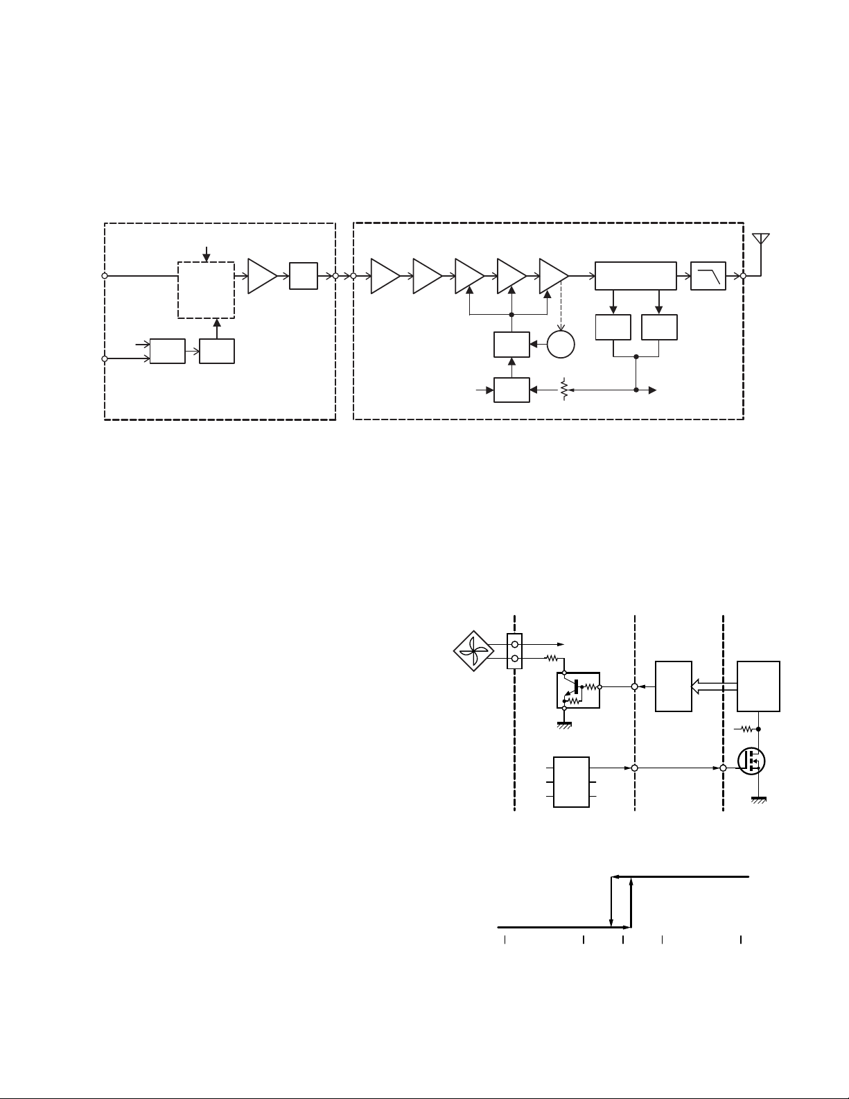
3-3. Driver and Final Power Amplifier Circuit
The transmit signal is generated by the TX VCO (A2), amplified by Q11, and sent to final unit (X45-374). This amplified
signal is amplified by Q1, Q2, Q3 and Q4, and is passed to the
FINAL stage. The RF power amplifier consists of MOS FET.
TKR-851
TX-RX unit (X57-696 A/2)
MO
FCT
MB
BUFF
IC1
STT
TX VCO
A2
(X58-481)
TCXO
X3
16.8MHz
Q11
ATT
Final unit (X45-374 A/2)
Q1
Drive
AMP
Fig. 3 Driver and final power amplifier circuit
3-4.
Automatic Power Control, Circuit and Transmitter
The automatic power control (APC) circuit stabilizes the
transmitter output power at a pre-determined level, and consists of forward/reverse power detector circuits, and switching transistor Q8. The forward/reverse power detector circuits detects forward RF power and reverse RF power to DC
voltage, and consists of a CM coupling type detection circuit
formed by a strip line, RF detector D4/D5, and DC amplifier
IC3 (A/2).
The voltage comparator (IC3 B/2) compares the above detected voltage with a reference voltage, set using the microprocessor and IC6 located in the TX-RX unit. An APC voltage
proportional to the difference between the sensed voltage
and the reference voltage appears at the output of IC3. This
output voltage controls the gate voltage for the drive amplifiers Q3 and Q4 and final amplifier Q5, which keeps the transmitter output power constant.
3-5. RF Power Down Detect
When the transmitter output power has dropped to or below the preset values (High Power : 10 W, Low Power : 0.4
W) in “RF Power Down Detect” adjustment, IC604 (CPU :
X57-696) detects the drop in power and outputs a Low-level
(default) signal to the AUX out port.
PC
IC3
Q4
Drive
AMP
DC
AMP
REF
AMP
IC3
Vcont
POWER ADJ
Q5
Final
AMP
CM COUPLER
TEMP
D4 D5
FWD
DET
Q8
SW
VR1
REV
DET
PDT
(to IC604 CPU)
Q2
Drive
AMP
Q3
Drive
AMP
This signal turns Q9 in the final unit ON to run the cooling
fan. It has a hysteresis of approx. 2°C by IC1. If fan action is
set to “Continuous”, the fan operates continuously, but Q9
stays ON.
FAN
CN4
X45 A/2 X57 A/2 X57 B/2
FAB
FAG
+B
IC1
Q9
FAS
TMP
13
IC7
Q6
CK,
DT,
STB
[Fan operation]
TX ANT
IC604
CPU
TMP
17
Q602
ON
3-6. Fan Action Control Circuit
If fan action is set to “Temperature”, the cooling fan is
turned ON or OFF according to temperature.
If the ambient temperature of the final unit exceeds
approx. 35°C, the output from the temperature detection IC1
changes from H to L. This signal is sent to the CPU (IC604)
by Q602 in the TX-RX unit B/2 (control section), and the output from pin 13 (FAS) of IC7 in the TX-RX unit A/2 controlled
by the CPU goes H.
OFF
+20°C +30°C
+35°C +40°C +50°C
Fig. 4 Fan action control circuit
13
TKR-851
VCO unit (X58-481)
VCO A
IC300
Q355
Q350
Q300
Q302
VCXO
X3
TX-RX unit
IC604
AMP
AMPLPF
PLL-IC
µ-com
CP,DP
EPT,LDT
MO
MOMO
CIRCUIT DESCRIPTION
4. PLL Frequency Synthesizer
The PLL frequency synthesizer circuit consists of the fol-
lowing circuits : 4-1 receiver PLL circuit, 4-2 transmitter PLL
circuit, and 4-3 unlocked detector circuit.
4-1. Receiver PLL
The receiver PLL circuit is located in VCO unit A3 (X58-
480) on TX-RX unit (X57-696 A/2), and consists of VCXO X2,
VCO’s (Q350 and Q351), a single-chip PLL IC IC300, buffer
amplifier Q355, and high-frequency amplifier Q302.
The VCXO generates 16.8MHz. The frequency stability is
within ± 1.5ppm (Temperature range of –30 to +60°C). The
frequency tuning of the VCXO is done to apply a voltage to
pin 1 of the VCXO. The output of the VCXO is applied to pin 8
of the PLL IC through the pin 7 of the VCO.
The first local oscillator is a lower heterodyne local oscilla-
tor, and the VCO oscillator frequency is 405.15 to 435.15MHz
(K), 395.15 to 425.15MHz (E).
The oscillator frequency is controlled by applying the VCO
control voltage, obtained from the phase comparator to the
varactor diodes.
VCO unit (X58-480)
Q354
SW
Q350
VCO A
SW
Q355
AMP
Q352
TX-RX unit
4-2. Transmitter PLL
The transmitter PLL circuit is located in VCO unit A2 (X58-
481) on TX-RX unit (X57-696 A/2), and consists of VCXO X3,
VCO’s (Q350), a single-chip PLL IC IC300, buffer amplifier
Q355, and high-frequency amplifier Q302.
The VCXO generates 16.8MHz. The frequency stability is
within ± 1.5ppm (Temperature range of –30 to +60°C). The
frequency tuning and modulation of the VCXO are done to
apply a voltage to pin 1 of the VCXO. The output of the VCXO
is applied to pin 8 of the PLL IC through the pin 7 of the VCO.
The VCO oscillator frequency is 450.00 to 480.00MHz (K),
440.00 to 470.00MHz (E).
The oscillator frequency is controlled by applying the VCO
control voltage, obtained from the phase comparator to the
varactor diodes.
4-3. Unlock Detector Circuit
If a pulse signal appears at the LD pin of IC300, an unlock
condition occurs, causing the voltage applied to the pin of the
microprocessor to go low. The names of this pin are LDT for
TX PLL and LDR for RX PLL. When the microprocessor detects this condition, the transmitter is disabled.
14
SRR
Q300
Q353
SW
VCO B
Q351
IC300
PLL-IC
CP,DP
EPR,LDR
µ-com
IC604
Fig. 5 Receiver PLL
Q302
AMPLPF
X2
VCXO
Top view
TX VCO
(X58-481)
RX VCO
(X58-480)
VCO A : 450~480 (K)
440~470 (E)
VCO A : 440~460
VCO B : 460~480
Fig. 7 VCO oscillation frequency
Fig. 6 Transmitter PLL
(MHz)
–44.850
–44.850
CIRCUIT DESCRIPTION
TKR-851
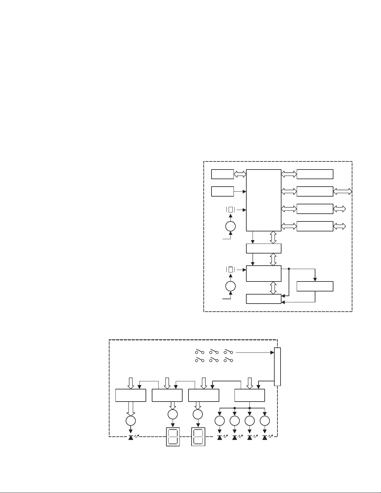
5. Control Circuit
The control circuit mainly located in the control section of
TX-RX unit (X57-696 B/2) consists of the following : 5-1 CPU,
5-2 memory circuit, 5-3 CPU clock shift, 5-4 shift register circuit, 5-5 display circuit, 5-6 DSP circuit, 5-7 base-band circuit,
5-8 RS-232C circuit, 5-9 power supply circuit, and 5-10 5-tone
decode circuit.
5-1. CPU
The CPU (IC604) is a 16bit single-chip microcomputer containing a 32k ROM and 3k RAM. This CPU controls the flash
ROM, the DSP, the receiver circuit, the transmitter circuit,
the control circuit, and the display circuit and transfers data to
or from an external device.
5-2. Memory Circuit
IC609 has a flash ROM with a capacity of 2M bits that
contains the control program for the CPU, the signal processing program for DSP and data such as channels and operating
features.
This program can be easily written from an external device. Data such as the operating status are programmed into
the EEPROM (IC600).
5-3. CPU Clock Shift
There are the 14.754MHz clock for the CPU (IC604) and
the 16.515MHz clock for the DSP (IC618) at the control section of TX-RX unit (X57-696). When these clocks are multiplexed with the reception frequency, they become an internal beat signal. To prevent this, by tuning Q600 and Q604 on
the clock frequency is shifted. (Shift on/off can be set
through programming.)
5-4. Shift Register Circuit
Serial data is sent to the shift register (IC502 to IC505 located in display unit, IC602, IC623, IC7 located in TX-RX unit)
from the CPU (IC604) to control various functions in the unit.
5-5. Display Circuit
The display circuit (X54-333) contains two 7-segment
LEDs D506, D507 (orange : see the operation manual for details of display), D503 (red : transmission), two-color D504
(green : busy, orange : selective called), two-color LED D505
(red : backup, green : main DC), LEDs in switches S501 to
S506, IC502, IC503, IC504, and IC505 to display this model
channels and states.
IC502 to IC505 are shift registers which convert serial data
from the CPU to parallel data and light LEDs.
Q507, Q510, and Q511 are switching transistors which
control two-color LED D505.
IC506, and IC507 are three-pin power supply ICs which
produce power used for the display circuit.
TX-RX unit (X57 B/2): CONTROL
IC600
EEPROM
IC601
Reset IC
14.754
MHz
Q600
BEAT
SHIFT
16.515
MHz
Q600
BEAT
SHIFT
X600
SW
IC603/606
X601
SW
IC604
CPU
INTERFACE IC
IC618
DSP
IC614
CODEC IC
IC609
FLASH ROM
IC620
232C DRIVER
IC615
D/A IC
IC602/623
Shift Register IC
IC613
DIVIDER
Display unit (X54-3330-21 A/2)
CLK,SOE,
STB1
Shift Reg. 1
BU4094BCFV
KEY LAMP
1~6
CLK,SOE,
STB1
Shift Reg. 2
BU4094BCFV
Fig. 9 Display circuit
PF1~6
CLK,SOE,
STB1
Shift Reg. 3
BU4094BCFV
SWSW
KEY1~5
CLK,SOE,
STB1
SISISI
SOSOSO
Shift Reg. 4
BU4094BCFV
SW
TX
CALL Main DC/
BUSY
Fig. 8 Control circuit
DAT
SWSWSWSW
BACKUP
15
TKR-851
CIRCUIT DESCRIPTION
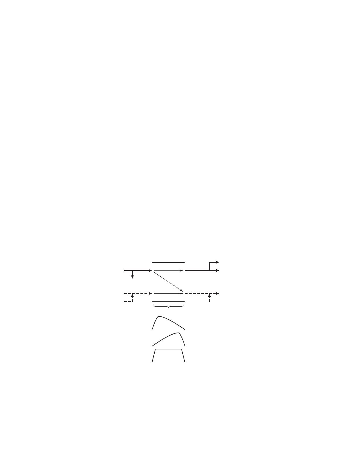
5-6. DSP
The DSP circuit filters transmit/receive audio signal and
encode/decodes signaling (QT, DQT). This circuit consists of
IC618, IC612, IC613, IC614, IC603, IC606, IC608, IC610,
IC616, and IC619.
The receive signal DET is converted from analog to digital
by IC614 with a sampling frequency of 16.128kHz. The digitized audio signal is sent to DSP IC618 to process the signaling signal and audio signal. The processed digital audio signal
is fed to CODEC IC613, converted from digital to analog, and
the analog signal is output from pin 16 (AOUTR). Then, the
audio signal is amplified by IC619 (B/2), passes through the
IC619 (A/2) low-pass filter, and goes to an electronic volume
IC615.
The transmit audio signal coming from IC605 is amplified
by IC610, fed to pin 3 (AINL) of CODEC IC614, and converted
from analog to digital at a sampling frequency of 16.128kHz.
The digitized transmit audio signal is AGC-processed, preemphasized and filtered at 300Hz to 3kHz by DSP IC618, and
the resulting signal is fed back to CODEC IC614, and converted from digital to analog, and the analog signal is output
from pin 15 (AOUTL). The transmit signal from AOUTL is
amplified by IC616 (B/2), passes through the IC616 (A/2) lowpass filter, and goes to the IC611 (A/2) summing amplifier.
IC613 is a counter IC and the clock required for the
CODEC and DSP is generated by dividing the 16.515MHz
clock signal produced by DSP IC618.
IC603 and IC606 are interface IC between the CPU operated at 5.0V and the DSP operated at 3.3V.
5-7. Base-Band Circuit
The base-band circuit switches between the modulation
signal to the transmitter circuit, and remote audio and adjusts
their levels. This circuit consists of IC605, IC607, IC611,
IC615, and IC617.
Modulation inputs include local microphone input, lowspeed data (LSD), high-speed data (HSD), external audio input (TA), and external data input (TD), and demodulation outputs include receive audio output (RA), and receive data output (RD).
The multiplexer (IC605) changes signals, the electronic
volume (IC615) adjusts the level, and the operational amplifier (IC607, IC611, IC617) amplifiers and sums signals.
5-8. RS-232C Circuit
The RS-232C circuit connects the RS-232C serial port of a
personal computer directly to this model to perform FPU operation. The FPU operation can also be performed by connecting a programming cable (KPG-46) to the local microphone on the front panel. But, if the D-sub connector on the
rear panel is used, the programming cable is not required.
The 232C driver IC (IC620) changes the TTL-232C level. The
firmware can only be rewritten with the local microphone on
the front panel.
5-9. Power Supply Circuit
The power supply circuit generates power to operate the
CPU, DSP, flash ROM, bi-directional buffer, and base-band
circuit. This circuit consists of IC624, IC625, IC626, IC627,
IC628, and IC630.
CODEC IC
RX detected signal
(AINR)
RD
TX modulation signal
Local Mic
TA
(AINL)
REPEAT
IC614 : AK4550VT
2
RX
REPEAT
3
TX
300Hz 3kHz[Frequency response]
16
(AOUTR)
15
(AOUTL)
(De-emphasis)RX
(Pre-emphaisi)TX
(300Hz~3kHz Flat)
RA
RX audio
amp.
TX VCO
(Modulation
circuit)
TD
Fig. 10 An audio signal course and the frequency characteristic
16
CIRCUIT DESCRIPTION
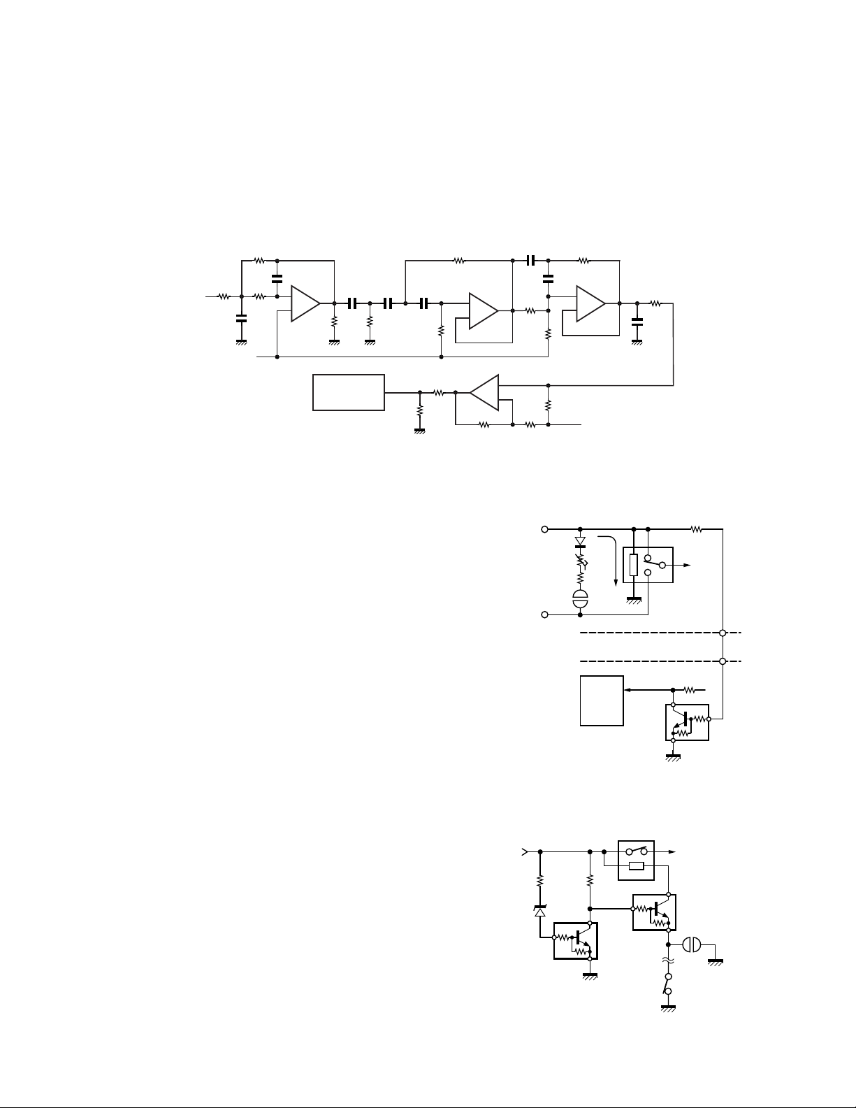
5-10. 5-tone* Decode
The 300 to 3000Hz frequency characteristics of the signal
that enters the comparator are made flat by the circuit, and
the band is made into that band required to detect 5-tone
signal by the low-pass filter (IC632 2/2), high-pass filter
(IC632 1/2) and BEF filter (IC631 1/2). The signal made into a
square wave by the comparator (IC631), and input to the
CPU, IC604.
R831
TKR-851
IC604 checks the square wave frequency for the presence of the required tone, and if the tone matches, IC604
performs the subsequent required processing.
* : The 5-tone signalling is used only the E markets.
R828
C833
R827
R833
IC611-7 pin
C840
BIAS
R832
C839
–
+
IC632
(1/2)
C838 C837 C836
R822
R830
IC604
P3
5TONE
Fig. 11 5-tone decode
6. DC Power Supply Circuit
6-1. DC Source Switching Relay Circuit
1. The final unit contains a relay (K1) for switching between
the Main DC and Backup Battery.
If an external power source is connected to the Main DC
terminal, the Backup terminal is isolated by the relay. If
the Main DC turns OFF due to power failure, it is switched
to the Backup terminal by the relay.
The CPU monitors which is used, Main DC or Backup Battery.
2. Trickle charge circuit
If both Main DC and Backup Battery are connected, trickle
charging of 0.5 A max. can be performed from the Main
DC power supply to the Battery.
(The default is OFF. See the Modification section for information on the modification method.)
The battery is charged from the Main DC with D8, D9 and
R61. If it exceeds 0.5 A, the charging circuit is turned OFF
by D9.
R829
R818
R819
D8
D9
R61
Land
C832
–
+
R821
BIAS
IC611-7 pin
IC631
(1/2)
120mA
BUP
IC604
CPU
R824
C830
R55
+B
K1
(Relay)
Final unit (A/2)
TX-RX unit (A/2)
TX-RX unit (B/2)
16
Q601
IC631
(2/2)
IC632
(2/2)
–
+
R826
R825
–
+
R820R823
Main
DC
Backup
battery
Fig. 12 DC source switching relay circuit
6-2. SB Switching Relay Circuit
1. SB (Switched +B) is supplied through the relay (K1) in the
TX-RX unit A/2.
When S507 (DC source switch) in the display unit is
turned ON, the relay (K1) is turned ON to output SB.
2. If +B exceeds 18V, the relay is forcibly turned OFF by D12
and Q25 to interrupt the power and protect the main unit.
K1
+B
R165 R166
D12
Q25
Q24
S507
SB
Land
(PSW)
Display unit
(Front panel)
Fig. 13 SB switching relay circuit
17
TKR-851
SEMICONDUCTOR DATA
Main CPU : 30622M4A-487GP (TX-RX unit IC604)
■ Pin Function
Pin No. Name I/O Function
1 IO5 I/O Aux I/O No.5 (Acc D-sub 25 pin)
2 IO4 I/O Aux I/O No.4 (Acc D-sub 25 pin)
3 5TN I 5-tone input
4 IO2 I/O Aux I/O No.2 (Acc D-sub 25 pin)
5 IO1 I/O Aux I/O No.1 (Acc D-sub 25 pin)
6 BYTE – 5V
7 CNVss – GND
8 ENT O TX PLL IC enable
9 ENR O RX PLL IC enable
10 Reset I Microcomputer reset input
11 Xout – 14.7456MHz
12 Vss – GND
13 Xin – 14.7456MHz
14 Vcc – 5V
15 NMI – Not used
16 BUP I Backup battery detect
H : Backup, L : Main
17 TEMP I Temperature detect for fan action
H : Temp high, L : Temp low
18 INTy I INT request from DSP
19 CLK O Common clock
20 DAT O Common data
21 SFT O Beat shift H : On, L : Off
22 LD1 O Control D/A converter LD
23 IO3 I/O Aux I/O No.3 (Acc D-sub 25 pin)
24 BEEP O Beep output
25 LD2 O D/A converter 2LD
26 RS O DSP reset H : Off, L : On
27 EPTT O Acc PTT (Acc D-sub 25 pin)
H : Off, L : On
28 PTT I Mic PTT H : Off, L : On
29 TXD1 O Mic TXD
30 RXD1 I Mic HOOK/RXD
31 SCLK O EEPROM clock
32 SDAT I/O EEPROM data
33 TXD0 O Acc TXD (Acc D-sub 25 pin)
34 RXD0 I Acc RXD (Acc D-sub 25 pin)
35 CP O PLL IC clock
36 DP O PLL IC data
37 RDY I CPU ready input
Pin No. Name I/O Function
38 ALE – Not used
39 HOLD – Not used
40 HLDA – Not used
41 BCLK O Not used
42 RD O Flash ROM WR/DSP HDS1
43 BHE – Not used
44 WR O Flash ROM WR/DSP HDS2
45 STB2 O Control shift register STB
46 INTx O DSP interrupt H : Off, L : On
47 HCS O DSP HCS
48 CS0 O Flash ROM CS
49 A19 O Not used
50~59 A18~A9 O Flash ROM address bus
60 Vcc – 5V
61 A8 O Flash ROM address bus
62 Vss – GND
63~70 A7~A0 O Flash ROM address bus
71 EMON I Acc monitor (Acc D-sub 25 pin)
H : Off, L : On
72 LDR I RX VCO lock detect
H : Lock, L : Unlock
73 LDT I TX VCO lock detect
H : Lock, L : Unlock
74,75
76~78
79~86 D7~D0 I/O Flash ROM data bus
87 FWD I RF power down level input
88 RSSI I RSSI level input
89 ASQ I Squelch level input
90 VLI I Volume level input
91 BATT I Power supply voltage level input
92 AI1 I Aux input No.1 (Acc D-sub 25 pin)
93 AI2 I Aux input No.2 (Acc D-sub 25 pin)
94 AVss – GND
95 AI3 I Aux input No.3 (Acc D-sub 25 pin)
96 Vref – 5V
97 AVcc – 5V
98 STB1 O Display shift register STB
99 SOE O Shift register common OE
100 IO6 I/O Aux I/O No.6 (Acc D-sub 25 pin)
KEY5,KEY4
KEY3~KEY1
O Key matrix output
I Key matrix input
18

SEMICONDUCTOR DATA
DSP : 320VC5402PGE (TX-RX unit IC618)
■ Pin Function
Pin No. Name I/O Function
1,2 NC1,NC2 – Not used (No connection)
3 Vss – GND
4 DVDD – VDD for I/O pins (+3.3V)
5A0ONot used (No connection)
6 HD0 I/O HPI data bus
7~11 A1~A5 O Not used (No connection)
12 NC3 – Not used (No connection)
13 HAS I HPI address strobe (Pull up)
14 Vss – GND
15 NC4 – Not used (No connection)
16 CVDD – VDD for core CPU (+1.8V)
17 HCS I HPI chip select
18 HR/W I HPI read/write
19 READY I Data ready (Pull up)
20 PS O Not used (No connection)
21 DS O Not used (No connection)
22 IS O Not used (No connection)
23 R/W O Not used (No connection)
24 MSTRB O Not used (No connection)
25 IOSTRB O Not used (No connection)
26 MSC O Not used (No connection)
27 XF O CODEC control
H : Power down, L : Active
28 HOLDA – Not used (No connection)
29 IAQ – Not used (No connection)
30 HOLD I Hold (Pull up)
31 BIO I Serial data syncronize input
32 MP/MC I Not used (Pull down)
33 DVDD – VDD for I/O pins (+3.3V)
34 Vss – GND
35~38
39 HCNTL0 I HPI control 0
40 Vss – GND
41 BCLKR0 I Receive clock input
42 BCLKR1 – Not used (No connection)
43 BFSR0 I Frame sync. for receiver input
44 BFSR1 I Frame sync. for receiver input
NC5~NC8
– Not used (No connection)
(SCLK : 516.09375kHz)
(LRCK : 16.128kHz)
(LRCK : 16.128kHz)
TKR-851
Pin No. Name I/O Function
45 BDR0 I Serial data receive input
46 HCNTL1 I HPI control 1
47 BDR1 – Not used (No connection)
48 BCLKX0 I Transmit clock input
(SCLK : 516.09375kHz)
49 BCLKX1 O Master clock output
(MCLK : 4.12875MHz)
50 Vss – GND
51
52 CVDD – VDD for core CPU (+1.8V)
53 BFSX0 I Frame sync. for transmitter input
54 BFSX1 I Frame sync. for transmitter input
55 HRDY – Not used (No connection)
56 DVDD – VDD for I/O pins (+3.3V)
57 Vss – GND
58 HD1 I/O HPI data bus
59 BDX0 O Serial data transmit output
60 BDX1 – Not used (No connection)
61 IACK – Not used (No connection)
62 HBIL I Byte identification (HPI)
63 NMI I Not used (Pull up)
64 INT0 I
65 INT1 I Not used (Pull up)
66 INT2 I Boot mode select (Pull up)
67 INT3 I Not used (Pull up)
68 CVDD – VDD for core CPU (+1.8V)
69 HD2 I/O HPI data bus
70 Vss – GND
71~74
75 DVDD – VDD for I/O pins (+3.3V)
76 Vss – GND
77 CLKMD1 I Clock mode select (Pull down)
78 CLKMD2 I Clock mode select (Pull up)
79 CLKMD3 I Clock mode select (Pull down)
80 NC13 – Not used (No connection)
81 HD3 I/O HPI data bus
82 TOUT0 – Not used (No connection)
83 EMU0 I/O Emulator 0 (to JTAG connector)
HINT/TOUT1
NC9~NC12
O Boot mode select (Pull up)
(LRCK : 16.128kHz)
(LRCK : 16.128kHz)
Command interrupt from host CPU
– Not used (No connection)
19
TKR-851
SEMICONDUCTOR DATA / COMPONENTS DESCRIPTION
Pin No. Name I/O Function
84
85 TDO O
86 TDI I
87 TRST I Test reset (to JTAG connector)
88 TCK I Test clock (to JTAG connector)
89 TMS I
90 NC14 – Not used (No connection)
91 CVDD – VDD for core CPU (+1.8V)
92 HPIENA I Not used (Pull up)
93 Vss – GND
94 CLKOUT O Not used (No connection)
95 HD4 I/O HPI data bus
96 X1 – 16.515MHz (System clock)
97 X2/CLKIN – 16.515MHz (System clock)
98 RS I DSP reset input
99~104 D0~D5 – Not used (No connection)
105 A6 O Not used (No connection)
106 Vss – GND
107~109 A7~A9 O Not used (No connection)
110 NC15 – Not used (No connection)
111 Vss – GND
112 DVDD – VDD for I/O pins (+3.3V)
113~119 D6~D12 – Not used (No connection)
120 HD5 I/O HPI data bus
121~123
124 HD6 I/O HPI data bus
125 CVDD – VDD for core CPU (+1.8V)
126 NC16 – Not used (No connection)
127 HDS1 I HPI data strobe 1 (Pull up)
128 Vss – GND
129 HDS2 I HPI data strobe 2 (Pull down)
130 DVDD – VDD for I/O pins (+3.3V)
131~134 A10~A13 O Not used (No connection)
135 HD7 I/O HPI data bus
136~141 A14~A19 O Not used (No connection)
142 CVDD – VDD for core CPU (+1.8V)
143,144
EMU1/OFF
D13~D15
NC17,NC18
I/O Emulator 1 (to JTAG connector)
Test data output (to JTAG connector)
Test data input (to JTAG connector)
Test mode select (to JTAG connector)
– Not used (No connection)
– Not used (No connection)
Final Unit (X45-3742-71)
Ref. No. Part name Description
IC1 IC Thermostat
IC2 IC Voltage regulator
IC3 IC DC amplifier
Q1,2 Transistor RF amplifier
Q3,4 FET TX drive amplifier
Q5 FET Final amplifier
Q8,9 Transistor DC switch
D2 Zener diode Voltage reference
D4,5 Diode RF detector
D7 Zener diode Surge protector
D8 Diode Reverse current protection
D9 Vatistor Current protector
D10 Diode Surge absorption
D51,52 Diode Reverse connection protection
Display Unit (X54-3330-21)
Ref. No. Part name Description
IC501 MOS IC MIC amplifier
IC502~505 IC Shift register
IC506,507 IC Voltage regulator
Q501,502 Transistor Level controller
Q503,504 FET DC switch
Q506 Transistor DC switch
Q507 FET DC switch
Q508~511 Transistor DC switch
Q512~514 FET DC switch
Q516~519 FET DC switch
Q521~525 FET DC switch
D501,502 Diode AF detector
D503~505 LED LED
D506,507 LED 7 segment
D508~514 Diode Surge absorption
D601,602 Diode Surge absorption
D603 Varistor Current protector
TX-RX Unit (X57-6962-70)
Ref. No. Part name Description
IC1,2 IC Buffer amplifier
IC3~5 IC Voltage regulator
20
COMPONENTS DESCRIPTION
TKR-851
Ref. No. Part name Description
IC6 IC D/A converter
IC7 IC Shift register
IC9 IC FM IF system
IC10,11 IC Voltage regulator
IC600 IC EEPROM
IC601 IC Voltage detector
IC602 IC Shift register
IC603 IC Bus transceiver
IC604 IC CPU
IC605 IC Multiplexer
IC606 IC Bus transceiver
IC607,608 IC AF amplifier
IC609 IC Flash ROM
IC610,611 IC AF amplifier
IC612 IC Inverter
IC613 IC Counter
IC614 IC CODEC
IC615 IC D/A converter
IC616,617 IC AF amplifier
IC618 IC DSP
IC619 IC AF amplifier
IC620 IC RS-232C tranceiver
IC621 IC NAND gate
IC622 IC Multiplexer
IC623 IC Shift register
IC624~628 IC Voltage regulator
IC629 IC AF power amplifier
IC630 IC Voltage regulator
IC631,632 IC AF amplifier
Q1~3 Transistor RF amplifier
Q4 Transistor Wide/Narrow switch
Q5,6 Transistor DC switch
Q7 Transistor Noise amplifier
Q8,9 Transistor RF amplifier
Q10 Transistor Current control
Q11 Transistor RF amplifier
Q12~15 Transistor Ripple filter
Q16~19 Transistor DC switch
Q23~26 Transistor DC switch
Q27 Transistor Wide 5kHz/Narrow 4kHz switch
Q600 FET DC switch
Q601 Transistor DC switch
Q602 FET DC switch
Ref. No. Part name Description
Q603 Transistor Inverter
Q604 FET DC switch
Q605 Transistor Inverter
Q606 Transistor AF mute switch
Q607~609 Transistor DC switch
Q610 FET DC switch
Q611,612 Transistor DC switch
Q613,614 Transistor Current control
Q615 Transistor DC switch
D1~4 Diode Wide/Narrow switch
D5 Diode Noise detection
D7 Diode DC switch
D8 Diode TX switch
D11 Zener diode Surge protector
D12 Diode DC switch
D13 Diode Noise detection
D600 Diode Surge protector
D606~612 Diode Surge protector
D614~616 Diode Surge protector
D618~623 Diode Surge protector
D626 Variistor Current protector
D627,628 Diode Reverse current protector
D629 Diode Surge protector
RX VCO Unit (X58-4800-10)
Ref. No. Part name Description
IC300 IC PLL
Q300,301 Transistor Active filter
Q302 Transistor Buffer amplifier
Q350,351 FET VCO OSC
Q352~354 Transistor DC switch
Q355 Transistor Buffer amplifier
D350~353 Varicap Frequency control
TX VCO Unit (X58-4810-10)
Ref. No. Part name Description
IC300 IC PLL
Q300,301 Transistor Active filter
Q302 Transistor Buffer amplifier
Q350 FET VCO OSC
Q355 Transistor Buffer amplifier
D350,352 Varicap Frequency control
D354 Varicap Modulation
21
TKR-851
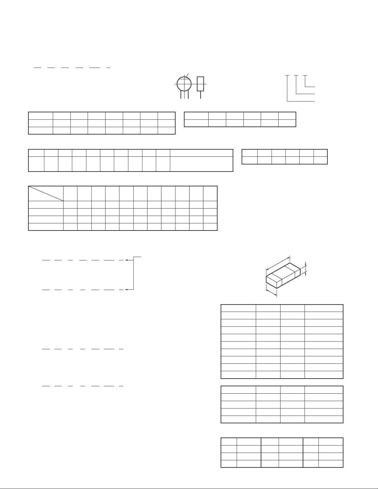
CAPACITORS
C C 4 5 T H 1 H 2 2 0 J
1234 56
1 = Type ... ceramic, electrolytic, etc. 4 = Voltage rating
2 = Shape ... round, square, etc. 5 = Value
3 = Temp. coefficient 6 = Tolerance
• Temperature coefficient
1st Word C L P R S T U
Color* Black Red Orange Yellow Green Blue Violet
ppm/°C0 –80 –150 –220 –330 –470 –750
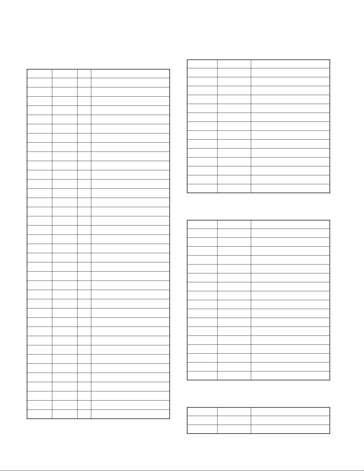
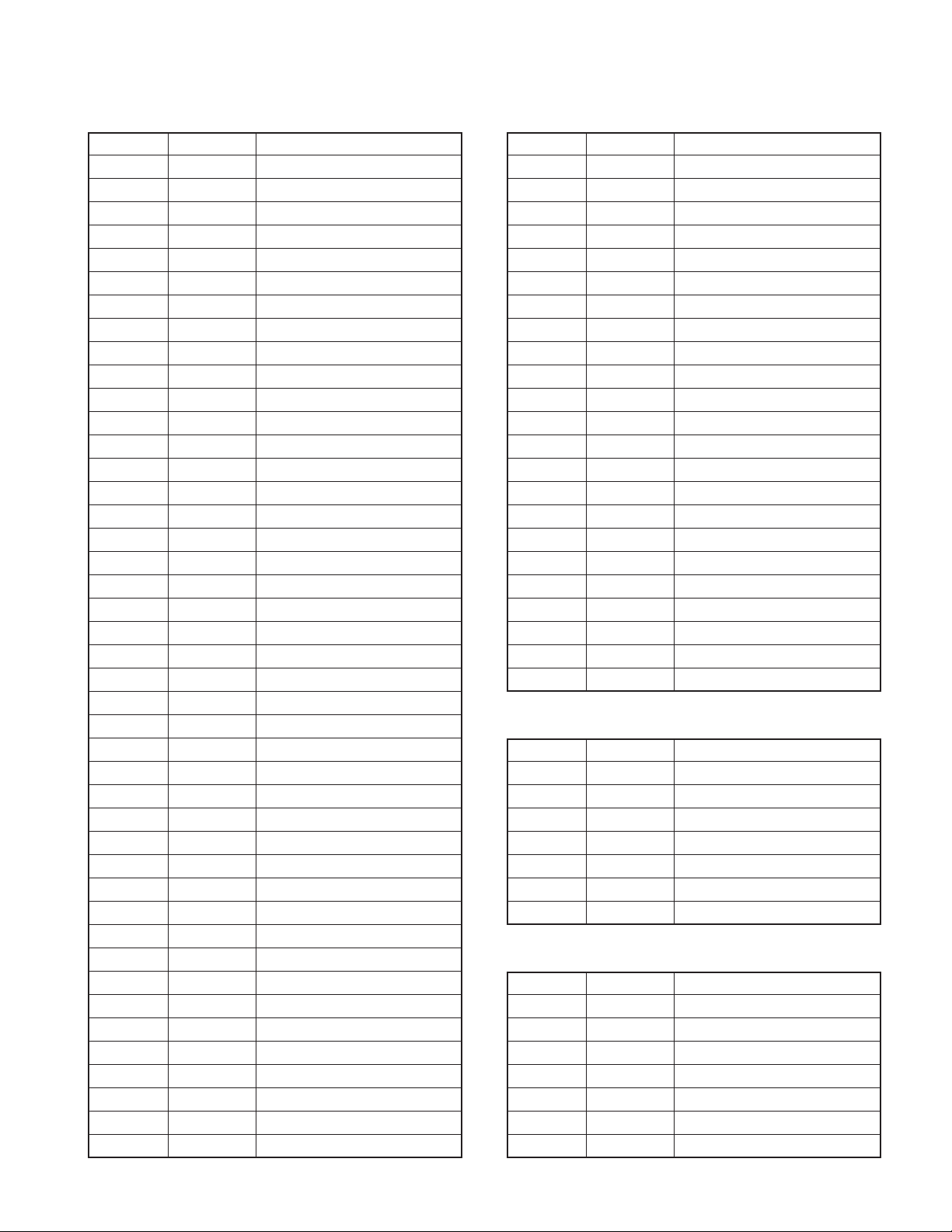
PARTS LIST
CC45
Color*
2nd Word G H J K L
ppm/°C ±30 ±60 ±120 ±250 ±500
Example : CC45TH = –470±60ppm/°C
• Capacitor value
010 = 1pF 2 2 0 = 22pF
100 = 10pF
101 = 100pF Multiplier
102 = 1000pF = 0.001µF 2nd number
103 = 0.01µF 1st number
• Tolerance (More than 10pF)
Code C D G J K M X Z P No code
(%) ±0.25 ±0.5 ±2 ±5 ±10 ±20 +40 +80 +100 More than 10µF : –10~+50
–20 –20 –0 Less than 4.7µF : –10~+75
• Voltage rating
2nd word
1st word
01.01.25 1.6 2.0 2.5 3.15 4.0 5.0 6.3 8.0 –
11012.5 16 20 25 31.540 50638035
2 100 125 160 200 250 315 400 500 630 800 –
3 1000 1250 1600 2000 2500 2150 4000 5000 6300 8000 –
ABCDEFGHJ KV
CHIP CAPACITORS
(EX) C C 7 3 F S L 1 H 0 0 0 J Refer to the table above.
12345 67 1 = Type
(Chip) (CH, RH, UJ, SL) 2 = Shape
3 = Dimension
(EX) C K 7 3 F F 1 H 0 0 0 Z 4 = Temp. coefficient
12345 67 5 = Voltage rating
(Chip) (B, F) 6 = Value
7 = Tolerance
RESISTORS
• Chip resistor (Carbon)
(EX) R D 7 3 E B 2 B 0 0 0 J
12345 67
(Chip) (B, F)
• Carbon resistor (Normal type)
(EX) R D 1 4 B B 2 C 0 0 0 J
12345 67
(Chip) (B, F)
1 = Type ... ceramic, electrolytic, etc. 5 = Voltage rating
2 = Shape ... round, square, etc. 6 = Value
3 = Dimension 7 = Tolerance
4 = Temp. coefficient
22
(Less than 10pF)
Code B C D F G
(pF) ±0.1 ±0.25 ±0.5 ±1 ±2
• Dimension
L
T
W
Chip capacitor
Code L W T
Empty 5.6±0.5 5.0±0.5 Less than 2.0
A4.5±0.5 3.2±0.4 Less than 2.0
B4.5±0.5 2.0±0.3 Less than 2.0
C4.5±0.5 1.25±0.2 Less than 1.25
D3.2±0.4 2.5±0.3 Less than 1.5
E3.2±0.2 1.6±0.2 Less than 1.25
F2.0±0.3 1.25±0.2 Less than 1.25
G1.6±0.2 0.8±0.2 Less than 1.0
H 1.0±0.05 0.5±0.05 0.5±0.05
Chip resistor
Code L W T
E3.2±0.2 1.6±0.2 1.0
F2.0±0.3 1.25±0.2 1.0
G1.6±0.2 0.8±0.2 0.5±0.1
H1.0±0.05 0.5±0.05 0.35±0.05
• Rating wattage
Code Wattage Code Wattage Code Wattage
1J 1/16W 2C 1/6W 3A 1W
2A 1/10W 2E 1/4W 3D 2W
2B 1/8W 2H 1/2W
PARTS LIST
TKR-851
✽ New Parts.
Parts without Parts No. are not supplied.
Les articles non mentionnes dans le Parts No. ne sont pas fournis.
Teile ohne Parts No. werden nicht geliefert.
Ref. No.
indicates safety critical components.
New
Address
Parts No. Description
parts
TKR-851
12BA10-4037-21 CHASSIS
21BA62-0836-04 COVER (TX/RX)
31BA62-0837-04 COVER (FINAL)
41DA62-0840-03 COVER (OUTER)
53AA62-0933-13 PANEL ASSY (INNER)
63CA62-0934-03 FRONT PANEL
81FB10-2635-04 FRONT GLASS ACCESSORY
91FB11-1259-04 FILTER ACCESSORY
10 3B ✽ B42-7158-04 STICKER (MODEL NAME)
11 1F ✽ B62-1774-00 INSTRUCTION MANUAL E
11 1F ✽ B62-1775-00 INSTRUCTION MANUAL K
12 2C,3D ✽ B72-2202-04 MODEL NAME PLATE E
12 2C,3D ✽ B72-2205-04 MODEL NAME PLATE K
14 2C E30-3414-05 DC CORD (EXT DC IN)
15 1C E30-3418-05 ANTENNA CABLE (BNC)
16 2C ✽ E30-7528-05 ANTENNA CABLE (N)
17 1E E30-3427-15 DC CORD ACCESSORY
18 1E E31-3228-05 TEST/SPKR PLUG ACCESSORY
19 1B E37-0902-05 DC WIRE (RED)
20 1B E37-0903-05 DC WIRE (BLACK)
21 2C E37-0904-05 D-SUB CABLE ASSY
22 3B E37-0905-15 SPEAKER CABLE
23 3A E37-0906-05
24 3A E37-0908-05 LEAD WIRE WITH CONNECTOR (11P)
25 2B E37-0909-05 LEAD WIRE WITH CONNECTOR (8P)
26 1B E37-0911-05 LEAD WIRE WITH CONNECTOR (3P)
27 2B E37-0912-05 COAXIAL CABLE
28 2C E37-0913-05 TEST/SPKR CONNECTOR ASSY
LEAD WIRE WITH CONNECTOR (CONT-DISP)
Desti-
nation
L : Scandinavia K : USA P : Canada
Y : PX (Far East, Hawaii) T : England E : Europe
Y : AAFES (Europe) X : Australia M :Other Areas
TKR-851 (Y54-323X-XX)
FINAL UNIT (X45-3742-71)
Ref. No.
54 1E H25-0762-04 PROTECTION BAG (120X300)
55 1F H25-2328-04 PROTECTION BAG (80/250/0.07)
57 3F ✽ H52-2013-02 ITEM CARTON CASE
59 1E J02-0475-05 FOOT ACCESSORY
60 1E J02-0492-04 FOOT ACCESSORY
61 1F J21-8402-04
64 1B J21-8467-04 HARDWARE FIXTURE (DRIVE FET)
62 1E J59-0302-05 GROMMET ACCESSORY
- J61-0307-05 BAND
65 1E K01-0418-15 HANDLE ACCESORY
66 3A K29-5389-03 KNOB (VOLUME)
67 3A K29-5460-02 KEY TOP
68 3A K29-9106-04 KNOB (DC SOURCE)
A2CN09-2292-05 HEXAGON HEAD SCREW
B 1C,2C N30-2606-46 PAN HEAD MACHINE SCREW
C 2A,1E N30-4006-46 PAN HEAD MACHINE SCREW
D 2B,2C N30-4014-46 PAN HEAD MACHINE SCREW
E1CN30-4020-45 PAN HEAD MACHINE SCREW
F 1C,2C N32-3006-46 FLAT HEAD MACHINE SCREW
G 3B,3C N32-4008-45 FLAT HEAD MACHINE SCREW
H1BN33-3006-45 OVAL HEAD MACHINE SCREW
J1EN35-3006-45
K1CN35-4006-45 BINDING HEAD MACHINE SCREW
L 1B,3B N67-3008-46 PAN HEAD SEMS SCREW W
M1C N80-2608-45 PAN HEAD TAPTITE SCREW
N2CN87-2606-46 BRAZIER HEAD TAPTITE SCREW
O3AN87-3005-45 BRAZIER HEAD TAPTITE SCREW
P 2B,3B N87-3006-46 BRAZIER HEAD TAPTITE SCREW
R2C✽ N90-3014-46 TP HEAD MACHINE SCREW
Address
New
Parts No. Description
parts
HARDWARE FIXTURE
BINDING HEAD MACHINE SCREW ACCESSORY
ACCESSORY
Destination
29 1B E37-0934-05 DC WIRE (ORANGE)
30 2C E37-0964-05 DC BACKUP WIRE (BLACK)
31 2C E37-0965-05 DC BACKUP WIRE (RED)
32 2B E37-0967-05 FLAT CABLE (36P)
33 2C E70-0402-05 DC BACKUP TERMINAL
35 1C,1E F06-1032-05 FUSE (BLADE, 10A/32V)
36 2C F09-0445-05 CAP (D-SUB) ACCESSORY
37 2C F09-0471-05 FAN MOTOR
- F10-2374-04 SHIELDING PLATE (TX/RX)
- F10-2379-04 SHIELDING CASE (TX/RX COM)
- F10-2409-04 SHIELDING CASE (TX/RX FOIL)
41 1C F20-3322-04 INSULATING SHEET (BACKUP)
43 1B,2B G02-0576-14 FLAT SPRING
44 2B G02-0829-14 FLAT SPRING
45 3B G02-0885-13 EARTH SPRING
51 1B G02-0894-04 EARTH SPRING (FINAL FET)
46 2B,3B G10-1263-04 FIBROUS SHEET (CHASSIS)
47 3C,2D G10-1264-04 FIBROUS SHEET (PANEL)
48 1F G13-1801-04 CUSHION ACCESSORY
49 1F G13-1802-04 CUSHION ACCESSORY
50 2B G13-1886-04 CUSHION (CHASSIS)
58 2C ✽ G13-2054-04 CUSHION
52 1E H25-0029-04 PROTECTION BAG (60/110/0.07)
53 1F H25-0747-04 PROTECTION BAG (250X350)
70 3A T07-0247-05 SPEAKER
- 490-0174-05 ADHESIVE TAPE
FINAL UNIT (X45-3742-71)
C1 CK73GB1H471K CHIP C 470PF K
C3 C90-2146-05 ELECTRO 100UF 25WV
C6,7 CK73GB1H471K CHIP C 470PF K
C8 CC73GCH1H080D CHIP C 8.0PF D
C10 CK73GB1H471K CHIP C 470PF K
C12-15 CK73GB1H471K CHIP C 470PF K
C17 CC73GCH1H050C CHIP C 5.0PF C
C18,19 CK73GB1H471K CHIP C 470PF K
C20 CK73FB1H471K CHIP C 470PF K
C21 CC73FCH1H120J CHIP C 12PF J
C22 CC73FCH1H060D CHIP C 6.0PF D
C23 CK73FB1H471K CHIP C 470PF K
C24 C90-4117-05 ELECTRO 100UF 16WV
C26 CC73GCH1H471J CHIP C 470PF J
C27 CK73GB1H471K CHIP C 470PF K
23

TKR-851
FINAL UNIT (X45-3742-71)
Ref. No.
C28 CK73FB1E104K CHIP C 0.10UF K
C29 CK73GB1H471K CHIP C 470PF K
C30 CK73FB1E224K CHIP C 0.22UF K
C31 C93-0599-05 CHIP C 470PF K
C32 C93-0558-05 CHIP C 8.0PF 500WV
Address
New
Parts No. Description
parts
PARTS LIST
Desti-
nation
Ref. No.
Address
CN1 E04-0154-05 PIN SOCKET
CN3 E40-5632-05 PIN ASSY
CN4 E40-3246-05 PIN ASSY
CN5 E40-5703-05 PIN ASSY
CN6-8 E23-0462-05 TERMINAL
New
Parts No. Description
parts
Destination
C33,34 C93-0565-05 CHIP C 27PF 500WV
C35 C93-0599-05 CHIP C 470PF 500WV
C36 CK73FB1E104K CHIP C 0.10UF K
C38 CK73GB1H471K CHIP C 470PF K
C39 C93-0561-05 CHIP C 12PF 500WV
C40 C93-0564-05 CHIP C 22PF 500WV
C41 C93-0599-05 CHIP C 470PF 500WV
C43 CM73F2H220J CHIP C 22PF J
C44 C93-0556-05 CHIP C 6.0PF 500WV
C46 C93-0599-05 CHIP C 470PF 500WV
C48 CK73GB1H471K CHIP C 470PF K
C49 CC73GCH1H101J CHIP C 100PF J
C50 CK73FB1E104K CHIP C 0.10UF K
C51 C90-2143-05 ELECTRO 47UF 25WV
C52 CC73GCH1H101J CHIP C 100PF J
C53 CK73FB1E104K CHIP C 0.10UF K
C54 C90-2146-05 ELECTRO 100UF 25WV
C55 C93-0599-05 CHIP C 470PF 500WV
C59 CM73F2H150D CHIP C 15PF D
C61 CM73F2H471J CHIP C 470PF J
C69 CC73GCH1H101J CHIP C 100PF J
C70 CK73FB1E104K CHIP C 0.10UF K
C71,72 CK73GB1H471K CHIP C 470PF K
C75 CK73GB1H471K CHIP C 470PF K
C77 CC73GCH1H101J CHIP C 100PF J
C78 CK73GB1H471K CHIP C 470PF K
C79 CK73FB1E104K CHIP C 0.10UF K
C80 C92-0777-05 ELECTRO 1000UF 25WV
C81 CM73F2H471J CHIP C 470PF J
C83 C93-0556-05 CHIP C 6.0PF 500WV
C86 C93-0560-05 CHIP C 10PF 500WV
C89 C93-0555-05 CHIP C 5.0PF 500WV
C91-98 CK73GB1H471K CHIP C 470PF K
C99 CK73FB1E104K CHIP C 0.10UF K
C100-102 CK73GB1H471K CHIP C 470PF K
C103 C92-0628-05 CHIP-TAN 10UF 10WV
C104 CC73GCH1H101J CHIP C 100PF J
C105 CK73GB1H471K CHIP C 470PF K
C106 CK73FB1E104K CHIP C 0.10UF K
C107 CC73GCH1H101J CHIP C 100PF J
C108 CK73FB1E104K CHIP C 0.10UF K
C109 CC73GCH1H101J CHIP C 100PF J
C112 CK73GB1H471K CHIP C 470PF K
C113 CK73FB1E104K CHIP C 0.10UF K
C114 CK73GB1H471K CHIP C 470PF K
C115 CK73FB1E104K CHIP C 0.10UF K
C116 CK73GB1H471K CHIP C 470PF K
C117 CK73FB1E104K CHIP C 0.10UF K
C118 C93-0558-05 CHIP C 8.0PF 500WV
C119 CK73GB1H471K CHIP C 470PF K
C120 CK73FB1H223K CHIP C 0.022UF K
C121,122 CM73F2H150J CHIP C 15PF J
C123,124 CM73F2H220J CHIP C 22PF J
C160 CM73F2H471J CHIP C 470PF J
C165,166 CK73FB1H471K CHIP C 470PF K
F1 F53-0190-05 FUSE
CN51,52 J13-0071-05 FUSE HOLDER
L1 L40-1075-92 SMALL FIXED INDUCTOR (10NH)
L2 L40-1075-34 SMALL FIXED INDUCTOR (10NH)
L3 L40-1875-92 SMALL FIXED INDUCTOR (18NH)
L5 L41-6865-20 SMALL FIXED INDUCTOR
L6,7 L34-4517-05 AIR-CORE COIL
L9 L34-4517-05 AIR-CORE COIL
L11 L34-4517-05 AIR-CORE COIL
L12 L34-4523-05 AIR-CORE COIL
L14 L40-1575-34 SMALL FIXED INDUCTOR (15NH)
L15 L40-1075-34 SMALL FIXED INDUCTOR (10NH)
L16 L40-1075-92 SMALL FIXED INDUCTOR (10NH)
L17 L40-1875-92 SMALL FIXED INDUCTOR (18NH)
R1 RK73GB1J103J CHIP R 10K J 1/16W
R2 RK73GB1J222J CHIP R 2.2K J 1/16W
R3 RK73GB1J470J CHIP R 47 J 1/16W
R4 RK73GB1J220J CHIP R 22 J 1/16W
R6 RK73GB1J470J CHIP R 47 J 1/16W
R7 RK73GB1J682J CHIP R 6.8K J 1/16W
R8 RK73FB2A100J CHIP R 10 J 1/10W
R9 RK73FB2A220J CHIP R 22 J 1/10W
R11 RK73GB1J104J CHIP R 100K J 1/16W
R12 RK73GB1J183J CHIP R 18K J 1/16W
R13 RK73FB2A470J CHIP R 47 J 1/10W
R14 R92-2571-05 CHIP R 270 J 1/2W
R15 R92-1259-05 CHIP R 18 J 1/2W
R16 R92-2571-05 CHIP R 270 J 1/2W
R17 RK73FB2A124J CHIP R 120K J 1/10W
R18 RK73EB2B101J CHIP R 100 J 1/8W
R19 RK73FB2A104J CHIP R 100K J 1/10W
R20,21 R92-1252-05 CHIP R 0 OHM J 1/16W
R22 R92-1213-05 CHIP R 100 J 1/2W
R23 RK73FB2A124J CHIP R 120K J 1/10W
R24 RK73FB2A104J CHIP R 100K J 1/10W
R26 RK73GB1J101J CHIP R 100 J 1/16W
R31 RK73GB1J224J CHIP R 220K J 1/16W
R34 R92-1252-05 CHIP R 0 OHM J 1/16W
R35 RK73GB1J104J CHIP R 100K J 1/16W
R36 R92-1252-05 CHIP R 0 OHM J 1/16W
R37 R92-0670-05 CHIP R 0 OHM
R38 RK73GB1J473J CHIP R 47K J 1/16W
R40 RK73FB2A101J CHIP R 100 J 1/10W
R41,42 R92-1252-05 CHIP R 0 OHM J 1/16W
R44 R92-0670-05 CHIP R 0 OHM
R45 RK73GB1J223J CHIP R 22K J 1/16W
R46 RK73GB1J471J CHIP R 470 J 1/16W
R47 RK73GB1J222J CHIP R 2.2K J 1/16W
R48 RK73GB1J471J CHIP R 470 J 1/16W
R49 R92-1217-05 CHIP R 0 OHM
R50 R92-1317-05 CHIP R 18 J 1W
R51 RK73GB1J104J CHIP R 100K J 1/16W
R52 RK73GB1J393J CHIP R 39K J 1/16W
24
TKR-851
Ref. No.
R53 RK73GB1J154J CHIP R 150K J 1/16W
R54 RK73GB1J102J CHIP R 1.0K J 1/16W
R55 RK73GB1J474J CHIP R 470K J 1/16W
R56 RK73GB1J473J CHIP R 47K J 1/16W
R57 RK73GB1J471J CHIP R 470 J 1/16W
R58 RK73GB1J474J CHIP R 470K J 1/16W
R59 R92-1252-05 CHIP R 0 OHM J 1/16W
R60 RK73GB1J103J CHIP R 10K J 1/16W
R61 R92-2687-05 RESISTOR 5.6 J 5W
R62 RK73GB1J103J CHIP R 10K J 1/16W
R72 RK73GB1J184J CHIP R 180K J 1/16W
R73 RK73FB2A101J CHIP R 100 J 1/10W
VR1 R12-6429-05 TRIMMING POT. (100K)
K1 S76-0426-05 RELAY
D2 02DZ6.2(Y) ZENER DIODE
D4,5 HSM88AS DIODE
D7 ZSA5A27 ZENER DIODE
D8 RB051L-40 DIODE
D9 MINISMDC050-02 VARISTOR
D10 1SS355 DIODE
D51,52 DSA3A1 DIODE
IC1 TK11050M ANALOG IC
IC2 NJM78L05UA BI-POLAR IC
IC3 TA75W01FU MOS IC
Q1 2SC5110(O) TRANSISTOR
Q2 2SC3356(R24) TRANSISTOR
Q3 2SK2596 FET
Q4 PD55008S DRIVE FET
Q5 RD60HUF1-01 FINAL FET
Q8 2SC4116(Y) TRANSISTOR
Q9 DTD123EK DIGITAL TRANSISTOR
TH1 PTH9M04BE471TS THERMISTOR
Address
New
Parts No. Description
parts
PARTS LIST
Destination
Ref. No.
C603 CC73GCH1H101J CHIP C 100PF J
C606 CC73GCH1H101J CHIP C 100PF J
C607 CK73GB1C104K CHIP C 0.10UF K
CN501 E40-6140-05 PIN ASSY
CN502 E40-6102-05 PIN ASSY
CN601 E40-6141-05 PIN ASSY
J601 E08-0877-05 MODULAR JACK
- J31-0543-05 COLLAR (LH-5-1.5)
CP501-504 RK75GB1J471J CHIP-COM 470 J 1/16W
R502,503 R92-1252-05 CHIP R 0 OHM J 1/16W
R505 RK73GB1J683J CHIP R 68K J 1/16W
R506 RK73GB1J103J CHIP R 10K J 1/16W
R507 RK73GB1J682J CHIP R 6.8K J 1/16W
R508 RK73GB1J102J CHIP R 1.0K J 1/16W
R509 RK73GB1J103J CHIP R 10K J 1/16W
R510 RK73GB1J224J CHIP R 220K J 1/16W
R511,512 RK73GB1J103J CHIP R 10K J 1/16W
R513 RK73GB1J104J CHIP R 100K J 1/16W
R514 RK73GB1J154J CHIP R 150K J 1/16W
R516 R92-2565-05 CHIP R 1.2K J 1/2W
R517 R92-2023-05 CHIP R 820 J 1/2W
R518,519 R92-2565-05 CHIP R 1.2K J 1/2W
R520-526 R92-2023-05 CHIP R 820 J 1/2W
R529-540 RK73GB1J102J CHIP R 1.0K J 1/16W
R541-544 RK73GB1J103J CHIP R 10K J 1/16W
R601 RK73GB1J681J CHIP R 680 J 1/16W
R604,605 RK73GB1J102J CHIP R 1.0K J 1/16W
R606 RK73GB1J473J CHIP R 47K J 1/16W
VR501 R32-0643-05 SEMI FIXED VARIABLE RESISTOR
VR601 R31-0630-05 VARIABLE RESISTOR
S501-506 S70-0410-15 TACT SWITCH
S507 S68-0410-05 PUSH SWITCH
Address
New
Parts No. Description
parts
FINAL UNIT (X45-3742-71)
DISPLAY UNIT (X54-3330-21)
TX-RX UNIT (X57-6962-70)
Destination
DISPLAY UNIT (X54-3330-21)
D503-505 B30-2151-05 LED (RED/GREEN)
C501 C92-0628-05 CHIP-TAN 10UF 10WV
C502,503 C92-0501-05 CHIP-TAN 1.5UF 10WV
C504,505 CK73GB1C104K CHIP C 0.10UF K
C506 CC73GCH1H470J CHIP C 47PF J
C507,508 CK73GB1C104K CHIP C 0.10UF K
C509 CK73GB1H103K CHIP C 0.010UF K
C510 C92-0628-05 CHIP-TAN 10UF 10WV
C511,512 CK73GB1E103K CHIP C 0.010UF K
C513-518 CC73GCH1H101J CHIP C 100PF J
C519,520 CK73GB1E103K CHIP C 0.010UF K
C521 C92-0628-05 CHIP-TAN 10UF 10WV
C522 CK73GB1C104K CHIP C 0.10UF K
C523 ✽ CK73FB1E334K CHIP C 0.33UF K
C524 C92-0628-05 CHIP-TAN 10UF 10WV
C525 CK73GB1C104K CHIP C 0.10UF K
C526 ✽ CK73FB1E334K CHIP C 0.33UF K
C601 CC73GCH1H101J CHIP C 100PF J
C602 CK73GB1H102K CHIP C 1000PF K
D501,502 HSM88AS DIODE
D506,507 LA-501DD LED
D508-514 DA204U DIODE
D601,602 DA204U DIODE
D603 MINISMDC020 VARISTOR
IC501 NJM4558E MOS IC
IC502-505 BU4094BCFV MOS IC
IC506,507 TA78L05F MOS IC
Q501 2SC4116(Y) TRANSISTOR
Q502 2SA1586(Y,GR) TRANSISTOR
Q503,504 UPA672T FET
Q506 DTA114EUA DIGITAL TRANSISTOR
Q507 UPA672T FET
Q508-511 DTA114EUA DIGITAL TRANSISTOR
Q512-514 UPA672T FET
Q516-519 UPA672T FET
Q521-524 UPA672T FET
Q525 2SK1824 FET
TX-RX UNIT (X57-6962-70)
C3 CC73GCH1H120J CHIP C 12PF J
C4,5 CK73GB1H471K CHIP C 470PF K
25

TKR-851
TX-RX UNIT (X57-6962-70)
Ref. No.
C7 CC73GCH1H120J CHIP C 12PF J
C8 CC73GCH1H0R5C CHIP C 0.5PF C
C13 CK73GB1H471K CHIP C 470PF K
C14,15 CC73GCH1H060D CHIP C 6.0PF D
C24 C92-0695-05 CHIP-TAN 10UF 10WV
Address
New
Parts No. Description
parts
PARTS LIST
Desti-
nation
Ref. No.
Address
C107 CC73GCH1H060D CHIP C 6.0PF D
C109 CC73GCH1H120J CHIP C 12PF J
C111 CC73GCH1H060D CHIP C 6.0PF D
C114-117 CC73GCH1H100D CHIP C 10PF D
C120,121 CK73GB1H471K CHIP C 470PF K
New
Parts No. Description
parts
Destination
C25 C92-0628-05 CHIP-TAN 10UF 10WV
C28,29 CC73GCH1H020C CHIP C 2.0PF C
C30 CC73GCH1H680J CHIP C 68PF J
C31 CC73GCH1H331J CHIP C 330PF J
C32 CK73GB1H103K CHIP C 0.010UF K
C33 CC73GCH1H330J CHIP C 33PF J
C34 CK73GB1H103K CHIP C 0.010UF K
C36,37 CK73GB1H103K CHIP C 0.010UF K
C38,39 CC73GCH1H680J CHIP C 68PF J
C40,41 CK73GB1H103K CHIP C 0.010UF K
C42,43 CC73GCH1H030C CHIP C 3.0PF C
C44,45 CC73GCH1H040C CHIP C 4.0PF C
C46,47 CC73GCH1H030C CHIP C 3.0PF C
C48 CK73GB1H103K CHIP C 0.010UF K
C49,50 CC73GCH1H680J CHIP C 68PF J
C51 CK73GB1H103K CHIP C 0.010UF K
C52 CK73GB1H103J CHIP C 0.010UF J
C53 CK73GB1H102K CHIP C 1000PF K
C54 CK73GB1H103J CHIP C 0.010UF J
C55,56 CK73GB1H103K CHIP C 0.010UF K
C57 CK73GB1H103J CHIP C 0.010UF J
C58 CC73GCH1H180J CHIP C 18PF J
C59 CC73GCH1H150J CHIP C 15PF J
C60 CK73GB1H103K CHIP C 0.010UF K
C61 CC73GCH1H080D CHIP C 8.0PF D
C62,63 CK73GB1H103K CHIP C 0.010UF K
C64 CK73GB1C104K CHIP C 0.10UF K
C65 C92-0628-05 CHIP-TAN 10UF 10WV
C66,67 CC73GCH1H331J CHIP C 330PF J
C68-70 CK73GB1C104K CHIP C 0.10UF K
C122,123 CK73GB1H103K CHIP C 0.010UF K
C124,125 C92-1341-05 ELECTRO 100UF 16WV
C126,127 C92-0633-05 CHIP-TAN 22UF 10WV
C128,129 CK73GB1H103K CHIP C 0.010UF K
C130,131 CK73GB1H102K CHIP C 1000PF K
C132,133 CK73GB1H471K CHIP C 470PF K
C134,135 CK73GB1H103K CHIP C 0.010UF K
C136-139 C90-4016-05 ELECTRO 47UF 16WV
C140,141 CK73GB1H103K CHIP C 0.010UF K
C142,143 CK73GB1H102K CHIP C 1000PF K
C144 CK73GB1H471K CHIP C 470PF K
C145 C92-0606-05 CHIP-TAN 4.7UF 10WV
C146 CK73GB1H471K CHIP C 470PF K
C147 C92-0633-05 CHIP-TAN 22UF 10WV
C148 CK73GB1H102K CHIP C 1000PF K
C149 CK73GB1H103K CHIP C 0.010UF K
C150 C92-0633-05 CHIP-TAN 22UF 10WV
C151 C92-0008-05 CHIP-TAN 3.3UF 16WV
C152 CK73GB1H103K CHIP C 0.010UF K
C153 CK73GB1H471K CHIP C 470PF K
C154 C92-0560-05 CHIP-TAN 10UF 6.3WV
C155 CK73GB1H103K CHIP C 0.010UF K
C156 CK73GB1H102K CHIP C 1000PF K
C157 CK73GB1H103K CHIP C 0.010UF K
C158 C92-0008-05 CHIP-TAN 3.3UF 16WV
C159 CK73GB1H471K CHIP C 470PF K
C160 CK73GB1H102K CHIP C 1000PF K
C161-163 CK73GB1H103K CHIP C 0.010UF K
C164 CK73GB1H471K CHIP C 470PF K
C166,167 CK73GB1H471K CHIP C 470PF K
C71 CK73GB1H103K CHIP C 0.010UF K
C72 C92-0628-05 CHIP-TAN 10UF 10WV
C73 CK73GB1C104K CHIP C 0.10UF K
C74 CK73GB1H102K CHIP C 1000PF K
C75 CK73GB1C104K CHIP C 0.10UF K
C76 C92-0696-05 CHIP-TAN 47UF 10WV
C77 CK73GB1H102K CHIP C 1000PF K
C78 CK73GB1C104K CHIP C 0.10UF K
C79 CK73FB1C224K CHIP C 0.22UF K
C80,81 C92-0628-05 CHIP-TAN 10UF 10WV
C82-84 CK73GB1H103K CHIP C 0.010UF K
C86 CK73GB1H102K CHIP C 1000PF K
C87 C92-0628-05 CHIP-TAN 10UF 10WV
C88 CK73GB1H102K CHIP C 1000PF K
C89,90 CK73GB1H103J CHIP C 0.010UF J
C91 CC73GCH1H040C CHIP C 4.0PF C
C92,93 CK73GB1H471K CHIP C 470PF K
C94 CC73GCH1H030C CHIP C 3.0PF C
C95 CC73GCH1H040C CHIP C 4.0PF C
C96-99 CK73GB1H471K CHIP C 470PF K
C100,101 CC73GCH1H050C CHIP C 5.0PF C
C102 CK73GB1H471K CHIP C 470PF K
C104 CK73GB1H471K CHIP C 470PF K
C105 CC73GCH1H070D CHIP C 7.0PF D
C106 CK73GB1H471K CHIP C 470PF K
26
C171 CK73GB1H471K CHIP C 470PF K
C172 CK73GB1H102K CHIP C 1000PF K
C173 CK73GB1H103K CHIP C 0.010UF K
C174 C92-0008-05 CHIP-TAN 3.3UF 16WV
C175 CK73GB1H102K CHIP C 1000PF K
C176 CK73GB1H103K CHIP C 0.010UF K
C177 CK73GB1H471K CHIP C 470PF K
C178 C92-0606-05 CHIP-TAN 4.7UF 10WV
C179 CK73GB1H103K CHIP C 0.010UF K
C184,185 CK73GB1H102K CHIP C 1000PF K
C189,190 CK73GB1H102K CHIP C 1000PF K
C191-195 CK73GB1H103K CHIP C 0.010UF K
C197 CK73FB1H333K CHIP C 0.033UF K
C198 CK73GB1C104K CHIP C 0.10UF K
C199 CK73GB1H103K CHIP C 0.010UF K
C204-208 CC73GCH1H101J CHIP C 100PF J
C210 CC73GCH1H080D CHIP C 8.0PF D
C211 CC73GCH1H120J CHIP C 12PF J
C212-214 CK73GB1H103K CHIP C 0.010UF K
C216 CK73GB1H471K CHIP C 470PF K
C217 CK73GB1H102K CHIP C 1000PF K
C218 CK73GB1E103K CHIP C 0.010UF K
C223 CC73GCH1H101J CHIP C 100PF J
C231 C92-0633-05 CHIP-TAN 22UF 10WV
C232-234 CK73GB1H103J CHIP C 0.010UF J

Ref. No.
C600 CK73GB1C104K CHIP C 0.10UF K
C602 CK73GB1C104K CHIP C 0.10UF K
C605 CK73GB1C104K CHIP C 0.10UF K
C613,614 CK73GB1E103K CHIP C 0.010UF K
C616 CK73GB1E103K CHIP C 0.010UF K
Address
New
Parts No. Description
parts
PARTS LIST
Destination
Ref. No.
C738 CK73GB1E103K CHIP C 0.010UF K
C739 CC73GCH1H181J CHIP C 180PF J
C740 CC73GCH1H101J CHIP C 100PF J
C741 CK73GB1E103K CHIP C 0.010UF K
C742 CK73GB1H471K CHIP C 470PF K
Address
New
Parts No. Description
parts
TKR-851
TX-RX UNIT (X57-6962-70)
Destination
C623 CK73GB1C104K CHIP C 0.10UF K
C629 CC73GCH1H101J CHIP C 100PF J
C634,635 CC73GCH1H220J CHIP C 22PF J
C638 CK73GB1C104K CHIP C 0.10UF K
C639 CK73GB1E103K CHIP C 0.010UF K
C640 C92-0628-05 CHIP-TAN 10UF 10WV
C641 CK73GB1C104K CHIP C 0.10UF K
C642 CK73GB1E103K CHIP C 0.010UF K
C643 C92-0628-05 CHIP-TAN 10UF 10WV
C644 CK73GB1E103K CHIP C 0.010UF K
C645,646 C92-0628-05 CHIP-TAN 10UF 10WV
C647 CC73GCH1H101J CHIP C 100PF J
C648 CK73GB1E103K CHIP C 0.010UF K
C649 CC73GCH1H330J CHIP C 33PF J
C652 CC73GCH1H101J CHIP C 100PF J
C657 CK73GB1E103K CHIP C 0.010UF K
C662 C92-0628-05 CHIP-TAN 10UF 10WV
C663 C92-0519-05 CHIP-TAN 1.0UF 25WV
C670 C92-0003-05 CHIP-TAN 0.47UF 25WV
C679 C92-0628-05 CHIP-TAN 10UF 10WV
C681 C92-0546-05 CHIP-TAN 68UF 6.3WV
C684 CC73GCH1H101J CHIP C 100PF J
C685 CK73GB1E103K CHIP C 0.010UF K
C690 CC73GCH1H101J CHIP C 100PF J
C691,692 CK73GB1E103K CHIP C 0.010UF K
C693,694 C92-0628-05 CHIP-TAN 10UF 10WV
C695,696 CK73GB1H471K CHIP C 470PF K
C697,698 C92-0628-05 CHIP-TAN 10UF 10WV
C700,701 C92-0628-05 CHIP-TAN 10UF 10WV
C703,704 CK73GB1C104K CHIP C 0.10UF K
C743 CK73GB1E103K CHIP C 0.010UF K
C744-746 C92-0628-05 CHIP-TAN 10UF 10WV
C747,748 CK73GB1E103K CHIP C 0.010UF K
C749 CK73GB1H471K CHIP C 470PF K
C750,751 CK73GB1E103K CHIP C 0.010UF K
C752 CK73GB1H471K CHIP C 470PF K
C753,754 C92-0628-05 CHIP-TAN 10UF 10WV
C755 CK73GB1H471K CHIP C 470PF K
C756,757 C92-0628-05 CHIP-TAN 10UF 10WV
C758 CK73FB1C105K CHIP C 1.0UF K
C759 CK73GB1H471K CHIP C 470PF K
C760 CK73GB1H102K CHIP C 1000PF K
C761 CK73GB1C104K CHIP C 0.10UF K
C762,763 CK73GB1H102K CHIP C 1000PF K
C764,765 CK73GB1E103K CHIP C 0.010UF K
C766-768 CC73GCH1H101J CHIP C 100PF J
C769-771 C92-0560-05 CHIP-TAN 10UF 6.3WV
C772 ✽ C92-0823-05 CHIP-TAN 100UF 10WV
C773 C92-0514-05 CHIP-TAN 2.2UF 10WV
C774 CK73FB1C105K CHIP C 1.0UF K
C775-779 C92-0519-05 CHIP-TAN 1.0UF 25WV
C780-782 CK73FB1C105K CHIP C 1.0UF K
C783 CK73GB1H471K CHIP C 470PF K
C784 CK73FB1C105K CHIP C 1.0UF K
C785,786 CK73GB1C104K CHIP C 0.10UF K
C787 CK73FB1C105K CHIP C 1.0UF K
C788 CC73GCH1H101J CHIP C 100PF J
C789 CE04EW1E331M ELECTRO 330UF 25WV
C790 CC73GCH1H101J CHIP C 100PF J
C791 CK73GB1H471K CHIP C 470PF K
C705 CK73GB1E103K CHIP C 0.010UF K
C706 C92-0628-05 CHIP-TAN 10UF 10WV
C707-709 CK73GB1E103K CHIP C 0.010UF K
C710 C92-0628-05 CHIP-TAN 10UF 10WV
C711 CK73GB1H471K CHIP C 470PF K
C712 CK73GB1E103K CHIP C 0.010UF K
C713,714 C92-0628-05 CHIP-TAN 10UF 10WV
C715 CK73GB1E103K CHIP C 0.010UF K
C716,717 CK73GB1H471K CHIP C 470PF K
C718,719 CK73GB1E103K CHIP C 0.010UF K
C720 C92-0532-05 CHIP-TAN 1.0UF 10WV
C721,722 C92-0628-05 CHIP-TAN 10UF 10WV
C723 CK73FB1C105K CHIP C 1.0UF K
C724 CK73GB1H182K CHIP C 1800PF K
C725 CC73GCH1H470J CHIP C 47PF J
C726 CC73GCH1H181J CHIP C 180PF J
C727,728 CK73GB1E103K CHIP C 0.010UF K
C729 C92-0628-05 CHIP-TAN 10UF 10WV
C730,731 CK73GB1E103K CHIP C 0.010UF K
C732 CK73GB1H471K CHIP C 470PF K
C733 C92-0628-05 CHIP-TAN 10UF 10WV
C734 CC73GCH1H270J CHIP C 27PF J
C735 CC73GCH1H150J CHIP C 15PF J
C736 CK73GB1H182K CHIP C 1800PF K
C737 CC73GCH1H270J CHIP C 27PF J
C792-794 CK73GB1H102K CHIP C 1000PF K
C795 CC73GCH1H101J CHIP C 100PF J
C796,797 CK73GB1H102K CHIP C 1000PF K
C798 CE04EW1E470M ELECTRO 47UF 25WV
C799 CK73GB1H102K CHIP C 1000PF K
C800 CE04EW1E470M ELECTRO 47UF 25WV
C801 C92-0560-05 CHIP-TAN 10UF 6.3WV
C802-805 CK73GB1H102K CHIP C 1000PF K
C806 CE04EW1E470M ELECTRO 47UF 25WV
C807-810 CK73GB1H102K CHIP C 1000PF K
C811 CE04EW1E470M ELECTRO 47UF 25WV
C812,813 CK73GB1H102K CHIP C 1000PF K
C814 C92-0777-05 ELECTRO 1000UF 25WV
C815 CK73FB1E104K CHIP C 0.10UF K
C816 CK73GB1H102K CHIP C 1000PF K
C817 CE04EW1E470M ELECTRO 47UF 25WV
C818-820 CK73GB1H102K CHIP C 1000PF K
C821,822 CC73GCH1H101J CHIP C 100PF J
C823 C92-0619-05 CHIP-TAN 47UF 4WV
C824 CK73GB1H472K CHIP C 4700PF K
C825 CK73GB1C104K CHIP C 0.10UF K
C826 C92-0560-05 CHIP-TAN 10UF 6.3WV
C827 ✽ C92-0823-05 CHIP-TAN 100UF 10WV
C828 C92-0514-05 CHIP-TAN 2.2UF 10WV
C829 CK73GB1C104K CHIP C 0.10UF K
27

TKR-851
TX-RX UNIT (X57-6962-70)
Ref. No.
C830 CK73GB1E103K CHIP C 0.010UF K
C831 CK73GB1H102K CHIP C 1000PF K
C832,833 CK73GB1E103K CHIP C 0.010UF K
C834,835 CK73GB1C104K CHIP C 0.10UF K
C836-838 CK73GB1E103K CHIP C 0.010UF K
Address
New
Parts No. Description
parts
PARTS LIST
Desti-
nation
Ref. No.
Address
L43 L92-0140-05 FERRITE CHIP
L600-608 L92-0140-05 FERRITE CHIP
L611-613 L92-0140-05 FERRITE CHIP
X1 L77-1762-05 CRYSTAL RESONATOR (44.395MHZ)
X2,3 L77-1849-05 VCXO (16.8MHZ/1.5PP)
New
Parts No. Description
parts
Destination
C839 CK73GB1H271K CHIP C 270PF K
C840 CK73GB1H472K CHIP C 4700PF K
C841 CK73FB1C105K CHIP C 1.0UF K
C842 C92-0519-05 CHIP-TAN 1.0UF 25WV
C843,844 CK73GB1C104K CHIP C 0.10UF K
C851 CK73GB1C104K CHIP C 0.10UF K
CN1 E04-0154-05 PIN SOCKET
CN2 E40-5538-05 PIN ASSY
CN3 E04-0154-05 PIN SOCKET
CN4 E40-5538-05 PIN ASSY
CN14 E40-6009-05 FLAT CABLE CONNECTOR
CN15 E40-5703-05 PIN ASSY
CN16 E40-5632-05 PIN ASSY
CN18,19 E04-0154-05 PIN SOCKET
CN600 E40-6102-05 PIN ASSY
CN601 E40-5701-05 PIN ASSY
CN602 E40-6009-05 FLAT CABLE CONNECTOR
CN603 E40-5887-05 PIN ASSY
CN604 E40-5702-05 PIN ASSY
CN605 E40-5704-05 PIN ASSY
CN606 E40-5960-05 PIN ASSY
F1 F53-0217-05 FUSE
CF1 L72-0366-05 CERAMIC FILTER
CF2 L72-0376-05 CERAMIC FILTER
L1 L34-4616-05 AIR-CORE COIL
L2 ✽ L79-1849-05 HELICAL BLOCK
L3 L40-1875-34 SMALL FIXED INDUCTOR (18NH)
L4,5 ✽ L79-1849-05 HELICAL BLOCK
L6 L40-1875-34 SMALL FIXED INDUCTOR (18NH)
L10 L40-1581-37 SMALL FIXED INDUCTOR (0.150UH)
L11 L40-1885-34 SMALL FIXED INDUCTOR (180NH)
L12 L40-3381-37 SMALL FIXED INDUCTOR (0.330UH)
L13 L40-1005-34 SMALL FIXED INDUCTOR (10UH)
L14 L34-4527-05 COIL
L15 L34-4526-05 COIL
L16 L34-4527-05 COIL
L17,18 L34-4526-05 COIL
L19 L34-4527-05 COIL
L20 L40-1095-34 SMALL FIXED INDUCTOR (1UH)
L21 L40-1005-34 SMALL FIXED INDUCTOR (10UH)
L23 L40-1095-34 SMALL FIXED INDUCTOR (1UH)
L24 L34-4459-05 COIL
L25 L40-2775-34 SMALL FIXED INDUCTOR (27NH)
L26 L40-1575-34 SMALL FIXED INDUCTOR (15NH)
L27 L40-2275-34 SMALL FIXED INDUCTOR (22NH)
L28 L40-1875-34 SMALL FIXED INDUCTOR (18NH)
L29,30 L40-1875-92 SMALL FIXED INDUCTOR (18NH)
L31,32 L40-1005-34 SMALL FIXED INDUCTOR (10UH)
L33 L40-1575-92 SMALL FIXED INDUCTOR (15NH)
L34 L40-1005-34 SMALL FIXED INDUCTOR (10UH)
L35-39 L92-0140-05 FERRITE CHIP
L40 L92-0158-05 FERRITE CHIP
L42 L40-6865-92 SMALL FIXED INDUCTOR (6.8NH)
X600 L78-0431-05 RESONATOR (14.7456MHZ)
X601 L77-1799-05 CRYSTAL RESONATOR (16.515MHZ)
XF1 L71-0513-05 MCF (44.85MHZ NARR)
XF2 L71-0627-05 MCF (44.85MHZ WIDE)
CP600,601 R90-0725-05 MULTI-COMP 1K X2
CP603 R90-1019-05 MULTI-COMP 100 X2
CP604,605 R90-0725-05 MULTI-COMP 1K X2
CP606 R90-0719-05 MULTI-COMP 4.7K X2
CP607,608 R90-0725-05 MULTI-COMP K X2
CP609 R90-1019-05 MULTI-COMP 100 X2
CP610,611 R90-0750-05 CHIP COM 10 J 1/16W
CP612-614 R90-0725-05 MULTI-COMP 1K X2
CP615-619 R90-0750-05 CHIP COM 10 J 1/16W
CP620 R90-1019-05 MULTI-COMP 100 X2
R2 RK73GB1J122J CHIP R 1.2K J 1/16W
R3 RK73GB1J102J CHIP R 1.0K J 1/16W
R5 RK73GB1J101J CHIP R 100 J 1/16W
R8 RK73GB1J151J CHIP R 150 J 1/16W
R9 RK73GB1J223J CHIP R 22K J 1/16W
R10 RK73GB1J180J CHIP R 18 J 1/16W
R11 RK73GB1J271J CHIP R 270 J 1/16W
R13 RK73GB1J271J CHIP R 270 J 1/16W
R14 RK73GB1J333J CHIP R 33K J 1/16W
R17 RK73GB1J824J CHIP R 820K J 1/16W
R18 RK73GB1J684J CHIP R 680K J 1/16W
R19 RK73GB1J474J CHIP R 470K J 1/16W
R20 RK73GB1J224J CHIP R 220K J 1/16W
R30 RK73GB1J821J CHIP R 820 J 1/16W
R31 RK73GB1J5R6J CHIP R 5.6 J 1/16W
R32 RK73GB1J821J CHIP R 820 J 1/16W
R33 RK73GB1J470J CHIP R 47 J 1/16W
R34 RK73GB1J102J CHIP R 1.0K J 1/16W
R35 RK73GB1J182J CHIP R 1.8K J 1/16W
R36 RK73GB1J102J CHIP R 1.0K J 1/16W
R37 RK73GB1J682J CHIP R 6.8K J 1/16W
R38 R92-1252-05 CHIP R 0 OHM J 1/16W
R39 RK73GB1J560J CHIP R 56 J 1/16W
R40 RK73GB1J270J CHIP R 27 J 1/16W
R41 RK73GB1J222J CHIP R 2.2K J 1/16W
R42-45 RK73GB1J223J CHIP R 22K J 1/16W
R46 RK73GB1J222J CHIP R 2.2K J 1/16W
R47 RK73GB1J153J CHIP R 15K J 1/16W
R48 RK73GB1J473J CHIP R 47K J 1/16W
R49 RK73GB1J221J CHIP R 220 J 1/16W
R50 RK73GB1J153J CHIP R 15K J 1/16W
R51 R92-1252-05 CHIP R 0 OHM J 1/16W
R52 RK73GB1J223J CHIP R 22K J 1/16W
R53 RK73GB1J682J CHIP R 6.8K J 1/16W
R54 RK73GB1J102J CHIP R 1.0K J 1/16W
R55 RK73GB1J223J CHIP R 22K J 1/16W
R56 RK73GB1J682J CHIP R 6.8K J 1/16W
R57 RK73GB1J332J CHIP R 3.3K J 1/16W
R58 RK73GB1J153J CHIP R 15K J 1/16W
R60 RK73GB1J103J CHIP R 10K J 1/16W
28

Ref. No.
R61 RK73GB1J274J CHIP R 270K J 1/16W
R62 RK73GB1J222J CHIP R 2.2K J 1/16W
R63 RK73GB1J183J CHIP R 18K J 1/16W
R65 RK73GB1J472J CHIP R 4.7K J 1/16W
R66 RK73GB1J334J CHIP R 330K J 1/16W
Address
New
Parts No. Description
parts
PARTS LIST
Destination
Ref. No.
R169 RK73GB1J392J CHIP R 3.9K J 1/16W
R171 R92-1252-05 CHIP R 0 OHM J 1/16W
R174,175 R92-1252-05 CHIP R 0 OHM J 1/16W
R176 RK73GB1J473J CHIP R 47K J 1/16W
R178,179 R92-1252-05 CHIP R 0 OHM J 1/16W
Address
New
Parts No. Description
parts
TKR-851
TX-RX UNIT (X57-6962-70)
Destination
R67 RK73GB1J560J CHIP R 56 J 1/16W
R68,69 RK73GB1J332J CHIP R 3.3K J 1/16W
R70 RK73GB1J102J CHIP R 1.0K J 1/16W
R71 RK73GB1J823J CHIP R 82K J 1/16W
R72 RK73GB1J334J CHIP R 330K J 1/16W
R73 RK73GB1J474J CHIP R 470K J 1/16W
R74,75 RK73GB1J220J CHIP R 22 J 1/16W
R76 RK73GB1J104J CHIP R 100K J 1/16W
R77,78 RK73GB1J473J CHIP R 47K J 1/16W
R79 RK73GB1J104J CHIP R 100K J 1/16W
R82 RK73GB1J474J CHIP R 470K J 1/16W
R83 R92-1252-05 CHIP R 0 OHM J 1/16W
R87,88 RK73GB1J102J CHIP R 1.0K J 1/16W
R90 R92-1252-05 CHIP R 0 OHM J 1/16W
R91 RK73GB1J472J CHIP R 4.7K J 1/16W
R92 RK73GB1J182J CHIP R 1.8K J 1/16W
R93,94 RK73GB1J101J CHIP R 100 J 1/16W
R95 RK73GB1J472J CHIP R 4.7K J 1/16W
R96 RK73GB1J182J CHIP R 1.8K J 1/16W
R97 RK73GB1J332J CHIP R 3.3K J 1/16W
R98 RK73GB1J102J CHIP R 1.0K J 1/16W
R99 RK73GB1J101J CHIP R 100 J 1/16W
R100 RK73GB1J680J CHIP R 68 J 1/16W
R101 RK73GB1J470J CHIP R 47 J 1/16W
R102 RK73GB1J332J CHIP R 3.3K J 1/16W
R103 RK73GB1J102J CHIP R 1.0K J 1/16W
R105 RK73GB1J270J CHIP R 27 J 1/16W
R106 R92-1252-05 CHIP R 0 OHM J 1/16W
R107 RK73GB1J470J CHIP R 47 J 1/16W
R109 RK73GB1J101J CHIP R 100 J 1/16W
R181 RK73GB1J182J CHIP R 1.8K J 1/16W
R182 R92-1252-05 CHIP R 0 OHM J 1/16W
R600 RK73GB1J473J CHIP R 47K J 1/16W
R601 R92-0670-05 CHIP R 0 OHM
R602 RK73GB1J472J CHIP R 4.7K J 1/16W
R603 RK73GB1J102J CHIP R 1.0K J 1/16W
R604 RK73GB1J333J CHIP R 33K J 1/16W
R605 RK73GB1J104J CHIP R 100K J 1/16W
R606 RK73GB1J473J CHIP R 47K J 1/16W
R607-613 R92-1252-05 CHIP R 0 OHM J 1/16W
R614 RK73GB1J473J CHIP R 47K J 1/16W
R615 R92-1252-05 CHIP R 0 OHM J 1/16W
R616 RK73GB1J473J CHIP R 47K J 1/16W
R618 R92-1252-05 CHIP R 0 OHM J 1/16W
R619 RK73GB1J473J CHIP R 47K J 1/16W
R620-622 RK73GB1J102J CHIP R 1.0K J 1/16W
R623,624 R92-1252-05 CHIP R 0 OHM J 1/16W
R625-627 RK73GB1J102J CHIP R 1.0K J 1/16W
R629 R92-1252-05 CHIP R 0 OHM J 1/16W
R630,631 RK73GB1J473J CHIP R 47K J 1/16W
R633,634 RK73GB1J473J CHIP R 47K J 1/16W
R635 RK73GB1J102J CHIP R 1.0K J 1/16W
R637 R92-1252-05 CHIP R 0 OHM J 1/16W
R638 RK73GB1J102J CHIP R 1.0K J 1/16W
R639 R92-1252-05 CHIP R 0 OHM J 1/16W
R640 RK73GB1J102J CHIP R 1.0K J 1/16W
R641 R92-1252-05 CHIP R 0 OHM J 1/16W
R642 RK73GB1J102J CHIP R 1.0K J 1/16W
R643 RK73GB1J473J CHIP R 47K J 1/16W
R644 RK73GB1J102J CHIP R 1.0K J 1/16W
R113 RK73GB1J471J CHIP R 470 J 1/16W
R114 R92-1252-05 CHIP R 0 OHM J 1/16W
R120,121 RK73GB1J152J CHIP R 1.5K J 1/16W
R122,123 RK73GB1J100J CHIP R 10 J 1/16W
R124,125 RK73GB1J152J CHIP R 1.5K J 1/16W
R126,127 RK73GB1J100J CHIP R 10 J 1/16W
R128 RK73GB1J472J CHIP R 4.7K J 1/16W
R129,130 RK73GB1J473J CHIP R 47K J 1/16W
R131 RK73GB1J102J CHIP R 1.0K J 1/16W
R134 RK73GB1J821J CHIP R 820 J 1/16W
R135 RK73GB1J5R6J CHIP R 5.6 J 1/16W
R136 RK73GB1J821J CHIP R 820 J 1/16W
R137,138 RK73GB1J102J CHIP R 1.0K J 1/16W
R139-142 R92-1252-05 CHIP R 0 OHM J 1/16W
R143 RK73GB1J102J CHIP R 1.0K J 1/16W
R144 RK73GB1J472J CHIP R 4.7K J 1/16W
R145 RK73FB2A470J CHIP R 47 J 1/10W
R148 RK73GB1J472J CHIP R 4.7K J 1/16W
R150 RK73GB1J180J CHIP R 18 J 1/16W
R151-158 RK73GB1J102J CHIP R 1.0K J 1/16W
R160,161 RK73GB1J471J CHIP R 470 J 1/16W
R162-164 RK73GB1J271J CHIP R 270 J 1/16W
R165 RK73GB1J471J CHIP R 470 J 1/16W
R166 RK73GB1J223J CHIP R 22K J 1/16W
R168 R92-1252-05 CHIP R 0 OHM J 1/16W
R645,646 RK73GB1J473J CHIP R 47K J 1/16W
R647-652 RK73GB1J102J CHIP R 1.0K J 1/16W
R653,654 R92-0670-05 CHIP R 0 OHM
R655 RK73GB1J473J CHIP R 47K J 1/16W
R656 RK73GB1J102J CHIP R 1.0K J 1/16W
R657-661 RK73GB1J473J CHIP R 47K J 1/16W
R662 RK73GB1J102J CHIP R 1.0K J 1/16W
R663-667 RK73GB1J473J CHIP R 47K J 1/16W
R668 RK73GB1J183J CHIP R 18K J 1/16W
R669-671 RK73GB1J223J CHIP R 22K J 1/16W
R672 RK73GB1J104J CHIP R 100K J 1/16W
R673 RK73GB1J224J CHIP R 220K J 1/16W
R674 RK73GB1J823J CHIP R 82K J 1/16W
R675 RK73GB1J104J CHIP R 100K J 1/16W
R676 RK73GB1J823J CHIP R 82K J 1/16W
R678 RK73GB1J104J CHIP R 100K J 1/16W
R679,680 RK73GB1J223J CHIP R 22K J 1/16W
R681 RK73GB1J183J CHIP R 18K J 1/16W
R682 RK73GB1J153J CHIP R 15K J 1/16W
R683 RK73GB1J124J CHIP R 120K J 1/16W
R684 RK73GB1J473J CHIP R 47K J 1/16W
R685,686 RK73GB1J104J CHIP R 100K J 1/16W
R687 RK73GB1J223J CHIP R 22K J 1/16W
R688-690 RK73GB1J473J CHIP R 47K J 1/16W
R691-693 R92-1252-05 CHIP R 0 OHM J 1/16W
29

TKR-851
TX-RX UNIT (X57-6962-70)
Ref. No.
R694,695 RK73GB1J101J CHIP R 100 J 1/16W
R696 RK73GB1J103J CHIP R 10K J 1/16W
R697 RK73GB1J101J CHIP R 100 J 1/16W
R698 RK73GB1J103J CHIP R 10K J 1/16W
R699 R92-1252-05 CHIP R 0 OHM J 1/16W
Address
New
Parts No. Description
parts
PARTS LIST
Desti-
nation
Ref. No.
Address
R780 RK73GB1J102J CHIP R 1.0K J 1/16W
R781 RK73GB1J471J CHIP R 470 J 1/16W
R782 RK73GB1J473J CHIP R 47K J 1/16W
R783 RK73GB1J102J CHIP R 1.0K J 1/16W
R785 RK73GB1J102J CHIP R 1.0K J 1/16W
New
Parts No. Description
parts
Destination
R700 RK73GB1J101J CHIP R 100 J 1/16W
R701 R92-1252-05 CHIP R 0 OHM J 1/16W
R702 RK73GB1J473J CHIP R 47K J 1/16W
R703 R92-1252-05 CHIP R 0 OHM J 1/16W
R704,705 RK73GB1J473J CHIP R 47K J 1/16W
R707-709 RK73GB1J223J CHIP R 22K J 1/16W
R710 RK73GB1J473J CHIP R 47K J 1/16W
R712 RK73GB1J473J CHIP R 47K J 1/16W
R713 RK73GB1J273J CHIP R 27K J 1/16W
R714 RK73GB1J223J CHIP R 22K J 1/16W
R715 RK73GB1J103J CHIP R 10K J 1/16W
R717,718 RK73GB1J473J CHIP R 47K J 1/16W
R719 RK73GB1J154J CHIP R 150K J 1/16W
R720 RK73GB1J473J CHIP R 47K J 1/16W
R721 RK73GB1J223J CHIP R 22K J 1/16W
R722 RK73GB1J334J CHIP R 330K J 1/16W
R723,724 R92-1252-05 CHIP R 0 OHM J 1/16W
R726 RK73GB1J473J CHIP R 47K J 1/16W
R727 R92-1252-05 CHIP R 0 OHM J 1/16W
R728,729 RK73GB1J223J CHIP R 22K J 1/16W
R730 RK73GB1J101J CHIP R 100 J 1/16W
R731 RK73GB1J472J CHIP R 4.7K J 1/16W
R732 RK73GB1J473J CHIP R 47K J 1/16W
R733 R92-1252-05 CHIP R 0 OHM J 1/16W
R734 RK73GB1J473J CHIP R 47K J 1/16W
R735 RK73GB1J333J CHIP R 33K J 1/16W
R736,737 RK73GB1J473J CHIP R 47K J 1/16W
R738 RK73GB1J274J CHIP R 270K J 1/16W
R739 RK73GB1J103J CHIP R 10K J 1/16W
R740 RK73GB1J104J CHIP R 100K J 1/16W
R786 RK73GB1J473J CHIP R 47K J 1/16W
R787 RK73GB1J102J CHIP R 1.0K J 1/16W
R789 RK73GB1J102J CHIP R 1.0K J 1/16W
R790 RK73GB1J473J CHIP R 47K J 1/16W
R791 RK73GB1J102J CHIP R 1.0K J 1/16W
R793 RK73GB1J102J CHIP R 1.0K J 1/16W
R794 RK73GB1J473J CHIP R 47K J 1/16W
R795 RK73GB1J102J CHIP R 1.0K J 1/16W
R798 RK73GB1J473J CHIP R 47K J 1/16W
R799 RK73GB1J102J CHIP R 1.0K J 1/16W
R802 RK73FB2A2R2J CHIP R 2.2 J 1/10W
R803 RK73GB1J473J CHIP R 47K J 1/16W
R804 RK73GB1J102J CHIP R 1.0K J 1/16W
R805 RK73GB1J473J CHIP R 47K J 1/16W
R806 RK73GB1J102J CHIP R 1.0K J 1/16W
R807 RK73GB1J473J CHIP R 47K J 1/16W
R808 RK73GB1J102J CHIP R 1.0K J 1/16W
R809 RK73GB1J473J CHIP R 47K J 1/16W
R810 RK73GB1J102J CHIP R 1.0K J 1/16W
R811 RK73GB1J473J CHIP R 47K J 1/16W
R812 RK73GB1J223J CHIP R 22K J 1/16W
R813,814 RK73GB1J473J CHIP R 47K J 1/16W
R815 RK73GB1J104J CHIP R 100K J 1/16W
R817 RK73GB1J101J CHIP R 100 J 1/16W
R818 RK73GB1J102J CHIP R 1.0K J 1/16W
R819-822 RK73GB1J103J CHIP R 10K J 1/16W
R823 RK73GB1J474J CHIP R 470K J 1/16W
R824 RK73GB1J472J CHIP R 4.7K J 1/16W
R825,826 RK73GB1J824J CHIP R 820K J 1/16W
R827 RK73GB1J822J CHIP R 8.2K J 1/16W
R741 RK73GB1J154J CHIP R 150K J 1/16W
R742 R92-0670-05 CHIP R 0 OHM
R743 RK73GB1J473J CHIP R 47K J 1/16W
R744 RK73GB1J393J CHIP R 39K J 1/16W
R745 RK73GB1J473J CHIP R 47K J 1/16W
R747 RK73GB1J103J CHIP R 10K J 1/16W
R749-752 R92-1252-05 CHIP R 0 OHM J 1/16W
R753,754 RK73GB1J473J CHIP R 47K J 1/16W
R758 RK73GB1J103J CHIP R 10K J 1/16W
R760 RK73GB1J122J CHIP R 1.2K J 1/16W
R762 RK73GB1J472J CHIP R 4.7K J 1/16W
R763 RK73GB1J103J CHIP R 10K J 1/16W
R764,765 RK73GB1J102J CHIP R 1.0K J 1/16W
R766 RK73GB1J122J CHIP R 1.2K J 1/16W
R767 RK73GB1J473J CHIP R 47K J 1/16W
R768 RK73GB1J122J CHIP R 1.2K J 1/16W
R771 RK73GB1J122J CHIP R 1.2K J 1/16W
R772 RK73GB1J473J CHIP R 47K J 1/16W
R773 RK73GB1J102J CHIP R 1.0K J 1/16W
R774 RK73GB1J105J CHIP R 1.0M J 1/16W
R775 RK73GB1J473J CHIP R 47K J 1/16W
R776 RK73GB1J102J CHIP R 1.0K J 1/16W
R777 RK73GB1J473J CHIP R 47K J 1/16W
R778 RK73GB1J102J CHIP R 1.0K J 1/16W
R779 RK73GB1J473J CHIP R 47K J 1/16W
30
R828 RK73GB1J273J CHIP R 27K J 1/16W
R829 RK73GB1J224J CHIP R 220K J 1/16W
R830 RK73GB1J563J CHIP R 56K J 1/16W
R831 RK73GB1J154J CHIP R 150K J 1/16W
R832 RK73GB1J822J CHIP R 8.2K J 1/16W
R833 RK73GB1J223J CHIP R 22K J 1/16W
R834 RK73GB1J332J CHIP R 3.3K J 1/16W
R836 RK73GB1J473J CHIP R 47K J 1/16W
R837 RK73GB1J332J CHIP R 3.3K J 1/16W
R839,840 RK73GB1J561J CHIP R 560 J 1/16W
R841,842 R92-0670-05 CHIP R 0 OHM
R843 RK73GB1J274J CHIP R 270K J 1/16W
R844 RK73GB1J334J CHIP R 330K J 1/16W
K1 S76-0401-05 RELAY
D1-4 DAN235K DIODE
D5 MA742 DIODE
D7 1SS355 DIODE
D8 DAN235K DIODE
D11 02DZ5.1(Y) ZENER DIODE
D12 02DZ18(X,Y) ZENER DIODE
D13 MA742 DIODE
D600 DA204U DIODE
D606-612 DA204U DIODE
D614-616 DA204U DIODE

Ref. No.
D618-623 DA204U DIODE
D626 MINISMDE190 VARISTOR
D627,628 1SS355 DIODE
D629 DA204U DIODE
IC1,2 NJM4558E MOS IC
Address
New
Parts No. Description
parts
PARTS LIST
Destination
Ref. No.
Q600 2SK1824 FET
Q601 DTC114EUA DIGITAL TRANSISTOR
Q602 2SK1824 FET
Q603 DTC114EUA DIGITAL TRANSISTOR
Q604 2SK1824 FET
Address
New
Parts No. Description
parts
TKR-851
TX-RX UNIT (X57-6962-70)
RX VCO UNIT (X58-4800-10)
Destination
IC3 NJM78L05UA BI-POLAR IC
IC4 NJM7808FA BI-POLAR IC
IC5 AN8009M MOS IC
IC6 M62354GP MOS IC
IC7 BU4094BCF MOS IC
IC9 TK14489V BI-POLAR IC
IC10 TA7808F ANALOG IC
IC11 NJM78L05UA BI-POLAR IC
IC600 AT24C08A10SI18 ROM IC
IC601 RH5VL42C MOS IC
IC602 BU4094BCFV MOS IC
IC603 TC74LVX4245FS MOS IC
IC604 ✽ 30622M4A-487GP MPU
IC605 BU4053BCF MOS IC
IC606 TC74LVX4245FS MOS IC
IC607 NJM4558E MOS IC
IC608 TA75S01F MOS IC
IC609 AT29C020-90TI ROM IC
IC610 TA75S01F MOS IC
IC611 NJM4558E MOS IC
IC612 TC7S04FU MOS IC
IC613 TC74VHC4040FT MOS IC
IC614 AK4550VT MOS IC
IC615 M62364FP MOS IC
IC616,617 NJM4558E MOS IC
IC618 320VC5402PGE MPU
IC619 TC75W51FU MOS IC
IC620 ADM202EARN MOS IC
IC621 TC7S00FU MOS IC
IC622 TC7S66FU MOS IC
IC623 BU4094BCFV MOS IC
IC624 XC62FP1802P MOS IC
IC625,626 XC62FP3302P MOS IC
IC627,628 TA78L05F MOS IC
IC629 3B LA4422 BI-POLAR IC
IC630 TA78L05F MOS IC
IC631,632 TA75W01FU MOS IC
Q1,2 2SC3357 TRANSISTOR
Q3 2SC3356(R24) TRANSISTOR
Q4 DTC144EUA DIGITAL TRANSISTOR
Q5 DTA144EUA DIGITAL TRANSISTOR
Q6 DTC144EUA DIGITAL TRANSISTOR
Q7 2SC4617(S) TRANSISTOR
Q8,9 2SC3356 TRANSISTOR
Q10 2SC3357 TRANSISTOR
Q11 2SC3356(R24) TRANSISTOR
Q12-15 2SC4116(GR) TRANSISTOR
Q16 2SB1132(Q,R) TRANSISTOR
Q17 DTC114EUA DIGITAL TRANSISTOR
Q18 2SB1386(R) TRANSISTOR
Q19 DTC114EUA DIGITAL TRANSISTOR
Q23 DTC114EUA DIGITAL TRANSISTOR
Q24 DTD114EK DIGITAL TRANSISTOR
Q25,26 DTC114EUA DIGITAL TRANSISTOR
Q27 DTC144EUA DIGITAL TRANSISTOR
Q605 DTC114EUA DIGITAL TRANSISTOR
Q606 DTC363EU DIGITAL TRANSISTOR
Q607,608 DTC144EUA DIGITAL TRANSISTOR
Q609 DTC114EUA DIGITAL TRANSISTOR
Q610 2SJ506(S) FET
Q611 DTC114EUA DIGITAL TRANSISTOR
Q612 DTC144EUA DIGITAL TRANSISTOR
Q613,614 DTD123TK DIGITAL TRANSISTOR
Q615 DTC144EUA DIGITAL TRANSISTOR
TH1 157-503-53006 THERMISTOR
TH700,701 B57331V2103J THERMISTOR
A1 W02-1939-05 DBM
RX VCO UNIT (X58-4800-10)
C304,305 CK73GB1H102K CHIP C 1000PF K
C306 CK73GB1H103K CHIP C 0.010UF K
C307 CK73GB1H471K CHIP C 470PF K
C308-310 CK73FB1E104K CHIP C 0.10UF K
C311 C92-0001-05 CHIP C 0.1UF 35WV
C312 CC73GCH1H070D CHIP C 7.0PF D
C314 CC73GCH1H120J CHIP C 12PF J
C315 CK73FB1H473K CHIP C 0.047UF K
C317 CC73GCH1H070D CHIP C 7.0PF D
C318 C92-0514-05 CHIP-TAN 2.2UF 10WV
C319 CK73GB1H471K CHIP C 470PF K
C320 C92-0514-05 CHIP-TAN 2.2UF 10WV
C321 CC73GCH1H040C CHIP C 4.0PF C
C322 CK73GB1H471K CHIP C 470PF K
C323 CK73FB1E224K CHIP C 0.22UF K
C324 C92-0002-05 CHIP-TAN 0.22UF 35WV
C325 CC73GCH1H040C CHIP C 4.0PF C
C350,351 CK73GB1H471K CHIP C 470PF K
C354 CK73GB1H471K CHIP C 470PF K
C355 CC73GCH1H050B CHIP C 5.0PF B
C356 CC73GCH1H060B CHIP C 6.0PF B
C357 CK73GB1H471K CHIP C 470PF K
C358,359 CC73GCH1H1R5B CHIP C 1.5PF B
C360,361 CK73FB1E104K CHIP C 0.10UF K
C362 CC73GCH1H220G CHIP C 22PF G
C363 CC73GCH1H150G CHIP C 15PF G
C364,365 CK73GB1H471K CHIP C 470PF K
C366-369 CC73GCH1H070B CHIP C 7.0PF B
C370,371 CC73GCH1H100C CHIP C 10PF C
C372,373 CK73GB1H471K CHIP C 470PF K
C374,375 CC73GCH1H0R5B CHIP C 0.5PF B
C376-378 CK73GB1H471K CHIP C 470PF K
C379 CC73GCH1H040C CHIP C 4.0PF C
C383 CK73GB1H471K CHIP C 470PF K
C386 CC73GCH1H101J CHIP C 100PF J
TC350,351 C05-0396-05 CERAMIC TRIMMER CAP (8PF)
CN300 E40-5699-05 PIN ASSY
31

TKR-851
RX VCO UNIT (X58-4800-10)
TX VCO UNIT (X58-4810-10)
Ref. No.
CN350 E40-5755-05 PIN ASSY
CN351 E40-6098-05 PIN ASSY
- F10-2377-04 SHIELDING CASE
L300 L92-0148-05 FERRITE CHIP
L301,302 L40-1875-34 SMALL FIXED INDUCTOR (18NH)
L303 L40-2275-34 SMALL FIXED INDUCTOR (22NH)
L350-355 L40-1095-34 SMALL FIXED INDUCTOR (1UH)
L356,357 L34-4608-05 AIR-CORE COIL
L358-361 L40-1595-34 SMALL FIXED INDUCTOR (1.5UH)
L362 L40-3371-34 SMALL FIXED INDUCTOR (33NH)
R300 RK73GB1J100J CHIP R 10 J 1/16W
R301-304 RK73GB1J101J CHIP R 100 J 1/16W
R305 R92-1252-05 CHIP R 0 OHM J 1/16W
R306 RK73GB1J220J CHIP R 22 J 1/16W
R308 RK73GB1J560J CHIP R 56 J 1/16W
R309 RK73GB1J331J CHIP R 330 J 1/16W
R310 RK73GB1J332J CHIP R 3.3K J 1/16W
R311 RK73GB1J103J CHIP R 10K J 1/16W
R312 RK73GB1J331J CHIP R 330 J 1/16W
R313 RK73GB1J222J CHIP R 2.2K J 1/16W
R314 RK73GB1J474J CHIP R 470K J 1/16W
R315 RK73GB1J151J CHIP R 150 J 1/16W
R316 RK73FB2A152J CHIP R 1.5K J 1/10W
R317,318 R92-1252-05 CHIP R 0 OHM J 1/16W
R319 RK73GB1J330J CHIP R 33 J 1/16W
R320 RK73GB1J222J CHIP R 2.2K J 1/16W
R321 RK73GB1J273J CHIP R 27K J 1/16W
R322 RK73GB1J103J CHIP R 10K J 1/16W
R350-353 R92-1252-05 CHIP R 0 OHM J 1/16W
R354,355 RK73GB1J330J CHIP R 33 J 1/16W
R356 RK73GB1J221J CHIP R 220 J 1/16W
R357 RK73GB1J181J CHIP R 180 J 1/16W
R358,359 RK73GB1J470J CHIP R 47 J 1/16W
R360-363 RK73GB1J472J CHIP R 4.7K J 1/16W
R364 RK73GB1J103J CHIP R 10K J 1/16W
R365 RK73GB1J333J CHIP R 33K J 1/16W
R366 RK73GB1J103J CHIP R 10K J 1/16W
R367 RK73GB1J101J CHIP R 100 J 1/16W
R368 RK73GB1J330J CHIP R 33 J 1/16W
D350-353 1SV282 VARIABLE CAPACITANCE DIODE
IC300 CD8468 MOS IC
IC300 SA7025DK MOS IC
Q300,301 2SC4116(GR) TRANSISTOR
Q302 2SC4226(R24) TRANSISTOR
Q350,351 2SK508NV(K52) FET
Q352,353 2SC4116(Y) TRANSISTOR
Q354 DTC114EUA DIGITAL TRANSISTOR
Q355 2SC4226(R24) TRANSISTOR
C304,305 CK73GB1H102K CHIP C 1000PF K
C306 CK73GB1H103K CHIP C 0.010UF K
C307 CK73GB1H471K CHIP C 470PF K
C308-310 CK73FB1E104K CHIP C 0.10UF K
C311 C92-0001-05 CHIP C 0.1UF 35WV
Address
New
Parts No. Description
parts
TX VCO UNIT (X58-4810-10)
PARTS LIST
Desti-
nation
Ref. No.
Address
C314 CC73GCH1H120J CHIP C 12PF J
C315 CK73FB1H473K CHIP C 0.047UF K
C317 CC73GCH1H060D CHIP C 6.0PF D
C318 C92-0514-05 CHIP-TAN 2.2UF 10WV
C319 CK73GB1H471K CHIP C 470PF K
C320 C92-0514-05 CHIP-TAN 2.2UF 10WV
C321 CC73GCH1H040C CHIP C 4.0PF C
C322 CK73GB1H471K CHIP C 470PF K
C323 CK73FB1E224K CHIP C 0.22UF K
C324 C92-0002-05 CHIP-TAN 0.22UF 35WV
C325 CC73GCH1H040C CHIP C 4.0PF C
C329,330 CK73GB1H471K CHIP C 470PF K
C350,351 CK73GB1H471K CHIP C 470PF K
C352 CC73GCH1H101J CHIP C 100PF J
C354 CK73GB1H471K CHIP C 470PF K
C356 CC73GCH1H080B CHIP C 8.0PF B
C359 CC73GCH1H1R5B CHIP C 1.5PF B
C360 CK73FB1E104K CHIP C 0.10UF K
C362 CC73GCH1H120G CHIP C 12PF G
C364 CK73GB1H471K CHIP C 470PF K
C366 CC73GCH1H070B CHIP C 7.0PF B
C368 CC73GCH1H070B CHIP C 7.0PF B
C370 CC73GCH1H070B CHIP C 7.0PF B
C374 CC73GCH1H0R5B CHIP C 0.5PF B
C377,378 CK73GB1H471K CHIP C 470PF K
C379 CC73GCH1H040C CHIP C 4.0PF C
C380 CC73GCH1H0R5B CHIP C 0.5PF B
C382,383 CC73GCH1H471J CHIP C 470PF J
TC350 C05-0396-05 CERAMIC TRIMMER CAP (8PF)
CN300 E40-5699-05 PIN ASSY
CN350 E40-5755-05 PIN ASSY
CN351 E40-6098-05 PIN ASSY
- F10-2377-04 SHIELDING CASE
L300 L92-0148-05 FERRITE CHIP
L301,302 L40-1575-34 SMALL FIXED INDUCTOR (15NH)
L303 L40-2275-34 SMALL FIXED INDUCTOR (22NH)
L304-307 L92-0140-05 FERRITE CHIP
L352-354 L40-1095-34 SMALL FIXED INDUCTOR (1UH)
L356 L34-4645-05 AIR-CORE COIL
L358 L40-1095-34 SMALL FIXED INDUCTOR (1UH)
L360 L40-1095-34 SMALL FIXED INDUCTOR (1UH)
L362 L40-3371-34 SMALL FIXED INDUCTOR (33NH)
R300 RK73GB1J100J CHIP R 10 J 1/16W
R301-304 RK73GB1J101J CHIP R 100 J 1/16W
R305 R92-1252-05 CHIP R 0 OHM J 1/16W
R306 RK73GB1J220J CHIP R 22 J 1/16W
R308 RK73GB1J560J CHIP R 56 J 1/16W
R309 RK73GB1J331J CHIP R 330 J 1/16W
R310 RK73GB1J332J CHIP R 3.3K J 1/16W
R311 RK73GB1J103J CHIP R 10K J 1/16W
R312 RK73GB1J331J CHIP R 330 J 1/16W
R313 RK73GB1J222J CHIP R 2.2K J 1/16W
R314 RK73GB1J474J CHIP R 470K J 1/16W
R315 RK73GB1J151J CHIP R 150 J 1/16W
R316 RK73FB2A152J CHIP R 1.5K J 1/10W
R317,318 R92-1252-05 CHIP R 0 OHM J 1/16W
R319 RK73GB1J330J CHIP R 33 J 1/16W
New
Parts No. Description
parts
Destination
C312 CC73GCH1H060D CHIP C 6.0PF D
32
R320 RK73GB1J222J CHIP R 2.2K J 1/16W

Ref. No.
R321 RK73GB1J273J CHIP R 27K J 1/16W
R322 RK73GB1J103J CHIP R 10K J 1/16W
R351 R92-1252-05 CHIP R 0 OHM J 1/16W
R353 R92-1252-05 CHIP R 0 OHM J 1/16W
R354 RK73GB1J330J CHIP R 33 J 1/16W
R359 RK73GB1J470J CHIP R 47 J 1/16W
R365 RK73GB1J333J CHIP R 33K J 1/16W
R366 RK73GB1J103J CHIP R 10K J 1/16W
R367 RK73GB1J820J CHIP R 82 J 1/16W
R368 RK73GB1J330J CHIP R 33 J 1/16W
R372,373 RK73GB1J104J CHIP R 100K J 1/16W
R376 RK73GB1J181J CHIP R 180 J 1/16W
D350 1SV282 VARIABLE CAPACITANCE DIODE
D352 1SV282 VARIABLE CAPACITANCE DIODE
D354 1SV214 VARIABLE CAPACITANCE DIODE
IC300 CD8468 MOS IC
IC300 SA7025DK MOS IC
Q300,301 2SC4116(GR) TRANSISTOR
Q302 2SC4226(R24) TRANSISTOR
Q350 2SK508NV(K52) FET
Q355 2SC4226(R24) TRANSISTOR
Address
New
Parts No. Description
parts
PARTS LIST
Destination
Ref. No.
Address
New
Parts No. Description
parts
TKR-851
TX VCO UNIT (X58-4810-10)
Destination
33

TKR-851
A: N09-2292-05
BM2.6 x 6 : N30-2606-46
CM4 x 6 : N30-4006-46
DM4 x 14 : N30-4014-46
EM4 x 20 BLK : N30-4020-45
FM3 x 6 (F) : N32-3006-46
GM4 x 8 (F) BLK : N32-4008-45
HM3 x 6 (OC) BLK : N33-3006-45
1
JM3 x 6 (Bi) BLK : N35-3006-45
KM4 x 6 (Bi) BLK : N35-4006-45
LM3 x 8 : N67-3008-46
MM2.6 x 8 BLK : N80-2608-45
NM2.6 x 6 (Br-Tap) : N87-2606-46
OM3 x 5 (Br-Tap) BLK : N87-3005-45
PM3 x 6 (Br-Tap) : N87-3006-46
RM3 x 14 (TP) : N90-3014-46
EXPLODED VIEW
Hx6
26
43
Px10
BA
3
20
Hx6
19
2
29
64
Lx2
51
Px11
L
25
700
27
Cx3
TX-RX
(A/2)
44
2
50
43
Final
(A/2)
Nx2
14
31
R
1
Dx3
46
Cx3
Px6
TX-RX
(B/2)
32
58
46
23
Ox4
24
22
70
Px3
5
3
67
Px5
Lx2
IC629
Gx3
10
45
Display
(B/2)
68
Display
(A/2)
34
66

x6
TKR-851
EXPLODED VIEW
C D
19
/2)
al
14
31
Kx14
4
702
41
701
Fx2
F
15
Bx2
Mx4
Ex4
37
Ax2
36
35x2
Nx2
16
Bx2
47
Final
30
(B/2)
33
704
12
28
Fx2
R
R
21
F
703
58
Dx3
706
47x2
Gx3
705
12
704
706
6
Parts with the exploded numbers larger than 700 are not supplied.
35

TKR-851
PACKING
E
52 Protection bag (H25-0029-04)
59 Foot (J02-0475-05) x 2
60 Foot (J02-0492-04) x 2
62 Grommet (J59-0302-05) x 2
C Binding head machine screw (N30-4006-46) x 2
J Binding head machine screw (N35-3006-45) x 5
1
17 DC cord
(E30-3427-15)
54 Protection bag
(H25-0762-04)
18 TEST/SPKR plug
(E31-3228-05)
35 Fuse (Blade, 10A/32V)
(F06-1032-05)
52 Protection bag
(H25-0029-04)
713
Protection bag
65 Handle
(K01-0418-05)
709
Carton board
F
48 Cushion (G13-1801-04)
49 Cushion (G13-1802-04)
53 Protetion bag (H25-0747-04)
61 Hardware fixture (J21-8402-04)
707 Pamphlet : E
708 Warranty card : K
11 Instruction manual
(B62-1774-00) : E
(B62-1775-00) : K
8 Front glass
(B10-2635-04)
9 Filter
(B11-1259-04)
55 Protection bag
(H25-2328-04)
710
Packing fixture
2
B
A
C
K
U
P
712
711
Packing fixture
Packing fixture
57 Item carton case
3
(H52-2013-02)
36
Parts with the exploded numbers larger than 700 are not supplied.

ADJUSTMENT
Test Equipment Required for Alignment
Test Equipment Major Specifications
1. Standard Signal Generator Frequency Range 400 to 512MHz
(SSG) Modulation Frequency modulation and external modulation
Output 0.1µV to greater than 1mV
2. Power Meter Input Impedance 50Ω
Operation Frequency 400 to 512MHz or more
Measurement Capability Vicinity of 30W
3. Deviation Meter Frequency Range 400 to 512MHz
4. Digital Volt Meter Measuring Range 1 to 20V DC
(DVM) Accuracy High input impedance for minimum circuit loading
5. Oscilloscope DC through 30MHz
6. High Sensitivity Frequency Range 10Hz to 600MHz
Frequency Counter Frequency Stability 0.2ppm or less
7. Ammeter 10A or more
8. AF Volt Meter Frequency Range 50Hz to 10kHz
(AF VTVM) Voltage Range 3mV to 3V
9. Audio Generator (AG) Frequency Range 50Hz to 5kHz
Output 0 to 1V
10. Distortion Meter Capability 3% or less at 1kHz
Input Level 50mV to 10Vrms
11. Voltmeter Measuring Range 10 to 1.5V DC or less
Input Impedance 50kΩ/V or greater
12. 4Ω Dummy Load Approx. 4Ω, 5W
TKR-851
The following parts are required for adjustment
• Test cable for local microphone • The following test cables are recommended.
81
1 : NC
2 : +B
3 : GND
4 : PTT/TXD1 (PC serial data from radio)
5 : MIC GND
6 : MIC
7 : HOOK/RXD1 (PC serial data to radio)
8 : NC
MIC connector (Front panel view)
To
AG
AF VTVM
8 pin
8 pin
MIC (WHT)
MICG (SHIELD)
Cut
HOOK
(GRY)
Plug cord
Part No. E30-3360-18
PTT
(BLU)
PTT SW
GND
(BLK)
Test cable for microphone input
To connect the TX-RX unit A/2 (CN14) to the TX-RX unit B/
2 (CN602) while in servicing, you can use the 36-pin flat
cable, E37-0979-05, which is available from the KENWOOD
parts center.
Flat cable (36-pin) about 256mm
37

TKR-851
More than
3.75kHz
More than
3.75kHz
ATTEN 10dB
RL –32.0dBm
10dB/
MKR –46.000dB
15.00kHz
MKR
15.00kHz
–46.000dB
D
G
CENTER 44.85000MHz
RBW 300Hz *VBW 1.0kHz
SPAN 50.00kHz
SWP 2.0sec
3dB Max.
15kHz
More than
40dB
ADJUSTMENT
ATTEN 20dB
RL 10.0dBm
MKR
465.00MHz
D
–26.17dBm
G
CENTER 465.00MHz
RBW 300kHz *VBW 300kHz
BPF center frequency (Factory-default)
K : 465MHz, E : 455MHz
Adjustment Points
CN18
3
CN15
PSW
38
10dB/
2.5MHz 2.5MHz
Fig. 1 Fig. 2 Fig. 3
CN8 GND
CHARGE
1
CN6 MAIN DC
3
L2
L24
1
CN4
(RED)
1
2
L19
L18
(BLACK)
CN7 BACKUP
(ORANGE)
CN4
2
1
CN5
TX-RX UNIT (X57-696) (A/2)
Component side view
MKR –26.17dBm
465.00MHz
3dB Max.
SPAN 50.00MHz
SWP 50ms
Q4
CN1
TX IN
L4
L16
NARROW
WIDE
L17
L15
L14
ATTEN 10dB
RL –32.0dBm
MKR
25.00kHz
D
–42.17dB
G
CENTER 44.85000MHz
RBW 300Hz *VBW 1.0kHz
MCF : Wide MCF : Narrow
FINAL UNIT (X45-374) (A/2)
Component side view
Q5
TH1
L5
CN2
VR1
1
2
CN1
CN3
8
TP102
TX CV
TP101
RX CV
3dB Max.
1
CN3
CN16
1
A2 : TX VCO (X58-481)
A3 : RX VCO (X58-480)
10dB/
5.5~7.5kHz5.5~7.5kHz
More than
40dB
8
TC350 (VCO A)
TC350 (VCO A)
TC351 (VCO B)
MKR –42.17dB
25.00kHz
25kHz
ANT
CN19
SPAN 50.00kHz
SWP 2.0sec
Test Channel (Default)
Test Signalling
No. K E
RX TX RX TX
1
450.10 450.00 440.10 440.00
2
465.10 465.00 455.10 455.00
3
479.90 480.00 469.90 470.00
4
455.10 455.00 445.10 445.00
5
460.10 460.00 450.10 450.00
6
470.10 470.00 460.10 460.00
7
475.10 475.00 465.10 465.00
8
462.60 462.50 452.60 452.50
9
467.60 467.50 457.60 457.50
10
440.10 440.00 459.90 460.00
11
459.90 460.00 479.90 480.00
No. Decode tone Encode tone
1 None None
2 None 100Hz square wave
3 QT 67.0Hz QT 67.0Hz
4 QT 151.4Hz QT 151.4Hz
5 QT 210.7Hz QT 210.7Hz
6 QT 250.3Hz QT 250.3Hz
7 DQT 023N DQT D023N
8 DQT 754I DQT D754I
9 None
CW ID Encode [ID=VVV]
10 None Single Tone [1000Hz]
11 DTMF 159D DTMF 159D
12 None DTMF Tone 9
13 None Courtesy Tone
14 None
15 None
16
5-Tone [12345] (CCIR)
Battery Warning Tone
Battery Operation Tone
5-Tone [12345] (CCIR)

ADJUSTMENT
Fine-Tuning the TKR-851
“ADJUSTMENT” items described in the Service Manual
for the TKR-851 give the factory-default adjustment procedure covering all adjustment items.
However, it is not necessary to adjust all the items when
adjusting the power, deviation, receiver sensitivity, etc at the
frequency of the channel to be used by the TKR-851.
Adjustment procedure at the frequency of the
channel to be used
1. Program a channel frequency using the FPU (KPG-91D).
2. From the FPU menu, select in the order of “EDIT”, “Test
Frequency” and “CH paste” to rewrite the test frequency
from the factory-default to the one to be used for the
channel.
TKR-851
Erase all channel frequencies rewritten through this operation and press the ENTER key to retrieve the factorydefault test frequency.
Refer to the explanation given under HELP for the FPU
(KPG-91D) for details.
3. Check whether the frequency rewritten under the “Test
mode” of the FPU (KPG-91D) is correct, then select the
item to be adjusted from the FPU (KPG-91D) menu and
adjust the set value for the item to an optimum value with
the “TEST” tag.
Note :
After adjustment of the “Max. Deviation”, be sure to
check the “DQT balance”.
The “5-tone” and “W4 kHz” adjustments are required
only for the E market products.
Alignment
Measurement Adjustment
Item Condition
1. Setting 1) Connect the unit to a suitable DC power supply.
2. Write test 1)
frequency 2) Write the test and shipping frequency to the radio. → Green (BUSY) LED lights up
3. Setting 1) Connect the unit to a suitable DC power supply.
4. RX PLL lock 1) RX VCO A high DVM TX-RX RX-CV
voltage CH : 11 K (A/2) (A3)
Turn the DC source switch on after connecting a PC and FPU cable to the radio.
3) End of test frequency writing.
2) Turn the power switch on after connecting a PC and FPU cable to the radio.
3) Start up the program for the adjustment.
CH : 10 E
2) RX VCO A low Check 8V or less
CH : 10 K
CH : 1 E
3) RX VCO B high
CH : 3 K (A3)
CH : 11 E
4) RX VCO B low Check 8V or less
CH : 5 K
CH : 6 E
Test-
equipment
Unit Terminal PartsUnit Method
→ “E1” appears on LED display
RX VCO
TC350 1.50V ±0.1V
RX VCO
TC351 1.50V ±0.1V
Specifications/Remarks
5. TX PLL lock 1) TX VCO high TX-CV
voltage CH : 3 (A2)
2) TX VCO low Check 8V or less
CH : 1
6. RX 1) Connect the frequency f. counter CN3 PC adj. 50Hz or less
frequency counter to CN3, then Test CH–44.85MHz
measure the frequency
CH : 2
Note : RX frequency means the local frequency of the RX VCO. So its frequency is wanted frequency minus the IF frequency.
TX VCO
TC350 1.50V ±0.1V
39

TKR-851
ADJUSTMENT
Measurement Adjustment
Item Condition
7. Setting 1) Remove 8 pin cable and the coaxial cable from CN16, and CN19 on TX-RX side.
8. TX 1) Connect the frequency f. counter TX-RX CN19 PC adj. 50Hz or less
frequency counter to CN19, then (A/2)
measure the frequency
CH : 2
9. Setting 1) Insert 8 pin cable and the coaxial cable to CN16, and CN19 on TX-RX side.
Test-
equipment
Unit Terminal PartsUnit Method
Specifications/Remarks
10. Maximum 1) Measure the RF power at
power TX ANT. to 26.5W.
limitting High CH
11. TX RF 1) Measure the RF power at PC adj. ± 0.5W
high power TX ANT. 25W
Low CH (Factory-default)
2) Center CH
3) High CH
12. TX RF 1) Measure the power level at PC adj. ± 0.05W
low power TX ANT. 1W
Low CH (Factory-default)
2) Center CH
3) High CH
13. BPF 1) Connect the TG to RX ANT, Tracking Rear RX ANT TX-RX L2
then connect CN1 to the generator (A/2) L4 you are using, then
spectrum analyzer input. L5 adjust it to look like
Spectrum analyzer setting Spectrum TX-RX CN1 the wave Fig. 1.
Span : 50MHz analyzer (A/2) (Page 38)
Scale : 10dB to 5dB div
Tracking generator setting
Output : –30dBm
14. MCF 1) Connect the TG to CN2, then CN2 L14 Adjust it to look like
(Wide) connect CN4 to the spectrum CN4 L17 the wave Fig. 2.
analyzer input. L18 (Page 38)
CH : 2 (Wide)
Spectrum analyzer setting
Span : 50kHz to 25kHz
Scale : 10dB to 2dB div
Center freq‘ : 44.850MHz
Tracking generator setting
Output : –30dBm
(Narrow) 2) CH : 2 (Narrow) L15 Adjust it to look like
Power meter
Rear TX ANT Final VR1 Adjust the RF power ± 0.5W
Center the frequency
L16 the wave Fig. 3.
L19 (Page 38)
15. Discrimi- 1) Connect the SSG to RX ANT. SSG Rear RX ANT L24 Adjust the distortion
nator CH : 2 (Wide) to minimum.
16. Threshold 1) Connect SSG to RX ANT. SSG Rear RX ANT PC adj.
squelch CH : 2 (Wide) Adjust to point of
(Wide) SSG output : 4dB below to Audio
SSG output : –53dBm/501µV AF VM
SSG MOD : 1kHz Distortion jack SPO
SSG DEV : 3kHz meter (pin 12)
AF : 2V/4Ω
12dB SINAD level analyzer jack SPO
SSG MOD : 1kHz VTVM (pin 12)
SSG DEV : 3kHz
AF : 2V/4Ω
2) SSG : OFF Check Squelch must be closed.
Oscilloscope
TEST/SPKR
TEST/SPKR
closing squelch
40

ADJUSTMENT
Measurement Adjustment
Item Condition
(Wide 4kHz) 3) CH : 2 (Wide 4kHz) SSG Rear RX ANT PC adj.
SSG output : 4dB below to Adjust to point of
12dB SINAD level Audio
SSG MOD : 1kHz analyzer jack SPO
SSG DEV : 2.4kHz VTVM (pin 12)
AF : 2V/4Ω
4) SSG : OFF Check Squelch must be closed.
(Narrow) 5) CH : 2 (Narrow) PC adj.
SSG output : 4dB below to Adjust to point of
12dB SINAD level closing squelch
SSG MOD : 1kHz
SSG DEV : 1.5kHz
AF : 2V/4Ω
6) SSG : OFF Check Squelch must be closed.
17. Tight 1) Connect SSG to RX ANT. SSG Rear RX ANT PC adj.
squelch CH : 2 (Wide) Adjust to point of
(Wide) SSG output : 7dB over to Audio
12dB SINAD level analyzer jack SPO
SSG MOD : 1kHz VTVM (pin 12)
SSG DEV : 3kHz
AF : 2V/4Ω
Test-
equipment
Oscilloscope
Oscilloscope
Unit Terminal PartsUnit Method
TEST/SPKR
TEST/SPKR
closing squelch
opening squelch
TKR-851
Specifications/Remarks
(Wide 4kHz) 2) CH : 2 (Wide 4kHz) PC adj.
(Narrow) 3) CH : 2 (Narrow) PC adj.
18. RD outut 1) Connect SSG to RX ANT. SSG Rear RX ANT PC adj. ± 5mV
level CH : 2 (Wide) 80mV
(Wide) SSG output : –53dBm/501µV DVM
(Wide 4kHz) 2) CH : 2 (Wide 4kHz)
(Narrow) 3) CH : 2 (Narrow)
SSG output : 7dB over to Adjust to point of
12dB SINAD level opening squelch
SSG MOD : 1kHz
SSG DEV : 2.4kHz
AF : 2V/4Ω
SSG output : 7dB over to Adjust to point of
12dB SINAD level opening squelch
SSG MOD : 1kHz
SSG DEV : 1.5kHz
AF : 2V/4Ω
SSG MOD : 1kHz I/O jack
SSG DEV : 3.0kHz
SSG output : –53dBm/501µV
SSG MOD : 1kHz
SSG DEV : 2.4kHz
SSG output : –53dBm/501µV
SSG MOD : 1kHz
SSG DEV : 1.5kHz
CONTROL
RD (pin 10)
4.7kΩ load
19. RA outut 1) Connect SSG to RX ANT. SSG Rear RX ANT PC adj. ± 20mV
level CH : 2 (Wide) 400mV
(Wide) SSG output : –53dBm/501µV DVM
SSG MOD : 1kHz I/O jack
SSG DEV : 3.0kHz
CONTROL
RA (pin 11)
4.7kΩ load
41
TKR-851
ADJUSTMENT
Measurement Adjustment
Item Condition
(Wide 4kHz) 2) CH : 2 (Wide 4kHz) SSG Rear RX ANT PC adj. ±20mV
SSG output : –53dBm/501µV 400mV
SSG MOD : 1kHz DVM
SSG DEV : 2.4kHz I/O jack
(Narrow) 3) CH : 2 (Narrow)
SSG output : –53dBm/501µV
SSG MOD : 1kHz
SSG DEV : 1.5kHz
Test-
equipment
Unit Terminal PartsUnit Method
CONTROL
RA (pin 11)
4.7kΩ load
Specifications/Remarks
20. Maximum 1)
deviation Low CH (TX VCO low) or 4.1kHz
(Wide) Center CH (VCO center) Deviation
(Wide 4kHz) 2) Low CH (TX VCO low) PC adj. ± 0.1kHz
(Narrow) 3) Low CH (TX VCO low) PC adj. ±0.1kHz
Note : After adjustment of the “Max. Deviation”, be sure to check the “DQT balance”.
21. DQT 1) CH : 2
balance Deviation meter filter or Make the de- flat “A” part
(Wide) HPF : OFF Deviation modulated waves
(Wide 4kHz) 2) CH : 2
Connect AG to the MIC terminal.
High CH (TX VCO high) meter
Deviation meter filter
HPF : OFF
LPF : 15kHz AG Front MIC
De-emphasis : OFF AF VTVM
AG : 1kHz/50mV (Terminal load)
Transmission
Center CH (VCO center) 3.4kHz
High CH (TX VCO high)
Transmission
Center CH (VCO center) 2.05kHz
High CH (TX VCO high)
Transmission
LPF : 3kHz meter into square waves.
De-emphasis : OFF
Transmission
Transmission
MOD ANA
Oscilloscope
MOD ANA
Oscilloscope
Rear TX OUT PC adj. ±0.1kHz
Rear TX OUT PC adj. Oscilloscope DC range
A
A
(Narrow) 3) CH : 2
22. QT 1) CH : 2
deviation Deviation meter filter or 0.75kHz
(Wide) HPF : OFF Deviation
(Wide 4kHz) 2) CH : 2 PC adj. ± 0.05kHz
(Narrow) 3) CH : 2 PC adj. ±0.05kHz
Transmission
MOD ANA
LPF : 3kHz meter
De-emphasis : OFF
Detector : p-p/2
Transmission
Transmission 0.60kHz
Transmission 0.35kHz
Oscilloscope
Rear TX ANT PC adj. ± 0.05kHz
42

TKR-851
ADJUSTMENT
Measurement Adjustment
Item Condition
23. DQT 1) CH : 2
deviation Deviation meter filter or 0.75kHz
(Wide) HPF : OFF Deviation
LPF : 3kHz meter
De-emphasis : OFF
Detector : Peak hold
Transmission
(Wide 4kHz) 2) CH : 2 PC adj. ± 0.05kHz
Transmission 0.60kHz
(Narrow) 3) CH : 2 PC adj. ±0.05kHz
Transmission 0.35kHz
24. CW ID 1) CH2 PC adj. ± 0.1kHz
deviation Deviation meter filter 2kHz
(Wide) HPF : OFF
LPF : 15kHz
De-emphasis : OFF
Transmission
(Wide 4kHz) 2) CH : 2 PC adj. ± 0.1kHz
Transmission 1.6kHz
(Narrow) 3) CH : 2 PC adj. ±0.05kHz
Transmission 1kHz
25. Test tone 1) CH : 2 PC adj. ±0.1kHz
deviation Deviation meter filter 3kHz
(Wide) HPF : OFF
LPF : 15kHz
De-emphasis : OFF
Transmission
(Wide 4kHz) 2) CH : 2 PC adj. ± 0.1kHz
Transmission 2.4kHz
(Narrow) 3) CH : 2 PC adj. ±0.05kHz
Transmission 1.5kHz
26. TA (TX 1) Insert AG output into the
audio input) control I/O TA terminal (pin 9). or 3.0kHz
deviation CH : 2 Deviation
(Wide) Deviation meter filter meter
HPF : OFF
LPF : 15kHz
De-emphasis : OFF AG
AG freq‘ : 1kHz (Sine wave) AF VTVM I/O jack
AG level : 280mV
Transmission
(Wide 4kHz) 2) CH : 2 PC adj. ± 0.1kHz
Transmission 2.4kHz
(Narrow) 3) CH : 2 PC adj. ±0.05kHz
Transmission 1.5kHz
Test-
equipment
MOD ANA
Oscilloscope
MOD ANA
Oscilloscope
Unit Terminal PartsUnit Method
Rear TX ANT PC adj. ± 0.05kHz
Rear TX ANT PC adj. ± 0.1kHz
CONTROL
TA (pin 9)
Specifications/Remarks
27. TD 1) Insert AG output into the
deviation control I/O TD terminal (pin 8). or 0.75kHz
(Wide) CH : 2 Deviation
Deviation meter filter meter
HPF : OFF
LPF : 3kHz
De-emphasis : OFF AG
AG freq‘ : 100Hz (Sine wave) AF VTVM I/O jack
AG level : 0.5Vp-p (177mVrms)
Transmission
(Wide 4kHz) 2) CH : 2 PC adj. ± 0.05kHz
Transmission 0.60kHz
(Narrow) 3) CH : 2 PC adj. ±0.05kHz
Transmission 0.35kHz
MOD ANA
Oscilloscope
Rear TX ANT PC adj. ± 0.1kHz
CONTROL
TD (pin 8)
43

TKR-851
ADJUSTMENT
Measurement Adjustment
Item Condition
28. DTMF 1) CH : 2
deviation Deviation meter filter or 3.0kHz
(Wide) HPF : OFF Deviation
LPF : 15kHz meter
De-emphasis : OFF
Transmission
Test-
equipment
MOD ANA
Oscilloscope
Unit Terminal PartsUnit Method
Rear TX ANT PC adj. ± 0.1kHz
Specifications/Remarks
(Wide 4kHz) 2) CH : 2 PC adj. ± 0.1kHz
(Narrow) 3) CH : 2 PC adj. ±0.05kHz
29. Courtesy 1) CH : 2 PC adj. ± 0.05kHz
tone Deviation meter filter 1.0kHz
deviation HPF : OFF
(Wide) LPF : 15kHz
(Wide 4kHz) 2) CH : 2 PC adj. ± 0.05kHz
(Narrow) 3) CH : 2 PC adj. ±0.05kHz
30. Battery 1) CH : 2 PC adj. ±0.1kHz
warning tone Deviation meter filter 3.0kHz
deviation HPF : OFF
(Wide) LPF : 15kHz
(Wide 4kHz) 2) CH : 2 PC adj. ± 0.1kHz
(Narrow) 3) CH : 2 PC adj. ±0.05kHz
Transmission 2.4kHz
Transmission 1.5kHz
De-emphasis : OFF
Transmission
Transmission 0.8kHz
Transmission 0.5kHz
De-emphasis : OFF
Transmission
Transmission 2.4kHz
Transmission 1.5kHz
31. Battery 1) CH : 2 PC adj. ±0.05kHz
operation Deviation meter filter 1.0kHz
tone HPF : OFF
deviation LPF : 15kHz
(Wide) De-emphasis : OFF
Transmission
(Wide 4kHz) 2) CH : 2 PC adj. ± 0.05kHz
Transmission 0.8kHz
(Narrow) 3) CH : 2 PC adj. ±0.05kHz
Transmission 0.5kHz
32. 5-tone 1) CH : 2 PC adj. ±0.1kHz
deviation Deviation meter filter 3.0kHz
(E type only) HPF : OFF
(Wide) De-emphasis : OFF
(Wide 4kHz) 2) CH : 2 PC adj. ± 0.1kHz
(Narrow) 3) CH : 2 PC adj. ±0.05kHz
LPF : 15kHz
Transmission
Transmission 2.4kHz
Transmission 1.5kHz
44

TKR-851
ADJUSTMENT
Measurement Adjustment
Item Condition
33. Repeat 1) CH : 2 SSG Rear RX ANT PC adj. ± 0.1kHz
gain level SSG output : –53dBm 1kHz
(Wide) SSG MOD : 1kHz
SSG DEV : 1kHz or
Deviation meter filter Deviation
HPF : OFF meter
LPF : 15kHz
De-emphasis : OFF
Transmission
(Wide 4kHz) 2) CH : 2
Transmission
(Narrow) 3) CH : 2
Transmission
When “RF Power Down Detect” is programmed in the AUXO function, threshold of transmission output is set with the following nemu.
Test-
equipment
MOD ANA
Oscilloscope
Unit Terminal PartsUnit Method
TX ANT
Specifications/Remarks
34. Power 1) CH : 2 (High power)
down detect 10.0W
(High) (Factory-default)
(Low) 2) CH : 2 (Low power) PC adj.
Power meter
Rear TX ANT PC adj.
0.4W
(Factory-default)
Confirmation and Alignment of Set-up to
Prevent Receiver Desensitization
1.Confirmation of Duplexer alignment
The duplexer allows the Repeater to simultaneously transmit and receive. To accomplish this, in the programmed receive frequency, the transmit frequency must be notched or
suppressed by 75dB or more. Additionally, on the programmed transmit frequency, the receive frequency must be
notched or suppressed by 75dB or more. The following figures are examples of Duplexer alignment using a spectrum
analyzer.
Ref –10dBm
# Peak
Log
10dB/
Atten 5dB
75dB or more
2.Confirmation of Repeater Desensitization
The following figure is a Test set-up for Repeater Desensi-
tization.
After this Test set-up is completed, confirm the Repeater
Desensitization as mentioned below.
1) Disable the repeater mode.
2) Adjust the level of the RF generator until 12dB SINAD is
reached.
3) Increase the output of the RF generator by 1dB. (This increases the SINAD.)
4) Enable the repeater mode.
5) Read the SINAD level. It should not drop below 12dB
SINAD. If the SINAD is less then 12dB, check the tightness of the connectors and the tuning of duplexer.
V1 V2
V3 FC
AA
#Res BW 30kHz
TX
VBW 30kHz
RX
Sweep 50ms (401 pts)
Span 20MHz
Duplexer
Repeater
Attenuated
port
RF signal
generator
50Ω
dummy
45

TKR-851
TERMINAL FUNCTION
Final Unit (X45-3742-71)
Connector Terminal
No. No. Name
CN1 DRV I TX driver input signal (Coaxial)
CN3 1 TMP O High temperature detector signal
To X57 2 BUP O Main DC/BACKUP status output
(A/2) 3 PDT O RF power down signal output
TX-RX 4 FAS I Fan control signal input
unit 5 PC I TX power control signal input
CN4 FAB O
CN5 1 E – Ground
CN6 1 Main DC I Power supply input (from Main DC
CN7 1 BACKUP I Power supply input (from BACKUP
CN8 1 GND – Ground
Terminal
68TI8V input during transmission
7NC–Reserved
8 GND – Ground
FAG O Fan ground
2B OPower supply output
3B OPower supply output
I/O Terminal function
output for fan action
Power supply output for cooling fan
terminal)
terminal)
Display Unit (X54-3330-21) (A/2)
Connector Terminal
No. No. Name
CN501 1 HK I Hook detection input/RXD input
To X54 3 MIG – MIC ground
(B/2) 4 PTT I/O PTT input/TXD output
display 5 GND – Ground
unit 6 NC – No connection
CN502 1 MIG – MIC ground
To X57 3 VLI O
(B/2) 4 5C I Common 5V input
TX-RX 5 K4 I KEY input 4
unit 6 K5 I KEY input 5
control 7 K2 O KEY output 2
section 8 K3 O KEY output 3
Terminal
2 MIC I MIC signal input
7SB O
8NC–No connection
9 GND – Ground
10 5M O Common 5V output
11 VLI I Volume control input for AF signal
2 MIC O MIC signal output
9K1OKEY output 1
10 HK/RXD O Hook detection output/RXD output
11 SOE I Output enable for shift register
12 PTT/TXD I/O PTT output/TXD input
I/O Terminal function
Power supply output after power switch
Volume control output for AF signal
Connector Terminal
No. No. Name
Terminal
13 STB1 I Strobe data for shift register
14 CLK I Clock data input
15 DAT I Serial data input
16 PSW O Power switch output
17 GND – Ground
18 NC – No connection
19 SB I
20 SB I
I/O Terminal function
Power supply input after power switch
Power supply input after power switch
Display Unit (X54-3330-21) (B/2)
Connector Terminal
No. No. Name
CN601 1 VLI O
To X54 3 GND – Ground
(A/2) 4 NC – No connection
display 5 SB I
unit 6 NC – No connection
J601 1 NC – No connection
(Mic jack)
Terminal
25MICommon 5V input
7 GND – Ground
8 PTT I/O PTT output/TXD input
9 MIG – MIC ground
10 MIC O MIC signal output
11 HK O Hook detection output/RXD output
2SB O
3 GND – Ground
4 PTT/TXD I/O PTT input/TXD output
5 MIG – MIC ground
6 MIC I MIC signal input
7 HK/RXD I Hook detection input/RXD input
8NC–No connection
I/O Terminal function
Volume control output for AF signal
Power supply input after power switch
Power supply output after power switch
TX-RX Unit (X57-6962-70) (A/2) : TX-RX Section
Connector Terminal
No. No. Name
CN1 – – O
CN2 – – I Use for RX MCF tuning
CN3 – – O Use for RX frequency adjustment
CN4 – – O Use for RX MCF tuning
CN14 1 NC – No connection
To X57 3 NC – No connection
(B/2) 4 GND – Ground
control 5 ASQ O Squelch signal output
section 6 RSSI O RSSI signal output
of TX-RX
unit 8 DP I Data input for PLL
Terminal
2 DET O Detection signal output
7SCOsquelch control signal output
9CPIClock input for PLL
I/O Terminal function
Use for RX helical BPF tuning (Coaxial)
(Coaxial)
46

TERMINAL FUNCTION
TKR-851
Connector Terminal
No. No. Name
CN15 1 E – Earth
CN16 1 GND – Ground
To X45 3 8T O 8V output during transmission
final 4 PC O TX power control signal output
unit 5 FAS O Fan control signal output
CN18 1 RX IN I Receive signal input (Coaxial)
CN19 1 DO O
Terminal
10 EPR I Enable input for RX PLL
11 EPT I Enable input for TX PLL
12 LDR O Lock detector for RX PLL
13 LDT O Lock detector for TX PLL
14 DT I Data input
15 CK I Clock input
16 STB I Strobe input for shift register
17 FWD O RF power down signal output
18 LD2 I Latch data input for DA converter
19 BUP O Backup signal output
20 PSW I Power switch input
21 TMP O High temperature detector signal
22 SOE I Output enable for shift register
23 GND – Ground
24 MB I Modulation signal input for VCXO
25 MO I Modulation signal input for VCO
26 GND – Ground
27 GND – Ground
28 QS I Data
29 NC – No connection
30 SB O
31 SB O
32 SB O
33 SB O
34 NC – No connection
35 8C O Common 8V output
36 8C O Common 8V output
2B IPower supply input
3B IPower supply input
2NC–No connection
6 PDT I RF power down signal input
7 BUT I Main DC/BACKUP status input
8 TMP I High temperature detector signal
I/O Terminal function
output for fan action
Power supply output after power switch
Power supply output after power switch
Power supply output after power switch
Power supply output after power switch
input for fan action
Transmission signal output (Coaxial)
Connector Terminal
display 5 DAT O Serial data output
unit 6 PSW I Power switch input
CN601 1 TXO O MIC signal output to the board
To 3 RXO O RX audio signal output to the board
optional 4 AC O Audio control signal output
board 5 BC1 O Scramble code output.
CN602 1 8C I Common 8V input
To X57 3 NC – No connection
(A/2) 4 SB I
TX-RX 5 SB I
unit 6 SB I
TX-RX Unit (X57-6962-70) (B/2) : Control Section
Connector Terminal
No. No. Name
CN600 1 SB O
To X54 2 SB O
(B/2) 3 GND – Ground
Terminal
I/O Terminal function
Power supply output after power switch
Power supply output after power switch
Terminal
No. No. Name
4NC–No Connection
7 STB1 O Strobe data for shift register
8 CLK O Clock data output
9 SOE O Output enable for shift register
10 TXD1 I/O PTT input/TXD output
11 K1 I KEY input 1
12 RXD1 I Hook detection input/RXD input
13 K2 I KEY input 2
14 K3 I KEY input 3
15 K4 O KEY output 4
16 K5 O KEY output 5
17 VLI I Volume control input for AF signal.
18 5C O Common 5V output
19 MIG – Mic ground
20 MIC I MIC signal input
2 TXI I MIC signal input from the board
6 BC2 O Scramble code output.
7 BC3 O Scramble code output.
8 BC4 O Scramble code output.
9 PTI I PTT signal input
10 CLRC O Clear code for scramble
11 RXI I
12 PTO O PTT signal output
13 NC O No connection
14 GND – Ground
28C ICommon 8V input
7SB I
8NC–No connection
9QSOData
10 GND – Ground
11 GND – Ground
12 MO O Modulation signal output for VCO
13 MB O Modulation signal output for VCXO
14 GND – Ground
15 SOE O Output enable for shift register
16 TMP I
17 PSW O Power switch output
18 BUP I Backup signal input
I/O Terminal function
RX audio signal input from the board
Power supply input after power switch
Power supply input after power switch
Power supply input after power switch
Power supply input after power switch
High temperature detector signal input
47

TKR-851
TERMINAL FUNCTION
Connector Terminal
No. No. Name
CN603 1 SB O
To ACC 2 SB O
15 pin 3 GND – Ground
connector
CN604 1 AO5 O Auxiliary output 5 (FPU selectable)
To ACC 3 AO3 O Auxiliary output 3 (FPU selectable)
15 pin 4 SPO O External speaker output
connector
CN605 1 SPO O Internal speaker AF output
CN606 1 NC – No connection
To ACC 3 SPM I Speaker mute signal input
25 pin 4 IO6 I/O Programable I/O 6
D-sub 5 RXG – RX signal ground
connector
Terminal
19 LD2 O Latch data output for DA converter
20 FWD I RF power down signal input
21 STB O Strobe output for shift register
22 CK O Clock output
23 DT O Data output
24 LDT I Lock detector for TX PLL
25 LDR I Lock detector for RX PLL
26 EPT O Enable output for TX PLL
27 EPR O Enable output for RX PLL
28 CP O Clock output for PLL
29 DP O Data output for PLL
30 SC I Squelch control signal input
31 RSSI I RSSI signal input
32 ASQ I Squelch signal input
33 GND – Ground
34 NC – No connection
35 DET I Detection signal input
36 NC – No connection
4 GND – Ground
2 AO4 O Auxiliary output 4 (FPU selectable)
5 SPO O External speaker output
6 AO2 O Auxiliary output 2 (FPU selectable)
7 AO1 O Auxiliary output 1 (FPU selectable)
8 SPI I Internal speaker input
9 RSSI O RSSI signal output
10 RD O RX data output
11 SPG – External speaker ground
12 SPG – External speaker ground
2 SPG – Internal speaker ground
2NC–No connection
6IO5 I/O Programable I/O 5
7RAORX audio output (voice)
8IO4 I/O Programable I/O 4
9RDORX data output (voice & data)
10 IO3 I/O Programable I/O 3
11 TA I TX audio input (voice)
12 IO2 I/O Programable I/O 2
13 TD I TX data input (data or signaling)
I/O Terminal function
Power supply output after power switch
Power supply output after power switch
Connector Terminal
No. No. Name
Terminal
14 IO1 I/O Programable I/O 1
15 DG – Control line ground
16 TXG – TX signal ground
17 AI3 I Auxiliary input 3 (FPU selectable)
18 NC – No connection
19 AI2 I Auxiliary input 2 (FPU selectable)
20 SC O Squelch control output
21 AI1 I Auxiliary input 1 (FPU selectable)
22 EPTT I External press-to-talk switch input
23 TXD2 O RS-232C output signal (for FPU)
24 EMON I External monitor switch input
25 RXD2 I RS-232C input signal (for FPU)
26 NC – No connection
27 NC – No connection
28 NC – No connection
29 NC – No connection
30 NC – No connection
I/O Terminal function
RX VCO Unit (X58-4800-10)
Connector Terminal
No. No. Name
CN300 1 FIN I Prescaler RF signal input
CN350 1 GND – Ground
CN351 1 VO O RX VCO output
Terminal
25CICommon 5V input
3 LDR O Lock detector for RX PLL
4 EPR I Enable input for RX PLL
5DPIData input for PLL
6CPIClock input for PLL
7 REF I Reference frequency signal input
2 SRR I Switching signal input for RX VCO
3 8CL I 8V input through the ripple filter
4CVIRX PLL lock voltage
5 9CL I 9V input through the ripple filter
6NC–No connection
2 GND – Ground
I/O Terminal function
TX VCO Unit (X58-4810-10)
Connector Terminal
No. No. Name
CN300 1 FIN I Prescaler RF signal input
CN350 1 GND – Ground
Terminal
25CICommon 5V input
3 LDT O Lock detector for TX PLL
4 EPT I Enable input for TX PLL
5DPIData input for PLL
6CPIClock input for PLL
7 REF I Reference frequency signal input
2 STT I Switching signal input for TX VCO
I/O Terminal function
48

TERMINAL FUNCTION
TKR-851
Connector Terminal
No. No. Name
CN351 1 VO O TX VCO output
Terminal
3 8CL I 8V input through the ripple filter
4CVIRX PLL lock voltage
5 9CL I 9V input through the ripple filter
6MOIModulation signal input
2 GND – Ground
I/O Terminal function
ACC 25 pin D-sub Connector
Connector Terminal
No. No. Name
Terminal
1NC–No connection
2 RXD2 I Serial data to radio
3 TXD2 O Serial data from radio
4 AI1 I Programmable function input 1
5 AI2 I Programmable function input 2
6 AI3 I Programmable function input 3
7DG–Control line ground
8TDITX data input (data or signalling)
9TAITX audio input (voice)
10 RD O RX data output (voice & data)
11 RA O RX audio output (voice)
12 RXG – RX signal ground
I/O Terminal function
Input impedance: 600Ω
Coupling: AC coupling
Deviation: 0.75kHz (wide)/
0.35kHz (Narrow)
(100Hz 0.5Vp-p input)
Input impedance: 600Ω
Coupling: AC coupling
Frequency response: Pre-
emphasis curve
Deviation: 60% deviation
(1kHz 280mVrms ± 25mV input)
Output impedance: 1kΩ or less
Coupling: AC coupling
Non-squelched
Frequency response: ±2.5dB at
10~3000Hz
Output level: 70~90mVrms
(standard modulation)
Output impedance: 1kΩ or less
Coupling: AC coupling
Squelched
Frequency response: De-
emphasis curve
Output level: 360~440mVrms
(standard modulation)
(for RA,RD ground only)
Connector Terminal
No. No. Name
Terminal
13 SPM I Speaker mute signal input
14 NC - No connection
15 EMON I External monitor switch input
16 EPTT I External press-to-talk switch input
17 SC O Squelch control output
18 NC - No connection
19 TXG - TX signal ground
20 AIO1 I/O
21 AIO2 I/O
22 AIO3 I/O
23 AIO4 I/O
24 AIO5 I/O
25 AIO6 I/O
I/O Terminal function
13 12 11 10 9 8 7 6 5 4 3 2 1
25
ACC 15 pin Connector
Connector Terminal
No. No. Name
Terminal
1SBOPower supply output after power
2SBOPower supply output after power
3NC–No connection
4 GND – Ground
5 GND – Ground
6 SPG – Speaker ground
7RDORX data output (Equal to D-sub
8 RSSI O RSSI output (Analog signal output)
9 SPI I Internal speaker input
10 AO1 O Auxiliary output 1
11 AO2 O Auxiliary output 2
12 SPO O External speaker output
13 AO3 O Auxiliary output 3
14 AO4 O Auxiliary output 4
15 AO5 O Auxiliary output 5
I/O Terminal function
“L”: Mute on
“L”: Monitor on, “H”: Monitor off
“L”: PTT on, “H”: PTT off
“L”: Busy, “H”: Not busy
(for TA,TD ground only)
Programmable function input/output 1
Programmable function input/output 2
Programmable function input/output 3
Programmable function input/output 4
Programmable function input/output 5
Programmable function input/output 6
24 23 22 21
20
19 18 17 16
switch; 1A maximum
switch; 1A maximum
connector terminal No. 10.)
Open collector. Low : 150mA max.
Open collector. Low : 150mA max.
15 14
13 10 7 4 1
14 11 8 5 2
15129 6 3
49

TKR-851
N
6
A
A
A
N
/
8
N
/
8
INTERCONNECTION DIAGRAM
CN605
1
INT SP
SPO
SPG
2
TX-RX UNIT B/2
X57-696*-**
TX-RX U
X57-69
MIC
8
4
7
3
6
2
5
1
J601
DISPLAY UNIT A/2
VLI5MGNDNCSBNCGND
CN501
11
1
VLI
CN601
NC
SB
GND
PTT
MIG
MIC
HOOK
NC
X54-333*-**
5V AVR
5V AVR
PTT
MIG
MIC
HOOK
SB
NC
NC
5M
GND
GND
PTT
MIG
MIC
HOOK
DISPLAY UNIT B/2
X54-333*-**
PTT/TXD
HK/RXD
1
W11
11
SB
SB
NC
GND
PSW
DAT
CLK
STB1
SOE
K1
K3
K2
K5
K4
5C
VLI
MIC
MIG
CN502
CN602
1
8C
1.8C
1.8V AVR
3.3D
3.3V AVR
20
1
W10
CN600
1
SB
SB
GND
NC
DAT
PSW
STB1
CLK
SOE
TXD1
K1
RXD1
K2
K3
K4
K5
VLI
5C
MIG
MIC
20
CN601
1
TXO
TXI
RXO
AC
BC1
BC2
BC3
BC4
PTI
CLRC
RXI
PTO
NC
GND
14
CN604
3.3A
5C
5M
AO3
AO4
SPO
AO5
1
SPO
3.3V AVR
AO1
AO2
SPI
5V AVR
5V AVR
5V AVR
RD
RSI
SPG
SPG
CN603
12
8C
NC
SB
SB
SB
SB
NC
QS
GND
GND
MO
MB
GND
SOE
TMP
PSW
BUP
LD2
FWD
STB
CK
8C
DT
LDT
LDR
SB
EPT
SB
EPR
CP
DP
SC
RSSI
ASQ
GND
NC
DET
NC
36
CN606
29
NCNC
NCNC
NCRXD2
EMONTXD2
EPTTAI1
SCAI2
NCAI3
TXGDG
AIO1TD
AIO2TA
AIO3RD
AIO4RA
AIO5RXG
AIO6SPM
NCNC
1
GND
SB
GND
SB
4
1
W9
30
2
36
8C
8C
NC
SB
SB
SB
SB
NC
QS
GND
GND
MO
MB
GND
SOE
TMP
PSW
BUP
LD2
FWD
STB
CK
DT
LDT
LDR
EPT
EPR
CP
DP
SC
RSSI
ASQ
GND
NC
DET
NC
1
CN14
CONTROL I/O
8CT(8C)
NC
RXD2
TXD2
AI1
AI2
AI3
DG
TD
TA
RD
RA
RXG
SPM
8CR
5CR
5CT
SB
9C
NC
EMON
EPTT
SC
NC
TXG
AIO1
AIO2
AIO3
AIO4
AIO5
AIO6
8V
5V AVR
8V
5V AVR
9V
SUB U
(RX VCO
X58-4
SUB U
(TX VCO
X58-4
3
2
1
50

INTERCONNECTION DIAGRAM
TKR-851
X-RX UNIT A/2
X57-696*-**
8V AVR
5V AVR
8V AVR
5V AVR
9V AVR
SUB UNIT
(RX VCO/PLL)
X58-480
SUB UNIT
(TX VCO/PLL)
X58-481
CN18
CN15
CN16
TMP
BUP
PDT
FAS
NC
GND
CN19
RX ANT
CN6
1
E
B
B
3
8
PC
8T
1
W6
W7
W8
CN5
1
3
CN3
1
8
CN1
E
B
B
TMP
BUP
PDT
FAS
PC
8T
NC
GND
+B
FINAL UNIT A/2
X45-374*-**
MAIN DC
CN8
GND
BACKUP
CN7
FAB
FAG
CN4
1
2
W3
W4
W5
TX ANT
+B1
GND
+B2
FINAL UNIT B/2
X45-374*-**
M
FAN
+B1
GND
+B2
GND
W1
W2
+
MAIN DC
–
+
BACKUP BATTERY
–
N
TEST/SPKR
6
3 15
2
1
9
8
47
101213
14115
912
51

INT SP
DISPLAY UNIT A/2
X54-333*-**
5V AVR
5V AVR
SB
SB
NC
GND
PSW
DAT
CLK
STB1
PTT/TXD
SOE
HK/RXD
K1
K3
K2
K5
K4
5C
VLI
MIC
MIG
CN502
CN605
1
SPO
SPG
2
TX-RX UNIT B/2
X57-696*-**
CN602
1
8C
1.8C
1.8V AVR
3.3D
3.3V AVR
20
W10
1
CN600
1
SB
SB
GND
NC
DAT
PSW
STB1
CLK
SOE
TXD1
K1
RXD1
K2
K3
K4
K5
VLI
5C
MIG
MIC
20
3.3A
5C
5M
5V AVR
3.3V AVR
5V AVR
5V AVR
8C
NC
SB
SB
SB
SB
NC
QS
GND
GND
MO
MB
GND
SOE
TMP
PSW
BUP
LD2
FWD
STB
CK
8C
DT
LDT
LDR
SB
EPT
SB
EPR
CP
DP
SC
RSSI
ASQ
GND
NC
DET
NC
36
W9
36
1
CN14
8C
8C
NC
SB
SB
SB
SB
NC
QS
GND
GND
MO
MB
GND
SOE
TMP
PSW
BUP
LD2
FWD
STB
CK
DT
LDT
LDR
EPT
EPR
CP
DP
SC
RSSI
ASQ
GND
NC
DET
NC
TX-RX UNIT A/2
SB
8CR
5CR
8CT(8C)
5CT
9C
X57-696*-**
8V AVR
5V AVR
8V AVR
5V AVR
9V AVR
SUB UNIT
(RX VCO/PLL)
X58-480
SUB UNIT
(TX VCO/PLL)
X58-481
CN18
CN15
CN16
TMP
BUP
PDT
FAS
NC
GND
CN19
RX ANT
CN6
1
E
B
B
3
8
PC
8T
W6
W7
1
W8
CN5
1
E
B
B
3
CN3
1
TMP
BUP
PDT
FAS
8T
NC
GND
8
CN1
+B
PC
FINAL UNIT A/2
X45-374*-**
MAIN DC
CN8
GND
BACKUP
CN7
CN4
FAB
FAG
1
2
W3
W4
W5
TX ANT
+B1
GND
+B2
FINAL UNIT B/2
X45-374*-**
M
FAN
+B1
GND
+B2
GND
W1
W2
+
MAIN DC
–
+
BACKUP BATTERY
–
MIC
8
4
7
3
6
2
5
1
J601
NC
SB
GND
PTT
MIG
MIC
HOOK
NC
VLI5MGNDNCSBNCGND
CN501
11
1
CN601
VLI
5M
GND
NC
SB
DISPLAY UNIT B/2
X54-333*-**
NC
GND
PTT
PTT
MIG
MIG
MIC
MIC
HOOK
1
11
HOOK
W11
CN601
1
TXO
TXI
RXO
AC
BC1
BC2
BC3
BC4
PTI
CLRC
RXI
PTO
NC
GND
14
CN604
CN606
29
30
NCNC
NCNC
NCRXD2
EMONTXD2
EPTTAI1
SCAI2
NCAI3
TXGDG
AIO1TD
AIO2TA
AIO3RD
AIO4RA
AIO5RXG
AIO6SPM
NCNC
1
2
CONTROL I/O
NC
RXD2
TXD2
AI1
AI2
AI3
DG
TD
TA
RD
RA
RXG
SPM
NC
EMON
EPTT
SC
NC
TXG
AIO1
AIO2
AIO3
AIO4
AIO5
AIO6
TEST/SPKR
6
3
2
SPI
RSI
SPG
SPG
GND
SBRDGND
SB
CN603
4
12
1
AO1
AO3
AO4
SPO
AO5
AO2
SPO
1
1
9
8
47
101213
15
14115
912

3
9
TKR-851 PC BOARD
1
JIHGFEDCBA
2
FINAL UNIT (X45-3742-71) Component side view (J72-0911-09)
CN8 GND
(BLACK)
CN6 MAIN DC
(RED)
3
D7
C80
+
GND
GND
Back up battery
D51
CN52
+B2
CHARGE
R61
CN7 BACKUP
(ORANGE)
D8
D9
K1
L5
C31
R15
C23
C21
C32
R16
R14
C22
C33
GD
C34
R18
Vg
R17
R19
C36
C35
C38
Q4
4
Main DC
+B1
5
6
7
CN51
C51
+
C41
C39
F1
L6
C4
C40
10
11
12
R47
C12
R48
8T
+
C26
C24
8T
C6
C7
R2
R4
C8
R3
C119
R1
R46
L2
Q1
L1
R20
R21
C120
R55 R5
8T
C70
C69
45
IC3
8
1
R62
R26
D2
CN1
TX IN
C1
L14
L15
Q3
D
S
G
C13
L3
R8
GND
D52
+B2
CN4
C3
+
FAG
FAB
2
1
3B
CN5
E
B
1
8
9
+B1
R13
C17
R12
C20
C14
R49
R11
R9
Q2
J72-0911-09 (B/2)
Ref. No. Address
IC3 8J
Q1 9H
Q2 9G
Q3 8F
Ref. No. Address
Q4 6I
Q5 5L
Q8 8K
D2 8I
Ref. No. Address
D4 7P
D5 9Q
D7 3J
D8 6E
Ref. No. Address
D9 6E
D51 7B
D52 8B
13
14
52

JKLMNOPQRS
C40
C43
PC BOARD TKR-851
FINAL UNIT (X45-3742-71) Component side view (J72-0911-09)
C54
+
D7
C55
C59
L7
C118
L17
C61
R37
C165
D4
R36
R40
VTH
C44
C121
GD
R22
Vg
C46
R23
R24
C48
C122
Q5
C123
C124
C71
L12
R38
ANT
C89
L11
C86
L9
C83
C160
1
2
3
4
5
6
7
FWD
C166
C81
8
R44
9
PC
C120
R55
R59
26
IC3
8
8T
R62
C69
C70
R60
R57
C29
C30
R58
PDT
R34
R35
R31
Q8
C75
C27
C28
VR1
DET
R41
45
1
TH1
R56
8GND
NC
R73
L16
R72
1
8T
PC
CN3
FAS
PDT
BUP
TMP
REV
R42
C72
R45
D5
J72-0911-09 (A/2)
10
Component side
Layer 1
Layer 2
11
Layer 3
Layer 4
Foil side
12
53
13
14

JKLMNOPQRSIHGFEDCBA
TKR-851 PC BOARD
1
2
FINAL UNIT (X45-3742-71) Component side view (J72-0911-09)
3
GND
GND
Back up battery
+B2
4
Main DC
+B1
5
6
D51
7
CN51
D52
CN52
8
9
+B1
GND
+B2
J72-0911-09 (B/2)
CHARGE
C3
+
CN7 BACKUP
(ORANGE)
R61
CN8 GND
(BLACK)
D8
D9
CN4
2
FAG
1
FAB
B
3B
CN5
PC BOARD TKR-851
FINAL UNIT (X45-3742-71) Component side view (J72-0911-09)
CN6 MAIN DC
(RED)
C54
+
D7
C80
+
K1
L5
C31
C32
R16
R15
R14
C23
C22
C21
L14
L15
Q3
D
R12
S
G
R13
C13
E
1
R8
C17
L3
C20
C14
Q2
R11
R9
R49
R47
C33
Vg
C12
R48
C8
C34
GD
R18
C36
C35
R17
R19
C38
8T
+
C26
C24
8T
C6
C7
R4
R1
L2
Q1
Q4
R2
R3
C119
R46
L1
C51
+
F1
C41
L6
C43
C44
C40
R22
Vg
C29
PDT
R34
R35
R31
R60
C30
R57
R23
PC
R58
C46
R24
C48
Q8
C39
VTH
R20
R21
C120
R55
R59
R26
D2
CN1
TX IN
C1
8T
C70
C69
IC3
8
45
1
R62
C121
GD
C122
C28
C27
VR1
C75
Q5
DET
R41
TH1
R56
C123
C124
8GND
C55
NC
L7
C118
C59
L17
C61
R37
C165
D4
R36
REV
R40
R72
1
8T
PC
FAS
PDT
BUP
TMP
CN3
J72-0911-09 (A/2)
C71
FWD
R38
R42
C72
R45
L12
L16
R73
D5
C166
ANT
C89
L11
C86
L9
C83
C160
C81
R44
1
2
3
4
5
6
7
8
9
10
11
12
13
14
Ref. No. Address
IC3 8J
Q1 9H
Q2 9G
Q3 8F
Ref. No. Address
Q4 6I
Q5 5L
Q8 8K
D2 8I
Ref. No. Address
D4 7P
D5 9Q
D7 3J
D8 6E
Ref. No. Address
D9 6E
D51 7B
D52 8B
Component side
Layer 1
Layer 2
Layer 3
Layer 4
10
11
Foil side
12
13
14

TKR-851 PC BOARD
1
JIHGFEDCBA
2
3
FINAL UNIT (X45-3742-71) Foil side view (J72-0911-09)
C52
C53
C50
C49
4
5
6
7
R53
C109
R52
IC1
6
R51
C108
34
1
C107
C106
10
11
12
13
8
9
C91
C92
C93
C94
C95
C96
C97
J72-0911-09 (A/2)
Ref. No. Address
IC1 7J
IC2 9O
Q9 8O
D10 8O
14
54
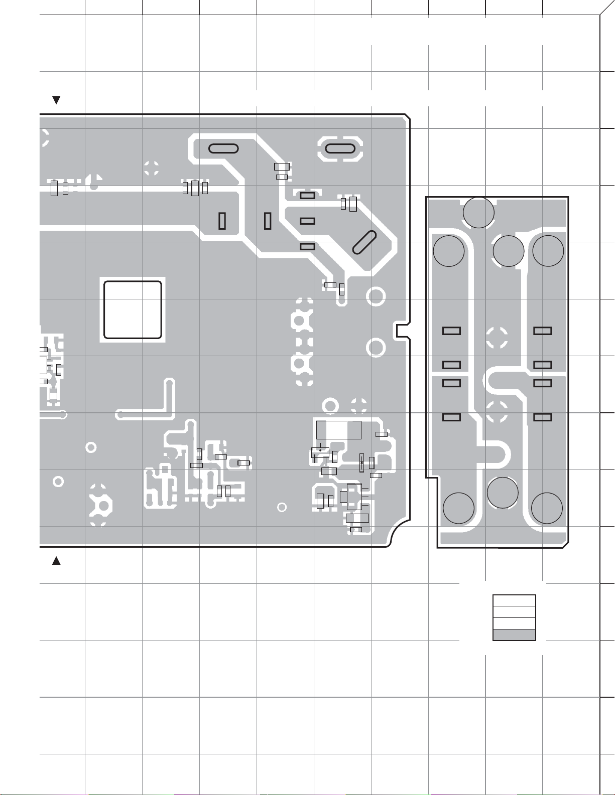
JKLMNOPQRS
C50
C49
C78
C79
C77
PC BOARD TKR-851
FINAL UNIT (X45-3742-71) Foil side view (J72-0911-09)
C115
C114
C116
C105
C117
R54
GND
Back up battery
+B2
GND
Main DC
+B1
1
2
3
4
5
6
52
3
1
1
C107
51
C106
R50
C98
7
8
C15
C18
R6
C19
R7
C10
Q9
C99
C113
C112
C104
IC2
+
C102
D10
I
G
O
C103
C100
C101
+B2
GND
+B1
J72-0911-09 (B/2)
9
10
Component side
Layer 1
Layer 2
11
Layer 3
Layer 4
Foil side
55
12
13
14

JKLMNOPQRSIHGFEDCBA
TKR-851 PC BOARD PC BOARD TKR-851
1
2
3
4
FINAL UNIT (X45-3742-71) Foil side view (J72-0911-09) FINAL UNIT (X45-3742-71) Foil side view (J72-0911-09)
C52
C53
C115
C114
C77
C50
C49
C78
C79
C116
C117
GND
Back up battery
+B2
GND
Main DC
+B1
5
C105
R54
6
R53
1
2
3
4
5
6
10
11
R52
34
IC1
6
1
C109
7
8
9
C91
C92
C93
C94
C95
C96
C97
J72-0911-09 (A/2)
R51
C108
C107
C106
7
R50
C98
8
C15
C18
R6
C19
R7
C10
Q9
C99
C113
C112
C104
IC2
+
C103
C102
G
O
D10
I
C100
C101
+B2
GND
+B1
J72-0911-09 (B/2)
9
10
Ref. No. Address
IC1 7J
IC2 9O
Q9 8O
D10 8O
Component side
Layer 1
Layer 2
Layer 3
Layer 4
11
Foil side
12
13
14
12
13
14

JIHGFEDCBA
1
TKR-851
1
PC BOARD
2
DISPLAY UNIT (X54-3330-21) Component side view (J72-0756-12)
3
VR601
4
5
NC
HK
6
MIG
GND
NC
MIC
PTT
J601
SB
1
IC504
8
10
11
D503
7
TX
J72-0756-12 B/2
8
S501
PF1
S502
PF2
S503
PF3
S504
PF4
9
1346
Q512
12
13
14
56

JKLMNOPQRS
D506
16
1
IC504 IC505
89
D507
16
1
89
PC BOARD TKR-851
DISPLAY UNIT (X54-3330-21) Component side view (J72-0756-12)
J72-0756-12 A/2
S507
POWER
D505
GRN RED
MAINDCBACK-
UP
1
2
3
4
5
6
03
D504
BUSY
7
8
S505
PF5
S506
PF6
Q514
16
43
Component side
Layer 1
Layer 2
9
Foil side
10
Ref. No. Address
IC504 6J
IC505 6L
11
Q512 10A
Q514 9P
D503 7J
D504 7M
D505 5R
12
D506 5J
D507 5L
57
13
14

JKLMNOPQRSIHGFEDCBA
TKR-851 PC BOARD
1
PC BOARD TKR-851
2
DISPLAY UNIT (X54-3330-21) Component side view (J72-0756-12) DISPLAY UNIT (X54-3330-21) Component side view (J72-0756-12)
J72-0756-12 A/2
3
VR601
4
5
D506
NC
HK
6
MIG
GND
NC
MIC
PTT
SB
J601
16
1
IC504 IC505
89
D507
16
1
89
S507
POWER
D505
GRN RED
MAINDCBACK-
UP
1
2
3
4
5
6
10
11
12
D503
7
TX
D504
BUSY
7
J72-0756-12 B/2
8
S501
PF1
S502
PF2
S503
PF3
S504
PF4
S505
PF5
S506
PF6
9
Q514
16
1346
Q512
43
Component side
Layer 1
Layer 2
Foil side
8
9
10
Ref. No. Address
IC504 6J
IC505 6L
11
Q512 10A
Q514 9P
D503 7J
D504 7M
D505 5R
12
D506 5J
D507 5L
13
14
13
14

JIHGFEDCBA
5
5
0
X
TKR-851
1
PC BOARD
2
DISPLAY UNIT (X54-3330-21) Foil side view (J72-0756-12)
J72-0756-12 A/2
3
4
5
6
7
8
Layer 1
9
Layer 2
BACKUP
R519
RED
Q510
R543
Q507
1
34
MAIN DC
GRN
6
Component side
Foil side
Q511
R544
R520
D513
R535
D514
R536
D510
R539
D511
Q525
R540
R538
1
89
IC502
16
D509
R537
R534
C511
D508
+
D512
C524
C525
C518
R526
C507
Q508
C506
R516
R509
R510
1
3
4
6
Q519
1
3
4
6
Q516
RED
T
C
R
1
IC5
4
1
3
CP504
446
3
1
Q523
6
34
1
CP503
Q521
C520
R606
G
D
S
1
6
334
Q503
I
O
G
C526
Q509
IC507
R542
R502R503
R541
R518
VLI
5M
GND
NC
NC
GND
CN501
PTT
MIG
MIC
SB
HK
4
6
Q504
R517
1
Q506
BUSY
RED
GRN
11
C517
+
R505
1
C501
VR501
Q502
+
R506
3
4
C523
C503
R507
Q501
61
6
Q524
Q522
I
IC506
G
R525
Q518
Q517
R508
O
61
1
6
D502
C502
+
34
34
C519
C522
CP502
CP501
+
C521
C516
C505
C504
D501
10
11
12
13
14
58
Ref. No. Address
IC501 9J
IC502 7D
IC503 9P
IC506 8I
IC507 8F
Q501 9I
Q502 9H
Q503 7F
Q504 7G
Q506 7G
Ref. No. Address
Q507 7B
Q508 8J
Q509 7F
Q510 6B
Q511 6C
Q513 9N
Q516 5J
Q517 5I
Q518 4I
Q519 4J
Ref. No. Address
Q521 5H
Q522 5I
Q523 4H
Q524 4I
Q525 6F
D501 9I
D502 9I
D508 7E
D509 8E
D510 6D
Ref. No. Address
D511 6D
D512 7E
D513 6C
D514 6D
D601 5R
D602 4R
D603 4R

JKLMNOPQRS
R509
R
PC BOARD TKR-851
1
2
DISPLAY UNIT (X54-3330-21) Foil side view (J72-0756-12)
CN601
HK
MIC
MIG
PTT
11
C602
1
3
4
6
1
3
4
6
Q516 Q519
R601
GNDNCSBNCGND5MVLI
C606
C603
D603
C601
R604
D602
D601
R605
NC
MIC
PTT
SB
HK
MIG
GND
NC
1
C607
3
4
5
6
516
R510
GRN
RED
TX
R524
C508
R511
1
8
IC501
45
R512
R513
C509
+
C510
R514
7
J72-0756-12 B/2
CN502
20
SB
NC
PSW
SB
GND
DAT
19
CLK
PTT/TXD
HK/RXD
STB1
SOEK1K2K4VLI
R529
K3K55C
MIC
MIG
12
R533
R523
C515
R530
Q513
1346
R531
C514
R532
R522
C512
16
1
IC503
C513
R521
9
8
8
9
10
11
59
12
13
14

JKLMNOPQRSIHGFEDCBA
TKR-851 PC BOARD PC BOARD TKR-851
1
2
DISPLAY UNIT (X54-3330-21) Foil side view (J72-0756-12) DISPLAY UNIT (X54-3330-21) Foil side view (J72-0756-12)
J72-0756-12 A/2
MIC
C602
R601
CN601
MIG
PTT
GNDNCSBNCGND5MVLI
C606
D603
C601
C513
R521
C603
R604
D602
D601
R605
NC
MIC
PTT
SB
HK
MIG
GND
NC
1
C607
3
HK
11
4
5
BACKUP
6
R519
7
8
Component side
Layer 1
9
Layer 2
Foil side
RED
Q510
R543
1
34
Q507
MAIN DC
GRN
6
Q511
R544
R520
D513
R535
D514
R536
D510
R539
C520
D511
R540
R538
1
89
IC502
16
D509
R537
R534
C511
D508
+
D512
C524
C518
Q525
C525
O
R526
G
S
1
334
Q503
G
C526
R606
D
R541
R542
Q509
6
R518
I
IC507
R502R503
VLI
5M
GND
NC
NC
GND
CN501
PTT
MIG
MIC
HK
SB
4
6
Q504
R517
1
Q506
BUSY
RED
11
1
GRN
Q523
Q521
+
C501
CP504
446
3
1
6
34
1
CP503
C517
R505
VR501
Q502
+
R506
3
3
4
C523
C503
R507
Q501
1
61
6
Q524
Q522
I
IC506
G
R525
Q518
Q517
R508
O
+
61
1
6
D502
C502
34
34
C519
C522
CP502
CP501
+
C521
C516
C505
C504
D501
C507
Q508
C506
R516
R509
R510
3
4
3
4
1
6
Q519
1
6
Q516
GRN
RED
TX
R524
C508
R511
1
8
IC501
45
R512
R513
C509
+
C510
R514
J72-0756-12 B/2
CN502
20
SB
NC
PSW
SB
GND
DAT
19
CLK
PTT/TXD
HK/RXD
STB1
SOEK1K2K4VLI
R529
K3K55C
MIC
MIG
12
R533
R523
C515
R530
Q513
1346
R531
C514
R532
R522
C512
16
1
IC503
9
8
1
2
3
4
5
6
7
8
9
10
11
12
13
14
Ref. No. Address
IC501 9J
IC502 7D
IC503 9P
IC506 8I
IC507 8F
Q501 9I
Q502 9H
Q503 7F
Q504 7G
Q506 7G
Ref. No. Address
Q507 7B
Q508 8J
Q509 7F
Q510 6B
Q511 6C
Q513 9N
Q516 5J
Q517 5I
Q518 4I
Q519 4J
Ref. No. Address
Q521 5H
Q522 5I
Q523 4H
Q524 4I
Q525 6F
D501 9I
D502 9I
D508 7E
D509 8E
D510 6D
Ref. No. Address
D511 6D
D512 7E
D513 6C
D514 6D
D601 5R
D602 4R
D603 4R
10
11
12
13
14

JIHGFEDCBA
TKR-851
1
PC BOARD
TX-RX UNIT (X57-6962-70) (A/2) Component side view (J72-0924-09 A/2)
2
3
L2
4
5
6
7
8
PSW
3
B
CN15
CN18
1
IC9
20
R65
C60
R169
C74
2
CN4
C216
R54
R61
C66
R60
C217
C67
R57
Q26
R70
C213
C51
R46
C214
C48
R44
R45
L16L17
L19
D2
L18
1
E
B
L20
CF1
WIDE
CF2
NARROW
R50
C58
C64
C53
C59
X1
1
10 11
R62
R63
L24
XF1
XF2
L4
NARROW
WIDE
L5
1
2
CN2
R41
C37
D1
A9
L14 L15
10
11
12
13
FCR
DT
Q27
SOE
STT
NC
SB
SB
SB
SB
NC
SRR
TX
36
8C
35
8C
MO
R69
Q4
R181
2
DET
1
NC
GND
NC
RSSI
ASQ
R182
SC
R142
DP
CP
R141
R140
EPR
LDRDTSTB
EPT
LDT
R139
R138
CN14
CK
R137
LD2
FWD
PSW
BUP
MB
SOE
TMP
GNDMOGND
GND
QS
9
K1
IC4
IGO
Ref. No. Address
IC4 11B
IC5 10I
IC9 7D
IC10 11I
SB
Ref. No. Address
Q4 9F
Q16 10K
Q17 10K
Q26 8E
8CR
Ref. No. Address
Q27 9F
D1 7J
D2 7F
C76
+
5CR
QS
CK
STB4
F1
C161
C173
C160
C172
LD2
IC5
I
FCT
+
I
G
G
IC10
9V
O
C158
C159
O
C174
+
14
60

JKLMNOPQRS
L5
2
CN2
PC BOARD TKR-851
1
TX-RX UNIT (X57-6962-70) (A/2) Component side view (J72-0924-09 A/2)
CN16
GNDNC8TPCFAS
1
C125
+
TP102
TX CV
8CT
C137
CN1
1
L33
R31
R32
R30
C14
C15
+
C139
+
GND1
STT
8CL
CV
9CL
MO
PDT
BUP
TMP
8
A2 : TX VCO (X58-481)
CN19
GND2
VO
FIN
5C
LDT
EPT
DP
CP
REF
2
3
4
5
6
R41
C37
D1
A1
FCT
CP
CP
EPT
LDT
7
R11
R10
R13
+
C158
9V
+
C159
C174
C171
A10
Q17
R128
Q16
B
R129
CN3
+
E
C
C147
C144
C124
+
TP101
RX CV
8CR
C136
+
C138
+
GND1
SRR
8CL
CV
9CL
NC
A3 : RX VCO (X58-480)
LDR
EPR
CP
DP
GND2
VO
FIN
5C
LDR
EPR
DP
CP
REF
J72-0924-09 A/2
8
9
10
11
Component side
Layer 1
Layer 2
Layer 3
Layer 4
Foil side
12
13
61
14

JKLMNOPQRSIHGFEDCBA
TKR-851 PC BOARD
1
TX-RX UNIT (X57-6962-70) (A/2) Component side view (J72-0924-09 A/2)
2
3
L2
4
5
6
7
8
PSW
3
B
CN15
CN18
1
IC9
20
R65
C60
R169
C74
2
CN4
C216
R54
R61
C66
R60
C217
C67
R57
Q26
C213
R70
C51
R46
C214
C48
R44
R45
L16L17
L19
D2
L18
1
E
B
L20
CF1
WIDE
CF2
NARROW
R50
C58
C64
C53
C59
X1
1
10 11
R62
R63
L24
XF1
XF2
L4
NARROW
WIDE
PC BOARD TKR-851
1
TX-RX UNIT (X57-6962-70) (A/2) Component side view (J72-0924-09 A/2)
CN16
GNDNC8TPCFAS
1
L5
CN1
1
2
L33
R32
R31
R30
A1
R11
R10
R13
CN2
R41
C37
D1
A9
L14 L15
C14
C15
A10
8CT
C137
C139
C125
+
TP102
TX CV
+
+
GND1
STT
8CL
CV
9CL
MO
PDT
BUP
TMP
8
A2 : TX VCO (X58-481)
CN19
FCT
GND2
VO
FIN
5C
LDT
EPT
DP
CP
REF
CP
CP
EPT
LDT
GND2
VO
2
3
4
5
6
7
8
10
11
12
13
FCR
DT
Q27
SOE
STT
NC
SB
SB
SB
SB
NC
SRR
TX
36
8C
35
8C
MO
R69
Q4
R181
2
DET
1
NC
NC
GND
ASQ
R182
RSSI
SC
R142
DP
CP
R141
R140
EPR
LDRDTSTB
EPT
LDT
R139
R138
CN14
CK
FWD
R137
LD2
BUP
PSW
TMP
SOE
QS
MB
GND
GNDMOGND
9
K1
IC4
IGO
Ref. No. Address
IC4 11B
IC5 10I
IC9 7D
IC10 11I
SB
Ref. No. Address
Q4 9F
Q16 10K
Q17 10K
Q26 8E
8CR
Ref. No. Address
Q27 9F
D1 7J
D2 7F
C76
+
5CR
QS
CK
STB4
F1
C161
C173
C160
C172
LD2
I
IC5
FCT
+
I
O
G
G
IC10
9V
C158
C159
O
C174
+
C171
Q17
R128
Q16
B
R129
E
C
+
C147
CN3
C144
C124
+
TP101
RX CV
8CR
C136
+
C138
+
GND1
SRR
8CL
CV
9CL
NC
A3 : RX VCO (X58-480)
LDR
DP
EPR
Layer 1
Layer 2
Layer 3
Layer 4
CP
Component side
Foil side
FIN
5C
LDR
EPR
DP
CP
REF
J72-0924-09 A/2
9
10
11
12
13
14
14

JIHGFEDCBA
3
B
3
3
TKR-851
1
TX-RX UNIT (X57-6962-70) (A/2) Foil side view (J72-0924-09 A/2)
2
R95
FIN
5C
LDT
EPT
DP
CP
REF
FIN
5C
LDR
EPR
DP
CP
REF
GND2
VO
R174
GND2
VO
R175
R151
R152
R153
R154
R155
R156
R157
R158
C90
C94
R168
R179
C89
L32
L42
C115
L31
R162
C117
C29
C28
R82
C116
3
4
C234
5
6
7
8
9
10
Q11
R96
R79
C114
R92
C91
C92
R94
C93
R93
PC BOARD
R136
C101
C99
R143
R106
R109
45
R18
R19
1
C231
X3
C95
R97
R98
Q8
C97
R100
C98
R99
C96
C179
L28
R101
IC1
8
R78
R91
L25
X2
+
D8
R135
R17
R20
R77
+
+
+
L26
C84
C164
C25
C24
+
C81
C80
R134
R144
Q9
R73
R76
C166
R148
R145
C167
C82
R74
C83
R75
+
C106
5
8
C146
Q23
C178
IC2
+
C177
C100
R102
R103
C102
R107
C104
R105
4
1
C145
L35
C204
L36
C191
B
IC11
O
O
C205
C
R130
R131
L27
G
L37
C192
G
B
C
E
C206
E
I
Q10
IC3
I
L38
C193
Q18
L39
C207
Q19
C105
C148
C208
C194
+
C175
L40
C195
C150
C176
R114
R113
C149
C152
GND1
STT
8CL
CV
9CL
MO
C87
+
GND1
SRR
8CL
CV
9CL
NC
R90
C223
C86
R87
C233
C232
C129
C123
C120
R127
C143
L30 L29
C128
C122
C121
C88
R88
C142
R126
Q15
R125
C111
C126
Q14
R124
C127
C133
C135
C141
R121
R122
C131
C109
+
R120
R123
C130
C132
C134
C140
+
Q13
C107
Q12
A11
C13
L11
C211
R9
R8
R34
C212
R33
C30
C31
L10
C33
C32
R35
C34
L12
R36
R37
L1
Q2
R
R
C3
11
12
13
14
J72-0924-09 A/2
62
Ref. No. Address
IC1 4C
IC2 10D
IC3 10E
IC6 9K
IC7 9L
IC11 6E
Ref. No. Address
Q1 3N
Q2 7J
Q3 7O
Q5 9N
Q6 9M
Q7 10O
Ref. No. Address
Q8 8C
Q9 8D
Q10 7E
Q11 3B
Q12 9G
Q13 4G
Ref. No. Address
Q14 10G
Q15 5G
Q18 5E
Q19 5E
Q23 3D
Q24 9R
Ref. No. Address
Q25 9R
D3 7Q
D4 8Q
D5 11O
D7 9S
D8 3D
Ref. No. Address
D11 10N
D12 9Q
D13 11N

JKLMNOPQRS
31
C33
C32
R35
C34
R34
L12
R36R37
L13
R39
R38
C36
PC BOARD TKR-851
1
TX-RX UNIT (X57-6962-70) (A/2) Foil side view (J72-0924-09 A/2)
2
R5
C4
Q1
E
R3
C
B
L3
C210
C41
R43
C45
C44
Q2
E
B
C
R40
C40
R42
C39
C38
C42
C43
C163
C7
C8
C5
C199
C50
C47
C46
C49
R2
L34
R51
R48
C52
R178
R150
R163
L6
Q3
R164
C57
C3
L23
R49
L21
C54
C197
R14
C61
C65
C198
R83
+
C69
C70
R171
R160
R161
C63
C56
R53
R56
C68
R47
D3
D4
L1
C55
R52
R55
C62
R58
3
4
5
6
7
8
IC7
9
R71
Q5
D11
TH1
R72
C218
D13
C79
R67
C75
C73
R66
Q7
C77
C78
L43
R68
R176
D5
+
C72
C71
C190
Q6
C184
C189
C185
8
D12
R165
R166
+
C151
C153
C157
C156
Component side
Q25
Q24
C162
9
D7
10
11
12
1
8
IC6
9
C155
C154
16
16
1
+
Layer 1
Layer 2
Layer 3
Layer 4
Foil side
13
63
14

JKLMNOPQRSIHGFEDCBA
TKR-851 PC BOARD
1
TX-RX UNIT (X57-6962-70) (A/2) Foil side view (J72-0924-09 A/2)
2
R136
C101
R106
C231
R143
C95
R97
R98
C97
R100
C98
R99
R18
R19
D8
+
R135
R17
R20
R77
+
+
L26
C84
+
C164
+
C81
10
11
R95
Q11
FIN
5C
LDT
EPT
DP
CP
REF
GND2
VO
R174
R151
R152
R153
R154
C94
R168
R179
C89
L42
L31
C29
C28
R82
C115
C114
R96
R79
C96
C179
R101
8
IC1
R78
L28
C99
X3
R109
45
1
3
4
C234
5
6
7
R92
C116
C91
C92
R94
C93
R93
R91
Q8
L25
X2
R162
GND2
8
9
FIN
5C
LDR
EPR
DP
CP
REF
VO
R175
R155
R156
R157
R158
C90
C117
L32
J72-0924-09 A/2
C25
C24
C80
R134
R144
R145
Q9
R73
R76
C166
R148
C167
C82
R74
C83
R75
+
C106
5
8
C146
Q23
C178
IC2
+
C177
C100
R102
R103
C102
R107
C104
R105
4
1
C145
L35
C204
L36
C191
B
IC11
O
O
C205
C
R130
R131
L27
G
L37
C192
G
B
C
E
C206
E
I
Q10
IC3
I
L38
C193
Q18
L39
C207
Q19
C105
C148
C194
+
C175
C208
C195
C150
C176
R114
R113
C149
L40
C152
GND1
STT
8CL
CV
9CL
MO
C87
+
GND1
SRR
8CL
CV
9CL
NC
R90
C223
C86
R87
C233
C232
C129
C123
C120
R127
C143
L30 L29
C128
C122
C121
C88
R88
C142
R126
Q15
R125
C111
Q14
C126
R124
C127
C133
C135
C141
R121
R122
C131
C109
+
R120
R123
C130
C132
C134
C140
+
Q13
C107
Q12
A11
C13
R9
L11
R8
R33
C30
C211
C31
C212
L10
C33
C32
R35
C34
R34
L12
R36
R37
L13
R39
R38
C36
Q2
PC BOARD TKR-851
1
TX-RX UNIT (X57-6962-70) (A/2) Foil side view (J72-0924-09 A/2)
2
R5
C4
Q1
E
R3
C
B
L3
C190
C189
Q6
C7
C8
C184
C185
C47
C46
C5
C199
C50
C49
Q5
D11
R71
C210
C41
R43
C42
C39
E
B
C
R40
C38
C43
C40
R42
C163
1
8
IC6
9
C155
C154
16
16
1
+
9
IC7
8
C45
C44
TH1
R72
R2
L34
R51
C218
R48
C52
R178
D13
R150
R163
L6
Q3
R164
C79
R67
C75
C57
C63
C56
R53
R56
C68
+
D12
C151
C157
R47
D3
D4
L1
R165
R58
C153
C156
C55
R52
R55
C62
R166
Q25
Q24
C162
D7
C3
R171
L23
C61
C198
+
C65
L43
R68
C71
R83
C69
C70
R160
R161
C54
R49
R14
C197
L21
C73
R66
Q7
C77
C78
R176
D5
+
C72
3
4
5
6
7
8
9
10
11
12
13
14
Ref. No. Address
IC1 4C
IC2 10D
IC3 10E
IC6 9K
IC7 9L
IC11 6E
Ref. No. Address
Q1 3N
Q2 7J
Q3 7O
Q5 9N
Q6 9M
Q7 10O
Ref. No. Address
Q8 8C
Q9 8D
Q10 7E
Q11 3B
Q12 9G
Q13 4G
Ref. No. Address
Q14 10G
Q15 5G
Q18 5E
Q19 5E
Q23 3D
Q24 9R
Ref. No. Address
Q25 9R
D3 7Q
D4 8Q
D5 11O
D7 9S
D8 3D
Ref. No. Address
D11 10N
D12 9Q
D13 11N
Component side
Layer 1
Layer 2
Layer 3
Layer 4
Foil side
12
13
14

JIHGFEDCBA
L
TKR-851
1
PC BOARD
2
TX-RX UNIT (X57-6962-70) (B/2) Component side view (J72-0924-09 B/2)
C623
5-TONE
D600
C825
C806
R604
Q612
+
R605
R836
C780
C786
O
IC624
G
I
G
3
I
G
O
4
5
IC627
IC601
+
C785
L601
L604
C613
R603
C826
G
I
O
6
CN600
20MIC
L606
5CK5K3
MIG
VLIK4K2K1SOE
19
HK/RXD1
PTT/TXD1
I
IC628
C769
O
+
C766
SB
NC
CLK
PSW
STB1
DAT
GND
SB
12
C600
3.3D
R601
C781
10
11
12
7
C644
+
C645
8
+
C646
9
J72-0924-09 B/2
Ref. No. Address
IC601 6A
IC602 7K
IC605 6K
IC607 8O
IC623 8K
IC624 4G
IC625 4K
IC627 4A
Ref. No. Address
IC628 3G
IC629 4R
IC630 4N
Q607 8L
Q608 9L
Q612 5B
Q613 8M
Q614 9M
C691
Ref. No. Address
D600 4B
D614 6M
D618 6M
D621 7M
D626 4M
D629 6N
TRST GND NC GND GND GND EMU1
TMS TD1 DVDD TD0 TCK TCK EMU0
1
13
14
64

JKLMNOPQRS
R601
EMU1
EMU0
C781
L607
R653
I
G
TXO
TXI
RXO
AC
BC1
BC2
BC3
BC4
CN601
PTI
CLRC
RXI
PTO
NC
GND
O
1
14
+
IC625
C770
1
1
8
9
16
C765
C767
DEI
8
IC602
IC623
PC BOARD TKR-851
TX-RX UNIT (X57-6962-70) (B/2) Component side view (J72-0924-09 B/2)
1
+
SPI
D629
L608
RSI
RD
+
SPG
C800
C817
12
SPG
+
C663
+
+
C823
R812
C814
+
SB
C657
R781
+
R841
8
1
R676
C652
R742
C649
R674
IC607
R669
R672
C789
C798
C811
30NC
29
C788
R764
R675
++
C760
45
R671
+
+
+
NC
NC
EMON
NCNCRXD2
TXD2
R765
C790
C772
ANI
C818
C819
C820
5C
NC
EPTT
CN606
AI1
AI2
AI3DGTDTARDRARXG
C809
C812
C816
R771
R751
C827
TXG
C807
IO1
R768
C804
IO2
R766
C762
IO3
R760
10
C802
IO4
IC629
C796
C799
IO5
IO6
SPM
C792
R750
R749
R752
++
C794
21
NC
NC
C774
C773
R654
IC605
R658
CP600
16
9
16
9
8
1
R657
R655
DEO
R607
R609
CP601
C642
Q607
R840
Q608
R611
D621
R839
R612
C803
R785
R613
Q613
Q614
D614
1
SB
CN603
L613
1
AO5
R793
C808
D626
SB
AO4
L612
AO3
L611
GND
D618
SPO
C810
4
GND
SPO
CN604
CN610
CN609
8C
IC630
C801
R789
AO2
C813
CN605
SPO
1
SB
G
O
C795
C805
AO1
2
I
SPG
C681
CN608
RSSI
CN607
RSSI
C828
1
2
3
4
5
6
7
8
9
Component side
Layer 1
Layer 2
Layer 3
Layer 4
Foil side
10
11
12
13
65
14

JKLMNOPQRSIHGFEDCBA
TKR-851 PC BOARD
1
2
TX-RX UNIT (X57-6962-70) (B/2) Component side view (J72-0924-09 B/2)
C623
C825
5-TONE
D600
C806
R604
Q612
+
R605
R836
C644
+
C645
+
C691
C646
C780
C786
O
IC624
G
I
G
3
I
G
O
4
5
IC627
IC601
+
C785
L601
L604
C613
R603
C826
G
I
O
6
7
8
9
J72-0924-09 B/2
PC BOARD TKR-851
1
2
TX-RX UNIT (X57-6962-70) (B/2) Component side view (J72-0924-09 B/2)
TXG
C807
IO1
R768
C804
IO2
R766
C762
IO3
R760
1
10
C802
IO4
IC629
C796
C799
IO5
IO6
SPM
C792
R750
R749
R752
++
C794
21
NC
NC
C773
C774
CN608
RSSI
CN607
RSSI
C828
3
4
5
6
7
8
9
CN600
20MIC
I
IC628
C769
O
+
C766
5CK5K3
HK/RXD1
PTT/TXD1
MIG
VLIK4K2K1SOE
19
L606
TRST GND NC GND GND GND EMU1
TMS TD1 DVDD TD0 TCK TCK EMU0
1
SB
NC
CLK
PSW
STB1
DAT
GND
SB
12
C600
3.3D
R601
C781
L607
R653
G
TXO
TXI
RXO
AC
BC1
BC2
BC3
BC4
CN601
PTI
CLRC
RXI
PTO
NC
GND
C770
I
O
+
C767
1
1
8
9
16
C765
8
IC602
IC623
R654
DEI
IC605
R658
CP600
16
16
9
8
1
R657
IC625
1
14
9
R655
DEO
R607
CP601
R609
C642
Q607
R840
Q608
R611
D621
R839
R612
R613
C803
R785
Q614
D614
Q613
1
SB
CN603
L613
1
AO5
R793
C808
D626
SB
AO4
L612
AO3
L611
GND
D618
SPO
C810
CN609
4
GND
SPO
CN604
CN605
8C
IC630
C801
R789
AO2
C813
SPO
1
CN610
SB
I
G
O
C795
C805
AO1
SPG
2
C681
+
SPI
D629
L608
RSI
RD
+
SPG
C800
C817
12
SPG
+
C663
+
+
C823
R812
C814
+
SB
C657
R781
R841
8
1
R676
C652
+
R742
C649
R674
IC607
45
R669
R672
C788
R675
C760
R671
ANI
C789
+
C798
+
C811
+
30NC
NC
NC
EMON
NCNCRXD2
TXD2
29
R765
R764
C790
C827
C772
++
C818
C819
C820
5C
NC
EPTT
CN606
AI1
AI2
AI3DGTDTARDRARXG
C809
C812
C816
R751
R771
10
11
12
13
14
Ref. No. Address
IC601 6A
IC602 7K
IC605 6K
IC607 8O
IC623 8K
IC624 4G
IC625 4K
IC627 4A
Ref. No. Address
IC628 3G
IC629 4R
IC630 4N
Q607 8L
Q608 9L
Q612 5B
Q613 8M
Q614 9M
Ref. No. Address
D600 4B
D614 6M
D618 6M
D621 7M
D626 4M
D629 6N
Component side
Layer 1
Layer 2
Layer 3
Layer 4
Foil side
10
11
12
13
14

JIHGFEDCBA
3
1
2
7
6
T
G
TKR-851
1
PC BOARD
2
TX-RX UNIT (X57-6962-70) (B/2) Foil side view (J72-0924-09 B/2)
G
R762
Q609
R753
C815
D611
C723
R709
R714
45
C722
D
Q610
C783
C791
R767
R802
C746
C736
C670
+
C692
R736
R732
C744
S
+
C739
R737
C758
R681R682
R741
R728
1
45
IC619
++
C701
1
12 13
R740
R729
8
IC615
IC611
8
R679
R739
C743
+
C720
45
1
R738
R735
C841
24
Q605
IC621
R790
D606
C784
C787
R758
R754
Q606
IC622
R745
D608
R791
R795
R763
C793
C797
R774
Q611
C778
+
D628
1
34
5
R815
R744
C764
R747
34
1
5
R743
D619
D615
R798
C729
R809
D607
R807
R810
R803
R799
C730
+
R808
R804
C822
C821
TH700
D609
8
1
R719
R843
R806
R721
R805
R715
IC617
R713
+
3
4
5
D620
D623
R775
R777
R782
R776
R778
6
7
D616
+
C775
C777
+++
8
8
IC620
9
9
D612
R780
R779
R773
C779
C763
C761
R772
R786
C776
1
16
D610
R783
D622
R787
R794
C740
C715
C705
R685R686
R811
R842
R684
C690
8CSBSBNCGNDMOGND
2
8CNCSBSBQS
1
C602
C605
D627
C648
IC608
C706
C700
C679
+
R710
TMP
BUP
FWDCKLDT
EPTCPSC
ASQNCNC
GNDMBSOE
PSW
LD2
STBDTLDR
EPRDPRSSI
C685
IC610
G
I
O
16
8
C684
R683
R680
C782
IC626
C768
5
+
GND
34
C721
CN602
R844
R668
R673
TH701
+
C647
R670
++
C703
C704
R717
R718
C724
C643
34
51
1
C639
C698
C697
R708
R707
R690
IC614
819
C728
IC616
415
+
+
C726
DET
35
+
R712
R722
36
C771
R608
R678
+
C662
C725
R610
Q615
IC612
R689
R694
R696
R698
1345
89
R693
C707
R695
C695
C708
C696
C709
C711
IC613
1
16
L605
EMU1
EMU0
D
R69
R69
R69
R81
Q
+
+
+
C693
C694
C710
C712
10
11
12
13
14
66
Ref. No. Address
IC600 4O
IC603 9N
IC604 6Q
IC606 4M
IC608 6G
IC609 9Q
IC610 6H
IC611 9F
Ref. No. Address
IC612 8J
IC613 8J
IC614 8H
IC615 8F
IC616 9H
IC617 8D
IC618 7L
IC619 6F
Ref. No. Address
IC620 8B
IC621 5C
IC622 5C
IC626 7H
IC631 3N
IC632 3M
Q600 4Q
Q601 3K
Ref. No. Address
Q602 3J
Q603 4K
Q604 8L
Q605 5C
Q606 4C
Q609 4E
Q610 3E
Q611 4D
Ref. No. Address
Q615 6I
D606 7C
D607 7C
D608 6C
D609 7D
D610 6B
D611 6E
D612 6B
Ref. No. Address
D615 6D
D616 7B
D619 6C
D620 7A
D622 7B
D623 6A
D627 4G
D628 4D

JKLMNOPQRS
R695
IC613
R693
C707
C695
C708
C696
C709
C711
L605
PC BOARD TKR-851
1
2
TX-RX UNIT (X57-6962-70) (B/2) Foil side view (J72-0924-09 B/2)
Q601
Q602
S
D
R691
R692
R697
R813
+
+
C693
G
C713
C717
C718
37
Q603
R702
+
R700
36
R720
R723
R724
C731
C732
+
C733
IC618
C842
C741
C742
+
R726
R832
R831
C694
+
72
C710
73 108
116
C727
R704
R731
R734
TRSTGNDNCGNDGNDGNDEMU1
Q604
G
S
C735
C738
D
C734
R733
R727
C737
C712
C714
C719
C716
+
R701
R705
R703
R699
TMSTD1DVDDTD0TCKTCKEMU0
R833
C745
+
X601
C840
1
C839
R822
144
109
IC632
8
R830
24
C843
C835
24
45
1
IC606
IC603
R826
C833
C749
C750
+
C747
C759
+
+
C752
C748
+
C755
C751
R730
R829
C837C838
1213
1
C754
C757
C753
C756
1213
1
C836
R828
R688
C824
R687
C832
C844
C831
IC631
R827
R825
C834
8
CP603
R824
45
1
R616
R606
R640
R642
L603
R644
R614
R630
R631
R622
R637
R643
R645
R646
R667
R662
C830
C829
R821
R823
C616
R627
R635
CP606
CP609
R639
R641
R647
R648
R649
R650
R651
R665
R663
R818
R819
8
R834
R666
R820
IC600
R837
R664
R814
R626
25
R625
R624
R621
R623
R633
R620
R634
R619
C635
C638
45
1
C851
26
CP607
IC604
50
51 75
R652
CP619
CP618
CP617
CP616
1
IC609
16
X600
C634
R629
Q600
R600 R602
C614
CP615
D
C629
CP614
S
G
1
100
76
CP613
R615
CP620
R817
CP604CP605
R638
C641
+
32
17
R618
C640
CP608
L602
CP610
CP611
R661
CP612
R660
R659
R656
J72-0924-09 B/2
3
4
5
6
7
8
L600
9
Component side
Layer 1
Layer 2
Layer 3
Layer 4
Foil side
10
11
12
13
67
14

JKLMNOPQRSIHGFEDCBA
TKR-851 PC BOARD
1
2
TX-RX UNIT (X57-6962-70) (B/2) Foil side view (J72-0924-09 B/2)
G
R762
Q609
R753
C815
D611
C723
R709
R714
45
C722
D
Q610
C783
C791
R767
R802
C746
C736
C670
+
C692
R736
R732
C744
S
+
C739
R737
C758
R681R682
R741
R728
1
45
IC619
++
C701
1
12 13
R740
R729
8
IC615
IC611
8
R679
R739
C743
+
C720
45
1
C740
R738
R735
C841
24
Q605
IC621
R790
D606
C784
C787
R758
R754
Q606
34
IC622
R745
D608
R791
R795
5
R763
R774
1
5
34
1
R798
C729
C764
R809
C793
C778
+
R744
R747
R810
D607
R743
D619
R799
+
C797
R815
D628
R807
R803
C730
R808
Q611
D615
R804
C822
C821
TH700
8
1
R719
R843
R806
D609
R721
R805
R715
IC617
R713
+
3
4
5
D620
D623
R775
R777
R782
R776
R778
R780
6
7
D616
+
C775
C777
+++
8
8
IC620
9
9
D612
R779
R773
C779
C763
C761
R772
R786
C776
1
16
R783
D622
D610
R787
R794
8CSBSBNCGNDMOGND
2
8CNCSBSBQS
1
C605
R811
C715
C705
R842
R684
R685R686
+
C690
R710
TMP
BUP
FWDCKLDT
EPTCPSC
ASQNCNC
36
GNDMBSOE
PSW
LD2
STBDTLDR
EPRDPRSSI
GND
C782
IC626
C768
C684
R683
5
R680
+
34
C721
DET
35
+
R712
R722
R608
R678
+
C662
C771
C725
CN602
C602
D627
R844
R668
R673
TH701
+
C643
C647
34
51
1
C648
IC608
C706
C700
C679
R670
++
C698
C697
C703
+
+
C704
R708
R707
R717
C726
R718
C724
IC610
C639
G
I
O
R690
IC614
819
C728
IC616
415
C685
16
8
R610
Q615
IC612
R689
R694
R696
R698
1345
PC BOARD TKR-851
1
2
TX-RX UNIT (X57-6962-70) (B/2) Foil side view (J72-0924-09 B/2)
Q601
Q602
S
D
G
C717
C718
C713
R691
R692
R697
R693
R813
C707
R695
C695
C708
C696
C709
C711
1
89
IC613
16
L605
+
+
+
C712
C693
C694
C710
37
72
C714
C719
C716
Q603
R702
+
R700
36
73 108
+
R701
R705
R703
R699
R720
R704
R723
C727
R731
R734
TRSTGNDNCGNDGNDGNDEMU1
TMSTD1DVDDTD0TCKTCKEMU0
R724
IC618
G
C738
C731
C732
+
Q604
S
C735
C733
D
C734
R733
C842
C741
C742
R727
C737
+
R726
R832
R831
C838
R833
C745
+
X601
C840
1
C839
R822
144
109
IC632
8
R830
24
C843
24
C835
IC606
45
1
C749
C750
C747
C752
C748
C751
IC603
R826
C833
+
C759
+
+
+
C755
R730
1213
1
C754
C757
C753
C756
1213
R829
C836
R828
C837
R688
C824
R687
1
C832
C844
C831
IC631
R827
R825
C834
8
CP603
R824
45
1
R616
R606
R640
R642
L603
R644
R614
R630
R631
R622
R637
R643
R645
R646
R667
R662
C830
C829
R821
R823
C616
R627
R635
CP606
CP609
R639
R641
R647
R648
R649
R650
R651
R665
R663
R818
R819
8
R834
R666
R820
IC600
R837
R664
R633
R624
R625
CP618
R621
R623
R620
CP617
R814
R634
R619
IC604
C635
C638
CP616
IC609
45
1
C851
R626
25
26
CP607
50
51 75
CP619
R652
1
16
X600
C634
R629
Q600
R600 R602
C614
CP615
D
C629
CP614
S
G
1
100
76
CP613
R615
CP620
R817
CP604CP605
R638
C641
+
32
17
R618
C640
CP608
CP612
L602
CP610
CP611
R661
R660
R659
R656
J72-0924-09 B/2
3
4
5
6
7
8
L600
9
10
11
12
13
14
Ref. No. Address
IC600 4O
IC603 9N
IC604 6Q
IC606 4M
IC608 6G
IC609 9Q
IC610 6H
IC611 9F
Ref. No. Address
IC612 8J
IC613 8J
IC614 8H
IC615 8F
IC616 9H
IC617 8D
IC618 7L
IC619 6F
Ref. No. Address
IC620 8B
IC621 5C
IC622 5C
IC626 7H
IC631 3N
IC632 3M
Q600 4Q
Q601 3K
Ref. No. Address
Q602 3J
Q603 4K
Q604 8L
Q605 5C
Q606 4C
Q609 4E
Q610 3E
Q611 4D
Ref. No. Address
Q615 6I
D606 7C
D607 7C
D608 6C
D609 7D
D610 6B
D611 6E
D612 6B
Ref. No. Address
D615 6D
D616 7B
D619 6C
D620 7A
D622 7B
D623 6A
D627 4G
D628 4D
Component side
Layer 1
Layer 2
Layer 3
Layer 4
Foil side
10
11
12
13
14

JIHGFEDCBA
TKR-851
1
RX VCO UNIT (X58-4800-10)
Component side view (J72-0751-02)
2
3
4
5
6
J72-0751-02 A/2 J72-0751-02 A/2
R364
9CL
NC
CV
6
Q354
PC BOARD
1
VO
C376
CN350
GND
SRR
8CL
1
2
GND
CN351
RX VCO UNIT (X58-4800-10)
Foil side view (J72-0751-02)
1
2
CN351
GND
C360
C354
R356
C368
Q350
VO
C372
L360
TC350
C370
S
D
C366
R360
D350
L352
C379
R362
Q352
C374
C364
G
L356
C362
L354
D352
L353
GND
1
L358
C356
SRR
L362
Q355
R351
R353
C351
R354
C383
8CL
R368
R365
R355
C386
C350
R352
CV
C377
R366
C378
R367
R358R359
L359
9CL
C375
C365
C355
D353
L355
L351
C363
NC
6
L361
C369
L357
D351
R350
R363
R357
C371
C367
TC351
L350
CN350
C373
S
G
D
C358C359
C361
C357
R361
Q353
Q351
10
11
12
+
+
LDR
C311
R320
C309
C324
5C
R300
R319
C310
1
FIN
C325
R308
R311
CN300
C307
C317
C314
C312
R315
C322
R322
C319
L302
L301
R321
L303
1
FIN
Q302
C321
5C
10 11
R318
C323
LDR
R305
R301
C305
C304
EPR
IC300
R314
R304
DT
R303
1
20
R317
R316
Q301
CP
R302
7
REF
CN300
Q300
7
7
REF
C306
EPR
DT
CP
8
9
C308
L300
R310
R306
R309
R312
C315
R313
+
C318
+
C320
J72-0751-02 B/2 J72-0751-02 B/2
13
14
Ref. No. Address
Q354 3C
68
Component side
Layer 1
Layer 2
Foil side
Ref. No. Address
IC300 10G
Q300 11H
Q301 11H
Q302 8G
Q350 4F
Ref. No. Address
Q351 4H
Q352 3F
Q353 3H
Q355 3G
D350 6F
Ref. No. Address
D351 6H
D352 6G
D353 6H
Component side
Layer 1
Layer 2
Foil side

ABCDE FGH I J
PC BOARD
TX VCO UNIT (X58-4810-10)
Component side view (J72-0752-12)
J72-0752-12 A/2 J72-0752-12 A/2
D355
R375
C381
R374
MO
6
9CL
R373
C380
R372
GND
STT
8CL
CV
1
D354
CN350
2
1
CN351
GND
VO
TX VCO UNIT (X58-4810-10)
Foil side view (J72-0752-12)
1
2
CN351
GND
R376
C360
C354
C368
Q350
C359
VO
L360
TC350
C370
S
D
C366
D350
L352
G
L356
CN350
C379
C374 C375
C364
L358
C362
L354 L355
D352
L353
GND
1
L362
C356
STT
Q355
R354
R351
R353
C351
C383
8CL
R358R359
C352
R368
R365
R355
C350
R352
CV
C377
R366
C378
R367
C382
C365
L359
C355
D353
9CL
L361
C369
L357
C363
D351
L351
R350
MO
6
TKR-851
R377
C371
S
Q351
G
D
C367
TC351
C358
C361
C357
L350
C353
1
2
3
4
5
6
REF
7
C306
L301L302
R321
L303
1
FIN
Q302
C321
5C
10 11
R318
C323
LDR
R305
R301
C305
C304
EPT
R304
IC300
L306
R314
L307
C329
5C
R300
R319
C310
FIN
1
C325
R311
R308
CN300
R315
C322
R322
C319
C317
C314
C312
C307
LDR
EPT
DT
CP
R313
C308
C330
R310
R309
+
R320
+
C309
C311
C324
+
+
L305
L300
R306
C318
C320
R312
C315
DT
1
20
R303
R317
R316
L304
Q301
CP
R302
7
REF
Q300
J72-0752-12 B/2 J72-0752-12 B/2
CN300
7
8
9
10
11
12
Ref. No. Address
D354 4C
D355 4B
Component side
Layer 1
Layer 2
Foil side
Ref. No. Address
IC300 10G
Q300 11H
Q301 11H
Q302 8G
Ref. No. Address
Q350 4F
Q351 4H
Q355 3G
D350 6F
Ref. No. Address
D351 6H
D352 6G
D353 6H
Component side
Layer 1
Layer 2
Foil side
13
69
14

A B C D E
TKR-851 SCHEMATIC DIAGRAM
1
FINAL UNIT (X45-3742-71) (A/2)
T:7.57V
R:0V
R4
22
R6
47
T:7.61V
R8
10
R:0V
R49
0
T:7.91V
R:0V
470p
C20
10n
L15
C24 100u16
C26 470p
R1 10k
C6 470p
L2 10n
6.8k
470p
470p
C10R7C18
470p
C13
18n
L3
2
Q2
C8
8p
C102 470p
470p
C91
C103 10u10
2SC3356(R24)
R48
470
R47
2.2k
T:0.69V
R:0V
470p
470p
470p
C92
C93
C94
C106 0.1u
C107 100p
C12
Q1-3
RF AMP
470p
C95
1
2
3
22
470p
470p
R9
C14
470p
470p
C97
C96
R51 100k
IC1
TK11050M
Comp.outVcc
GNDVcont
Vref
Comp.in
C17
5p
C15
100k
R11
470p
R13
18k
R12
6
5
4
470p
C1
L1
10n
R46
R2
470
2.2k
C119
T:0.70V
R:0V
Q1
2SC5110(O)
470p
C7 470p
R3 47
(A/2)-CN19
TX-RX UNIT
(X57-6270-XX)
CN1
3
CN3
1
TMP
2
BUP
3
PDT
4
FAS
5
PC
8T
NC
GND
FAB
FAG
CN4
6
7
8
1
2
D10
SURGE
PROTECTOR
T:13.03V
R:13.54V
470p
100u25
C3
C100
470p
1SS355
D10
C101
0.1u
C99
VOLTAGE
REGULATOR
IC2
NJM78L05UA
3
IN1OUT
COM
2
(A/2)-CN16
TX-RX UNIT
(X57-6270-XX)
4
5
47
470p
C19
C108 0.1u
Q3
2SK2596
C109 100p
L14
15n
C21
12p
C22
C23
470p
C31
R15
18
270
6p
R14
R60
10k
R56
47k
-t
TH1
270
R16
470p
C27 470p
8p
C32
6.8n
C28 0.1u
L5
27p
27p
R18
100
C34
C33
R17
120k
470
R57
2SC4116(Y)
DC SWITCH
Q8
R19
C29
100k
C38
C35
470p
470p
C30
470p
0.22u
C36
R58
0.1u
470k
6
7
70
X45-374 1/2
18
R50
DTD123EK
DC SWITCH
C98
470p
Q9
C104
100p
THERMOSTAT
R52 39k
R53
150k

JIHGF
SCHEMATIC DIAGRAM TKR-851
FINAL UNIT (X45-3742-71) (A/2)
C49
R26
15n
12p
0.022u
470k
C70
C41
T:4.26V
R:0V
100
C120
R55
0.1u
100p
470p
R21
C43
22p
22p
C40
0
C50
C44
R24
TX
DRIVE
AMP
Q4
PD55008S
R20
0
D2
02DZ6.2(Y)
VOLTAGE
REFERENCE
R59
0
F1
C69
2.5A
L6
C39
100p
C51
0.1u
6p
R22
R23
100k
C48
TA75W01FU
IN2+
6
IN2-
7
OUT-B
8
VCC
R62 10k
47u25
FINAL AMP
Q5
RD60HUF1-01
100
15p
C121
C46
120k
470p
DC AMP
IC3
VEE
IN1+
IN1-
OUT1
Note : The components marked with a dot (•) are parts of layer 1.
C53
C122
470p
45
3
2
1
15p
C52
L7
15n
C55
22p
22p
C124
C123
RF DETECTOR
R35
0
R34
100p
470p
15p
C59
D4,5
100k
8p
C118
C75 470p
0.1u
C61
470p
D4
R31
C54
100u25
0
R37
C165
470P
HSM88AS
C71 470p
R38 47k
220k
R72
180k
100
R40
VR1 100k
100
L16
R73
10n
C81
C160
470p
L17
18n
R36 0
R41
0
D5
HSM88AS
R42 0
R44
C166
C72 470p
0
470P
R45 47k
470p
C83
L9
15n
6p
C86
10p
C112 470p
L11
15n
C89
5p
C113 0.1u
L12
110n
ANT
1
2
3
CN5
E
1
B
B
3
(A/2)-CN15
TX-RX UNIT
(X57-6270-XX)
4
R54
(X45-3742-71) (B/2)
CN51
DSA3A1
D51,52
CN52
DSA3A1
C115 0.1u
GND
CN6
CN7
CN8
W3
+B1
GNDW4
W5 +B2
D51
PROTECT OF REVERSE
CONNECTION
D52
MAIN DC
1k
100p
C77
T:13.05V
R:13.56V
470p
C78
0.1u
1000u25
C79
C80
SURGE
PROTECTOR
ZSA5A27
D7
D7
470p
C105
K1
REVERSE
CURRENT
PROTECTION
D8
RB051L-40
MINISMDC050-02
R61
5.6
CHARGE
D9
CURRENT
PROTECTOR
C116
470p
C114 470p
BACKUP
0.1u
C117
MAIN DC
+B1
GND
BACK UP
BATTERY
+B2
GND
5
6
7
71
X45-374 2/2

(A/2)-CN19
TX-RX UNIT
(X57-6270-XX)
CN3
TMP
BUP
PDT
FAS
PC
(A/2)-CN16
8T
TX-RX UNIT
(X57-6270-XX)
NC
GND
FAB
FAG
FINAL UNIT (X45-3742-71) (A/2)
T:7.57V
R4
CN1
CN4
470p
1
2
3
4
5
6
7
8
1
2
R:0V
C1
SURGE
PROTECTOR
18
R50
DTD123EK
DC SWITCH
L1
10n
D10
T:13.03V
R:13.54V
470p
C100
Q9
R1 10k
1SS355
100u25
C3
D10
C98
22
C6 470p
R46
R2
C104
470p
C101
470p
470
2.2k
0.1u
C99
100p
T:0.70V
R:0V
Q1
2SC5110(O)
C119
470p
NJM78L05UA
3
L2 10n
R3 47
VOLTAGE
REGULATOR
IC2
IN1OUT
COM
2
470p
C10R7C18
C8
8p
C7 470p
C102 470p
R6
6.8k
470p
C91
C103 10u10
47
470p
2SC3356(R24)
R48
R47
T:0.69V
R:0V
470p
470p
C92
C93
C106 0.1u
C107 100p
Q2
470
C12
2.2k
Q1-3
RF AMP
470p
C94
1
2
3
R8
18n
470p
L3
C13
22
470p
R9
470p
470p
470p
C97
C95
C96
R51 100k
IC1
TK11050M
Comp.outVcc
Vref
THERMOSTAT
R52 39k
T:7.61V
10
R:0V
470p
C14
GNDVcont
Comp.in
C17
C15
0
T:7.91V
R49
R:0V
10n
470p
L15
C20
L14
47
470p
C19
C108 0.1u
150k
Q3
2SK2596
C109 100p
15n
5p
R13
18k
100k
R12
R11
470p
6
5
4
R53
C21
12p
C24 100u16
470p
C22
C23
C26 470p
6p
270
R14
R56
47k
R15
TX
DRIVE
AMP
Q4
PD55008S
L5
C31
6.8n
470p
18
270
R60
10k
TH1
8p
C32
R16
-t
C27 470p
C28 0.1u
R17
120k
R57
27p
C33
R19
100k
C38
470
C29
Q8
2SC4116(Y)
DC SWITCH
C34
C35
470p
470p
27p
C30
470p
R18
C36
R58
0.22u
100
0.1u
470k
R20
0
D2
02DZ6.2(Y)
VOLTAGE
REFERENCE
R59
C49
F1
2.5A
L6
15n
C41
C39
12p
T:4.26V
R:0V
R26
100
C120
0.022u
0
R55
470k
C69
C70
100p
0.1u
100p
470p
C43
22p
22p
C40
R21
0
C50
C44
R24
6p
100k
6
7
8
C51
0.1u
47u25
FINAL AMP
RD60HUF1-01
100
R22
R23
120k
C48
470p
DC AMP
IC3
TA75W01FU
IN2+
IN2-
OUT-B
VCC
R62 10k
Q5
C121
IN1+
OUT1
C46
VEE
IN1-
15p
C122
470p
15p
45
3
2
1
C52
L7
15n
C55
22p
22p
C124
C123
D4,5
RF DETECTOR
R35
0
R34
100p
470p
15p
C59
100k
C53
8p
C118
C75 470p
0.1u
C61
470p
D4
R31
C54
100u25
0
R37
C165
470P
HSM88AS
C71 470p
R38 47k
220k
R72
180k
100
R40
VR1 100k
100
L16
R73
10n
C81
C160
470p
L17
18n
R36 0
R41
0
D5
HSM88AS
R42 0
R44
C166
C72 470p
0
470P
R45 47k
470p
C83
L11
L9
15n
15n
6p
C86
10p
C89
C112 470p
5p
C113 0.1u
L12
110n
ANT
CN5
E
1
B
B
3
(A/2)-CN15
TX-RX UNIT
(X57-6270-XX)
(X45-3742-71) (B/2)
R54
CN51
DSA3A1
D51,52
CN52
DSA3A1
C115 0.1u
GND
CN6
CN7
CN8
W3
+B1
GNDW4
W5 +B2
D51
PROTECT OF REVERSE
CONNECTION
D52
MAIN DC
1k
100p
C77
T:13.05V
R:13.56V
470p
C78
0.1u
1000u25
C79
C80
D7
SURGE
PROTECTOR
470p
ZSA5A27
D7
C105
K1
REVERSE
CURRENT
PROTECTION
D8
RB051L-40
MINISMDC050-02
R61
5.6
CHARGE
D9
CURRENT
PROTECTOR
470p
C116
C114 470p
BACKUP
0.1u
C117
MAIN DC
+B1
GND
BACK UP
BATTERY
+B2
GND

A B C D E
TKR-851 SCHEMATIC DIAGRAM
DISPLAY UNIT (X54-3330-21) (A/2)
1
KEY5
C516
KEY3
820
R524
S504 S505
100p
1/2W
C517
DC SW
Q514
UPA672T
100p
KEY2
R606
R525
47k
820
1/2W
C518
100p
1/2W
C514
100p
KEY2
R522
820
S502
1/2W
C515
100p
KEY1
R523
820
S503
1/2W
C513
100p
KEY3
R521
820
S501
2
DC SW
Q512
UPA672T
3
DC SW
Q513
UPA672T
C512
9
QS
10
Q’S
11
Q8
12
Q7
13
Q6
14
Q5
15
OE
16
VDD
BU4094BCFV
IC503
0.01u
VSS
Q4
Q3
Q2
Q1
CLK
DATA
STRB
8
7
6
5
4
3
2
1
SHIFT
REGISTER
4
KEY1
R526
R534
PF6PF5PF4PF3PF2PF1
S506
820
R538
1k
KEY4
1/2W
1k
R537
D512
DA204U
C511 0.01u
9
QS
10
Q’S
11
Q8
12
Q7
13
Q6
14
Q5
15
OE
16
VDD
IC502
1k
BU4094BCFV
Note : The components marked with
a dot (•) are parts of layer 1.
D513
10
11
12
13
14
15
16
1k
D506
LA-501DD
1
5
7SEGMENT
C519 0.01u
SHIFT
REGISTER
9
QS
Q’S
Q8
Q7
Q6
Q5
OE
VDD
IC504
BU4094BCFV
D514
DA204U
R536
DATA
STRB
10
6
8
VSS
7
Q4
6
Q3
5
Q2
4
Q1
3
CLK
2
1
1k
POWLEDC
DATA
STRB
VSS
Q4
Q3
Q2
Q1
CLK
CP501
470*4
UPA672T
DC SW
Q516
UPA672T
DC SW
D512,513,514
SURGE
ABSORPTION
8
7
6
5
R539
4
R540 1k
3
2
1
SHIFT
REGISTER
Q517
DA204U
R535
1k
CLK
SOE
BUSYC
5
DISPLAY UNIT (X54-3330-21) (B/2)
6
C607
0.1u
A
2MIC
6MIG
3 PTT
7 GND
4SB
8NC
7
J601
E08-0877-05
72
X54-333 1/2
5 HOOK
1NC
C601
100p
R604 1k
R605 1k
R601
680
C602
1000p
CURRENT
PROTECTOR
MINISMDC020
A A
D603
D601
DA204U
D601,602
SURGE ABSORPTION
Q525
2SK1824
D602
DA204U
D508
DA204U
VR601
10k
C603 100p
100p
C606
D509
DA204U DA204U
D508-511
SURGE ABSORPTION
CN601
1
2
3
4
5
6
7
8
9
10
11
A
VLI
5M
GND
NC
SB
NC
GND
PTT
MIG
MIC
HK
CN501
D510 D511
11
10
9
8
7
6
5
4
3
2
1
R502
R503
DA204U
0
0
C501
10u10
DAT
PTT
MIC
MIG
HK
5M
VLI
SB

DISPLAY UNIT (X54-3330-21) (A/2)
JIHGF
SCHEMATIC DIAGRAM TKR-851
1
CLK
SOE
BUSYC
POWLEDC
CP502
470*4
Q518
UPA672T
DC SW DC SW
Q519
UPA672T
DC SW
Q522
UPA672T
CP503
470*4
Q521
UPA672T
DC SW
DC SW
Q503
UPA672T
DC SW
Q504
UPA672T
DC SW
Q506
DTA114EUA
D507
LA-501DD
1
5
7SEGMENT
C520 0.01u
SHIFT
REGISTER
9
QS
10
Q’S
11
Q8
12
Q7
13
Q6
14
Q5
15
OE
16
VDD
IC505
BU4094BCFV
DC SW
Q508
DTA114EUA
DATA
STRB
CP504
10
6
470*4
DC SW
Q523
TX
DC SW
UPA672T
Q524
UPA672T
VOLTAGE REGULATOR
C521
C522
10u10
VOLTAGE REGULATOR
C524
10u10
C525
0.1u
1
0.1u
IC506
TA78L05F
COM
2
IC507
TA78L05F
OUT
COM
2
31
INOUT
C523
0.33u
3
IN
0.33u
C526
8
VSS
7
Q4
6
Q3
5
Q2
4
Q1
3
CLK
2
1
D503
B30-2151-05
R516
1.2k
1/2W
2
3
4
LED
R517
820
1/2W
D504
B30-2151-05
CALL
S507
MIC
MIG
DAT
PTT
HK
5M
VLI
SB
R541
10k
R542
VR501
R505
10k
10k
R543
68k
R506
10k
10k
R544
10k
Q507
UPA672T
DC SW
Q501
2SC4116(Y)
R508
1k
LEVEL
CONTROLLER
Q502
2SA1586(Y,GR)
R507
6.8k
LEVEL
CONTROLLER
C502
C503
DC SW
Q510
DTA114EUA
HSM88AS
1.5u10
AF DETECTOR
HSM88AS
1.5u10
AF DETECTOR
D501
D502
C504
0.1u
C505
0.1u
Q509
DTA114EUA
DC SW
Q511
DTA114EUA
DC SW
47p
C506
10k
R509
0.1u
C507
R510
R511
220k
10k
R518
1.2k
1/2W
R519
1.2k
1/2W
R520
820
1/2W
1
2
3
4
C508
0.1u
AOUT
A-IN
A+IN
-V
IC501
NJM4558E
MIC AMP
LED
MAIN DC
BACKUP
D505
B30-2151-05
LED
8
+V
7
BOUT
6
B-IN
5
B+IN
BUSY
C509
0.01u
C510
10u10
R512
R513
R514
10k
100k
150k
KEY1
KEY3
KEY2
KEY5
KEY4
13.10V
R529 1k
R530 1k
R531 1k
R532 1k
R533 1k
CN502
20
SB
19
SB
18
NC
17
GND
16
PSW
15
DAT
14
CLK
13
STB1
12
PTT/TXD
11
SOE
10
HK/RXD
9
K1
8
K3
7
K2
6
K5
5
K4
4
5C
3
VLI
2
MIC
1
MIG
TX-RX UNIT
5
(X57-6962-70)(B/2)-CN600
6
7
73
X54-333 2/2

DISPLAY UNIT (X54-3330-21) (A/2)
1/2W
C514
100p
KEY2
R522
820
S502
1/2W
C515
DC SW
Q513
UPA672T
100p
C513
DC SW
Q512
UPA672T
KEY3
R521
820
S501
C512
9
QS
10
Q’S
11
Q8
12
Q7
13
Q6
14
Q5
15
OE
16
VDD
BU4094BCFV
DISPLAY UNIT (X54-3330-21) (B/2)
C601
100p
C607
0.1u
A
3 PTT
7 GND
4SB
8NC
J601
E08-0877-05
2 MIC
6 MIG
5 HOOK
R604 1k
R605 1k
1NC
100p
IC503
R601
KEY1
0.01u
STRB
680
DATA
R523
VSS
Q4
Q3
Q2
Q1
CLK
820
S503
8
7
6
5
4
3
2
1
1/2W
SHIFT
REGISTER
C602
KEY5
KEY3
100p
C516
1000p
CURRENT
PROTECTOR
MINISMDC020
A A
KEY2
820
1/2W
R524
S504 S505
100p
C517
DC SW
Q514
UPA672T
R606
D603
D601
DA204U
D601,602
SURGE ABSORPTION
R525
47k
Q525
2SK1824
820
1/2W
C518
100p
D602
DA204U
KEY1
R526
R534
PF6PF5PF4PF3PF2PF1
820
S506
R538
1k
DA204U
VR601
10k
C603 100p
1/2W
1k
R537
D508
100p
C606
KEY4
D512
DA204U
C511 0.01u
9
QS
10
Q’S
11
Q8
12
Q7
13
Q6
14
Q5
15
OE
16
VDD
1k
BU4094BCFV
A
CP501
470*4
Q517
UPA672T
DC SW
Q516
UPA672T
DC SW
D512,513,514
SURGE
ABSORPTION
8
VSS
7
Q4
6
Q3
5
R539
Q2
4
R540 1k
Q1
3
CLK
2
DATA
1
STRB
IC502
1
2
3
4
5
6
7
8
9
10
11
SHIFT
REGISTER
D509
DA204U DA204U
D508-511
SURGE ABSORPTION
VLI
5M
GND
NC
SB
NC
GND
PTT
MIG
MIC
HK
CN501
CN601
D513
DA204U
R535
1k
D510 D511
11
10
9
8
7
6
5
4
3
2
1
9
10
11
12
13
14
15
16
1k
D506
LA-501DD
1
5
7SEGMENT
SHIFT
REGISTER
QS
Q’S
Q8
Q7
Q6
Q5
DATA
OE
STRB
VDD
IC504
BU4094BCFV
D514
DA204U
R536
DA204U
R502
0
R503
0
10
6
8
VSS
7
Q4
6
Q3
5
Q2
4
Q1
3
CLK
2
1
CLK
1k
POWLEDC POWLEDC
DAT
PTT
HK
5M
VLI
SB
MIC
C501
10u10
MIG
CLK
SOESOE
BUSYCBUSYC
MIC
MIG
DAT
PTT
HK
5M
VLI
SB
CP502
470*4
Q518
UPA672T
DC SW DC SW
Q519
UPA672T
DC SW
R541
10k
R542
10k
DC SW
Q503
UPA672T
10k
R543
R544
10k
DC SW
Q504
UPA672T
Q507
UPA672T
DC SW
Q501
2SC4116(Y)
R508
1k
LEVEL
CONTROLLER
Q502
2SA1586(Y,GR)
R505
10k
VR501
68k
R506
10k
R507
6.8k
LEVEL
CONTROLLER
Q522
UPA672T
DC SW
C502
C503
CP503
470*4
UPA672T
DC SW
DTA114EUA
DC SW
Q510
DTA114EUA
HSM88AS
1.5u10
AF DETECTOR
HSM88AS
1.5u10
AF DETECTOR
Q521
Q506
D501
D502
C504
0.1u
C505
0.1u
D507
LA-501DD
1
5
7SEGMENT
C520 0.01uC519 0.01u
SHIFT
REGISTER
9
QS
10
Q’S
11
Q8
12
Q7
13
Q6
14
Q5
15
OE
16
VDD
IC505
BU4094BCFV
DC SW
Q508
DTA114EUA
Q509
DTA114EUA
DC SW
Q511
DTA114EUA
DC SW
47p
C506
10k
R509
0.1u
C507
VSS
CLK
DATA
STRB
R510
R511
CP504
10
6
470*4
DC SW
Q523
TX
DC SW
UPA672T
Q524
UPA672T
VOLTAGE REGULATOR
C521
C522
10u10
VOLTAGE REGULATOR
1
C524
10u10
C525
0.1u
0.1u
IC506
TA78L05F
COM
2
IC507
TA7 8L05F
OUT
COM
2
31
INOUT
C523
0.33u
3
IN
0.33u
C526
8
7
Q4
6
Q3
5
Q2
4
Q1
3
2
1
D503
B30-2151-05
R516
1.2k
1/2W
LED
KEY1
KEY3
KEY2
KEY5
KEY4
13.10V
S507
R529 1k
R530 1k
R531 1k
R532 1k
R533 1k
CN502
20
SB
19
SB
18
NC
17
GND
16
PSW
15
DAT
14
CLK
13
STB1
12
PTT/TXD
11
SOE
10
HK/RXD
9
K1
8
K3
7
K2
6
K5
5
K4
4
5C
3
VLI
2
MIC
1
MIG
TX-RX UNIT
(X57-6962-70)(B/2)-CN600
R517
820
1/2W
R518
1.2k
1/2W
R519
1.2k
1/2W
R520
820
1/2W
D504
B30-2151-05
LED
MAIN DC
BACKUP
D505
B30-2151-05
LED
CALL
BUSY
C508
0.1u
220k
10k
1
AOUT
2
A-IN
3
A+IN
4
-V
BOUT
IC501
NJM4558E
MIC AMP
B-IN
B+IN
8
+V
7
C509
0.01u
6
5
C510
10u10
R512
R513
R514
10k
100k
150k

A B C D E
TKR-851 SCHEMATIC DIAGRAM
TX-RX UNIT (X57-6962-70) (A/2)
1
A2 SUB UNIT (TX VCO/PLL) (X58-4810-10)
TX-CV
(TP102)
D350
FREQUENCY
C352
470p
100p
C350
C351
R351
R353
470p
470p
0
0
CONTROL
L352
1u
L353
1u
D350
1SV282
FREQUENCY
CONTROL
1k
C86
R87
8CLT
9CLT
1000p
GND
C232
0.01u
STT
8CL
CV
9CL
MO
0
R90
C87
10u10
STT
C223
100p
C233
0.01u
2
3
CN350
1
1
2
3
4
5
6
GND
2
STT
3
8CL
4
CV
5
9CL
6
MO
470p
C383
C382
D352
1SV282
L354
1u
D354
MODULATION
C354
470p
C356
8p
C362
C359
1.5p
TC350
C360
R372
0.1u
D354
L34-4645-05
12p
8p
100k
L356
R373
C380
1SV214
100k
0.5p
C366
33
R354
1u
L358
2SK508NV(K52)
7p
C368
Q350
C364
7p
R368
Note : The components marked with
a dot (•) are parts of layer 1.
VO
0
R179
33
470p
C370
R359
33k
R365
BUFFER
AMP
2SC4226(R24)
47
10k
R366
C377
470p
U-TXVCO
Q350
VCO OSC
C374
0.5p
1u
L360
7p
180
R376
Q355
L362
R367
33n
C379
CN351
GND
2
VO
1
4p
82
C378
470p
2p
C29
L42
6.8n
2p
C28
8
GND
7
VO
-6.0dBm
PLL
470p
150
16.8MHz
IC300
SA7025DK
11
PHA
12
VSSA
13
PHI
14
PHP
15
VDDA
16
RN
17
RF
18
LOCK
19
TEST
20
VDD
22n
L303
2SC4226(R24)
470p
C322
X3
+VDC
OUT
STROBE
Q302
C80
AUXIN
REFIN
VCCP
RFIN
RFIN
VSS
DATA
CLOCK
BUFFER
AMP
4
3
C82
10u10
10
9
RA
8
7
6
5
4
3
2
1
R74
0.01u
22
R305
R321
R322
0
27k
10k
C114
C306
0.01u
C305
1000p
C304
1000p
R304 100
R303 100
R302 100
R301 100
R300 10
R319 33
C325 4p
10p
CN300
FIN
1
5C
2
LDT
3
EPT
4
DP
5
CP
6
REF
7
C329
470p
L31
10u
C115
10p
FIN9
5C10
LDT11
EPT12
DP13
CP14
REF15
C89
0.01u
0
R174
C234
0.01u
R151 1k
R152 1k
R153 1k
R154 1k
C320
2.2u10
ACTIVE
FILTER
Q300
2SC4116(GR)
0
ACTIVE
FILTER
Q301
2SC4116(GR)
0
1
2
3
4
C318
2.2u10
R314
R308
C307
BUFFER AMP
IC1
NJM4558E
AOUT
A-IN
A+IN
-V
C179 0.01u
470k
56
470p
R313
C312
BOUT
B+IN
2.2k
C315
0.047u
R312
330
R311
10k
R310
3.3k
C310
C330
L301
15n
6p
C314
8
+V
7
6
B-IN
5
R309
220
L306
R306
C311
0.1u35
22
0.1u
0.1u
100k
470k
C317
47k
C321
6p
L305
L304
L300
C319
4p
R315
1
VC
2
GND
0.1u
C309
C308
470p
L302
15n
12p
R78
R79
R82
L307
R316
1.5k
C323
0.22u
4
R317
R320
3.3k
C324
0.22u35
R318
5
C231
22u10
6
R19
R17
470k
820k
R20
220k
R18
680k
C24
10u10
7
74
X57-696 (A/2) 1/4
DP
CP
EPT
8CT
C25
10u10
FCT
5CT
5CT
LDT
MB
MO

JIHGF
TX-RX UNIT (X57-6962-70) (A/2)
VO
A3 SUB UNIT (RX VCO/PLL) (X58-4800-10)
RX-CV
(TP101)
C88
SRR
8CLR
9CLR
1000p
1k
R88
GND
SRR
8CL
CV
9CL
NC
CN350
1
2
3
4
5
6
GND
1
SRR
2
8CL
3
CV
4
9CL
5
NC
6
C386
C383
C350
FREQUENCY
100p
CONTROL
470p
R351
0
470p
FREQUENCY
CONTROL
R353
0
C351
R350
0
R352
0
470p
L352
1u
L353
1u
L350
1u
L351
1u
D350
1SV282
D352
1SV282
FREQUENCY
CONTROL
D351
1SV282
D353
1SV282
FREQUENCY
CONTROL
L354
L355
SCHEMATIC DIAGRAM TKR-851
R368
R354 33
V-RXVCOL
L358
1.5u
C364
L356
L357
C365
470p
470p
2SK508NV(K52)
C366
R355
1.5u
L359
C369
2SK508NV(K52)
C368 7p
VCO OSC
Q350
7p
33
V-RXVCOH
Q351
7p
C367
VCO OSC
C360
0.1u
C354
470p
1u
C356
1u
C355
C357
C358
6p
C359
5p
470p
L34-4608-82
22p
C362
8p
1.5p
TC350
0.1u
C361
L34-4608-82
15p
C363
8p
1.5p
TC351
33
C377
470p
C374
0.5p
L360
1.5u
DC SW
Q352
220
R356
2SC4116(Y)
10p
C370
C372
470p
7p
10p
C371
R359
BUFFER
AMP
Q355
2SC4226(R24)
10k
R366
R362
4.7k
R364
10k
47
0.5p
1.5u
R357
180
C373
L362
100
R367
470p
C376
DC SW
Q353
2SC4116(Y)
470p
33k
R365
47
R360
4.7k
R358
C375
L361
22n
C379
4p
C378
R361
GND
470p
DC SW
Q354
DTC114EUA
R363
4.7k
4.7k
CN351
VO
2
1
GND
8
VO
7
R175
-3.0dBm
R162
270
0
VO
R91
4.7k
C91
4p
R92
1.8k
C323
C324
R316
1.5k
0.22u
R320
2.2k
0.22u35
1
2
3
4
2SC4116(GR)
0
R317
2SC4116(GR)
0
R318
BUFFER AMP
AOUT
A-IN
A+IN
-V
C84 0.01u
C320
2.2u10
ACTIVE
FILTER
Q300
ACTIVE
FILTER
Q301
IC2
NJM4558E
BOUT
B+IN
PLL
VC
GND
470p
150
11
12
13
14
15
16
17
18
19
20
PHA
VSSA
PHI
PHP
VDDA
RN
RF
LOCK
TEST
VDD
L303
C322
X2
16.8MHz
C81
IC300
SA7025DK
AUXIN
REFIN
STROBE
CLOCK
Q302
22n
2SC4226(R24)
470p
+VDC
OUT
C83
10u10
VCCP
RFIN
RFIN
VSS
DATA
BUFFER
AMP
4
3
10
9
RA
0.01u
C306
8
0.01u
7
R305
6
5
4
3
2
1
R75
1000p
C304
1000p
R304 100
R303 100
R302 100
R301 100
R300 10
R319 33
27k
R321
C325 4p
10k
R322
L32
10u
10p
C116
22
C305
0
C117
LDR
EPR
REF
CN300
FIN
5C
DP
CP
10p
1
2
3
4
5
6
7
0.01u
FIN9
5C10
LDR11
EPR12
DP13
CP14
REF15
R157 1k
R158 1k
R156 1k
R155 1k
C90
C318
2.2u10
R313
2.2k
C315
0.047u
R312
330
R311
10k
R310
3.3k
C310
R314
470k
L302
L301
18n
56
R308
C312
C307
470p
8
+V
7
6
B-IN
5
18n
7p
12p
C314
R77
R76
R73
R309
330
R306
C311
22
0.1u35
0.1u
C309
0.1u
L300
C308
0.1u
C319
C321
4p
7p
C317
R315
1
2
47k
100k
470k
CP
DP
8CR
FCR
MO
5CR
5CR
LDR
EPR
MBMB
MO
75
X57-696 (A/2) 2/4

K L M N O
TKR-851 SCHEMATIC DIAGRAM
VO
TX SW
1.26V
C101
C105
C99
5p
C104
7p
Q10
C106
Q1
470p
47
R101
470p
CURRENT
CONTROLL
L3
A1
R33
820
C30
470p
R5
R106
18n
100
47
68p
R109
0
8CLR
B:3.40V
E:2.62V
C:7.71V
L10
100
8CLT
C5
C4
L11
R143
B:7.72V
E:7.04V
C:7.82V
C121 470p
C120 470p
C7
12p
150n
DAN235K
1k
C122 0.01u
C123 0.01u
470p
470p
C32
C212
R34
180n
L25
B:1.73V
E:0.98V
C:6.70V
R93
C92 470p
100
C93
27n
C95
4p
Q8
2SC3356
RF AMP
R94 100
R171
L1
R168
0
470p
R97
R98 1k
L79-1849-05
0
L34-4616-05
R8
R9
L28
Q11
470p
R102
1k
R103
L6
18n
-92.5dBm
18n
C96
470p
27
R105
L27
22n
3.3k
2SC3357
47
470p
R107
C102
B:1.50V
E:1.13V
C:7.06V
R2
1.2k
RF AMP
1k
2SC3357
R3
W02-1939-05_8
6p
R31
5.6
R30
820
R32
B:1.56V
E:0.79V
C:6.25V
R95
4.7k
C94
3p
2SC3356(R24)
RF AMP
R96
1.8k
R99
100
C98
L26
15n
3.3k
C100
5p
Q9
2SC3356
RF AMP
C97 470p
R100 68
B:1.46V
E:0.74V
C:6.56V
L2
C3
12p
L33
15n
6p
150
C14
C15
CN1
C13
470p
22k
D8
R145
C167
Q12
2SC4116(GR)
100u16
C124
C126
Q12
RIPPLE FILTER
RIPPLE FILTER
Q13
2SC4116(GR)
100u16
C125
C127
B:7.85V
E:7.16V
C:7.92V
L34
10u
L79-1849-05
C8
0.5p
R35
0.01u
C31
L12
330n
330p
0.01u
1k
-91.0dBm
CN2
22u10
22u10
C199
L4
1.8k
C128
C129
C33
R144 4.7k
C164 470p
T:2.02V
R:0V
T:0V
R:2.02V
47
470p
R148
R123
10
R120
1.5k
0.01u
R122
10
R121
1.5k
0.01u
0.01u
C210
8p
R37
6.8k
1k
R36
33p
4.7k
C130 1000p
L13
R38
R39
R40
C131 1000p
9CLR
L79-1849-05
10u
0
56
2SC3357
27
C166 470p
DTC114EUA
C132 470p
C133 470p
9CLT
L5
C34
C37
0.01u
Q2
RF AMP
B:1.31V
E:0.54V
C:6.66V
R135
5.6
R134 820
DC SW
Q23
Q14
RIPPLE FILTER
2SC4116(GR)
47u16
C134 0.01u
C136
RIPPLE FILTER
2SC4116(GR)
47u16
C135 0.01u
C137
C211
12p
0.01u
820
R136
T:8.05V
R:0V
B:9.02V
E:8.36V
C:9.04V
Q14
R124
C138
C140
47u16
Q15
R125
C139
C141
47u16
B:9.03V
E:8.38V
C:9.05V
W5:1.09V
W4:1.09V
N:0V
WIDE/NARROW SW
D1
DAN235K
R41
2.2k
W5:0V
W4:0V
N:1.06V
R126
R127
7.84V
10
1.5k
C142 1000p
0.01u
10
1.5k
1000p
C143
0.01u
5CR
C36
0.01u
R10
18
270
R11
C38 68p
C40
C41
C39 68p
8CR
R13
0.01u
0.01u
DC SW
470p
C144
C147 22u10
5.09V
470p
4.7u10
C146
C145
7.91V
3.3u16
C171 470p
C174
270
C107
L14
L34-4527-05
R42
L15
L34-4526-05
R43
2SB1132(Q,R)
NJM78L05UA
1
OUT
VOLTAGE
REGULATOR
2
L29
18n
6p
22k
22k
Q16
R128
4.7k
DTC114EUA
IC3
COM
2
IC10
TA7808F
OUT
3
VOLTAGE
REGULATOR
L30
18n
12p
C109
R129
47k
DC SW
Q17
IN
IN
GND
9.07V
C111
C43 3p
XF2
L71-0627-05
C42 3p
XF1
L71-0513-05
7.90V
3
R114
C148 1000p
6p
1
0
C44 4p
C45 4p
C149 0.01u
13.11V
T:8.05V
R:0V
C173 0.01u
C172 1000p
R113
470
L34-4526-05
44.85MHz
L34-4527-05
44.85MHz
NARROW
WIDE
TX-RX UNIT (X57-6962-70) (A/2)
Q18
DC SW
2SB1386(R)
22u10
IC11
NJM78L05UA
OUT
VOLTAGE
REGULATOR
VOLTAGE
REGULATOR
C153 470p
VOLTAGE
REGULATOR
C159 470p
W5:0V
W4:0V
N:1.05V
R131
2
R130
47k
1k
8.04V
3
IN
COM
C175 1000p
IC4
NJM7808FA
3
OUT
GND
2
IC5
AN8009M
1
OUT
COM
2
D2
DAN235K
L18
L34-4526-05
C46 3p
L19
L34-4527-05
C47 3p
5.02V
5CT
L17
L16
C152
DTC114EUA
4.7u10
C178
8.06V
8CT
CN3
0.01u
DC SW
Q19
1
C177 470p
3.3u16
C151
3.3u16
C158
W5:1.08V
W4:1.08V
N:0V
C150
-4.1dBm
C154
C176 0.01u
1
IN
C156 1000p
3
IN
C160 1000p
WIDE/NARROW SW
C214
0.01u
R46
2.2k
C49
C48
0.01u
C50
C51
0.01u
8T
5CR
C155
10u6.3
0.01u
8TC
8C
W/N
13.12V
F1
C157 0.01u
13.11V
C161 0.01u
MB
MO
R150
18
270
R163
68p
R44
22k
68p
R45
22k
W/N
MB
MO
76
X57-696 (A/2) 3/4

TSRQP
TX-RX UNIT (X57-6962-70) (A/2)
8T
5CR
D/A
IC6
CONVERTER
M62354GP
CLK
AO1
AO2
NC1
GND
R54
C213
0
C57
Q3
2SC3356(R24)
B:0.76V
E:0V
C:4.94V
X1
44.395MHz
D3
1
DO
2
LD
3
4
DI
5
6
7
89
CN4
1k
0.01u
L23
1u
0.01u
C58
18p
L20
1u
R53
6.8k
C56
16
VCC
15
VDD
14
AO6
13
AO5
12
AO4
11
AO3
10
NC2
VSS
8TC
8C
W/N
MB
MO
R178
W/N
L21
10u
R164
0
C52
0.01u
K1
S76-0401-05
DC SW
D7 1SS355
C162 0.01u
Q24
DTD114EK
DC SW
C54 0.01u
270
R48
47k
RF AMP
WIDE/NARROW SW
R47
15k
R49 220
R51
C53
1000p
R50
15k
DAN235K
FCT
22k
R166
DTC114EUA
-64.0dBm
DC SW
DTC114EUA
C61
FM IF
SYSTEM
R52
C55
R160
470
0.01u
C62
R161
470
R70
19
R55
GND
R165
1k
18
HyS
22k
0.01u
R56
C63
STT
470
R57
17
SCAN
C198 0.1u
D4
DAN235K
WIDE/NARROW SW
6.8k
0.01u
FCR
DC SW
D12
02DZ18(X,Y)
Q25
DC SW
Q26
C60
0.01u
8p
20
RFI
IC9
TK14489V
OSC(B)2OSC(E)3NC4MIXO5VCC6IFIN7DEC8DEC9FHASE10QUAD
1
C59
15p
C64 0.1u
CF1
L72-0366-05
22k
WIDE
CF2
0.01u
L72-0376-05
NARROW
SHIFT
REGISTER
SRR
R60
10k
3.3k
C66
330p
C67
330p
16
SCAN
10u10
C65
R58
SCHEMATIC DIAGRAM TKR-851
+3.0dBm
IC7
BU4094BCF
1
STRB
2
DATA
3
CLK
4
Q1
5
Q2
6
Q3
7
Q4
8
VSS
C216
470p
C217
1000p
R61
270k
12
13
14
15
FLTI
SQLI
C68 0.1u
RSSI
FLTO
C69 0.1u
C70 0.1u
R62 2.2k
15k
VDD
R169
C163
0.01u
16
15
OE
14
Q5
13
Q6
12
Q7
11
Q8
10
Q’S
9
QS
C193 0.01u
C191 0.01u
C192 0.01u
LDT
LDR
EPT
EPR
CP
DP
R14
33k
C197
8CR
0.033u
L43
3.9k
R68
10u10
R66
330k
Q7
2SC4617(S)
C71
3.3k
0.01u
56
C75
R67
0.1u
C74
1000p
W4K SW
C72
R83
C73
0.1u
0
NOISE AMP
11
AFO
R65
4.7k
7.90V
R63 18k
L24
L34-4459-05
B:0.67V
E:0.07V
C:3.70V
C77
D13
MA742
NOISE
DETECTION
W5:5.05V
W4:0V
N:0V
Q27
DTC144EUA
WIDE5kHz/
WIDE4kHz
SWITCH
1000p
C78
0.1u
C184 1000p
NOISE
DETECTION
C185 1000p
MA742
C205 100p
C194 0.01u
C204 100p
C195 0.01u
SURGE
PROTECTOR
C189 1000p
C190 1000p
D5
47k
R176
R69
3.3k
C76
47u10
Q4
DTC144EUA
W5:5.03V
1.8k
R181
W4:5.03V
N:0V
Q4
WIDE/NARROW SW
C79
C206 100p
C207 100p
R137 1k
R138 1k
R139 0
R140 0
R141 0
R142 0
R182
D11
3.70V
0.22u
C218
C208 100p
28.5mV
R71
0.01u
L40
L39
L38
L37
L36
L35
0
75mV
02DZ5.1(Y)
R72
82k
TH1
DC SW
Q5
DTA144EUA
DC SW
Q6
DTC144EUA
W5:0V
W4:0V
N:4.78V
-118.0dBm
E04-0154-05
CN19
CN15
E40-5703-05
1
E
2
B
3
B
CN16
E40-5632-05
1
GND
2
NC
3
8T
4
PC
5
FAS
6
FDT
7
BUP
8
TMP
CN14
E40-6009-05
36
35
34
33
32
31
30
29
28
27
GND
26
GND
25
24
23
GND
22
SOE
21
TMP
20
PSW
19
BUP
18
LD2
17
FWD
16
STB
15
14
13
LDT
12
LDR
11
EPT
10
EPR
9
8
7
6
RSSI
5
ASQ
4
GND
3
2
DET
1
330k
-t
E04-0154-05
FINAL UNIT
(X45-3742-71)
(A/2)-CN1
FINAL UNIT
(X45-3742-71)
(A/2)-CN5
FINAL UNIT
(X45-3742-71)
(A/2)-CN3
8C
8C
NC
SB
SB
SB
SB
NC
QS
MO
MB
CK
DT
CP
TX-RX UNIT (X57-6962-70)(B/2)-CN602
DP
SC
NC
NC
CN18
1
2
3
4
5
6
77
X57-696 (A/2) 4/4
7

TX-RX UNIT (X57-6962-70) (A/2)
A2 SUB UNIT (TX VCO/PLL) (X58-4810-10)
TX-CV
(TP102)
1k
C86
R87
1000p
1
GND
2
C232
0.01u
STT
3
8CL
4
CV
5
9CL
6
MO
0
R90
C87
10u10
STT
8CLT
9CLT
C223
100p
C233
0.01u
CN350
1
2
3
4
5
6
L307
GND
STT
8CL
CV
9CL
MO
C323
C324
C231
C24
R19
R20
C383
C382
R316
1.5k
0.22u
R320
3.3k
0.22u35
22u10
470k
220k
10u10
470p
C352
470p
R317
R318
R17
R18
C350
C351
100p
C320
2.2u10
2SC4116(GR)
0
ACTIVE
FILTER
Q301
2SC4116(GR)
0
820k
680k
C25
10u10
R351
0
470p
R353
0
470p
ACTIVE
FILTER
Q300
1
2
3
4
AOUT
A-IN
A+IN
-V
D350
FREQUENCY
CONTROL
L352
1u
D350
1SV282
L353
1u
1SV282
FREQUENCY
CONTROL
C318
2.2u10
R314
470k
56
R308
C307
470p
BUFFER AMP
IC1
NJM4558E
C179 0.01u
D352
C312
BOUT
B+IN
L354
R313
+V
B-IN
1u
2.2k
C315
R311
10k
R310
3.3k
L301
15n
6p
8
7
6
5
D354
MODULATION
C354
470p
C356
8p
C359
1.5p
0.047u
R312
330
C310
C330
C314
8CT
C360
C362
TC350
0.1u
470p
L302
FCT
12p
15n
0.1u
12p
8p
C311
C309
C308
R78
R79
R82
R372
100k
D354
1SV214
L356
L34-4645-05
0.1u35
0.1u
0.1u
C317
47k
100k
470k
C321
6p
R373
C380
R309
R306
4p
220
22
L300
33
R354
100k
1u
L358
0.5p
2SK508NV(K52)
7p
C366
L306
L305
L304
470p
C319
150
R315
16.8MHz
1
VC
2
GND3OUT
VOVO
VO
A3 SUB UNIT (RX VCO/PLL) (X58-4800-10)
0
R179
L352
R351
1u
C386
C383
C350
FREQUENCY
100p
CONTROL
470p
C323
C324
0
470p
FREQUENCY
CONTROL
R353
0
C351
R350
0
R352
0
R316
1.5k
0.22u
R320
2.2k
0.22u35
1
2
3
4
L353
470p
L350
L351
R317
2SC4116(GR)
R318
BUFFER AMP
AOUT
A-IN
A+IN
-V
D350
1u
1SV282
FREQUENCY
CONTROL
1u
D351
1u
1SV282
FREQUENCY
CONTROL
C320
2.2u10
ACTIVE
FILTER
Q300
2SC4116(GR)
0
ACTIVE
FILTER
Q301
0
IC2
NJM4558E
C84 0.01u
1SV282
D352
1SV282
D353
BOUT
B+IN
C360
0.1u
C354
470p
1u
L354
C356
1u
L355
C355
C318
2.2u10
R314
470k
R308
C307
8
+V
7
6
B-IN
5
C359
C357
C358
56
470p
8CR
L34-4608-82
6p
22p
C362
8p
1.5p
TC350
0.1u
470p
C361
L34-4608-82
5p
15p
C363
8p
1.5p
TC351
R313
2.2k
C315
0.047u
R312
R311
R310
3.3k
L301
18n
7p
C312
C314
FCR
R368
33
5CT
R359
33k
R365
BUFFER
AMP
2SC4226(R24)
47
10k
R366
0.01u
R305
0
1000p
1000p
R304 100
R303 100
R302 100
R301 100
R300 10
R319 33
27k
R321
C325 4p
10k
R322
C114
22
C377
470p
C364
470p
7p
PLL
PHA
VSSA
PHI
PHP
VDDA
RN
RF
LOCK
TEST
VDD
L303
C322
X3
7p
C370
IC300
SA7025DK
STROBE
CLOCK
Q302
22n
2SC4226(R24)
470p
+VDC
C80
U-TXVCO
Q350
VCO OSC
L360
R376
AUXIN
RA
REFIN
VCCP
RFIN
RFIN
VSS
DATA
BUFFER
AMP
4
C82
10u10
C374
0.5p
1u
180
10
9
8
7
6
5
4
3
2
1
R74
0.01u
C368
Q350
11
12
13
14
15
16
17
18
19
20
C306
C305
C304
10p
Q355
33n
L362
CN351
GND
2
C379
VO
1
4p
82
R367
C378
470p
CN300
FIN
1
5C
2
LDT
3
EPT
4
DP
5
CP
6
REF
7
C329
470p
L31
10u
C115
C89
0.01u
10p
2p
C29
L42
6.8n
2p
C28
8
GND
7
VO
FIN9
5C10
LDT11
EPT12
DP13
CP14
REF15
-6.0dBm
0
R174
C234
0.01u
R151 1k
R152 1k
R153 1k
R154 1k
CP
DP
LDT
EPT
5CT
MB
MO
RX-CV
(TP101)
1k
C88
R88
1000p
GND
SRR
SRR
8CL
8CLR
9CLR
MB
MO
CV
9CL
NC
CN350
1
2
3
4
5
6
GND
1
SRR
2
8CL
3
CV
4
9CL
5
NC
6
R354 33
V-RXVCOL
L358
1.5u
C368 7p
C364
470p
VCO OSC
470p
C310
L359
R77
R76
R73
2SK508NV(K52)
7p
C366
33
R355
1.5u
C369
2SK508NV(K52)
C367
C311
0.1u
C309
C308
C317
47k
100k
470k
Q350
V-RXVCOH
Q351
7p
VCO OSC
0.1u35
0.1u
0.1u
C321
4p
7p
L356
C365
L357
330
10k
L302
18n
12p
R309
R306
R368
33
C377
470p
C374
0.5p
L360
1.5u
DC SW
Q352
220
R356
2SC4116(Y)
10p
C370
C372
470p
7p
10p
C371
PLL
IC300
SA7025DK
11
12
13
14
330
15
22
16
17
18
19
20
L300
470p
C319
150
R315
1
VC
2
GND
PHA
VSSA
PHI
PHP
VDDA
RN
RF
LOCK
TEST
VDD
L303
C322
X2
16.8MHz
C81
AUXIN
REFIN
STROBE
CLOCK
Q302
22n
2SC4226(R24)
470p
+VDC
OUT
C83
10u10
VCCP
RFIN
RFIN
VSS
DATA
BUFFER
AMP
4
3
RA
0.01u
R359
R75
BUFFER
AMP
Q355
2SC4226(R24)
10k
R366
R362
4.7k
R364
10k
47
0.5p
1.5u
R357
180
C306
0.01u
0
27k
R321
10k
R322
10p
C116
L362
100
R367
470p
C376
DC SW
Q353
2SC4116(Y)
C373
470p
C305
1000p
C304
1000p
R304 100
R303 100
R302 100
R301 100
R300 10
R319 33
C325 4p
L32
10u
33k
R365
47
R360
4.7k
R358
C375
L361
10
9
8
7
R305
6
5
4
3
2
1
22
5CR
22n
C379
4p
C378
DTC114EUA
R361
470p
DC SW
Q354
4.7k
C117
R363
4.7k
GND
VO
LDR
EPR
REF
10p
CN351
CN300
FIN
5C
DP
CP
2
1
1
2
3
4
5
6
7
0.01u
GND
8
VO
7
-3.0dBm
R91
4.7k
C91
R162
270
4p
0
R175
FIN9
5C10
LDR11
EPR12
DP13
CP14
REF15
C90
R92
1.8k
R157 1k
R158 1k
R156 1k
R155 1k
CP
DP
5CR
LDR
EPR
MB
MO
VO
TX SW
1.26V
C99
470p
C101
5p
47
R101
C106
470p
27
C104
470p
C105
7p
Q10
2SC3357
47
CURRENT
CONTROLL
R107
L3
Q1
R5
A1
W02-1939-05_8
R33
820
C30
47
R109
R106
8CLR
18n
100
L10
68p
100
0
B:7.72V
E:7.04V
C:7.82V
8CLT
C5
B:3.40V
E:2.62V
C:7.71V
C4
150n
L11
C121 470p
C120 470p
12p
R143
C7
DAN235K
1k
C122 0.01u
C123 0.01u
470p
470p
C32
C212
R34
180n
L28
Q11
470p
R102
1k
R103
L6
18n
-92.5dBm
18n
C96
470p
R105
L27
22n
3.3k
470p
C102
B:1.50V
E:1.13V
C:7.06V
R2
1.2k
RF AMP
1k
2SC3357
R3
6p
R31
5.6
R30
820
R32
B:1.56V
E:0.79V
C:6.25V
R95
4.7k
C94
R168
0
3p
2SC3356(R24)
RF AMP
R96
1.8k
R93
100
L25
27n
C95
2SC3356
RF AMP
C92 470p
R94 100
B:1.73V
E:0.98V
C:6.70V
MB
MO
C93
4p
Q8
R171
L1
0
470p
R97
3.3k
R98 1k
L2
L79-1849-05
L34-4616-05
R8
150
470p
R9
22k
L26
B:1.46V
E:0.74V
C:6.56V
C14
C13
R99
C97 470p
100
C98
15n
C100
5p
Q9
2SC3356
RF AMP
R100 68
C3
12p
L33
15n
6p
CN1
C15
D8
R145
C167
Q12
2SC4116(GR)
100u16
C124
C126
Q12
RIPPLE FILTER
RIPPLE FILTER
Q13
2SC4116(GR)
100u16
C125
C127
B:7.85V
E:7.16V
C:7.92V
L34
10u
L79-1849-05
C8
0.5p
R35
0.01u
C31
L12
330n
330p
0.01u
1k
-91.0dBm
22u10
22u10
C199
CN2
47
C128
C129
L4
1.8k
C33
R144 4.7k
C164 470p
T:2.02V
R:0V
T:0V
R:2.02V
470p
R148
R123
10
R120
1.5k
C130 1000p
0.01u
R122
10
R121
1.5k
0.01u
0.01u
C210
8p
R37
6.8k
1k
R36
33p
4.7k
C131 1000p
L13
R38
R39
R40
C166 470p
DTC114EUA
C132 470p
C133 470p
9CLT
9CLR
L5
L79-1849-05
10u
0
56
C34
C37
0.01u
Q2
2SC3357
RF AMP
B:1.31V
27
E:0.54V
C:6.66V
R135
5.6
R134 820
DC SW
Q23
Q14
RIPPLE FILTER
2SC4116(GR)
47u16
C136
C134 0.01u
RIPPLE FILTER
2SC4116(GR)
47u16
C137
C135 0.01u
C211
12p
0.01u
820
R136
T:8.05V
R:0V
B:9.02V
E:8.36V
C:9.04V
Q14
R124
C140
C138
47u16
Q15
R125
C139
C141
47u16
B:9.03V
E:8.38V
C:9.05V
W5:1.09V
W4:1.09V
N:0V
WIDE/NARROW SW
D1
DAN235K
R41
2.2k
W5:0V
W4:0V
N:1.06V
R126
R127
10
1.5k
0.01u
10
1.5k
0.01u
C36
8T
Q16
DC SW
8CR
R13
0.01u
0.01u
470p
C144
C147 22u10
5.09V
470p
4.7u10
C146
C145
7.91V
3.3u16
C174
C171 470p
270
C107
L14
L34-4527-05
R42
L15
L34-4526-05
R43
2SB1132(Q,R)
NJM78L05UA
1
OUT
VOLTAGE
REGULATOR
2
L29
18n
6p
22k
22k
R128
4.7k
DTC114EUA
IC3
COM
2
IC10
TA7808F
OUT
3
VOLTAGE
REGULATOR
L30
18n
12p
C109
DC SW
C43 3p
L71-0627-05
C42 3p
L71-0513-05
7.84V
C142 1000p
1000p
C143
5CR
0.01u
R10
18
270
R11
C38 68p
C40
C41
C39 68p
Q17
IN
GND
9.07V
R129
C111
XF2
XF1
T:8.05V
R:0V
47k
7.90V
3
C148 1000p
IN
R114
6p
1
0
C44 4p
C45 4p
C149 0.01u
13.11V
C173 0.01u
C172 1000p
R113
470
L34-4526-05
44.85MHz
L34-4527-05
44.85MHz
NARROW
C152
5.02V
5CT
L17
WIDE
L16
DC SW
0.01u
DC SW
Q19
DTC114EUA
1
4.7u10
C177 470p
C178
8.06V
3.3u16
C151
3.3u16
8CT
C158
CN3
C150
NJM78L05UA
OUT
VOLTAGE
REGULATOR
C153 470p
C159 470p
W5:1.08V
W4:1.08V
N:0V
-4.1dBm
W5:0V
W4:0V
N:1.05V
Q18
2SB1386(R)
22u10
R131
IC11
COM
2
3
VOLTAGE
REGULATOR
1
VOLTAGE
REGULATOR
C46 3p
C47 3p
1k
IN
OUT
OUT
R130
47k
8.04V
3
C175 1000p
IC4
NJM7808FA
GND
2
IC5
AN8009M
COM
2
D2
DAN235K
L18
L34-4526-05
L19
L34-4527-05
C154
C176 0.01u
1
IN
C156 1000p
3
IN
C160 1000p
WIDE/NARROW SW
C214
0.01u
R46
2.2k
C49
C48
0.01u
C50
C51
0.01u
C155
10u6.3
0.01u
8TC
8C
W/N
13.12V
F1
C157 0.01u
13.11V
C161 0.01u
MB
MO
R150
18
270
R163
68p
R44
22k
68p
R45
22k
W/N W/N
8T
5CR5CR
D/A
IC6
CONVERTER
M62354GP
16
VCC
15
VDD
14
AO6
13
AO5
12
AO4
11
AO3
10
NC2
VSS
8TC
8C
W/N
MB
MO
R178
DTD114EK
L21
10u
R164
0
C52
0.01u
K1
S76-0401-05
DC SW
D7 1SS355
C162 0.01u
Q24
DC SW
C54 0.01u
270
R48
47k
RF AMP
WIDE/NARROW SW
R47
15k
R49 220
R51
C53
1000p
R50
15k
DAN235K
CLK
AO1
AO2
NC1
GND
R54
C213
0
C57
Q3
2SC3356(R24)
B:0.76V
E:0V
C:4.94V
X1
44.395MHz
D3
1
DO
2
LD
3
4
DI
5
6
7
89
FCT
FCR
22k
R166
DC SW
D12
02DZ18(X,Y)
Q25
DTC114EUA
DC SW
CN4
-64.0dBm
1k
DC SW
Q26
DTC114EUA
0.01u
L23
C60
1u
0.01u
8p
0.01u
C58
18p
L20
C56
C61
FM IF
SYSTEM
1u
R52
C55
R160
470
R53
6.8k
0.01u
20
RFI
IC9
TK14489V
OSC(B)2OSC(E)3NC4MIXO5VCC6IFIN7DEC8DEC9FHASE10QUAD
1
C59
15p
C64 0.1u
CF1
L72-0366-05
WIDE
CF2
L72-0376-05
NARROW
R55
C62
R161
470
22k
0.01u
R70
19
GND
22k
18
0.01u
C63
1k
R56
R165
R57
17
HyS
C198 0.1u
DAN235K
6.8k
SHIFT
REGISTER
1
2
3
4
5
6
7
8
STT
SRR
470
R60
10k
3.3k
C66
330p
C67
330p
15
16
SQLI
SCAN
SCAN
10u10
C65
C68 0.1u
R58
15k
D4
WIDE/NARROW SW
0.01u
STRB
DATA
CLK
Q1
Q2
Q3
Q4
VSS
C216
470p
R61
14
C69 0.1u
BU4094BCF
C217
270k
13
FLTO
C70 0.1u
IC7
1000p
12
FLTI
RSSI
R62 2.2k
R169
VDD
11
R63 18k
C163
0.01u
16
15
OE
14
Q5
13
Q6
12
Q7
11
Q8
10
Q’S
9
QS
C205 100p
C190 1000p
R69
C76
R181
C204 100p
C195 0.01u
SURGE
PROTECTOR
R176
3.3k
47u10
Q4
DTC144EUA
W5:5.03V
1.8k
W4:5.03V
N:0V
Q4
C206 100p
C79
47k
C194 0.01u
C193 0.01u
C191 0.01u
C192 0.01u
LDT
LDR
EPT
EPR
CP
DP
R14
33k
C197
8CR
0.033u
L43
3.9k
C71
R68
C72
3.3k
330k
0.01u
56
C75
R67
0.1u
C74
1000p
W4K SW
10u10
C73
R83
AFO
0.1u
0
NOISE AMP
7.90V
L24
L34-4459-05
2SC4617(S)
R65
4.7k
R66
Q7
B:0.67V
E:0.07V
C:3.70V
C77
D13
MA742
NOISE
DETECTION
W5:5.05V
W4:0V
N:0V
Q27
DTC144EUA
WIDE5kHz/
WIDE4kHz
SWITCH
C78
0.1u
1000p
C184 1000p
C185 1000p
NOISE
DETECTION
MA742
C189 1000p
D5
WIDE/NARROW SW
C207 100p
C208 100p
28.5mV
R137 1k
R138 1k
R139 0
R140 0
R141 0
R142 0
R182
D11
02DZ5.1(Y)
3.70V
0.22u
R71
82k
C218
0.01u
+3.0dBm
L40
L39
L38
L37
L36
L35
0
75mV
R72
TH1
DC SW
Q5
DTA144EUA
DC SW
Q6
DTC144EUA
W5:0V
W4:0V
N:4.78V
-118.0dBm
E04-0154-05
CN19
FINAL UNIT
(X45-3742-71)
(A/2)-CN1
CN15
E40-5703-05
1
E
FINAL UNIT
2
B
3
1
2
3
4
5
6
7
8
36
35
34
33
32
31
30
29
28
27
26
25
24
23
22
21
20
19
18
17
16
15
14
13
12
11
10
9
8
7
6
5
4
3
2
1
330k
-t
(X45-3742-71)
B
(A/2)-CN5
CN16
E40-5632-05
GND
NC
8T
PC
FINAL UNIT
(X45-3742-71)
FAS
(A/2)-CN3
FDT
BUP
TMP
CN14
E40-6009-05
8C
8C
NC
SB
SB
SB
SB
NC
QS
GND
GND
MO
MB
GND
SOE
TMP
PSW
BUP
LD2
FWD
STB
CK
DT
LDT
LDR
EPT
EPR
CP
TX-RX UNIT (X57-6962-70)(B/2)-CN602
DP
SC
RSSI
ASQ
GND
NC
DET
NC
CN18
E04-0154-05

A B C D E
TKR-851 SCHEMATIC DIAGRAM
TX-RX UNIT (X57-6962-70) (B/2)
1
SURGE
PROTECTOR
D600
C602
0.1u
C605
C600
0.1u
0.1u
DA204U
R605
100k
CP600
R607 0
R608 0
R609 0
R610 0
CP601 1k*2
R611 0
R612 0
R613 0
R601
33k
R604
BATT
DAT
PSW
STB1
CLK
SOE
TXD1
KEY1
RXD1
KEY2
KEY3
KEY4
KEY5
VLI
ASQ
RSSI
SC
1k*2
DP
CP
ENR
ENT
LDR
LDT
DAT
CLK
STB
FWD
LD2
PSW
SOE
PTT
0
BUP
TMP
SHIFT
REGISTER
IC602
BU4094BCFV
AMPSW
AM
SOE
STB
CLK
Q601
DTC114EUA
DC SW
2SK1824
16
OE
VDD
STRB
DATA
1
DC SW
Q602
Q5
CLKQ1Q2Q3Q48VSS
CN600
E40-6102-05
2
DISPLAY UNIT
PTT/TXD1
HK/RXD1
(X54-3330-21) (A/2)-CN502
3
CN602
E40-6009-05
4
TX-RX UNIT
(X57-6962-70) (A/2)-CN14
5
6
CN601
E40-5701-05
GND
RSSI
FWD
PSW
GND
GND
GND
GND
PSW
STB1
SOE
NC
DET
NC
ASQ
EPR
EPT
LDR
LDT
STB
LD2
BUP
TMP
SOE
MB
MO
QS
NC
NC
GND
CLRC
RXO
DAT
CLK
MIG
MIC
SC
DP
CP
DT
CK
SB
SB
SB
SB
8C
8C
PTO
BC4
BC3
BC2
BC1
TXO
1
SB
SB
NC
K1
K2
K3
K4
K5
VLI
5C
20
36
1
14
NC
RXI
PTI
AC
TXI
1
7
Note : The components marked with
a dot (•) are parts of layer 1.
SB
8C
GND
VOLTAGE
DETECTOR
1k
IC601
R603
C613
0.01u
47k
C614
R600
L600
R634
47k
R633
47k
9
Q8
Q7
Q6
QS
Q’S
C639
0.01u
1
2
3
4
C623
0.1u
DC SW
Q600
2SK1824
R602
4.7k
0.01u
C616
0.01u
EEP ROM
IC600
AT24C08A10SI18
A0
VCC
A1
WP
A2
SCL
GND
SDA
VDD1OUT
X600
RH5VL42C
2
5.02V
GND
3
C629
14.754M
8
7
6
5
100p
C635
C634
22p
5.02V
CNVSS
RESET
XOUT
SCL
SDA
XIN
SFT
GND
DATA
RXO
TXO
RXI
MIC
DEI
5C
MB
MO
TXI
22p
0
R615
R606 47k
R616 47k
78
X57-696 (B/2) 1/5

JIHGF
TX-RX UNIT (X57-6962-70) (B/2)
SB
8C
GND
IO4
IO2
IO1
CNVSS
ENT
RESET
XOUT
XIN
SFT
SCL
SDA
3.3k
R834
ENR
C638
0.1u
BUP
TMP
CLK
DAT
SFT
LD1
IO3
R837 3.3k
LD2
R814 47k
R817
CP620
100*2
R618 0
CP603 100*2
R629 0
R619 47k
R620 1k
R621 1k
R623 0
R624 0
R625 1k
R626 1k
C851
R627 1k
R614
R630
R631
SCHEMATIC DIAGRAM TKR-851
5.03V
VLI
AI2
AI1
IO6
IO5
SOE
CP604
1k*2
CP605 1k*2
100
1
IO6
SOE
IO5
100
IO4
5TONE
IO2
IO1
BYTE
CNVss
ENT
ENR
RESET
Xout
Vss
Xin
Vcc
NMI
BUP
TMP
INT0
CLK
DAT
SFT
LD1
IO3
0.1u
BEEP
LD2
25
RS
EPTT
26
1k
R635 1k
R622
47k
47k
47k
AI3
STB1
L601
C640
10u10
0.1u
C641
R638
AI3
Vref
AVcc
STB1
PTT
TXD1
RXD1
SCLK
CP607
4.7k*2
CP606
R637 0
BATT
1k*2
L602
1k
CP608
AI1
AI2
AVss
BATT
SDAT
TXD0
RXD0CPDP
1k*2
100*2
CP609
R639 0
ASQ
RSSI
L603
R644 1k
R642 1k
R640 1k
VLI
ASQ
RSSI
3.24V
CPU
IC604
30622M4A-487GP
RDY
ALE
R641 0
R645 47k
R643 47k
FWD
FWD
HOLD
D0
CP610 10*4
HLDA
R646 47k
D3
D1
D2
CP611 10*4
D4
D3
D2D1D0
BCLKRDBHEWRSTB
R648 1k
R647 1k
R649 1k
L604
D6A7D4
D5
D7
KEY2
KEY3
KEY1
R656 1k
R659 47k
KEY3
KEY2
KEY4
KEY5
EMON
A1950A18
R660 47k
R661 47k
76
CP613
75
1k*2
KEY4
KEY5
CP615
10*4
CP616
10*4
CP617
10*4
CP618
10*4
CP619
10*4
C644
EMON
0.01u
LDT
LDR
A10
A11
A12
A13
A14
A15
A0
A1
A2
A3
A4
A5
A6
A7
C645
A8
A9
A16
A17
A18
10u10
LDT
LDR
CP614 1k*2
R662 1k
A0
A1
A2
A3
A4
A5
A6
A7
Vss
A8
Vcc
A9
A10
A11
A12
A13
A14
A15
A16
A17
51
R663 47k
R664 47k
R665 47k
R666 47k
R667 47k
CP612 1k*2
D7
D6
D5
KEY1
INTx
HCS
CS0
R652 1k
R651 1k
R650 1k
SB
8C
RXI
GND
MIC
DEI
5C
DATA
MB
MO
RXO
TXI
TXO
IC603,606
BUS TRANSCEIVER
TC74LVX4245FS
1
VCCA
DIR
RD
A1
D0
A2
D1
A3
D2
0.1u
C844
A4
D3
A5
D4
A6
D5 DL4
A7
D6
A8
D7
GND1
GND2
12
IC603
VCCB2
VCCB1
GND3
RS
TXD1
RXD1
EPTT
PTT
C843
0.1u
IC606
HCS
24
G
B1
DL0
B2
DL1
B3
DL2
B4
DL3
B5
B6
DL5
B7
DL6
B8
DL7
13
TC74LVX4245FS
1
VCCB2
VCCA
VCCB1
DIR
G
A1
HCS
A0
A3 HRW
A2
A1
12
A2
A3
A4
A5
A6
A7
A8
GND1
GND2
GND3
B1
B2
B3
B4
B5
B6
B7
B8
DP
CP
TXD0
RXD0
24
HCSL
HCNTL1
HCNTL0
HBIL
13
FLASH ROM
IC609
AT29C020-90TI
C691
C646
10u10
RD
0.01u
17
WR
A5
A4
A5
A4
A3A2A1
A3
A2
INTx
CS0
STB
HCS
A6
A15
A12
A7
A6
A15
A12
IO0
IO1
A0
D1
A1
D0
A0
WR
A17
A18
A16
WE
A17
A18
A16
VCC
IO2
GND
IO3
IO4
IO5
D4
D2
D3
D5
A9
A8
A11
A13
A14
116
A9
A8
A11
A13
A14
IO6
IO7
A10
CE
OE
32
D7
D6
RD
CS0
A10
R836
47k
Q612
DTC144EUA
DC SW
5TONE
RXI
GND
MIC
DEI
5C
DATA
MB
MO
RXO
TXI
TXO
BEEP
79
X57-696 (B/2) 2/5

K L M N O
TKR-851 SCHEMATIC DIAGRAM
SB
8C
INTx
HCNTL0
BCLK
LRCK
SDT0
HCNTL1
R813
BCLK
MCLK
LRCK
DL0
SDTI
HBIL
DL1
R689
47k
DC SW
Q615
DTC144EUA
47k
R691
0
R692 0
C707 0.01u
C693
10u10
C695 470p
10u10
C694
C708 0.01u
C696 470p
R693 0
R694 100
R695 100
R696 10k
R697 100
R698 10k
C709 0.01u
C711 470p
10u10
C710
37
38
39
40
41
42
43
44
45
46
47
48
49
50
51
52
53
54
55
56
57
58
59
60
61
62
63
64
65
66
67
68
69
70
71
72
C713
10u10
C717
470p
36
NC6
NC7
NC8
HCNTL0
VSS6
BCLKR0
BCLKR1
BFSR0
BFSR1
BDR0
HCNTL1
BDR1
BCLKX0
BCLKX1
VSS7
HINT/TOUT1
CVDD3
BFSX0
BFSX1
HRDY
DVDD3
VSS8
HD0
BDX0
BDX1
IACK
HBIL
NMI
INT0
INT1
INT2
INT3
CVDD4
HD1
VSS9
NC9
NC10
NC11
73
10u10
C714
35
NC5
NC1275DVDD4
74
C716 470p
C718
34
VSS5
100
R700
R702
0.01u
30
31
32
33
BIO
HOLD
DVDD2
MP/MC
VSS1277CLKMD178CLKMD279CLKMD380NC13
76
R699 0
R701 0
R703 0
C719 0.01u
XF
47k
272829
XF
IAQ
HOLDA
HD282TOUT083EMU084EMU1/OFF
81
DL2
26
MSC
R705 47k
IOSTRB
R704 47k
85
MSTRB
TDO
86
IS
R/W
TDI87TRST
22
232425
R723 0
R720 47k
18
192021
PS
DS
READY
DSP
IC618
320VC5402PGE
TMS90NC1491CVDD592HPIENA93VSS13
TCK
88
89
HRW
17
HRW
R724 0
HCSL
HCS
16
CVDD2
C727
0.01u
470p
C731
C732
14
15
NC4
CLKOUT95HD396X197X2/CLKIN98RS
94
0.01u
VSS3
DL3
47k
R726
13
R727
HAS
10u10
C733
12
0
NC3
11
A15
R730
R687
RS
9
10
A13
A14
D0
D1
99
100
100
C824
4700p
22k
SFT
DL7
5
6
7
8
A10
A11
A12
HD7
101D2102D3103D4104D5105
47k
R688
C734 27p
C735 15p
Q604
2SK1824
DC SW
R731
4
DVDD1
A16
4.7k
C741
106
VSS1
VSS14
TX-RX UNIT (X57-6962-70) (B/2)
C745
C742
470p
0.01u
10u10
107
R733
NC2
A17
123
NC18
NC1
NC17
CVDD7
DVDD
HDS2
VSS16
HDS1
NC16
CVDD6
DVDD5
VSS15
NC15
A18
108
0
16.515M
0.01u
HD6
HD5
D15
D14
D13
HD4
D12
D11
D10
A19
C737
27p
X601
C738
R734
47k
144
143
142
141
A9
140
A8
139
A7
138
A6
137
A5
136
A4
135
134
A3
133
A2
132
A1
131
A0
130
129
128
127
126
125
124
123
122
121
120
119
118
117
116
D9
115
D8
114
D7
113
D6
112
111
110
109
10u10
C754
470p
C749
C750
0.01u
C759 470p
10u10
C757
C747 0.01u
C748 0.01u
C752 470p
10u10
C753
0.01u
C751
470p
C755
C756
10u10
L605
L606
L607
DL6
DL5
DL4
SB
8C
BCLK
45
VCC
OUT
IC612
TC7S04FU
GND
1NC2IN3
INVERTER
5TONE
RXI
GND
MIC
DEI
5C
DATA
MB
MO
RXO
TXI
TXO
BEEP
80
X57-696 (B/2) 3/5
Vcc
Q12
1
C712
0.01u
LRCK
Q8
Q10
Q11
Q6Q5Q7Q4Q3
COUNTER
0.01u
C833
C832
IN2+
R821
10k
R820
10k
0.01u
IC631
R826
820k
R825
820k
AF AMP
TA75W01FU
C831
1000p
C835
0.1u
AF AMP
8
VCC
OUT-B
OUT12IN1-3IN1+4VEE
1
R823
470k
IN2-
R827
8.2k
567
MCLK
916
Q1
Q9
CK
CLR
IC613
8
DTC114EUA
TC74VHC4040FT
INVERTER
Q2
GND
Q603
SCLK
XF
0.1u
C834
4.7k
R824
C829
0.1u
R818
C830
0.01u
R819
1k
10k
C839
270p
IC632
TA75W01FU
R831
150k
8
IN2-
VCC
OUT-B
OUT12IN1-3IN1+4VEE
1
R828
27k
R822
R830
10k
0.01u
56k
0.01u
C840
4700p
R833
C842
22k
1u25
5TONE
RXI
GND
MIC
DEI
5C
DATA
MB
MO
RXO
TXI
TXO
BEEP
R832
8.2k
567
IN2+
R829
C838
220k
C836
C837
0.01u

TSRQP
TX-RX UNIT (X57-6962-70) (B/2)
SB
8C
1.81V
C766
3.30V
C767
3.31V
C768
R690
47k
DEO
DEI
R654
C662
10u10
C643
0
10u10
R670
R678
100k
DET
1.8C
3.3D
3.3A
IC624
XC62FP1802P
3
VOUT
1
C769
100p
10u6.3
IC625
XC62FP3302P
3
VOUT
100p
100p
R668
18k
1
C770
10u6.3
IC626
XC62FP3302P
3
VOUT
1
C771
10u6.3
C647 100p
R673 220k
R844
330k
AF AMP
IC608
TA75S01F
34
IN(-)
2
VEE
1
IN(+)
C648 0.01u
C685 0.01u
22k
R680
R707
22k
22k
IC610
AF AMP
TA75S01F
1
IN(+)
2
VEE
34
IN(-)
C684 100p
R683 120k
R717 47k
R718 47k
C724
1800p
45
-V
IC616
NJM4558E
B+IN6B-IN7BOUT8+V
R710 47k
1.8V AVR
2
VIN
VSS
C780
3.3V AVR
2
VIN
VSS
C781
3.3V AVR
2
VIN
VSS
C782
IC624-628,630
VOLTAGE REGULATOR
TH701
-t
10k
OUT
5
VCC
5
VCC
OUT
C726
180p
123
A-IN
A+IN
AOUT
C728 0.01u
SCHEMATIC DIAGRAM TKR-851
AMPSW
5V AVR
IC627
TA78L05F
5.03V 8.03V
1u
C785
0.1u
C826
10u6.3
5.02V
1u
C786
0.1u
5.05V
1u
C697
10u10
C700
10u10
10u10
C703
C698
C795
C704
100p
C801
10u6.3
C706
0.1u
10u10
1
VCOM
AINR
AINL
VSS
VDD
DEMO
DEM1
SDTO
0.1u
8
2
IC628
TA78L05F
2
IC630
TA78L05F
2
CODEC
IC614
AK4550VT
COM
COM
COM
AOUTR
AOUTL
PWDA
PWAD
SCLK
MCLK
LRCK
SDTI
3
IN1OUT
C806
C825
0.1u
47u25
5V AVR
3
IN1OUT
SPM
R745
5V AVR
3
IN1OUT
47u25
C817
16
SCLK
MCLK
LRCK
SDTI
9
10u10
C720
10u10
C721
SDTO
RXD0
TXD0
C763
1000p
C761
0.1u
R736 47k
C736
R737
C739
180p
C744
47k
10u10
C722
10u10
1800p
123
45
VSS
OUT-A
IN(-)-A
IN(+)-A
IC619
TC75W51FU
R732 47k
IN(+)-B6IN(-)-B7OUT-B8VDD
R728 22k
C743 0.01u
R742
1u
0
C841
R735 33k
R712 47k
AM
47k
R714
22k
1
2
3
R743 47k
4
5
C764
0.01u
16
R713
27k
45
-V
A+IN
B+IN6B-IN7BOUT8+V
INB
INA
GND
IC621
TC7S00FU
NAND GATE
CONT
OUT/IN
VCC
IN/OUT
IC622
TC7S66FU
MULTIPLEXER
RS232C
TRANSCEIVER
IC620
ADM202EARN
T2OUT
T2IN
T1IN
R1OUT
R1IN
T1OUT
GND
VCC
R719
150k
TH700
R843
270k
C821
100p
123
A-IN
AOUT
NJM4558E
VCC
OUTX
GND
R2INR2OUT
C2-
C2+
C1-
V+
C1+
-t
10k
AF AMP
IC617
5
4
3
2
1
R744
39k
89
V-
C775
1u25
C776
1u25
1
C729
10u10
INVERTER
Q605
DTC114EUA
C758
C730 0.01u
1u
C777
1u25
C779
1u25
R815
R747
C778
100k
AMPSW
10k
1u25
RXD2
DXD2
RD1
GND
SB
5TONE
RXI
GND
MIC
DEI
5C
DATA
MB
MO
RXO
TXI
TXO
BEEP
R653 0
MULTIPLEXER
BU4053BCF
1
Y1
Y0
Z1
Z
Z0
INH
VEE
VSS
8
IC605
C642
0.01u
VDD
AF AMP
Y
X
X1
X0
A
B
C
C823
C701
R841 0
47u4
C705
10u10
R721
22k
C822
100p
0.01u
R715
10k
D/A CONVERTER
M62364FP
13
VIN5
MO
VOUT5
VOUT6
MB
VIN6
DO
VDAref
RESET
GND
VIN7
TA
VOUT7
VOUT8
TD
VIN8
24
C715 0.01u
IC615
C723
1u
VOUT4
VOUT3
RD
VOUT2
VOUT1
RA
RA1
12
VIN4
VIN3
DI
DAT
CLK
CLK
LD
LD1
VDD
VIN2
VIN1
1
R729
C679
R842
C652 100p
R676 82k
123
A-IN
A+IN
AOUT
R674 82k
C649 33p
IC607
AF AMP
100k
22k
R738
270k
C740
100p
10u10
0
IC607
NJM4558E
C657 0.01u
R739
R740
10k
100k
C663 1u25
R741
R679 22k
150k
C746
10u10
R684 47k
R685 100k
18k
0.47u25
IC611
C670
R681
AF AMP
15k
C681
R682
68u6.3
45
NJM4558E
123
-V
A-IN
A+IN
B+IN6B-IN7BOUT8+V
C690
100p
R686
100k
AOUT
R722
330k
C725
22k
R708
47p
16
R672
100k
AF AMP
45
-V
R669 22k
B+IN6B-IN7BOUT8+V
R671 22k
R675
TDS
MIS
R655
TAS
47k
47k
47k
R657
R658
9
C692 0.01u
R709
R812
22k
22k
TD1
5C
DATA
TAI
GND
81
X57-696 (B/2) 4/5

U V W X Y
TKR-851 SCHEMATIC DIAGRAM
SB
AMPSW
RXD2
DXD2
RD1
GND
PSW
D627
R811
DTC363EK
DC SW
Q611
DTC114EUA
1SS355
D627,628
REVERSE
CURRENT
47k
PROTECTOR
Q606
AF MUTE SW
TDS
MIS
TAS
SOE
STB
DAT
CLK
RSSI
D628
R754
C765
9
QS
Q’S
Q8
Q7
Q6
Q5
OE
VDD
16
BU4094BCFV
SHIFT REGISTER
1SS355
47k
IC623
R758
STRB
10k
0.01u
DATA
R753
VSS
CLK
13.07V
Q4
Q3
Q2
Q1
47k
2SJ506(S)
1u
C784
10k
R763
ANI
8
1
SURGE PROTECTOR
C783 470p
Q610
DC SW
R762
C787
1u
D614,618,621,629
R767
Q609,610
4.7k
Q609
DTC114EUA
DC SW
C789
DC SW
Q607
DTC144EUA
47k
330u25
DA204U
C791
D614
13.07V
470p
1.21V
R840
560
D618
DA204U
R839
VCC
1
C793
R774
560
DC SW
Q608
DTC144EUA
D621
DA204U
2IN3
1000p
1M
C798
C797
1000p
NC1
47u25
IC629
LA4422
4DC5
C800
CURRENT
CONTROL
Q613
DTD123TK
R793
R789
R785
D629
DA204U
NFA6NFB
TX-RX UNIT (X57-6962-70) (B/2)
AUDIO AMP
GND9NC210OUT
R781
47u25
7BS8
470
CURRENT
CONTROL
DTD123TK
C811
47u25
Q614
1k
1k
1k
C803 1000p
C805 1000p
1000u25
C808 1000p
C814
C810 1000p
C813 1000p
CURRENT
PROTECTOR
2.2
R802
C815
0.1u
L608
L611
L612
L613
D626
MINISMDE190
E40-5887-05
1
4
12
1
CN604
E40-5702-05
1
2
CN605
E40-5704-05
CN603
SB
SB
GND
GND
SPG
SPG
RD
RSSI
SPI
AO1
AO2
SPO
SPO
AO3
AO4
AO5
ACC
SP
SPG
1
2
3
TEST/SPKR
4
SP
RA1
TD1
5C
DATA
TAI
GND
D606
DA204U
SPM
SC
EPTT
EMON
AI1
AI2
AI3
IO1
IO2
IO3
IO4
IO5
IO6
D606-612,615,616,
619,620,622,623
SURGE PROTECTOR
C760
C762
1000p
D607
DA204U
D608
DA204U
1000p
C774
1u
C772
100u10
C773
2.2u10
D609
DA204U
D610
DA204U
C827
100u10
C828
2.2u10
D611
DA204U
D612
DA204U
R749 0
R750 0
R751
R752
DA204U
0
0
D615
DA204U
D616
D619
DA204U
D620
DA204U
R764 1k
R765 1k
D622
DA204U
D623
DA204U
R760 1.2k
R790 47k
R779 47k
R772 47k
R777 47k
R775 47k
R798 47k
R786 47k
R782 47k
R805 47k
R803 47k
R794 47k
R809 47k
R807 47k
5
30
1
NC
NC
NC
NC
NC
RXD2
EMON
TXD2
EPTT
AI1
SC
AI2
NC
AI3
TXG
DG
IO1
TD
IO2
TA
IO3
RD
IO4
RA
IO5
RXG
IO6
SPM
NC
NC
CN606
E40-5960-05
D-SUB
6
CONTROL I/O
R776 1k
R773 1k
R783 1k
R778 1k
R787 1k
R780 1k
C799 1000p
C792 1000p
C790 100p
C794 1000p
C796 1000p
C802 1000p
C804 1000p
C788 100p
R771 1.2k
R766 1.2k
R768 1.2k
R791 1k
C807 1000p
R795 1k
C809 1000p
R799 1k
C812 1000p
R804 1k
C816 1000p
R806 1k
C818 1000p
R808 1k
C819 1000p
R810 1k
C820 1000p
7
82
X57-696 (B/2) 5/5

TX-RX UNIT (X57-6962-70) (B/2)
CN600
E40-6102-05
PTT/TXD1
HK/RXD1
DISPLAY UNIT
(X54-3330-21) (A/2)-CN502
CN602
E40-6009-05
TX-RX UNIT
(X57-6962-70) (A/2)-CN14
CN601
E40-5701-05
STB1
DET
GND
ASQ
RSSI
EPR
EPT
LDR
LDT
STB
FWD
LD2
BUP
PSW
TMP
SOE
GND
GND
GND
CLRC
GND
DAT
PSW
CLK
SOE
MIG
MIC
NC
NC
SC
DP
CP
DT
CK
MB
MO
QS
NC
SB
SB
SB
SB
NC
8C
8C
GND
PTO
RXO
TXO
1
SB
SB
NC
K1
K2
K3
K4
K5
VLI
5C
20
36
1
14
NC
RXI
PTI
BC4
BC3
BC2
BC1
AC
TXI
1
C602
0.1u
C605
SURGE
PROTECTOR
DA204U
C600
0.1u
0.1u
D600
R605
100k
CP600
R607 0
R608 0
R609 0
R610 0
CP601 1k*2
R611 0
R612 0
R613 0
R601
0
1k*2
R604
IO6
CP605 1k*2
IO6
RS
1k
R622
RS
SOE
STB1
SOE
STB1
EPTT
PTT
CP606
R637 0
EPTT
PTT
C843
TC74LVX4245FS
1
VCCA
DIR
A1
A2
A3
A4
A5
A6
A7
A8
GND1
GND2
12
AVcc
TXD1
TXD1
5.03V
L601
C640
C641
4.7k*2
IC606
Vref
RXD1
RXD1
AI3
10u10
0.1u
R638
AI3
SCLK
CP607
0.1u
VCCB2
VCCB1
GND3
1k*2
1u
C777
1u25
C779
1u25
R815
R747
C778
100k
AMPSW
10k
1u25
RXD2
DXD2
RD1
GND
RA1
TD1
DATA
GND
SB
5C
TAI
SB SB
8C
SB
8C8C
8C 8C
SB
AMPSW
VLI
AI2
AI1
BATT
1k*2
L602
1k
CP608
AI1
AI2
AVss
BATT
SDAT
TXD0
RXD0CPDP
100*2
CP609
R639 0
CP
TXD0
RXD0
24
G
B1
B2
B3
HCNTL1
B4
HCNTL0
B5
B6
B7
B8
13
ASQ
RSSI
L603
R644 1k
R642 1k
R640 1k
VLI
ASQ
RSSI
3.24V
CPU
IC604
30622M4A-487GP
RDY
ALE
R641 0
R643 47k
R645 47k
DP
HCSL
HBIL
FWD
D0
D1
CP610 10*4
D1
D0
FWD
HOLD
HLDA
BCLKRDBHEWRSTB
R646 47k
FLASH ROM
IC609
AT29C020-90TI
C691
C646
10u10
L604
D4
D3
D6
D5
D2
D2
R647 1k
RD
D7
KEY2
KEY3
KEY1
C718
0.01u
33
34
NC5
VSS5
DVDD2
VSS1277CLKMD178CLKMD279CLKMD380NC13
NC1275DVDD4
76
C719 0.01u
R700
MP/MC
R699 0
100
BIO
R701 0
C717
470p
C713
10u10
R656 1k
R659 47k
KEY3
KEY2
KEY4
KEY5
EMON
A1950A18
76
LDT
LDR
A10
A11
A12
A13
A14
A15
A16
A17
A0
A1
A2
A3
A4
A5
A6
A7
Vss
A8
Vcc
A9
R660 47k
R661 47k
75
CP614 1k*2
R662 1k
51
R663 47k
R664 47k
R665 47k
R666 47k
R667 47k
CP613
1k*2
CP615
10*4
CP616
10*4
CP617
10*4
CP618
10*4
CP619
10*4
C644
KEY4
KEY5
EMON
0.01u
LDT
LDR
A10
A11
A12
A13
A14
A15
A0
A1
A2
A3
A4
A5
A6
A7
C645
A8
A9
A16
A17
A18
10u10
HCNTL0
BCLK
LRCK
SDT0
HCNTL1
R813
BCLK
MCLK
LRCK
DL0
SDTI
HBIL
DL1
R689
47k
DC SW
Q615
DTC144EUA
47k
R691
0
R692 0
C707 0.01u
C693
10u10
C695 470p
10u10
C694
C708 0.01u
C696 470p
R693 0
R694 100
R695 100
R696 10k
R697 100
R698 10k
C709 0.01u
C711 470p
10u10
C710
37
38
39
40
41
42
43
44
45
46
47
48
49
50
51
52
53
54
55
56
57
58
59
60
61
62
63
64
65
66
67
68
69
70
71
72
36
NC6
NC7
NC8
HCNTL0
VSS6
BCLKR0
BCLKR1
BFSR0
BFSR1
BDR0
HCNTL1
BDR1
BCLKX0
BCLKX1
VSS7
HINT/TOUT1
CVDD3
BFSX0
BFSX1
HRDY
DVDD3
VSS8
HD0
BDX0
BDX1
IACK
HBIL
NMI
INT0
INT1
INT2
INT3
CVDD4
HD1
VSS9
NC9
NC10
NC11
73
10u10
C714
35
74
C716 470p
CP612 1k*2
CP611 10*4
D7
D6
D5
D4
D3
R648 1k
WR
KEY1
INTx
HCS
CS0
R652 1k
R650 1k
R649 1k
R651 1k
INTx
HCS
CS0
STB
INTx
0.01u
17
A4
A5
A5
A4
A3A2A1
A2
A3
A7
A6
A15
A12
A7
A6
A15
A12
IO0
IO1
A0
A0
D1
A1
D0
WR
A18
A16
A16
IO2
D2
A17
WE
A17
A18
VCC
GND
IO3
IO4
IO5
D5
D3
D4
A9
A8
A14
A13
A11
116
A9
A8
A11
A13
A14
IO6
IO7
A10
CE
OE
32
D7
D6
RD
CS0
A10
R836
47k
IC612
TC7S04FU
45
VCC
1NC2IN3
Q612
DTC144EUA
DC SW
5TONE
GND
DATA
RXO
TXO
BEEP
INVERTER
5TONE
RXI
MIC
DEI
5C
MB
MO
TXI
RXI
GND
MIC
DEI
5C
DATA
MB
MO
RXO
TXI
TXO
BEEP
BCLK
OUT
GND
Vcc
Q12
1
C712
0.01u
LRCK
Q8
Q10
Q11
Q6Q5Q7Q4Q3
COUNTER
MCLK
916
Q1
Q9
CK
CLR
Q603
IC613
8
DTC114EUA
TC74VHC4040FT
INVERTER
Q2
GND
R702
303132
R703 0
HOLD
XF
47k
29
XF
IAQ
MSC
HOLDA
EMU084EMU1/OFF
HD282TOUT0
83
81
R705 47k
IOSTRB
R704 47k
MSTRB
TDO
85
R/W
TDI87TRST
86
IS
22
23
24
25
26
27
28
DL2
XF
R824
SCLK
R819
C830
10k
R723 0
R720 47k
18
19
20
21
PS
DS
READY
DSP
IC618
320VC5402PGE
TMS90NC1491CVDD592HPIENA93VSS13
TCK
88
89
8
0.1u
C834
4.7k
C829
1
0.1u
R818
0.01u
1k
HRW
HCSL
0.01u
R724 0
C731
15
16
17
NC4
HCS
HRW
CVDD2
CLKOUT95HD396X197X2/CLKIN98RS
94
C727
0.01u
R827
8.2k
567
IN2-
VCC
IN2+
OUT-B
OUT12IN1-3IN1+4VEE
R823
470k
470p
C732
14
R821
R820
VSS3
DL3
C832
0.01u
10k
10k
47k
R726
13
HAS
R727
C833
AF AMP
IC631
TA75W01FU
10u10
C733
12
0
NC3
11
R730
R687
R826
820k
R825
820k
A15
RS
0.01u
C831
10
99
100
22k
A14
D0
C824
SFT
1000p
9
A13
D1
100
4700p
DL7
5
6
7
8
A10
A11
A12
HD7
101D2102D3103D4104D5105
47k
R688
C734 27p
C735 15p
Q604
2SK1824
DC SW
R731
C839
270p
8
0.1u
C835
IC632
TA75W01FU
1
AF AMP
C741
C742
0.01u
4
NC2
VSS1
DVDD1
A16
VSS14
A17
106
107
R733
4.7k
R831
150k
567
IN2-
VCC
OUT-B
OUT12IN1-3IN1+4VEE
R828
27k
123
NC18
NC1
NC17
CVDD7
HD6
DVDD
HDS2
VSS16
HDS1
NC16
CVDD6
HD5
HD4
DVDD5
VSS15
NC15
A18
108
0
16.515M
0.01u
R832
8.2k
IN2+
470p
D15
D14
D13
D12
D11
D10
A19
C737
27p
X601
C738
R734
47k
L606
C745
10u10
10u10
C754
144
143
142
141
A9
140
A8
139
A7
138
A6
137
A5
136
A4
135
134
A3
133
A2
132
A1
131
A0
130
470p
C749
C750
0.01u
C759 470p
10u10
C757
L607
DL6
R690
47k
DET
129
128
C747 0.01u
127
126
C748 0.01u
125
124
123
C752 470p
122
121
C753
10u10
120
119
DL5
DL4
118
117
116
D9
115
D8
114
D7
113
D6
112
111
110
109
C751
C755
C756
0.01u
470p
10u10
L605
R833
C842
22k
1u25
C840
4700p
R822
10k
R829
C838
220k
0.01u
R830
56k
C836
C837
0.01u
0.01u
5TONE
GND
DATA
RXO
TXO
BEEP
RXI
MIC
DEI
5C
MB
MO
TXI
5TONE
RXI
GND
MIC
DEI
5C
DATA
MB
MO
RXO
TXI
TXO
BEEP
1.81V
1.8C
C766
100p
3.30V
3.3D
C767
100p
3.31V
3.3A
C768
100p
DEO
DEI
C643
10u10
R670
R668
18k
22k
R654
0
R680
R678
100k
22k
C662
10u10
R707
22k
R653 0
MULTIPLEXER
IC605
BU4053BCF
1
Y1
Y0
Z1
Z
Z0
INH
VEE
VSS
8
C642
0.01u
IC624
XC62FP1802P
3
VOUT
C769
10u6.3
IC625
XC62FP3302P
3
VOUT
C770
10u6.3
IC626
XC62FP3302P
3
VOUT
C771
10u6.3
C647 100p
R673 220k
R844
330k
AF AMP
TA75S01F
34
IN(-)
2
VEE
1
IN(+)
2
VIN
VSS
1
2
VIN
VSS
1
2
VIN
VSS
1
VOLTAGE REGULATOR
TH701
-t
10k
IC608
OUT
VCC
1.8V AVR
3.3V AVR
3.3V AVR
IC624-628,630
5
C648 0.01u
C685 0.01u
IC610
AF AMP
TA7 5S01F
1
IN(+)
2
VEE
34
IN(-)
C684 100p
R683 120k
R717 47k
R718 47k
C724
1800p
45
-V
IC616
NJM4558E
B+IN6B-IN7BOUT8+V
R710 47k
AF AMP
R708
16
VDD
5
VCC
OUT
C726
180p
123
A-IN
A+IN
AOUT
R722
330k
C725
22k
47p
Y
X
X1
X0
R655
TDS
MIS
TAS
47k
47k
47k
R657
R658
A
B
C
9
C780
C781
C782
C728 0.01u
5.03V
1
1u
1u
1u
C697
10u10
5.02V
5.05V
C703
C698
10u10
C785
C786
C795
0.1u
0.1u
0.1u
100p
C706
C826
C801
10u10
10u6.3
1
1
1
10u6.3
VCOM
AINR
AINL
VSS
VDD
DEMO
C704
DEM1
SDTO
0.1u
8
C700
10u10
R736 47k
R737
47k
C736
1800p
45
VSS
IN(+)-A
IC619
TC75W51FU
R732 47k
IN(+)-B6IN(-)-B7OUT-B8VDD
R728 22k
A+IN
22k
R729
C679
R842
C652 100p
R676 82k
123
A-IN
AOUT
R738
270k
C740
100p
10u10
0
IC607
NJM4558E
R672
100k
45
-V
B+IN6B-IN7BOUT8+V
AF AMP
R674 82k
C649 33p
IC607
R671 22k
R669 22k
R675
100k
AF AMP
IC627
TA78L05F
OUT
2
IC628
TA78L05F
OUT
2
IC630
TA78L05F
OUT
2
CODEC
IC614
AK4550VT
C739
180p
123
OUT-A
IN(-)-A
C657 0.01u
COM
COM
COM
AOUTR
AOUTL
PWDA
PWAD
SCLK
MCLK
LRCK
SDTI
R739
R740
C663 1u25
IN
IN
IN
C743 0.01u
10k
100k
5V AVR
3
3
3
16
9
R741
R679 22k
8.03V
C806
5V AVR
5V AVR
C817
C744
10u10
150k
C746
R684 47k
R685 100k
18k
0.47u25
C670
R681
15k
R682
47u25
47u25
SCLK
MCLK
LRCK
SDTI
SDTO
10u10
IC611
NJM4558E
AF AMP
C681
68u6.3
C825
0.1u
R742
45
-V
B+IN6B-IN7BOUT8+V
SPM
R745
1
AM
INB
2
INA
3
GND
R743 47k
47k
4
CONT
5
VCC
C764
0.01u
MULTIPLEXER
OUTX
IC621
TC7S00FU
NAND GATE
OUT/IN
IN/OUT
IC622
TC7S66FU
VCC
GND
5
4
INVERTER
Q605
DTC114EUA
3
2
1
R744
39k
C758
RS232C
TRANSCEIVER
IC620
ADM202EARN
RXD0
10u10
C720
10u10
C721
TXD0
C763
1000p
C761
0.1u
C722
10u10
R714
R713
T2IN
T1IN
R1OUT
R1IN
T1OUT
GND
VCC
16
27k
R843
270k
22k
123
45
-V
A-IN
R709
22k
A+IN
B+IN6B-IN7BOUT8+V
R721
22k
C822
100p
1u
0
C841
R712 47k
R735 33k
R719
150k
AOUT
T2OUT
TH700
10k
C821
100p
AF AMP
NJM4558E
R715
10k
R2INR2OUT
C2+
C1+
-t
IC617
89
V-
C775
C2-
1u25
C776
C1-
1u25
V+
1
C729
10u10
C730 0.01u
C723
1u
C690
A+IN
A-IN
100p
R686
100k
123
AOUT
C692 0.01u
R812
22k
C701
C823
47u4
10u10
R841 0
C705
0.01u
D/A CONVERTER
M62364FP
13
VIN5
MO
VOUT5
VOUT6
MB
VIN6
DO
VDAref
RESET
GND
VIN7
TA
VOUT7
VOUT8
TD
VIN8
24
C715 0.01u
IC615
VIN4
VOUT4
VOUT3
VIN3
VDD
VIN2
RD
VOUT2
VOUT1
RA
VIN1
12
DI
DAT
CLK
CLK
LD
LD1
1
SB
AMPSW
RXD2
DXD2
RD1
GND
RA1
TD1
5C
DATA
TAI
GND
PSW
D627
R811
DTC363EK
AF MUTE SW
DC SW
Q611
DTC114EUA
1SS355
D627,628
REVERSE
CURRENT
47k
PROTECTOR
Q606
TDS
MIS
TAS
SOE
STB
DAT
CLK
RSSI
SURGE PROTECTOR
D628
R754
C765
9
QS
Q’S
Q8
Q7
Q6
Q5
OE
VDD
16
BU4094BCFV
SHIFT REGISTER
D606
DA204U
SPM
SC
EPTT
EMON
AI1
AI2
AI3
IO1
IO2
IO3
IO4
IO5
IO6
D606-612,615,616,
619,620,622,623
C760
C762
1000p
1SS355
47k
IC623
DA204U
DA204U
D607
D608
1000p
R758
10k
0.01u
DATA
STRB
13.07V
R753
VSS
Q4
Q3
Q2
Q1
CLK
C774
1u
C772
100u10
C773
2.2u10
47k
C784
R763
ANI
8
1
D609
DA204U
D610
DA204U
C783 470p
Q610
2SJ506(S)
DC SW
R762
C787
1u
1u
10k
D614,618,621,629
SURGE PROTECTOR
D611
DA204U
D612
DA204U
R749 0
R750 0
C827
R751
100u10
C828
R752
2.2u10
R767
Q609,610
4.7k
Q609
DTC114EUA
DC SW
C789
DC SW
Q607
DTC144EUA
D615
DA204U
D616
DA204U
0
0
47k
C791
330u25
D614
DA204U
DA204U
DA204U
R764 1k
R765 1k
13.07V
D619
D620
470p
1.21V
R840
560
DA204U
DA204U
DA204U
R839
D618
D622
D623
R760 1.2k
560
DC SW
DTC144EUA
R766 1.2k
R768 1.2k
1
Q608
DA204U
R771 1.2k
VCC
C793
R774
D621
C788 100p
2IN3
1000p
1M
C790 100p
C797
1000p
R772 47k
R773 1k
C792 1000p
NC1
C798
LA4422
4DC5
47u25
CURRENT
CONTROL
DTD123TK
D629
DA204U
R777 47k
R775 47k
R776 1k
R778 1k
C796 1000p
C794 1000p
IC629
C800
Q613
R793
R789
R785
NFA6NFB
R781
47u25
R779 47k
R782 47k
R783 1k
R780 1k
C802 1000p
C799 1000p
AUDIO AMP
7BS8
470
CURRENT
CONTROL
DTD123TK
R786 47k
R787 1k
C804 1000p
GND9NC210OUT
47u25
Q614
1k
1k
1k
R790 47k
R794 47k
R795 1k
R791 1k
C809 1000p
C807 1000p
C811
C803 1000p
R798 47k
R799 1k
C812 1000p
C805 1000p
R803 47k
R804 1k
C816 1000p
C808 1000p
R805 47k
R806 1k
C818 1000p
C814
1000u25
C810 1000p
R807 47k
R808 1k
C819 1000p
C813 1000p
R809 47k
R810 1k
C820 1000p
CURRENT
PROTECTOR
2.2
R802
C815
0.1u
D626
L608
L611
L612
L613
MINISMDE190
E40-5887-05
1
4
12
1
CN604
E40-5702-05
1
2
CN605
E40-5704-05
30
NC
NC
NC
NC
NC
RXD2
EMON
TXD2
EPTT
AI1
SC
AI2
NC
AI3
TXG
DG
IO1
TD
IO2
TA
IO3
RD
IO4
RA
IO5
RXG
IO6
SPM
NC
NC
1
E40-5960-05
CN603
SB
SB
GND
GND
SPG
SPG
RD
RSSI
SPI
AO1
AO2
SPO
SPO
AO3
AO4
AO5
ACC
SP
SPG
CN606
D-SUB
TEST/SPKR
SP
CONTROL I/O
SB
8C
33k
BATT
SB
IO5
R814 47k
GND GND
DAT
STB1
TXD1
KEY1
RXD1
KEY2
KEY3
KEY4
KEY5
RSSI
PSW
CLK
SOE
VLI
ASQ
ENR
ENT
LDR
LDT
DAT
CLK
STB
FWD
LD2
PSW
SOE
PTT
VOLTAGE
DETECTOR
C613
0.01u
5.02V
R603
C623
1k
0.1u
RH5VL42C
2
VDD1OUT
IC601
GND
3
5.02V
CNVSS
CNVSS
IO4
IO2
IO1
ENT
0.1u
C844
ENR
C638
0.1u
BUP
TMP
CLK
DAT
SFT
LD1
IO3
R837 3.3k
LD2
RD
D0
D1
D2
D3
D4
D5
D6
D7
RESET
XOUT
XIN
R600
DC SW
Q600
2SK1824
R602
4.7k
47k
C614
0.01u
X600
C629
14.754M
100p
C635
C634
22p
22p
0
R615
RESET
XOUT
XIN
L600
SFT
SCL
SDA
3.3k
R834
SC
DP
CP
BUP
Q601
DTC114EUA
R634
47k
DC SW
TMP
DC SW
Q602
2SK1824
R633
47k
C616
0.01u
EEP ROM
IC600
AT24C08A10SI18
1
A0
2
A1
3
A2
4
GND
VCC
SDA
8
7
WP
6
SCL
5
R606 47k
R616 47k
SFT
SCL
SDA
AMPSW
AM
SOE
SHIFT
REGISTER
IC602
BU4094BCFV
16
OE
VDD
STRB
DATA
1
Q6
Q5
CLKQ1Q2Q3Q48VSS
9
Q8
Q7
QS
Q’S
C639
0.01u
STB
CLK
RXI
GND
MIC
DEI
5C
DATA
MB
MO
RXO
TXI
TXO
DATA
GND
MIC
RXO
TXO
RXI
DEI
5C
MB
MO
TXI
CP620
100*2
R619 47k
R620 1k
R621 1k
R623 0
R624 0
R625 1k
R626 1k
C851
R627 1k
IC603,606
BUS TRANSCEIVER
IC603
TC74LVX4245FS
1
VCCA
VCCB2
DIR
VCCB1
A1
A2
A3
A4
A5
A6
A7
A8
GND1
GND2
GND3
12
R817
R618 0
CP603 100*2
R629 0
B1
B2
B3
B4
B5
B6
B7
B8
CP604
1k*2
100
1
IO5
100
IO4
5TONE
IO2
IO1
BYTE
CNVss
ENT
ENR
RESET
Xout
Vss
Xin
Vcc
NMI
BUP
TMP
INT0
CLK
DAT
SFT
LD1
0.1u
IO3
BEEP
LD2
25
26
R635 1k
47k
R614
47k
R630
47k
R631
HCS
24
G
HCS
DL0
DL1
DL2
DL3
A0
A3 HRW
A2
A1
DL4
DL5
DL6
DL7
13

E
F
7
Display unit
L
A
L
X54-333 (B/2)
Display unit
X54-333 (A/2)
CLK,SOE,STB1
SI
Shift Reg.1
IC503
BU4094BCFV
Q512~514
SW
UPA627T
S501 S502 S503 S504 S505
PF1~5
MIC JACK
VR501
SB
D603
SB
SB
NJM4558E
HSM88AS
IC501
AMP
DET
D501/502
PTT/TXD
HK/RXD
2SC4116(Y)
2SA1586(Y,GR)
SO
KEY1~5
BLOCK DIAGRAM
VLI
CN601
CN501
Q501
Q502
ATT
TA78L05F
5V
TA78L05F
5V
CLK,SOE,STB1 CLK,SOE,STB1CLK,SOE,STB1
Shift Reg.2
IC504
BU4094BCFV
Q516~519
SW
UPA627T
D506 D507
Shift Reg.3
IC505
BU4094BCFV
Q521~524
SW
UPA627T
IC506
5V
AVR
IC507
5V
AVR
SW
TX
5C
SB
SOSISI SO
Q508
VR601
AF VOL
Shift Reg.4
IC502
BU4094BCFV
DTA114EUA x 5
Q509
Q506
SW
BUSY
CALL
PTT/TXD
HK/RXD
KEY1~5
CLK,SOE,STB1
DAT
Q510
Q511
SW
D505D504D503
Main DC
Power source
Back UP
TKR-851
TX-RX unit (CONTROL) X5
CN605
CN604
CN603
CN600
SP
SPI
SPO
RSSI
RD
A01~5
DET
MIC
SB
KEY1~5,VLI
TXD1,RXD1,PTT
PSW
TXD0/RXD0
14.754M
2SK1824
BUP
TEMP
IC600
AT2408N10S12.5
EEPROM
INT SP
TEST/SPKR
CN502
VLI
MIC
PSW
S507
SW
DAT,CLK,SO
Shift Reg.
IC623
BU4094BC
D626
MINISMDE190
RD
MIS
TA
SOE,STB1
CLK,DAT
IO1~6
X600
Q600
SW
SFT
Q601
DTC114EUA
INV
Q602
2SK1824
INV
SW
SW
TAS
SC
SD
83

TKR-851
RX unit (CONTROL) X57-696 (B/2)
BLOCK DIAGRAM
P
PI
PO
DAT,CLK,SOE,STB2
RSSI
RD
Shift Reg.5
A01~5
IC
AT2408N10S12.5
BU4094BCFV
D626
MINISMDE190
DET
MIS
TA
SB
SOE,STB1
CLK,DAT
KEY1~5,VLI
TXD1,RXD1,PTT
PSW
TXD0/RXD0
IO1~6
X600
14.754M
Q600
2SK1824
DTC114EUA
BUP
2SK1824
TEMP
IC600
EEPROM
IC623
RD
SW
SFT
Q601
INV
Q602
INV
SW
SW
TAS
SCLK,
SDAT
TDS
TAS
MIS
SB
5-TONE
TXI TXO
IC605 (A/2)
BU4053BCF
ASQ,RSSI
FWD,BATT
CPU
IC604
M30622M4
SOE,DAT,CLK
STB2,STB3,SFT
DP,CP,EPR,EPT
LD1,LD2,LDR,LDT
DEODEI
IC608
TA75S01F
AMP
IC610
TA75S01F
AMP
DTC114EUA
EPTT
EMON
AI1~3
AF AMP
IC629
LA4422
Q610
2SJ506(S)
SW
AMPSW
AINR
AINL
PWDA
PWAD
Q603
WR,HCS,
D0~D7
A0~D3
WR,RD,CS0
RESET
SB
Q609
INV
DTC114EUA
INV
BDR0
BDX0
XF
A0~A18,
D0~D7,
IC631
IC632
TA75W01FU
Q606
DTC363EK
MUTE
CODEC
IC614
AK4550VT
STDO
STDI
DSP
IC618
TMS320VC5402PGE
Interface
IC603/606
TC74LVX4245FS
FLASH ROM
IC609
AT29C020-90TI
Reset IC
IC601
RH5VL42C
5-TONE
RXI/RXO
IC622
TC7S66FU
AF
SW
INV
SCLK
INV
BCLK
TXI/TXO
PTI/PTO
Q605
DTC114EUA
AM
SPM
IC621
TC7S00FU
IC619 (B/2)
NJM4558E
AOUTR
IC616 (B/2)
NJM4558E
AOUTL
IC612
TC7S04FU
MCLK
SW
SFT
DAT,CLK,SOE,STB3
Shift Reg.6
IC602
BU4094BCFV
CN601
AMP
TD
SCLK
LRCLK
TC74VHC4040FT
X601
16.515M
Q604
2SK1824
BC1~4,
CLRC,AC
Option board
IC619 (A/2)
NJM4558E
IC616 (A/2)
NJM4558E
TDS
DIVIDER
IC613
RA
RD
TA
TD
1.8C
3.3D
3.3A
5C
5M
LPFAMP
RXI RXO
LPF
SW
IC605 (B/2)
BU4053BCF
AM,AMPSW
IC624
XC62FP1802P
1.8V
AVR
IC625
XC62FP3302P
3.3V
AVR
IC626
XC62FP3302P
3.3V
AVR
IC627
TA78L05F
5V
AVR
IC611 (A/2)
NJM4558E
AMP
LD1,DAT,CLK
DAC
IC615 (A/2)
M62364FP
RXD0/TXD0
RA
IC628
TA78L05F
5V
AVR
IC630
TA78L05F
5V
AVR
DAC
IC615 (B/2)
M62364FP
LD1,DAT,CLK
AMP
AMP
AMP
AMP
NJM4558E x 4
IO1~6
SPM,EMON,EPTT
AI1~3
RS232
DRIVER
IC620
ADM202EARN
SC
STB4,SOE
LD2,PSW
BUP,TEMP
IC617
(B/2)
IC617
(A/2)
IC607
(A/2)
IC607
(B/2)
RXD2/TXD2
RSSI
DP,CP
EPR,EPT
DT,CK
LDT,LDR
FWD
8C
DET
ASQ
MO
MB
SB
84

RSSI
DET
ASQ
CP
PT
CK
OE
W
MP
DR
D
SB
MO
MB
TKR-851
BLOCK DIAGRAM
TX-RX unit X57-696 (A/2)
44.850MHz
XF2
MCF(W)
D2
DAN235K
SW
IF AMP
2SC3356(R24)
AMP
Q7
2SC4617(S)
SRR,STT
8RC,8TC
FAS
FCT
FCR
PC
Q3
W/N
MCF(N)
QUD
CF1 (Wide)
D4
SW SW
DAN235K
CF2 (Narrow)
W/N
TMP
BUP
PDT
455kHz
2SC4116(GR)
LIPPLE
2SC4116(GR)
LIPPLE
NJM78L05UA
SW
SW
PC
8T
Q5
DTA144EUA
Q6
DTC144EUA
8CLT
8CT
8CLR
5CR
8CR
FAS
XF1
Q13
Q12
IC3
5V
AVR
CN602
CN606
CN14
RSSI
DET
ASQ
SOE
STB4
CK
DT
LD2
CK
DT
SB
8C
Q4
DTC144EUA
SW
W/N
DET
D5
MA742
IC7
BU4094
BCFV
DAC
IC6
M62354GP
MO
MB
BUP,TEMP,
LDR,LDT
FWD
EPR,EPT
CP,DP,PSW
FM IC
IC9 : TK14489V
8C
D1
DAN235K
SW
W/N
W/N
DTC114EUA
DTC114EUA
9CLT
9CLR
IF AMP
Q2
2SC3357
44.395MHz
D3
DAN235K
2SB1386(R)
8T
Q19
5CT
NJM78L05UA
2SB1132(Q,R)
8R
Q17
2SC4116(GR)
LIPPLE
2SC4116(GR)
LIPPLE
X1
Q18
SW
INV
Q16
SW
INV
Q15
Q14
5V
AVR
IC11
A1
2SC3357
8TC
8RC
Q10
9CLT
L4,5
2SC3356
EPT
CP
DP
FCT
MB
NJM7808FA
AN8009M
RF AMP
2SC357
Q9
A2
TX VCO
SA7025DK
NJM4558E
8V
AVR
IC4
IC10
TA7808F
8V
AVR
IC5
9V
AVR
Q1
Q8
2SC3356
Fin
EPR
CP
DP
DC
AMP
IC2
NJM4558E
CVT
LPF
IC300
DC
AMP
IC1
L2
SRR
VCOA
VCOB
PLL
TCXOFCR
X2
16.8M
VCOA
PLL
Q350: 2SK508NV(K52)
D350,351: 1SV282
TCXO
X3
16.8M
K1
SW
PSW
A3
RX VCO
CVR
LPF
IC300
SA7025DK
Q350,351:
2SK508NV(K52)
D350~353:
1SV282
Buff
Q11
2SC3356(R24)
MO
Fin
RX ANT
CN18
9CLR
CN19
ATT
TXD2
Control I/O
(D-SUB)
Final unit
X45-374 (A/2)
CN1
Drive AMP
Q1
2SC5110
2SC3356(R24)
Drive AMP
Q2
Drive AMP
Q3
2SK2596
Drive AMP
IC3
TA75W01FU
PC
PC
8T
Drive AMP
Q4
PD55008S
Vcont
DC
AMP
REF
AMP
FAS
2SC4116(Y)
TMP
BUP
PDT
Final AMP
Q5
RD60HUF1-01
TEMP
SW
Q8
CN16
CN3
TMP
IC1
TEMP
CM COUPLER
FWD
DET
VR1
CN15
IC2
NJM78L05UA
5V
AVR
D5D4
REV
DET
HSM88AS x 2
Main DC
BACKUP
FAB
X45-374 (B/2)
10A
10A
TX ANT
CN5
+B
K1
CN6
SW
CN7
BUP
Q9
DTD123EK
SW
FAS
CN4
85

TKR-851
KES-5 (EXTERNAL SPEAKER)
When Using an External Speaker
1. Make sure the unit’s power is tuned off.
2. When using the external speaker, remove the jumper lead
from the connector, and attach the speaker cable.
3. When not using the external speaker, replace the jumper
lead and insert the connector into the speaker jack (pin9
and 12).
P
U
K
C
A
B
Jumper lead
Connector
13
15
12
1
6
3
Crimp terminal
(E23-0613-05)
Black/White lead
Specifications
Maximum input power ................. 40W
Impedance .................................... 4Ω
Dimensions (W x H x D) ............... 129 x 129 x 77 mm
projection not included 51/16 x 5-1/16 x 3 inches
Weight .......................................... 820g / 1.81 lbs
KES-5
Speaker cable
Black lead
86

TKR-851
SPECIFICATIONS (K TYPE)
GENERAL
Frequency Range ................................ 450 to 480MHz
Number of Channels ........................... 16 channel
Channel Spacing ................................. Wide : 25kHz Narrow : 12.5kHz
(PLL channel stepping 5kHz/6.25kHz)
Operating Voltage ............................... 13.6V DC± 15% (10.8~15.6V)
Current Drain
Standby .......................................... 0.8A
Standby w/power save .................. 0.3A (Operating mode DC-IN : Backup, FAN : Temp, SAVE : ON, DISP : OFF)
Receive .......................................... 1.2A
Transmit/Receive ........................... Less than 8A
Duty Cycle
Receive .......................................... 100%
Transmit ......................................... 100% (1~25W)
Frequency Stability ............................. Less than ±0.00015% –30°C to +60°C (–22°F to +140°F)
Antenna Impedance ........................... 50Ω
Operating Temperature Range ........... –30°C to +60°C (–22°F to +140°F)
Dimensions ......................................... 483 (19) W x 88 (3-1/2) H x 340 (13-1/3) D mm (inch)
Weight ................................................ 9.7kg (21.4 lbs.)
RECEIVER (Measured by TIA/EIA-603)
Sensitivity
12dB SINAD ................................... 0.35µV (–116dBm)
20dB Quieting ................................ 0.45µV (–114dBm)
Selectivity ........................................... Wide : 83dB (± 25kHz) Narrow : 75dB (12.5kHz)
Intermodulation................................... Wide : 78dB (±25kHz/±50kHz) Narrow : 75dB (± 12.5kHz/±25kHz)
Hum and Noise ................................... Wide : 50dB Narrow : 45dB
Spurious & Image Rejection ............... 90dB
Audio Output (Ext. Speaker) ............... 4W at 4Ω less than 5% distortion
Audio Distortion (Ext. Speaker) .......... Less than 2.5% at 1000Hz
Band Spread ....................................... 5MHz
TRANSMITTER (Measured by TIA/EIA-603)
RF Power Output ................................ 25W adjustable to 1W (100% duty @1~25W)
Type of Emission ................................ Wide : 16K0F3E Narrow : 11K0F3E
Spurious Response ............................. Harmonics : 80dB Others : 75dB
FM Hum and Noise ............................ Wide : 50dB Narrow : 45dB
Audio Distortion .................................. Less than 3% at 1000Hz
Microphone Impedance...................... 600Ω
Band Spread ....................................... 30MHz
87
 Loading...