

Page 1
VHF FM TRANSCEIVER
TK-2160
SERVICE MANUAL
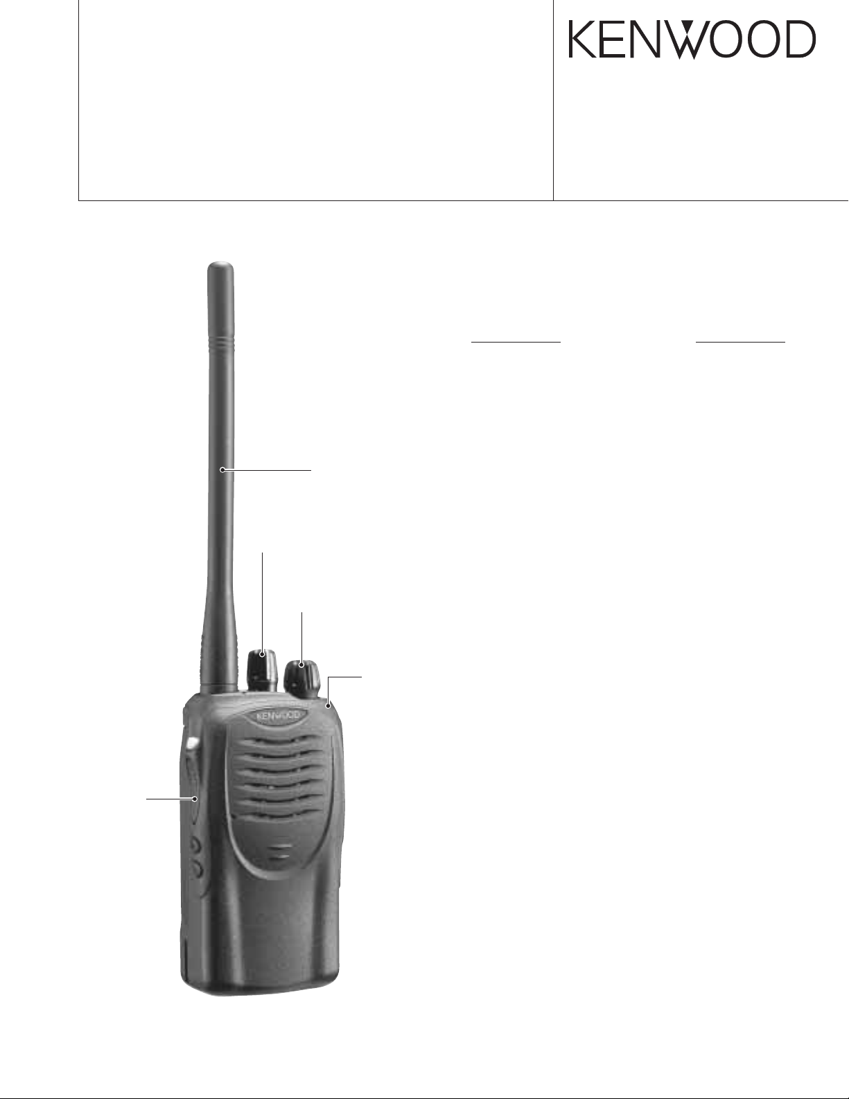
Antenna
(KRA-26: Option)
Knob (CH-SELECTOR)
(K29-9280-13)
Knob (VOLUME)
(K29-9278-13)
Cabinet assy
(A02-3826-33)
© 2003-8 PRINTED IN JAPAN
B51-8652-00 (S) 1214
CONTENTS
GENERAL .............................................................2
SYSTEM SET-UP .................................................2
OPERATING FEATURES ..................................... 3
REALIGNMENT....................................................4
DISASSEMBLY FOR REPAIR .............................. 5
CIRCUIT DESCRIPTION ....................................... 7
INSTALLATION..................................................11
TERMINAL FUNCTION......................................12
SEMICONDUCTOR DATA ................................. 13
COMPONENTS DESCRIPTION .........................14
PARTS LIST........................................................15
EXPLODED VIEW...............................................23
PACKING ............................................................ 24
ADJUSTMENT ................................................... 25
PC BOARD
TX-RX UNIT (X57-672X-XX) ........................30
SCHEMATIC DIAGRAM.....................................34
BLOCK DIAGRAM..............................................38
LEVEL DIAGRAM...............................................40
KSC-30................................................................41
SPECIFICATIONS............................BACK COVER
Knob (PTT)
(K29-9279-03)
Does not come with antenna.
Antenna is available as an option.
Page 2
TK-2160
GENERAL / SYSTEM SET-UP
INTRODUCTION
SCOPE OF THIS MANUAL
This manual is intended for use by experienced technicians
familiar with similar types of commercial grade communications
equipment. It contains all required service information for the
equipment and is current as of the publication date. Changes
which may occur after publication are covered by either Service
Bulletins or Manual Revisions. These are issued as required.
ORDERING REPLACEMENT PARTS
When ordering replacement parts or equipment information,
the full part identification number should be included. This
applies to all parts, components, kits, or chassis. If the part
number is not known, include the chassis or kit number of
which it is a part, and a sufficient description of the required
component for proper identification.
Unit
Model
& destination
TK-2160
TX-RX Unit Frequency range Remarks
K,M X57-6720-10 136~174MHz
IF1 : 49.95MHz
LOC : 50.4MHz
PERSONAL SAFETY
The following precautions are recommended for personal
safety:
●
DO NOT transmit until all RF connectors are verified secure
and any open connectors are properly terminated.
●
SHUT OFF and DO NOT operate this equipment near
electrical blasting caps or in an explosive atmosphere.
●
This equipment should be serviced by a qualified technician
only.
SERVICE
This radio is designed for easy servicing. Refer to the
schematic diagrams, printed circuit board views, and alignment
procedures contained within.
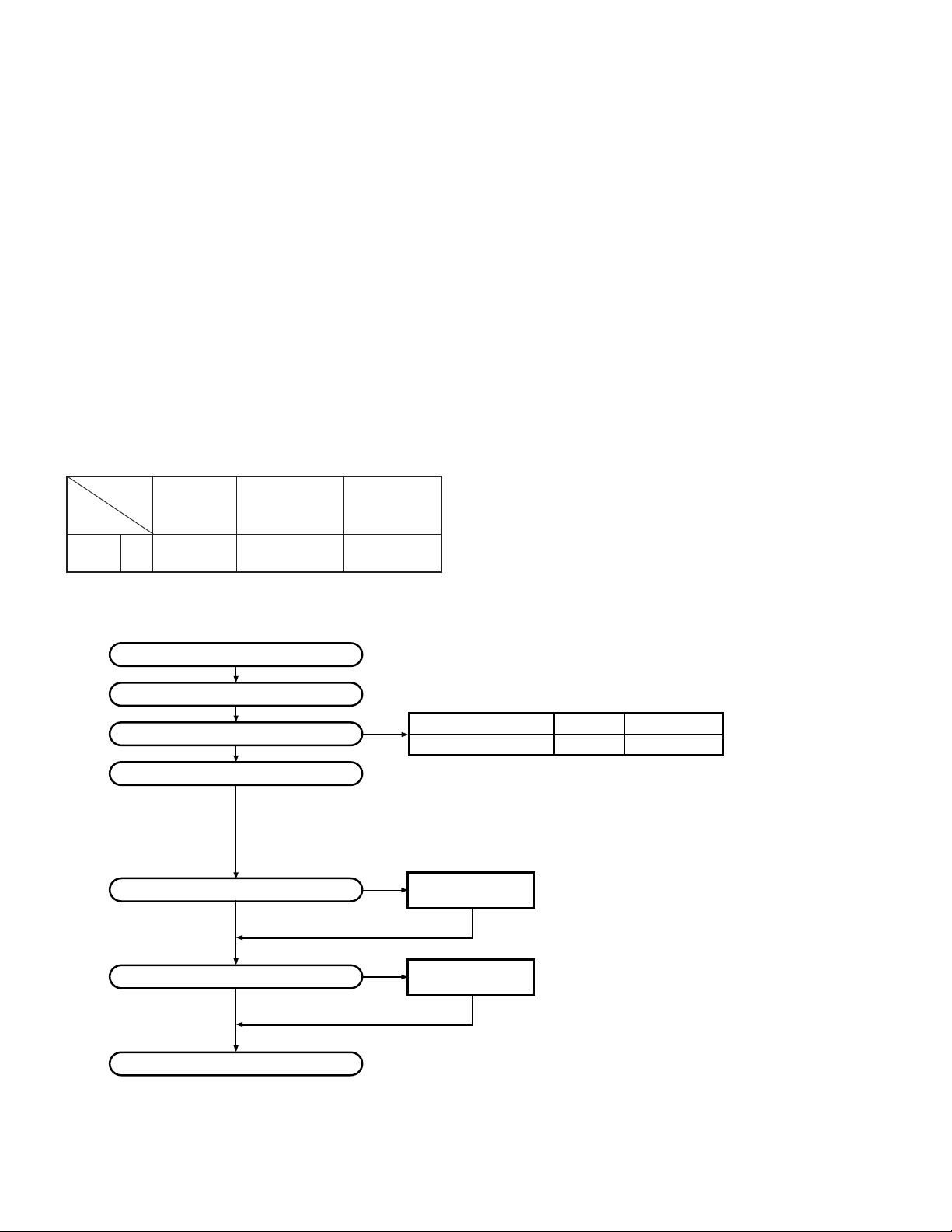
SYSTEM SET-UP
Merchandise received
License and frequency allocated by FCC
Choose the type of transceiver
Transceiver programming
Are you using the optional antenna?
Are you using the speaker microphone?
NO
NO
Delivery
Frequency range (MHz) RF power Type
TX/RX 136~174
A personal computer (IBM PC or compatible), programming
interface (KPG-22), and programming software (KPG-82D)
are required for programming.
(The frequency, TX power HI/LOW, and signalling data are programmed
for the transceiver.)
YES
YES
KRA-22 or KRA-26
Optional antenna
KMC-17 or KMC-21
Speaker microphone
(Option)
5.0W
TK-2160 (K,M)
2
Page 3
OPERATING FEATURES
4
1 2 3
5
8
6
7
TK-2160
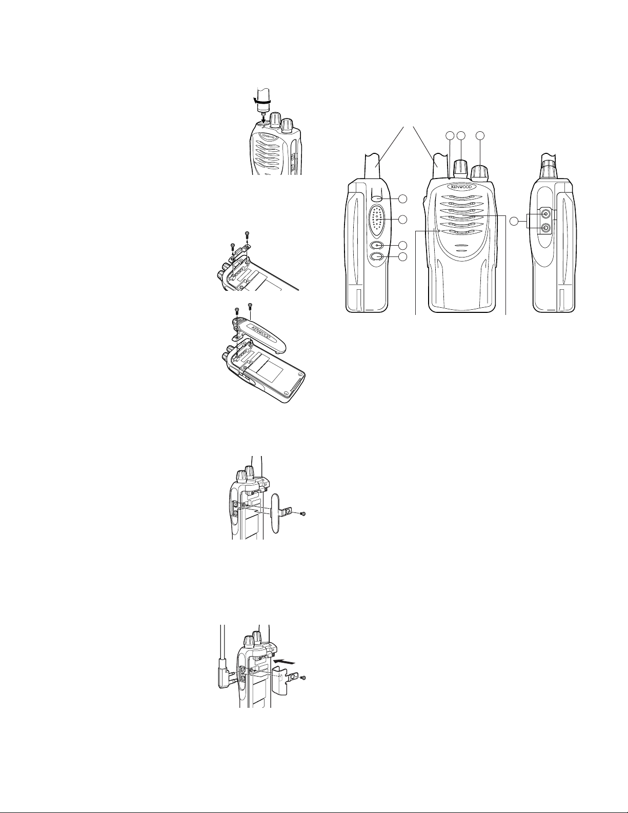
1. Operation Features
Installing the (Optional) Antenna
Screw the antenna into the connector on
the top of the transceiver by holding the
antenna at its base and turning it clockwise
until secure.
Installing the Belt Clip
Note: When first installing the belt clip, you must remove the
battery pack from the rear of the transceiver.
1 Remove the two screws from the
rear of the transceiver, then remove
the small, plastic black covering that
was held in place.
2 Insert the belt clip mount into the
space on the rear of the transceiver.
3 Using the 2 screws, affix the belt
clip in place.
Note: Do not dispose of the plastic
black covering! If you remove
the belt clip, replace the covering
into the space on the rear of the
transceiver. Either this covering
or the belt clip must be in place,
otherwise the battery pack may
not remain installed properly.
Installing the Cover over the
Speaker/ Microphone Jacks
Note: When installing the speaker/
microphone jack cover, you must
remove the battery pack from the
rear of the transceiver.
If you are not using a speaker/
microphone, install the cover over the
speaker/ microphone jacks using the
supplied screw.
Note: To lift the cover after it has been installed, use a piece
of hardened plastic or metal, such as a small screwdriver.
Lift the cover by its tab, beside the screwhole, taking
care not to damage the cover.
Installing the (Optional) Speaker/ Microphone
Note: When installing the optional
1 Insert the speaker/ microphone
2 Attach the locking bracket using the supplied screw.
Note: To lift the locking bracket after it has been installed,
speaker/ microphone and its
locking bracket, you must
remove the battery pack from
the rear of the transceiver.
plugs into the speaker/ microphone
jacks.
use a piece of hardened plastic or metal, such as a small
screwdriver. Lift the bracket by its tab, beside the
screwhole, taking care not to damage the bracket.
GETTING ACQUAINTED
Antenna
Microphone Speaker
The transceiver is shown with the optional KNB-24L battery
pack.
qq
q LED indicator
qq
Lights red while transmitting. Lights green while receiving.
Flashes orange while receiving a 2-Tone, DTMF, or
FleetSync signal that matches the one set up in your
transceiver. If programmed by your dealer, flashes red when
the battery power is low while transmitting.
w Channel Switch
Rotate to select a channel from 1 to 16.
e Power switch/ Volume control
Turn clockwise to switch ON the transceiver. Rotate to
adjust the volume. To switch OFF the transceiver, turn
counterclockwise fully.
r AUX key
This is a PF (Programmable Function) key. Press it to activate
its auxiliary function (page 4). The default setting for this
key is None.
t PTT (Push-to-Talk) switch
Press this switch, then speak into the microphone to call a
station.
y Side 1 key
This is a PF (Programmable Function) key. Press it to activate
its auxiliary function (page 4). The default setting for this
key is None.
u Side 2 key
This is a PF (Programmable Function) key. Press it to activate
its auxiliary function (page 4). The default setting for this
key is Squelch Off Momentary. Press each key to activate
its auxiliary function.
i SP/MIC jacks
Connect an optional speaker/ microphone here.
3
Page 4
TK-2160
OPERATING FEATURES /
Programmable Auxiliary Functions
The AUX, Side 1, and Side 2 keys can be programmed
with the auxiliary functions listed below:
• 2-Tone Encode
• Emergency
•Monitor Momentary
• Monitor Toggle
• None
• RF Power Low
•Scan
• Scan Temporary Delete
• Scrambler
• Squelch Off Momentary
• Squelch Off Toggle
∗1
This function can be programmed only on the AUX key.
REALIGNMENT
1. Modes
User mode
User mode For normal use.
PC mode Used for communication between the
Data programming Used to read and write frequency data
mode
PC test mode Used to check the radio using the PC.
2. How to Enter Each Mode
User mode Power ON
PC mode Received commands from PC
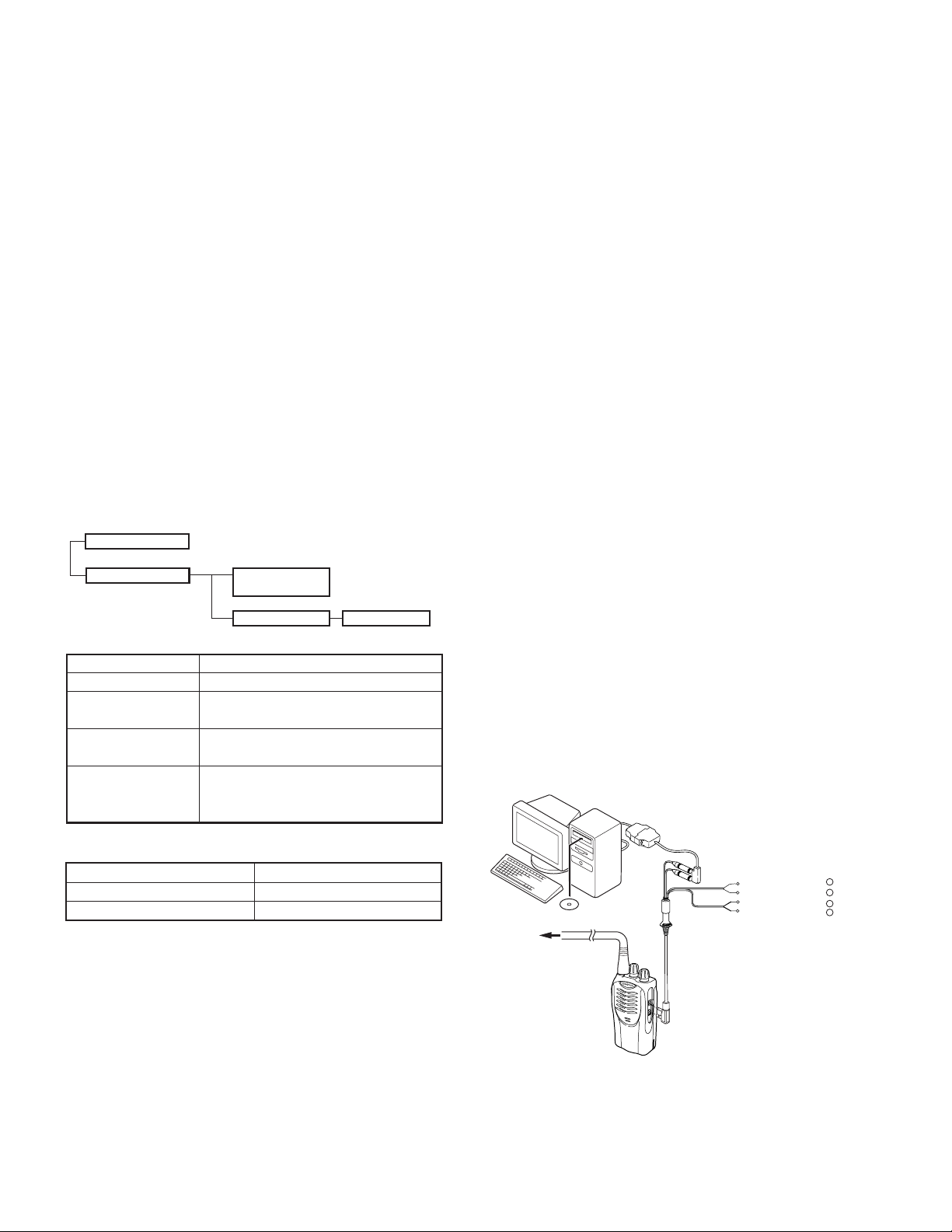
3.PC Mode
3-1. Preface
The TK-2160 transceiver is programmed using a personal
computer, a programming interface (KPG-22) and programming
software (KPG-82D).
The programming software can be used with an IBM PC
or compatible. Figure 1 shows the setup of an IBM PC for
programming.
∗1
PC mode
Mode Function
Mode Operation
Data programming
mode
PC test mode
radio and PC (IBM compatible).
and other features to and from the radio.
This feature is included in the KPG82D.
PC tuning mode
REALIGNMENT
3-2. Connection procedure
1. Connect the TK-2160 to the personal computer with the
interface cable.
2. When the POWER is switched on, user mode can be
entered immediately. When the PC sends a command,
the radio enters PC mode.
When data is transmitting from the transceiver, the red
LED lights.
When data is received by the transceiver, the green LED
lights.
Notes:
• The data stored in the personal computer must match the
model type when it is written into the EEPROM.
• Change the TK-2160 to PC mode, then attach the interface
cable.
3-3. KPG-22 description
(PC programming interface cable: Option)
The KPG-22 is required to interface the TK-2160 with the
computer. It has a circuit in its D-subconnector (25-pin) case
that converts the RS-232C logic level to the TTL level.
The KPG-22 connects the SP/MIC connector of the TK-2160
to the computer’s RS-232C serial port.
3-4. Programming software description
KPG-82D is the programming software for TK-2160
supplied on a CD-ROM. This software runs under Windows
98, ME, Windows 2000 or XP on an IBM-PC or compatible
machine.
The data can be input to or read from TK-2160 and edited
on the screen. The programmed or edited data can be printed
out. It is also possible to tune the transceiver.
IBM-PC
KPG-22
Gray +
Gray/Black –
1.5D-XV Lead wire +
1.5D-XV Shield wire –
RF Power meter
or SSG
KPG-82D
Fig. 1
Tuning cable
(E30-3216-05)
SP
}
MIC
}
4
Page 5
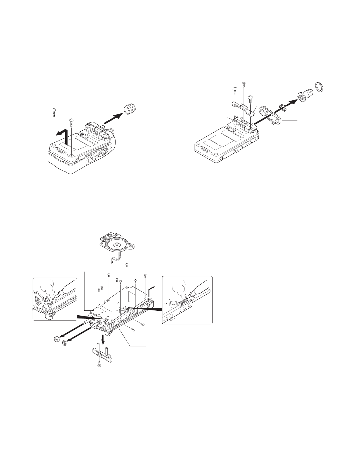
DISASSEMBLY FOR REPAIR
TK-2160
1. Separating the case assembly from the chassis.
1. Remove the volume knob z.
2. Remove the two screws
3. Lift the chassis
Note: After separating the case assembly from the chassis,
remove the channel knob.
and remove it from the case assembly.
c,
x
x
.
z
x
c
Channel knob
2. Separating the chassis from the TX/RX unit.
1. Remove the two screws v fixing the TX/RX unit B/2.
2. Remove the twelve screws
the TX/RX unit A/2.
3. Remove the solder from the antenna terminal using a
soldering iron
, then lift the unit off.
m
and two screws n fixing
b
3. How to remove the battery terminal block.
1. Remove the two screws /, then pull out the back cover Ω.
2. Remove the screw
≈.
≈
/
/
Ω
,
Packing
TX/RX UNIT A/2
m
b
b
b
b
b
b
b
n
v
v
TX/RX UNIT B/2
,
≈
Note: To remove the TX/RX unit B/2, remove the solder using
a soldering iron
Note: The two screws
battery terminal block
.
.
of TX/RX unit A/2 are fixing the
n
.
,
.
5
Page 6
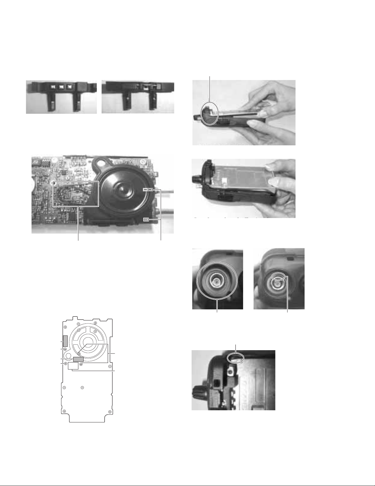
TK-2160
DISASSEMBLY FOR REPAIR
Assembling
•Installation of battery terminal block and
packing
Install them so that no distortion or deformation occurs.
•Installation of speakers and cushion, and wire
styling of speakers
•Installation of chassis and cabinet assy
Do not press this area, top
packing easily deform.
First, mount the set to the cabinet assy.
Second, press down the Chassis to the
cabinet assy as shown in the diagram.
Wire Styling
Install the speakers so that they do not protrude from the
cushion. Perform the wire styling of speakers as shown in a
photograph.
Install the cushion
according to the
guide.
• Attaching the cushion
Attach the cushion as shown in Fig. 1.
G13-2017-04
C
G13-2020-04
A
B
Fig. 1
Note: Cushion must not cover the screws A,B and C.
Take screw B and
MIC edge as reference
line when sticking.
G13-2018-04
Stick between screw
A and B.
Good Condition NG Condition
After mount, packing
should be in this
condition.
Packing protruded out.
Note:
• Take care that the packing does not protrude from the
chassis or case.
• Replace the protruded or deformed packing with a new one.
Packing deform.
6
Page 7
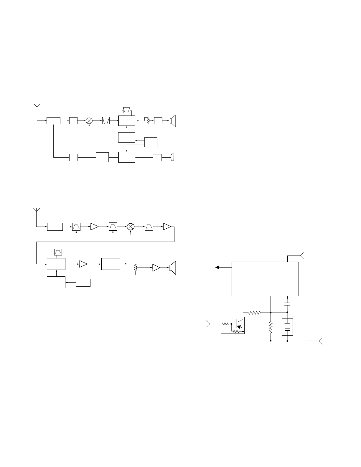
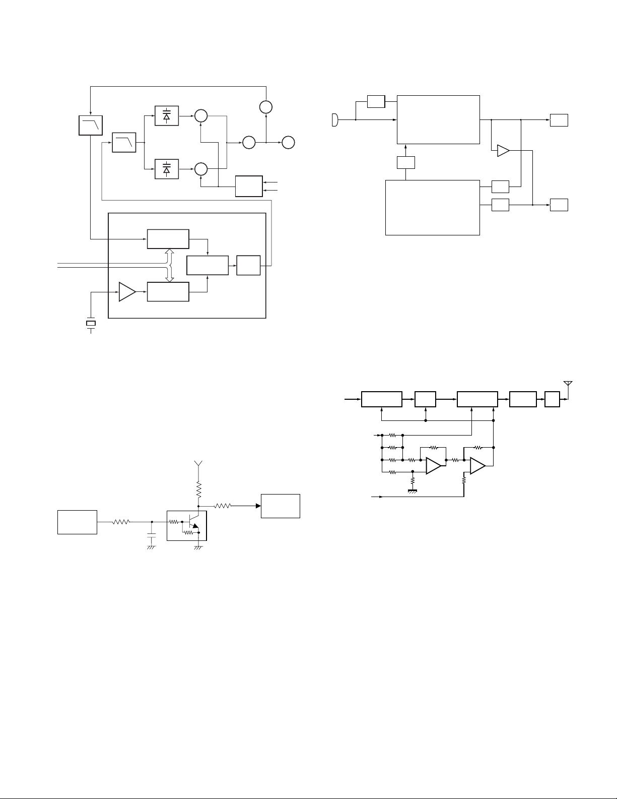
CIRCUIT DESCRIPTION
Q401
H : Wide
L : Narrow
C409
W/N
R408
R409
CD401
IFO
QUAD
IC401
FM IF SYSTEM
5R
AFOUT
Q402
TK-2160
1. Frequency Configuration
The receiver utilizes double conversion. The first IF is 49.95
MHz and the second IF is 450 kHz. The first local oscillator
signal is supplied from the PLL circuit.
The PLL circuit in the transmitter generates the necessary
frequencies. Fig. 1 shows the frequencies.
TX/RX: 136 ~ 174MHz (K,M)
ANT
ANT SW
TX: 136 ~ 174MHz (K,M)
RF
AMP
TX
AMP
MCF
49.95MHz
RX: 185.95 ~ 233.95MHz
(K,M)
RF
AMP
IF SYSTEM
50.4MHz
X3 multiply
CF
450kHz
PLL
VCO
TCXO
AMP
MIC
AMP
AF
16.8MHz
Fig. 1 Frequency configuration
2. Receiver
The frequency configuration of the receiver is shown in Fig. 2.
ANT
ANT SW
IC401
IF,MIX,DET
CF401
BPF
TUNE
IC602
AF Amp
RF AMP
Q404
IC601
AQUA
BPF
TUNE
MIXER
Q403
1st Local
AF VOL
MCF
XF401
IC605
AF PA
IF AMP
Q402
SP
MIC
SP
3) IF Amplifier Circuit
The first IF signal is passed through a four-pole monolithic
crystal filter (XF401) to remove the adjacent channel signal.
The filtered first IF signal is amplified by the first IF amplifier
(Q402) and then applied to the lF system IC (IC401). The
IF system IC provides a second mixer, second local
oscillator, limiting amplifier, quadrature detector and RSSI
(Received Signal Strength Indicator). The second mixer
mixes the first IF signal with the 50.4MHz of the second
local oscillator output (TCXO X1) and produces the second
IF signal of 450kHz.
The second IF signal is passed through the ceramic filter
(CF401) to remove the adjacent channel signal. The filtered
second IF signal is amplified by the limiting amplifier and
demodulated by the quadrature detector with the ceramic
discriminator (CD401). The demodulated signal is routed
to the audio circuit.
4) Wide/Narrow Switching Circuit
Narrow and Wide settings can be made for each channel
by switching the demodulation level.
The WIDE (high level) and NARROW (low level) data is
output from IC805, pin 54.
When a WIDE (high level) data is received, Q401 turn off.
When a NARROW (low level) data is received, Q401 turn on.
Q401 turns on/off with the Wide/Narrow data and the
IC401 detector output level is switched to maintain a
constant output level during wide or narrow signals.
Q4
X3 multiply
2nd Local
X1
TCXO
16.8MHz
Fig. 2 Receiver section
1) Front End (RF AMP)
The signal coming from the antenna passes through the
transmit/receive switching diode circuit, (D204,D206,D208
and D212) passes through a BPF (L411 and L412), and is
amplified by the RF amplifier (Q404).
The resulting signal passes through a BPF (L407 and L409)
and goes to the mixer. These BPFs are adjusted by variable
capacitors (D402,D403,D404 and D405). The input voltage
to the variable capacitor is regulated by voltage output from
the microprocessor (IC805).
2) First Mixer
The signal from the front end is mixed with the first local
oscillator signal generated in the PLL circuit by Q403 to
produce a first IF frequency of 49.95 MHz.
The resulting signal passes through the XF401 MCF to cut
the adjacent spurious and provide the opitimun
characteristics, such as adjacent frequency selectivity.
Fig. 3 Wide/Narrow switching circuit
5) Audio Amplifier Circuit
The demodulated signal from IC401 is amplified by IC602,
and goes to AF amplifier through IC601.
The signal then goes through an AF volume control
(VR801), and is routed to an audio power amplifier (IC605)
where it is amplified and output to the speaker.
7
Page 8
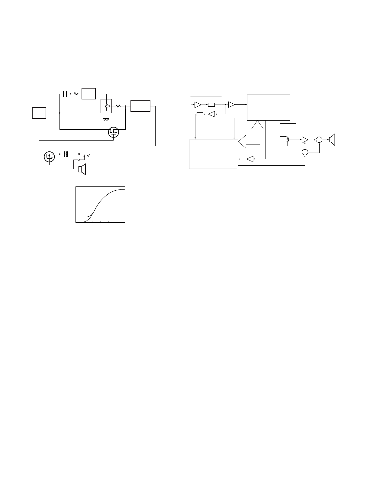
TK-2160
RECEIVE SIGNALING
CIRCUIT DESCRIPTION
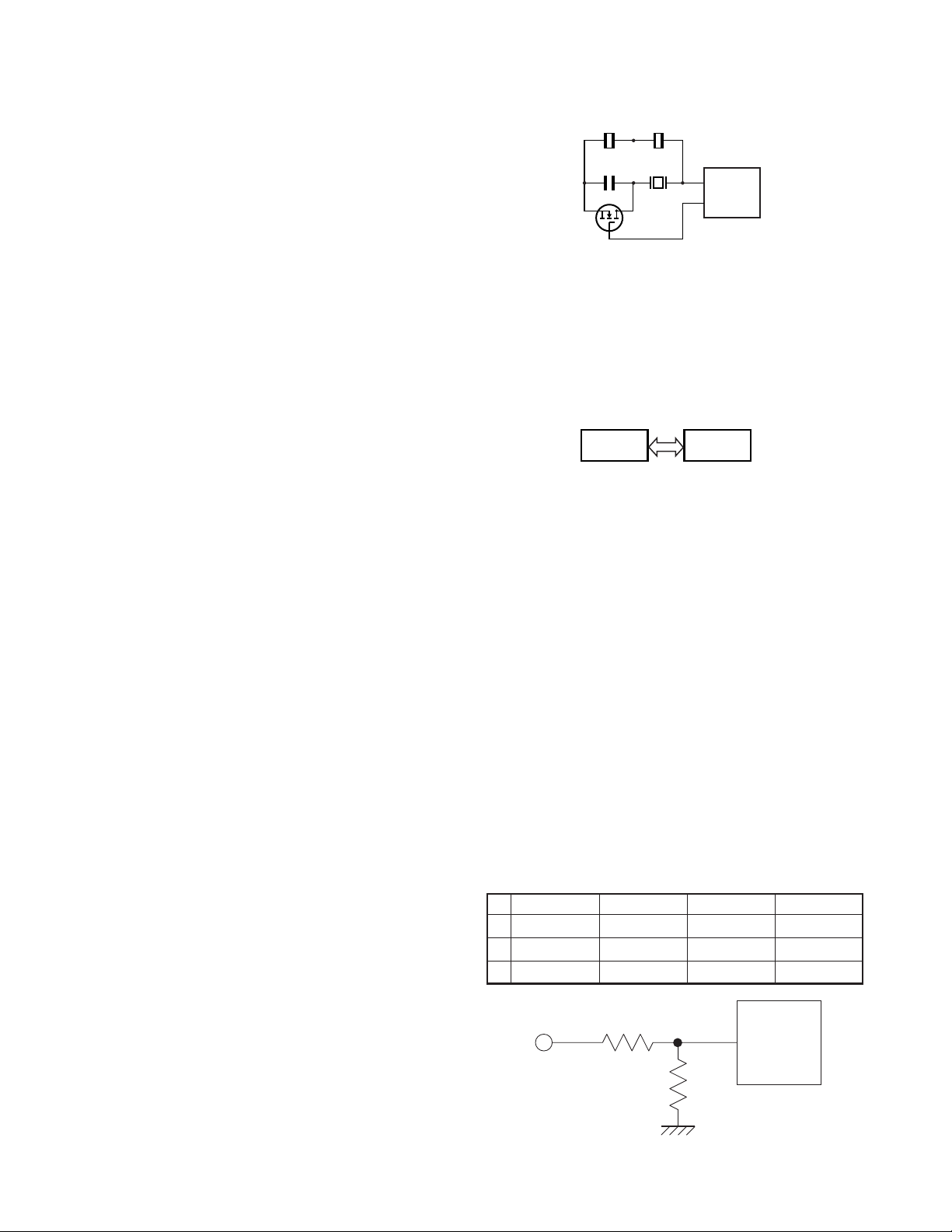
6) Tone Volume Fixed Circuit
This function generates a TONE signal sound even if the
AF volume of the transceiver is the minimum.
A TONE signal is sent through Q602 to the AF amplifier
when, in the FPU, “TONE Volume Fixed” is set to ON.
IC805
CPU
BEEP
BEEPSW
IC601
AQUA
TONE VOL FIXED
+
SP
[VOL Position vs Output Level]
500
ON
25
Output Level (mV)
Min
VOL
Q602
SP-J
OFF
Center Max
IC605
TA7368F
Hi: ON
LOW: OFF
Fig. 4 Tone volume fixed circuit
7) Squelch
Part of the AF signal from the IC enters the FM IC (IC401)
again, and the noise component is amplified and rectified
by a filter and an amplifier to produce a DC voltage
corresponding to the noise level.
The DC signal from the FM IC goes to the analog port of
the microprocessor (IC805). IC805 determines whether
to output sounds from the speaker by checking whether
the input voltage is higher or lower than the preset value.
To output sounds from the speaker, IC805 sends a high
signal to the SP MUTE line and turns IC605 on through
Q603,Q604,Q607 and Q608. (See Fig. 5)
8) Receive Signalling
(1) QT/DQT
The output signal from IF IC(IC401) enters the
microprocessor(IC805) through IC601. IC805 determines
whether the QT or DQT matches the preset value, and
controls the SP MUTE and the speaker output sounds
according to the squelch results.
(2) 2-TONE
Part of the received AF signal output from the AF amplifier
IC602, and then passes through an audio processor
(IC601), goes to the other AF amplifier IC603, is compared,
and then goes to IC805. IC805 checks whether 2-TONE
data is necessary. If it matches, IC805 carries out a
specified operation, such as turning the speaker on. (See
Fig. 5)
(3) MSK (Fleet Sync)
Fleet Sync utilizes 1200bps and 2400bps MSK signal is
output from pin 6 of IC601. And is routed to the VCO.
When encoding MSK, the microphone input signal is muted.
RECEIVE SIGNALING
FM IF IC401
IF Amp
AN SQL
CPU
IC805
IC602
IF Amp
LSDI
HSDI
SP MUTE
SIGNAL
DTMF
QT/DQT
CLK,DATA,
STD,LOADN
IC603
BPF & COMPALATER
2-TONE
IC601
AQUA
IC605
AF PA
Q603,604,607
SW
Fig. 5 AF amplifier and squelch
(4) DTMF
The DTMF input signal from the IF IC (IC401) is amplified
by IC602 and goes to IC601. The decoded information is
then processed by the CPU.
3. PLL Frequency Synthesizer
The PLL circuit generates the first local oscillator signal for
reception and the RF signal for transmission.
1) PLL
The frequency step of the PLL circuit is K:2.5,5,6.25 or
7.5kHz, M:6 or 6.25kHz.
A 16.8MHz reference oscillator signal is divided at IC1 by a
fixed counter to produce an oscillator (VCO) output signal
which is buffer amplified by Q9 then divided in IC1 by a
dual-module programmable counter. The divided signal is
compared in phase with the 5 or 6.25kHz reference signal
from the phase comparator in IC1. The output signal from
the phase comparator is filtered through a low-pass filter
and passed to the VCO to control the oscillator frequency.
(See Fig. 6)
2) VCO
The operating frequency is generated by Q6 in transmit
mode and Q5 in receive mode. The oscillator frequency is
controlled by applying the VCO control voltage, obtained
from the phase comparator, to the varactor diodes
(D3,D5,D7 and D8 in transmit mode and D4,D6,D9 and D10
in receive mode). The RX pin is set high in receive mode
causing Q8 and Q12 to turn Q6 off and Q5 on.
The TX pin is set high in transmit mode. The outputs from
Q5 and Q6 are amplified by Q9 and sent to the RF amplifiers.
Q608
SW
SP
8
Page 9
CIRCUIT DESCRIPTION
T
IC601
IC805
LPF
DTMF/2 TONE
LSDTCXO
LSDVCO
CPU
AGC
VCO
MIC
X1
TCXO
LPF
IC606
BUFFER
LPF
AQUA
TK-2160
Q6
TX VCO
Q5
RX VCO
5kHz/6.25kHz
PHASE
COMPARATOR
5kHz/6.25kHz
BUFF AMP
CHARGE
PLL DATA
X1
16.8MHz
LPF
D3, 5, 7, 8
LPF
D4, 6, 9, 10
PLL IC IC1
1N
REF OSC
1M
Fig. 6 PLL circuit
3) Unlock Detector
If a pulse signal appears at the LD pin of IC1, an unlock
condition occurs, and the DC voltage obtained from C19,R6
and Q1 causes the voltage applied to the microprocessor
to go high. When the microprocessor detects this condition,
the transmitter is disabled, ignoring the push-to-talk switch
input signal. (See Fig. 7)
5C
IC1
PLL IC
R6
Q1
R16
LD
C19
R7
Fig. 7 Unlock detector circuit
4. Transmitter System
1) Microphone Amplifier
The signal from the microphone passes through the IC601.
When encoding DTMF, it is turned OFF for muting the
microphone input signal by IC601.
The signal passes through the Audio processor (IC601) for
the maximum deviation adjustment, and goes to the VCXO
modulation input.
Q9
Q8, 12
T/R SW
PUMP
IC805
UL
CPU
Q7
DOUBLER
Q11
RF AMP
RX
TX
Fig. 8 Microphone amplifier
2) Drive and Final Amplifier
The signal from the T/R switch (D201 is on) is amplified by
the drive amplifier (Q207) to 50mW.
The output of the drive amplifier is amplified by the RF power
amplifier (Q211) to 5.0W (1W when the power is low). The
RF power amplifier consists of two MOS FET stages. The
output of the RF power amplifier is then passed through
the harmonic filter (LPF) and antenna switch (D204 and
D206) and applied to the antenna terminal.
D204
From
T/R SW
(D201)
PCTV
(IC805)
Q206
Pre-DRIVE
AMP
+B
VG
R264
R265
R270
Q207 Q211
DRIVE
AMP
IC201
(1/2)
RF
POWER AMP
VDD
IC201
(2/2)
D206
ANT
SW
VGVG
Fig. 9 Drive and final amplifier and APC circuit
3) APC Circuit
The APC circuit always monitors the current flowing through
the RF power amplifier (Q211) and keeps a constant current.
The voltage drop at R264, R265 and R270 is caused by the
current flowing through the RF power amplifier and this
voltage is applied to the differential amplifier IC201(1/2).
IC201(2/2) compares the output voltage of IC201(1/2) with
the reference voltage from IC805. The output of IC201(2/2)
controls the VG of the RF power amplifier, drive amplifier
and pre-drive amplifier to make both voltages the same.
The change of power high/low is carried out by the change
of the reference voltage.
4) Encode Signalling
(1) QT/DQT
QT,DQT data of the LSDTCXO Line is output from pin 22 of
the CPU. The signal passes through a low-pass CR filter
and goes to the TCXO(X1).
The QT,DQT data of the LSDVCO Line is output from pin
AN
LPF
9
Page 10
TK-2160
IC805
CPU
IC804
EEPROM
20 of the CPU. The signal passes through a low pass CR
filter, mixes with the audio signal, and goes to the VCO
modulation input. TX deviation is adjusted by the CPU.
(2) DTMF/2 TONE
High-speed data is output from pin 2 of the CPU. The signal
passes through a low-pass CR filter, and provides a TX and
SP out tone, and is then applied to the audio processor
(IC601). The signal is mixed with the audio signal and goes
to the VCO.
TX deviation is adjusted by the CPU.
(3) MSK (Fleet Sync)
The MSK input signal from the IF IC is amplified by IC602
(1/2) and goes to pin 31 of IC 601. The signal is demodulated
by MSK demodulator in IC 601. The demodulated data goes
to the CPU for processing.
CIRCUIT DESCRIPTION
Q810
Hi: OFF
LOW: ON
Fig. 10 Frequency shift circuit
2) Memory Circuit
Memory circuit consists of the CPU (IC805) and an EEPROM
(IC804). An EEPROM has a capacity of 64k bits that contains
the transceiver control program for the CPU and data such
as transceiver channels and operating features.
X801C834
XOUT
IC805
BSHIFT
5. Power Supply
There are 3.5V power supply for PLL circuit and five 5V
power supplies for the microprocessor: 5M,5MS,5C,5R, and
5T. 5M is always output while the power is on. 5M is always
output, but turns off when the power is turned off to prevent
malfunction of the microprocessor.
5C is a common 5V and is output when SAVE is not set to
OFF.
5R is 5V for reception and output during reception.
5T is 5V for transmission and output during transmission.
6. Control Circuit
The control circuit consists of a microprocessor (IC805) and
its peripheral circuits. It controls the TX-RX unit. IC805 mainly
performs the following:
(1) Switching between transmission and reception by the
PTT signal input.
(2) Reading system, group, frequency, and program data
from the memory circuit.
(3) Sending frequency program data to the PLL.
(4) Controlling squelch on/off by the DC voltage from the
squelch circuit.
(5)Controlling the audio mute circuit by the decode data input.
(6) Transmitting tone and encode data.
1) Frequency Shift Circuit
The microprocessor (IC805) operates at a clock of
7.3728MHz. This oscillator has a circuit that shifts the
frequency by BEAT SHIFT SW (Q810).
A beat sound may be able to be evaded from generation if
“Beat Shift” is set to ON when it is generated in the internal
spurious transmission modulated sound of a transceiver.
Fig. 11 Memory circuit
3) Low Battery Warning
The battery voltage is checked using by the microprocessor.
The transceiver generates a warning tone when it falls below
the warning voltage shown in the table.
(1)The red LED blinks when the battery voltage falls below
the voltage (1) shown in the table during transmission.
(2)The red LED blinks when the battery voltage falls below
the voltage (2) shown in the table during transmission.
Note:
The transceiver checks the battery voltage during reception
even when, in the FPU, the Battery Warning status function
is set to “On TX” (default setting).
However, the LED does not blink during reception. During
transmission, the LED blinks to generate the warning tone
of a low battery voltage.
(3)The transceiver immediately stops transmission when
the battery voltage falls below the voltage (3) shown in
the table. A message tone beeps while the PTT switch
is released.
Battery Case Li-ion Battery Ni-Cd Battery Ni-MH Battery
(1) 6.2[V] 6.5[V] 6.2[V] 6.2[V]
(2) 7.6[V] 7.1[V] 6.8[V] 7.0[V]
(3) 5.9[V] 6.2[V] 5.9[V] 5.9[V]
SB
R833
R834
IC805
88
CPU
10
Fig. 12 Low battery warning
Page 11
CIRCUIT DESCRIPTION / INSTALLATION
R608
C608
C619
C1
C3
TK-2160
4) Battery Type Detection
The transceiver automatically detects the battery type,
measuring the resistance between the S-terminal and +
terminal on the battery pack and changes the supplied
voltage to the S-tarminal as below. The microprocessor then
detects the battery type.
Resistor value Battery type Input voltage of S-terminal
1.8MΩ Li-ion 0.3~1.3V
560kΩ Ni-Cd 1.3~2.6V
220kΩ Ni-MH 2.6~5.0V
OPEN Battery case 0~0.3V
7. Control System
Keys and channel selector circuit.
The signal from the keys and channel selector are directly
input to the microprocessor, as shown in fig. 13.
Channel selector
70
EN1
69
EN2
68
EN3
67
EN4
IC805
CPU
Fig. 13 Control system
PTT
AUXSW
SIDE 1
SIDE 2
34
PTT
SW
74
AUX SW
75
76
SW2
SW1
INSTALLATION
1. Optional Board
Remove the TX/RX unit from the radio before installing the
optional board in the radio.
The procedure for removing the TX/RX unit is described in
the DISASSEMBLY FOR REPAIR section in the Service
Manual.
Install the optional board on the back of the TX/RX unit.
For details on installation of the optional board, refer to
Installation Information supplied with the optional board.
When installing the optional board, also refer to the chart in
TERMINAL FUNCTION section (page 12) given in the Service
Manual.
Note: To install and use the Scrambler Board, remove “R601”
and “R647” from the front of the TX/RX unit.
R647 R601
R633
C607
R607
R609
C609
C645
C614
617
C618
606
R610
R1
R2
R3
R640
R613
R615
R696
R628
R643
R642
C648
C646
R641
R629
R636
C637
R631
C641
R634
R647
CP808
R835
CP803
75
R840
76
R839
C4
C642
R632
R601
C633
R626
R627
C631
C634
C632
C643
++
CP809
C627
R622
C628
C636
C625
R623
26
C640
IC601
32
19
R621
C621
C622
R624
C630
R625
C846
CP810
R618
R695
C635
1725
16
10
+
L804
C610
C613
R616
L806
C847
+
VCC
CP812
51
R855
50
CP813
R856
CE
TX-RX UNIT (X57-6720-10)
Component side view
11
Page 12
TK-2160
TERMINAL FUNCTION
■ CN801
Pin
Designation
No.
1 GND GND Vss
2SB Switched B Output Voltage/7mA load DC (Battery terminal) ±0.5V
3A3 AUX3 Load >100kΩ (Low) Vss ~ 0.4V (High) Vdd-0.8V ~ Vdd
4 TXAFI Transmit AF input Input sensitivity/Impedance (1kHz std. dev.) 280±50mVrms @22kΩ Load
5A2 AUX2 Load >100kΩ (Low) Vss ~ 0.4V (High) Vdd-0.8V ~ Vdd
6A6 AUX6 Load >100kΩ (Low) Vss ~ 0.4V (High) Vdd-0.8V ~ Vdd
7A1 AUX1 Load >100kΩ (Low) Vss ~ 0.4V (High) Vdd-0.8V ~ Vdd
8A5 AUX5 Load >100kΩ (Low) Vss ~ 0.4V (High) Vdd-0.8V ~ Vdd
9A4 AUX4 Load >100kΩ (Low) Vss ~ 0.4V (High) Vdd-0.8V ~ Vdd
10 NC Non connection Non connection
11 5C DC 5V Output Voltage/10mA load 5.0±0.5V
12 DEO Discriminator signal output Output voltage/Impedance (1kHz std. mod.) 280±50mVrms @2.2kΩ Load
13 TXAFI Transmit AF input Input sensitivity/Impedance (1kHz std. dev.) 280±50mVrms @22kΩ Load
14 DEO Discriminator signal output Output voltage/Impedance (1kHz std. mod.) 280±50mVrms @2.2kΩ Load
15 NC Non connection Non connection
16 ALT Sidetone input
17 NC Non connection Non connection
18 NC Non connection Non connection
19 NC Non connection Non connection
20 GND GND Vss
Function Condition Value
Input sensitivity/Impedance
(1kHz rated AF power/Vol. MAX)
7 ±3mVrms @22kΩ Load
■ Solder point connection
Designation
MIC_I Mic input Input sensitivity/Impedance (1kHz std. dev.) 7±3mVrms @22kΩ Load
MIC_O Mic o utput
RA_I Receiver AF input Input sensitivity/Impedance (1kHz rated AF power/Vol. MAX) 75±20mVrms @22kΩ Load
RA_O Receiver AF output
A1 AUX1 Load >100kΩ (Low) Vss ~ 0.4V (High) Vdd-0.8V ~ Vdd
A2 AUX2 Load >100kΩ (Low) Vss ~ 0.4V (High) Vdd-0.8V ~ Vdd
A3 AUX3 Load >100kΩ (Low) Vss ~ 0.4V (High) Vdd-0.8V ~ Vdd
A4 AUX4 Load >100kΩ (Low) Vss ~ 0.4V (High) Vdd-0.8V ~ Vdd
A5 AUX5 Load >100kΩ (Low) Vss ~ 0.4V (High) Vdd-0.8V ~ Vdd
A6 AUX6 Load >100kΩ (Low) Vss ~ 0.4V (High) Vdd-0.8V ~ Vdd
SB Switched B Output Voltage/7mA load DC (Battery terminal) ±0.5V
GND GND Vss
5C DC 5V Output Voltage/10mA load 5.0±0.5V
TXAFI Transmit AF input Input sensitivity/Impedance (1kHz std. dev.) 280±50mVrms @22kΩ Load
DEO Discriminator signal output Output voltage/Impedance (1kHz std. mod.) 280±50mVrms @2.2kΩ Load
LSDFO Received sub-tone output Output voltage/Impedance (150Hz 15% mod.) 180±50mVrms @2.2kΩ Load
ALT Sidetone input Input sensitivity/Impedance (1kHz rated AF power/Vol. MAX) 7±3mVrms @22kΩ Load
Function Condition Value
Output voltage/Impedance (1kHz 15mVrms mic input) 2.6±1.0mVrms @2.2kΩ Load
Output voltage/Impedance (1kHz 100mVrms mic input) 90±20mVrms @100kΩ Load
Output voltage/Impedance (1kHz std. mod.) 150±50mVrms @2.2kΩ Load
Output voltage/Impedance (1kHz system mod.) 290±50mVrms @100kΩ Load
12
Page 13

SEMICONDUCTOR DATA
Microprocessor : M30622MCA7G7GP (TX-RX UNIT : IC805)
■ Pin function
Pin Port
No. Name
1 PCTV O APC/BPF control data output.
2 DTMF O DTMF, 2TONE.
3 HSDI I High speed data input (2TONE).
4 EEPDAT I/O EEPROM data input/output.
5 EEPCLK O EEPROM Clock
6 BYTE I GND.
7 CNVSS I GND.
8 AUX5 O Option Board 5
9 AUX6 O Option Board 6
10 RESET I CPU reset.
11 XOUT O CPU clock.
12 VSS - GND.
13 XIN I CPU clock.
14 VCC - +5V.
15 NC I NC
16 INT I Battery voltage monitor input Low battery : L
17 RDF/FD I Base Band IC Data input
TCLK/
18
DTRDI
19 NC - NC
20 LSDVCO O Low speed data output (VCO).
21 NC I NC
22
LSDTCXO
23 NC I NC
24 BEEP O Beep output.
25 OPTDET I Option detect input
26 NC - NC
27 NC - NC
28 NC - NC
29 AUX4 O Option board port 4
30 AUX2 I/O Option board port 2
31 NC - NC
32 NC - NC
33 TXD I/O Serial data.
34 PTT/RXD I PTT on : L/Serial data.
35 STD I Base Band IC Data input
36 BBDIR O Base Band IC Data output
37 BBCLK O Base Band IC clock output
38 BBDI/O I/O Base Band IC Data input/output
39 NC - NC
TDATA/
40
DTRCLK
41
DTRLOADN
42 AUX3 O Option board port 3
43 AUX1 O Option board port 1
44 NC - NC
45 NC - NC
46 DSW O APC voltage discharge Switch
47
BEEPSW
48 AFCOUT O AF amp power supply control
49 AFMUTE O RX audio mute
50 NC - NC
51 TX O TX VCO power supply switch TX:L
52 RX O RX VCO power supply switch RX:L
I/O Function
I Base Band IC Data input
O Low speed data output (TCXO).
O Base Band IC Data output
O Base Band IC Data output
O Beep switch.
Pin Port
No. Name
53 BSHIFT O Beet shift switch.
54 W/N O W/N switch Wide:H
55 NC - NC
56 APCSW O APC switch output.
57 SAVE O Battery save output.
58 5TC O 5T control output.
59 5RC O 5R control output.
60 VCC - +5V.
61 5MSC O 5M control output.
62 VSS - GND.
63 NC - NC
64 NC - NC
65 NC - NC
66 NC - NC
67 EN4 I CH selector input 4.
68 EN3 I CH selector input 3.
69 EN2 I CH selector input 2.
70 EN1 I CH selector input 1.
71 NC - NC
72 LEDTX O RED LED lights control output
73 LEDRX O GREEN LED lights control output
74 AUXSW I Key input (Emergency).
75 SIDE1 I Side key 1 input.
76 SIDE2 I Side key 2 input.
77 NC - NC
78 NC - NC
79 SIM1 I Destination select 1.
80 SIM2 I Destination select 2.
81 NC - NC
82 PLLUL I PLL unlock detect input. unlock : L
83 RFCLK O PLL clock output. Latch : L
84 RFDAT O PLL data output.
85 PS O PLL power save output.
86 PLLSTB O PLL strobe output.
87
BATTSEL
88 BATT I Battery voltage input.
89 VOX I VOX input.
90 RSSQL I Received signal strength indicator input.
91 ANSQL I Squelch level input.
92 LSDI I Low speed data input (QT/DQT).
93 THM I Thermistor input.
94 AVSS - GND.
95 NC - NC
96 VREF - +5V.
97 AVCC - +5V.
98 NC - NC
99 NC - NC
100 NC - NC
TK-2160
I/O Function
I Battery distinction input.
13
Page 14

TK-2160
TX-RX UNIT (X57-672X-XX)
Ref. No.
IC201 IC Comparator (APC)
IC401 IC FM IF system
IC601 IC Audio processor
IC602 IC AF AMP
IC603(1/2)
IC603(2/2)
IC604 IC VOX AMP
IC605 IC AF Power AMP
IC606 IC AF AMP
IC801 IC Voltage regulator / 5V
IC802 IC Voltage detector / Reset
IC803 IC Voltage detector / INT
IC804 IC EEPROM
IC805 IC Microprocessor
IC806 IC Flip Flop
Q206 FET Pre-drive AMP
Q207 FET TX Drive AMP
Q208 Transistor APC switch
Q209 FET APC switch
Q210 Transistor APC switch
Q211 FET TX Final AMP
Q212 FET APC switch
Q213 Transistor APC switch
Q400 FET W/N switch / TX
Q401 Transistor W/N switch / RX
Q402 Transistor IF AMP
Q403 FET Mixer
Q404 FET RF AMP
Q601 FET AF Mute
Q602 FET Beep switch
Q603 Transistor DC switch / SP Mute
Q604 Transistor DC switch
Q605 Transistor MIC AGC
Q606 Transistor MIC AGC
Q607 Transistor DC switch / SP Mute
Q608 FET SP Mute switch
Q801 Transistor 5T switch
Q802(1/2) FET 5TC switch
Q802(2/2) FET SAVE switch
Q803(1/2) Transistor AVR / 5C
Q803(2/2) Transistor AVR / 5T
14
Use/Function
IC1 IC PLL system
IC HSD AMP
IC HSD AMP
Q1 Transistor Level shift
Q2 Transistor Level shift
Q3 Transistor Level shift
Q4 Transistor Tripler
Q5 FET VCO / RX
Q6 FET VCO / TX
Q7 Transistor Doubler
Q8 FET DC switch / TX VCO
Q9 Transistor RF Buffer AMP
Q10 Transistor Ripple filter
Q11 Transistor RF AMP
Q12 FET DC switch / RX VCO
COMPONENTS DESCRIPTION
Operation/Condition
Ref. No.
Q804 Transistor 5C switch
Q805(1/2) Transistor LED switch / Green
Q805(2/2) Transistor LED switch / Red
Q806 Transistor AVR / PLLB
Q807 Transistor PLLB switch
Q808 Transistor 5MS switch
Q809 Transistor 5R switch
Q810 FET Beet shift switch
D201 Diode TX/RX RF switch
D203 Zener diode APC protect
D204 Diode ANT switch
D206 Diode ANT switch
D208 Diode ANT switch
D212 Diode ANT switch
D401 Diode TX/RX RF switch
D402
D403
D404
D405
D603 Diode Limitter
D604 Diode Detector
D605 Diode Detector
D606 Diode Detector
D801 Diode 5M protector
D802 LED LED / Red
D803 LED LED / Green
D805 Diode Reverse protection
Use/Function
D2 diode Shift switch
Variable
D3
capacitance diode
Variable
D4
capacitance diode
Variable
D5
capacitance diode
Variable
D6
capacitance diode
Variable
D7
capacitance diode
Variable
D8
capacitance diode
Variable
D9
capacitance diode
Variable
D10
capacitance diode
D11 Diode Shift switch
Variable
D12
capacitance diode
D13 Diode Current steering
D14 Diode Shift switch
Variable
capacitance diode
Variable
capacitance diode
Variable
capacitance diode
Variable
capacitance diode
Operation/Condition
Frequency control / TX VCO
Frequency control / RX VCO
Frequency control / TX VCO
Frequency control / RX VCO
Frequency control / TX VCO
Frequency control / TX VCO
Frequency control / RX VCO
Frequency control / RX VCO
Modulator
RF BPF tuning
RF BPF tuning
RF BPF tuning
RF BPF tuning
Page 15

PARTS LIST
TK-2160
CAPACITORS
1 = Type ... ceramic, electrolytic, etc.
2 = Shape ... round, square, ect.
3 = Temp. coefficient
Temperature coefficient
1st Word
Color*
ppm/
Tolerance (More than 10pF)
Code
(%)
Voltage rating
1st word
Black Red Orange Yellow Green Blue Violet
0 -80 -150 -220
C
0.25 0.5 2 5 10 20
2nd word
0
1
2
3
CC 45
1
1
2
LCPRSTU
DGJKMXZP
BCDEF
A
1.0
1.25
10
12.5
100
125
1000
1250
TH 1H J220
3
4
5
4 = Voltage rating
5 = Value
6 = Tolerance
2.0
1.6
20
16
200
160
2000
1600
6
-330 -470 -750
+ 40
+ 80
- 40
- 20
3.15
2.5
31.5
25
315
250
3150
2500
CC45
+ 100
-0
G
4.0
40
400
4000
Color*
2nd Word HG
ppm/
Example : CC45TH = -470
No code
More than 10µF -10 +50
Less than 4.7µF -10 +75
H
J
5.0
6.3
50
63
500
630
5000
6300
Capacitor value
010 = 1pF
100 = 10pF
101 = 100pF
102 = 1000pF = 0.001µF
103 = 0.01µF
30 60
K
V
8.0
-
80
35
800
-
8000
-
22
JKL
120 250 500
60ppm/
(Less than 10pF)
Gode
0.1 0.25 0.5 1 2
(pF)
0 = 22pF
Multiplier
2nd number
1st number
CDFGB
Chip capacitors
(EX) C C 7 3 F S L 1 H
(Chip)(CH,RH<UJ,SL)
(EX) C K 7 3 F F 1 H
(Chip)(B,F)
RESISTORS
Chip resistor (Carbon)
(EX) R K 7 3 E B 2 B
(Chip)(B,F)
Carbon resistor (Nomal type)
(EX) R D 1 4 B B
1 = Type
2 = Shape
3 = Dimension
4 = Temp. coefficient
2C
000
000
000
000
J
7654321
Z
7654321
J
7654321
J
7654321
5 = Rating wattage
6 = Value
7 = Tolerance
Refer to the table above.
1 = Type
2 = Shape
3 = Dimension
4 = Temp. coefficient
5 = Voltage rating
6 = Value
7 = Tolerance
Dimension (Chip capacitors)
Dimension code L W T
Empty
A
B
C
D
E
F
G
H
Dimension
Dimension (Chip resistor)
Dimension code L W T
E
F
G
H
Rating wattage
Code
1J
2A
2B
Wattage
1/16W
1/10W
Code
1/8W
2C
2E
2H
5.6
4.5
4.5
4.5
3.2
3.0
2.0
1.6
1.0
L
W
3.2
2.0
1.6
1.0
0.5
0.5
0.5
0.5
0.4
0.2
0.3
0.2
0.05
0.2
0.3
0.2
0.05
Wattage
1/6W
1/4W
1/2W
5.0
3.2
2.0
1.25
2.5
1.6
1.25
0.8
0.5
1.6
1.25
0.8
0.5
Code
0.5
0.4
0.3
0.2
0.3
0.2
0.2
0.2
0.05
T
0.2
0.2
0.2
0.05
Wattage
3A
3D
Less than 2.0
Less than 2.0
Less than 2.0
Less than 1.25
Less than 1.5
Less than 1.25
Less than 1.25
Less than 1.0
0.5
0.5
0.35
1W
2W
0.05
1.0
1.0
0.1
0.05
15
Page 16

TK-2160
New Parts. indicates safety critical components.
∗
Parts without Parts No. are not supplied.
Les articles non mentionnes dans le Parts No. ne sont pas fournis.
Teile ohne Parts No. werden nicht geliefert.
TK-2160 (Y50-578X-XX)
TX-RX UNIT (X57-672X-XX)
Ref. No.
11B∗ A02-3826-33 CABINET ASSY
22B∗ A10-4068-01 CHASSIS
33A∗ A82-0054-02 REAR PANEL
43AB01-0694-03 ESCUTCHEON
52D∗ B09-0676-03 CAP ACCESSORY
61C∗ B62-1716-00 INSTRUCTION MANUAL K
61C∗ B62-1747-00 INSTRUCTION MANUAL M
73B∗ B72-2153-04 MODEL NAME PLATE
83A∗ E04-0446-05 RF COAXIAL RECEPTACLE(SMA)
93B∗ E37-1085-05 FLAT CABLE
10 2A ∗ E37-1101-05 SPEAKER WIRE(RED)
11 2A ∗ E37-1102-05 SPESKER WIRE(BLACK)
12 3A ∗ E72-0416-13 BATT TERMINAL BLOCK
13 ∗ G10-1315-04 FIBROUS SHEET(CABINET)
14 2B G11-4090-04 SHEET(FINAL FET)
15 3B ∗ G11-4254-04 SHEET(PTT)
16 3A ∗ G11-4287-04 SHEET(TERMINAL BLOCK)
17 3A ∗ G11-4289-04 SHEET(CHASSIS)
18 2B ∗ G13-2001-04 CUSHION(CHASSIS)
19 2B ∗ G13-2014-04 CUSHION(CHASSIS BOTTOM)
20 2B ∗ G13-2017-04 CUSHION
21 2B ∗ G13-2018-04 CUSHION
22 3A ∗ G13-2019-04 CUSHION
23 2B ∗ G13-2020-04 CUSHION
24 3A ∗ G53-1579-02 PACKING
25 2B ∗ G53-1580-03 PACKING(CHASSIS)
26 1B ∗ G53-1581-22 PACKING(SPEAKER)
27 3B ∗ G53-1582-03 PACKING(BATT TERMINAL BLOCK)
28 3C ∗ H12-3150-02 PACKING FIXTURE
29 ∗ H25-2345-04 PROTECTION BAG
30 1D ∗ H52-1981-02 ITEM CARTON CASE
31 2A ∗ J19-5454-03 HOLDER
32 2D ∗ J21-8464-04 HARDWARE FIXTURE ACCESSORY
33 2C J29-0701-05 HOOK ACCESSORY
34 3A ∗ J30-1275-04 SPACER(CH KNOB)
35 3A ∗ J30-1281-04 SPACER(CH KNOB)
36 ∗ J30-1283-04 SPACER
37 1A ∗ K29-9278-13 KNOB(VOLUME)
38 1B ∗ K29-9279-03 KNOB(PTT)
39 3A ∗ K29-9280-13 KNOB(CH SELECTOR)
A3AN14-0583-04 CIRCULAR NUT(CH)
B3A∗ N14-0805-04 CIRCULAR NUT(VOLUME)
C3AN30-2604-46 PAN HEAD MACHINE SCREW
D3BN30-2612-46 PAN HEAD MACHINE SCREW
E 3A,3B N30-3006-45 PAN HEAD MACHINE SCREW
F2DN35-3004-45 BINDING HEAD MACHINE SCREW
G 3A,3B ∗ N78-2040-46 PAN HEAD TAPTITE SCREW
H 2A,2B N83-2005-46 PAN HEAD TAPTITE SCREW
40 2A ∗ R31-0650-05 VARIABLE RESISTOR
41 2A S60-0420-05 ROTARY SWITCH
Address
New
Parts No. Description
parts
TK-2160
PARTS LIST
L:
Scandinavia
Y:
PX (Far East, Hawaii)
Y:
AAFES (Europe)
Destination Destination
Ref. No.
42 1B T07-0369-05 SPEAKER
Address
TX-RX UNIT (X57-672X-XX) 0-10 : K, M
D802 B30-2156-05 LED(RED)
D803 B30-2157-05 LED(YELLOW)
C1 CK73GB1H822K CHIP C 8200PF K
C2 CK73GB1H102K CHIP C 1000PF K
C3 CK73GB1E123K CHIP C 0.012UF K
C4 CK73GB0J225K CHIP C 2.2UF K
C5 CK73GB1H102K CHIP C 1000PF K
C6 CK73GB1H103K CHIP C 0.010UF K
C7 CK73GB1H102K CHIP C 1000PF K
C8 CC73GCH1H100D CHIP C 10PF D
C9 CK73GB1H103K CHIP C 0.010UF K
C10 CC73GCH1H100D CHIP C 10PF D
C11-13 CC73GCH1H101J CHIP C 100PF J
C14 C92-0713-05 CHIP-TAN 10UF 6.3WV
C15 CK73GB1H102K CHIP C 1000PF K
C16 CC73GCH1H470J CHIP C 47PF J
C18,19 CK73GB1C104K CHIP C 0.10UF K
C22 CK73GB1C104K CHIP C 0.10UF K
C23 CK73GB0J225K CHIP C 2.2UF K
C24 C92-0713-05 CHIP-TAN 10UF 6.3WV
C25 CK73GB1H102K CHIP C 1000PF K
C27 CK73GB1H102K CHIP C 1000PF K
C28 CC73GCH1H560J CHIP C 56PF J
C30 CC73GCH1H220J CHIP C 22PF J
C31 CC73GCH1H560J CHIP C 56PF J
C32 C92-0002-05 CHIP-TAN 0.22UF 35WV
C33 CC73GCH1H470J CHIP C 47PF J
C34 CK73GB1H102K CHIP C 1000PF K
C35 CC73GCH1H680J CHIP C 68PF J
C36 C92-0560-05 CHIP-TAN 10UF 6.3WV
C37 CK73GB1H102K CHIP C 1000PF K
C38,39 C92-0504-05 CHIP-TAN 0.68UF 20WV
C40 CK73GB1H471K CHIP C 470PF K
C41 CK73GB1H103K CHIP C 0.010UF K
C42 CK73GB1H183K CHIP C 0.018UF K
C43 CK73GB1A105K CHIP C 1.0UF K
C44 CK73FB1A225K CHIP C 2.2UF K
C45 CC73GCH1H120J CHIP C 12PF J
C46 CC73GCH1H090B CHIP C 9.0PF B
C47 CC73GCH1H040B CHIP C 4.0PF B
C48 CK73HB1C103K CHIP C 0.010UF K
C49 CK73HB1H102K CHIP C 1000PF K
C50 CC73GCH1H120J CHIP C 12PF J
C52 CC73GCH1H050B CHIP C 5.0PF B
C53 CC73HCH1H560J CHIP C 56PF J
C54 CC73HCH1H220J CHIP C 22PF J
C55 CC73GCH1H050B CHIP C 5.0PF B
C56,57 CC73HCH1H270J CHIP C 27PF J
C58 CC73GCH1H150J CHIP C 15PF J
C59 CC73HCH1HR75C CHIP C 0.75PF C
C60 CC73GCH1H070B CHIP C 7.0PF B
C61 CC73HCH1H070B CHIP C 7.0PF B
K:
New
parts
USA
T:
England
X:
Australia
P:
Canada
E:
Europe
M:
Other Areas
Parts No. Description
16
Page 17

New
Ref. No.
C62 CK73GB1E103K CHIP C 0.010UF K
C63 CC73GCH1H220J CHIP C 22PF J
C64 CC73GCH1H4R5B CHIP C 4.5PF B
C65 CC73HCH1H120J CHIP C 12PF J
C66 CK73GB1H102K CHIP C 1000PF K
Address
Parts No. Description
parts
TK-2160
PARTS LIST
TX-RX UNIT (X57-672X-XX)
New
Destination Destination
Ref. No.
C344 CC73GCH1H820J CHIP C 82PF J
C349 CC73GCH1H030B CHIP C 3.0PF B
C351 CK73GB1H102K CHIP C 1000PF K
C352 CC73GCH1H270G CHIP C 27PF G
C353 CC73GCH1H270J CHIP C 27PF J
Address
Parts No. Description
parts
C67 CK73HB1C103K CHIP C 0.010UF K
C69 CK73GB1E103K CHIP C 0.010UF K
C70 C92-0714-05 CHIP-TAN 4.7UF 6.3WV
C71 CC73HCH1H0R5B CHIP C 0.5PF B
C72 CC73HCH1H040B CHIP C 4.0PF B
C73 CK73GB1H102K CHIP C 1000PF K
C74 CC73HCH1H0R5B CHIP C 0.5PF B
CC75,76 CK73HB1H102K CHIP C 1000PF K
C77 C92-0713-05 CHIP-TAN 10UF 6.3WV
C78 CK73HB1H102K CHIP C 1000PF K
C80 CC73HCH1H330J CHIP C 33PF J
C81 CC73HCH1H150J CHIP C 15PF J
C82-84 CK73HB1H102K CHIP C 1000PF K
C85 CC73HCH1H100D CHIP C 10PF D
C86 CC73GCH1H090D CHIP C 9.0PF D
C87 CC73GCH1H060B CHIP C 6.0PF B
CC201,202 CK73GB1H102K CHIP C 1000PF K
C203 CC73GCH1H470J CHIP C 47PF J
C212 CK73GB1H102K CHIP C 1000PF K
C241 CK73GB1H102K CHIP C 1000PF K
C242 CC73GCH1H390J CHIP C 39PF J
C243 CK73GB1C104K CHIP C 0.10UF K
C246 CK73GB1H102K CHIP C 1000PF K
C248 CK73GB1H102K CHIP C 1000PF K
C249 CC73GCH1H100D CHIP C 10PF D
C255 CK73GB1H102K CHIP C 1000PF K
C258 CK73GB1C104K CHIP C 0.10UF K
C265 CC73GCH1H220J CHIP C 22PF J
C273 CC73GCH1H101J CHIP C 100PF J
C277 CC73GCH1H270J CHIP C 27PF J
C355 CK73GB1H102K CHIP C 1000PF K
C356 CC73GCH1H060D CHIP C 6.0PF D
C358 CC73GCH1H100D CHIP C 10PF D
C359 CC73GCH1H240J CHIP C 24PF J
C360 CC73GCH1H120J CHIP C 12PF J
C362 CC73GCH1H110J CHIP C 11PF J
C363 CC73GCH1H070D CHIP C 7.0PF D
C365 CC73GCH1H330J CHIP C 33PF J
C368 CC73GCH1H030C CHIP C 3.0PF C
C400 CK73GB0J225K CHIP C 2.2UF K
C401 CK73GB1H182K CHIP C 1800PF K
CC402,403 CC73GCH1H271J CHIP C 270PF J
C405 CC73GCH1H390J CHIP C 39PF J
C406 C92-0713-05 CHIP-TAN 10UF 6.3WV
C407 CK73GB1H103K CHIP C 0.010UF K
C408 CK73GB1C104K CHIP C 0.10UF K
C409 CC73GCH1H680J CHIP C 68PF J
C410 CK73GB1H102K CHIP C 1000PF K
C411-413 CK73GB1C104K CHIP C 0.10UF K
C414 CC73GCH1H330J CHIP C 33PF J
C415 CK73GB1H102K CHIP C 1000PF K
CC416,417 CK73GB1H103K CHIP C 0.010UF K
C418 CK73GB1H102K CHIP C 1000PF K
C419 CC73GCH1H010B CHIP C 1.0PF B
C420 CK73GB1C104K CHIP C 0.10UF K
C421 CC73GCH1H080B CHIP C 8.0PF B
C422 CK73GB1H103K CHIP C 0.010UF K
C424 CK73GB1H103K CHIP C 0.010UF K
C425 CC73GCH1H150J CHIP C 15PF J
C426 CC73GCH1H020B CHIP C 2.0PF B
C280 CK73GB1H102K CHIP C 1000PF K
C282 CC73GCH1H100D CHIP C 10PF D
C285 C92-0565-05 CHIP-TAN 6.8UF 10WV
C286 CK73GB1A105K CHIP C 1.0UF K
C288 CK73GB1H102K CHIP C 1000PF K
CC290,291 CK73GB1H102K CHIP C 1000PF K
C292 CC73GCH1H101J CHIP C 100PF J
C293 CK73GB1H102K CHIP C 1000PF K
CC295,296 CC73GCH1H050B CHIP C 5.0PF B
C297 CK73GB1H102K CHIP C 1000PF K
C298 CK73GB1H103K CHIP C 0.010UF K
C299 CK73GB1C104K CHIP C 0.10UF K
C300 CK73GB1A105K CHIP C 1.0UF K
C301 CK73GB1H102K CHIP C 1000PF K
C302 CC73GCH1H180J CHIP C 18PF J
C308 CK73GB1H103K CHIP C 0.010UF K
C309 CC73GCH1H100D CHIP C 10PF D
C312 CC73GCH1H820J CHIP C 82PF J
C317 CC73GCH1H100D CHIP C 10PF D
C320 CC73GCH1H220J CHIP C 22PF J
C326 CC73GCH1H220J CHIP C 22PF J
C329 CK73GB1H102K CHIP C 1000PF K
C333 CC73GCH1H120J CHIP C 12PF J
C338 CC73GCH1H220J CHIP C 22PF J
C341 CC73GCH1H100D CHIP C 10PF D
C427 CK73GB1H103K CHIP C 0.010UF K
C428 CC73GCH1H150J CHIP C 15PF J
C429 CK73GB1H102K CHIP C 1000PF K
C430 CC73GCH1H120J CHIP C 12PF J
C432 CK73GB1H102K CHIP C 1000PF K
C434 CK73GB1H103K CHIP C 0.010UF K
C435 CK73GB1H102K CHIP C 1000PF K
C436 CC73GCH1H050B CHIP C 5.0PF B
C437 CC73GCH1H020B CHIP C 2.0PF B
C438 CC73GCH1H090B CHIP C 9.0PF B
C439 CK73GB1H102K CHIP C 1000PF K
C440 CK73HB1H102K CHIP C 1000PF K
C441 CK73GB1H102K CHIP C 1000PF K
C442 CK73HB1A104K CHIP C 0.10UF K
C443 CK73GB1A105K CHIP C 1.0UF K
C444 CC73GCH1H050B CHIP C 5.0PF B
C445 CC73GCH1H020B CHIP C 2.0PF B
C446 CC73GCH1H010C CHIP C 1.0PF C
C447 CC73GCH1H470J CHIP C 47PF J
C448 CK73GB1H102K CHIP C 1000PF K
C456 C92-0714-05 CHIP-TAN 4.7UF 6.3WV
C462 CK73HB1H102K CHIP C 1000PF K
CC463,464 CC73GCH1H040B CHIP C 4.0PF B
CC465,466 CK73GB1H102K CHIP C 1000PF K
C467 CC73GCH1H270J CHIP C 27PF J
17
Page 18

TK-2160
TX-RX UNIT (X57-672X-XX)
Ref. No. Parts No. Description
C468 CC73GCH1H010B CHIP C 1.0PF B
C469 CK73GB1H102K CHIP C 1000PF K
C472 CK73GB1H102K CHIP C 1000PF K
C474 CK73GB1H102K CHIP C 1000PF K
C475 CC73GCH1H4R5B CHIP C 4.5PF B
Address
New
parts
PARTS LIST
Destination
Ref. No. Parts No. Description
C660 CK73GB1A105K CHIP C 1.0UF K
C661 CK73GB1H471K CHIP C 470PF K
C662,663 CK73GB1C104K CHIP C 0.10UF K
C664 CK73GB1H102K CHIP C 1000PF K
C667 CK73GB1H102K CHIP C 1000PF K
Address
New
parts
Destination
C476 CC73GCH1H0R5B CHIP C 0.5PF B
C477 CC73GCH1H330J CHIP C 33PF J
C478 CK73GB1H102K CHIP C 1000PF K
C479 CC73GCH1H040B CHIP C 4.0PF B
C480 CK73GB1H102K CHIP C 1000PF K
C481 CC73GCH1H220J CHIP C 22PF J
C483 CC73GCH1H100D CHIP C 10PF D
C484 CC73GCH1H040B CHIP C 4.0PF B
C485 CK73GB1H471K CHIP C 470PF K
C486 CC73GCH1H040B CHIP C 4.0PF B
C487 CK73HB1A104K CHIP C 0.10UF K
C602 CK73GB1A224K CHIP C 0.22UF K
C604 CK73GB1C104K CHIP C 0.10UF K
C605 ∗ C92-0632-05 CHIP-TAN 6.8UF 6.3WV
C606 CK73GB1H332K CHIP C 3300PF K
C607 CK73GB1H103K CHIP C 0.010UF K
C608 CK73GB1H392K CHIP C 3900PF K
C609 CK73GB1H103K CHIP C 0.010UF K
C610 C92-0714-05 CHIP-TAN 4.7UF 6.3WV
C611 CK73GB0J105K CHIP C 1.0UF K
C613-615 CK73GB1C104K CHIP C 0.10UF K
C618 CK73GB1C104K CHIP C 0.10UF K
C619 CK73GB1H472K CHIP C 4700PF K
C621,622 C92-0714-05 CHIP-TAN 4.7UF 6.3WV
C624 CK73GB1C104K CHIP C 0.10UF K
C625 CC73GCH1H680J CHIP C 68PF J
C627 CK73GB1E123K CHIP C 0.012UF K
C628 CK73GB1H222K CHIP C 2200PF K
C629 CK73GB1H103K CHIP C 0.010UF K
C630 CC73GCH1H101J CHIP C 100PF J
C668 CK73GB1H103K CHIP C 0.010UF K
C669 CK73GB1H102K CHIP C 1000PF K
C671 CK73GB1C104K CHIP C 0.10UF K
C672,673 CK73GB1H472K CHIP C 4700PF K
C674 CC73GCH1H221J CHIP C 220PF J
C675,676 C92-0804-05 CHIP-TAN 1.5UF 16WV
C677 CK73GB1H332K CHIP C 3300PF K
C678 CK73FB1C474K CHIP C 0.47UF K
C679 CC73GCH1H101J CHIP C 100PF J
C680 C92-0560-05 CHIP-TAN 10UF 6.3WV
C681 CK73GB1C683K CHIP C 0.068UF K
C684 CK73GB1C104K CHIP C 0.10UF K
C686 CK73GB1C473K CHIP C 0.047UF K
C687 C92-0560-05 CHIP-TAN 10UF 6.3WV
C688 CC73GCH1H221J CHIP C 220PF J
C689 CK73GB1C223K CHIP C 0.022UF K
C690 CK73GB1H102K CHIP C 1000PF K
C691 C92-0665-05 CHIP-TAN 100UF 6.3WV
C692 CC73GCH1H221J CHIP C 220PF J
C693 CK73GB1H471K CHIP C 470PF K
C695 CK73GB1H102K CHIP C 1000PF K
C696 CK73GB1A224K CHIP C 0.22UF K
C801 CK73GB1A105K CHIP C 1.0UF K
C802 CK73GB1H103K CHIP C 0.010UF K
C803,804 CK73GB1A105K CHIP C 1.0UF K
C805 CK73GB1H102K CHIP C 1000PF K
C807 CK73GB1H102K CHIP C 1000PF K
C809 CK73GB1A105K CHIP C 1.0UF K
C811 CK73GB1C104K CHIP C 0.10UF K
C812 CK73GB1H103K CHIP C 0.010UF K
C631 CK73GB1E123K CHIP C 0.012UF K
C632 CK73GB1C104K CHIP C 0.10UF K
C633 CC73GCH1H020B CHIP C 2.0PF B
C634 CK73GB1H102K CHIP C 1000PF K
C635 CK73GB1C104K CHIP C 0.10UF K
C636 CK73GB1C683K CHIP C 0.068UF K
C637 CC73GCH1H101J CHIP C 100PF J
C638 CK73GB1H102K CHIP C 1000PF K
C639 CC73GCH1H470J CHIP C 47PF J
C640 CC73GCH1H101J CHIP C 100PF J
C641,642 CK73GB1C104K CHIP C 0.10UF K
C643 CC73GCH1H680J CHIP C 68PF J
C645 CK73GB0J225K CHIP C 2.2UF K
C646 CK73GB1H821K CHIP C 820PF K
C647 CK73GB1H102K CHIP C 1000PF K
C648,649 CK73GB1C104K CHIP C 0.10UF K
C650 C92-0713-05 CHIP-TAN 10UF 6.3WV
C652 CK73GB1H102K CHIP C 1000PF K
C653 CK73GB1A224K CHIP C 0.22UF K
C654 CK73GB1H103K CHIP C 0.010UF K
C655 CK73GB1E223J CHIP C 0.022UF J
C656 CK73GB1C104K CHIP C 0.10UF K
C657 CC73GCH1H470J CHIP C 47PF J
C658 CK73GB1C104K CHIP C 0.10UF K
C659 CK73GB1H103K CHIP C 0.010UF K
18
C814 CK73GB1H103K CHIP C 0.010UF K
C815 CK73GB1A105K CHIP C 1.0UF K
C816,817 CK73GB1H102K CHIP C 1000PF K
C818 CK73GB1H103K CHIP C 0.010UF K
C819 CK73GB1H102K CHIP C 1000PF K
C820,821 CK73GB1A105K CHIP C 1.0UF K
C822 CK73GB1H102K CHIP C 1000PF K
C823 CK73GB1H103K CHIP C 0.010UF K
C825 C92-0713-05 CHIP-TAN 10UF 6.3WV
C828 CK73GB1H102K CHIP C 1000PF K
C830 CK73GB1C104K CHIP C 0.10UF K
C833 CK73GB1A105K CHIP C 1.0UF K
C834 CK73GB1C104K CHIP C 0.10UF K
C835,836 CK73GB1A105K CHIP C 1.0UF K
C837 CK73GB1H102K CHIP C 1000PF K
C840 CK73GB1H102K CHIP C 1000PF K
C841 CK73GB1H103K CHIP C 0.010UF K
C842 CC73GCH1H150J CHIP C 15PF J
C843 CC73GCH1H030C CHIP C 3.0PF C
C845 CC73GCH1H150J CHIP C 15PF J
C846 CK73GB1H103K CHIP C 0.010UF K
C847 C92-0712-05 CHIP-TAN 22UF 6.3WV
C848 CC73GCH1H101J CHIP C 100PF J
C849 CK73GB1H471K CHIP C 470PF K
C850 CK73GB1H103K CHIP C 0.010UF K
Page 19

PARTS LIST
Ref. No. Parts No. Description
C852,853 CK73GB1H102K CHIP C 1000PF K
C854 CK73GB1H103K CHIP C 0.010UF K
CTC1,2 C05-0384-05 CERAMIC TRIMMER CAP(10PF)
CN801 E40-5932-05 PIN ASSY SOCKET
J601 E11-0457-05 PHONE JACK
F801 F53-0190-05 FUSE
CD401 L79-1582-05 TUNING COIL
CF401 ∗ L72-1008-05 CERAMIC FILTER
L1 L40-4795-85 SMALL FIXED INDUCTOR(4.7UH)
L3 L40-1581-86 SMALL FIXED INDUCTOR(0.15UH)
L5 L92-0138-05 FERRITE CHIP
L6 L40-1085-92 SMALL FIXED INDUCTOR(100NH)
L7 L92-0141-05 FERRITE CHIP
L8 L40-1075-92 SMALL FIXED INDUCTOR(10NH)
L9 L40-1001-86 SMALL FIXED INDUCTOR(10UH)
L10 ∗ L40-1802-86 SMALL FIXED INDUCTOR(18UH)
L11 L40-2775-92 SMALL FIXED INDUCTOR(27NH)
L12 ∗ L40-1502-86 SMALL FIXED INDUCTOR(15UH)
L14 L40-1502-86 SMALL FIXED INDUCTOR(15UH)
L16 L41-3378-14 SMALL FIXED INDUCTOR
L17 ∗ L41-2278-14 SMALL FIXED INDUCTOR
L18 L40-2275-92 SMALL FIXED INDUCTOR(22NH)
L19,20 L40-1001-86 SMALL FIXED INDUCTOR(10UH)
L21 L40-2785-92 SMALL FIXED INDUCTOR(270NH)
L23 L92-0138-05 FERRITE CHIP
L24,25 L40-1085-92 SMALL FIXED INDUCTOR(100NH)
L208 L40-1085-92 SMALL FIXED INDUCTOR(100NH)
L209 L92-0138-05 FERRITE CHIP
L213 L40-2775-92 SMALL FIXED INDUCTOR(27NH)
L214 L40-4775-92 SMALL FIXED INDUCTOR(47NH)
L216 L40-1585-54 SMALL FIXED INDUCTOR(150NH)
L217 L92-0149-05 FERRITE CHIP
L218 L40-2775-54 SMALL FIXED INDUCTOR(27NH)
L219 L34-4577-05 AIR-CORE COIL
L220 L92-0149-05 FERRITE CHIP
L221 L34-4563-05 AIR-CORE COIL
L222 L34-4573-05 AIR-CORE COIL
L223 L34-4563-05 AIR-CORE COIL
L224 L40-2295-85 SMALL FIXED INDUCTOR(2.2UH)
L225 L34-4576-05 AIR-CORE COIL
L226 L34-4575-05 AIR-CORE COIL
L227 L34-4567-05 AIR-CORE COIL
L228 L40-5675-92 SMALL FIXED INDUCTOR(56NH)
L229 L34-4566-05 AIR-CORE COIL
L230 L40-1092-81 SMALL FIXED INDUCTOR
L401 L92-0138-05 FERRITE CHIP
L402 L40-3975-92 SMALL FIXED INDUCTOR(39NH)
L403 L40-5685-85 SMALL FIXED INDUCTOR(0.56UH)
L404 L40-2785-92 SMALL FIXED INDUCTOR(270NH)
L405 L40-1285-92 SMALL FIXED INDUCTOR(120NH)
L406 L40-2785-92 SMALL FIXED INDUCTOR(270NH)
L407 L41-6878-14 SMALL FIXED INDUCTOR
L408 L92-0138-05 FERRITE CHIP
L409 L41-6878-14 SMALL FIXED INDUCTOR
L411 L41-6878-14 SMALL FIXED INDUCTOR
L412 L41-5678-14 SMALL FIXED INDUCTOR
New
Address
parts
∗ J99-0374-04 ADHESIVE TAPE
Destination
TK-2160
TX-RX UNIT (X57-672X-XX)
Ref. No. Parts No. Description
L413 L40-3975-92 SMALL FIXED INDUCTOR(39NH)
L416 L40-5681-86 SMALL FIXED INDUCTOR(0.56UH)
L601 L92-0140-05 FERRITE CHIP
L602 L92-0149-05 FERRITE CHIP
L801 L92-0149-05 FERRITE CHIP
L802 L92-0140-05 FERRITE CHIP
L803-807 L92-0138-05 FERRITE CHIP
X1 ∗ L77-1932-05 TCXO(16.8MHZ)
X801 ∗ L77-1933-05 CRYSTAL RESONATOR(7.3728MHZ)
XF401 ∗ L71-0617-05 MCF(49.95MHZ)
RCP1,2 RK75HA1J473J CHIP-COM 47K J 1/16W
RCP3,4 RK75HA1J102J CHIP-COM 1.0K J 1/16W
RCP801,802
CP803-805 RK75HA1J102J CHIP-COM 1.0K J 1/16W
CP806 RK75HA1J473J CHIP-COM 47K J 1/16W
CP807 RK75HA1J102J CHIP-COM 1.0K J 1/16W
CP808 RK75HA1J472J CHIP-COM 4.7K J 1/16W
CP809-818 RK75HA1J102J CHIP-COM 1.0K J 1/16W
R1 RK73GB1J223J CHIP R 22K J 1/16W
R2 RK73GB1J103J CHIP R 10K J 1/16W
R3 RK73GB1J473J CHIP R 47K J 1/16W
R4 R92-1252-05 CHIP R 0 OHM J 1/16W
R5 RK73GB1J224J CHIP R 220K J 1/16W
R6 RK73GB1J473J CHIP R 47K J 1/16W
R7 R92-1252-05 CHIP R 0 OHM J 1/16W
R9 RK73GB1J393J CHIP R 39K J 1/16W
R12 RK73GB1J101J CHIP R 100 J 1/16W
R13 R92-1252-05 CHIP R 0 OHM J 1/16W
R14 RK73GB1J222J CHIP R 2.2K J 1/16W
R15 R92-1252-05 CHIP R 0 OHM J 1/16W
R16 RK73GB1J102J CHIP R 1.0K J 1/16W
R17 RK73GB1J101J CHIP R 100 J 1/16W
R18 RK73GB1J474J CHIP R 470K J 1/16W
R19 RK73GB1J100J CHIP R 10 J 1/16W
R20,21 R92-1252-05 CHIP R 0 OHM J 1/16W
R22 RK73GB1J561J CHIP R 560 J 1/16W
R23 RK73GB1J121J CHIP R 120 J 1/16W
R24 RK73GB1J471J CHIP R 470 J 1/16W
R25 RK73GB1J103J CHIP R 10K J 1/16W
R26 RK73GB1J223J CHIP R 22K J 1/16W
R27 RK73GB1J103J CHIP R 10K J 1/16W
R28 RK73GB1J472J CHIP R 4.7K J 1/16W
R29 RK73GB1J103J CHIP R 10K J 1/16W
R30 RK73GB1J393J CHIP R 39K J 1/16W
R31 RK73GB1J472J CHIP R 4.7K J 1/16W
R32 RK73GB1J104J CHIP R 100K J 1/16W
R33 RK73HB1J103J CHIP R 10K J 1/16W
R35 RK73HB1J223J CHIP R 22K J 1/16W
R37 RK73HB1J274J CHIP R 270K J 1/16W
R38 RK73HB1J271J CHIP R 270 J 1/16W
R39 RK73GB1J220J CHIP R 22 J 1/16W
R40 RK73HB1J221J CHIP R 220 J 1/16W
R41 RK73GB1J331J CHIP R 330 J 1/16W
R42 RK73GB1J683J CHIP R 68K J 1/16W
R43,44 RK73HB1J220J CHIP R 22 J 1/16W
R46 RK73HB1J154J CHIP R 150K J 1/16W
R47 RK73HB1J472J CHIP R 4.7K J 1/16W
R49 RK73HB1J101J CHIP R 100 J 1/16W
R50 RK73HB1J332J CHIP R 3.3K J 1/16W
R51 RK73HB1J103J CHIP R 10K J 1/16W
Address
New
parts
RK75HA1J473J CHIP-COM 47K J 1/16W
Destination
19
Page 20

TK-2160
TX-RX UNIT (X57-672X-XX)
Ref. No. Parts No. Description
R55 ∗ RK73GJ1J333D CHIP R 33K D 1/16W
R56 RK73HB1J331J CHIP R 330 J 1/16W
R57 ∗ RK73GJ1J104D CHIP R 100K D 1/16W
R58 RK73HB1J222J CHIP R 2.2K J 1/16W
R59 RK73HB1J470J CHIP R 47 J 1/16W
Address
New
parts
PARTS LIST
Destination
Ref. No. Parts No. Description
R440 RK73GB1J470J CHIP R 47 J 1/16W
R441 RK73GB1J221J CHIP R 220 J 1/16W
R443 RK73HB1J224J CHIP R 220K J 1/16W
R457 RK73HB1J104J CHIP R 100K J 1/16W
R459 RK73GB1J184J CHIP R 180K J 1/16W
Address
New
parts
Destination
R60 RK73GB1J472J CHIP R 4.7K J 1/16W
R61 RK73GB1J103J CHIP R 10K J 1/16W
R201 RK73GB1J101J CHIP R 100 J 1/16W
R202 RK73GB1J472J CHIP R 4.7K J 1/16W
R203 R92-1252-05 CHIP R 0 OHM J 1/16W
R214 RK73GB1J223J CHIP R 22K J 1/16W
R215 RK73GB1J103J CHIP R 10K J 1/16W
R252 RK73GB1J331J CHIP R 330 J 1/16W
R254 R92-1252-05 CHIP R 0 OHM J 1/16W
R256 RK73GB1J683J CHIP R 68K J 1/16W
R257 RK73GB1J473J CHIP R 47K J 1/16W
R258 R92-1252-05 CHIP R 0 OHM J 1/16W
R259 RK73GB1J150J CHIP R 15 J 1/16W
R260 RK73GB1J331J CHIP R 330 J 1/16W
R261-263 R92-1252-05 CHIP R 0 OHM J 1/16W
R264,265 RK73EB2ER39K CHIP R 0.39 K 1/4W
R267 RK73GB1J123J CHIP R 12K J 1/16W
R268 RK73GB1J820J CHIP R 82 J 1/16W
R269 RK73GB1J473J CHIP R 47K J 1/16W
R270 RK73EB2ER39K CHIP R 0.39 K 1/4W
R272-277 RK73GH1J154D CHIP R 150K D 1/16W
R278 RK73GB1J103J CHIP R 10K J 1/16W
R279 RK73GB1J473J CHIP R 47K J 1/16W
R280 R92-1252-05 CHIP R 0 OHM J 1/16W
R281 RK73GB1J222J CHIP R 2.2K J 1/16W
R282 RK73GB1J105J CHIP R 1.0M J 1/16W
R283,284 RK73GB1J104J CHIP R 100K J 1/16W
R285,286 RK73GB1J271J CHIP R 270 J 1/16W
R287 R92-1252-05 CHIP R 0 OHM J 1/16W
R401 RK73GB1J100J CHIP R 10 J 1/16W
R460 RK73GB1J104J CHIP R 100K J 1/16W
R461 RK73GB1J101J CHIP R 100 J 1/16W
R462 R92-1252-05 CHIP R 0 OHM J 1/16W
R463 RK73GB1J105J CHIP R 1.0M J 1/16W
R465 RK73GB1J105J CHIP R 1.0M J 1/16W
R466,467 R92-0670-05 CHIP R 0 OHM
R468 RK73GB1J332J CHIP R 3.3K J 1/16W
R469 RK73GB1J221J CHIP R 220 J 1/16W
R601 R92-1252-05 CHIP R 0 OHM J 1/16W
R602 RK73GB1J184J CHIP R 180K J 1/16W
R603 R92-1252-05 CHIP R 0 OHM J 1/16W
R604 RK73GB1J184J CHIP R 180K J 1/16W
R607-609 RK73GB1J103J CHIP R 10K J 1/16W
R610 RK73GB1J472J CHIP R 4.7K J 1/16W
R612 RK73GB1J682J CHIP R 6.8K J 1/16W
R613 RK73GB1J824J CHIP R 820K J 1/16W
R615 RK73GB1J334J CHIP R 330K J 1/16W
R616 R92-1252-05 CHIP R 0 OHM J 1/16W
R617 RK73GB1J103J CHIP R 10K J 1/16W
R618 ∗ RK73GJ1J364D CHIP R 360K D 1/16W
R621 RK73GB1J473J CHIP R 47K J 1/16W
R622 RK73GB1J684J CHIP R 680K J 1/16W
R623 RK73GB1J274G CHIP R 270K G 1/16W
R624 RK73GB1J822J CHIP R 8.2K J 1/16W
R625 RK73GB1J563J CHIP R 56K J 1/16W
R626,627 RK73GB1J184J CHIP R 180K J 1/16W
R628 RK73GB1J224J CHIP R 220K J 1/16W
R629 RK73GB1J394J CHIP R 390K J 1/16W
R630 RK73GB1J684J CHIP R 680K J 1/16W
R631 RK73GB1J394J CHIP R 390K J 1/16W
R403 RK73GB1J102J CHIP R 1.0K J 1/16W
R404 RK73GB1J334J CHIP R 330K J 1/16W
R406 RK73GB1J332J CHIP R 3.3K J 1/16W
R407 RK73GB1J474J CHIP R 470K J 1/16W
R408 RK73GB1J332J CHIP R 3.3K J 1/16W
R409 RK73GB1J392J CHIP R 3.9K J 1/16W
R412 RK73GB1J122J CHIP R 1.2K J 1/16W
R413 RK73GB1J124J CHIP R 120K J 1/16W
R414 RK73GB1J681J CHIP R 680 J 1/16W
R415 RK73GB1J472J CHIP R 4.7K J 1/16W
R416 RK73GB1J101J CHIP R 100 J 1/16W
R417 R92-1252-05 CHIP R 0 OHM J 1/16W
R418 RK73GB1J561J CHIP R 560 J 1/16W
R419 RK73GB1J221J CHIP R 220 J 1/16W
R421-424 RK73GB1J823J CHIP R 82K J 1/16W
R425 R92-1252-05 CHIP R 0 OHM J 1/16W
R427 RK73GB1J105J CHIP R 1.0M J 1/16W
R428,429 RK73HB1J562J CHIP R 5.6K J 1/16W
R431 RK73GB1J105J CHIP R 1.0M J 1/16W
R433 R92-1252-05 CHIP R 0 OHM J 1/16W
R434 RK73HB1J103J CHIP R 10K J 1/16W
R435 RK73HB1J224J CHIP R 220K J 1/16W
R436 RK73HB1J473J CHIP R 47K J 1/16W
R437 RK73HB1J224J CHIP R 220K J 1/16W
R438 RK73GB1J471J CHIP R 470 J 1/16W
20
R632 RK73GB1J823J CHIP R 82K J 1/16W
R633 RK73GB1J223J CHIP R 22K J 1/16W
R634 RK73GB1J103J CHIP R 10K J 1/16W
R636 RK73GB1J474J CHIP R 470K J 1/16W
R637 RK73GB1J394J CHIP R 390K J 1/16W
R639 RK73GB1J393J CHIP R 39K J 1/16W
R640 RK73GB1J184J CHIP R 180K J 1/16W
R641,642 RK73GB1J124J CHIP R 120K J 1/16W
R643 RK73GB1J154J CHIP R 150K J 1/16W
R644,645 RK73GB1J472J CHIP R 4.7K J 1/16W
R646 RK73GB1J223J CHIP R 22K J 1/16W
R647 R92-1252-05 CHIP R 0 OHM J 1/16W
R648 RK73GB1J103J CHIP R 10K J 1/16W
R649 RK73GB1J104J CHIP R 100K J 1/16W
R650 RK73GB1J102J CHIP R 1.0K J 1/16W
R651 R92-1252-05 CHIP R 0 OHM J 1/16W
R652 RK73GB1J273J CHIP R 27K J 1/16W
R653 RK73GB1J392J CHIP R 3.9K J 1/16W
R654 RK73GB1J103J CHIP R 10K J 1/16W
R655,656 RK73GB1J105J CHIP R 1.0M J 1/16W
R657 RK73GB1J332J CHIP R 3.3K J 1/16W
R658 RK73GB1J103J CHIP R 10K J 1/16W
R660 RK73GB1J154J CHIP R 150K J 1/16W
R661 RK73GB1J684J CHIP R 680K J 1/16W
R665 R92-1252-05 CHIP R 0 OHM J 1/16W
Page 21

PARTS LIST
Ref. No. Parts No. Description
R666 RK73GB1J822J CHIP R 8.2K J 1/16W
R667 RK73GB1J104J CHIP R 100K J 1/16W
R668 RK73GB1J473J CHIP R 47K J 1/16W
R669 RK73GB1J222J CHIP R 2.2K J 1/16W
R670 RK73GB1J102J CHIP R 1.0K J 1/16W
Address
New
parts
Destination
TK-2160
TX-RX UNIT (X57-672X-XX)
Ref. No. Parts No. Description
R851 R92-1368-05 CHIP R 0 OHM
R852 RK73HB1J473J CHIP R 47K J 1/16W
R854 RK73GB1J680J CHIP R 68 J 1/16W
R855-857 RK73HB1J102J CHIP R 1.0K J 1/16W
R858 R92-1368-05 CHIP R 0 OHM
Address
New
parts
Destination
R671 RK73GB1J683J CHIP R 68K J 1/16W
R672 RK73GB1J102J CHIP R 1.0K J 1/16W
R673 RK73GB1J272J CHIP R 2.7K J 1/16W
R674 R92-1252-05 CHIP R 0 OHM J 1/16W
R675 RK73GB1J103J CHIP R 10K J 1/16W
R676 RK73GB1J151J CHIP R 150 J 1/16W
R677-679 R92-1252-05 CHIP R 0 OHM J 1/16W
R681 RK73GB1J222J CHIP R 2.2K J 1/16W
R682 RK73GB1J100J CHIP R 10 J 1/16W
R683 RK73GB1J474J CHIP R 470K J 1/16W
R684 RK73GB1J182J CHIP R 1.8K J 1/16W
R686 RK73GB1J471J CHIP R 470 J 1/16W
R687 RK73GB1J102J CHIP R 1.0K J 1/16W
R688,689 RK73GB1J101J CHIP R 100 J 1/16W
R691 RK73GB1J333J CHIP R 33K J 1/16W
R692 R92-1252-05 CHIP R 0 OHM J 1/16W
R693 RK73GB1J273J CHIP R 27K J 1/16W
R694,695 R92-1252-05 CHIP R 0 OHM J 1/16W
R696 RK73GB1J103J CHIP R 10K J 1/16W
R697 R92-1252-05 CHIP R 0 OHM J 1/16W
R698 RK73GB1J152J CHIP R 1.5K J 1/16W
R802 RK73GB1J101J CHIP R 100 J 1/16W
R803,804 R92-1252-05 CHIP R 0 OHM J 1/16W
R805 RK73GB1J153J CHIP R 15K J 1/16W
R807 RK73GB1J103J CHIP R 10K J 1/16W
R808 RK73GB1J102J CHIP R 1.0K J 1/16W
R809 RK73GB1J272J CHIP R 2.7K J 1/16W
R810 RK73GB1J334J CHIP R 330K J 1/16W
R811 RK73GB1J332J CHIP R 3.3K J 1/16W
R812 RK73GB1J334J CHIP R 330K J 1/16W
R813 RK73GB1J332J CHIP R 3.3K J 1/16W
R814 RK73GB1J153J CHIP R 15K J 1/16W
R815 R92-1252-05 CHIP R 0 OHM J 1/16W
R816 RK73GB1J224J CHIP R 220K J 1/16W
R817 RK73GB1J272J CHIP R 2.7K J 1/16W
R818 RK73GB1J821J CHIP R 820 J 1/16W
R819 RK73GB1J103J CHIP R 10K J 1/16W
R820 RK73GB1J561J CHIP R 560 J 1/16W
R821 RK73GB1J331J CHIP R 330 J 1/16W
R823 RK73GB1J102J CHIP R 1.0K J 1/16W
R824 RK73GB1J183J CHIP R 18K J 1/16W
R825 RK73GB1J473J CHIP R 47K J 1/16W
R827 RK73GB1J102J CHIP R 1.0K J 1/16W
R828 RK73GB1J332J CHIP R 3.3K J 1/16W
R829 RK73GB1J272J CHIP R 2.7K J 1/16W
R830 RK73GB1J821J CHIP R 820 J 1/16W
R833,834 RK73GH1J474D CHUP R 470K D 1/16W
R835,836 RK73HB1J102J CHIP R 1.0K J 1/16W
R839,840 RK73GB1J473J CHIP R 47K J 1/16W
R841 R92-1252-05 CHIP R 0 OHM J 1/16W
R842 R92-1368-05 CHIP R 0 OHM
R844 RK73GB1J473J CHIP R 47K J 1/16W
R845 R92-1368-05 CHIP R 0 OHM
R847,848 RK73GB1J102J CHIP R 1.0K J 1/16W
R849 R92-1252-05 CHIP R 0 OHM J 1/16W
R859 RK73GB1J104J CHIP R 100K J 1/16W
R860 RK73GB1J223J CHIP R 22K J 1/16W
VR1 R12-7491-05 TRIMMING POT.(68K)
S802-805 S70-0457-05 TACT SWITCH
MIC60 T91-0543-05 MIC ELEMENT
D2 HSC277 DIODE
D3-10 1SV325 VARIABLE CAPACITANCE DIODE
D11 HSC277 DIODE
D12 1SV278 VARIABLE CAPACITANCE DIODE
D13 MA2S111 DIODE
D14 HSC277 DIODE
D201 HSC277 DIODE
D203 HZU5CLL ZENER DIODE
D204 HVC131 DIODE
D206 HVC131 DIODE
D208 HVC131 DIODE
D212 HVC131 DIODE
D401 HSC277 DIODE
D402-405 1SV305 VARIABLE CAPACITANCE DIODE
D603-606 RB706F-40 DIODE
D801 RB521S-30 DIODE
D805 1SR154-400 DIODE
IC1 MB15E03SL MOS IC
IC201 TA75W01FU MOS IC
IC401 TA31136FN MOS IC
IC601 ∗ AQUA MOS IC
IC602 TC75S51FE MOS IC
IC603 TC75W51FU MOS IC
IC604 TC75S51FE MOS IC
IC605 TA7368F MOS IC
IC606 TC75S51FE MOS IC
IC801 XC6204B502MR MOS IC
IC802 ∗ PST9134NR MOS IC
IC803 XC61CN5002NR MOS IC
IC804 ∗ CAT24WC64JI ROM IC
IC805 ∗ 30622MCA-7G7GP MPU
IC806 TC7W74FU MOS IC
Q1 DTC144EE DIGITAL TRANSISTOR
Q2,3 UMG9N TRANSISTOR
Q4 KTC4082 TRANSISTOR
Q5,6 2SK508NV(K52) FET
Q7 2SC5108(Y) TRANSISTOR
Q8 2SJ347 FET
Q9 2SC5108(Y) TRANSISTOR
Q10 2SC4617(S) TRANSISTOR
Q11 2SC5108(Y) TRANSISTOR
Q12 2SJ347 FET
Q206 ∗ 2SK3077 FET
Q207 2SK2596 FET
Q208 DTC114EE DIGITAL TRANSISTOR
Q209 2SK879(GR) FET
Q210 DTC114EE DIGITAL TRANSISTOR
Q211 2SK2595 FET
21
Page 22

TK-2160
TX-RX UNIT (X57-672X-XX)
Ref. No. Parts No. Description
Q212 2SK1824 FET
Q213 DTA144EE DIGITAL TRANSISTOR
Q400 2SK1824 FET
Q401 DTA144EE DIGITAL TRANSISTOR
Q402 2SC4649(N,P) TRANSISTOR
Q403,404 3SK318 FET
Q601,602 2SK1824 FET
Q603 DTC144EE DIGITAL TRANSISTOR
Q604 2SA1362(GR) TRANSISTOR
Q605 2SC4116(Y) TRANSISTOR
Q606 2SA1586(Y,GR) TRANSISTOR
Q607 DTC144EE DIGITAL TRANSISTOR
Q608 2SK1588 FET
Q801 UMG3N TRANSISTOR
Q802 UPA672T FET
Q803 FP210 TRANSISTOR
Q804 UMG3N TRANSISTOR
Q805 UMG9N TRANSISTOR
Q806 KTA1298(Y) TRANSISTOR
Q807 UMG3N TRANSISTOR
Address
New
parts
PARTS LIST
Destination
Ref. No. Parts No. Description
Address
New
parts
Destination
Q808,809 DTA123JE DIGITAL TRANSISTOR
Q810 2SK1824 FET
TH1,2 B57331V2104J THERMISTOR
22
Page 23

EXPLODED VIEW
TK-2160
A
37
1
38
700
11
10
42
H
H
23
H
H
H
H
H
701
26
H
H
H
H
B
1
702
TX-RX Unit (A/2)
2
40
31
17
A
B
34
24
C
C
3
39
35
27
8
12
16
4
3
22
16
G
E
E
21
20
41
14
703
(M only)
18
7
704
(K only)
19
2
D
705
(K only)
9
TX-RX Unit (B/2)
G
25
15
G
A :N14-0583-04
B :N14-0805-04
C :N30-2604-46
D :N30-2612-46
E :N30-3006-45
F :N35-3004-45
G :N78-2040-46
H :N83-2005-46
Parts with the exploded numbers larger than 700 are not supplied.
23
Page 24

TK-2160
PACKING
C
30.ITEM CARTON CASE
(H52-1981-02)
1
6. INSTRUCTION MANUAL
(B62-1716-00):K
(B62-1747-00):M
33.HOOK
(J29-0701-05)
D
706
2
F. BINDING HEAD MACHINE SCREW
(N35-3004-45)
32.HARDWARE FIXTURE ACCESSORY
(J21-8464-04)
5. CAP
(B09-0676-03)
3
28.PACKING FIXTURE
(H12-3150-02)
24
Parts with the exploded numbers larger than 700 are not supplied.
Page 25

ADJUSTMENT
Test Equipment Required for Alignment
Test Equipment Major Specifications
1. Standard Signal Generator Frequency Range
(SSG) Modulation Frequency modulation and external modulation.
Output -127dBm/0.1µV to greater than -47dBm/1mV
2. Power Meter Input Impedance 50Ω.
Operation Frequency
Measurement Range Vicinity of 10W
3. Deviation Meter Frequency Range
4. Digital Volt Meter Measuring Range 10mV to 10V DC
(DVM) Input Impedance High input impedance for minimum circuit loading.
5. Oscilloscope DC through 30MHz.
6. High Sensitivity Frequency Range 10Hz to 1000MHz.
Frequency Counter Frequency Stability 0.2ppm or less.
7. Ammeter 5A.
8. AF Volt Meter Frequency Range 50Hz to 10kHz.
(AF VTVM) Voltage Range 1mV to 10V.
9. Audio Generator (AG) Frequency Range 50Hz to 5kHz or more.
Output 0 to 1V.
10. Distortion Meter Capability 3% or less at 1kHz.
Input Level 50mV to 10Vrms.
11. Spectrum Analyzer Measuring Range DC to 1GHz or more
12. Tracking Generator Center frequency 50kHz to 600MHz
Output Voltage 100mV or more
13. 8Ω Dummy Load Approx. 8Ω, 3W.
14. Regulated Power Supply 5V to 10V, approx. 3A
136 to 174MHz.
136 to 174MHz.
136 to 174MHz.
Useful if ammeter equipped.
TK-2160
■ The following parts are required for
adjustment
1. Antenna connector adapter
The antenna connector of this radio uses an SMA terminal.
Use an antenna connector adapter [SMA(f) – BNC(f) or
SMA(f) – N(f)] for adjustment. (The adapter is not provided as
an option, so buy a commercially-available one.)
2. Repair Jig (Chassis)
Use jig (part No.: A10-4082-03) for repairing the TK-2160.
Place the TX-RX unit on the jig and fit it with screws.
The jig facilitates the voltage check and protects the final
amplifier FET when the voltage on the flow side of the TX-RX
unit is checked during repairs.
3. Battery Jig (W05-0909-00)
+ Terminal (Red)
– Terminal (Black)
Connect the power cable properly between the battery jig
installed in the transceiver and the power supply, and be sure
output voltage and the power supply polarity prior to switching
the power supply ON, otherwise over voltage and reverse
connection may damage the transceiver, or the power supply
or both.
When using the battery jig in user mode, the transceiver
assumes that a lithium-ion battery pack is attached to the
transceiver. In adjustment mode, battery type detection is
not performed. Refer to page 10 for details.
Note: When using the battery jig, you must measure the
voltage at the terminals of the battery jig. Otherwise, a slight
voltage drop may occur within the power cable, between the
power supply and the battery jig, especially while the
transceiver transmits.
SCHEMATIC DIAGRAM
S
R1
–
+
1.8M
C1
C2
100P/25V
Power cable
470P/25V
+ Terminal
/25V
m
C3
100
Power
supply
– Terminal
(Black)
(Red)
25
Page 26

TK-2160
ADJUSTMENT
Adjustment points TX-RX unit (X57-672)
Component side view
TXD
DET
BATT+
ANT
VR1 : Frequency adjustment
RSSI : Band-pass wave form test point
PTTO
SP–
PTTI
(RXD)
SP+
X57-672 A/2
Component side
GND
AUX
SP MUTE
RSSI
VR1
CV
PTT
S-1
S-2
RESET
Foil Side View
ALT2
TC1
BPF
X57-672 A/2
Foil side
TC2
A4
A3
A4
A1
LSDFO
MIC O
RA O
A6
A4
ALT
GND
SB
RA I
MIC I
5C
DEO
TXAFI
CV
PTT
TC1 : Transmit lock voltage adjustment
TC2 : Receive lock voltage adjustment
CV : Lock voltage adjustment terminal.
ANT
■ Frequency and signalling
The set has been adjusted for the frequencies shown in
the following table. When required. re-adjust them following
the adjustment procedure to obtain the frequencies you want
in actual operation.
Frequency (MHz) K, M type
Channel No. RX Frequency TX Frequency
1 155.05000 155.10000
2 136.05000 136.10000
3 173.95000 173.90000
4 155.00000 155.00000
5 155.20000 155.20000
6 155.40000 155.40000
7~16
Signalling
Signalling No. RX TX
1 None None
2 None 100Hz Square Wave
3 QT 67.0Hz QT 67.0Hz
4 QT 151.4Hz QT 151.4Hz
5 QT 210.7Hz QT 210.7Hz
6 QT 254.1Hz QT 254.1Hz
7 DQT D023N DQT D023N
8 DQT D754I DQT D754I
9 DTMF 159D DTMF 159D
10 None DTMF tone 9
2 Tone: 2 Tone:
11
A:321.7Hz A:321.7Hz
B:928.1Hz B:928.1Hz
12 None Single Tone:1000Hz
13 None MSK
14 MSK Code MSK Code
26
Fig. 1 Adjustment points
• Preparations for tuning the transceiver
Before attempting to tune the transceiver, connect the unit
to a suitable power supply.
Whenever the transmitter is tuned, the unit must be
connected to a suitable dummy load (i.e. power meter).
The speaker output connector must be terminated with a
8W dummy load and connected to an AC voltmeter and an
audio distortion meter or a SINAD measurement meter at all
times during tuning.
Adjustment Frequency
K,M
TEST CH RX TX
Center 155.050MHz 155.000MHz
Low 136.050MHz 136.000MHz
High 173.950MHz 174.000MHz
Low’ 145.550MHz 145.500MHz
High’ 164.550MHz 164.500MHz
155.000MHz 155.000MHz
155.200MHz 155.200MHz
155.400MHz 155.400MHz
Page 27

TK-2160
ADJUSTMENT
Common Section
Item Condition
1.Setting 1)
2.VCO lock 1) CH:High Power meter ANT TC2 ADJ 3.8V ±0.2V
voltage DVM CV
RX 2) CH:Low Check 0.6V or more
3.VCO lock 3) CH:High TC1 ADJ 3.8V ±0.2V
voltage 4) CH:Low Check 0.6V or more
TX PTT:ON
BATT terminal votage:7.5V
2) SSG standard modulation
[Wide] MOD:1kHz,DEV:3kHz
[Narrow] MOD:1kHz,DEV:1.5kHz
PTT:ON
Test equipment
Measurement Adjustment
Terminal Parts Method
Transmitter Section
Item Condition
1.Frequency 1) CH:Center Frequency counter ANT VR1
Adjust 2) PTT:ON ±50Hz
2.High power TEST CH:Center Power meter
Adjust Low Ampere meter
Low’
Center
High’
High
(5 points)
BATT terminal voltage:7.5V
PTT:ON
3.Low power TEST CH:Center 1.0W ±0.1W
Adjust Low 1.0 A or less
Low’
Center
High’
High
(5 points)
BATT terminal voltage:7.5V
PTT:ON
4.
Max deviation
Adjust
[Wide]
[Narrow] TEST CH:Center 2.1kHz ±50Hz
5.VOX 1 TEST CH:Center Power meter
Writing AG:1KHz/60mV Dev meter
TEST CH:Center Power meter ANT 4.2kHz ±50Hz
Low Dev meter SP/MIC connector (According to
Center Oscilloscope the lager +,–)
High AG
AG:1kHz/150mV AF VTVM
Dev meter filter
LPF:15kHz
HPF:OFF
PTT:ON
PTT:ON (According to
Test equipment
Oscilloscope
AG
AF VTVM
Measurement Adjustment
Terminal Parts Method
Programming
Software:KPG-82D
the lager +,–)
Specifications/
Remark
Specifications/
Remark
Ceter frequency
4.8W ±0.1W
2.0 A or less
27
Page 28

TK-2160
ADJUSTMENT
Item Condition
6.VOX 10 TEST CH:Center Power meter ANT
Writing AG:1KHz/4.0mV Dev meter SP/MIC connector
7.DQT TCXO TEST CH:Center Oscilloscope ANT
Balance (Wide/Narrow) AG
Writing AF VTVM
8.DQT VCO TEST CH:Center Make the
Balance Low demodulation
Adjust High wave into
[Wide] LPF:3kHz square waves
HPF:OFF
PTT:ON
[Narrow] TEST CH:Center
PTT:ON
9.
QT Deviation
Adjust
[Wide] High
[Narrow] TEST CH:Center 0.4kHz ±40Hz
10.
DQT Deviation
Adjust
[Wide] High
[Narrow] TEST CH:Center 0.35kHz ±40Hz
11.
Tone Deviation
Adjust
[Wide] HPF:OFF
[Narrow] TEST CH:Center 1.5kHz ±100Hz
12.DTME Deviation
Adjust
[Wide] HPF:OFF
[Narrow] TEST CH:Center 1.5kHz ±100Hz
13.MSK Deviation
Adjust
[Wide] High
[Narrow] TEST CH:Center 1.5kHz ±100Hz
14
.BATT BATT terminal voltage:5.9V Power meter ANT Write BATT terminal
Detection DVM BATT terminal voltage:5.9V
Writing PTT:ON
TEST CH:Center 0.8kHz ±40Hz
Low
LPF:3kHz
HPF:OFF
PTT:ON
PTT:ON
TEST CH:Center 0.75kHz ±40Hz
Low
LPF:3kHz
HPF:OFF
PTT:ON
PTT:ON
TEST CH:Center 3.0kHz ±100Hz
LPF:15kHz
PTT:ON
PTT:ON
TEST CH:Center 3.0kHz ±100Hz
LPF:15kHz
PTT:ON
PTT:ON
TEST CH:Center 3.0kHz ±100Hz
Low
LPF:3kHz
HPF:OFF
PTT:ON
PTT:ON
Test equipment
Measurement Adjustment
Terminal Parts Method
Programming
Software:KPG-82D
Programming
Software:KPG-82D
Write 230 hex
Specifications/
Remark
(Wide/Narrow)
28
Page 29

ADJUSTMENT
TK-2160
Item Condition
15.
BATT 1)
Detection PTT:ON DVM BATT terminal
Check 2)
BATT terminal voltage:5.5V
BATT terminal voltage:7.5V
PTT:ON LED
Test equipment
Power meter ANT Check
Measurement Adjustment
Terminal Parts Method
Specifications/
Remark
Blinking of LED
No blinking of
Receiver Section
Item Condition
1.BPF Wave TEST CH:Center SSG ANT
form ADJ Low DVM RSSI
Low’ Oscilloscope
Center AF VTVM
High’
High
SSG otuput:–103 dBm(1.58µV)
2.Sesitivity TEST CH:Center ANT Check 12dB SINAD or
check Low more
[Wide] Low’
Center
High’
High
SSG otuput:–117 dBm(0.3µV)
SSG MOD:3kHz
3.Sesitivity TEST CH:Center Check 12dB SINAD or
check
[Narrow] SSG MOD:1.5kHz
4.Squelch TEST CH:Low
threshold
writing SSG MOD:3.0kHz
[Wide]
5.Squelch TEST CH:Center Squelch open
threshold
writing SSG MOD:1.5kHz
[Narrow]
6.Squelch TEST CH:High Squelch open
tight
writing SSG MOD:3.0kHz
[Wide]
7.Squelch TEST CH:Center Squelch open
tight
writing SSG MOD:1.5kHz
[Narrow]
8.RSSI writing TEST CH:Center
[Wide]
9.RSSI writing TEST CH:Center
[Narrow]
SSG otuput:–115 dBm(0.4µV)
SSG otuput:–122 dBm(0.18µV)
SSG otuput:–120 dBm(0.22µV)
SSG otuput:–117 dBm(0.3µV)
SSG otuput:–116 dBm(0.35µV)
SSG otuput:–123 dBm(0.16µV)
SSG MOD:off
SSG otuput:–122 dBm(0.18µV)
SSG MOD:off
Test equipment
Measurement Adjustment
Terminal Parts Method
Programming
Software:KPG-82D
Programming
Software:KPG-82D
RSSI MAX
write Squelch open
Specifications/
Remark
more
29
Page 30

JIHGFEDCBA
4
7
+
R673
C675
TK-2160
1
TX-RX UNIT
(X57-6720-10)
2
3
4
5
6
7
8
9
Ref. NO.
IC201
IC601
IC602
IC603
IC604
IC605
IC606
IC802
IC803
IC804
IC805
IC806
Q1
Q2
Q3
Q208
Q209
Q210
Q212
Q213
Q400
Q601
Q602
Q603
Q604
Q605
Q606
Q607
Q608
Q801
Q802
Q803
Q804
Q805
Q806
Q807
Q809
Q810
D203
D603
D604
D605
D606
D802
D803
D805
Address
9G
4Q
6M
8M
6L
3L
9N
8K
8K
9O
7Q
8R
7O
8O
8O
8H
7H
9G
9F
9H
9N
5M
2N
4M
3M
5J
4J
4M
4L
4G
6I
4F
3G
7D
6K
6J
3E
9R
8H
5M
7K
5K
5K
8C
8C
9E
PC BOARD
TX-RX UNIT (X57-6720-10) Component side view (J72-0895-09)
J72-0895-09 A/2
D803
D802
Q805
23
R821
R820
C834
5
1
R803
DET
CP802
C814
C818
R802
BATT+
ANT
R815
L801
R834
R816
R833
C840
C852
C828
F801
L230
C820
C811
Q809
C823
D805
C815
C804
C812
CP801
4
Q803
5
R284
R263
C688
R818
Q212
3
1
R273
R687
TXD
R808
R264
R272
C291
R277
G
S
R280
NC
TXD
Q804
1235
C809
R811 R813
1235
Q801
R265
R274
C292
R276
D
R817
R823
R809
C802
R270
R275
R278
1
8
IC201
45
R279
R283
Q210
AE
L602
SP–
R281
C301
C329
SPI
SPO
SP+
Q208
R282
R258
R859
MIC
C258
+
C282
D203
C285
C286
Q213
D
R261
G
C290
R692
MIC
IN
R694
S
C690
L601
C681
Q209
R684
Q802
PTT/
RXD
6
1
R688
R675
R819
R814
C816
34
R805
MIC601
PTTO
R678
R681
PTTI
(RXD)
OPT
DET
R697
+
C687
C805
TH1
R807
R55
R57
5MS
R689
R686
R674
R829
C835
Q606
Q605
R825
C830
C833
R672
Q807
C692
C667 C669
R82
R82
1235
R679
R
10
11
12
13
14
Component side
Layer 1
Layer 2
Layer 3
Layer 4
Layer 5
Layer 6
Foil side
30
Page 31

JKLMNOPQRS
606
05
825
830
833
R672
Q807
C692
C669
C667
R824
R827
1235
R679
+
R830
R673
C675
R828
IC803
C691
C807
C822
C679
C686
+
D606
C676
+
C638
D605
C655
Q806
C836
D604
23
R810
1
4
L805
GND AUX PTT S-1 S-2
C680
C657
C653
R649
IC802
R682
Q608
C695
C652
C647
C821
R812
5
1
R677
R652
R655
C660
+
10
S
C673
C672
34
IC604
R651
34
R676
C689
D
C658
1
5
IC605
C662
C817
G
+
C664
R4 R5
C663
56
1
C678
R693
C605
R660
C661
R637
R630
VR1
PC BOARD
TK-2160
TX-RX UNIT (X57-6720-10) Component side view (J72-0895-09)
R691
Q607
R639
C639
R658
R661
Q604
R683
R644
+
C650
C2
C668
C674
R670
C671
34
R12
C43
R26
R668
R669
G
1
5
IC603
8
R29
R671
C696
D
D603
IC602
R645
R9
R667
C677
R665
Q601
S
C624
C629
45
1
C654
R653
R32
R30
C42
C41
C684
R604
Q602
G
S
Q603
C604
C659
C656
R428
C400
D
C412
R650
R434
R666
R433
RSSI
C602
R602
R603
R654
R435
R429
C443
D
G
C612
C611
SP MUTE
L807
R657
R656
C442
R437
S
C440
Q400
TH2
R648
R443
5
1
R611
R612
R860
34
R436
C487
C23
R617
C606
CV
IC606
C619
C608
R608
R1
C1
C3
C6
R6
CP1
8
1
R615
C618
C648
R610
C641
R2
R3
C4
R840
R836
C853
R841
R7
Q1
5
Q2
23
1
CP3
CP806
IC804
45
C607
C609
C614
R647
CP805
L803
23
R613
R636
R634
R839
Q3
R609
C841
5
1
R607
R640
R696
R643
C646
C637
CP803
CP4
C645
R628
R629
R631
R835
CP804
CP2
R633
R642
R641
CP808
75
76
100
C642
R632
1
R627
C634
R601
C633
CP809
X801
C628
C636
R626
C631
C632
C640
C643
++
C621
R622
C627
C625
R623
26
IC601
32
19
C622
R624
C630
R625
CP810
IC805
CP807
R844
RESET
R845
R852
C843
R621
C846
R847
R618
R695
R851
C635
1725
16
10
+
C854
C842
D
G
Q810
C610
C613
L804
S
C845
R616
CP811
R848
L806
CP812
51
50
26
25
1
4
R849
TXD1
R857
IC806
C847
+
CP813
CE
EPM
CP816
CP818
RXD1
8
5
R858
VCC
R855
R842
C849
R856
CP814
CLK1
C850
C848
CP815
CP817
RTS1
R854
1
2
3
4
5
6
7
8
9
S802
EMG
J72-0895-09 B/2
S803
PTT
S804
SW1
S805
SW2
10
11
12
13
31
14
Page 32

JIHGFEDCBA
R262
C280
L407
M
TK-2160
1
PC BOARD
TX-RX UNIT (X57-6720-10) Foil side view (J72-0895-09)
2
5
C819
C825
+
L802
1
D801
3
Q808
C837
4
A4
A3
A2
5
A1
6
MIC O
RA O
7
8
9
A6
A5
GND
SB
RA I
MIC I
R698
2
SB
GND
1
AUX6
TXAFI
CN801
AUX3
AUX2
DEO
AUX5
AUX1
AUX45CTXAFI
5C
DEO
ALT
DEO
20
GND
19
C649
TXAFI
ALT
PTT
R15
L5
IC801
R14
C10
R13
C15
C19
C18
C14
34
R804
R646
LSDFO
X1
L1
R16
+
C24
C22
R19
C34
C801
C803
C615
C5
C9
C8
C11
C13
16
IC1
1
R20
+
++ +
C32
C35
C33
C31
C30
C28
R18
Q4
C16
C27
C7
C12
R27
C40
L21
C73
C62
R39
R28
C52
C46
L8
D2
C47
C37
C25
89
R21
C36
R25
R23
R22
C38
CF401
L3
R17
C58
R61
L18
C55
L11
C45
R31
R24
C411C413
1
L6
IC401
89
C403
C50
C39
C63
C402
D14
C86
C408
R403
R42
C407
+
C406
R401
R404
C87
R47
C77
C70
R407
D11
CV
L7
+
R41
C76
C44
16
C78
+
+
R33
C409
C401
C66
Q7
D13
C53
CD401
C485
C405
Q10
L23
C59
R37
D12
R35
Q402
R468
S
L16
L12
R409
C414
R406
Q12
D
D8
D7
C410
Q401
R413
L416
R412
R60
G
D
S
G
R43
C69
C425
R415
C418
Q8
C54
ALT2
R408
C438
C428
D
D5
C417
R469
L402
D401
Q6G
TC1
R414
C416
C437
C426
D201
S
C60
D3
C415
C436
C85
C61
L20
C48
C419
C421
C422
C420
L413
R59
R58
R49
R46
L9
L401
C202
R202
C84
L25
R40
C439
R203
C83
C71
XF401
L405
C82
Q9
C74
R38
C65
L19
R417
R419
C435
C203
C201
R56
Q11
C75
C67
C49
L10
C427
C432
R421
L214
R214
R50
C81
R51
L24
R215
C212
R44
D4
C72
C429
C434
R422
R423
R201
C80
TC2
D6
R418
C430
S
G
R424
G
S
C64
S
Q5
D
D10
D9
Q403
Q206
G
L14
DG
C441
S
D
L17
C424
L404
C446
C242
C57
L403
L406
C241
BPF
C448
R427
R425
L208
L209
C56
R416
R254
R252
C243
C447
C444
C248
D402
C246
5
C445
C249
R267
R269
10
11
12
13
14
32
S-2
S-1
PTT
AUX
GND
J72-0895-09 B/2
Page 33

JKLMNOPQRS
BPF
448
427
425
09
R416
R254
R252
C243
C447
C444
C248
5MS
D402
C445
C246
C249
PTT/
RXD
OPT
DET
D403
C466
R431
L407
C464
L213
R262
C280
R267
R269
G
S
D
L216
C277
L218
R268
C288
C467
C486
R259
Q207
GD
C693
TX-RX UNIT
(X57-6720-10)
Ref. NO.
IC1
IC401
IC801
Q4
Q5
Q6
Q7
Q8
Q9
Q10
Q11
Q12
Q206
Q207
Q211
Q401
Address
PC BOARD
TX-RX UNIT (X57-6720-10) Foil side view (J72-0895-09)
J72-0895-09 A/2
R462
C463
C479
R466
C483
C365
C344
C349
L411
C477
C481
L412
C484
L228
R287
L225
D204
NC
TXD
C476
D405
C353
D206
Address
R463
R465
R467
C355
L224
6F
7H
9M
9M
8N
7N
6G
5J
5K
5N
5N
3D
D404
D212
D208
C352
C478
C480
L226
C360
C358
C356
R285
L227
C359
R286
C362
C341
C363
C368
C351
VR801
POWER/AF VOL
S801
L229
ANT
C468
Q211
8D
4F
3D
5E
8I
8G
6F
8G
8H
7G
7H
7G
6I
6K
8K
3G
J601
EXT. MIC/SP
MIC
IN
R440
R438
L409
C255
C265
C273
C293
L217
R260
L219
C295
Ref. NO.
Q402
Q403
Q404
Q808
D2
D3
D4
D5
D6
D7
D8
D9
D10
D11
D12
D13
MIC
C472
R441
C469
R257
C298
C296
Q404
DG
S
R256
C297
C302
C312
G
C300
C309
C299
SPI
SPO
C462
R460
C474
L408
C320
C308
L220
L221
Address
4G
3C
8E
9H
9G
9G
9G
6F
9G
7G
R461
C333
4I
5L
9I
9I
9I
9I
AE
R459
C317
L222
C338
R457
C475
C465
+
C456
C326
L223
Ref. NO.
D14
D201
D204
D206
D208
D212
D401
D402
D403
D404
D405
D801
TK-2160
Component side
Layer 1
Layer 2
Layer 3
Layer 4
Layer 5
Layer 6
Foil side
1
2
3
4
5
6
7
8
9
10
11
12
13
33
14
Page 34

A B C D E
1
2
3
4
5
6
7
TK-2160
TX-RX UNIT (X57-6720-10)
7.5V
L801
DET
5C
5C
SB
G
SB
ALT
C828
1000p
REVERSE
PROTECTION
0
R815
220k
R816
C852
1000p
20
19
18
17
16
15
14
13
12
11
10
9
8
7
6
5
4
3
2
1
SB
ALT
DEO
AUX4
TXAFI
34
X57-672 1/4
BATT
BATT
CN801
DEO
TXAFI
DEO
AUX4
AUX5
AUX1
AUX6
AUX2
TXAFI
AUX3
TXAFI
AUX4
AUX2
AUX1
AUX3
ALT
GND
DEO
F801
SCHEMATIC DIAGRAM
PLLB
1k
0.1u
100p
C11
PLL SYSTEM
LD
PLLCLK
PLLDATA
PS
LE
W/N SWITCH/TX
C400
2.2u
R9
39k
+DC
OUTPUT
X1
C840
1000p
PLLB
KTA1298(Y)
R828
3.3k
Q807
UMG3N
C833
1k
R829
2.7k
0.1u
R15
Q806
0
2SK1824
C19
100p
100p
C12
C13
6.3
C14
10u
Q400
R12
4
C7
3
C8
5M PROTECTOR
R804
0
1u
C801
3.67V
1u
C835
5C
C836
CP1
CP2
47k*2
47k*2
Q2
UMG9N
3
2
1
C4
2.2u
C812 0.01u
R813
3.3k
Q804
UMG3N
C814 0.01u
R436
47k
R860
C23
C809
C816
C487
0.01u
C818
T:5V
R:0V
0.1u
BATTSEL
22k
2.2u
C823 0.01u
1u
1000p
UMG9N
R435
A
R437
R4
R5
C815
R817
R819
R814
Q1-3
LEVEL SHIFT
Q1
DTC144EE
R6
47k
0
R7
C6
0.01u
5C
4
5
5C
R1
22k
S60-0420-05
S1
S2
S3
S4
Q803(1/2)
AVR/5C
1u
Q803(2/2)
AVR/5T
0.01u
10k
R807
AUX5
AUX6
AUX1
AUX2
AUX3
AUX4
ALT
DEO
SB
TC75S51FE
VDD
C1
S801
R808
C805
5T
B
SAVE
AF AMP
IC606
C442
0.1u
C2
R2
10k
C3
8200p
Q803
R811
3.3k
1k
Q801
UMG3N
R809
2.7k
UPA672T
1000p
Q802(1/2)
5TC SWITCH
Q802(2/2)
SAVE SWITCH
R443
220k
VSS
1000p
R3
47k
0.012u
C811 0.1u
FP210
5T SWITCH
5C SWITCH
Q802
B
D805
1SR154-400
5C
AUX5
SAVE
AUX6
AUX2
C804
AUX1
AUX3
LSDTCSO
C802
R805
15k
LSDTCSO
TXAFI
220k
R818
Q3
220k
C443
220k
2.57V
0
C5
1u
2.7k
10k
15k
1u
R429
VR1
R12-7491-05
1
2
1000p
R833
470k
(D)
R834
1u
C820
820
R823
R825
CP3
1k*2
CP4
1k*2
R428
5.6k
5.6k
VC
GND
16.8MHz
470k
5V
AVR/PLLB
R830
1k
18k
R824
47k
(D)
820
PLLB
SWITCH
R827
C830
R16
14
15
P16R
IC1
C18
100
1000p
L1
4.7u
10p
RB521S-30
1u
LD/FOUT
MB15E03SL
OSCIN2OSCOUT3VP4VCC5DO6GND7XFIN8FIN
1
0.1u
C22
0.1u
10k
R434
C440
1000p
C15
1000p
0
R13
C9
0.01u
C16
R14
2.2k
47p
10p
C10
EN1
EN2
EN3
EN4
BATT
7.23V7.5V
D801
1u
C803
VOLTAGE
1u
DETECTOR
/RESET
PST9134NR
VOLTAGE
DETECTOR
/INT
IC803
XC61CN5002NR
C807
1000p
ZC
PS
C24
10u6.3
R802
100
R803
0
R18
Q4
KTC4082
TRIPLER
5R SWITCH
VOLTAGE
REGULATOR/5V
XC6204B502MR
1
VIN
2
VSS
3
CE
IC802
R810
330k
LE
470k
IC801
L3
2
3
C25
150n
5
1NC2
VIN
NC
DATA
VOUT
VCC
910111213
1000p
R812
330k
C27
C28
NC
4.88V
L5
CLOCK
R:3.63V
VR801
R31-0624-05
R17
100
1000p
C30
22p
C31
56p
Q809
DTA123JE
5
4
4
OUT
VEE13VEE2
1
VOUT
VSS
4
C34
1000p
R23
120
560
10u6.3
EMG
PTT
SW1
SW2
C38
C837
R24
470
0.68u20
PLLDATA
5RC
5MSC
1000p
CV
R25
C39
LD
PLLCLK
PS
LE
5TC
AUXSW
SIDE1
L805
10k
0.68u20
SIDE2
10
R19
C37
1000p
R20
R21
0
0
R22
C36
C32
0.22u35
5R
C33
47p
L6
100n
56p
5V
C819
C817
T:5V
R:0V
1000p
C821
1000p
C822
C825
C35
L802
10u6.3
1u
1000p
68p
S802
S803
SW1
5R
SB
5MS SWITCH
Q808
DTA123JE
EMG
PTT
S804
S805
SW2
PLLB
5C
5T
B
SAVE
VOLOUT
LOCAL
5R
EN1
EN2
EN3
EN4
BATT
MOD
SB
BATTSEL
5TC
5RC
5MSC
AUXSW
SIDE1
SIDE2
LD
PLLCLK
PLLDATA
PS
LE
5V
5M
RESET
VOLIN
PTTSW
5MS
AUX5
AUX6
LSDTCSO
AUX1
AUX2
AUX3
AUX4
TXAFI
ALT
DEO
SB
Page 35

F G H I J
SCHEMATIC DIAGRAM
TK-2160
TX-RX UNIT (X57-6720-10)
C62
C86
D14
SHIFT
SWITCH
10k
R26
22k
RX
LEDTX
LEDRX
5M
76
77
78
79
80
81
82
83
84
85
86
87
88
89
90
91
92
93
94
95
96
97
98
99
100
0
0.01u
9p
C87
HSC277
C41
47k
47k
SIM1
SIM2
PLLUL
RFCLK
RFDAT
PS
PLLSTB
BATTSEL
BATT
VOX
RSSQL
ANSQL
LSDI
THM
AVSS
VREF
AVCC
R39
22
T:3.58V
R:3.58V
Q7
2SC5108(Y)
PLL IC
F_IN AMP
6p(B)
T:1.35V
R:1.33V
C66
R41
1000p
R29
10k
0.01u
SIDE1
SIDE2
PCTV
123456789
C42
CP808
AUXSW
DTMF
4.7k*2
LEDRX
HSDI
0.018u
LEDTX
EEPDAT
PCTV
HSDI
R30
EN1
CP809
1k*2
EEPCLK
RESET
C43
1u
39k
EN2
EN1
BYTE
R844
270n
68k
R42
T:1.76V
R:1.86V
330
R32
100k
R33
C44
CP801
EN4
EN3
47k*2
CP802
47k*2
CP810
1k*2
EN4
EN3
EN2
MICROPROCESSOR
30622MCA-7G7GP
CNVSS
AUX5
AUX6
RESET
101112131415161718192021222324
47k
R845
C72
XOUT
0
4p
L7
10k
2.2u
(B)
IC805
VSS
TX VCO
L9
10u
1SV325
C48 0.01u
D3
D4,6,9,10
RX VCO
L10
18u
1SV325
D4
C49 1000p
SAVE
VCC
C847
22u6.3
L804
C846
0.01u
ANSQL
5RC
VSS
VCC
5MSC
XIN
VCC
INT
RDF/FD
47k
R852
0
R851
D3,5,7,8
C73
L21
1000p
D7
1SV325
D8
1SV325
1SV325
D5
D9
1SV325
D10
1SV325
1SV325
D6
5TC
SAVE
APCSW
TCLK/DTRDI
LSDVCO
1k*2
CP811
C53
56p
C54
L12
15u
TC1
R35
22k
C56
27p
C57
15u
L14
TC2
CP812
51525354555657585960616263646566676869707172737475
RX
W/N
BSHIFT
AFMUTE
AFCONT
BEEPSW
DSW
AUX1
AUX3
DTRLOADN
TDATA/DTRCLK
BBDI/O
BBCLK
BBDIR
PTT/RXD
AUX2
AUX4
LSDTCXO
BEEF
25
LSDTCXO
TX
STD
TXD
OPTDET
22p
33n
L16
10p
2SK508NV(K52)
27p
L17
10p
1k*2
50
49
48
47
46
45
44
43
42
41
40
39
38
37
36
35
34
33
32
31
30
29
28
27
26
L806
C59
D12
MODULATOR
22n
R603
0
Q6
2SK508NV(K52)
C60
0.75p (B)
C61
1SV278
R37 270k
VCO/RX
Q5
C64
(B)
4.5p
R38
C65
12p
L19
TX
RX
C602
0.22u
VSS
CE
EPM
R842
R858
0
RXD1
TXD1
VCC
LSDVCO
BEEP
XOUT
DTMF
VCO/TX
7p
(B)
(B)
7p
270
10u
R602
180k
CP813
R855
R856 1k
CP814
CP815
CP816
CP818
RTS1
CLK1
0
R40
L20
C70
C67
VCC
CP817
R857
1k
AUX1
AUX2
AUX3
AUX4
270
10u
4.7u6.3
0.01u
TH2
-t
100k
1k*2
1k
1k*2
1k*2
1k*2
1k*2
R43
22
T:4.14V
R:0V
C71
0.5p
(B)
DC SWITCH
/TX VCO
C69
2SJ347
0.01u
T:0V
R:4.93V
R44
T:0V
22
R:4.14V
C74
0.5p
(B)
1k*2
100k
R859
AUX1
AUX3
AUX4
AUX2
Q8
CURRENT
STEERING
D13
MA2S111
RF BUFFER AMP
2SC5108(Y)
R46
150k
C75
1000p
L23
Q12
2SJ347
T:3.96V
R:0V
DC SWITCH
/RX VCO
RIPPLE FILTER
2SC4617(S)
R47
C76
1000p
Q9
RX
Q10
4.7k
C77
10u6.3
PLLB
5C
5T
B
SAVE
VOLOUT
LOCAL
5R
EN1
EN2
EN3
EN4
BATT
MOD
SB
BATTSEL
5TC
5RC
5MSC
AUXSW
SIDE1
SIDE2
LD
PLLCLK
PLLDATA
PS
LE
5M 5M
RESET
VOLIN
PTTSW
5MS
AUX5
AUX6
LSDTCSO
AUX1
AUX2
AUX3
AUX4
TXAFI TXAFI
ALT
DEO
SB
C40
470p
Q805(1/2)
LED SWITCH
/ GREEN
Q805(2/2)
LED SWITCH
/ RED
R31
T:3.96V
R:0V
R28
4.7k
D2
HSC277
4.7k
SHIFT SWITCH
C46
9p (B)
C47
4p
(B)
L8
10n
12p
C45
LED
/RED
Q805
UMG9N
5M
VOX
C50
560
R820
D802
C853
CAT24WC64JI
1
A0
2
A1
3
A2
4
VSS
C52
5p
(B)
L11
12p
D803
B30-2156-05
CP803
1k*2
CP804
1k*2
CP805
1k*2
IC804
EEPROM
LSDFO
330
R821
1000p
VCC
SDA
C55
5p
(B)
27n
R836
WP
SCL
C58
R27
10k
D11
SHIFT SWITCH
LED/
GREEN
B30-2157-05
0.1u
C834
R835
1k
1k
L803
8
7
6
5
AUX6
AUX5
L807
15p
HSC277
CP807
22n
L18
C63
22p
R61
R839
R840
C841
0.01u
R841
CP806
47k*2
1k*2
C80
C81
33p
15p
L24
100n
R49
100
4.25V
C78
1000p
5C
5T
B
APCSW
VOLOUT
LOCAL
5R
THM
MOD
RSSI
W/N
AFMUTE
DSW
DTMF
DTRLOADN
STD
DI/O
SCLK
TDATA/DTRCLK
DIR
BEEP
XOUT
BSHIFT
TCLK/DTRDO
RFD/FD
XIN
LSDILSDI
5M
VOLIN
PCTV
VOX
PTTSW
5MS
HSDI
OPTDET
AFCO
BEEPSW
PTT(CPU)
TXD1
ALT
DEO
SB
X57-672 2/4
Page 36

K L M N O
TK-2160
TX-RX UNIT (X57-6720-10)
RF AMP
T:1.3V
Q11
R:0.9V
2SC5108(Y)
T:1.27V
R:0.94V
3.3k
5C
5T
B
APCSW
VOLOUT
LOCAL
5R
THM
MOD
RSSI
W/N
AFMUTE
DSW
DTMF
DTRLOADN
STD
DI/O
SCLK
TDATA/DTRCLK
DIR
BEEP
XOUT
BSHIFT
TCLK/DTRDO
RFD/FD
XIN
LSDI
5M
VOLIN
PCTV
VOX
PTTSW
5MS
HSDI
OPTDET
AFCO
BEEPSW
PTT(CPU)
TXD1
TXAFI
ALT
DEO
SB
X57-672 3/4
10k
R51
R50
180k
R847
R604
R607
10k
1k
AF MUTE
Q601
2SK1824
C842
R848
1k
C607
1000p
C82
C843
15p
TH1
C604
0.1u
0.01u
330
R56
R55
100k
C605
6.8u6.3
R609
10k
33k (D)
-t
R57
3p
L77-1933-05
Q810
2SK1824
BEET SHIFT
SWITCH
2.2k
R58
C83
1000p
(D)
100k
T:0V
R:4.95V
HSD LPF
R608
10k
C609
0.01u
7.3728MHz
X801
W:0V
N:5V
L25
R59
C84
C608
C611
C614
100n
1u
0.1u
R849
C85
10p
47
1000p
4.7k
3900p
0
R610
D201,401
TX/RX RF SWITCH
4.7k
R60
C418
1000p
10
R401
1k
R404
R403
470p
C485
R406
3.3k
W/N SWITCH/RX
C401
1800p
C606
3300p
R612
6.8k
R613
820k
C854
1
0.01u
2
3
C845
15p
4
XIN
SCHEMATIC DIAGRAM
PRE-DRIVE AMP
C203
47p
47n
22k
R215
15p
CF401
L72-1008-05
C411
0.1u
IFIN
VCC
IC401
TA3 11 36FN
FM IF SYSTEM
C412
CD401
C849
100p
C848
RFD/FD
LSDI
Q206
2SK3077
100
R201
T:1.5V(Hi)
0.51V(Low)
R:0V
10k
C212
1000p
L413
39n
C437
2p
(B)
0.1u
C413
1234567
MIXOUT
OSCOUT
N-REC15GND16MIXIN
14
0.1u
RSSI
R616
470p
C438
OSCIN
C414
0
330
R252
C241
1000p
5T
9p
(B)
R469
R412
560n
L416
T:0V
R:4.37V
33p
C610
4.7u6.3
C613
0.1u
C621
4.7u6.3
C622
4.7u6.3
8
9
STD
10
DTRLOADN
TCLK/DTRDO
11
TDATA/D TR CLK
12
DI/O
13
RDF/FD
14
SCLK
15
DIR
16
XOUT
XIN18VSS19AMP3P20AMP3N21AMP3O22AMP4P23AMP4N24AMP4O
17
0.1u
C635
R618
LSD LPF
C246
R254
C242
39p
0
1000p
T:1.98 V(Hi)
10p
0.67V(Low)
L208
100n
C249
R:0V
L209
T:5V
R:0V
C248
0.1u
C243
C415
220
1000p
C416
1.2k
0.01u
R413
T:0V
R:0.74V
120k
C417
0.01u
Q402
2SC4649(N,P)
IF AMP
R621
47k
0
R695
VDD
MOD
LIMLV
EXTLIMIN
IC601
AQUA
AUDIO PROCESSOR
A
C625
68p
360k
680k
R622
R623
270k
C627
0.012u
R624
8.2k
D401
R415
C618
D201
HSC277
HSC277
T:0V
R:2.85V
4.7k
C402
270p
C403
270p
330k
C405
Q401
Q401
DTA144EE
0.1u
R615
330k
IC806
TC7W74FU
CK
D
Q
GND
FLIP FLOP
C201
R468
R202
C425
R408
3.3k
C619
R617
C202
1000p
C406
R407
39p
3.3k
VCC
CLR
4.7k
1000p
15p
8
9
4700p
10k
PR
Q
5M
R203
0
L214
R214
L402
39n
C426
2p
(B)
C407
10u6.3
0.01u
470k
C408
DEC
FILIN
FILOUT
QUAD11IFOUT12RSSI13N-DET
AFOUT
10
C409
3.9k
R409
C410
8
7
6
C850
5
0.01u
68
R854
TCLK/DTRDO
C428
0.1u
68p
1000p
68k
R256
1000p
C420
TXINO
R414
680
C628
LSD LPF
TX DRIVE AMP
2SK2596
L213
27n
R259
47k
1000p
R257
C255
R258
0
0.1u
C422
L71-0617-05
C419
A
R625
1234567
TXIN
AGNDIN
AGND
RXIN
RXINO
FILTERO
EXPOUT
RXAFIN
RXAF
DTRAIN
25
C634
1000p
C631
0.012u
R626
180k
2200p
Q207
15
22p
C265
DTC114EE
0.01u
XF401
49.95MHz
1p(B)
56k
C630
32
31
30
29
28
27
26
C632
0.1u
330
R260
C273
APC SWITCH
Q208
C258
0.1u
C424
0.01u
8p(B)
C421
LIMITTER
100p
2p
(B)
C633
R629
390k
A AAA
C640
R632
82k
R627
180k
100p
C637
C636
L216
L217
R261
R631
R601
100p
C642
R262
0
150n
2SK879(GR)
APC SWITCH
0
R416
100
R639
D603
RB706F-40
390k
R634
10k
100p
R640
180k
0.1u
R633
22k
0.068u
C277
Q209
ALT
DEO
R636
1000p
0
C645
2.2u
R696
10k
C280
C282
39k
27p
R637
390k
MIC_I
(MM)
C641
0.1u
470k
10p
C629
C643
68p
R628
220k
L218
27n
R267
C285
C615
12k
0.01u
R698
C649
TX FINAL AMP
Q211
2SK2595
82
T:3.88 V(Hi)
R268
1.32V(Low)
R:0V
47k
C288
R269
1u
C286
C290
D203
6.8u10
AF AMP
TC75S51FE
1
2
VSS
3
R630
C639
0.1u
C624
R647
1.5k
0
R641
120k
R642
120k
R646
22k
0.1u
0.1u
1000p
1000p
APC PROTECT
HZU5CLL
IC602
VDD
680k
47p
MIC_O
R643
150k
C646
820p
C648
0.1u
RA_O
RA_I
5p
5p
(B)
(B)
C296
C295
5T
ATT CV
B
APCSW
5R
T:0V
R:5V
5R
5
4
R644
4.7k
V REF
VOLOUT
6.3
R645
C650
4.7k
10u
PCTV
VOX
PTTSW
5MS
HSDI
TXINO
OPTDET
AFCO
BEEPSW
PTT(CPU)
TXD1
SB
Page 37

TSRQP
V
SCHEMATIC DIAGRAM
TX-RX UNIT (X57-6720-10)
C333
22p
C326
1p
T:0V
R:0.97V
1000p
C654
150k(D)
R276
R277
L223
R275
12p
C292
100p
C435
C434
C656
0.1u
C660
3T
(D)
150k
(D)
150k
APC
DTC114EE
1000p
0.01u
PCTV
SB
0.01u
1u
R654
C344
82p
(B)
22p
C338
C349
T:1.6V
L224
R:0.4V
270
10p
C341
R285
R278
10k
1
OUT1
2
IN1-
3
IN1+
4
VEE
IC201
TA7 5W 01FU
COMPARATOR (APC)
SWITCH
Q210
82k
C439
R421
1000p
T:0V
R:2.41V
82k
R422
R653
3.9k
1M
R656
10k
R657
3.3k
C659
0.01u
C657 47p
VOX AMP
IC604
TC75S51FE
4
5
VDD
C662
0.1u
C664
1000p
3p
270
R286
150k
270n
0.1u
C299
C300 1u
150k
L404
R272
R273
R418
C430
12p
C653
L222
5T
18p
82p
C312
C302
10p
0.01u
C317
C308
C320 22p
C309 10p
R274
150k
(D)
(D)
C291
1000p
(D)
T:5V
R:0V
BPF
T:0V
C446
R:4.97V
Q403
3SK318
MIXER
560
220
R419
C432
R650
1k
10k
R648
R667
100k
D604
RB706F-40
R651
0
DETECTOR
0.22u
L221
3T
9T
L219
1000p
L220
C297
C298
C293
0.01u
1000p
5T
ATT CV
0.39
0.39
R270
R264
R265
0.39
B
APCSW
5R
(B)
C436
5p
L401
0
L403
R417
0.56u
C427
C429
1000p
0.01u
OLOUT
PCTV
VOX
PTTSW
5MS
HSDI
TXINO
OPTDET
AFCO
BEEPSW
PTT(CPU)
TXD1
SB
Q602
2SK1824
BEEP SWITCH
R649
100k
D204
HVC131
D206
HVC131
2.2u
VCC
OUT-B
IN2-
IN2+
L405
1
2
3
4
R655
VSS
VSS
1M
27p
C352
L225
27p
1000p
C353
C351
8
7
6
5
C301
R423
120n
C441
1000p
R424
IC603
TC75W51FU
HSD AMP
R658
10k
3
2
1
D204,206
ANT SWITCH
C355
1000p
8T
D208
APC SWITCH
1000p
R263
0
T:0V
R:2.48V
82k
82k
L406
VDD
C658
0.1u
L226
7T
C358
10p
6p
C356
R287
HVC131
D208,212
ANT SWITCH
R281
2.2k
R282
C329
1000p
47k
R279
2SK1824
R280
0
R425
0
270n
8
7
6
5
R652
27k
A
0
1M
Q212
C444
C359
5p
(B)
R661
C655
0.022u
L227
C360
12p
D212
R283
R284
L407
R665
680k
7T
24p
0
C661
R660
C663
L229
6T
C363
7p
11p
C362
L228
56n
HVC131
APC SWITCH
DTA144EE
100k
100k
68n
C445
C668
470p
SP MUTE
150k
0.1u
Q213
(B)
2p
0.01u
R433
C368
C447
D402
C456
0
3p
C365
33p
T:0V
R:7.4V
C464
47p
1SV305
R668
R666
4.7u6.3
(B)
1u
L230
C465
C486
4p
1M
R427
C448
1000p
C671
DC SWITCH
2SA1362(GR)
47k
8.2k
C638 1000p
RB706F-40
C672
4700p
C673
4700p
C695
L408
1000p
L409
4p
(B)
C467
1M
D403
R431
RF BPF TUNING
C466
1000p
0.1u
Q604
R669
PTTSW
D605
C647
1000p
C652
1000p
D606
RB706F-40
1000p
D605,606
DETECTOR
ANT
CN13
IC602,604,606
IC603
IC801
IC802
IC803
IC804 :CAT24WC64JI
IC805 :30622MCA-7G7GP
IC806
D2,11,14,201,401
D3-10
D12
D13 :MA2S111
D204,206,208,212
D402-405
D802
D803
D805
68n
470
R438
C469
1000p
Q404
T:0V
RF AMP
R:4.82V
T:0V
R440
R:4.46V
47
T:0V
R:0.76V
27p
C468
1SV305
D402,403
ALT2
2.2k
DC SWITCH
/SP MUTE
Q603
DTC144EE
5MS
C674
C675
C676
(B)
1p
R441
R670
1k
220p
PTT_I(RXD)
2SC4116(Y)
R672
1k
1.5u16
1.5u16
R673
2.7k
220
C472
R671
C677
MIC. AGC
Q605
C667
C669
Q404
3SK318
1000p
AF POWER AMP
IC605
TA7 368F
1
1
2
VCC
3
3
4
VIN
5
RIPPLE
68k
3300p
PTT_O
1000p
1000p
Q606
2SA1586(Y,GR)
MIC. AGC
Note :The components marked with a dot (● )
are parts of layer1.
:MB15E03SLIC1
:TA75W01FUIC201
:TA31136FNIC401
:AQUAIC601
:TC75S51FE
:TC75W51FU
:TA7368FIC605
:XC6204B502MR
:PST9134NR
:XC61CN5002NR
:TC7W74FU
:HSC277
:1SV325
:1SV278
:HZU5CLLD203
:HVC131
:1SV305
:RB706F-40D603-606
:RB521S-30D801
:B30-2156-05
:B30-2157-05
:1SR154-400
C474
180k
100k
R457
R459
1000p
T:0V
R:1.77V
C475
R461
R462
0
100
4.5p
(B)
R460
100k
C462
1000p
POUT
PW-GND
PRE-GND
PHASE
R675
R674
10k
R678
NF
C696
C684
0
0
10
9
8
7
6
R679
R676
C681
0.068u
R681
2.2k
C679
150
0.22u
0.1u
0
L411
RF BPF TUNING
R677
0
100p
C680
10u6.3
R686
TK-2160
1M
1000p
Q608
4p
C689
R694
470p
C479
(B)
R465
C480
:DTC144EEQ1,603,607
:KTC4082
:2SK508NV(K52)
:2SC5108(Y)
:2SJ347
:2SC4617(S)
:2SK2596
:DTC114EE
:2SK879(GR)
:2SK2595
:2SK1824
:DTA144EE
:2SC4649(N,P)
:3SK318
:2SA1362(GR)
:2SC4116(Y)
:2SA1586(Y,GR)
:2SK1588
:UMG3N
:UPA672T
:FP210
:KTA1298(Y)
:DTA123JE
C481
1M
D405
RF BPF TUNING
1000p
R691
R693
0.022u
0
C690
1000p
C688
220p
22p
R466
L412
1SV305
D405
33k
C691
100u6.3
27k
C692
R692
L602
TXD
0
C483
10p
56n
220p
0
Q2,3,805 :UMG9N
Q4
Q5,6
Q7,9,11
Q8,12
Q10
Q206 :2SK3077
Q207
Q208,210
Q209
Q211
Q212,400,601,602,810
Q213,401
Q402
Q403,404
Q604
Q605
Q606
Q608
Q801,804,807
Q802
Q803
Q806
Q808,809
C463
4p
(B)
(B)
33p
C477
C476
0.5p
R463
D404
68n
1SV305
D404
C478
SP MUTE SWITCH
2SK1588
10
R682
C686
0.047u
R683
470k
C678
0.47u
Q607
DTC144EE
DC SWITCH
/SP MUTE
L601
R688
100
R697
0
R689
100
470
R684
1.8k
C693
C687
10u6.3
R687
1k
C484
R467
PTT/RXD
OPTDET
MICIN
1
2
3
4
(B)
4p
0
5
J601
MIC
5MS
AE
TXD
NC
SPO
SPI
MIC601
6
7
37
X57-672 4/4
Page 38

TK-2160
X57-672 (A/2)
SB
CH SW
S
+
BATT
-
PWR SW
/ VOL
SP
D801
RB521S-30
PROTECT
EN1
EN2
EN3
EN4
BATTSEL
PROTECT
D805 1SR154-400
SB
Q608
2SK1588
MUTE
SW
IC803
XC61CN5002NR
INT
INT
IC801
XC6204B502MR
AVR
Q803 FP210 (1/2)
Q804 UMG3N
AVR
DC
SW
Q802 UPA672T (1/2)
Q803 FP210 (2/2)
Q801 UMG3N
AVR
DC
5TC
SW
Q802 UPA672T (2/2)
IC605
TA7368F
AF
AMP
BLOCK DIAGRAM
Q2,Q3
UMG9N
LEVEL
CONV
PLLB
LEVEL
CONV
5C
MOD
IC606
TC75S51EE
5MS
PLLDATA
PLLCLK
LE
PS
LPF
AF
AMP
5C
Q400 2SK1824
DI/O
DTRLOADN
TDATA/DTRCLK
SCLK
DIR
BEEP
DTMF
AQUAXIN
ALT
TXAFI
SAVE
2SK1824
IC802
PST9134NR
RESET
Q808 DTA123JE
DC
SW
5MSC
Q809 DTA123JE
DC
SW
5RC
Q605 2SC4116(Y)
Q606 2SA1586(Y,GR)
D605,D606 RB706F-40
Q602
SW
BEEP
PLLDATA
PLLCLK
LE
PS
RESET
5M
5MS
5C
5R
5T
Q1 DTC144EE
LD
LSDTCXO
MOD
AGC
X1
L77-1932-05
SW
IC601 AQUA
AUDIO
PROCESSOR
IC1
MB15E03SL
PLL
PLLB
PLLB
W/N
16.8MHz
STD
RDF/FD
TCLK/DTRDO
LSDI
TX:272.00~348.00MHz
RX:371.90~447.90MHz
MOD
LPF
LPF
LSDVCO
Q12 2SJ347
Q401
DTA144EE
W/N
SW
5R
IC602
TC75S51EE
DEO
AF
AMP
5R AFMUTE
IC603
TC75W51FU(1/2)
LPF
5R
D2,D11,D14
HSC277
BPF
RX
Q6 2SK508NV(K52)
D3,D5,D7.D8 1SV323
D12 1SV272
TX
VCO
Q8 2SJ347
DC
TX
SW
D4,D6,D9,D10
1SV325
Q5
2SK508NV(K52)
RX
VCO
DC
RX
SW
Q4 KTC4082
X3
5R
CD401
L79-1582-05
5R
Q601
2SK1824
MUTE
SW
IC603
TC75W51FU(2/2)
COMP
5R
50.4MHz
450kHz
HSDI
38
MIC
Q607 DTC144EE Q604 2SA1362(GR)
DC
SW
DC
SW
SBSB
DC
SW
Q603 DTC144EE
AFCONT
BEEPSW
IC604
TC75S51FE
VOX
AMP
5MS
D604
RB706F-40
DET
VOX
AQUAXIN
IC806 TC7W74FU
1/2
5M
Page 39

z
Q7
2SC5108(Y)
X2
PLLB
Q9
2SC5108(Y)
BUFF
AMP
Q11
2SC5108(Y)
RF
AMP
D201,D401
HSC277
T/R
SW
BLOCK DIAGRAM
Q206
2SK3077
AMP
Q207
2SK2596
RFRF
Q211
2SK2595
RF
AMPAMP
D204,D206,D208,D212
HVC131
ANT
SW
TK-2160
TX/RX:136.00~174.00MH
LPF
ANT
Q10 2SC4617(S)
D13 MA2S111
RIPPLE
FILTER
IC401
TA31136FN
FM IF
SYSTEM
5R
AT24C64N10SI18
EEPROM
Q810 2SK1824
X801 L77-1933-05
7.3728MHz
5C
2SC4649(N,P)
CF401 L72-1008-05
450kHz
RSSI
ANSQL
IC804
EEPDAT
EEPCLK
BSHIFT
SW
Q402
IF
AMP
5R
CF
XOUT
XIN
5C5C
XF401
L71-0617-05
MCF
49.95MHz
IC805 M30622MCA7G7GP
MICROPROCESSOR
5M
5R5T
DTC114EE
2SK879(Y)
RX:185.95~223.95MHz
3SK318
B30-2156-05
UMG9N (1/2)
Q208
Q209
DC
SW
DSW
Q403
1st
MIXER
D802
LED
(RED)
Q805
DC
SW
LEDTX LEDRX
DI/O
AUX2
TXD
5T
Q213
DTA144EE
APCSW
Q210 DTC114EE
D402,D403
1SV305
INT
RESET
LD
THM
BATTSEL
BATT
OPTDET
RSSI
ANSQL
5TC
5MSC
5RC
DTRLOADN
TDATA/DTRCLK
SCLK
DIR
DC
SW
DC
SW
SBSB
B30-2157-05
LED
(GREEN)
UMG9N (2/2)
DC
SW
HSDI
LSDI
STD
RDF/FD
TCLK/DTRDO
VOX
PTT
SIDE1
SIDE2
AFCONT
BEEPSW
W/N
AFMUTE
SIM1
SIM2
BEEP
DTMF
TA75W01FU
CURRENT
Q404
3SK318
RF
AMP
5RPCTV PCTV5R
D803
Q805
EN1
EN2
EN3
EN4
AUX2
LSDVCOSAVE
LSDTCXO
TX
RX
PLLDATA
PLLCLK
LE
PS
IC201
DET
DC
SW
PCTV
D404,D405
1SV305
AUX1
AUX3
AUX4
AUX5
AUX6
APTV
APCSW
DSW
Q212 2SK1824
APCSW
BPFBPF
LEDTX
LEDRX
5T
SB
SIDE1
SIDE2
AUX1
AUX2
AUX3
AUX4
AUX5
AUX6
ALT
TXAFI
DEO
AUX
PTT
X57-672 (B/2)
OPTION CONNECTOR
SB
5C
AUX
PTT
SIDE1
SIDE2
39
Page 40

TK-2160
C365
C475
Q404
–119.5dBm
–117.0dBm
–115.0dBm
–106.0Bm
–118.0dBm
IC601
500mW
16mVrms
VCO
C44
16mVrms 320mVrms
12.6dBm
C441
C417
XF401
RF (CENTER FREQUENCY)
IF1 (49.95MHz)
IF2
(450kHz)
AF
(1kHz)
IC605
C645C648
C85C81
AF (1kHz)
RF (CENTER FREQUENCY)
RXLO
D401
D201
2dBm
C246
31.8dBm
C344
4.8W
RF (CENTER FREQUENCY)
AF (1kHz)
RX
TX
2.7dBm
C203
PLL
FM IF
SYSTEM
–104.0dBm 217mVrms
358mVrms
C414
IC602
IC401
AQUA
IC601
AQUA
Q206
Q207
Q211
LEVEL DIAGRAM
To make measurements in the AF section, connect
the AC level meter. (ANT input : -53dBm, 1kHz FM,
3kHz DEV(WIDE).)
In the RF section, use a 1000pF coupling capacitor.
(The display shows the SSG input value required to
obtain 12dB SINAD Without Local Level.)
AG is set to the MIC input becomes 3kHz DEV. at
1kHz MOD. (WIDE)
To make measurements in the AF section, connect
the AC level meter.
In the RF section, use a 1000pF coupling capacitor.
40
Page 41

KSC-30
R15
100k
R16
56k
Rt
180k
R18
100k
C9
1000p
C13
1u
10V
2
COM
3
IN1OUT
C14
470p
C15
470p
Rt2
33k
C16
470p
C17
1000p
J4
0
C20
1000p
C21
470p
Q8
2SC945
R35
56k
C24
470p
C25
1000
p
C26
470p
C28
470p
- 2
B-
INPUT+
INPUT-
- 1
B1+ 200mA
LED1
R1
Q3
R2
R3
Q1
D1
R5
Q5
10k
12 2SA146 9
MTZJ2.0B
R10 12
1k
1k
2SC945
S
0
R12
B2+ 200m A
3.9k
R14
3.9k
R13
Q7
R7
56k
D5
1
2
3
5
6
4
7
14
8
13
10
12
11
9
NC
RESET
NC
HEF4541BP
Ct
Rs
OUT
OUTPUT
2.2u
470k
TP
R17
R27
R28
0
0
IC2
C5
0.1u
RESET
Vdd
Vdd
Vadp
J1
0
Vadp Vadp
Vdd Vdd
0
J2
R33
J3
0
0
R31
D9
1k
1N4148
1N4148
1N4148
2SC945
IC 1
NJM78L10A
2SA1015(Y)
D3
D4
0
POWER ON
INITIALIZATION
INSERT BATTERY
Does S terminal
connect?
Distinguish the
kinds of battery
Battery is not
correspond
LED OFF
Charging
200mA
Red LED turn on
(Charging timer start counting)
Charging complete
(approx. 11hours)
LED OFF
Vs: High
(Li-ion)
Vs: Low
(Ni-Cd or Ni-MH)
NO
YES
TK-2160
Operating flow chart
Ref. No. Parts No. Description
Address
New
parts
KSC-30
A02-3656-08 CABINET BOTTOM
∗ A02-3841-08 CABINET UPPER
∗ B43-1151-08 BADGE
∗ B62-1754-08 INSTRUCTION MANUAL K,T
∗ B62-1755-08 INSTRUCTION MANUAL E
∗ B72-2209-08 MODEL NAME PLATE
∗ E03-0453-08 DC JACK
E23-1190-08 RELAY TERMINAL
G13-1547-08 CUSHION
N83-2610-45 PAN HEAD TAPTITE SCREW
∗ W02-3671-08 ELECTRIC CIRCUIT MODULE
W08-0479-05 AC ADAPTER 120V AC 60HZ K
W08-0513-05 AC ADAPTER 230V AC 50HZ T
W08-0558-15 AC ADAPTER 230V AC 50HZ E
Destination
41
Page 42

TK-2160
SPECIFICATIONS
K, M TYPE
General
Frequency Range .............................................................136~174MHz (K, M)
Number of channels......................................................... Max. 16
Number of groups ............................................................ Max. 16
Channel Spacing...............................................................25kHz, 30kHz (Wide) 12.5kHz, 15kHz (Narrow)
PLL Channel Stepping...................................................... K : 2.5kHz, 5kHz, 6.25kHz, 7.5kHz
M : 5kHz, 6.25kHz
Operating Voltage ............................................................7.5 VDC±20%
Battery Life.......................................................................More than 9 hours at 5 watts (5-5-90 duty cycle with KNB-24L battery)
Operating Temperature range.......................................... –30˚C to +60˚C (–22 ˚F to +140 ˚F)
Dimensions and Weight
With KNB-24L (1400mAh battery)..................................56 (2-3/16) W x 109.3 (4-5/16) H x 34.5 (1-3/8) D mm (in)
290g (0.64lbs)
With KNB-25A (1200mAh battery) .................................56 (2-3/16) W x 109.3 (4-5/16) H x 40.7 (1-5/8) D mm (in)
355g (0.78lbs)
With KNB-26N (2000mAh battery) ................................. 56 (2-3/16) W x 109.3 (4-5/16) H x 40.7 (1-5/8) D mm (in)
400g (0.88lbs)
Receiver (Measurements made per EIA standard EIA-603)
Sensitivity
EIA 12dB SINAD ........................................................... 0.25µV (Wide)/0.28µV (Narrow)
Selectivity......................................................................... 70dB (Wide)/62dB (Narrow)
Inter modulation ............................................................... 65dB (Wide)/60dB (Narrow)
Spurious response ...........................................................65dB
Audio Power Output ........................................................500mW
Frequency Stability........................................................... ±2.5ppm
Channel Frequency Spread ..............................................38MHz (K, M)
Transmitter (Measurements made per EIA standard EIA-603)
RF Power Output .............................................................5W/1W
Spurious and Harmonics ..................................................70dB
Modulation .......................................................................16KφF3E (Wide)/11KφF3E (Narrow)
FM Noise..........................................................................45dB (Wide)/43dB (Narrow)
Audio Distortion ...............................................................Less than 5%
Frequency Stability........................................................... ±2.5ppm
Channel Frequency Spread ..............................................38MHz (K, M)
KENWOOD CORPORATION
2967-3, Ishikawa-machi, Hachioji-shi, Tokyo 192-8525, Japan
KENWOOD U.S.A. CORPORATION
P.O. BOX 22745, 2201 East Dominguez Street, Long Beach, CA 90801-5745,
U.S.A.
KENWOOD ELECTRONICS CANADA INC.
6070 Kestrel Road, Mississauga, Ontario, Canada L5T 1S8
KENWOOD ELECTRONICS DEUTSCHLAND GMBH
Rembrücker Str. 15, 63150 Heusenstamm, Germany
KENWOOD ELECTRONICS BELGIUM N.V.
Leuvensesteenweg 248 J, 1800 Vilvoorde, Belgium
KENWOOD ELECTRONICS FRANCE S.A.
13, Boulevard Ney, 75018 Paris, France
KENWOOD ELECTRONICS U.K. LIMITED
KENWOOD House, Dwight Road, Watford, Herts., WD18 9EB, United Kingdom
KENWOOD ELECTRONICS EUROPE B.V.
Amsterdamseweg 37, 1422 AC Uithoorn, The Netherlands
42
KENWOOD ELECTRONICS ITALIA S.p.A.
Via G. Sirtori, 7/9 20129 Milano, Italy
KENWOOD IBERICA S.A.
Bolivia, 239-08020 Barcelona, Spain
KENWOOD ELECTRONICS AUSTRALIA PTY. LTD.
(A.C.N. 001 499 074)
16 Giffnock Avenue, Centrecourt Estate, North Ryde, N.S.W. 2113, Australia
KENWOOD ELECTRONICS (HONG KONG) LTD.
Unit 3712-3724, Level 37, Tower one Metroplaza, 223 Hing Fong Road,
Kwai Fong, N.T., Hong Kong
KENWOOD ELECTRONICS TECHNOLOGIES(S) PTE LTD.
Sales Marketing Division
1 Ang Mo Kio Street 63, Singapore 569110
 Loading...