

Kenwood RX-DM65-V Service Manual

70%
MICRO Hi-Fi COMPONENT SYSTEM
RXD-M65V-H/M65V-N
SERVICE MANUAL
(HM-V655MP-H/V655MP-N)
Front glass *
(B10-)
Front glass *
(B10-)
© 2002-8 PRINTED IN KOREA
B51-5814-00 (K/K) 1897
Cassette lid *
(A53-)
Knob *
(K29-)
Knob *
(K29-)
Panel ass'y *
(A60-)
In compliance with Federal Regulations, following are reproduction of labels on, or inside the product relating to laser
product safety.
Caution : No connection of ground line if disassemble
the unit. Please connect the ground line on
rear panel, PCBs, Chassis and some others.
Miniature phone jack
(E11-0399-05)
* Refer to parts list on page 30.
KENWOOD Corp. certifies this equipment conforms to DHHS
Regulations No.21 CFR 1040. 10, Chapter 1, subchapter J.
DANGER : Laser radiation when open and interlock defeated.
AVOID DIRECT EXPOSURE TO BEAM.
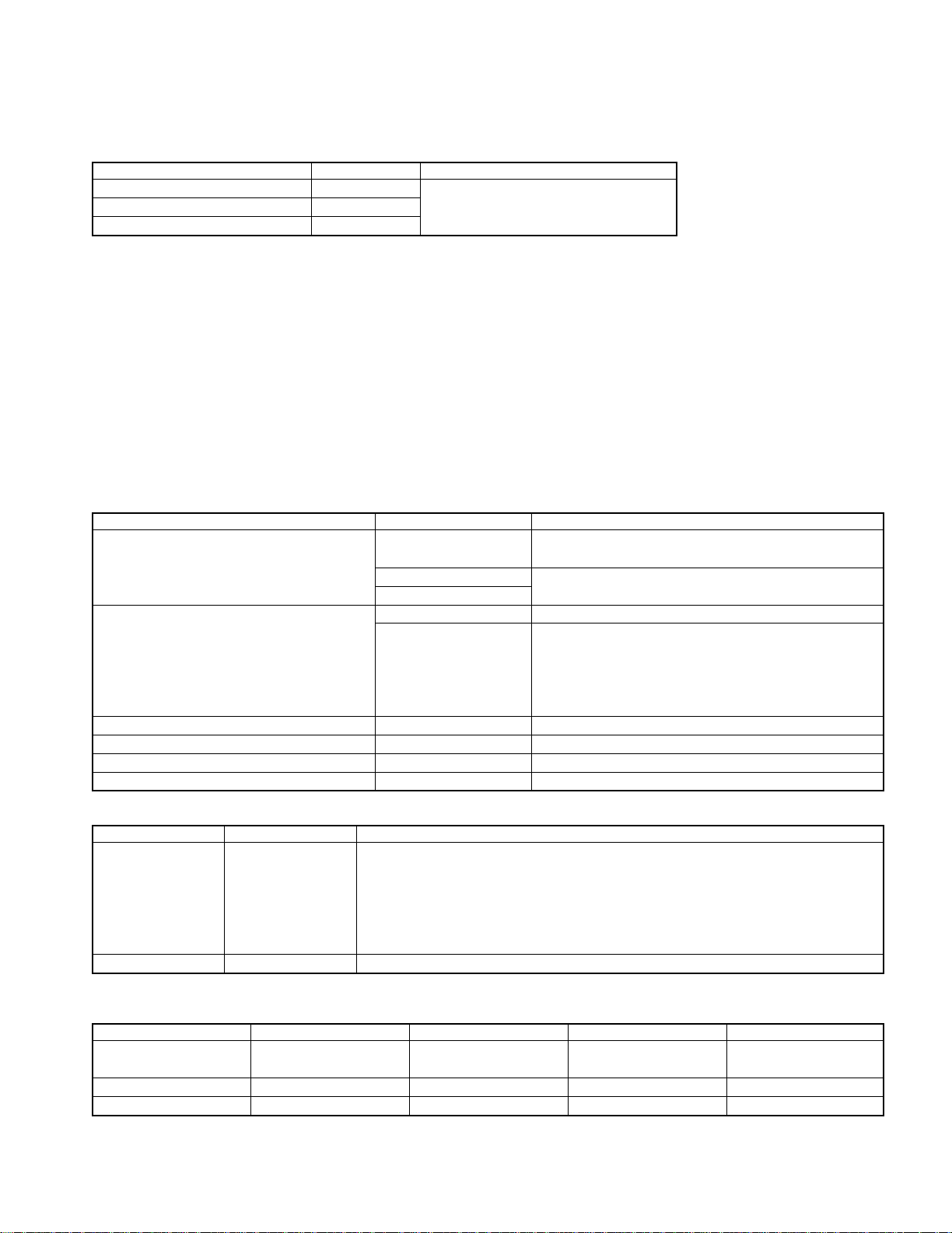
standby/timer
POWER
standby/timer
Operation to reset
The microcomputer may fall into malfunction (impossibility to operate, erroneous display, etc.) when the power
cord is unplugged while unit is ON or due to an external
factor. In this case, execute the following procedure to
reset the microcomputer and return it to normal condition.
Unplug the power cord from the power outlet, then while
holding the POWER or
key depressed, plug the power
cord again.
÷ Please note that resetting the microcomputer clears
the contents stored in and it returns to condition
when it left the factory.
or
After resetting the microcomputer, the display will show
as follow:
The marking of products using lasers (For countries other than U.S.A., U.S.-Military and Canada)
The marking of this product has been classified as Class 1. It means
that there is no danger of hazardous radiation outside the product.
Location: Back panel
CLASS 1
LASER PRODUCT
CAUTION
VISIBLE LASER RADIATION
WHEN OPEN. DO NOT STARE
INTO BEAM OR VIEW DIRECTLY
WITH OPTICAL INSTRUMENTS.
Inside this laser product, a laser diode classified as Class 3A laser
radiation is contained as alerted by the internal caution label shown
above. Do not stare into beam or view directly with optical instruments.
Location: CD laser pick-up unit cover inside this product
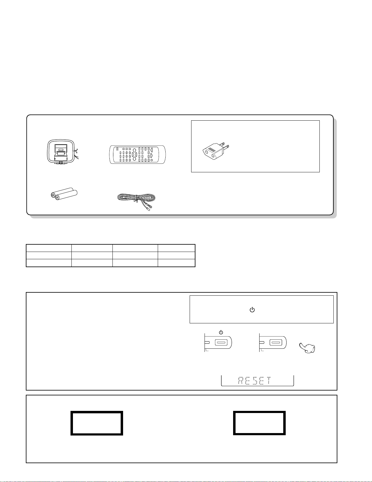
FM indoor antenna (1)
(T90-0855-05): V
(T90-0877-05): MM1XE
AM Loop antenna (1)
(T90-0852-05): V
(T90-0893-05): MM1XE
Batteries (R6/AA) (2)
Remote control unit (1)
(A70-1587-05): MM1XV
(A70-1588-05): E
AC Plug Adaptor (1)
(E03-0115-05)
Use to adapt the plug on the
power cord to the shape of the
wall outlet.
(Accessory only for regions where
use is necessary.)
RXD-M65V-H/M65V-N
CONTENTS / ACCESSORIES / CAUTIONS
Contents
CONTENTS / ACCESSORIES .................................. 2
EXTERNAL VIEW .......................................................3
DISASSEMBLY FOR REPAIR....................................4
BLOCK DIAGRAM ......................................................5
CIRCUIT DESCRIPTION ............................................6
ADJUSTMENT ..........................................................13
Accessories
INTERCONNECTION DIAGRAM .............................15
PC BOARD .............................................................. 16
SCHEMATIC DIAGRAM .......................................... 21
EXPLODED VIEW ....................................................28
PARTS LIST..............................................................30
SPECIFICATIONS ....................................................36
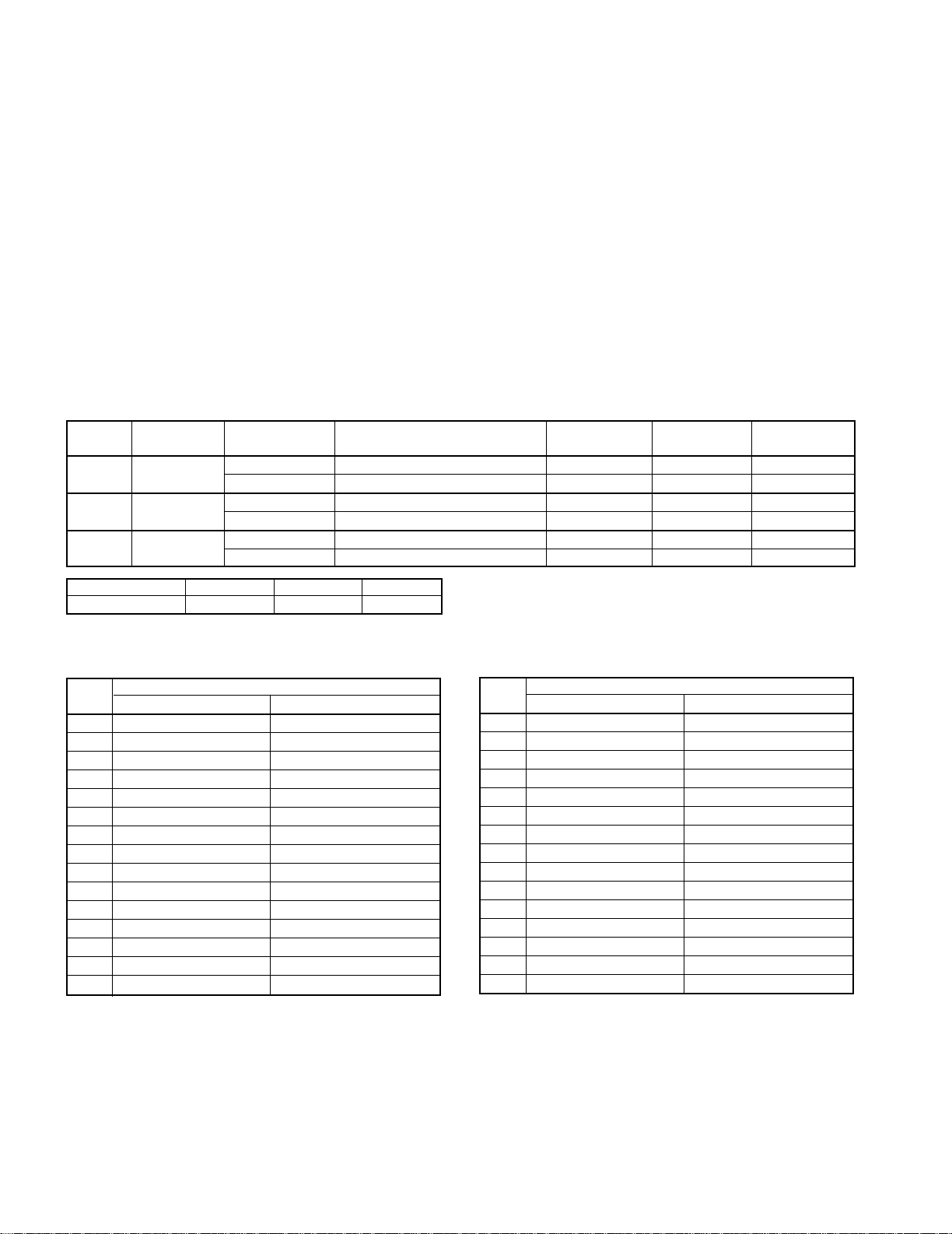
SYSTEM CONFIGURATIONS
SYSTEM MAIN UNIT DESTINATION SPEAKER
HM-V655MP-H RXD-M65V-H EMX LS-M65V-H
HM-V655MP-N RXD-M65V-N V LS-M65V-N
Cautions
2

DIGITAL
OUT
OPTICAL
AUX
OUT
L
R
FRONT
SPEAKERS
(6-16
Ω)
-
+
L
R
ANTENNA
GND
AM
FM
75
Ω
AUX
IN
VIDEO
OUT
AC 110 120V
~
AC 220 240V
~
Metallic cabinet *
(A01-)
Cover
(F07-1766-02)
RXD-M65V-H/M65V-N
EXTERNAL VIEW
Tuner ass'y *
(W02-)
Lock terminal board
(E70-0123-15)
Pin jack
(E63-1277-05)
Pin jack
(E63-1264-05)
Oscillating module
(W02-1114-15)
Slide switch *
(S62-0001-05)
AC power cord bushing *
(J42-)
AC power cord *
(E30-)
* Refer to parts list on page 30.
3

RXD-M65V-H/M65V-N
DISPLAY BOARD
Cushion
(not supplied)
REAR VIEW
Fig.1
Fig.2
Fig.3
DECK BOARD
FORWARD
REVERSE
DISASSEMBLY FOR REPAIR
How to open the CD tray when it does not come out.
1. Insert a flat driver in to a square hole on the mechanism as shown in
the figure.
2. Push a rack gear in the direction of arrow.
(At this time, the tray comes out slightly frontward.)
3. The tray can be opened by hand.
How to Adjust the Azimuth of the REC/PLAY Head
(To adjust the azimuth adjustment screws, it is necessary to
remove the front glass.)
1. Insert a screw driver into a hole on display board as shown in
the drawing. (Fig.1)
2. Push a driver frontward. (Fig.1)
3. Remove a front glass. (Fig.2)
4. Adjust the azimuth adjustment screws. (Fig.3)
* Replace a front glass if scratched.
4

0 to -78dB
MAIN VOL.1
BCLK
LRCK
SRDATA
TR KF
TR KR
FC SR
FC SF
SL DR
SL DF
SP DF
SP DR
SP DR
SL DRTR DR
FC DR
E
F
PDLDB
D
C
A
FE
TE
(ONLY E TYPE)
D. OUT
BEAT CANCEL
VR1.2
L1,2
AM
FM
V. OUT
A. OUT
REC/PLAY
REC-R
REC-F
PLAY-SW
PACK-SW
CPM
SOL
PHOTO
+9.0V
REC AMP
PB AMP
SA CLK
SA DATA
A.OUT
SA CE
PLL DO
SD
ST
INPUT VOL.
SELECTOR
CE
+
DATA
CLK
u-COM
CASSETTE DECK
PRE. AMP
FL DRIVER
TACT KEY
REMOCON. MODULE
STAND-BY LED
BACK-UP CIRCUIT
LED
ON/OFF
++
AC IN
X14,K401
+34dB
TUNER
-37.5V
VCD D+5V
VCD A+9V
VCD M+7.5V
-B
+B
AM 0dB=180mV
300mV
FM 0dB=600mV:75kDEV.
0dB=1.2V:1kHz
580mV
TAPE 0dB
+++
AUX
CD
TUNER
INPUT VOL.
0dB
0dB
0dB
300mV
MAIN VOL.2
0 to -18dB
+
A.MUTE ON/STANDBY
FL DRIVER
37.5V
+
DSP MPEG DECODER
X14,
IC3
AN22000A
RF-AMP
CD MECHA
4ch DRIVER
AN4801SB
IC4
DAC
RDS IC
X29,IC801
X14,IC501
FL DRIVER
ED501
FL
X29,IC202
PRE. AMP
AUX OUT
DECK MECHA
X29,A601
IC1
SERVO u-COM
MN6627482WA
IC2
DIGITAL OUT
VIDEO OUT
BIAS ADJ.
ERASE
REC/PLAY
Q15-18
OSC
BIAS
BIAS
TRAP
ATT.
AUX IN
AUX OUT
X29,J602
X29,J601
TUNER PACK
-8dB
IC701
X29,
IC6
DAC
ES3883
TV ENCODER
ES3800FL
IC5
Q5
HA12230NT
KEY
X14,S516
X14,A501
ROTARY ENCODER
REMOCON MODULE
u-COM
MAIN
LED
OUT
REC
E.VOL
X29,IC601
IC1
X29,IC101
FIL
X29,Q10
RELAY
PRIMARY
+5.4V
X14,IC402
AVR
AVR
+5V
+9V
AVR
X14,D403
X29,D4
X29,Q111-114
POWER AMP
X29,Q106
PROTECTION
AMP
AUX IN
POWER AMP.
X29,IC911
AVR
+5V
CD
AUX OUT
TAPE REC
TUNER
TAPE PLAY
0dB
X29,IC910
+9V
AVR
X29,D900
AVR
-30V
X29,Q13
X29,D3
VOL.
INPUT
VOL.
FLAT
EX BASS
GAIN DISTRIBUTION
LOUDNESS
LC75343M
E.VOL
BASS,MID,TRE
10dB
TONE
Q1,2
50W : 6ohm
EIAJ 10%
K1
1kHz
J2
HEAD-
OUT
PHONE
W02-2920-15 (E TYPE)
W02-2919-15 (M,X,V TYPE)
(W02-2949-05)
VCD MODULE
(X28- )
RXD-M65V
5
BLOCK DIAGRM
RXD-M65V-H/M65V-N
RXD-M65V-H/M65V-N
CIRCUIT DESCRIPTION
1. Initializing
1-1 Initializing Method
• While holding down the [POWER] key, plugged in the power cord to AC power wall outlet.
1-2 Initializing Operation
• During the initial operation, the display shows "RESET "and after that
• it will be returned to standby condition.
• If any mechanisms error occurred, the error indication is displayed as "ERR" in the display.
1-3 Mechanism Initializations
1 CD Mechanism
• If a mechanism error occurred, the error indication is displayed as "C ERR " in the display.
2 Deck Mechanism
• If a mechanism error occurred, the error indication is displayed as "X ERR " in the display.
2. Tuner Destination
Set Destination Band Receiving Frequency Range
E/T/H E3 FM 87.5MHz~108.0MHz 50kHz +10.7MHz 25kHz
E2 RDS AM 531kHz~1602kHz 9kHz +450kHz 9kHz
M/X/V/I E1
M/V/I K2
FM 87.5MHz~108.0MHz 50kHz +10.7MHz 25kHz
AM 531kHz~1602kHz 9kHz +450kHz 9kHz
FM 87.5MHz~108.0MHz 100kHz +10.7MHz 25kHz
AM 530kHz~1610kHz 10kHz +450kHz 10kHz
Channel
Space
IF RF
Type E/E2/T/H M/V X
✽ Voltage Range 4.2V~5.0V 1.4V~2.5V 0.7~1.3V
✽ Pin 3 of microcomputer (X29, IC701).
3. Tuner Preset Frequency
P.CH
1 FM 98.30MHz FM 98.30MHz
2 FM 108.0MHz FM 108.0MHz
3 FM 89.10MHz FM 89.10MHz
4 FM 87.50MHz FM 87.50MHz
5 FM 90.00MHz FM 90.00MHz
6 FM 87.50MHz FM 87.50MHz
7 FM 87.50MHz FM 87.50MHz
8 FM 87.50MHz AM 1503kHz
9 AM 1610kHz AM 1584kHz
10 AM 1000kHz AM 999kHz
11 AM 630kHz AM 621kHz
12 AM 1440kHz AM 1350kHz
13 FM 106.0MHz FM 106.0MHz
14 AM 530kHz AM 531kHz
15 FM 87.50MHz FM 87.50MHz
K2(M,V TYPE) E1/E3(E,E2,T,H,M,V,X)
Frequency
P.CH
16 FM 98.00MHz FM 98.00MHz
17 FM 98.50MHz FM 98.50MHz
18 FM 87.50MHz FM 87.50MHz
19 AM 990kHz AM 945kHz
20 FM 97.40MHz FM 97.40MHz
21 AM 530kHz AM 531kHz
22 FM 87.50MHz FM 87.50MHz
23 FM 87.50MHz FM 87.50MHz
24 FM 87.50MHz FM 87.50MHz
25 FM 87.50MHz FM 87.50MHz
26 FM 87.50MHz FM 87.50MHz
27 FM 87.50MHz FM 87.50MHz
28 FM 87.50MHz FM 87.50MHz
29 FM 87.50MHz FM 87.50MHz
30 FM 106.0MHz FM 106.0MHz
K2(M,V TYPE) E1/E3(E,E2,T,H,M,V,X)
Frequency
6
RXD-M65V-H/M65V-N
CIRCUIT DESCRIPTION
4. Test Mode
4-1 Setting method of the Test Mode
Test Mode Keys Setting Method
CD MODE CD PLAY key
DECK MODE TAPE PLAY
* SUB CLOCK OSC DIAGNOSIS MODE key
* The oscillation diagnosis (existence of oscillation and measurement of period) of a sub clock is performed
before the test mode is entered. If the diagnosis result is OK, the system enters the test mode.
If the diagnosis result is NG, the oscillation of the sub clock is diagnosed again. If the result is OK, the system
enters the test mode. If the diagnosis result is continuously NG 5 times, the system stops with "ERR1"and
"ERR2"displayed.
4-2 Cancel of the test mode
• Initialized and cancel the test mode if pulling out the power cord.
• Cancel the test mode only if the power key is turned off.
4-3 Contents of the Test Mode
• The muting during mode selection is not controlled in the test mode.
• During the test mode, it can be operated in a special manner that is different from an ordinary
operation by using the keys on the main body, specifically as shown in the following tables.
Insert the AC cord to AC wall
outlet while holding down the left key.
4-4 CD Test Mode
Keys Display Operation
CD-PLAY/PAUSE 05
(Cyclically changed the mode (✽✽:✽✽)Time Display • Pickup moves inward.
05 and 03 by pressing the key.) 03 ✽ ✽:✽ ✽ • Tracking-servo off. (for checking TE)
(✽ ✽:✽ ✽)Time Display • Pickup moves outward.
CD STOP 00 : 00 Stop the CD operation.
(Cyclically changed in the stop mode only.) 07 FG/FE FG value /FE value
SKIP UP Ex.01~02 • Track number up.
SKIP DOWN Ex.02~01 • Track number down.
SKIP UP Usual Indication • Play the first track number in the stop mode.
SKIP DOWN Usual Indication • Play the last track number in the stop mode.
✽ ✽:✽ ✽ • Tracking-servo on.
Adjustment value/mean value
08 FB/FO FBAL value /FO value
09 TG/TE TG value /TE value
10 TB/TO TBAL value /TO value
4-5 Deck Test Mode
Keys Display Operation
• 4 Seconds Recording
If the REC/ARM key is pressed, the system record for 4 seconds.
Then, it rewinds to the REC starting position and plays back automatically.
TAPE REC TAPE If the REC/ARM key is pressed, during the 4 seconds REC operation, the
system records further for 4 seconds, then returns to the starting position
of the first 4 seconds REC operation and plays back.
SOUND Beat-C ON Beat cancel will be on while pressing the sound key.
✽
Mechanism half switches indication
The mechanism half switches status are indicated "blank" or "E "in the display.
8th Dot(Display) 1st figure 2nd figure 3rd figure 4th figure
Mechanism FWD REC Inhibit RVS REC Inhibit Cassette Half Tape Play
Half Switch Detection SW Detection SW Detection SW Detection SW
ON Blank Blank Blank Blank
OFF E E E E
7

RXD-M65V-H/M65V-N
X28,IC1
DECK SYSTEM IC
HA12230NT
X14,IC501
FL DRIVER
(MN12510F)
DECK MECHA.
X14,ED501 X29,IC601
(HNA-14MS07T)
Vaccume Fluorescent
Display
(LC75343M)
SYSTEM IC
X29,IC701
MN101C51FGD
TUNER ASSY
VCD MODULE
(W02-2949-15)
PLL IC
X29,IC801
RDS IC (E/T TYPE)
(BU1923F)
KEY REMOTE ENCODER
KEY1,2 X14,A501 X14,S516
CIRCUIT DESCRIPTION
5. Microcomputer : MN101C51F (X29, IC701)
5-1 Microcomputer Periphery Block diagram
Key Matrix VREF =5.0V
Voltage
Range
Key 1 ON/
(Pin 5) STANDBY DOWN PLAY UP OPEN
Key 2
(Pin 6) PLAY
0 0.89 1.55 2.00 2.61 3.02 3.47 3.95 5.00
AUX TUNER
REC SET MODE O.T.E.
SKIP
STOP
TAPE
CD SKIP CD
REPEAT SOUND (off)
(off)
8

RXD-M65V-H/M65V-N
CIRCUIT DESCRIPTION
5-2 Pin Description of Microcomputer
Pin No. Pin Name I/O Pin Description
1 VREF- - Power supply (-) for A/D converter.
2 PH I Deck reel sensor input.
3 TN TYPE I Discrimination of tuner destination.
4 S LEVEL I RDS signal level input. (E/T version only)
5,6 KEY1,KEY2 I A/D key (1, 2) input.
7 A LEVEL I Unused.
8 TH I Unused.
9 CD PROTECT I Detection pin of CD protection.
10 VREF+ - A/D reference voltage input of the A/D converter.
11 VDD I Pin for power supply (+5V).
12 OSC2 O Main clock output (8.388MHz).
13 OSC1 I Main clock input (8.388MHz).
14 VSS - Connected to be ground.
15 XI I Timer clock input (32.768kHz).
16 XO O Timer clock output (32.768kHz).
17 MMOD - Connected to be ground.
18 SDI O Data output to FL driver.
19 SDO I Data input from FL driver.
20 SCK O Clock output to FL driver.
21~23 N.C. - Unused.
24 CL SW I Input pin of close switch for CD tray. Closed
25 RESET I Reset signal input for microcomputer. Reset
26 CE I Back up detection input. AC On AC Off
27 OP SW I Input pin of open switch for CD tray. Opened
28 CD POWER O ON/OFF control pin for CD DSP power.
29 N.C. - Unused.
30 VCD u-com ACK I/O DSA Acknowledge
31 REM CONTROL I Remote control signal input.
32 NO USE - Unused.
33 RDSCLK I RDS clock input. (E/T version only)
34 RESET2 I Detection pin of voltage drop.
35 NO USE - Unused.
36 PAL/NTSC O TV system selector AUTO
37 VCD u-com DATA I/O DSA data pin for ESS.
38 VCD u-com ST I/O DSA STB pin for ESS.
39 CLOSE O Control pin of CD tray motor to close the tray.
40 OPEN O Control pin of CD tray motor to open the tray.
41 HP IN I Detection pin for headphones jack. Detected
42 FLASH UC 1 I Power supply for flash ROM.
43 FLASH UC 2 I Power supply for flash ROM.
44 EVOL CE O Chip enable output to electronic volume (X29, IC601).
45 EVOL.CLK O Clock output to electronic volume (X29, IC601).
46 EVOL.DATA O Data output to electronic volume (X29, IC601).
47 POWER RLY O Power relay control.
48~51 N.C. - Unused.
52 PLL CLK O PLL IC clock output.
53 PLL DO/ST I PLL IC data input.
54 PLL DAT O PLL IC data output.
55 PLL CE O PLL IC chip enable output.
56 SD I SD detector input. Detected
57 TU MUTE O Tuner mute control. Mute ON
58 PLAY SW I Detection switch input of head position for deck. Playback
Active
HL
9

RXD-M65V-H/M65V-N
CIRCUIT DESCRIPTION
Pin No. Pin Name I/O Pin Description
59 REC R SW I Deck reverse recording switch input. OFF ON
60 REC F SW I Deck forward recording switch input. OFF ON
61 HALF SW I Cassette half switch input. Detected
62 BEAT C O ON/OFF control pin of beat cancel for deck. ON OFF
63 R/P O Deck recording & playback changeover. Recording Playback
64 BIAS O ON/OFF control pin of bias for deck. ON OFF
65 A/B-1 O Deck recording mute & head select control 1.
66 A/B-2 O Deck recording mute & head select control 2.
67 MUTE O Deck line mute control. ON
68 CPM O Control pin of capstan motor for deck.
69 SOL O Control pin of solenoid for deck.
70 RDS DATA I RDS data input. (E/T version only)
71 PROTECT I Detection pin of the protection for power supply.
72 AMUTE O Audio mute output.
73 SP RLY O On/off control pin for speaker relay.
74 EEP SDA I/O EEPROM data input/output.
75 EEP SCL O EEPROM clock output.
76,77 ENC A,B I Volume encoder (X14, S516) signal inputs.
78 LED STBY RED O Standby led (red) control pin. OFF ON
79 LED STBY GRN O Standby led (green) control pin. OFF ON
80 NCS O Chip enable output of FL driver.
Active
HL
6. Pin Description of IC's
6-1 CD Motor Driver : TA8409S (X29, IC26)
Pin No. Pin Name I/O Pin Description
1 IN2 I Input pin.
2 VCC - Power supply.
3 OUT2 O Output pin.
4 NC - Unused.
5 GND - GND
6 VS - Power supply for output side.
7 OUT1 O Output pin.
8 VREF - Control power supply.
9 IN1 I Input pin.
Function
INPUT OUTPUT MODE
IN 1 IN 2 OUT 1 OUT 2 MOTOR
00∞∞ STOP
1 0 H L CW/CCW
0 1 L H CCW/CW
1 1 L L BRAKE
∞ : High Impedance
Note) Input : "H" Active
10
 Loading...