Kenwood RX-DM51-MD, HM-531, HM-581-MD Service Manual

MICRO HiFi COMPONENT SYSTEM
MD 6
TUNER
micro hi-fi component systemAuto Reverse
AUX
push
OPEN
MD rec
DISC LOADING MECHANISM
TAPE/preset
band
1BIT DUAL D/A CONVERTER
TAPE rec
remote
TAPE
direction
set/demo
menu
repeat
sound
standby/timer
on/standby
3
d
o
w
n
u
p
2
V
O
L
U
M
E
/
m
u
l
t
i
c
o
n
t
r
o
l
phones
CD 6
74
1¡
¢
0
0
2 3
RXD-M51/M51MD
SERVICE MANUAL
(HM-531/581MD)
© 1998-9/B51-5477-00 (K/K) 2138
Dressing panel
(A21-3707-03)
Knob
(K29-7392-02)
Dressing panel
(A21-3721-03)
Panel (MD)
(A29-1022-04)
Front glass
(B10-3418-03)
Panel
(A60-1496-11)
Knob
(K29-7393-03)
Knob
(K29-6358-14)
Indicator
(B12-0351-03)
Knob
(K29-7394-03)
Front glass
(B10-3419-14)
• Refer to DM-3090 service manual(B51-5396-00), if
require the following items in detail.
1) MD mechanism(MDM-98A) disassembly for repair
(page5,6)
2) Semiconductor description
IC1101:RF signal control(page9)
IC1201:ENDEC/ATRAC(page10,11)
IC1401:system microcomputer(page 12,13)
Miniature phone jack
(E11-0344-05)
Illustration is RXD-M51MD.
* Refer to parts list on page 49.
Caution : No connection of ground line if disassemble the
KENWOOD-Crop. certifies this equipment conforms to DHHS
Regulations No. 21 DFR 1040. 10, Chapter 1, Subchapter J.
DANGER : Laser radiation when open and interlock defeated.
AVOID DIRECT EXPOSURE TO BEAM
unit.
Please connect the ground line on rear panel,
PCBs, Chassis and some others.
SYSTEM MAIN UNIT DESTINATION SPEAKER SP CORD PARTS.NO.
HM-581MD RXD-M51MD E1T1 LS-M61 E30-5500-05
HM-531 RXD-M51 M1E2T2 LS-M51 E30-5500-05
Operation to reset
The microcomputer may fall into malfunction (impossibility to operate, erroneous display, etc.) when the power
cord is unplugged while unit is ON or due to an external
factor. In this case, execute the following procedure to
reset the microcomputer and return it to normal condition.
Unplug the power cord from the power outlet then, while
holding the “set/demo” key depressed, plug the power
cord again.
÷ Please note that resetting the microcomputer clears the
contents stored in and it returns to condition when it left
the factory.
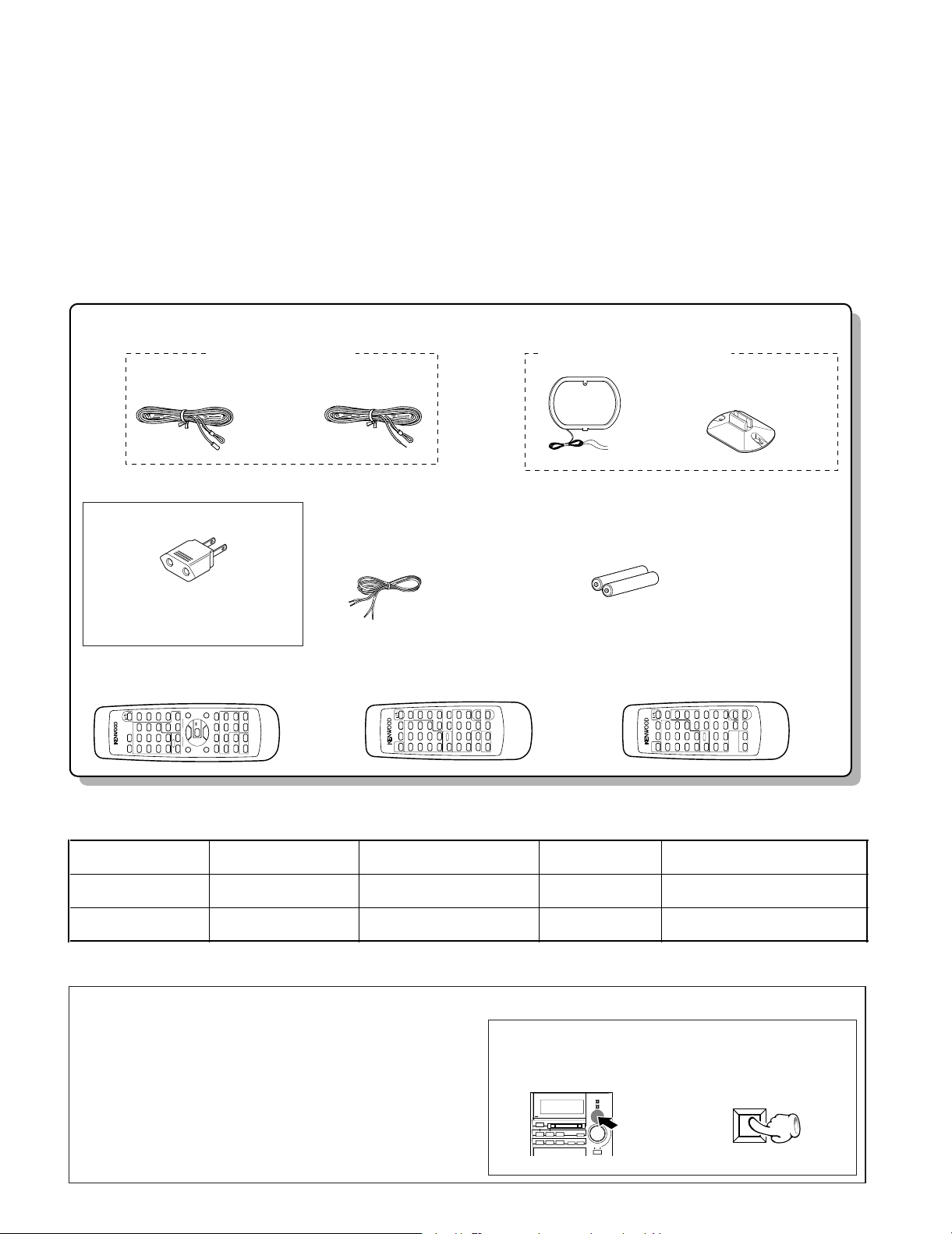
Batteries (R6/AA) (2)
Other countries
Remote control unit (1)
AM loop antenna stand (1)
Speaker cords (2)
Loop antenna (1) (T90-0833-05)
Please confirm that the following accessories are present.
FM indoor antenna (1)
Europe U.K. and Russia
AC plug adapter (1)
Use to adapt the plug on the power
cord to the shape of the wall outlet.
(Accessory only for regions where
use is necessary.
(T90-0810-05): TE
(E03-0115-05)
(E30-5500-05)
(A70-1236-05) : RC-M0503E
Remote control unit (1)
(A70-1242-05) : RC-F0503E
Remote control unit (1)
(A70-1241-05) : RC-F0503
(T90-0801-05): M
(J19-3645-05))
¢
REMOTE CONTROL UNIT
RC-F0503E
SLEEP TONE SOUND
1 2 3 TIMER
4 5 6 REPEAT
7 8 9
RANDOM
+10 0 PGM CLEAR
DOT DISP.TIME DISP.
TAPE
P.CALL
TAPE
TUNER
BAND
CD
PTY
TA/NEWS
AUX
SET ENTER MUTE
¡4
2 3 7
%
fi
6
1
POWER
VOLUME
O.T.E.
TRACK
EDIT
TITLE
INPUT
TITLE
SEARCH
TIMER
RANDOM
CLEAR
DELETE
REPEAT
6
CD
6
TUNER
BAND
SET
DOT/CHARA.
TIME ENTER
SLEEP
1 2 3
4 5 6
7 8 9
+10 0
DOLBY NR
QUICK
MOVE
TAPE
PTY
TA/NEWS
AUX
¢
P.CALL
4
2 3
PGM
¡1
REMOTE CONTROL UNIT
RC-M0503E
SOUNDTONEMDTAPE
MD
7
%
fi
MUTE
V
O
L
U
M
E
C
O
N
T
R
O
L
DISPLAY
O.T.E.
POWER
¢
REMOTE CONTROL UNIT
RC-F0503
SLEEP TONE SOUND
1 2 3 TIMER
4 5 6 REPEAT
7 8 9
RANDOM
+10 0 PGM CLEAR
DOT DISP.TIME DISP.
TAPE
P.CALL
TAPE
TUNER
BAND
CD
AUX
SET ENTER MUTE
¡4
2 3 7
%
fi
6
1
POWER
VOLUME
O.T.E.
RXD-M51/M51MD
CONTENTS / ACCESSORIES / CAUTION
Contents
CONTENTS / ACCESSORIES / CAUTION.................2
EXTERNAL VIEW/DISASSEMBLY FOR REPAIR.......3
BLOCK DIAGRAM.......................................................4
CIRCUIT DESCRIPTION.............................................5
ADJUSTMENT.......................................................... 11
WIRING DIAGRAM....................................................12
Accessories
PC BOARD ................................................................13
SCHEMATIC DIAGRAM............................................23
EXPLODED VIEW .....................................................45
PARTS LIST...............................................................49
SPECIFICATIONS.....................................................59
System configuration
Caution
2
set/demo
1
2
3
EXTERNAL VIEW / DISASSEMBLY FOR REPAIR
EXTERNAL VIEW
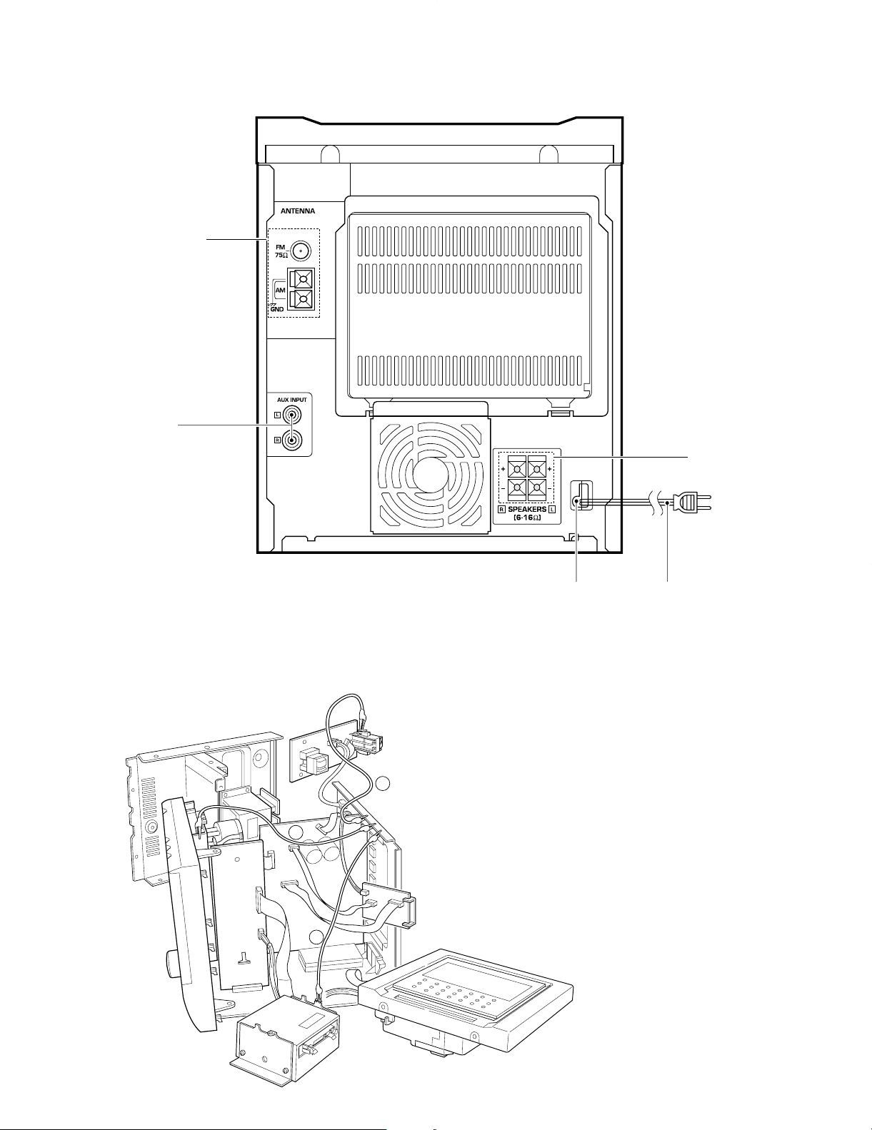
Lock terminal board
(E70-0052-05)
Phono jack
(E63-1024-05)
RXD-M51/M51MD
Lock terminal board
(E70-0053-05)
DISASSEMBLY FOR REPAIR
Power cord bushing
(J42-0083-05)
AC power cord *
(E30-)
Illustration is RXD-M51MD.
* Refer to parts list on page 49.
< How to check the PCB >
See the left figure, connect the SP terminal GND and the rear
panel (1), the front panel GND and the rear panel (2), MD
mecha chassis and the rear panel (3) (except RXD-M51) with
the wires connected alligator chips.
3
4
(X33)
(X14)
ONLY
(X09)
A301 (W02-)
(X14)
ONLY
E,T TYPE
(X33)
(X07)
RXD-M51MD
RXD-M51
RXD-M51
ONLY
RXD-M51MD
200mV/47k
AUX IN
AUX IN
ATT
3dB
FM
AM
ANT
TUNER PACK
ERASE
R/P
BIAS TRAP
MPX
OSC
BIAS
Q11,12
IC1
IC2
IC3
FE-BIAS
VR201
(RF-AMP)
CXA1571M
IC203
CXD2587Q
(DSP/DAC/CD-TEXT)
IC201
(4ch BTL-DRIVER)
BA5979S
IC202
MECHA.
CD
DIGITAL OUT
UPD7805BGC-A59
MD MECHA.
IC1
DIGITAL IN
(LEVEL SHIFT)
TC74HCT7007AF
RDS
(MAIN u-COM)
IC205
IC206
REMOTE FL
FL
DRIVER
(A/D)
KEY
ENCODER
ROTARY
C0NTROL
LED
MID
TREBLE
BASS
EX. BASS
LOUD
J1
HEADPHONES
AMP
POWER
D1
38V
AVR
D2
+12V
AVR
+8V
AVR
D3
P. T.
T1
+5.6V
AVR
D16-21
DECK MECHA
DECK ANALOG
TUNER
AUDIO
CD BTL-DRIVER
MD ANALOG
MD MECHA. DIGITAL
CD DSP. RF-AMP
FL DRIVER DISPLAY
MD u-COM
MAIN u-COM
IC1
S1 Q1-6
IC2
A1
IC3
MD MECHA.
MDM-98A
IC5
IC4
Q3,4
Q5-16
PROTECTION
CIRCUIT
Q17-21
FL
Q32,35
Q27-29
Q30,31
+5V
AVR
Q208
Q205
+5V
AVR
Q7,8
AVR
+6.5V/5V
Q9
AVR
+6V
+5V
AVR
Q201,202
FL FILAMENT
AC4.5V
K1
POWER
RELAY
Q33
AC IN
DIGITAL OUT
A201
DECK
SP. OUTPUT
M,E,T 12.25V/6 (10%)
POWER RELAY
J1
CONTROL u-COM
L3,4
SPEAKERS
D5
ED1
MECHA.
DECK
425mV
FE
TE
SI
RF
FFDR
FRDR
TFDR
TRDR
SFDR
SRDR
MDP
Rch-OUT
Lch-OUT
PB AMP
REC AMP
DOLBY B
OUT 580mV
IN
R/P (REC=H)
DOUT
RESET
(FCS.TRK.SLD.SFD-DRIVE)
DSCK
RESET
PDOWN
MD-ST
SERCH
KDATA
U.T.D
U.K.D
X1
X1
X2
DSTB
MDDATA
LOAD SW
MD R.D
MD T.D
+
+
+
+
+
5.0V
3.3V
1.2V1.8V
+3dB
MUTE
200mV
DOLBY
DECK
TUNER
AUX
CD
MD
850mV
+12V
(5MHz)
850mV
RXD-M51/M51MD
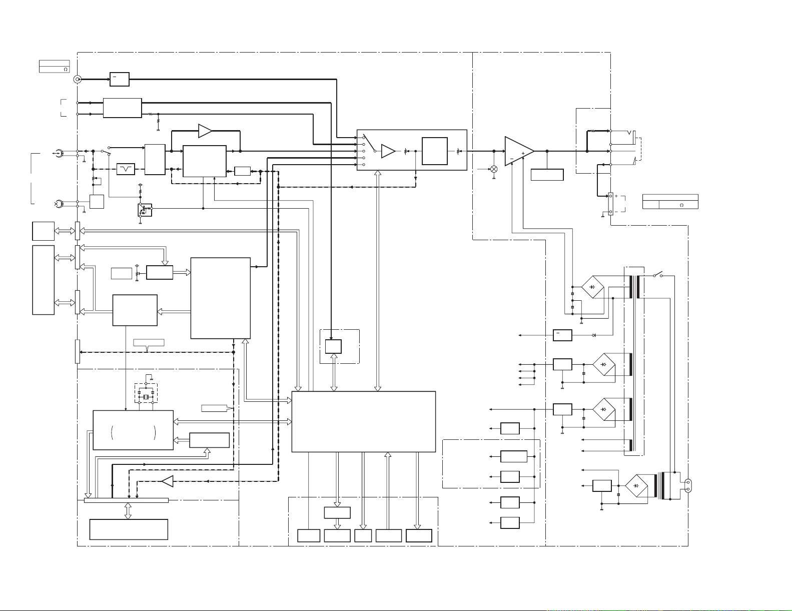
BLOCK DIAGRAM
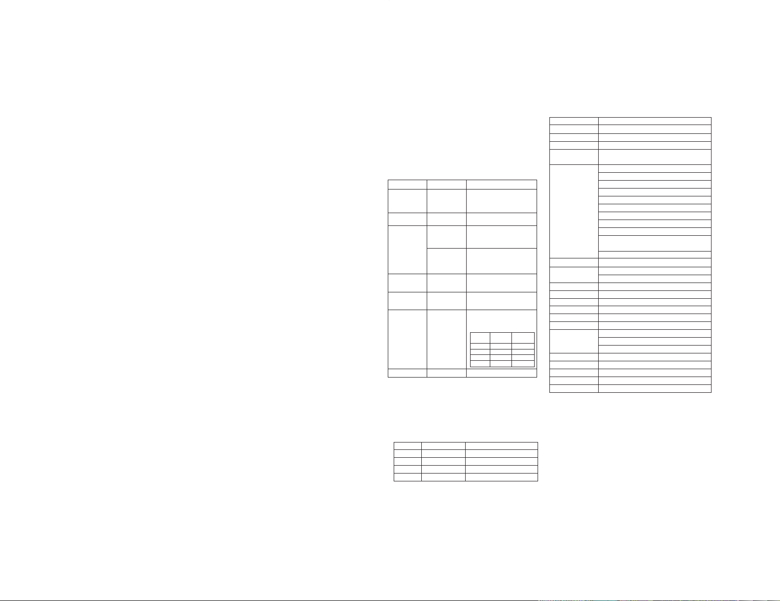
1. Initialization
1-1 Setting of initial conditions
While pressing the [SET] key, plug the AC power cord
into an AC power outlet.
1-2 Initializing operation
• A microcomputer is initialized for start when the AC
power is turned on while pressing the [SET] key. At
that time, CD mechanism, MD mechanism and CASSETTE mechanism are also initialized.
• During the initial operation, the display shows “INITIALIZE” and after that the clock blinks up on display.
1-3 Initial items and back up data
1-4 Mechanism initialization
1-4-1 CD mechanism
• If a mechanism error occurs, “C” is indicated on the
display.
1-4-2 MD mechanism
• The MD ON code is input within 4 seconds after turned
the power port on, the MD initial code (D122H) is output.
If the MD on code is not input, the error indication is
displayed as "M" on the display.
1-4-3 CASSETTE mechanism
• If a mechanism error occurs, "X" is indicated on the display.
ch
Destination
K2 E2 E1/H
1 FM 97.50MHz FM 97.50MHz FM 97.50MHz
2 FM 108.00MHz FM 108.00MHz FM 108.00MHz
3 AM 630kHz AM 630kHz AM 630kHz
4 AM 1000kHz AM 999kHz AM 999kHz
5 AM 1440kHz AM 1440kHz AM 1440kHz
6 AM 1610kHz AM 1602kHz AM 1602kHz
7 FM 87.50MHz FM 87.50MHz FM 87.50MHz
8 FM 87.50MHz FM 87.50MHz FM 87.50MHz
9 FM 87.50MHz FM 87.50MHz FM 87.50MHz
10 FM 89.10MHz FM 89.10MHz FM 89.10MHz
11 FM 87.50MHz FM 87.50MHz FM 87.50MHz
12 FM 90.00MHz FM 90.00MHz FM 90.00MHz
13 FM 106.00MHz FM 106.00MHz FM 106.00MHz
14 AM 530kHz AM 531kHz AM 531kHz
15 FM 87.50MHz FM 87.50MHz FM 87.50MHz
16 FM 98.00MHz FM 98.00MHz FM 98.00MHz
17 FM 98.50MHz FM 98.50MHz FM 98.50MHz
18 FM 87.50MHz FM 87.50MHz FM 87.50MHz
19 AM 990kHz AM 990kHz AM 990kHz
20 FM 97.40MHz FM 97.40MHz FM 97.40MHz
21 FM 87.50MHz FM 87.50MHz FM 87.50MHz
22 FM 87.50MHz FM 87.50MHz FM 87.50MHz
23 FM 87.50MHz FM 87.50MHz FM 87.50MHz
24 FM 87.50MHz FM 87.50MHz FM 87.50MHz
25 FM 87.50MHz FM 87.50MHz FM 87.50MHz
26 FM 87.50MHz FM 87.50MHz FM 87.50MHz
27 FM 87.50MHz FM 87.50MHz FM 87.50MHz
28 FM 87.50MHz FM 87.50MHz FM 87.50MHz
29 FM 87.50MHz FM 87.50MHz FM 87.50MHz
30 FM 87.50MHz FM 87.50MHz FM 87.50MHz
31 FM 87.50MHz FM 87.50MHz FM 87.50MHz
32 FM 87.50MHz FM 87.50MHz FM 87.50MHz
33 FM 87.50MHz FM 87.50MHz FM 87.50MHz
34 FM 87.50MHz FM 87.50MHz FM 87.50MHz
35 FM 87.50MHz FM 87.50MHz FM 87.50MHz
36 FM 87.50MHz FM 87.50MHz FM 87.50MHz
37 FM 87.50MHz FM 87.50MHz FM 87.50MHz
38 FM 87.50MHz FM 87.50MHz FML 74.00MHz
39 FM 87.50MHz FM 87.50MHz FML 65.00MHz
40 FM 87.50MHz FM 87.50MHz FML 69.00MHz
2. TUNER preset frequency
ITEMS
POWER OFF
VOLUME 15
BALANCE CENTER
LOUDNESS OFF
AMP EX. BASS ON
INPUT SEL TUNER
AUX INPUT 0 (-6dB)
BASS 0
TREBLE 0
BAND FM
LAST f LIMIT
TUNER LAST Pch
AUTO/MONO AUTO
Pch TEST f
CLOCK AM 12 : 00
PROG ON AM 12 : 00
CLOCK PROG OFF AM 12 : 00
TIMER PRO MODE PLAY
SOURCE TUNER
Pch 1
EXE OFF
OTT OFF
SLEEP OFF
PLAY MODE TRACK
REPEAT OFF
CD RANDOM OFF
PLAY MODE STOP
TIME SINGLE
DIRECTION FORWARD
DECK RVS MODE p
DOLBY NR OFF
OPERATION MODE STOP
back up data
4. Main microprocessor M30622MA-174FP (X09 : IC205)
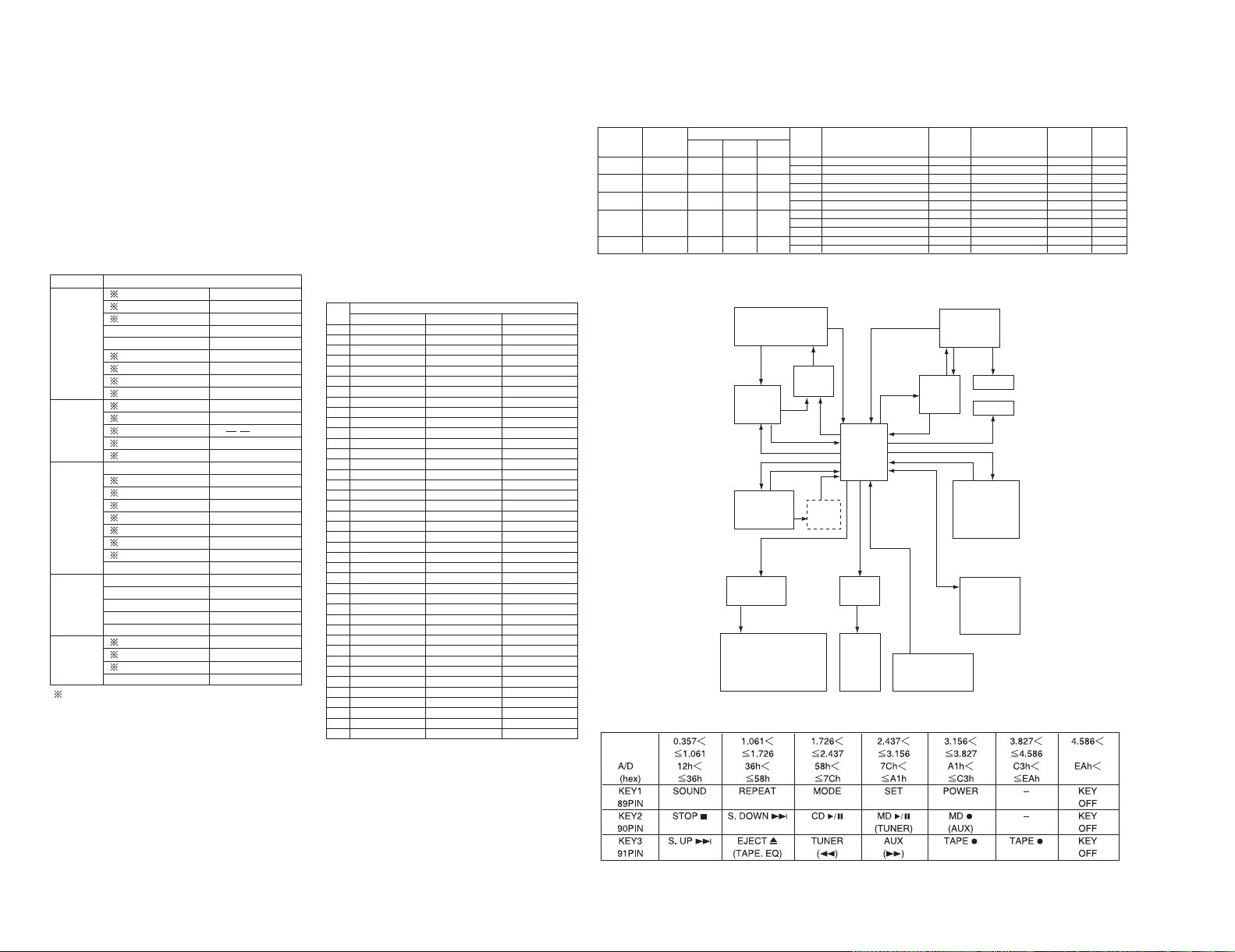
4-1 Microprocessor periphery block diagram
4-2 Key matrix
Vref = 5V ( ) of KEY : RXD-M51
Desti-
U-COM Discrimination
Receiving frequency Channel PORT
nation
Desti-
DSW4 DSW3 DSW2
Band range space
IF RF
92
nation
K, P K1 0 0 0
FM 87.5MHz~108.0MHz 100kHz +10.7MHz 25kHz 0
AM 530kHz~1700kHz 10kHz +450kHz 10kHz 0
M, Y K2 0 1 1
FM 87.5MHz~108.0MHz 100kHz +10.7MHz 25kHz 1
AM 530kHz~1610kHz 10kHz +450kHz 10kHz 0
JJ00
FM 76.0MHz~108.0MHz 100kHz -10.7MHz 25kHz 0
AM 531kHz~1629kHz 9kHz +450kHz 9kHz 0
Q
FMH 87.5MHz~108.0MHz 50kHz +10.7MHz 10kHz 0
Q
RDS
1 0 FML 65.0MHz~74.0MHz 10kHz +10.7MHz 10kHz 0
AM 531kHz~1602kHz 9kHz +450kHz 9kHz 0
E, T
E1
110
FM 87.5MHz~108.0MHz 50kHz +10.7MHz 25kHz 0
RDS AM 531kHz~1602kHz 9kHz +450kHz 9kHz 0
3. Destination list of TUNER
(DSW4=50pin, DSW3=49pin, DSW2=48pin)
0=(input low) 1=(input high)
GC-E6003
X09,
IC203
X14, IC1
X14
Q1~6
X09
IC4
X09
IC1
X09, IC2
X09
A301
X09
IC206
E TYPE
ONLY
X09
IC205
CD mechanism
Mechanism
control
circuit
Mechanism
control
circuit
Auto reverse
cassette
mechanism
Head amp
Dolby B
CXD2587Q
CD-DSP
TUNER
PLL IC
LC72131M
AUDIO
AMP SYSTEM IC
(LC75396)
MD
MDM-98A
LED
X14 ED1
FL
CM1740M
Key matrix
encoder
remocon
RDS
demodulator
DOT driver
LC75710NED
LED driver
M30622MA-174FP
u-COM
VOLTAGE
[V]
CIRCUIT DESCRIPTION
RXD-M51/M51MD
5
6
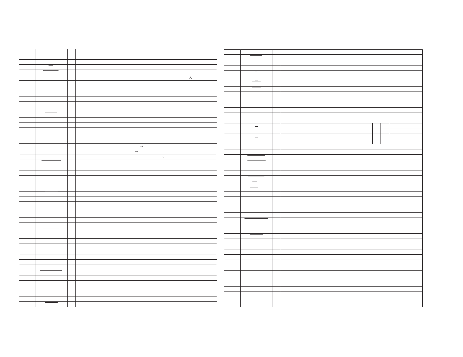
Pin No. Name I/O Description
1 CE O SYSTEM IC(LC75396)/PLL IC(LC72131) CE
2 PLL DO I PLL DATA INPUT
3 SD I TUNER SD DETECT INPUT H : NO TUNED L : TUNED
4 STEREO I TUNER STEREO DETECT INPUT H : MONO L : STEREO
5 EMPHASIS O TUNER EMPHASIS CHANGEOVER H : FM100kHz L : AM 50kHz
6 RDS DATA I RDS DATA INPUT H : 1 L : 0
7 CE I AC OFF DETECT INPUT H : AC ON L : AC OFF
8 BYTE I CONNECT GND
9 CNVSS I CONNECT GND
10 XCIN I TIMMER CLOCK(32.768kHz)
11 XCOUT O TIMMER CLOCK(32.768kHz)
12 RESET I U-COM RESET H : NORMAL L : RESET
13 XOUT O MAIN CLOCK
14 VSS – GND
15 XIN I MAIN CLOCK
16 VCC – 5V POWER SUPPLY
17 NMI I CONNECT 5V
18 REMOCON I REMOCON INPUT INTERRUPT BY H L
19 RDX CLK I RDS CLK INPUT INTERRUPT BY L H
20 SCOR I SUB CODE SYNCHRO SIGNAL INTERRUPT BY H L (CXD2587Q)
21 CD DC OFF O CD DSP POWER SUPPLY CONTROL H : OFF L : ON
22 SCLK O CD SENSE DATD READ OUT CLOCK (CXD2587Q)
23 SENSE I CD SENSE INPUT (CXD2587Q) H : 1 L : 0
24 CD CLK O CD DSP LOCK (CXD2587Q)
25 XLAT O CD DSP LATCH OUTPUT (CXD2587Q) L : LATCH
26 CD DATA O CD DSP DATA OUTPUT (CXD2587Q) H : 1 L : 0
27 CD RST O CD DSP RESET OUTPUT (CXD2587Q) H : NORMAL L : RESET
28 SQCK O CD SUB CODE CLOCK (CXD2587Q)
29 SUBQ I CD SUB CODE INPUT (CXD2587Q)
30 NC O NO USED
31 FL DATA O FL DRIVER DATA OUTPUT (LC75710NE)
32 NC O NO USED
33 FL CLK O FL DRIVER CLOCK (LC75710NE)
34 CD MUTE I CD MUTE INPUT (CXD2587Q)
35 MD TXD O TRANSMISSION DATA OUTPUT TO MD (UART)
36 MD RXD I DATA INPUT FROM MD (UART)
37 LCD O CD LASER OUTPUT CONTROL H : OFF L : ON
38 NC O NO USED
39 MD RST O MD RESET OUTPUT H : NORMAL L : RESET
40 CD MON O CD MON OUTPUT H : ON L : OFF
41 NC O NO USED
42 MDP SHORT O SAME CD POWER SIGNAL H : OFF L : ON
43 DOOR OPEN I CD DOOR SWITCH INPUT H : OPEN L : CLOSE
44,45 NC O NO USED
46 DSW0 I DESTINATION DISTINCTION (MODEL) H : RXD-M51 L : RXD-M51MD
47 DSW1 I DESTINATION DISTINCTION (DOLBY) H : NO DOLBY L : DOLBY NR
48-50 DSW2-DSW4 I DESTINATION DISTINCTION (TUNER)
51 FL RST O FL DRIVER RESET OUTPUT (LC75710NE) H : NORMAL L : RESET
4-3 Pin description of main microprocessor: M30622MA-159FP
Pin No. Name I/O Description
52 MD CE O MD CE CONTROL L : CE
53 ENC1 I ROTARY ENCODER1 (VOL. INPUT A)
54 ENC2 I ROTARY ENCODER2 (VOL. INPUT B)
55 LED5 O LED OUTPUT D2 SELECTOR MD /TUNER H : ON L : OFF
56 LED4 O LED OUTPUT D1 SELECTOR CD H : ON L : OFF
57 LED3 O LED OUTPUT D5(RED) TIMER H : OFF L : ON
58 LED2 O LED OUTPUT D5(GRN) STANDBY H : OFF L : ON
59 LED1 O LED OUTPUT D3 TAPE DIRECTION(FWD) H : ON L : OFF
60 LED0 O LED OUTPUT D4 TAPE DIRECTION(RVS) H : ON L : OFF
61 FL CE O FL DRIVER CE OUTPUT (LC75710NE)
62 VCC – POWER SUPPLY
63 NC O NO USED
64 VSS – GND
65 A/B-2 O DECK ACTIVITY CHOICE MODE (HA12219NT)
66 A/B-1 O DECK ACTIVITY CHOICE MODE (HA12219NT)
67 CPM O DECK MOTOR CONTROL H : ON L : OFF
68 SOL O DECK SOLENOID CONTROL H : ON L : OFF
69 REC F SW I DECK FEW REC SW INPUT H : OFF L : ON
70 REC R SW I DECK RVS REC SW INPUT H : OFF L : ON
71 PACK SW I DECK PACK SW INPUT H : OFF L : ON
72 Cr02 SW I DECK CrO2 DETECT SW INPUT H : CrO2 L : NORMAL
73 PLAY SW I DECK PLAY SW INPUT H : OFF L : ON
74 B1/2 O DECK ACTIVITY CHOICE MODE (HA12219NT) H : B2 L : B1
75 A120/70 O DECK ACTIVITY CHOICE MODE (HA12219NT) H : 70U L : 120U
76 BIAS O DECK BIAS CONTROL H : ON L : OFF
77 NOR O DECK NORMAL (HA12219NT) H : NORMAL L : CrO2
78 REC/PLAY O DECK REC/PLAY CHANGEOVER H : REC L : PLAY
79 DOLBY/NR O DECK DOLBY CONTROL H : ON L : OFF
80 CLK O CLOCK OUTPUT TO SYSTEM IC/PLL IC
81 MD PROTECT I MD PROTECTION L : PROTECT
82 FAN H/L O FAN SPEED CONTROL H : LOW L : HI
83 FAN ON/OFF O FAN ON/OFF CONTROL H : OFF L : ON
84 A MUTE O AUDIO MUTE CONTROL H : OFF L : ON
85 CD A MUTE O CD ANALOG MUTE CONTROL H : ON L : OFF
86 TUNER MUTE O TUNER MUTE CONTROL H : ON L : OFF
87 POWER O POWER RELAY CONTROL H : ON L : OFF
88 PROTECT I PROTECTION DETECT H : PROTECT
89-91 KEY1-KEY3 I KEY A/D INPUT1-3
92,93 AD PROTECT2,1 I PROTECTION DETECT INPUT2,1 0.5V : PROTECT
94 MECHA MUTE O DECK MECHA MUTE OUTPUT H : ON L : OFF
95 RDS SLEVEL I RDS S-LEVEL INPUT (E,T type)
96 AVSS – GND
97 PHOTO I DECK ROTARY DETECT INPUT
98 VREF – 5V REFERENCE VOLTAGE ( NO BACKUP)
99 AVCC – 5V POWER SUPPLY ( BACKUP)
100 DATA O DATA OUTPUT TO SYSTEM IC/PLL IC
65 66
H H REC
H L REC PAUSE,ARM
L L PLAY
RXD-M51/M51MD
CIRCUIT DESCRIPTION
Back up power
supply (+5V)
X09, IC205
X33, IC1
MAIN u-COM
M30622MA-174FP
ENG_KANA
MD_MUTE
MUTE AND OR
(MAIN u-COM)
back up sw
MD SUPPLY VOLTAGE
CHANGE-OVER
TERMINAL
MD_RESET
MD-ST
SEARCH
LOAD_IN
DSCK
K_DATA
DSTB
MD_DATA
uart
rxd
txd
digital in
analog L/R in
analog L/R out
AD / DA
CONVERTER
MD
CONTROL
u-COM
DRIVE
UNIT
MD u-DOM
RF AMP
ENDEC / ATRAC
MD mecha. unit (MDM-98A)
2
22
2
2
1
3
1
uPD78058GC-B20
• DISPLAY CONTROL
• RF AMP CONTROL
• SIGNAL PROCESSING IC
CONTROL (TUNER)
• VOLUME, MUTE CONTROL
• INPUT SELECTOR CONTROL
back up voltage detection
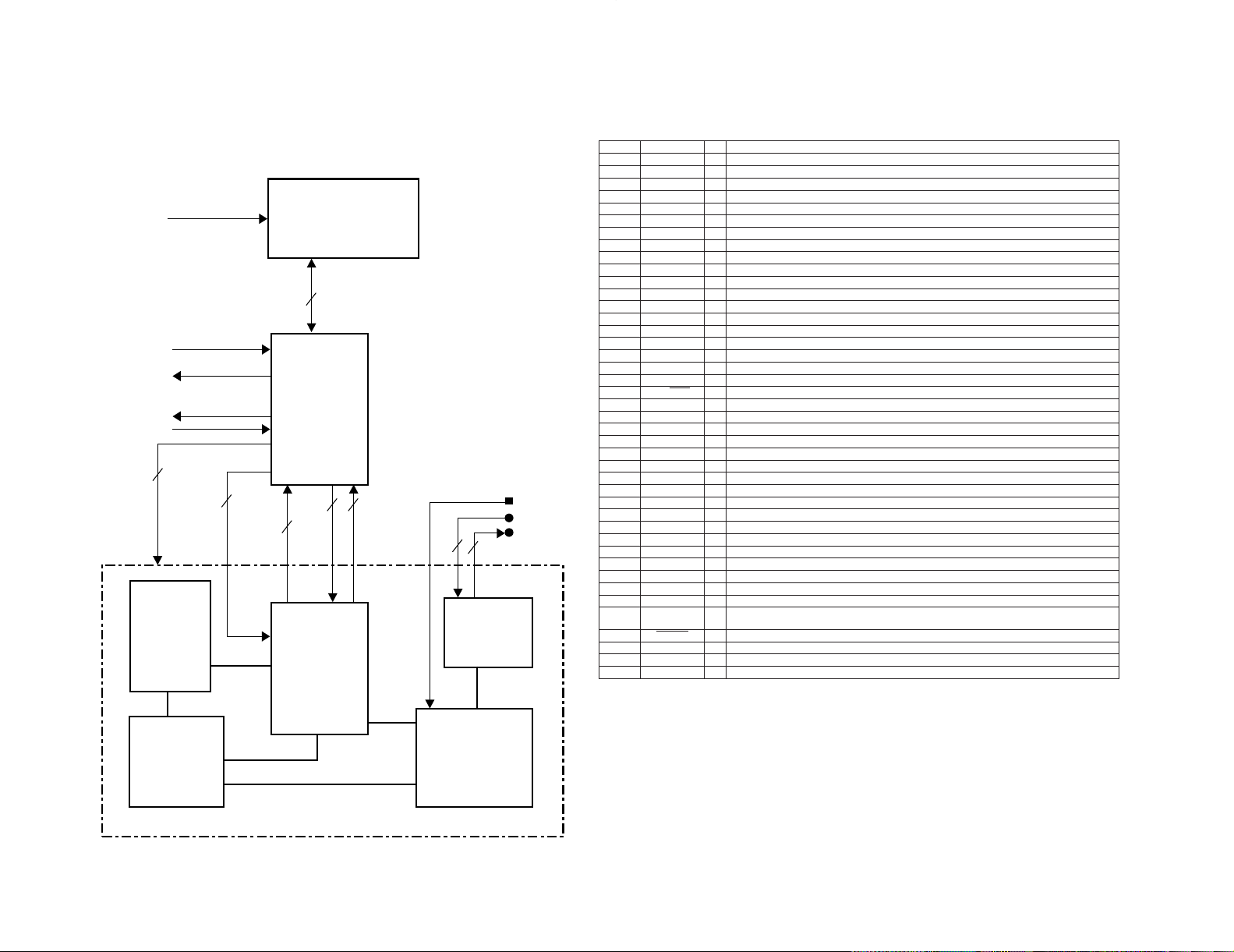
5. Composition (MD section)
5-1 Microprocessor periphery block diagram
Pin No Name I/O Description
1 PDOWN O MDM-98A POWER DOWN DETECTOR
2 SEARCH O CD SEARCH OUTPUT
3 LOAD IN I LOAD SWITCH INPUT
4 Avss – A/D POWER SUPPLY (CONNECTED TO GND)
5,6 – – NO USED
7 Avref1 – D/A REFERENCE VOLTAGE(+5V)
8 RXD I COMMUNICATION FROM MAIN u-COM (UART RXD)
9 TXD O COMMUNICATION TO MAIN u-COM (UART TXD)
10 – – NO USED
11 MD_DATA I MD IC IN DATA (MDM-98A IN DATA)
12 K_DATA O MD IC OUT DATA (MDM-98A OUT DATA)
13 DSCK O MD IC CK (MDM-98A CLOCK)
14 DSTB I MD IC STB (MDM-98A STB)
15 COMM_ANS I NO USED
16 COMM_DIN I NO USED
17 COMM_DOUT O NO USED
18 COMM_CLK I/O NO USED
19 COMM_REQ O NO USED
20~31 – – NO USED
32 6.5/5.0V O MD LOAD VOLTAGE CHANGE-OVER DISC LOAD/EJECT : H OTHER : L
33 Vss – u-COM(CONNECTED TO GND)
34~43 – – NO USED
44 INISW I INITIAL SW
45~58 – – NO USED
59 SRESET O NO USED
60 RESET I u-COM RESET
61 – I NO USED
62~66 – – NO USED
67 CE I u-COM CE
68 Vdd – u-COM POWER SUPPLY
69 X2 – 5MHz OSCILLATOR
70 X1 I 5MHz OSCILLATOR
71 IC – IC TERMINAL(CONNECTED TO GND)
72 NC – NO USED (OPEN)
73 GND I NO USED (CONNECTED TO GND)
74 Avdd – A/D POWER SUPPLY
75 Avref0 I A/D REFERENCE VOLTAGE
76 BACKUP I
BACKUP DETECTOR(A/D)
BACK UP : MORE THAN2.2V NO BACKUP:LESS THAN2.2V
77 AMUTE O ANALOG MUTE H : MUTE ON L : MUTE OFF
78 BACKUPSW O BACKUP DETECTOR SW H:ON(IN CASE of CE : HIGH) L:OFF(IN CASE of CE LOW)
79 MD_RESET O MD u-COM RESET H : NORMAL L : MD u-COM RESET (LOW EDGE)
80 MD_ST O MD ON/CD SYNC H : MD ON L : BACKUP MODE
5-2 Pin description of MD u-COM: uPD78058GC-B20 (X33 :IC1)
6. Test mode
6-1 Test mode of the receiver
(1) Setting of the test mode.
While pressing the [Band] key, plug the AC power cord into an AC power outlet.
(2) Canceling of the test mode.
Unplug an AC power cord.
(3) Condition in test mode.
POWER • • • • • • ON
SELECTOR • • • TUNER [BAND]
FL, LED • • • • • • All the fluorescent display indicate and LEDs light. (The all illuminated state is cleared by pressing any main
unit key or remocon key.
EX. BASS • • • • • OFF
7
CIRCUIT DESCRIPTION
RXD-M51/M51MD
8
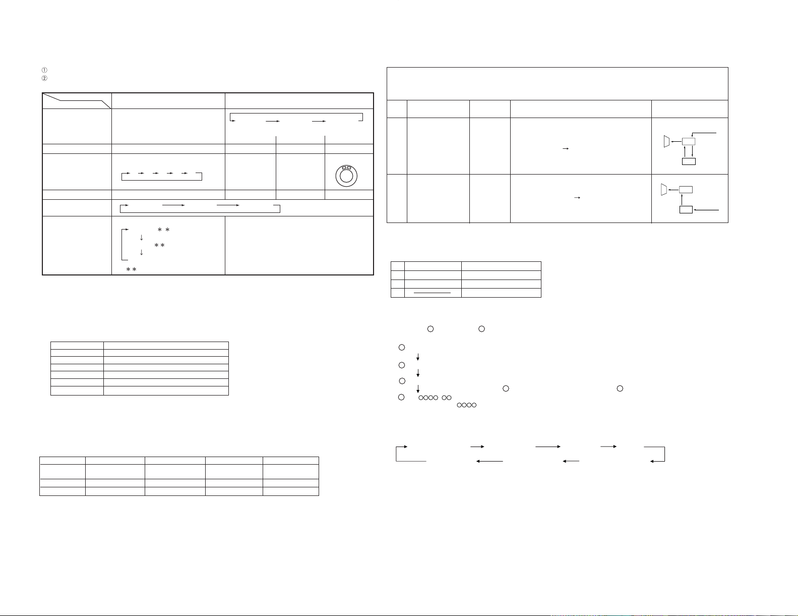
(4) Basic operation in test mode.
The muting during mode selection is not controlled in the test mode.
The test mode is cancelled when the AC power is turned OFF.
(5) The operation of the keys in the test mode.
6-2 Test mode of DECK section
(1) Setting
While pressing the TAPE key(DECK), plug the AC power cord into an AC power outlet.
(2) Resetting
Disconnect the AC power cord from an AC power outlet or press the [ON/STANDBY] key.
(3) Operation in TEST mode
(a) Initial condition
Item Condition
Power ON
Selector TAPE
Main VOL. 0dB (VOL. 80)
Input level(AUX) -6dB(INPUT 0)
EX. bass OFF
FL, LED, LCD All the FLs, LEDs, and LCDs are turned on
(b) 4-sec REC
• If the REC key is pushed, the system record for 4sec. Then, it rewinds to the REC starting position and plays back automatically.
• If the REC key is pushed during the 4-sec REC operation, the system records further for 4-sec, then returns to the starting position of the first 4-sec REC operation and plays back.
SERECTOR
TUNER AUX
OPERATION KEY
MENU
NORMAL ACTIVITY
DISPLAY DISPLAY DISPLAY
VOLUME INPUT BALANCE
(VOLUME15) (INPUT 0 ) (CENTER)
4 P.CALL : DOWN VOLUME 1 INPUT-6(dB) L ch MAX
7
P.CALL : 10 STEP CHANGEOVER
VOLUME 40 INPUT 0 (dB)
CENTER
10 20 30 40 01
¢ P.CALL : UP VOLUME 80 INPUT+3(dB) Rd MAX
REPEAT
EQU.MAX EQU.MINI EQU.FLAT
SOUND
S-LEVEL DISPLAY
(E.T only)
ATT OFF
ATT ON
NORMAL ACTIVITY
TUNER CATT OFF
: S-LEVEL A/D VALUE(HEX)
DOT (DISPLAY) 1st figure 2nd figure 3rd figure 4th figure
MECHA. HALF FWD REC INHIBIT RVS REC INHIBIT CRO2(TYPE¿) CASSETTE HALF
SWITCH DETECTION SW DETECTION SW DETECTION SW DETECTION SW
NG / / / /
OK T A P E
(c) Mechanism half switches indication
The mechanism half switches status are indicated "/ " or "TAPE" on the display as shown below.
6-3-1 Inspection mode
Setting : While pressing the [MD REC] Key, plug the AC power cord into an AC power outlet.
The "INSPECTION" shows on the display.
Cancellation : Unplug the AC power cord from an AC power outlet.
• The "DIGITAL1" is indicated on the display for a
second. "DIGITAL1"
CD input
• Source indicator (MD) is blinked.
• The "ANALOG" is indicated on the display for a
second.
• AUX input level
MID
• Source indicator (MD) is turned ON .
2 Digital through SOUND
test mode
1 Analog through SOUND
test mode
No.
Contents of
Keys Operation & Indication RemarKs
TEST mode
SEL.
MD
(PAUSE)
CD
DIGITAL
SP
SEL.
MD
(PAUSE)
AUX IN
(ANALOG)
REC IN
SP
6-3 Test mode of MD player
1. Preparation for adjustment
Test disc
6-3-2 MD TEST mode for adjustment
Type Test disc
1 High reflection disc TGYS1 (SONY)
2 Low reflection disc Recording minidisc
3 Head Adjusting transparent
2. Test mode
Test mode setting method
1. While pressing the [MD PLAY]key, plug the AC power cord into the AC power outlet.
(Start from A if no disc load, C if disc load.)
A MD
STEP Display
Change to step D if press <MD STOP> key. Return to C if press <MD REC>key.
: MD microprocessor version.
* Repair service is available for AUTO pre-adjustment and AUTO adjustment only.
Press MD STOP key to cancel the test mode if in needless test modes.
B EJECT
C AUT YOBI
Entering the specific mode
Whenever the [MD REC] button is pressed, the mode is changed.
AUTO pre-adjustment AUTO adjustment RESULT SUB RESULT
EEPROM setting MANUAL adjustment MANUAL pre-adjustment
(AUT YOBI) (AUTO AJST) (RST YOBI) (RESULT)
(EEPROM SET) (MNU AJST) (MNU YOBI)
D tsm e : Test mode STOP state
• Canceling the test mode
When the POWER button is pressed, the test mode is canceled, and the POWER OFF state is set.
( ): Display
RXD-M51/M51MD
CIRCUIT DESCRIPTION
2. AUTO adjustment mode
Step No.
Setting Method
Remarks Display
Step 1 Test mode STOP state [ t s m e ]
Step 2
Press the
MD REC button two times.
AUTO adjustment menu [ A U T O _ A J S T _ ]
Step 3 Press once the MD PLAY button. The slide moves to the innermost periphery, and automatic [ : _ _ _ _ _ _ ]
adjustment is started.
• In case of high reflection disc
changes as follows.
PEG→HAG
•In case of low reflection disc
changes as follows.
PEG→LAG→GCG→GEG→LAG
End of adjustment If adjustment is OK, Step 4.
If adjustment is NG, Step 7.
Step 4 Adjustment value output [ _ C O M P L E T E _ ]
Press the MD PLAY button. STEP 5
Press the MD STOP button. STEP 2
1. AUTO pre-adjustment mode (Low reflection disc only)
Step No.
Setting Method
Remarks Display
Step 1 Test mode STOP state [ t s m e ]
Step 2 Press once the MD REC button. AUTO pre-adjustment menu [ A U T O ]
Step 3 Press once the MD PLAY button. The slide moves to the innermost periphery, and automatic [ : _ _ _ _ _ _ ]
pre-adjustment is started.
• During automatic adjustment
changes as follows.
HAo→RFg→SAg→SBg→PTG→PCH→GTG→GCH→RCG→
SEG→RFG→SAG→HAO→HEO→TCO→LAO
End of adjustment If adjustment is OK, Step 4.
If adjustment is NG, Step 5.
Step 4 Grating adjustment, [ _ C O M P L E T E _ ]
adjustment value output
Press once the MD STOP button. STEP 2
Step 5 Adjustment value output [ A U T Y O B I ]
Press once the MD STOP button. STEP 2 AUTO pre-adjustment menu
• : Adjustment name, : Address
• Test Mode
1. AUTO pre-adjustment mode • Automatic pre-adjustment is performed. (After adjustment the grating adjustment mode is set.)
• The adjustment value is output with the aid of system controller interface.
2. AUTO adjustment mode • Automatic adjustment is performed.
• The adjustment value is output with the aid of system controller interface.
• Continuous playback is performed. (Error rate indication, jump test)
3. RESULT sub-mode* • The measurement value, set value and calculated value are indicated.
• The set value is changed manually (in servo OFF state).
4. RESULT mode (final adjustment)* • The set value (after calculation) is indicated.
• The set value is changed manually (in servo OFF state).
5. MANUAL pre-adjustment mode* • RF side manual adjustment is performed.
• Focus and tracking signal ATT manual adjustment is performed.
• Focus and tracking signal offset setting is performed.
6. MANUAL adjustment mode* • Focus
• Don't adjust.
and tracking signal ATT manual adjustment is performed.
7. EEPROM setting mode*
8. TEST-PLAY mode* • Continuous playback from the specified address is performed.
• C1 error rate measurement,
*
This mode is not used for service.
9. TEST-REC mode* • Continuous recording from the specified address is performed.
• Change of record laser output (servo gain is also changed according to laser output)
10. EJECT mode* • TEMP setting (of EEPROM setting)
Step 5
Continuous playback (groove section)
[ a c ]
Step 6 Press the MD STOP button. STEP 2 AUTO adjustment menu
Step 7 Adjustment value output [ C a n ' t _ A D J . ]
Press the MD STOP button. STEP 2 AUTO adjustment menu
• : Adjustment name, : Measurement value, : Address
Step No.
Setting Method
Remarks Display
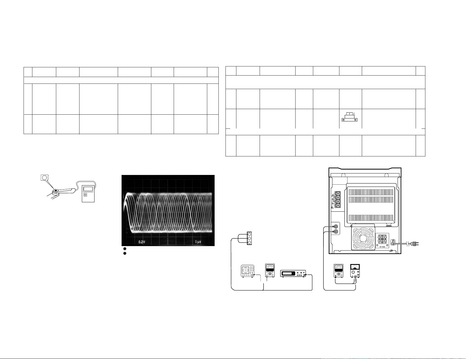
Figure 1-1 Optical Pickup Grating Deviation
Measuring Method
Mechanism Adjustment
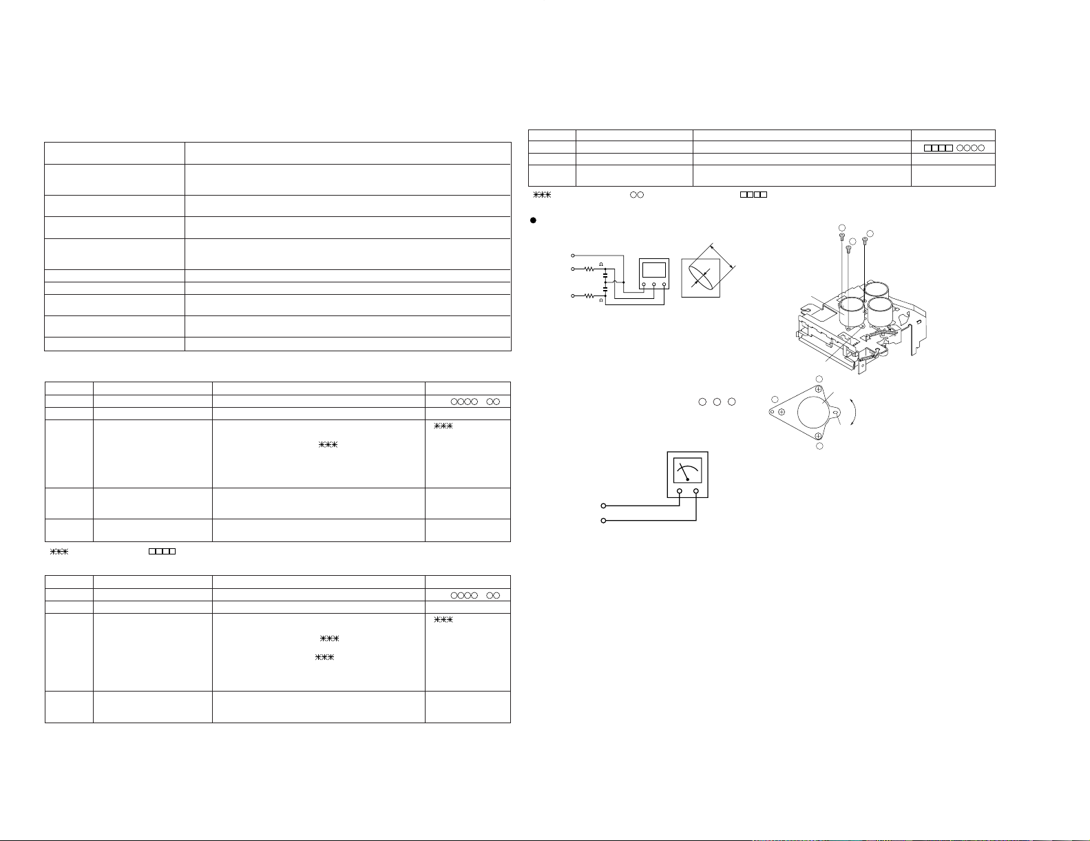
1. Optical pickup grating inspecting method
After the automatic adjustment is performed in the AUTO
mode (test mode) with the aid of high refection MD disc
("COMPLATE" is displayed), the Lissajous's waveform (x-y) is
adjusted.
1. Slightly loosen the 3 screws of spindle moto, and maken an
adjustment, observing the Lissajous's waveform.
2. After adjustment tighten the screw in arder of 1 , 2 , 3 .
Figure 1-2
2. Jitter adjustment and checking method
Figure 1-3 Jitter connection diagram
After performing automatic adjustment in AUTO mode of
TEST mode using the low reflection MD disc, check this jitter
in pit continuous playback and groove continuous playback
mode.
9
43 pin of IC 1101
GND
26 pin of IC 1101
EOUT
25 pin of IC 1101
FOUT
100K
100K
3pin of IC 1201 (TP1274)
EFMMON
13 pin of IC 1201 (TP1275)
GND
1
3
3
Spindle motor
adjusting
hole
2
2
Check the Lissajou's waveform,
shifting the mounting position with
a screwdriver (to be fitted into the
disc motor adjusting hole).
CIRCUIT DESCRIPTION
OSILLOSCOPE
470p
470p
GND CH1 CH2
XY
LISSAJOUS'S WAVEFORM
Less thana:b = 3:1
a
b
Spindle Motor
Adjusting hole
1
jitter Meter
RXD-M51/M51MD
10
6-4 Test mode of CD player
6-4-1 Main unit
(1) Setting of the test mode
While pressing the [CD PLAY] key, plug the AC
power cord into an AC outlet.
(2) Canceling of the test mode.
Unplug the AC power cord from AC power outlet or
press the [SET] key.
(3) Operation
6-4-2 Mecha. manual mode
(1) Setting
While pressing the [DISC 1 PLAY] Key, plug the AC
power cord into an AC outlet.
(2) Cancelling
Press the [ON/STAND BY] Key.
(3) Operation
KEYS INDICATION OPERATION
FF CD MANUAL LIFT MOTOR UP
FB CD MANUAL LIFT MOTOR DOWN
DISC 2 CD MANUAL LOAD MOTOR OPEN
DISC 3 CD MANUAL LOAD MOTOR CLOSE
KEY
[DISC3 PLAY]
+AC
CD 5 01
POWER ON, SEL CD
Mecha. initialization
Tray 3 opens
STOP CD 5 01 STOP
FF
CD 5 01
Pick manual feed (INîOUT)
(Stop mode only)
FB
CD 5 01
Pick manual feed (OUTîIN)
(Stop mode only)
SKIP DOWN
SKIP UP
CD 5
CD 5 06
Indication
: Adjustment value/Mean
value (stop mode only)/HEX
Read TOC î play
DOT TNO SEC.
section section section
TB/FB TB value FB value
TG/FG TG value FG value
FE/RF FE value RF value
TE/VC TE value VC value
PLAY/PAUSE
PAUSE
óï
PLAY
(Cyclically
changed)
CD 5 05
PLAY MARK
ON ‰
CD 5 03
PAUSE MARK
ON 8
TRAY CLOSE/DISC CLAMP
03 MODE
(TRACKING SERVO OFF)
05 MODE
DISPLAY OPERATION
DISPLAY DESCRIPTION
BLANK DISC Non Recorded disc
CAN'T COPY Inhibit to record by SCMS
CAN'T EDIT Inhibit to edit by MD standard
CAN'T REC Inhibit to record by disc damage(10 or more
defects/recordable cluster is 0)
DISC ERROR** OR : UTOC read error or FTNO>LTNO
(edit/record) permit ALL ERASE only
DO : Start address TNO>endless TNO
(playback) handle poor TNO as 1SG
(edit/record) permit ALL ERASE only
C0 : Write poor data in UTOC0
C1 : Write poor data in UTOC1
C2 : Write poor data in UTOC2
C4 : Write poor data in UTOC4
(play back) playback even if address
roof(C0)
(edit/record) permit ALL ERASE only
DISC FULL No recordable area
MECH ERR** 10-13 : head poor down
20-23 : head poor up
no disc No disc in the unit
NO TRACKS Disc recorded title only
NOT AUDIO Disc recorded audio signal.
PLAY ONLY Record to music disc
PROTECTED Record disc inhibited to record
READING In mode of reading TOC or UTOC
SRCH ERR** 30 : Search time over in playback, FF or FB
31 : Search time over in REC-PAUSE
32 : Search time over in record
TEMP OVER High temperature
TITLE FULL Input over letter of title
UNIT ERROR Hardware damage
UTOC W ERR Error of writing to UTOC
WRITING In writing to UTOC
7. MD mechanism error message
RXD-M51/M51MD
CIRCUIT DESCRIPTION
(b)
(a) Laser Power
Pickup
0.05~0.15 mW
Optical power meter
RF signal in test mode (PLAY).
Perform the tangential and focusing offset are focused
into one point on the display. The crossing points above
and below the center shall also be looked clearly.
No.
1
2
ITEM
LASER
POWER
FOCUS
ERROR
BIAS
INPUT
SETTING
–
Test disc
Type 4
OUTPUT
SETTING
Connect an oscilloscope
as follows.
(+)side : RF(CN1-1)
GND : VC (CN1, 4)
Set the senor section of
the optical power meter
on the pickup lens.
PLAYER
SETTING
Press the "PLAY"
key to check that the
display is "03".
Press the "PLAY"
key. Confirm that
the display is "05".
ALIGNMENT
POINT
VR1
–
ALIGN FOR
On the power
from.0.05 to
0.15mw. when the
diffraction grating is
correctly aligned
with the RF level of
0.8Vp-p or more
Optimum eye pattern
FIG.
(a)
(b)
Note:
Type 4disc :SONY YEDS-18 Test Disc or equivalent.
LPF : Around 47kΩ + 390pF or so.
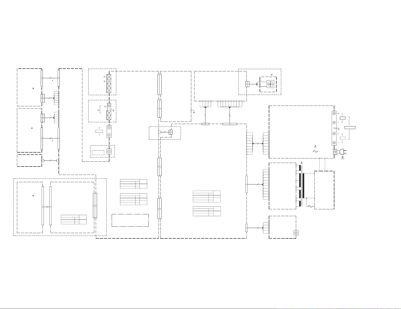
Adjustment of CD player
TEST MODE : While pressing the [DISC 3 PLAY] key, plug the AC power cord into the AC outlet.
RF signal : AC coupled
★ The MD Adjustment is listed on page 8 through p10.
AG
{
(A)
(B)
Oscilloscope
AC voltmeter AC voltmeter
Frequency counter
X09 CN3
TEST PIN
1
2
3
PLAY (L)
GND
PLAY (R)
RVS FWD
NO. ITEM
INPUT
SETTING
OUTPUT
SETTING
CASSETTE TAPE
DECK SETTING
ALIGNMENT
POINTS
ALIGN FOR FIG.
Unless otherwise specified, set the respective switches as follows: 0dBs = 0.775V
TAPE : NORMAL DOLBY : OFF
I Cassette mechanism unit (Adjustment of the REC / PLAY head)
(1)
Demagnetization
and cleaning
——
Power : OFF
Demagnetization,
cleaning, PLAY
Recording
head, erase
head, capstan
pinch roller
Demagnetize the REC / PLAY head
with the head eraser. Clean the REC/
PLAY head, erase head, capstan and
pinch roller using a cotton swab slightly
damped with alcohol.
(2)
Azimuth of the
REC / PLAY
head
SCC-1727
TCC-153
MTT-114
10kHz, -10dB
(B) PLAY
Adjust the output to maximum and
adjust the azimuth adjustment screw
for the Lissajours waveform pattern of
the oscilloscope to become close to a
45˚ straight ling.
II PC board adjustment.
(1)
BIAS
CURRENT
(A)
Adjust the AG for the
output of the DECK to
become 12.5KHz –20dBs.
400Hz / 12.5kHz
(AC-224)
(B) REC PLAY
VR3(L)
VR4(R)
Record 400Hz and 12.5kHz alternately,
and adjust the bias current adjustment
potentiometer for the playback levels to
become the same.
ADJUSTMENT
11
RXD-M51/M51MD
12
CN4
CN1501
CN2 CN205
CN2
WH1
WH202
CN202
WH201
GND
FM 300
AM ANT
FM 75
AM ANT
FM
300
GND
FM
75
Lch 1
Rch 2
AUX IN
J1
J201
J201
A201
CN206 CN1
CN207 CN2
WH203 CN11
CN4 CN1
CN1 CN2
E4
E6
E1
E5
WH4WH3
WH1
R-ch
L-ch
1
2
J1
CN6
CN4
CN7 CN8
SPEAKERS
E3
CN3
CN5
WH1
E1
J1
HEADPHONE
RXD-M51 (X07-299X-XX)
RXD-M51MD (X07-2992-71)
RXD-M51 (X09-612X-XX)
RXD-M51MD (X09-6122-71)
RXD-M51MD (X33-1172-71)
DIGITAL OUT
(OPTICAL)
A301
WH2
FAN
28
28
28
1
1
18
1
1
12
12
1
12
E35-2015- 5
7
1
7
1
6
16
1
5E35-2200-
6
16
16
1
2
18
1
12 12
11
10 10
11
2
1
1
2
12 12
11
10 10
11
2
9
1
10
1
1
12
(M)
(T,E)
: AC110-120V/220-240V~
50/60Hz
: AC230V~ 50Hz
WH6
WH5
BRN
YEL
15
1
2
2
1
15 1 10
1
9
12
1
12
10
5
F1
2
1
5
5
1
5
1
DESTINATION
ABB.
COUNTRY
EUROPE
U.K.ET
UNIT No.
2-71
GENERAL MARKET
ABB.
EUROPE
U.K.ET
COUNTRY
DESTINATION
M
2-72
UNIT No.
0-21
EUROPE
U.K.
DESTINATION
GENERAL MARKET
COUNTRY
E
T
M
2-72
0-21
ABB.
UNIT No.
EUROPE
DESTINATION
U.K.
COUNTRY
E
T
2-71
ABB.
UNIT No.
EUROPE
U.K.
COUNTRY
E
T
ABB.
2-71
DESTINATION
UNIT No.
7
1
6
1
2
1
2
1
P1
9
(D40-1602-
MD MECHANISM
5)
(X33-117X-XX)
USED RXD-SE5MD/RXD-M51MD
MECHANISM
(D40-1601- 5)
CASSETTE
(D40-1612-
CD MECHANISM
5)
(X09- ) (B/2)
USED (T,E)TYPE
USED (M)TYPE
(A/2)
USED
RXD-M51
(X07-299X-XX) (A/5)
(X07- ) (B/5)
(X07- ) (D/5)
(X07- ) (E/5)
(F09-0140-
FAN
PRIMARY UNIT
SECONDARY UNIT
(X07- ) (C/5)
(X14- ) (B/2)
HEADPHONE
RXD-M51
MD UNIT
(X09-612X-XX)
AUDIO UNIT
RXD-M51(T,E)/RXD-M51MD(T,E)
RXD-M51(M)
TUNER PACK
: W02-2666-05
: W02-2667-05
RXD-M51MD
RXD-SE5MD/
USED
(X14-4870-00)
DISPLAY UNIT
(A/2)
5)
RXD-M51MD
USED
POWER AMPLIFIER UNIT
RXD-M51MD
MDM-98A
RXD-M51/M51MD
WIRING DIAGRAM
ACEBD
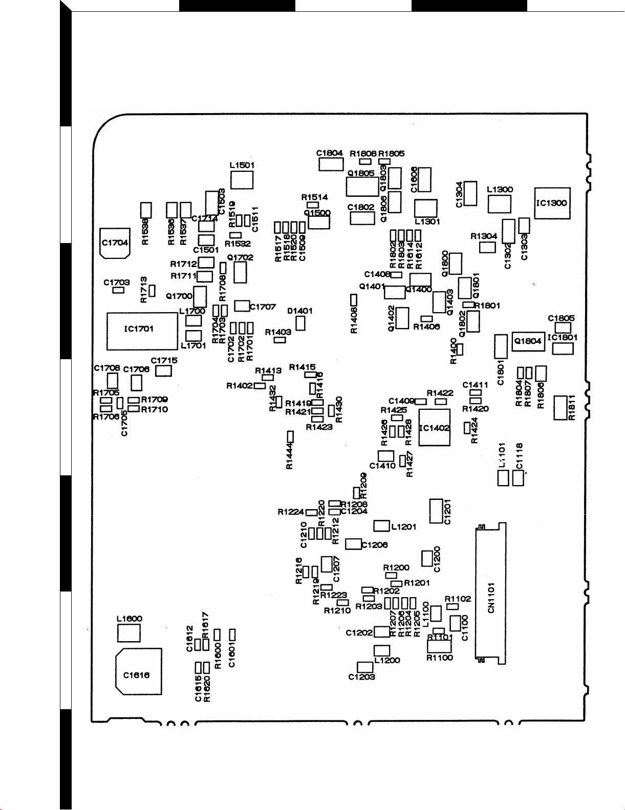
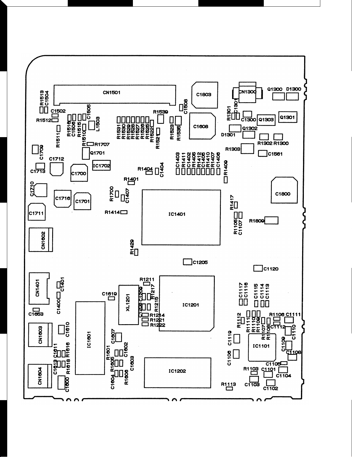
PC BOARD PARTS LOCATION
1
2
3
4
5
6
7
Refer to the schematic diagram for the value of resistors and capacitors.
MD MAIN PWD-A (TOP VIEW)
13
F GIHJ
PC BOARD PARTS LOCATION
1
2
3
4
5
6
MD MAIN PWB-A (BOTTOM VIEW)
7
14
 Loading...