Kenwood RX-DM505-USBB, LSM-505-S, LS-M505-B Service Manual
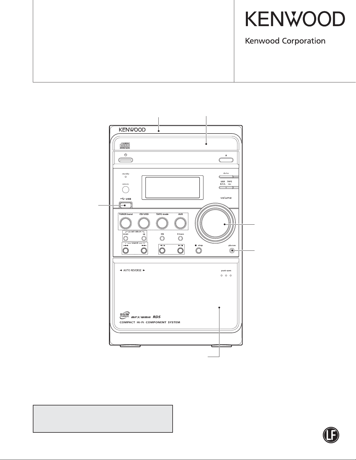
COMPACT Hi-Fi COMPONENT SYSTEM
RXD-M505USB-B/M505USB-S
LS-M505-B/M505-S
SERVICE MANUAL
(M-505USB)
Front cabinet
(A60-2529-08) : S
(A60-2532-08) : B
USB jack
(E58-0096-08)
© 2007-10 PRINTED IN JA PA N
B53-4023-00 (N/J) 122
CD door
(A29-1280-08) : S
(A29-1284-08) : B
Volume knob
(K29-8628-08) : S
(K29-8643-08) : B
DANGER:
Please do not look at the laser beam directly during
re pair or operation check.
Cassette door
(A53-2490-08) : S
(A53-2492-08) : B
S : Silver
B : Black
This product complies with the
Phones jack
(E11-1012-08)
This product uses Lead Free solder.
RoHS directive for the European market.
RXD-M505USB/LS-M505
ACCESSORIES / CAUTIONS
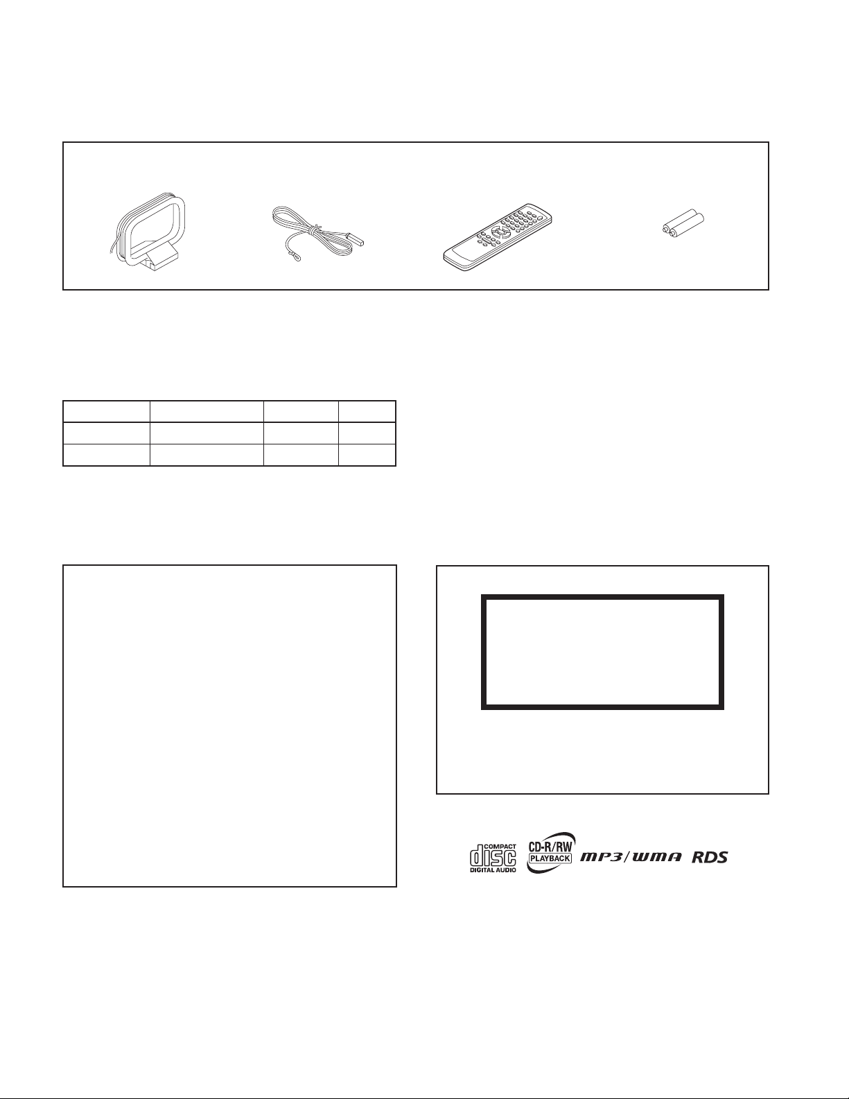
Accessories
AM loop antenna (1)
(T90-0926-08)
FM ANT Wire (1)
(T90-0925-08)
SYSTEM vs COLOR
SYSTEM RECEIVER SPEAKER COLOR
M-505USB-B RXD-M505USB-B LS-M505-B BLACK
M-505USB-S RXD-M505USB-S LS-M505-S SILVER
Cautions
Remote control unit (1)
RC-F0320E
(A70-1727-08)
Batteries (R6/AA) (2)
(–)
Resetting the Microcomputer
The microcomputer may malfunction (unit cannot be
operated, or shows an erroneous display) if the power
cord is unplugged while the power is ON, or due to
some other external factor. If this happens, execute the
following procedure to reset the microcomputer and
return the unit to its normal operating condition.
When the power is on and TUNER input is
selected, press and hold down the (■ stop)
button on the unit for more than 2 seconds.
Unplug the AC cord and plug it back in if “INIT.
OK” is appears.
• Please note that resetting the microcomputer will
clear the contents of the memory and return the unit to
the state it was in when it left the factory.
The marking of products using lasers
CLASS 1 LASER PRODUCT
LASER KLASSE 1
APPAREIL A LASER DE CLASSE 1
LUOKAN 1 LASERLAITE
KLASS 1 LASERAPPARAT
The marking this product has been classifi ed as Class 1.
It means that there is no danger of hazardous radiation
outside the product.
Location: Bottom
2
RXD-M505USB/LS-M505
EXTERNAL VIEW
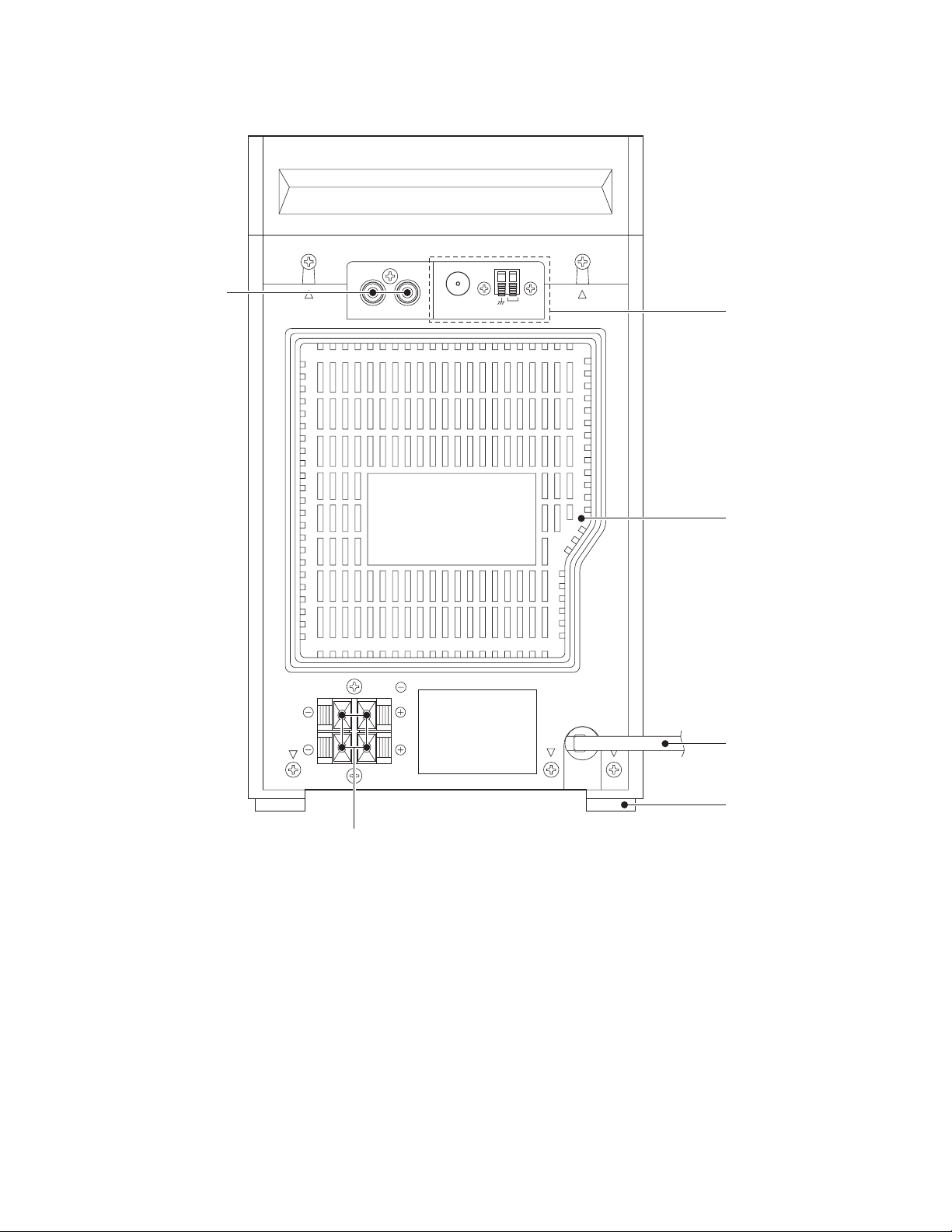
RCA jack
(E63-1426-08)
SPEAKER
IMPEDANCE
47
RL
AUX IN
L
R
FM ANT.
757
L
R
AM ANT.
Tuner module
(W02-4673-08)
Rear cabinet
(A80-4576-08) : S
(A80-4577-08) : B
AC Cord*
(E30-)
Speaker terminal
(E70-1034-08)
Rubber foot
(J02-1590-08)
* Refer to parts list on page 20.
3
RXD-M505USB/LS-M505
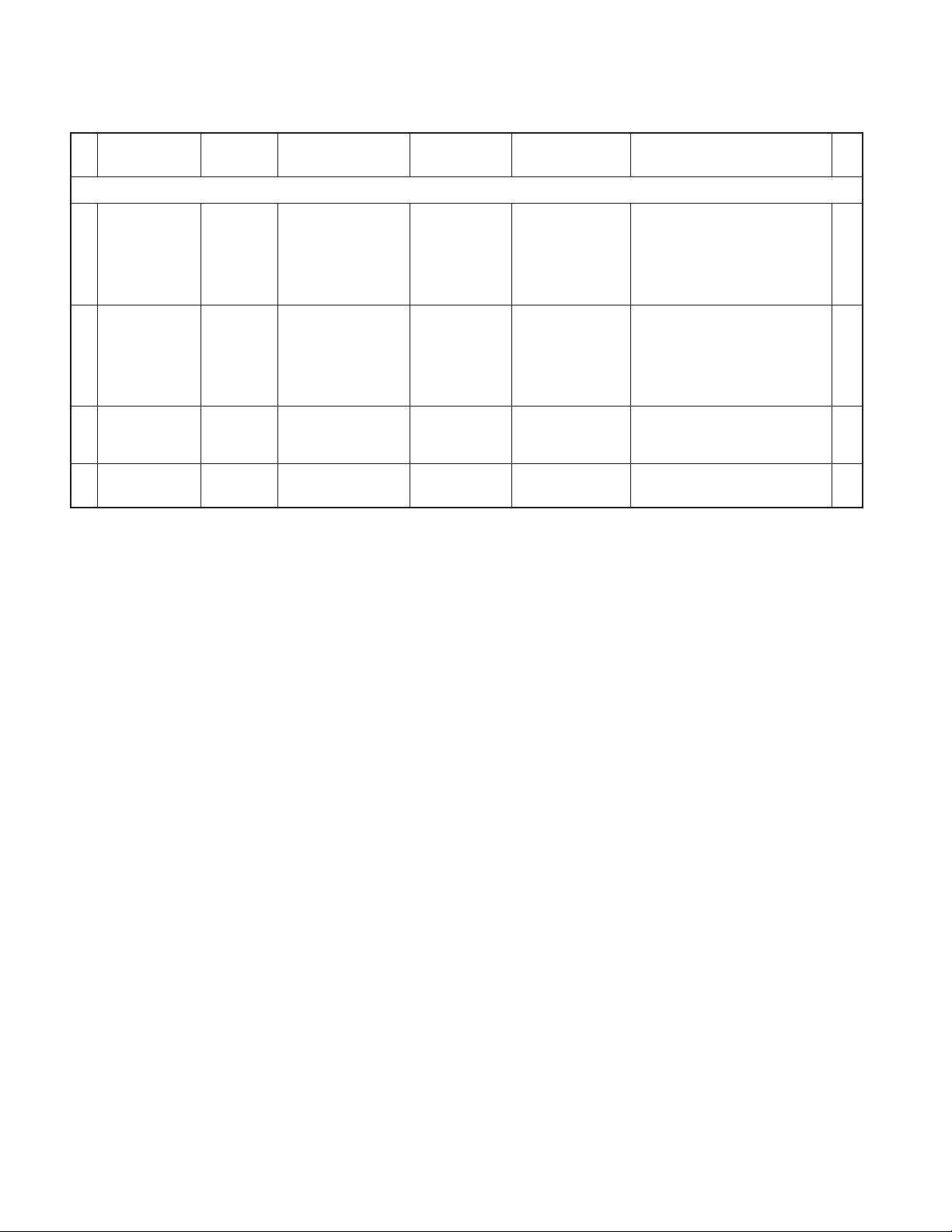
ADJUSTMENT
No ITEM
Demagnetization
1
and cleaning
2 Azimuth of Heads
3 Tape Speed
4 Bias Frequency Normal tape
INPUT
SETTING
--
MTT-114:
10kHz,-10dB
MTT-111
3kHz
OUTPUT
SETTING
Connect the
oscilloscope and VOM
to PHONE jack.
Connect the
oscilloscope and VOM
to PHONE jack.
Connect the frequency
counter across C202
RECEIVER
SETTING
ALIGNMENT POINT ALIGNMENT SETTING FIG.
Cassette deck
Power: OFF
Demagnetization
and cleaning
PLAYBACK Screw fi xing heads
PLAYBACK
RECORD L203
Heads, capstan and
pinch roller
Potentiometer in
motor
Demagnetize heads with the head
eraser (Demagnetizer). Clean
heads capstan and pinch roller
using a cotton swab slightly
damped with alcohol
Adjust the output to maximum and
turn the azimuth adjusting screw
for Lissajours waveform pattern of
the oscilloscope to become close
to a 45-degrees straight line.
Adjust the tape speed so that 3kHz
is obtained at the center of tape.
The frequency counter shows
85kHz+-0.5kHz
4
EDCBA
RXD-M505USB/LS-M505
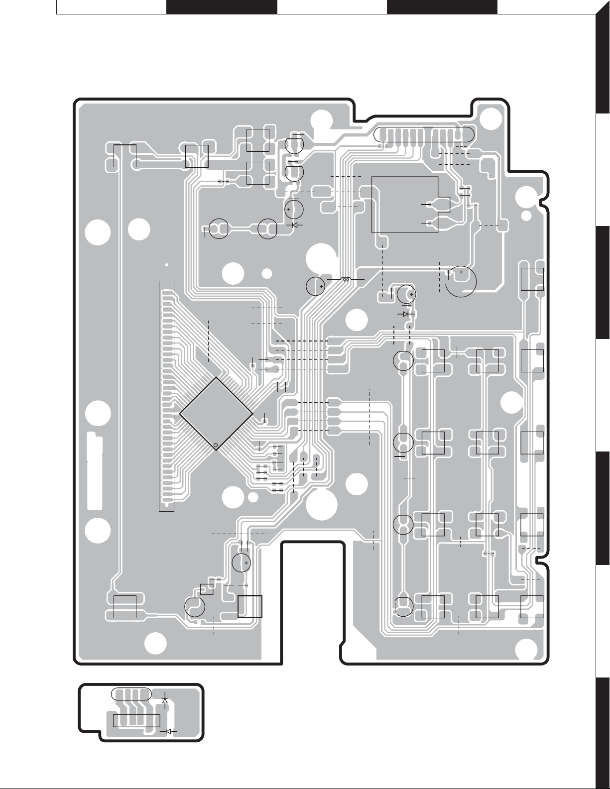
PC BOARD
DISPLAY
SW501
OPEN
381
LCD501
SW502
16 17
R516
J534
DEMO
J541
32
IC501
1
LED502
33
64
SW504 SW503
LED501
C516
C517
C522
48
49
R538
R520
R519
J533
J532
C509
TAPE REC
USB O.T.E
C521
C520
C515
C514
C513
C512
C511
R507
C510
R518
R517
R509
BCE
R511
R510
BCE
R513
J535
D502
C508
J531
J530
J529
J528
J527
J526
J525
J524
J522
J521
Q502
Q503
J523
J537
J536
J538
L501
12 1
R512
CN1
C502
C501
C518
C519
J502
J509
D503
J511
J510
SW506SW505SW507SW511
LED503
J519
LED504LED505
R515
J545
J508
J504
J505
C504
C503
R502
R501
VR501
J512
J503
J506
C532
J507
SW508SW512SW516SW513
EQ X.BASS
STOP
SW712
SW514SW518SW509SW517
RPLAY/PAUSE
1
2
3
FPLAY/PAUSE
4
USB
CN502
SW515
STANDBY
14
14
D509
C530
D508
LED507
R506
Q501
R508
BE
J542
C505
J520
C507
C506
GOI
R504
R503
SENSOR
IC502
SEARCH +
J518
J513
J514
ALBUM UP
J516
J515
LED506
R514
TUNER/BAND CD/USB TAPE MODE AUX
J517
ALBUM DOWN
SEARCH -
Refer to the schematic diagram for the values of resistors and capacitors.
5
6
7
5
F G H I J
RXD-M505USB/LS-M505
1
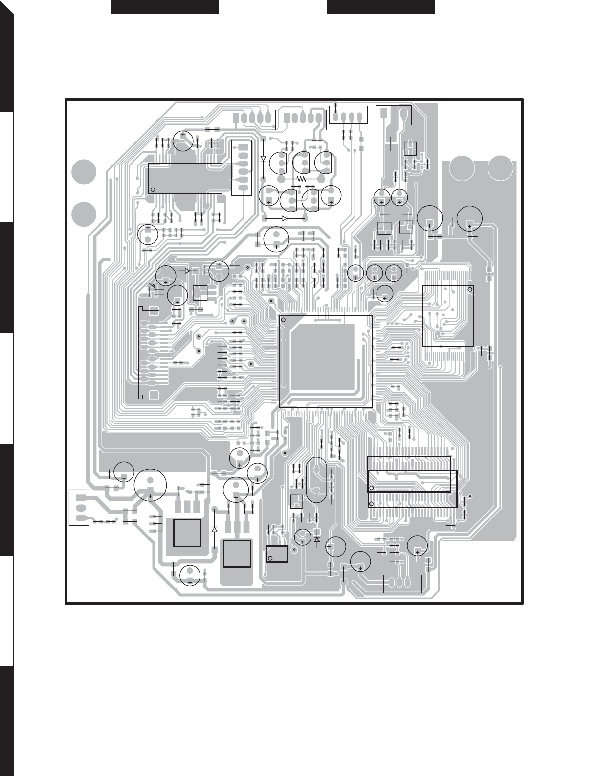
PC BOARD
CD (SIDE A)
CN12CN3
141
R47
R48
EC3
U9
R59
D2
EC16
R16
U1
L21
BC50
BC8
TP9 TP10
BC16
GIO
Q3
R15
R5
BC49
R28
C26
C28
C30
C32
R31
R64
C45
C33
C34
R56
R53
EC15
BE
BC26
C35 R34
C36 R35
L4
D1
BC10
15
14
R52
C21
C22
C23
C24
EC12
R55
R37
EC1
BC20
BC24
C20
TP7
C29
C31
16
CN11
R29
BC7
R30
C25
C27
BC28
R32
R33
R18
GOI
U2
TP6
TP8
BC27
BC30
BC31
BC1
R19
D4
EC22
D5
L14
C17
C19
TP11
BC18
C11
C15
BC43
C18
L22
8
1
R69
R26
TP5
R40
EC11
R49
Q9
BCE
R66
Q5
C12
BC29
154
TP12
U6
R67
EC4
R25
BC41
216
55
BC37
Q4
R50
5
4
R70
BCE
C14
R41
EC18
R22
R21
R74
R72
BE
C46
R68
BCE
BC11
C7
C9
C10
R73
C40
TP13
Q7
R23
R71
R46
EC5
R58
C44
BC48
EC17
BC23
R63
R2
28
1
R54
EC14
BC6
CN7
C42
BC25
R61
R57
161
R62
C43
BC21
BC22
R20
R60
2
3
4
EC20
EC2
BC51
L7
5
13
L2
BC12
L3
R6
CN4
BC4
BC5
BC3
BC17
L13
5
R65
BCE
Q6
C8 BC42
C13
R24
XT1
R43
D3
BCE
R1
BC40
BC2
U3
BC13
R7
14
CN2
R76
R77
L5
Q8
EC21
R75
C48
BC53
C50
C49 C47
EC31
BC9R3
R17 BC19
C37
R42
C38
EC7
L16
F1
EC6
13
EC27
C63
Q17
R93
R95
R96
EC23
C16
163
162
BC32
BC36
109
C41
108
BC35
50
54
1
1
R13
R12
CN6
CN13
Q20
C65
Q21
R82
EC13
BC39
BE
R84 R81
BE
EC25
BC45
EC29
R80
BC14
R4
C64
R78
R79
24
25
L6
R8
BE
R83
BC38
R51
BC46
U8
U7
R10
R11
14
EC19
C5
C6
R9
R14
L19A
EC8
U11
26
25
BC47
BC33
28
27
BC34
R45
R44
1
48
TP14
EC10
L20
BC44
L8
6
7
Refer to the schematic diagram for the values of resistors and capacitors.
6
ONMLK
RXD-M505USB/LS-M505
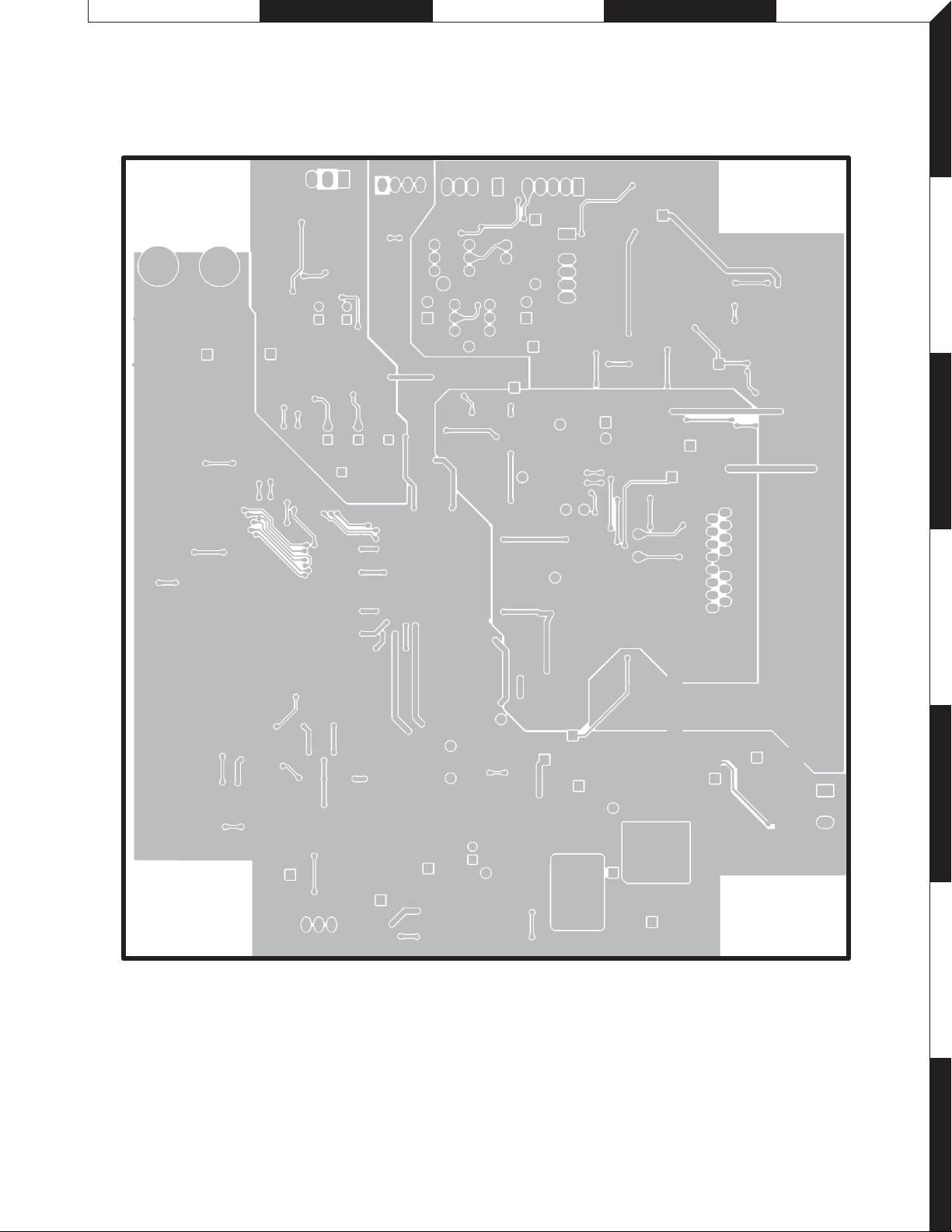
PC BOARD
CD (SIDE B)
1
2
3
4
5
6
Refer to the schematic diagram for the values of resistors and capacitors.
7
7
P Q R S T
7
0
3
R
J305
5
R
5
5
RXD-M505USB/LS-M505
1
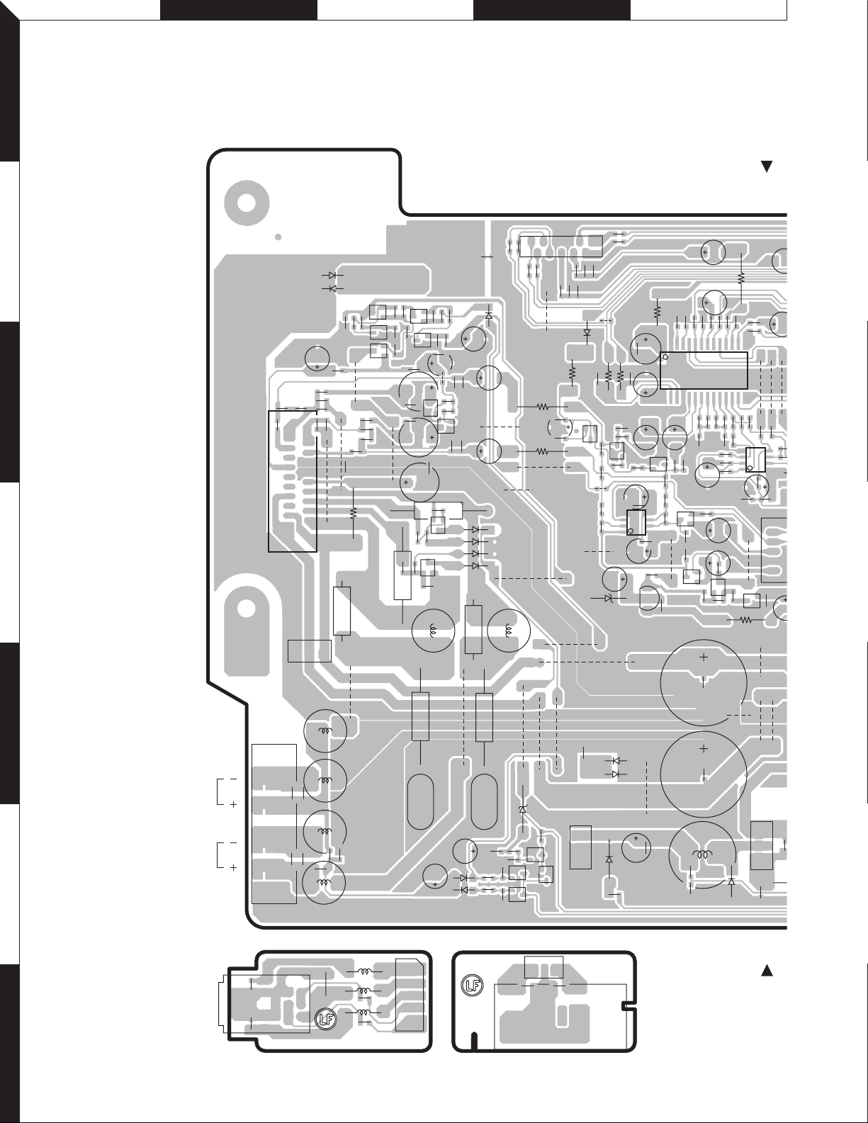
PC BOARD
MAIN
2
D107
C427
L206
L207
L208
L209
R283
102
R282
D108
Q418
C417
R411
Q431
R486
R485
CN103
BE
R413
R412
R414
BEBE
Q419
C419
R405
R401
J433
3
C403
L410
IC402
19 1
R403
C405
R407
C406
18 2
J416
R408
J417
L408
C426
R406
R402
R404
C404
Q420
C416
R415
C401
C438
J432
4
R421
R410
CN406
J411
L409
5
CN401
L404
L
R
6
R434
C453
C451
R429
R479
L405
R478
R477
L407
PHONE
L414
L413
C421
JK400
C422
7
L436
L412
R483
R484
CN403
R503
BE
C464
BE
R489
R497
R469
Q430
R417
R463
C439
R422
Q406
R423
C424
R425
C425
R424
L402
R462
C429
C436
BE
C420
BE
BE
R460
R461
C409
R420
Q404
J434
BE
C402
C470
Q405
R419
Q403
C437
D401
C412
J410
R418
C413
C488
C489
R409
R472
R476
D402
AUX
51
J435
D403
D404
D405
D406
R464
C465
R470
CN302A
D412
L401
R471
R473
R455
R456
J431
Q411
R366
J428
J426
ZD406
BEBE
C333
R365
C340
J321
J407
BE
Q410
3
J301
R474
Q414
BE
JK302
R371
R310
J425
1
C334
R281
R372
J427
CN404
Q415
R280
ZD410
J406
C191
J104
D301
Q303
C480
31
111
BE
C190
C477
J429
J105
R499
C442
R494R495
R330
R370
IC401
C431
D410
D411
D413
R498
L210
L211
R331
R367
R340
BE
R369
C440
R491
148
C450
C301
R353
C368
R314
C320
C309
C317
C318
114
C319
C308
R343
R302
R357
C307
R344
R301
IC301
28 15
C479
C328
C325
C326
Q302
R440
C441
EBC
Q401
R496
J424
C452
Q301
5
BE
C460
R445
R448
J318
C445
Q425
R481
R341
C462
C443
Q426
R439
R441
R368
BE
C444
C324
R316
C338
R475
BE
C418
C448
C322
R361
R468
C449
L403
C323
R459
C321
R315
R363
R362
BE
R490
C312
R312
C327
C463
R480
Q428
J450
C310
C316
IC403
148
R360
J430
R458
Q427
D408
C3
C36
J302
J303
J304
C311
C315
R3
5
R3
C
R482
R359
CN402
15
BE
R454
J403
J404
J405
E
R437
B
C4
Q412
C423
8
 Loading...