

Page 1
70%
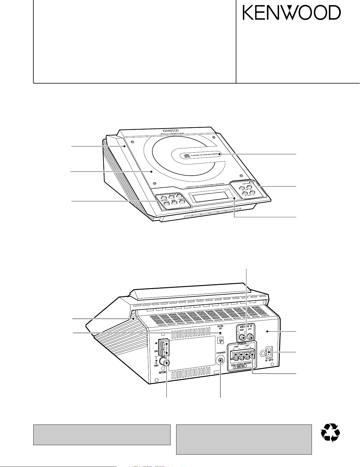
COMPACT AUDIO SYSTEM
RD-M23
SERVICE MANUAL
(For M,X type)
Front cabinet
(A60-2147-08)
CD lid
(J19-6268-08)
Knob
(K29-8084-08)
© 2001-9 PRINTED IN KOREA
B51-5756-00 (K/K) 547
Plate
(B03-3900-08)
Knob
(K29-8085-08)
Clear panel(DISK)
(B10-3764-08)
Bottom cabinet
(A10-3564-08)
Digital out jack
(W02-2878-08)
Terminal
(E70-0149-08)
In compliance with Federal Regulations, following are reproduction of labels on, or inside the product relating to laser product safety.
Socket
(E63-1228-08)
Rear panel
(A80-4203-08)
Socket
(E03-0384-08)
Terminal
(E21-0040-08)
Headphone jack
(E11-0944-08)
KENWOOD-Corp. certifies this equipment conforms to DHHS
Regulations No.21 CFR 1040. 10, Chapter 1, subchapter J.
DANGER : Laser radiation when open and interlock defeated.
AVOID DIRECT EXPOSURE TO BEAM.
Page 2

AC power lead x1
(E30-7240-08): X
(E30-7237-08): M
Remote control x1
(A70-1547-08)
Battery cover(A09-1243-08)
FM antenna x1
(T90-0891-08)
AM loop antenna x1
(T90-0890-08)
"AAA" size battery
(UM-4, R03, HP-16 or similar)x2
RD-M23
Troubleshooting
If trouble occurs
When this product is subjected to strong external interference
(mechanical shock, excessive static electricity, abnormal supply
voltage due to lightning, etc.) or if it is operated incorrectly, it may
malfunction.
If such a problem occurs, do the following:
Caution:
This operation will erase all data stored in memory including clock,
timer settings, tuner preset, and CD programme.
1 Set the unit to the stand-by mode and turn the power on
again.
2 If the unit is not restored in step 1, unplug and plug in the
unit, and then turn the power on.
3 If neither step 1 nor 2 restores the unit, do the following:
Press the ON/STAND-BY button to enter the power stand-by
mode.
Unplug the AC power lead from the AC INPUT socket on the
unit.
Whilst pressing down the MEMORY/SET button and the /
button, plug the AC power lead into the AC INPUT socket on
the unit.
AC INPUT
The marking this product has been
classified as Class 1. It means that there
is no danger of hazardous radiatio
outside the product.
CONTENTS / ACCESSORIES
Contents
CONTENTS / ACCESSORIES .................................. 2
DISASSEMBLY FOR REPAIR....................................3
BLOCK DIAGRAM ......................................................5
TROUBLE SHOOTING ...............................................7
TEST MODE .............................................................10
ADJUSTMENT ..........................................................13
WAVR FORM............................................................15
Attention
Please contact our KENWOOD Service Department in your side if you want the service information; Circuit Description. Full
Described Parts list and so. Information is available to you by internet from us.
Accessories
PARTS DESCRIPTIONS ..........................................16
PC BOARD .............................................................. 17
SCHEMATIC DIAGRAM .......................................... 21
EXPLODED VIEW ....................................................29
PARTS LIST..............................................................31
SPECIFICATIONS ......................................Back cover
2
CLASS 1
LASER PRODUCT
Page 3
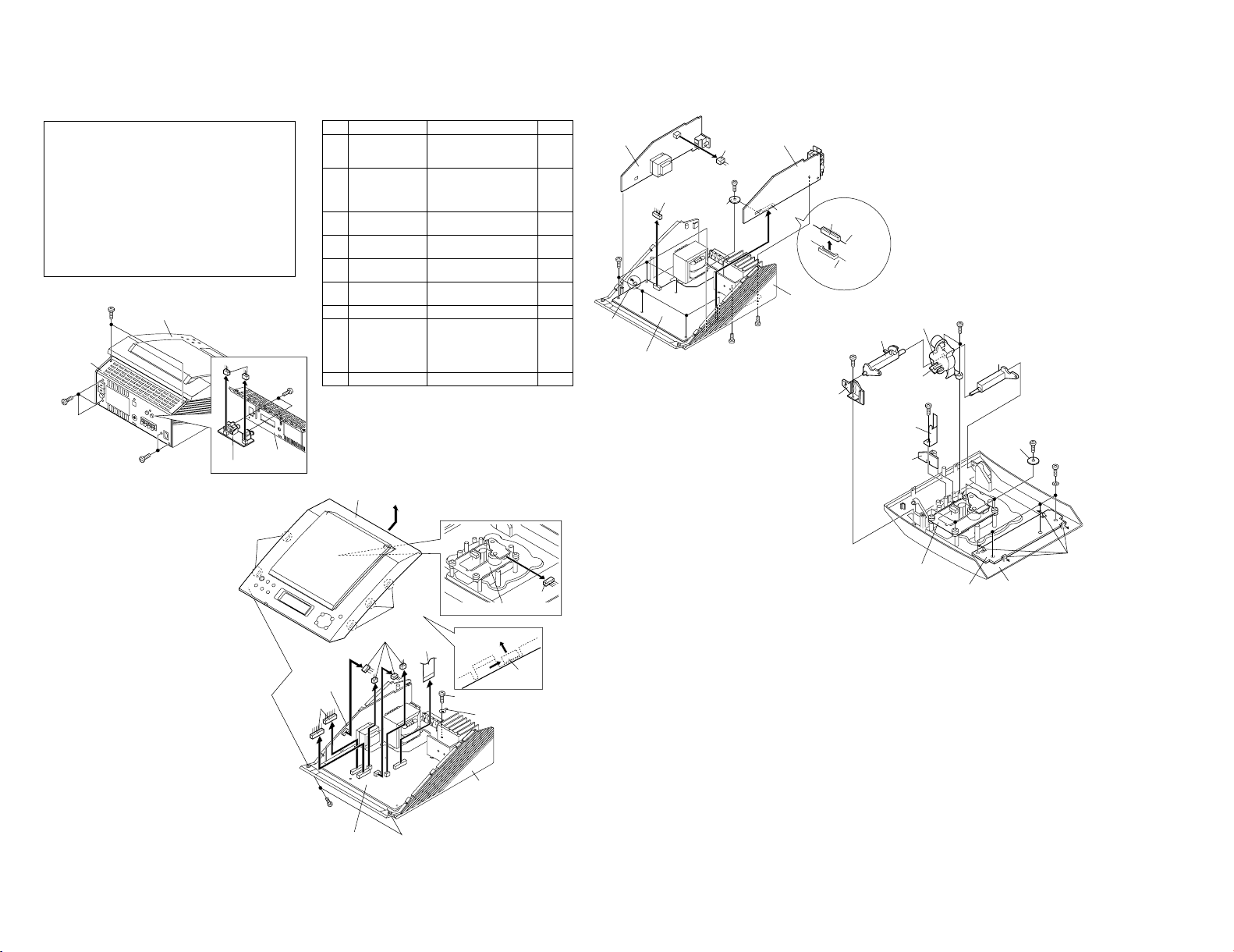
1
Rear panel/Terminal PWB
1. Screw .................. (A1) x7 8-1
2. Socket ................. (A2) x2
3. Screw .................. (A3) x3 8-1,2
2 Top cabinet 1. Screw .................. (B1) x2 8-2
2. Hook .................... (B2) x5
3. Flat Cable ............ (B3) x1
4. Socket ................. (B4) x7
3 Tuner PWB 1. Screw .................. (C1) x2 9-1
2. Socket ................. (C2) x1
4 Power PWB 1. Socket ................. (D1) x1 9-1
2. Hook .................... (D2) x1
5 Main PWB 1. Socket ................. (E1) x1 9-1
2. Screw .................. (E2) x8
6 Display PWB 1. Screw .................. (F1) x4 9-2
2. Hook .................... (F2) x4
7 CD Mechanism 1. Screw .................. (G1) x4 9-2
8 Gear Box 1. Screw .................. (H1) x1 9-2
2. Holder .................. (H2) x1
3. Lever ................... (H3) x1
4. Screw .................. (H4) x2
5. Lever ................... (H5) x1
9 LED PWB 1. Screw .................. (J1) x1 9-2
STEP REMOVAL
PROCEDURE
FIGURE
Note:
After removing the connector for the optical pickup from the
connector, wrap the conductive aluminium foil around the
front end of connector remove to protect the optical pickup
from electrostatic damage.
Caution on Disassembly
Follow the below-mentioned notes when disassembling
the unit and reassembling it, to keep it safe and ensure
excellent performance:
1. Take compact disc out of the unit.
2. Be sure to remove the power supply plug from the wall
outlet before starting to disassemble the unit.
3. Take off nylon bands or wire holders where they need to
be removed when disassembling the unit. After servicing
the unit, be sure to rearrange the leads where they were
before disassembling.
4. Take sufficient care on static electricity of integrated
circuits and other circuits when servicing.
(A1) x2
ø3 x10mm
(A1) x3
ø3 x10mm
(A1) x2
ø3 x10mm
Rear Panel
Top Cabinet
(A2) x2
(A3) x2
ø3 x10mm
Rear Panel
Terminal PWB
Figure 8-1
(B1) x2
ø2.5 x8mm
(B4) x2
(A3) x1
ø3 x8mm
Lug
(B4) x4
(B3) x1
Hook
(B2) x3
HOOK
(B2) x2
(B4) x1
CD Mechanism
Main PWB
Power PWB
Hook
Up
Slide
Bottom Cabinet
Top Cabinet
Top Cabinet
Bottom Cabinet
Figure 8-2
(C1) x1
ø3 x8mm
(E2) x7
ø3 x8mm
(E2) x1
ø3 x14mm
(D2) x1
(C1) x1
ø3 x6mm
(D1) x1
(E1) x1
Power PWB
Holder PWB
Tuner PWB
Main PWB
(C2) x1
Tuner PWB
(C2) x1
Main PWB
Hook
Bottom Cabinet
Figure 9-1
Figure 9-2
(G1) x4
ø2.5 x10mm
(H1) x1
ø3 x8mm
(H2) x1
(H5) x1
(H4) x2
ø2.5 x10mm
(J1) x1
ø2.5 x10mm
(F1) x4
ø2.5 x10mm
Hook
(F2) x4
Display PWB
LED PWB
Switch
PWB
Gear Box
CD Mechanism
Top Cabinet
Holder PWB
(H3) x1
Bracket
DISASSEMBLY FOR REPAIR
RD-M23
3
Page 4
4
How to remove the CD lid (See Fig. 10-1.)
Perform steps 1,2 and 8 of the disassembly method to remove
the gear box.(See page 8,9)
1. Remove the switch PWB.
2. Remove the screws (A1) x 4 pcs., to remove the gear box
lid.
3. Remove the gears (A2) x 1 pc. and (A3) x 1 pc.
4. Remove the screws (A4) x 2 pcs., to remove the motor.
Caution:
Be careful so that the gear is not damaged.
(The damage gear emits noise during searching.)
Figure 10-1
Figure 10-2
(A1) x1
ø2.5 x10mm
(A1) x3
ø2.5 x12mm
(A2) x1
(A3) x1
(A4) x2
ø2 x5mm
Switch PWB
CD Lid Motor
CD MECHANISM SECTION (See Fig. 10-2.)
Perform steps 1,2 and 7 of the disassembly method to remove
the CD mechanism.(See page 8,9)
1. Remove the mechanism cover, paying attention to the
pawls (A1)x 4 pcs.
2. Remove the screws (A2) x 2 pcs., to remove the shaft (A3)
x 1 pc.
3. Remove the stop washer (A4) x 1 pc., to remove the gear
(A5) x 1 pc.
4. Remove the pickup.
Note:
After removing the connector for the optical pickup from the
connector, wrap the conductive aluminium foil around the
front end of connector remove to pretect the optical pickup
from electrostatic damage.
Pickup unit
(A2) x2
ø2.6 x6mm
(A1) x4
CD Mechanism
Shaft
(A3) x1
Gear
(A5) x1
Stop Washer
(A4) x1
Mechanism Cover
RD-M23
REMOVING AND REINSTALLING THE MAIN PARTS
DISASSEMBLY FOR REPAIR
Page 5
2
1
VOLTAGE
REGULATOR
3
1
3
4
2
1
USWD_5R6V
P_CONT
D_GND
3 2 1
AC INPUT
SOCKET
AC 110/127/220/
230~240V, 50/60Hz
AC POWER SUPPLY CORD
VOLTAGE
SELECTOR
POWER
TRANSFORMER
(SUB)
FROM
DISPLAY PWB
POWER PWB-B
CNP651
SO655
SW651
IC681
KIA7805API
D688
1N4004
RLY601
CNP707
T681
D681~D684
Q683
Q681
4
3
2
1
4
3
2
1
3 5 5 7 7 9 9
1
POWER
TRANSFORMER
(MAIN)
TF
T651
T2.5A L 250V
CNP801
F651
T1.25A L 250V
F653
Q606
Q607
D651~D654
D657~D660
Q801
Q101
Q102
Q601
Q602
Q605
Q603
Q604
Q608
Q609
CD +B
CNP652
FROM
DISPLAY PWB
+B
CD_6R2V
+B2
+B3
+B4
+B6
M_12V
A_12V
POWER AMP.
IC901
LA4282
L-CH
L-CH
R-CH
R-CH
L-CH
R-CH
SPEAKER TERMINAL
+
+
SO601
HEADPHONES
1
2
3
4
5
9
10
J601
VSS
VDD
IC401
LC75342M
15
14
13 12
11
10
9
17
18
19
20
21
22
23
24
25
26
27
28
29
16
8
7
6
5
4 3 2 1
CE
DI
30
CL
LOGIC
TUN L
CD L
TUN R
R-CH OUT
L-CH OUT
A_12V
NC
FUNCTION/VOLUME
EQUALIZER
Q901 Q902
Q908 Q907
Q861
Q802
AUX R
AUX L
CD R
7654321
8
9
10
11
12 13 14 15
CNP702
CLID_SW
CLID_UP
CLID_PRO
CLID_DW
BUCK
BUS2
BUS0
BUS1
BUS3
CCE
CD_RES
PU_IN
LIGHT
CD_STB
DIMMER
SBAD
FEO
FEN
VRO
RFRP
RFIS
RFGO
RFGC
AGCI
RFO
GND
RFN
TEO
TEN
2VRO
TEB
SEL
LDO
MDI
TN1
TPI
FPI
FNI
VCC
SERVO PRE AMP.
IC801
TA2109F
SERVO/SIGNAL CONTROL
IC802
TC9462F
DOUT
TERMINAL
PWB
VSS
VSS
VSS
AVSS
XVSS
TESIOO
TESIN
TESI01
VSS
VSS
PXI
DVSL
DVSR
PDO
TMAX
VCOREV
RFI
RFCT
LPFN
LPFO
PVREV
TSIN
VREF
X801
16.93MHz
XO
XI
VDD
VDD
VDD
VDD
VDD
XVDD
AVDD
2VREF
SEL
RFGC
TEBC
FOO
TRO
TEI
TEZI
RFRP
FEI
SBAD
P2VREF
SWITCHING
MUTE
VOLTAGE
REGURATOR
VOLTAGE
REGURATOR
+B6
R-CH
L-CH
SO401
VIDEO/AUX
INPUT
CD LID
MOTOR DRIVER
1
23
5
6
7
8
9
IC805
TA7291S
11 10 9 8 7 6 5 4 3 2 1
CE
CL
DI
SD
FM ST
DO
A_12V
D_GND
TUN L
TUN R
A_GND
11
1 2 3 4 5 6
7 8 9 10
SD
STEREO
DO
CE
DI
CL
CD +B
P_MUTE
P_STB
D_GND
A_12V
+B1
+B3
+B6
+B2
+B4
CNP703
CNP307
TO
TUNER PWB
FROM
DISPLAY PWB
FROM
DISPLAY PWB
LED PWB
SWITCH PWB
CD LID
OPEN/CLOSE
SW802
CD LID
OPEN/CLOSE
MOTOR
M
M801
FOCUS/TRACKING/
SPIN/SLED DRIVER
1234
5
6
7
8
9910111213
16 17 18 19 21 22 23 24 25 26 2728
PO1-
PO1+
VO3-
VO3+
VIN3
VG3
VCC
VCC
BIAS
VG4
VIN4
VO4+
VO4-
OPO
VO2-
VO2+
VIN2
VG2
GND
GND
GND
MUTE
REG O
TRB
VG1
VIN1
VO1+
VO1-
IC804
MM1469XH
SPINDLE
MOTOR
SLED
MOTOR
PICKUP IN
SP+
SP–
SP+
SL–
PU-IN
GND
FO
TR
+
–
–
+
M
M
CD MOTOR PWB
NM802
NM801
NSW801
CD_7V
5V
+B2
+B4
+B7
+B7
+B7
A
C
B
F
E
+B7
+B7
+B7
LD
MON
FOCUS COIL
1/2V
5V
TRACKING COIL
PICKUP UNIT
23
24
22
21
20
19
18
17
16
45
40
38
34
33
32
31
30
28
50
56
57
51
52
48
49
46
47
43
42
44
15
14
13
12
11
10
9
8
7
6
5
4
3
2
1
DIGITAL
OUT
3
2
1
J801
5355
FMO
DMO
100
90
97
96
93
92
91
78
79
BUS0
BUS1
BUS2
BUS3
BUCK
/CCE
/RST
85
82
RO
LO
14
23
39
62
76
80
94
6152436 63 71 72 73 74 77 95 81 86
D_GND
A_GND D_GND
D_GND
M_GND
M_GND
M_GND
M_GND
25
MAIN PWB
AC 110/127/220/
230~240V, 50/60Hz
5 12910 11 3 7 4 2
IN2
POWER
–GND1
VCC
OUT1
FIL
OUT2
GND
NF1
110V
127V
220V
230~240V
F654
2A 250V
TF
5
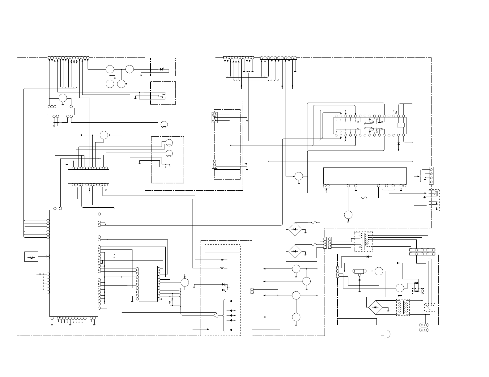
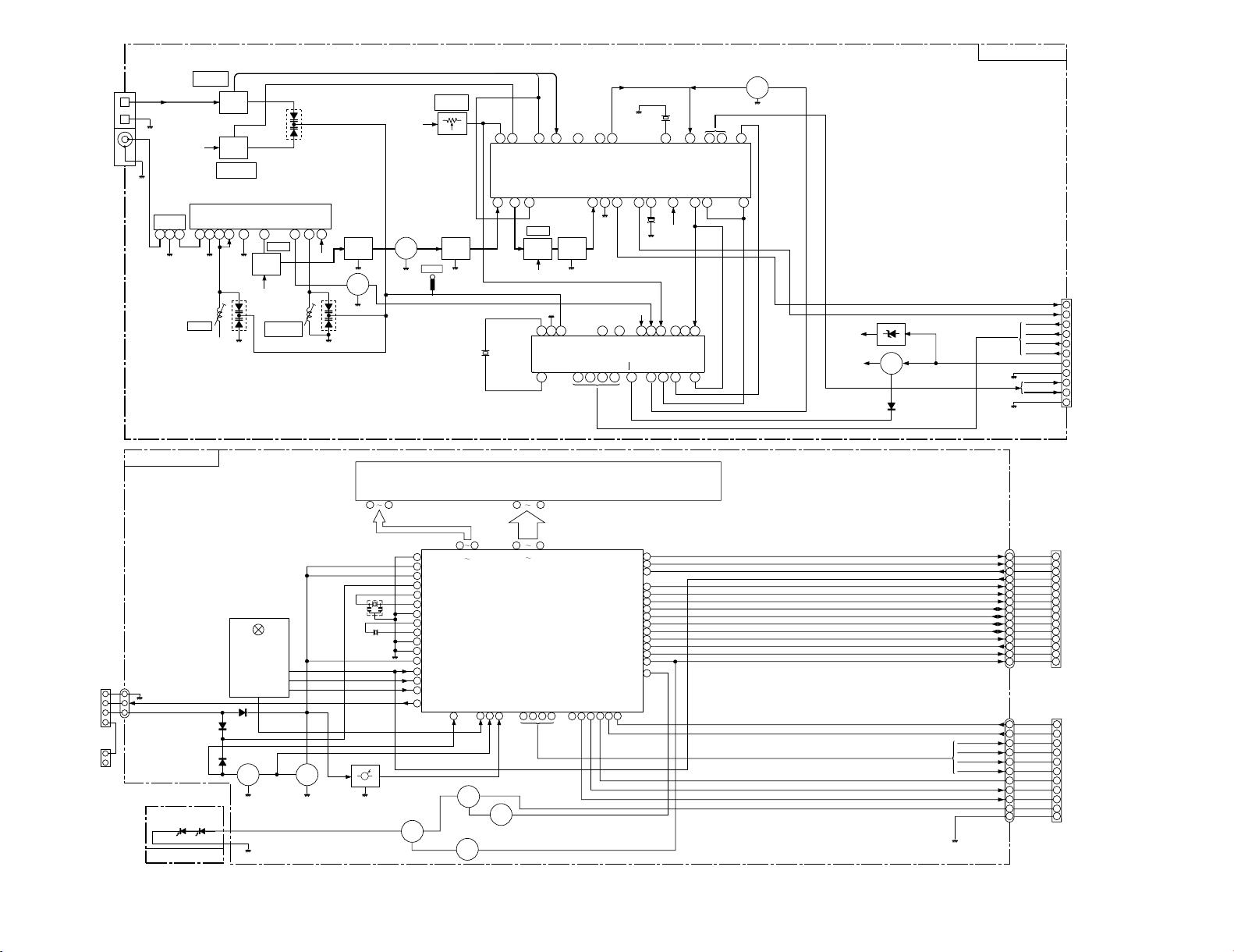
BLOCK DIAGRAM
RD-M23
Page 6
AM
GND
FM
75ohms
SO301
VSM
AM RF
OUT
OUT
OUT
OUT
IN
IN
CUT
AM LOW
FM/AM
MPX VCO
MPX IN
MO/ST
L-CH
R-CH
FM AFC
AM OSC
AM OSC
(AM/FM)
PHASE
PHASE
IF OUT
VCC
FM DET
STEREO
SD
GND
AM IF
REG
AM MIX
OUT ININ
FM IF
23 22 21 20 19 18 17 16 15 1424 13
121110987654321
PLL(TUNER)
111098765431
PD
IF IN
AM IN
FM IN
VDD
AIN
AOUT
VSS
X OUT
22 21 20 19 18 17 16 15 14 13 12
FM
FM
MUTE
CEDICL
DO
MO/ST
IF REQ
X IN
IC302
LC72131
FM FRONT END
1
2
3
4
56 7 9
8
IC301
BF301
BAND PASS
FILTER
TA7358AP
1
2
3
TP301
456kHz
X351
32.768kHz
8MHz
Q351
Q360
ZD351
10
11
1
2
3
4
5
8
9
6
7
SD
FM ST
DO
CL
CE
DI
A_12V
D_GND
TUN_L
TUN_R
A_GND
TO
MAIN PWB
CNS307
TUNER PWB
38541
1
100
67
57
56
20
59
66
65
64
63
62
61
60
58
53
54
51
39 46 49 5032
47
8
4
LCD701
LCD DISPLAY
1
2
3
4
5
6
7
8
9
10
11
12
13
14
15
LIGHT
BUS0
BUS1
BUS2
BUS3
BUCK
CCE
CD_STB
CLID_DW
CLID_UP
CLID_PRO
CLID_SW
CD_RES
PU-IN
DIMMER
LIGHT
BUS0
BUS1
BUS2
BUS3
BUCK
CCE
CD_STB
CLID_DW
CLID_UP
CLID_PRO
CD_RES
PU-IN
DIMMER
B-LIGHT
1
2
3
4
5
6
7
8
9
10
11
12
13
14
15
TO
MAIN PWB
TO
MAIN PWB
TO
POWER PWB
TO
MAIN PWB
CNS702
CNW702
REMOTE
SENSOR
RX701
3
2
1
3
4
2
1
2
1
CNW707
CNS707CNS652
RESET
VLC1
VLC2
VLC3
7
6
5
MMOD
VREF–
VREF+
VSS
15
24
14
11
SYS_STOP
POWER
3837
13
12
10
9
X701
X702
OSC1
OSC2
XO
XI
CLID_SW
SW711~713
SW721,722
SW725~727
SW709
SW718
SW710
KEY1
KEY2
18
17
16
SYSTEM MICROCOMPUTER/
FL DRIVER
IC701
IX0039SJ
D_GND
A_24V A_12V
P_STB
P_MUTE
CD+B
DI
CE
CL
DO
STEREO
SD
11
10
9
8
7
6
5
4
3
2
1
11
10
9
8
7
6
5
4
3
2
1
CNW703
CNS703
CD+B
STEREO
SD
DI
CLDOCE
28272625
SURR
P–STB
P–MUTE
454443
DISPLAY PWB
Q708
Q707
Q709
Q706
ANTENNA
TERMINAL
AM Band
Coverage fL
FM MUTE
LEVEL
AM IF
FM IF
AM
Tracking fL
FM RF
VD301
VD303
VD302
FM IF DET/
FM MPX/AM IF
IC303
LA1832S
+5V
+5V
VT
+5V
+5V
+B
FM +B
+5V
FM +B
+5V
T302
T306
T304
T351
CF303
L302
FM ANT.
FM Band
Coverage fL
FM +B
FM +B
L303
FM OSC.
CF302
FM IF
FM IF
CF352
CF351
AM IF
SWITCHING
SWITCHING
RESET
SWITCHING
Q306
Q302
Q701
Q702
Q703
VR351
X352
4.5MHz
VOLTAGE
REGURATOR
COM0
COM3
SEG0
SEG33
REMOCON
P_CONT
USWD_5R6V
D_GND
P–CONT
VDD
GND
LED701 LED702
LED PWB
6
RD-M23
BLOCK DIAGRAM
Page 7
Cleaner Liquid
Cleaning Disc
PARTS CODE: UDSKA0004AFZZ
HOW TO USE
1. Using the brush in the cleaner cap, apply 1 or 2 drops of the cleaning fluid to the brush on the CD cleaner disc which has
the mark next to it.
2. Place the CD cleaner disc onto the CD disc tray with the brush side down, then press the play button.
3. You will hear music for about 20 seconds and the CD player will automatically stop. If it continues to turn, press the stop button.
CAUTION
The CD lens cleaner should be effective for 30 - 50 operations, however if the brushes become worn out earlier then please
replace the cleaner disc.
If the CD cleaner brushes become very wet then wipe off any excess fluid with a soft cloth.
Do not drink the cleaner fluid or allow it to come in contact with the eyes. In the event of this happening then drink and / or
rinse with clean water and seek medical advice.
The CD cleaner disc must not be used on car CD player or on computer CD ROM drives.
All rights reserved. Unauthorized duplicating, broadcasting and renting product is prohibited by law.
When the CD does not function
When the CD section does not operate when the objective lens of the optical pickup is dirty, this section may not operate. Clean
the objective lens, and check the playback operation. When this section does not operate even after the above step is taken,check
the following items.
Remove the cabinet and follow the troubleshooting instructions.
"Track skipping and/or no TOC (Table Of Contents) may be caused by build up of dust other foreign matter on the laser pickup
lens. Before attempting any adjustment make certain that the lens is clean. If not, clean it as mentioned below."
Turn off the power, and wipe the lens softly using a cleaning paper moistened with commercially available cleaning solution so
as not to damage it.
Be careful not to touch the lens with bare hands.
Dust gradually accumulates on the objective lens during use, and it may degrade performance.
To avoid this problem, use a cleaning disc designed for CD optical pickup lenses.
Make sure that the disc is normal, and set the CD TEST MODE (STEP 1).
Is the measured voltage as specified in circuit diagram?
Check the main unit power supply circuit.
No
Yes
No
Is "Er-CD01" displayed"?
Yes
Move the pickup to most internal circumference side of disc.
Turn the power off and reset the CD TEST MODE (STEP 1).
Is "PU ERROR " not displayed?
Yes
Check the PWB pattern between pin 59 (CD_RES) of IC701 and
pin 100 (/RST) of IC802.
No
Is +5V applied to pin 100 (/RST) of IC802?
Yes
Is CD Lid switch SW802
ON condition ?
No
Does the CD TEST MODE advance from "STEP 2"?
Yes
Check the between pattern IC701 and SW802 If OK.
Check the main unit power supply circuit.
No
Does the laser come on in CD TEST MODE "STEP 2"?
Check the procedure in "LASER FAILURE".
Yes
Does the CD TEST MODE advance from "STEP 3" to "STEP
4"?
Check the procedure in "FOCUS FAILURE".
Yes
Yes
Does the spindle motor rotate normally when the CD TEST
MODE changes from "STEP 4" to "STEP 3"?
Yes
Is the HF output on pin 38 of IC802 in CD TEST MODE "STEP 5"?
Check the procedure "HF ERROR".
Yes
No
No
No
No
Check the pattern between pin 58 (PU_IN) of IC701 and
CNW803/CNS803.
Check the between CNW803/CNS803 and PU-IN switch.
Set ON condition the CD
Lid switch.
Check the procedure in "SPINDLE MOTOR CLV SERVO
FAILURE".
No
Does the sled motor
move ?
No
Does the sound heard when the optical pickup move to the
selected play by the FF
/REW key.
Check the procedure "NO SOUND"
No
Yes
Check the procedure in
"SLED MOTOR
OPERATING FAILURE ".
Does the LCD track number and time indicator work properly ?
Check the pattern between IC701 and LCD701.
Yes
No
Is "Er-CD01 "
displayed ?
No
Turn the power off and then back on.
Does the unit initialize properly and start playback when PLAY
key is pressed?
Check the pattern between pin 58 (PU_IN) of IC701
and CNW803/CNS803. Check the between CNW803/
CNS803 and PU-IN switch.
No
Yes
Check the procedure in
"HF ERROR".
Yes
Does the unit play in order in the FF mode?
Check the procedure in "TRACK SEARCH FAILUR".
Yes
Does playback continue for 30 seconds after the start of
playback ?
Check the procedure in "SLED SERVO FAILURE".
Yes
Normal
No
No
Yes
TROUBLE SHOOTING
RD-M23
7
Page 8
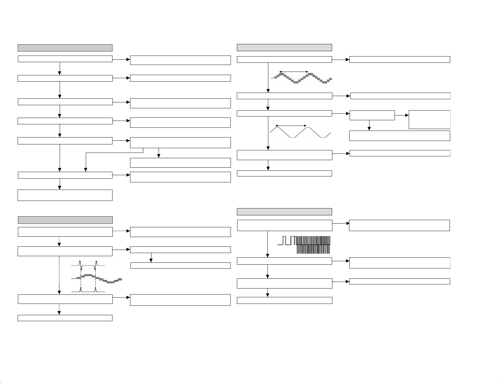
8
Check the PWB pattern between emiter of Q607 and emiter of
Q861.
• Laser failure.
Is 0V applied to the pin 57 (SEL) of IC802 ?
Yes
No
Does the laser come on when pattern cut between pin 8 (SEL) of
IC801 and pin 57 (SEL) of IC802 ?
Check the PWB pattern between IC701 and IC802 (BUCK/CCE/
BUS0~3)
Yes
Yes
No
Check the peripheral parts of IC801 and Q801. If it is normal, the
optical pickup is faulty.
No
Check CNP802/CNW3. If it is normal, the optical pickup is
faulty.
Is approx. 2V applied to the collector of Q801.
• Focus failure.
Does the optical pickup move up and down when the disc is
removed?
Is the following waveform ouput at the pin 43 (FEI) of IC802
when the disc is set?
Is the waveform shown above input at the pin 44 (SBAD) of
IC802?
Yes
Yes
No
No
The optical pickup is faulty.
Check as stated in item "FOCUS SERVO SAWTOOTH WAVE
FAILURE".
Yes
Check the periphery of IC801 and CNP802/CNW3. Is it normal?
No
Check the pattern between pin 13 of IC801 and pin 44 of IC802.
Check the periphery of IC801 and CNP802/CNW3.
IC801 is faulty.
Yes
Is +6.2V applied to the emiter of Q861 ?
Is +5V applied to the collector of Q861 ?
Yes
No
No
Check the peripheral parts of IC804 and Q861.
Is +5V applied to the pin 62 (VDD) of IC802 ?
Is +5V applied to the pin 1 (VCC) of IC801 ?
Yes
No
No
Check the PWB pattern between collector of Q861 and pin 62 of
IC802.
Check the PWB pattern between collector of Q861 and pin 1 of
IC801.
pin 43
(FEI)
pin 48
(FOO)
pin 44
(SBAD)
Yes
Yes
• Focus servo sawtooth wave failure.
Is +6.2V applied to the pins 21 and 22 (VCC) of IC804 ?
Is sawtooh wave output to the pin 48 (FOO) of IC802 ?
IC802 is faulty.
No
Yes
Yes
Is sawtooth wave obtained between pins 26 and 27 of IC804 ?
No
No
Check the PWB pattern
between pin 7 of IC804
and pin 60 (CD STB) of
IC701.
Is +5V applied to the pin 7
(MUTE) of IC804 ?
Check the PWB pattern between pin 48 (FOO) of IC802 and pins
24 and 25 of IC804. If OK. IC804 is faulty.
Check the PWB pattern between pin emiter of Q607 and IC804.
No
Is sawtooth wave obtained between pins 13 and 16 of
CNP802/CNW3 ? (as shown above)
Yes
Check the PWB pattern between CNP802/CNW3 and IC804.
No
CNP802/CNW3 connection failure or optical pickup failure.
Yes
• Spindle motor clv servo failure.
Is above wave obtained between pins 11 and 12 of IC804 ?
Is following wave output to the pin 55 (DMO) of IC802 when
the CD TEST MODE "STEP 3" is changed to " STEP 4" ?
No
Yes
Check the procedure in "HF ERROR".
If OK. IC802 is faulty.
Check the PWB pattern between pin 55 (DMO) of IC802 and pins
9 and 10 of IC804. If OK. IC804 is faulty.
No
Is above wave obtained between pins 9 and 12 of CNP802/
CNW3 ?
Yes
Check the PWB pattern between CNP802/CNW3 and IC804.
No
CNP802/CNW3 connection failure or optical pickup failure.
Yes
DMO
Yes
1.5~2.5sec
1.5~2.5sec
RD-M23
TROUBLE SHOOTING
Page 9
• HF error.
Yes
Yes
Is output (tracking error signal) obtained at the pins 46 (TEI)
and 47 (TEZI) of IC802 the CD TEST MODE "STEP 4" is
changed to "STEP 5"?
Is output (HF signal) obtained at the pin 38 (RFI) of IC802
when the CD TEST MODE "STEP 4" is changed to "STEP 5"?
Is output (HF signal) obtained at the pins 41 (RFZI) and 42
(RFRP) of IC802 when the CD TEST MODE "STEP 4" is
changed to "STEP 5"?
No
No
• No sound.
No sound from both L and R-ch?
Yes
Is +4.5V applied to pin 83 (DVDD) of IC802?
No
Check the PWB pattern between pin 49 (TRO) of IC802 and pin 19
of IC804.
Check the periphery of IC804 and CNP802/CNW3.
If OK. Optical pickup failure.
Check the periphery of IC801.
Check the PWB pattern between pin17 (RFRP) of IC801 and pins
41 (RFZI) and 42 (RFRP) of IC802.
If OK. IC801 is faulty.
No
Yes
Normal.
Check the interval between the pins 82 or 85 of IC802 and the pins
2 or 5 of IC901.
No
Check the PWB pattern between R819 and Q861.
Yes
Is signal of pins 82 and 85 of IC802 output?
No
Check the peripheral parts of IC802. If OK, IC802 is faulty.
Yes
The main PWB is faulty.
Check the periphery of IC801.
Check the PWB pattern between
pin 12 (TEO) of IC801 and pins 46
and 47 of IC802.
Is it normal ?
Is output obtained at the pins 3 and
8 of CNP802/CNW3.
Optical pickup failure.
IC801 is faulty.
Check the periphery of IC801.
Check the PWB pattern between pin 19 (RFGO) of IC801 and pins
38 (RFI) of IC802.
If OK. IC801 is faulty
Is output obtained at the pins 4 and
5,6 of CNP802/CNW3.
Optical pickup failure.
Is the following wave output to the pin 55 (DMO) of IC802
when the CD TEST MODE "STEP 4" or "STEP 5"?
Check the periphery pins 28~32 of IC802.
If OK. IC802 failure.
No
No
No
Yes
Yes
No
Yes
Yes
test mode "step 4" test mode "step 5"
TEI
TEZI
test mode "step 4" test mode "step 5"
RFI
test mode "step 4" test mode "step 5"
RFZI
RFRP
test mode "step 4" test mode "step 5"
DMO
• Sled motor operation failure.
Yes
Yes
Is following sled feed signal output the pin 53 (FMO) of IC802
when FF
/REW key is pressed after the CD TEST
MODE "STEP 1" is seted?
Is sled feed signal output the pins 1 and 2 of IC804?
Is sled feed voltage applied between both terminals of sled
motor?
No
Check the peripheral parts of IC804. If OK, IC804 is faulty.
No
C801 is faulty.
Check the CNW803/CNS803.
No
Yes
Check the CD mechanism (periphery of sled motor).
If the sled motor does not run when DC2.0V is applied to
both terminals of sled motor, the sled motor is faulty.
• Sled servo failure.
Yes
Is following sled signal output the pin 53 (FMO) of IC802
during playback?
Normal.
No
IC802 is faulty.
• Track search failure
Does the sled motor run in FF/REW state when the SERVO
TEST MODE "STEP1" is set?
Is the following wave output to the pin 49 (TRO) of IC802
during track search in normal playback?
Is the following wave output to the pins 12 (TEO) of IC801
during track search in normal playback?
Yes
Yes
No
Check as stated in item "SLED MOTOR OPERATION FAILURE".
No
IC802 failure.
No
Check the PWB pattern between pin 49 (TRO) of IC802 and pin
19 of IC804.
Check the PWB pattern between pins 17 and 18 of IC804 and
Optical pickup.
If OK. Optical pickup failure.
Yes
Is the above wave output to the pins 46 (TEI) and 47 (TEZI) of
IC802 during track serch in normal playback?
No
Check the PWB pattern between pin 12 (TEO) of IC801 and pins 46
and 47 of IC802. If OK. IC801 failure.
Normal.
Yes
Yes
Is following sled feed signal output the pins 3 and 4 of IC804
when FF
/REW key is pressed after the CD TEST
MODE "STEP 1" is seted?
Check the PWB pattern between pin 53 of IC802 and pins 3 and 4
of IC804.
No
Is the following wave output to the pin 41 (RFZI) and 42
(RFRP) of IC802 during track search in normal playback?
No
Check the PWB pattern between pin 17 (RFO) and 18 (RFIS), 19
(RFRP) of IC801 and pins 41 and 42 of IC802. If OK. IC801 failure.
Yes
TRO
TEO
TEI
TEZI
FF REW
FMO
FMO
RFZI
RFRP
FF REW
SL ±
9
TROUBLE SHOOTING
RD-M23
Page 10

10
2. CD Test Mode (TEST 1)
In the CD test mode the operation of each step is possible even if the LID-SW is off. If focus cannot be taken in step 3 or any error
is processed, it is impossible to proceed to the next step. During error processing, end the test mode by pressing the ON/STANDBY button or return to the step 1 by pressing the CD STOP button. Any other operations are inhibited.
1. Step 1 Mode
When the CD test mode is obtained, the following display lights up. Then CD initialization operation flow proceeds up to CD
STB off to wait for the following buttons to be pressed.
One second after display lights up
Press the following buttons in this state to obtain the operations specified below.
"POWER" .................Test mode and power turned off to shift to the ordinary standby mode.
"FF/FWD" .................After the pickup returns to the innermost periphery, it slides toward the outer periphery while this button
is pressed.
"REW/REV" ..............After the pickup returns to the innermost periphery, it slides toward the inner periphery while this button
is pressed. If PICKUP IN is on, input is invalid.
"PLAY" ..................... Shift to step 2
"STOP" ..................... Invalid
"FUNCTION" ............ Shift to step 5
* In case of initialization, the pickup is moved toward the inner periphery. Any buttons other than "ON/STAND-BY" button are
not accepted until the shift of pickup to the inner periphery is completed at this time. If PICKUP IN SW ON cannot be detected
within 10 seconds, the slide motor stops, and the following error display appears. Press the ON/STAND-BY button to end
the test mode, or press the CD STOP button to return to step 1. Any other operations are inhibited.
The test mode applied to this microcomputer has three modes, namely the ordinary test mode for adjustment or measurement,
the aging test mode, and the self-diagnosis test mode for self-judgment in case of final product inspection.
1. Turning on the test mode
For obtaining each test mode, press the ON/STAND-BY button, while keeping pressing the following two buttons in the ordinary
stand-by mode (power off ). In this case, the main unit buttons are valid. When turning the ON/STAND-BY on with remote control
buttons, test modes are not obtained.
[Ordinary test mode]
1. CD Test Mode (TEST 1).....................................REW/PRESET DOWN + VOLUME UP
2. Tuner Test Mode (TEST 2).................................REW/PRESET DOWN + CD PLAY
3. Electronic Volume Test Mode (TEST 3)............. REW/PRESET DOWN + FF/PRESET UP
4. Timer Test Mode (TEST 4).................................FUNCTION + VOLUME UP
5. LCD Test Mode (TEST 5)...................................FUNCTION + FF/PRESET UP
6. Electric CD Lid Aging Test Mode (TEST 8)........ FUNCTION + CD PLAY
FUNCTION + VOLUME DOWN
[Self-diagnosis Test Mode]
1. Button input diagnosis test mode (TEST6).…....
Processes are different depending on destinations at initial settings.
The time display always indicates "0:00".
Press the following buttons in this state to obtain the operations specified below.
"POWER" ................ Test mode and power turned off to shift to the ordinary standby mode.
"FF/FWD" ................ The pickup slides toward the outer periphery while this button is pressed.
"REW/REV" .............The pickup slides toward the inner periphery while this button is pressed. If PICKUP IN is on, input is
invalid.
"PLAY" ..................... Shift to step 5
"STOP" .................... Return to step 1
"FUNCTION" ........... Shift to step 5
*If the focus is not received, the process returns to step 1.
4. Step 4 Mode
The CLV servo ON command (8600) is transmitted to wait for the following buttons to be pressed. (The disc is rotated for CLV
lock.)
Press the following buttons in this state to obtain the operations specified below.
"POWER" ................ Test mode and power turned off to shift to the ordinary standby mode.
"FF/FWD" ................ The pickup slides toward the outer periphery while this button is pressed.
"REW/REV" .............The pickup slides toward the inner periphery while this button is pressed. If PICKUP IN is on, input is
invalid.
"PLAY" ..................... If focus has been taken, shift to step 4 is executed. If not, acceptance is inhibited.
"STOP" .................... Return to step 1
"FUNCTION" ........... Shift to step 5
*If the focus is not received after it has been taken, the process returns to step 1.
3. Step 3 Mode
While the laser keeps lighting, CD initialization operation flow proceeds up to 'CLV servo ON' to wait for the following buttons
to be pressed.(Focus servo turned on for focus search)
The focus search is repeated to take focus.
Press the following buttons in this state to obtain the operations specified below.
"POWER" ................ Test mode and power turned off to shift to the ordinary standby mode.
"FF/FWD" ................ The pickup slides toward the outer periphery while this button is pressed.
"REW/REV" .............The pickup slides toward the inner periphery while this button is pressed. If PICKUP IN is on, input is
invalid.
"PLAY" ..................... Shift to step 3
"STOP" .................... Return to step 1
"FUNCTION" ........... Shift to step 5
2. Step 2 Mode
Press the "CD PLAY" button in this mode to transmit the laser lighting command LDON (8400) and turn on the laser. Any other
operations are not performed in this case.
RD-M23
TEST MODE
Page 11

Press the following buttons in this state to obtain the operations specified below.
"POWER" .................Test mode and power turned off to shift to the ordinary standby mode.
"FF/FWD" .................The pickup slides toward the outer periphery while this button is pressed.
"REW/REV"..............The pickup slides toward the inner periphery while this button is pressed. If PICKUP IN is on, input is
invalid.
"PLAY" ..................... Invalid
"STOP" ..................... Return to step 1
"FUNCTION" ........... Shift to step 6
"MEMORY" .............. Shift to step 7
*If the is not received, the process returns to step 1.
Other cautions
• TOC IL is not available for this test mode.
5. Step 5 Mode
When the CD initialization operation flow is completed, the mute is turned off, and playback is started. Even if playback
reaches the outermost periphery of disc, the operation does not stop. The LCD display indicates the playback passage time
as in case of ordinary CD playback.
Press the following buttons in this state to obtain the operations specified below.
"POWER" .................Test mode and power turned off to shift to the ordinary standby mode.
"FF/FWD" .................The pickup slides toward the outer periphery while this button is pressed.
"REW/REV"..............The pickup slides toward the inner periphery while this button is pressed. If PICKUP IN is on, input is
invalid.
"PLAY" ..................... Invalid
"STOP" ..................... Return to step 1
"FUNCTION" ........... Shift to step 5
"MEMORY" .............. Shift to step 7
Press FF/PRESET UP or REW/PRESET DOWN button to slide the pickup. The number of errors accumulated up to that time
is cleared and addition is restarted after shift.
*If the focus is not received, the process returns to step 1.
6. Step 6 Mode
Press the FUNCTION button during step 5 operation to set EC/FC bit to "H" by PROSET command (9188 transmission) and
to monitor BUS2 (QDRE) during idle mode. The number of errors for 1 frame (1 sub-code block in IC data) is read by read
command SRC6 during "H". The number of errors accumulated in 750 frames for 10 seconds is displayed on LCD. During
the display, music signal is played back.
Press the following buttons in this state to obtain the operations specified below.
"POWER" .................Test mode and power turned off to shift to the ordinary standby mode.
"FF/FWD" .................The pickup slides toward the outer periphery while this button is pressed.
"REW/REV" ..............The pickup slides toward the inner periphery while this button is pressed. If PICKUP IN is on, input is
invalid.
"PLAY" ..................... Invalid
"STOP" ..................... Return to step 1
"FUNCTION" ........... Shift to step 6
"MEMORY" .............. Shift to step 5
*If the focus is not received, the process returns to step 1.
7. Step 7 Mode
Press "MEMORY" key during step 6 operation to display automatically adjusted values on LCD in the order as below. Item
names are displayed by left alignment, and adjusted values by right alignment in hexadecimal numbers. Operations other
than display are as same as those for step 5.
a) "Fb" is displayed on the left of LCD. FTBAST command (D480) is transmitted to designate focus balance adjusting
register. Then data read by read command SRC2 (2) are displayed in hexadecimal numbers. After waiting 2 seconds,
operation is shifted to (b).
b) "FG" is displayed on the left of LCD. FTBAST command (D481) is transmitted to designate focus gain adjusting register.
Then data read by read command SRC2 (2) are displayed in hexadecimal numbers. The upper two bits, which are invalid,
are displayed as "00". After waiting two seconds, operation is shifted to (c).
c) "Tb" is displayed on the left of LCD. FTBAST command (D482) is transmitted to designate tracking balance adjusting
register. Then data read by read command SRC2 (2) are displayed in hexadecimal numbers. After waiting 2 seconds,
operation is shifted to (d).
d) "TG" is displayed on the left of LCD. FTBAST command (D483) is transmitted to designate tracking gain adjusting register.
Then data read by read command SRC2 (2) are displayed in hexadecimal numbers. The upper two bits, which are invalid,
are displayed as "00". After waiting 2 seconds, operation is shifted to (e).
e) "FO" is displayed on the left of LCD. FTBAST command (D484) is transmitted to designate focus offset adjusting register.
Then data read by read command SRC2 (2) are displayed in hexadecimal numbers. After waiting 2 seconds, operation
is shifted to (f).
f) "TO" is displayed on the left of LCD. FTBAST command (D485) is transmitted to designate tracking offset adjusting
register. Then data read by read command SRC2 (2) are displayed in hexadecimal numbers. After waiting 2 seconds,
operation is shifted to (g).
g) "FF" is displayed on the left of LCD. FTBAST command (D486) is transmitted to designate RF amplitude adjusting register.
Then data read by read command SRC2 (2) are displayed in hexadecimal numbers. After waiting 2 seconds, operation
is shifted to (a).
TEST MODE
RD-M23
11
Page 12

12
3. Tuner Test Mode (TEST 2)
1. Outline of tuner (radio) test mode
The tuner test mode is intended to store the adjustment and measurement frequencies in the preset memory CH. When
adjusting the tuner section in the production line, adjusting personnel are not required to set frequency.
2. Details of tuner test mode
Press the "REW/PRESET DOWN" and "CD PLAY" buttons in POWER OFF state and turn on the power by the use of "ON/
STAND-BY" button to preset and store frequency for adjustment and measurement of destination specified by the AREA
terminal in the preset memory CH. However, Ordinary 1 and Ordinary 2 are stored in the destinations (selected by SPAN
switching operation) when the test mode is obtained.
("FF
" + "MEMORY/SET" KEY SPAN CHANGE)
(As for frequencies to be preset and stored for each destination, refer to item 3.)
The tuner test mode is started from preset No.1.
The operations of test mode are identical with the ordinary operations of TUNER function. FUNCTION switching is invalid.
It is necessary to discard the content of preset memory when the tuner test mode is ended; be sure to write "0000" or "1111"
bits in the memory to be checked for judging memory error at initial setting and to initialize memory.
When the tuner test mode is obtained, the following display lights for one second.
• The TUNER TEST2 mode is obtained with >> + MEMORY + ON/STAND-BY. ->Turn off AC in the TEST2 mode to restore
the initial state.
Turn off POWER to protect the memory of TEST2 mode.
Turn off POWER again to obtain the ordinary operation while the data is stored in the memory (besides
TUNER).
If AC OFF state is maintained in this state for about 1/2 day, start is executed in the initial state.
• To clear the whole memory, insert the AC cord, pressing MEMORY + CD PLAY.
3. Preset frequencies for various destinations (random preset memory)
• The slant line sections of the table store no memory.
BAND
16-25
26 FM106.00 MHz
27 FM 90.00 MHz
28 FM FM 98.00 MHz
29 MONO FM108.00 MHz
30 FM 87.50 MHz
FM
CH
BAND
1 FM 87.50 MHz
2 FM108.00 MHz
3 FM FM 98.00 MHz
4 STEREO FM 90.00 MHz
5 FM106.00 MHz
FM
CH
BAND
6 AM 522 kHz
7 AM1620 kHz
8 AM AM 990 kHz
9 AM 603 kHz
10 AM1404 kHz
AMCH
4. Electronic volume Test Mode (TEST 3)
When this test mode is obtained, the following display lights for one second.
In this mode, volume is -14 dB (STEP28), BASS/TREBLE is set to 0 (0 dB) and SURROUND mode to OFF, and start-up function
to CD, respectively. The button operations in the test mode are the same as those of ordinary operation except volume UP/
DOWN.
(1) The display is the same as that of ordinary operation except test mode setting.
(2) Unlike the ordinary state, the volume is controlled with the volume UP/DOWN button in accordance with the following three
steps.
Volume-
∞
(STEP 0) <-> Volume-14 dB (STEP 23) <-> Volume-0 (STEP 30)
(3) BASS/TREBLE and SURROUND are switched when button is pressed..
Set the current time and timer time according to the following procedure to reproduce the timer.
1.Set the current time to 1:00, the timer to ON time 1:05, the function to CD, and volume to STEP 12, respectively. One minute
is counted as one second, and the timer is reproduced. The fade-in (when playback is started) is executed at a rate of one step
for 1 sec. After completion of fade-in, the fade-out is executed at a rate of one step for 1 sec (WAIT 1 sec inserted).
After completion of fade-out, the power is turned off (after WAIT 1 sec), and the mode is shifted to the standby.
The display during operation is the same as that of ordinary timer operation.
5. Timer test Mode (TEST 4)
When this test mode is obtained, the following display lights for one second.
6. LCD Test Mode (TEST 5)
When the LCD test mode is obtained, all the LCD segments are lighted. Then pressing the "PLAY" button switches display as
below.
Lighting of all segments Lighting of odd segments Lighting of even segments
RD-M23
TEST MODE
Page 13

This test mode is intended to check whether all the main unit buttons can be detected. Accordingly, in this test mode, it is checked
whether the "ON/STAND-BY" button was pressed after all the buttons shown below were pressed. If the result is OK, OK is
displayed. If any one of keys was not pressed, an error is displayed. In both cases of OK termination or error termination, the
mode is shifted to the standby mode if the "ON/STAND-BY" button is pressed subsequently.
All models using this type of microcomputer are not always provided with the same buttons. Since the buttons used are different
depending on models, types of buttons to be used are determined by whether RDS, SURROUND, and an electric lid are
available at the initial setting by MODEL port.
The order of buttons to be pressed is not determined. Accordingly, it is checked whether all buttons have been pressed.
1. PU-IN buttons: REW/PRESET DOWN + CD STOP
Since this model is provided with SURROUND (HAVE OR NOT), RDS (HAVE OR NOT), and electric CD lid, the following
10 buttons are detected as all buttons.
PLAY, BASS/TREBLE, FUNCTION, VOLUME UP/DOWN, MEMORY/SET, REW, FF, STOP, CD-OPEN/CLOSE
The OK/NG display of test result is as follows.
7. Button input diagnosis Test Mode (TEST 6)
When the test mode is obtained, the following is displayed.
a. POWER ON for function AUX
CD lid position is checked.
CLOSE position: Operation proceeds to the next process.
Position other than CLOSE: After the lid moves to CLOSE, operation proceeds to the next process.
b. CD lid operation started
OPEN operation
WAIT 1 second
CLOSE operation
WAIT 1 second
c. Operations above are repeated.
Specified monitoring time
OPEN operation: 5 seconds
CLOSE operation: 5 seconds
8. Electric CD lid Aging Test Mode (TEST 8) (Only for model with electric CD lid)
Outline
OPEN/CLOSE operations of electric CD lid are repeated. The number of repeated times and time period are monitored. If the
lid does not move to the regular position after the specified time, operation is stopped. When an error is detected by [CLID_PRO]
during CLOSE, operation is also stopped.
d. Display
OPEN>CLOSE is counted as 1. I to 59999 are counted; if the count is over
59999, display is returned to 0 to repeat counting.
Display when the lid does not move to the regular position after the specified
time
(Ex: Defective operation occurring in the middle of 1538.)
Highlight display of stop when an error is detected by [CLID-PRO]
(Ex: Defective operation occurring in the middle of 1538.)
TUNER SECTION
Adjusting
Parts
Display
Frequency
• Setting the Test Mode
Keeping the REW/PRESET DOWN button and CD PLAY
button pressed, turn on ON/STAND-BY. Then, the frequency is initially set in the memory as shown in Table. Call it
with the REW or FF button to use it for adjustment and check
of tuner circuit.
Preset No.
FM
Preset No.
AM
1 87.50 MHz 6 522 kHz
2 108.00 MHz 7 1,620 kHz
3 98.00 MHz 8 990 kHz
4 90.00 MHz 9 603 kHz
5 106.00 MHz 10 1,404 kHz
• FM Mute Level
Signal generator: 1 kHz, 40 kHz dev., FM modulated
*1. Adjust so that an output signal appears.
Check Point Instrument
Connection
Display
Frequency
87.5 MHz 87.5 MHz 2.2 V ± 0.7 V TP301
108 MHz 108 MHz 7.3 V ± 1.0 V TP301
• Check FM VT
Signal generator: 1 kHz, 40 kHz dev., FM modulated
98.00 MHz 98.00 MHz VR351*1 Input: SO301
(30 dBµV) Output: Speaker
Terminal
Instrument
Connection
*1. Input: Antenna, Output: Speaker Terminal
*2. Input: Input is not connected, Output: TP301
Frequency
Frequency Display
Setting/
Adjusting
Parts
Instrument
Connection
AM IF 450 kHz 1,620 kHz T351 *1
AM Band — 522 kHz (fL): T306 *2
Coverage 1.1 ± 0.1 V
AM 990 kHz 990 kHz (fL): T302 *1
Tracking
fL: Low-range frequency
fH: High-range frequency
Signal generator: 400 Hz, 30%, AM modulated
• AM IF/RF
ADJUSTMENT
TEST MODE
TEST MODE / ADJUSTMENT
RD-M23
13
Page 14

RD-M23
NSW801 PICKUP IN ON—OFF
SW709 ON/STAND-BY ON—OFF
SW710 CD LID OPEN/CLOSE ON—OFF
SW711 FF/PRESET UP ON—OFF
SW712 CD PLAY/PAUSE/TUNING UP ON—OFF
SW713 VOLUME UP ON—OFF
SW718 VOLUME DOWN ON—OFF
• The indicated voltage in each section is the one measured
by Digital Multimeter between such a section and the chassis with no signal given.
1. In the tuner section,
( ) : AM mode
: FM stereo mode
2. In the CD section, the CD is stopped.
• Parts marked with “ ” ( ) are important for
maintaining the safety of the set. Be sure to replace these
parts with specified ones for maintaining the safety and
performance of the set.
• Resistor:
To differentiate the units of resistors, such symbol as K and
M are used: the symbol K means 1000 ohm and the symbol
M means 1000 kohm and the resistor without any symbol is
ohm-type resistor. Besides, the one with “Fusible” is a fuse
type.
• Capacitor:
To indicate the unit of capacitor, a symbol P is used: this
symbol P means micro-micro-farad and the unit of the
capacitor without such a symbol is microfarad. As to
electrolytic capacitor, the expression “capacitance/withstand
voltage” is used.
(CH), (TH), (RH), (UJ): Temperature compensation
(ML): Mylar type
(P.P.): Polypropylene type
• Schematic diagram and Wiring Side of P.W.Board for this
model are subject to change for improvement without prior
notice.
REF. NO DESCRIPTION POSITION POSITIONREF. NO DESCRIPTION
SW721 BASS/TREBLE ON—OFF
SW722 MEMORY SET ON—OFF
SW725 CD STOP/TUNING DOWN ON—OFF
SW726 REW/PRESET DOWN ON—OFF
SW727 FUNCTION ON—OFF
SW802 CD LID ON—OFF
ECB
(S)(G) (D)
FRONT
VIEW
FRONT
VIEW
BCE
FRONT
VIEW
2SB562 C
2SC380 O
KRA102 M
KRC102 M
KRC104 M
KRC107 M
KTA1266 GR
KTC3199 GR
KTC3200 GR
2SD2012 Y
DB5306X
SLI343YC
AUY3333
SVC348S
1 2 3
(1) (2) (3)
Figure 19 TYPES OF TRANSISTOR AND LED
NOTES ON SCHEMATIC DIAGRAM
14
Page 15

NO DISC FOCUS SEARCH STOP PLAY
FOO
1 TMAX 1
IC802 48pin
FO+ 2
SBOK
2
IC804 26pin
IC802 12pin
FO- 3 DMO 3
IC804 25pin
IC802 55pin
FOCUS SEARCH TOC IL STOP PLAY
SEL 1 TEI 1
IC802 57pin
FEI 2 TRO 2
IC802 43pin
IC802 49pin
TEI 3 FMO 3
IC802 46pin IC802 53pin
STOP PLAY CUE
FEI
1 TEI 1
IC802 43pin
SBAD 2 TRO 2
IC802 44pin
IC802 49pin
RFO 3 FMO 3
IC801 22pin
IC802 53pin
STOP PLAY REVIEW
FEI
1 TEI 1
IC802 43pin
RFGO 2 TRO 2
IC801 19pin IC802 49pin
RFRP 3
FMO
3
IC801 17pin
IC802 53pin
STOP PLAY TCD-782 TNO-02 PLAYBACK
TEI 1LO 1
IC802 46pin
TRO 2
IC802 49pin
RO 2
SBAD 3
IC802 44pin
1
2
3
4
6
7
11
15
16
17
IC802 85pin
IC802 46pin
IC802 46pin
IC802 46pin
IC802 30pin
5
6
5
7
8
5
9
10
6
11
12
13
14
6
11
15
6
11
15
IC802 82pin
WAVE FORM
RD-M23
See schematic diagram on address W to X.
15
Page 16

RD-M23
CAPACITORS CC 45 TH 1H 220 J
123 4 5 6
1 = Type ... ceramic, electrolytic, etc. 4 = Voltage rating
2 = Shape ... round, square, ect. 5 = Value
3 = Temp. coefficient 6 = Tolerance
• Temperature coefficient
1st Word C L P R S T U
Color* Black Red Orange Yellow Green Blue Violet
ppm/°C 0 -80 -150 -220 -330 -470 -750
2nd Word G H J K L
ppm/°C ±30 ±60 ±120 ±250 ±500
Example : CC45TH = -470 ± 60ppm/°C
• Tolerance (More than 10pF)
Code C D G J K M X Z P No code
(%) ±0.25 ±0.5 ±2 ±5 ±10 ±20 +40 +80 +100 More than 10µF - 10 ~ +50
-20 -20 -0 Less than 4.7µF -10 ~ +75
(Less than 10pF)
Code B C D F G
(pF) ±0.1 ±0.25 ±0.5 ±1 ±2
2nd word
ABCDEFGHJKV
1st word
0 1.0 1.25 1.6 2.0 2.5 3.15 4.0 5.0 6.3 8.0 1 10 12.5 16 20 25 31.5 40 50 63 80 35
2 100 125 160 200 250 315 400 500 630 800 3 1000 1250 1600 2000 2500 3150 4000 5000 6300 8000 -
• Voltage rating
• Chip capacitors
Refer to the table above.
1 = Type
2 = Shape
3 = Dimension
4 = Temp. coefficient
5 = Voltage rating
6 = Value
7 = Tolerance
Dimension (Chip capacitors)
Dimension code L W T
Empty 5.6 ± 0.5 5.0 ± 0.5 Less than 2.0
A 4.5 ± 0.5 3.2 ± 0.4 Less than 2.0
B 4.5 ± 0.5 2.0 ± 0.3 Less than 2.0
C 4.5 ± 0.5 1.25 ± 0.2 Less than 1.25
D 3.2 ± 0.4 2.5 ± 0.3 Less than 1.5
E 3.2 ± 0.2 1.6 ± 0.2 Less than 1.25
F 2.0 ± 0.3 1.25 ± 0.2 Less than 1.25
G 1.6 ± 0.2 0.8 ± 0.2 Less than 1.0
RESISTORS
• Chip resistor (Carbon)
Dimension
• Carbon resistor (Normal type)
1 = Type 5 = Rating wattage
2 = Shape 6 = Value
3 = Dimension 7 = Tolerance
4 = Temp. coefficient
Dimension (Chip resistor)
Dimension code L W T
E 3.2 ± 0.2 1.6 ± 0.2 1.0
F 2.0 ± 0.3 1.25 ± 0.2 1.0
G 1.6±0.2 0.8±0.2 0.5±0.1
Rating wattage
Code Wattage Code Wattage Code Wattage
1J 1/16W 2C 1/6W 3A 1W
2A 1/10W 2E 1/4W 3D 2W
2B 1/8W 2H 1/2W
• Capacitor value
010 = 1pF
100 = 10pF
101 = 100pF
102 = 1000pF = 0.001µF
103 = 0.01µF
PARTS DESCRIPTIONS
CC45
Color*
2 2 0 = 22pF
Multiplier
2nd number
1st number
(EX)
(EX)
(EX)
(EX)
C C 7 3 0 0 01 HS LFJ
1
234 5 6 7
(Chip)
(CH, RH, UJ, SL)
C K 7 3 0 0 01 HFFZ
1234 5 6 7
(Chip)
(B, F)
R K 7 3 0 0 02 BBEJ
1
234 5 6 7
(Chip)
(B,F)
R D 1 4 0 0 02 CBBJ
1234 5 6 7
16
L
W
T
Page 17

ACEG IBDFHJ
R609
R604
R607
R603
R613
R623
R621
R80F
R80C
R80E
R80A
C843
C849
R80B
R824
C860
R862
IC804
C858
R863
R861
C830
C825
C887
R820
C826
C827
C823
C824
C819
R814
C821
R812
C818
R811
R810
C817
IC802
C810
R809
R851
C809
R808
R807
R804
C844
C804
C820
C807
R825
R806
C812
C848
C802
C805
C801
R802
C846
R828
C863
C806
IC801
C847
R826
R874
R879
C839
R827
R905
R904
R901
R902
R624
R104
R608
R439
C872
R877
C837
R876
R831
R830
C835
C866
R855
R832
R854
R833
R834
R853
R835
R836
R852
R837
C869
C867
C868
R817
C833
C834
R818
C419
C420
C432
C431
C433
IC401
R416
R418
R422
R421
R415
R438
R417
R440
R436
R402
R401
R435
R437
C864
C865
F3895AF
165432
PICKUP IN
SPINDLE
MOTOR
SLED
MOTOR
Q607
Q602
Q601
Q101
Q102
C603
Q605
R614
C626
C624
D604
R612
Q606
C625
R611
ZD602
Q608
C629
C627
Q609
C628
R634
CNP307
R80G
L801
C841
Q801
R822
C859
C857
L806
C861
R843
R819
C840
L803
C832
R813
X801
C828
C822
Q861
C811
C842
R823
C845
C813
C829
R801
C803
C838
C871
Q907
Q802
CNP701
R829
C850
Q902
C855
Q908
Q901
R873
R821
CNP802
C620
R628
R629
D602
D603
C621
D654
R617
D651
ZD601
R109
Q603
C622
R620
R101
R619
D652
Q604
C113
C117
C104
C103
C102
C114
C112
C108
R105
R106
R102
C109
C110
C111
C101
C107
C115
C116
C118
R110
R108
R107
C119
C120
R661
R662
SO601
J601
R638
R637
L602
C616
C640
L603
C615
C614
C639
C613
SO401
J801
C852
C411
C412
D653
L802
C125
C658
D658
D657
F653
F651
C657
C651
C654
D401
CNP804
C421
C430
CNP806
C423
C429
C417
C837A
C836
CNP702
D402
D403
CNP703
C831
C862
R815
R816
R423
R425
R424
C418
C424
C402
C401
C426
C422
C407
C404
C403
C416
C408
C415
C425
CNW607
CNP801
C660
D660
D659
C659
C630
C853
CNP805
C851
CNP607
R405
R407
R406
R408
L601
SW802
CNW806
R914
LEDD801
CNW701
IC805
IC901
CNW805
CNW803
CNS805
CNS803
CNW3
CNS607
CNS804
CNW804
M801
CNS701
CNS806
NSW801
NM801
NM802
CNP803
CFW852
CNP652
F654
C121
C413
L401
CFW451
1
1
510
15
16
20 25
30
324567891011
15131314121110987654321
1
123
1
1
123
123
123456789
10 11
510
1520
24
12
1
1
1
13579
111315
2468
10121416
2
3
1
2
3
5
10
15
20
25
E
ECB
ECB
B
C
E
C
B
BCE
123
B
2A 250V
TF
C
E
B
BCE
C
E
B
C
E
1
2
3
1
2
3
30
31
35
40
45
50
51
55
60
65
70
75
1
6
90
85
95
81
80
100
5
20 25
28
14
B
BCE
C
E
15
10
13
223456789
1
2
3
4
5
6
7
8
9
10
12
11
CHASSIS
GND
LUG
(205)
CHASSIS
GND
CHASSIS
GND
6
5
4
3
2
1
WH
GY
GY
GY
GY
GY
1
2
3
1
2
3
3
2
1
1
RD
WH
3
4
3
2
1
RD
1
3
WH
1
2
3
RD
RD
WH
TO CHASSIS GND
LUG(205)
WH
1
2
3
1
2
RED
RD
BK
1
1
1
2
2
2
1
2
WH
BK
CD LID
OPEN/CLOSE
MOTOR
CD LID
OPEN/CLOSE
SPEAKER
TERMINAL
LEFT
RIGHT
HEAD
PHONES
DIGTAL
OUT
VIDEO/
AUX IN
LEFT
RIGHT
MAIN PWB-A1
TERMINAL PWB-A4
SWITCH PWB-A5
LED PWB-A6
CNS703
FROM DISPLAY
PWB-A3
P20 3-R
CNS702
FROM DISPLAY
PWB-A3
P20 5-R
CNS307
CNS652
TO TUNER
PWB-A2
FROM DISPLAY
PWB-A3
P19 1-O
P20 2-R
FROM
POWER
TRANSFORMER
P19 3-N
1
BK
GY
GY
2
3
CD MOTOR PWB-C
PICKUP UNIT(308)
16
16
16
1
1
1
T2.5A L 250V
T1.25A L 250V
BR
COLOR TABLE
RD(R)
OR
YL
GR
BL
VL
GY
WH(W)
BK
PK
BROWN
RED
ORANGE
YELLOW
GREEN
BLUE
VIOLET
GRAY
WHITE
BLACK
PINK
17
4
14
151110
12
16
13
875 9 6
1
3
2
PC BOARD (Component side view)
1
2
3
4
5
6
7
Refer to the schematic diagram for the value of resistors and capacitors.
17
18
Page 18

K LNPRTMOQS
R708
R706
R710
R711
R720B
R749
R721
R702
C703
R722
R728
C701
R723
C702
R727
R732
R729
R707
R720A
R7A6
R7A2
R7A7
C712
R7A8
C704
R7A5
R7A0
R7B0
R7A4
R7A1
R795
R783
R731
R735
R761
R774
R762
R763
R764
R765
R766
R767
R768
R769
R770
R773
R772
R750
C710
IC701
R785
R752
R789
R760
R733
R734
R738
R724
R725
R776
R777
R741
R740
C714
R739
R719
R758
R757
R718
R742
R780
R779
R781
R778
R792
R798
R793
R797
C397
R379
R381
C302
C349
C329
C331
R323
C335
C319
C305
C313
C314
C303
C308
C309
C304
C317
C310
R358
C343
R314
R302
R313
C350
R312
R316
R310
C318
C311
C312
C307
C306
R352
R308
R315
R305
R306
R304
C383
C387
R359
R365
R360
R371
C392
R372
R373
C384
C315
R374
C381
C382
R383
C395
R366
R355
C355
C351
C356
R353
R393
C354
C353
R351
C361
C360
C363
R361
C366
C369
C365
R357
R350
R356
R362
R364
D682
D684
D686
D681
C661
C688
C665
ZD684
D688
C689
R688
R689
ZD683
D689
RLY601
T681
T651
D685
R685
Q683
Q681
R686
R687
C683
D683
SW727
SW722
SW721
R7A3
X701
L702
SW726
SW711
SW710
D723
D722
R7A9
D720
SW712
D721
Q701
C715
Q702
SW725
Q703
C711
ZD701
R784
R759
R744
R786
X702
RX701
C713
R751
SW713
SW718
Q708
CNW707
R796
Q707
SW709
Q709
Q706
CFW701A
CNW703
CNW702
CNP651
SW651
IC681
CNP707
SO655
CNS707
CNS652
CNS703
CNS702
LCD701
C380
R380
C394
C301
C393
C316
D306
BF301
T302
D302
C330
C337
C362
C334
T306
D301
D305
VD301
VD303
VD302
C332
Q306
R336
CF303
CF302
VR351
T351
CF352
L353
C385
C386
L351
R387
R382
R386
D308
X352
R391
C391
Q360
R392
R385
C396
R384
R377
ZD351
R395
L352
C370
C357
C398
C352
C358
R376
Q351
CF351
C399
R363
IC303
X351
C371
C372
C364
C368
C374
C367
C373
IC302
SO301
CNS307
Q302
L302
R307
T304
R303
R309
L303
R301
IC301
R701
LED701
LED702
CFW701B
C705
AC POWER
INPUT SOCKET
POWER TRANSFORMER
(SUB)
POWER TRANSFORMER
(MAIN)
1
15
15
14
13
12
11
10
9
8
7
6
5
4
3
2
1
1
2
3
4
11
11
3
WH
BK
BK
BK
GY
GY
BK
GY
GY
GY
GY
GY
GY
GY
GY
GY
GY
GY
GY
GY
GY
GY
GY
GY
GY
GY
GY
GY
GY
BK
21
1
2
3
B
C
E
ECB
10
9
8
7
9
5
4
3
2
1
YL
BR
RD
RD
BL
WH
YL
BR
BR
VOLTAGE SELECTOR
110V
127V
220V230~240V
CNP801
TO MAIN
PWB-A1
P17 2-E
CNP703
TO MAIN
PWB-A1
P18 3-G
CNP703
TO MAIN
PWB-A1
P17 6-E
CNP702
TO MAIN
PWB-A1
P18 4-G
1
1
2
3
1
1
12
2
3
4
3
1
2
DISPLAY PWB-A3
LED PWB-A7
POWER PWB-B
ON/STAND-BY
FUNCTION
MEMORY/
SET
BASS/
TREBLE
5
10
15
20
30
35
40
45
50
55
60
65
70
80
85
90
95
100
75
76
51
25
26
1
1
2
3
4
5
6
7
8
9
10
11
12
13
14
15
16
17
18
19
20
21
22
23
24
25
26
27
28
29
30
31
32
33
34
35
36
37
38
PRESET
DOWN
FF
REW
TUNING
DOWN
CD STOP
PRESET
UP
TUNING
UP
CD PLAY/PAUSE
CD LID
OPEN/CLOSE
VOLUME
DOWN
VOLUME
UP
E
BCE
ECB
CB
ECB
321
1
1
2
3
2
3
4
13579
13579
FL DISPLAY
REMOTE
SENSOR
BR
COLOR TABLE
RD(R)
OR
YL
GR
BL
VL
GY
WH(W)
BK
PK
BROWN
RED
ORANGE
YELLOW
GREEN
BLUE
VIOLET
GRAY
WHITE
BLACK
PINK
AC POWER SUPPLY CORD
AC110/127/220/
230~240V, 50/60Hz
NOT
CONNECT
CHASSIS
GND
AM
GND
FM
75
OHMS
ANTENNA
TERMINAL
1
B
C
E
2345678 10119
CNP307
TO MAIN
PWB-A1
P24,25 6,7-G
TUNER PWB-A2
123456789
10 1112
131415161718192021222324
1
123
1
321
1
2
3
23
B
C
E
2
3
4
5
6
7
8
9
10
11
22
21
20
19
18
17
16
15
14
13
12
8
9
7
6
5
4
3
2
1
123
TP301
E
C
B
AC110/127/220/
230~240V, 50/60Hz
1
2
PC BOARD (Component side view)
1
2
3
4
5
6
7
2019
Refer to the schematic diagram for the value of resistors and capacitors.
Page 19

0.6V
2.3V
2.3V (0V)
1.3V
1.3V
4V
(2.2V)
0V (0.9V)
5V
2.5V
2.1V (2.7V)
2.1V (2.7V)
2.1V
(1.2V)
3.8V
(1.9V)
3.8V
(4.3V)
2.9V
0V
0V
5V
5V
5V
5V
2.1V
2.1V
2.1V
5.2V
5.2V
5.2V0V1.5V
1.5V
0.8V
3.8V
4.4V
0V
(0V)
3.7V
4.7V
(0V)
3.9V
(0V)
(0V)
3.5V
0V
0V
0V
3.7V
(11.4V)
1.7V
5.1V
4.8V
0.1V
0.1V
2.6V
0V
2.6V
0.9V
0.9V
5.2V
2.6V
(2.6V)
0V
0V
(0V)
10.8V
10.9V
11.7V
+B
+B
+B
+B
+B
+B
+B
+B
FM IF DET/
FM MPX/AM IF
FM FRONT END
PLL(TUNER)
AM IF
FM IF
FM RF
FM Band
Coverage
FM ANT.
FM OSC.
123
123
123
10
11
1
2
3
4
5
8
9
6
7
SD
FM ST
DO
CL
CE
DI
A_12V
D_GND
TUN_L
TUN_R
A_GND
VSM
AM RF
OUT
OUT
OUT
OUT
IN
IN
CUT
AM LOW
FM/AM
MPX VCO
MPX IN
MO/ST
L-CH
R-CH
FM AFC
AM OSC
AM OSC
(AM/FM)
PHASE
PHASE
IF OUT
VCC
FM DET
STEREO
SD
GND
AM IF
REG
AM MIX
OUT
IN
IN
FM IF
1
123 4 56 7 8 9
2
3
1110987654321
PD
IF IN
AM IN
FM IN
VDD
AIN
AOUT
VSS
X OUT
22 21 20 19 18 17 16 15 14 13 12
AM SIGNAL
FM SIGNAL
CNP307
TO
MAIN PWB-A1(1/2)
TUNER PWB-A2
FM
FM
MUTE
CEDICL
DO
MO/ST
IF REQ
X IN
23 22 21 20 19 18 17 16 15 1424 13
121110987654321
AM
GND
FM
75ohms
TP301
CHASSIS
GND
FM Mute
Level
AM Band
Coverage
AM
Tracking
ANTENNA
TERMINAL
BAND PASS
FILTER
4.5MHz
456kHz
2
3
1
C367
1/50
R350
2.7K
SO301
C360
0.022
C362
3.3/50
CNS307
C349
0.001
R366
2.2K
C372
1/50
C371
1/50
C398
100/10
C380
10/16
D308
1N4148
D306
1N4148
D305
1N4148
BF301
C351
0.022
R351
5.6K
VR351
10K(B)
L353
1mH
C319
18P(CH)
C316
10/16
C315
100P
C318
5P
C303
0.001
C312
33P
T304
C304
0.01
C314
22P
(CH)
R310
4.7K
R305
680
R308
10K
R304
47K
R301
22
CF303
R309
470
R313
680
R314
33
R302
100K
Q306
2SC535 C
Q302
2SC535 C
R323
68K
C334
27P(UJ)
C335
560P
C337
0.022
T306
C329
0.022
C331
0.047
C332
0.022
C391
47/16
X351
R361
5.6K
C368
1/50
R356
1K
R357
470K
TP302
R362
5.6K
C369
56P
C374
0.018
C373
0.018
C366
0.001
IC302
LC72131
IC303
LA1832S
IC301
TA7358AP
C302
0.001
CF302
D301
1N4148
D302
1N4148
C330
12P(CH)
T302
R353
270
T351
CF352
C350
0.022
C352
10/16
R352
1K
C353
0.022
C354
0.022
CF351
C363
0.022
C364
10/16
C365
0.022
R358
8.2K
C343
33P
C361
0.022
R382
330
C394
47/16
C397
0.022
C317
0.022
C313
6P(UJ)
C311
10P(CH)
C306
7P(UJ)
C305
0.0047
C307
0.0047
C308
0.022
C309
0.001
C310
0.022
R386
330
R316
330
R312
2.2K
R307
47
R306
10
R303
33K
R315
33
R381
10K
C393
1/50
R380
1.5K
R379
2.2K
C392
0.001
C387
0.022
C385
0.01
R377
5.6K
R355
3.3K
C357
2.2/50
C358
1/50
C399
0.022
C356
0.001
R393
1K
R395
47K
L351
100µH
C370
1/50
C355
22P
C383
0.022
R387
5.6K
L352
100µH
C395
0.022
C396
100/10
ZD351
DZ5.1BSB
R391
390
R392
390
Q351
KRC104 M
R363
3.3K
R364
3.3K
C386
330P
R365
10K
X352
C381
12P(CH)
C382
15P(CH)
R374
1K
R3731KR372
1K
R371
1K
R359
1.8K
R360
4.7K
C384
0.001
Q360
KTA1266 GR
R385
5.6K
R384
6.8K
R383
5.6K
R376
10K
R336
5.6K
C301
0.012
VD301
SVC348S
VD302
KDV147C
L303
L302
VD303
KDV147C
N-1
MODE CARRIER
MODULATION
ANT INPUT
FREQUENCY DEVIATION
FM 98MHz 1kHz STEREO 67.5kHz 7.5kHz(Pilot) 60dB
AM 1000(999)kHz 400Hz MONO 30% MOD 60dB
1
2
3
4
5
6
ACEG IBDFHJ
CAUTION: For continued safety,
replace safety critical components only
with manufacturer's recommended
parts (refer to parts list). indicates
safety critical components. For continued protection against risk of fire,
replace only with same type and rating
fuse(s). To reduce the risk of electric
shock, leakage-current or resistance
measurements shall be carried out
(exposed parts are acceptably insulated from the supply circuit) before the
appliance is returned to the customer.
The DC voltage is an actual reading measured with a high impedance type voltmeter as the AM/FM signal generator is specified to the conditions as shown in the
list below. The measurement value may vary depending on the measuring instruments used or on the product. The value shown in ( ) is actual reading measured
in the AM mode.
7
RD-M23
Y39-4120-21
Page 20

K LNPRTMOQS
CNS703
CL
CE
FROM
DISPLAY PWB-A3
78910
DI
P_STB
CD +B
A_12V
P_MUTE
11
CNP703
D_GND
MAIN PWB-A1(1/2)
CD SIGNAL
FM SIGNAL
CAUTION: For continued safety, replace safety critical components only with manufacturer's recommended parts (refer to parts list). indicates safety critical components. For continued protection against risk of fire, replace only with same type and rating fuse(s). To reduce the risk of electric
shock, leakage-current or resistance measurements shall be carried out (exposed parts are acceptably insulated from the supply circuit) before the appliance is returned to the customer.
The DC voltage is an actual
reading measured with a high
impedance type voltmeter with
no signal input. The measurement value may vary depending
on the measuring instruments
CL
DO
TO
TUNER PWB-A2
DI
CE
A_12V
D_GND
TUN L
TUN R
A_GND
123456
SD
DO
STEREO
I-4 AN-5
CNS307
11 10 9 8 7 6 5 4 3 2 1
1
TERMINAL PWB-A4
FROM
MAIN PWB-A1(2/2)
3
2
CNS805
1
U-6
CFW852
TO CHASSIS
GND
LUG(205)
J801
DIGITAL OUT
1
2
3
C853
0.0047
100/10
C852
0.0022
CNP805
L802
C851
0.82µH
CNP307
SD
FM ST
used or on the product.
2
3
4
5
6
CONNECT
7
SO401
VIDEO/
AUX IN
110V
0V
1
1
D686
1N4004
FROM
DISPLAY PWB-A3
4
USWD_5R6V
3
2
D_GND
1
CNS707
CNP707
AE-5
NOT
P_CONT
POWER PWB-B
R-CH
L-CH
230~240V
220V
127V
3 5 5 7 7 9 9
3
IC681
KIA7805API
VOLTAGE
REGULATOR
5.7V
3
2
C665
0.047
D688
1N4004
C661
0.001
R405
27K
R406
27K
TF
TRANSFORMER(MAIN)
CNP651
1
9.2V
0.6V
C688
0.047
D682
1N4004
C683
2200/16
D683
1N4004
C411
330P
C412
330P
ZD683
MTZJ16C
C689
0.47/50
T651
POWER
ZD684
MTZJ16C
0.7V
R688
1K
R689
1K
D681
1N4004
D684
1N4004
9.2V
0V
R407
R408
R685
10K
2.2K
2.2K
1
2
3
4
R687
2.7K
Q681
KTC3199 GR
L401
2.2µH
CNP801
1
2
3
4
D689
1N4004
Q683
KTC3199 GR
0.72V
R686
47K
AC INPUT SOCKET
230~240V, 50/60Hz
CNP607
1
2
3
C413
0.0047
CFW451
F651
T2.5A L 250V
F653
T1.25A L 250V
D685
1N4004
RLY601
0.11V
0V
T681
POWER
TRANSFORMER
(SUB)
SO655
AC 110/127/220/
1
2
3
CNS607
TO CHASSIS
GND
LUG(205)
0.1
C660
0.1
C657
1N4004
D660
1N4004
110V
127V
SW651
VOLTAGE
SELECTOR
C651
C654
D657
0.1
0.1
220V
1N5402M
230~240V
D651
D658
1N4004
1N4004
D659
CHASSIS
GND
D654
1N5402M
+BGND
R629
D652
1N5402M
D653
1N5402M
+B2
820
R402
CNW607
0.1
C630
4700/25
20V
12.2V
20V
C620
470/25
4.8V
3
R619
47
12.3V
KTC3200 GR
13V
ZD601
DZ130BSA
1K
R401
1K
+B
Q609
KRC107 M
1
0V
11.7V
Q605
2SD2012 Y
Q604
2SD2012 Y
Q603
R617
33K
+B1
2200/50
R612
820
32
0V
Q608
KRA102 M
47
R620
1
2
3
0.1
C658
C659
+B
+B
20V
R628
100
AC POWER SUPPLY CORD
C125
11.7V
D602
1N4148
C621
100/25
+B
Q606
9.4V
1
KTC3200 GR
9.4V
2
R611
100
C629
470/25
R623
22K
R624
22K
D603
1N4148
230~240V, 50/60Hz
DZ8.2BSC
C624
0.022
AC 110/127/220/
Q607
2SD2012 Y
20V 7.1V
7.9V
47
R614
7.7V
D604
C625
10/16
R613
33K
1
C626
100/25
2
1N4148
ZD602
C622
0.022
9.3V
CNP652
R621
22K
AE-5
C627
+B
0.022
+B
C628
10/16
+B
CNS652
+B
+B
+B
+B
FROM
DISPLAY PWB-A3
AUX R
AUX L
Q101
KRC102 M
4.4V
R634
10K
C603
100/16
R607
3
R
R609
R603
6.8K
1K
10K
R604
10K
1
C117
0.6V
2
L
470P
0.6V
0V
R608
1K
R110
C118
0V
22K
C404
10/16
TUN R
CD R
LC75342M
FUNCTION/
VOLUME
EQUALIZER
CD L
TUN L
AUX L
C102
C101
0.022
470P
0V
Q601
KTC3199 GR
0V
Q602
KTC3199 GR
0V
0V0V
1
3
C408
10/16
C402
10/16
IC401
47/25
R416
1K
0V
15 14 13 12 11 10
4.8V
4.8V
C401
10/16
16 17 18 19 20 21 22 23 24 25 26 27 28
5V
1K
R415
C403
10/16
C407
10/16
POWER AMP.
GND
FIL
NF1
IN1
1 3
2
1K
R101
C103
100/25
C104
0.082
C120
680P
C119
R109
820
2
1.2V
Q102
KRC102 M
4.8V
R1 L1
4.8V
R417
R423 1K
R424 1K
R425 1K
IC901
LA4282
IN2
5 4
R102
C107
0.082
68P
F654
2A 250V
TF
L2
R2
1K
1K
R418
C108
1K
L3
4.8V
R3
4.8V
NF2
6
100/25
R422
R421
R438
6.8K
C420
0.0027
R436
10K
C416
10/16
1K
L4
0V
LSL0
4.8V
4.8V
RSL0
R4
0V
4.8V
1K
C415
10/16
R435
10K
MUTE
OUT2
R104
56K
C109
470/25
C110
0.1
C111
0.1
R106
4.7
R105
270
C121
0.01
3.9K
R440
C418
2.2/50
9 8 7 6 5 4 3 1
LIN
4.8V
4.8V
RIN
C417
2.2/50
6.8K
R437
POWER
–GND2
C112
10/50
C113
0.022
C422
LTRE
4.8V
RTRE
C421
C419
VCC
+B
0.1(ML)
LBS1
4.8V
RBS1
0.1(ML)
0.0027
4.8V
R439
3.9K
OUT1
R107
270
4.8V
LBS2
RBS2
C114
C424
0.1(ML)
4.8V
C423
0.1(ML)
POWER
–GND1
12 11 10 9 8 7
470/25
C426
4.8V
LOUT
ROUT
4.8V
C425
C115
C116
R108
10/16
0V
10/16
0.1
0.1
4.7
TEST
0V
C429
0V
4.8V
33/16
CL
DI
CE
VSS
VREF
+B
0.14V
2
CE
VDD
29 30
9.6V
C430
100/16
D402
1N4004
D401
1N4004
L603
10µH
0.14V
DI
CL
4.8V
C433
220P
C432
220P
C431
220P
D403
1N4004
L601
3µH
R637
4.7
C615
0.1
C613
0.1
C614
0.1
C616
0.1
R638
4.7
L602
3µH
R662
330
R661
+B
+B
C640
0.0047
330
CD_L
A_GND
CD_R
M_GND
M_12V
CD_GND
CD_6R2V
Y39-4120-21
C639
0.0047
SO601
SPEAKER TERMINAL
+
L-CH
R-CH
+
CHASSIS
GND
CHASSIS
GND
J601
HEADPHONES
3
2
1
4
5
9
10
8
U-5AC-3
1
2
3
4
5
6
7
TO
MAIN PWB-A1(2/2)
RD-M23
Page 21

UWYAAACVXZABAD
5V
7.1V
3.4V
4.1V
2V
2.1V
2.1V
2.1V
2.1V
2.1V
2.1V
2.1V
2.1V
2.1V
2.1V
2.1V
2.1V
2.1V
2.1V
2.1V
2.2V
2.2V
1.7V
0V
0V
5V
2.5V
4.3V
3.4V
0V0V5V
2.2V
2.6V
2.1V
1.8V
2.1V
2.1V
2.1V
2.1V
0V0V0V0V0V
0V0V0V
0V
0V
0V
0V
5V5V5V
5V
5V
5V
1.4V
1.7V
2.5V
2.5V
1.2V
2.4V
0.6V
4.3V
2.1V
2.1V
0V
5V
2.1V
2.1V
2.1V
2.1V
2.1V
2.1V
2.1V
2.1V
1.4V
2.2V
2.2V
2.2V
2.2V
2.1V
2.1V
2.1V
0V
0V
0V
0V
0V
0V0V0V
0V
0V0V0V0V0V
5V
5V
5V
5V
5V
2.5V
2.1V
2.2V
4.3V
5V
5V
4.9V
0V
0V
0V
5V
5V
5V
5V
2.3V
2.4V
4.3V
4.3V
4.3V
4.3V
4V
3.3V
0V
2.4V
+B+B
+B
+B+B
+B
1.9V
0.8V
1V
0V
11.6V
11.6V
6.1V
4.6V
4.8V
0.57V0V0V
3.2V
3.2V
3.2V
3.2V
2.1V
2.1V
2.1V
2.1V
2.1V
7.0V
7.0V
4.4V
2.3V
2.1V
6.4V
5V
4.8V
0V
0V0V6.5V
2.1V
2.1V
3.1V
3.2V
6.4V
+B
+B
+B
+B
+B
+B
+B
+B
+B+B
+B
+B
0V
0V
4.5V
4.4V
0V
0V
0V
0V
4.1V
10.7V
10.6V
11.4V
11.4V
11.4V 10.7V
FOCUS/TRACKING/
SPIN/SLED DRIVER
SERVO PRE AMP.
SERVO/SIGNAL CONTROL
CD LID
MOTOR DRIVER
CD SIGNAL
1
1
23
23
1
2
3
SPINDLE
MOTOR
SLED
MOTOR
PICKUP IN
TR–
+5V
E
A
B
F
C
GND
PD
VR
LD
FO–
TR+
FO+
C
1/2V
C
+5V
E
A
B
F
C
TR-
GND
PD
VR
LD
FO-
FO+
TR+
-
-
-
-
-
+
+
+
+
+
VCC
LD
MON
GND
E
A
B
F
C
1/2VCC
ACTUATOR
TR-
FO-
PO+
TR+
PICKUP UNIT(308)
M_GND
CD_R
A_GND
D_GND
CD_L
CD_6R2V
M_12V
1234
5
6
7
8
91011121314
15 16 17 18 19 20 21 22 23 24 25 26 27 28
PO1-
PO1+
VO3-
VO3+
VIN3
VG3
VCC
VCC
BIAS
VG4
VIN4
VO4+
VO4-
OPO
VO2-
VO2+
VIN2
VG2
GND
GND
GND
MUTE
REG O
TRB
VG1
VIN1
VO1+
VO1-
GND
PU-IN
SL–
SL+
SP–
SP+
SP+
SP–
SP+
SL–
PU-IN
GND
6
5
4
3
2
1
6
5
4
3
2
1
6
5
4
3
2
1
+
–
–
+
M
M
212
1
7
6
5
4
3
2
1
3
2
1
3
2
1
3
2
1
121
22
1
VREF
13
14
15
16
12
11
10
1
2
3
4
5
6
7
8
9
13
14
15
16
12
11
10
1
2
3
4
5
6
7
8
9
23
24
22
21
20
19
18
17
16
15
14
13
12
11
10
9
8
7
6
5
4
3
2
1
TO MAIN PWB-A1(1/2)
BUCK
BUS2
CCE
BUS1
BUS0
CD_RES
BUS3
CLID_SW
CLID_UP
CLID_PRO
CLID_DW
BUCK
BUS2
BUS0
BUS1
BUS3
CCE
CD_RES
PU_IN
LIGHT
7
6
5
4
3
2
1
8
9
10
11
12
13
14
15
1234
5
6
7
8
9
CD_STB
28 29 302625 2723222120199 1011121314 2415 16 17 1812345678
53 52 515556 54585960616272 71 70 69 68 67 5766 65 64 6380 79 78 77 76 75 74 73
TESTO
/HSO
UHSO
EMPH
LRCK
VSS
BCK
AOUT
DOUT
MBOV
IFP
SBOK
CLCK
VDD
VSS
DATA
SFSY
SBSY
SPCY
SPDA
COFS
MONIT
VDD
TESIOO
P2VREF
HSSW
ZDET
PDO
TMAXS
TMAX
VCOREV
VCOF
AVSS
SLCO
RFI
AVDD
RFCT
RFZI
RFRP
FEI
SBAD
TSIN
TEI
TEZI
FOO
100
90
99
100
99
97
96
95
94
93
92
91
89
88
98
87
86
85
84
83
82
81
82
81
DVDD
DVSL
DVR
TEST1
TEST2
TEST3
BUS0
BUS1
BUS2
BUS3
VDD
VSS
BUCK
/CCE
TEST4
RFGC
TEBC
FMO
FVO
DMO
2VREF
SEL
FLGA
FLGB
FLGC
VDD
VSS
I00
I01
I02
I03
/DMOUT
/CKSE
/DACT
TESIN
TESI01
VSS
PXI
PXO
VDD
XVSS
XVDD
XO
XI
FLGD
TRO
VREF
50
49
50
49
48
47
46
45
43
42
41
40
39
38
37
36
35
34
44
33
32
31
LPFN
LPFO
/RST
/TSMOD
DVSR
RO
3
2
1
3
8
2
1
DIMMER
MAIN PWB-A1(2/2)
CD MOTOR PWB-C
LED PWB-A6
SWITCH PWB-A5
CNP805
TO
TERMINAL PWB-A4
CNS702
FROM
DISPLAY PWB-A3
TO
MAIN PWB-A1(1/2)
CD LID
OPEN/CLOSE
MOTOR
CD LID
OPEN/CLOSE
PVREV
LO
M
16.93MHz
R817
1.2K
R861
2.2K
R863
2.2K
C864
220P
C866
220P
C869
220P
C862
0.001
C867
220P
C868
220P
M801
C865
220P
C822
220/10
L806
10µH
CNW806
CNP701
CNS701
CNW701
R832
1K
R831
1K
R830
1K
R834
1K
R835
1K
R836
1K
R837
1K
C837A
100/10
CNP702
R833
1K
CNP806
CNS806
C823
0.01
C861
0.0022
R879
3.3K
IC805
TA7291S
CNW804
CNP804
CNS804
LED801
AUY3333
Q908
KRC102 M
Q901
KRC102 M
Q802
KRC102 M
Q902
KTA1266 GR
R902
47K
R901
2.2K
R914
470
Q907
KTA1266 GR
R904
2.2K
R905
47K
CNW805
CNS805
C841
100/10
R822
33
R80C
82K
R80F
82K
R80B
68K
R821
150
C842
47/10
CNP802
CNW3
R80A
82K
R80G
68K
C857
47/16
C858
0.01
R862
2.2K
Q861
2SB562 C
C813
100/10
C805
0.0027
C807
0.033
C817
0.1
R811
2.2K
C818
0.1
R814
3.3K
C811
47/10
R80E
82K
C820
0.01
C825
0.056
Q801
KTA1266 GR
C834
470P
L801
10µH
C828
100/10
R824
27K
C863
470P
C847
0.1
C835
0.056
R807
10K
C859
470/10
R813
10
C850
220/10
C803
47/10
R819
220
C836
100/10
SW802
C840
100/10
R877
68K
R852
100K
C838
47/10
C829
100/10
C821
0.1
R812
3.3K
C804
0.01
R815
10K
C830
0.056
C802
0.015
C819
0.1
C809
0.0047
CNS803
CNW803
CNP803
R855
100K
C824
0.056
R873
3.3K
C846
0.1
R828
1.2K
C833
470P
R874
2.2K
R808
3.3K
R809
10K
R851
330
X801
R853
100K
C844
0.0068
C860
0.1
C843
0.1
R820
1K
R823
1K
C845
100/10
C831
10/16
C832
10/16
R876
150K
C872
0.1
L803
10µH
R816
10K
C801
100P
R806
15K
C837
470P
C810
0.001
C826
15P(CH)
R801
10K
C827
15P(CH)
R827
39K
R825
82K
IC801
TA2109F
C871
47/16
R818
1.2K
R854
100K
R829
68K
C839
2P
C849
0.056
C855
100/10
C848
39P
IC802
TC9462F
C806
0.0047
R810
3.3K
R843
1K
R804
100K
C812
0.01
R826
2.7K
R802
47K
IC804
MM1469XH
NM802
NM801
NSW801
C887
0.0027
2
10
9
8
3
12
13
16
17
14
4
11
1
6
7
5
15
AN-3
S-6
L-1
S-6
1
2
3
4
5
6
7
CAUTION: For continued safety, replace safety critical components only with manufacturer's recommended parts (refer to parts
list). indicates safety critical components. For continued protection against risk of fire, replace only with same type and rating
fuse(s). To reduce the risk of electric shock, leakage-current or resistance measurements shall be carried out (exposed parts are
acceptably insulated from the supply circuit) before the appliance is returned to the customer.
The DC voltage is an actual reading measured with a high
impedance type voltmeter with no signal input. The measurement value may vary depending on the measuring
instruments used or on the product.
RD-M23
Y39-4120-21
Page 22

1
+B+B
+B
+B
+B+B
+B
+B
+B
+B
1.1V
0V
0V
4.1V
0.4V
0.4V
+B
+B
+B
+B
+B
2.47V
2.47V
2.47V
2.47V
0V
0V
0V
0V
0V
0V
0V
4.9V
0V
0V
0V
0V
0V
0V
0V
0V
4.8V
4.8V
4.76V
4.72V
0V
0V
4.9V
4.9V
4.9V
4.9V
5V
5V
5V
5V
5V
4.9V
2.5V
2.5V
2.5V
2.5V
2.5V
2.5V
2.5V
2.5V
2.5V
2.5V
2.5V
2.5V
2.5V
2.5V
2.5V
2.5V
2.5V
2.5V
2.5V
2.5V
2.5V
2.5V
2.5V
2.5V
2.5V
2.5V
2.5V
2.5V
2.5V
2.5V
2.5V
2.5V
2.5V
2.5V
5V
5V
5V
5V
4.9V
4.9V
4.9V
4.9V
4.9V
4.9V
4.9V
4.9V
4.8V
4.8V
4.8V
4.8V
4.8V
4.9V
1.7V
3.25V
5V
5V
5V
5V
5V
5V
2.49V
2.47V
2.24V
2.47V
0V
0V
4.8V
5V
0.4V
0.4V
0V
0V
4.4V
11.7V
11.5V
11.6V
11.6V
10.8V
10.9V
12
12
FUNCTION
MEMORY/SET
REW
PRESET DOWN
CD STOP
TUNING DOWN
BASS/TREBLE
FF
PRESET UP
CD PLAY/ PAUSE
TUNING UP
VOLUME DOWN
VOLUME UP
ON/
STAND-BY
CD LID
OPEN/CLOSE
CLID_PRO
VDD
VLC1
VLC2
VLC3
COM0
COM1
COM2
COM3
OSC1
MMOD
VREF+
OSC2
CLID_SW
DI
KEY1
MODEL
KEY2
VREF–
XO
XI
VSS
VSM
25
24
23
22
21
20
19
18
17
16
15
14
13
12
11
10
9
8
7
6
5
4
3
2
1
SEG0
SEG1
SEG2
SEG3
SEG4
SEG5
SEG6
SEG7
SEG8
SEG9
SEG10
SEG11
SEG12
SEG13
SEG14
SEG15
SEG16
SEG17
SEG18
SEG19
SEG20
SEG21
SEG22
SEG23
SEG24
100
99
98
97
96
95
94 93
92
91
90
89
88
87
86
85
84
83
82
81
80
79
78
77
76
LIGHT
DIMMER
SEG25
SEG26
SEG27
SEG28
SEG29
SEG30
SEG31
SEG32
SEG33
CLID_UP
CLID_DW
PU–IN
CD_RES
CD_STB
BUS1
BUS0
BUS2
BUS3
BUCK
CCE
CLID_DW
CD_RES
CLID_UP
CD_STB
PU-IN
75
74
73
72
71
70
69
68
67
66
65
64
63
62
61
60
59
58
57
56
55
54
53
52
51
B-LIGHT
RESET
CL
DO
REMOCON
SYS_STOP
POWER
CLE
SURR
P–STB
P–MUTE
CD+B
P–CONT
DATA
STEREO
SD
CE
50494847464544434241403938373635343332313029282726
DATA
CLE
STEREO
SD
P_CONT
P_CONT
3
2
1
3
4
2
1
2
1
P_STB
P_MUTE
CLID_SW
CD+B
B-LIGHT
DO
CL
DI
CLID_PRO
CE
D_GND
A_12V
P_STB
P_MUTE
CD+B
DI
CE
CL
DO
STEREO
SD
11
10
9
8
7
6
5
4
3
2
1
11
10
9
8
7
6
5
4
3
2
1
1
2
3
4
5
6
7
8
9
10
11
12
13
14
15
1
2
3
4
5
6
7
8
9
10
11
12
13
14
15
LIGHT
BUS0
BUS1
BUS2
BUS3
BUCK
CCE
CD_STB
CLID_DW
CLID_UP
CLID_PRO
CLID_SW
CD_RES
PU-IN
DIMMER
3837363534333231302928272625242322212019181716151413121110987654321
3 2 1
DISPLAY PWB-A3
LED PWB-A7
CNP703
CNP702
TO
MAIN PWB-A1(1/2)
TO
MAIN PWB-A1(2/2)
3
2
1
3
2
1
REMOTE
SENSOR
USWD_5R6V
D_GND
CNP707CNP652
TO
POWER PWB-B
TO MAIN
PWB-A1(1/2)
FL DISPLAY
SYSTEM MICROCOMPUTER/
FL DRIVER
32.768kHz
8MHz
3
2
1
GND
C705
0.01
R718
1.5K
R7A3
100
R789
47K
L702
2.2µH
X701
R720B
1.2K
R719
1.2K
R710
2.7K
R772 1K
R785
1K
R786
47K
R796
1K
CFW701A
R773 1K
R749
1K
R729
47K
R766 1K
R760 1K
R750 1K
R751 1K
R732 1K
R731 1K
R733 1K
R734 1K
R721
10K
SW721
R725
10K
R758 1K
SW725
R742 1K
R774 1K
R763 1K
R708
2.2K
R707
2.7K
R762 1K
R757 1K
R778 47K
R779
47K
R780 47K
R7A6
1K
R7A9
3.3K
CNW707
CNS707CNS652
D721
1N4148
R7A7
1K
R740 1K
R739
1K
R7A0
1K
Q702
KTC3199 GR
C715
100/10
R7A8
82
R769 1K
C714
560P
C713
10/16
R768 1K
R7B0
10K
C712
0.01
ZD701
DZ3.3BSB
R7A1
1K
R7A4
120
R770 1K
R7A5
10K
R738
1K
C702
22P
(CH)
R706
3.9K
Q703
KTC3199 GR
R744
1K
R727
47K
SW709
SW727
R702
10K
R728 1K
C701
22P(CH)
RX701
Q701
KRC102 M
R711
1.2K
C703
0.1
SW711
R722
10K
SW726
SW722
R759 1K
X702
R735
1K
Q706
KRC102 M
R793
10K
R792
47K
Q707
KTA1266 GR
R723 47K
R7A2
100K
C711
3.3/50
D722
1N4148
D723
1N4148
SW713
SW712
R720A
1.2K
SW718
R777 1K
D720
1N4148
C710
0.01
R752
1K
R776
1K
R767 1K
R764 1K
R765 1K
R761 1K
R781
47K
R783
33K
C704
0.022
R784
47K
LCD701
SW710
R795
47K
R724
5.6K
R741
1K
IC701
IX0039SJ
CFW701B
CNS702
CNW702
CNW703
CNS703
R797
2.2K
R798
4.7K
Q709
KRC102 M
Q708
KTA1266 GR
R701
390
LED702
SLI343YC
LED701
SLI343YC
N-7 K-5
O-1 U-2
2
3
4
5
6
7
AE AF AH AJ AL ANAG AI AK AM
CAUTION: For continued safety, replace safety critical components only with manufacturer's recommended parts (refer to
parts list). indicates safety critical components. For continued protection against risk of fire, replace only with same type
and rating fuse(s). To reduce the risk of electric shock, leakage-current or resistance measurements shall be carried out
(exposed parts are acceptably insulated from the supply circuit) before the appliance is returned to the customer.
The DC voltage is an actual reading measured with a high impedance
type voltmeter with no signal input. The measurement value may vary
depending on the measuring instruments used or on the product.
Y39-4120-21
RD-M23
Page 23

2
1
DM
Bx2
7x2
6x2
NSW801
FM
PU
5
Dx2
3
4
C
A
C
PWB-C
A : 1.5x3.8x0.25
B : ø 2x3
C : ø 2.6x6
D : 2x5
: N19-1527-08
: N09-5339-08
: N09-5340-08
: N09-5341-08
RD-M23
EXPLODED VIEW (MECHANISM)
A B
1
2
3
Parts with exploded numbers larger than 700 are not supplied.
29
Page 24

RD-M23
Silicon
Grease
Silicon
Grease
J
PWB-A2
PWB-A8
PWB-A8
PWB-A4
PWB-A3
PWB-A1
PWB-A5
PWB-A6
604
634
636
635
717
614
609
603
638
Jx4
Hx4
I
713
J
x4
I
P
X2
S
710
S
711
Q
T
N
X8
UX2
RX8
SX2
TX2
S
733
732
605
621
R
623
J
J
608
600
631
628
607
622
619
625
M801
624
626
J
K
x3
620
712
618
Mx2
602
601
715
T651
T681
737X4
LX2
630X2
740
716
V
x2
Vx2
Vx2
Vx3
PWB-B
PWB-A7
R
G
x4
606
654
655
651
755
652
653
G
H
I
:
:
:
2.5x10
2.5x8
J
K
L
:
:
:
:
: N09-5345-08
2.5x12
φ
φ
φ
3x8
φ
3x10
φ
2.5x8
φ
2.5x10
φ
Washer
MN2x5
3x6
φ
P
Q
R
:
:
:
N09-5348-08
N09-5365-08
N09-5364-08
N09-5363-08
N09-5362-08
N09-5361-08
N19-1528-08
N09-5360-08
4x8
3x6
S
T
U
:
:
:
N09-5331-08
N09-5347-08
: N09-5350-08
N09-5368-08
N09-3567-08
N09-5366-08
3x14
3x8
φ
φ
φ
V 3x10
φ
M
M
RD-M23
EXPLODED VIEW (UNIT)
C D
1
2
30
3
Parts with exploded numbers larger than 700 are not supplied.
Page 25

✽ New Parts
Parts without Parts No. are not supplied.
Les articles non mentionnes dans le Parts No. ne sont pas fournis.
Teile ohne Parts No. werden nicht geliefert.
New
Ref. No
Add-
ress
Parts
Parts No.
Description
RD-M23
600 1D ✽ A60-2147-08 FRONT CABINET GCABA1071SJSA
601 3D ✽ A10-3564-08 BOTTOM CABINET GCABB1066SJSA
602 3D ✽ A80-4145-08 REAR PANEL GCOVA1007SJSA ET
602 3D ✽ A80-4203-08 REAR PANEL GCOVA1008SJSA MX
603 2D ✽ B12-0439-08 COVER,REMOTE GCOVA1005SJSA
604 2C ✽ J19-6268-08 CD LID GFTAT1011SJSA
606 1C ✽ F07-1764-08 CLEAR PANEL,CD HDECQ0057SJSA
607 1D ✽ B10-3764-08 CLEAR PANEL,DI HDECQ0058SJSA
608 1C ✽ K29-8084-08 KNOB,OPERATION JKNBZ0057SJSA
609 2D ✽ K29-8085-08 KNOB,OPERATION JKNBZ0058SJSA
614 2C ✽ J19-6269-08 COVER,LAMP LANGK0026SJFW
618 1D ✽ J19-6270-08 LED HOLDER,218 LHLDZ1034SJSA ET
619 1D ✽ J19-6271-08 GEAR BOX,219 LHLDZ1035SJSA
620 1D ✽ J19-6272-08 LID,GEAR BOX,22LHLDZ1036SJSA
621 2D ✽ J19-6273-08 CAM PLATE LPLTP0002SJSA
622 1D ✽ D10-5017-08 ROTATE LEVER,CDMLEVP0006SJSA
623 1D ✽ D10-5018-08 ROTATE LEVER,CDMLEVP0008SJSA
624 1D ✽ D13-2572-08 DRIVE GEAR,A,22NGERW0004SJSA
625 1D ✽ D13-2573-08 DRIVE GEAR,B,22NGERW0005SJSA
626 1D ✽ D13-2574-08 DRIVE GEAR,C,22NGERW0006SJSA
628 1C ✽ B03-3900-08 PLATE,228 HDECQ0059SJSA
630 3D ✽ G11-2850-08 CUSHION,LEG,230PCUSG0003SJZZ
631 1D ✽ G11-2851-08 CUSHION,CD LID,PGUMS0003SJZZ
631 1D ✽ G11-2863-08 CUSHION,CD LID,PGUMS0004SJZZ
634 2C ✽ B19-1634-08 LCD DIFFUSION PPREFL0001SJSA
635 2C ✽ B11-1537-08 SHEET,LCD,235 PSHEP0003SJZZ
636 2C ✽ B11-1538-08 LCD REFLECT PA PSHEP0004SJZZ
638 2D ✽ B42-7534-08 LABEL,CLASS 3A,TLABS0036SJZZ
651 1C ✽ E30-7236-08 AC POWER SUPPLYQACCB0001SJ00 T
651 1C ✽ E30-7237-08 AC POWER SUPPLYQACCE0001SJZZ EM
651 1C ✽ E30-7240-08 AC POWER SUPPLYQACCZ0008AW00 X
652 1C ✽ T90-0890-08 AM LOOP ANTENNAQANTL0001SJZZ
653 1C ✽ T90-0891-08 FM ANTENNA QANTW0002SJZZ
654 1C ✽ A70-1547-08 REMOTE CONTROL RRMCG0035SJSA
655 1C ✽ A09-1243-08 BATTERY LID,RE GCABB1064SJSA
- B46-0310-03 WARRANTY CARD TGANZ0009SJ01 E
- ✽ B60-5124-08 INST MANUAL TINSZ0108SJZZ E
- ✽ B60-5125-08 INST MANUAL TINSZ0073SJZZ T
- ✽ B60-5126-08 INST MANUAL TINSZ0111SJZZ M
- ✽ B60-5127-08 INST MANUAL TINSE0077SJZZ X
- E03-0115-05 AC ADAPTER QPLGA0250AFZZ M
- ✽ H12-3574-08 PACKING ADD.L SPAKA0071SJZZ
- ✽ H12-3575-08 PACKING ADD.R SPAKA0072SJZZ
- ✽ H13-0345-08 PAD,ACCESSORY SPAKZ0031SJZZ
- ✽ H25-1716-08 POLYETHYLENE BASPAKZ0064SJZZ
- ✽ H25-1717-08 POLYETHYLENE BASSAKA0002SJZZ
- ✽ H50-4247-08 PACKING CASE SPAKC0184SJZZ E
- ✽ H50-4248-08 PACKING CASE SPAKC0192SJZZ T
- ✽ H50-4249-08 PACKING CASE SPAKC0188SJZZ MX
G ✽ N09-5360-08 SCREW,2.5X10m LX-EZ0001SJFN
H ✽ N19-1528-08 WASHER,SPECIAL LX-WZ7094AFZZ ET
I ✽ N09-5361-08 SCREW,2.5X8mm,6XEBSD25P08000
J ✽ N09-5362-08 SCREW,2.5X10mm,XEBSD25P10000
Desti-
nation
1
Re-
marks
✽ New Parts
Parts without Parts No. are not supplied.
Les articles non mentionnes dans le Parts No. ne sont pas fournis.
Teile ohne Parts No. werden nicht geliefert.
New
Ref. No
K ✽ N09-5363-08 SCREW,2.5X12mm,XEBSD25P12000
L ✽ N09-5364-08 SCREW,2.5X8mm,6XEBSF25P08000
M ✽ N09-5365-08 SCREW,2X5mm,607XHBSD20P05000
N ✽ N09-5345-08 SCREW,3X6mm,608XHBSD30P06000
P N09-5348-08 SCREW,4X8mm,609XHBSD40P08000
Q ✽ N09-5366-08 SCREW,3X6mm,610XJBSD30P06000
R N09-3567-08 SCREW,3X8mm,611XJBSD30P08000
S N09-5331-08 SCREW,3X10mm,61XJBSD30P10000
T N09-5347-08 SCREW,3X14mm,61XJBSD30P14000
U ✽ N09-5368-08 SCREW,3X8mm,614XJBSF30P08000
V ✽ N09-5350-08 SCREW,3X10mm,61XJBSF30P10000
Add-
ress
Parts
Parts No.
Description
ELECTRICAL PARTS
D801 ✽ B30-2618-08 LED,DB5306X [XLVHPDB5306X+-1
LCD701 ✽ B38-0253-08 LCD DISPLAY RV-LX0012SJZZ
LMP701 ✽ B30-2617-08 LAMP RLMPP0001SJZZ ET
C101 CK45FB1H223Z CERAMIC 0.022UF Z
C102 CE04LW1E470M ELECTRO 47UF 25WV
C103 CE04LW1E101M ELECTRO 100UF 25WV
C104 CQ93FMG1H474J MYLAR 0.47UF J
C107 CQ93FMG1H474J MYLAR 0.47UF J
C108 CE04LW1E101M ELECTRO 100UF 25WV
C109 CE04LW1E471M ELECTRO 470UF 25WV
C110,111 CF93AN1H104J MF-C 0.10UF J
C112 CE04LW1H100M ELECTRO 10UF 50WV
C113 CK45FB1H223Z CERAMIC 0.022UF Z
C114 CE04LW1E471M ELECTRO 470UF 25WV
C115,116 CF93AN1H104J MF-C 0.10UF J
C117,118 CK45FB1H471K CERAMIC 470PF K
C119 CC45FCH1H680J CERAMIC 68PF J
C120 CK45FB1H681K CERAMIC 680PF K
C121 CK45FB1H103Z CERAMIC 0.010UF Z MX
C125 CE04KW1H222M ELECTRO 2200UF 50WV
C301 CK45FB1H123K CERAMIC 0.012UF K
C302 CK73GB1H102K CHIP C 1000PF K
C303 CK73GB1H102K CHIP C 1000PF K MX
C304 CK73GB1E103Z CHIP C 0.010UF Z MX
C305 CK73GB1H472K CHIP C 4700PF K MX
C306 CC73GCH1H070D CHIP C 7.0PF D MX
C307 CK73GB1H472K CHIP C 4700PF K MX
C308 CK73GB1E223K CHIP C 0.022UF K MX
C309 CK73GB1H102K CHIP C 1000PF K MX
C310 CK73GB1E223K CHIP C 0.022UF K MX
C311 CC73GCH1H100J CHIP C 10PF J MX
C312 CC73GCH1H330J CHIP C 33PF J MX
C313 CC73GUJ1H060D CHIP C 6.0PF D MX
C314 CC73GCH1H220J CHIP C 22PF J MX
C315 CK73GB1H101J CHIP C 100PF J MX
C316 CE04LW1C100M ELECTRO 10UF 16WV MX
C317 CK73GB1H223K CHIP C 0.022UF K MX
C318 CC73GCH1H050C CHIP C 5.0PF C MX
C319 CC73GCH1H180J CHIP C 18PF J MX
C329 CK73GB1H223K CHIP C 0.022UF K
C330 CC45FCH1H120J CERAMIC 12PF J
C331 CK73GB1H473K CHIP C 0.047UF K
Desti-
nation
2
Re-
marks
PARTS LIST
RD-M23
L : Scandinavia K : USA P : Canada R : Mexico C : China I : Malaysia
Y : PX(Far East,Hawaii) T : England E : Europe G : Germany V : China(Shanghai)
Y : AAFES(Europe) X : Australia Q : Russia H : Korea M : Other Areas indicates safety critical components .
31
L : Scandinavia K : USA P : Canada R : Mexico C : China I : Malaysia
Y : PX(Far East,Hawaii) T : England E : Europe G : Germany V : China(Shanghai)
Y : AAFES(Europe) X : Australia Q : Russia H : Korea M : Other Areas indicates safety critical components .
Page 26

32
RD-M23
✽ New Parts
Parts without Parts No. are not supplied.
Les articles non mentionnes dans le Parts No. ne sont pas fournis.
Teile ohne Parts No. werden nicht geliefert.
New
Ref. No
C332 CK45FB1H223Z CERAMIC 0.022UF Z
C334 CC45FCH1H270J CERAMIC 27PF J
C335 CK73GB1H561K CHIP C 560PF K
C337 CK45FB1H223K CERAMIC 0.022UF K
C341 CK73GB1H223K CHIP C 0.022UF K ET
C343 CC73GCH1H330J CHIP C 33PF J
C345-347 CK73GB1H223K CHIP C 0.022UF K ET
C348 CE04LW1C101M ELECTRO 100UF 16WV ET
C349 CK73GB1H102K CHIP C 1000PF K
C350,351 CK73GB1H223K CHIP C 0.022UF K
C352 CE04LW1C100M ELECTRO 10UF 16WV
C353,354 CK73GB1H223K CHIP C 0.022UF K
C355 CC73GCH1H220J CHIP C 22PF J
C356 CK73GB1H102K CHIP C 1000PF K
C357 CE04LW1H2R2M ELECTRO 2.2UF 50WV
C358 CE04LW1H010M ELECTRO 1.0UF 50WV
C360,361 CK73GB1H223K CHIP C 0.022UF K
C362 CE04LW1H3R3M ELECTRO 3.3UF 50WV
C363 CK73GB1H223K CHIP C 0.022UF K
C364 CE04LW1C100M ELECTRO 10UF 16WV
C365 CK73GB1H223K CHIP C 0.022UF K
C366 CK73GB1H102K CHIP C 1000PF K
C367,368 CE04LW1H010M ELECTRO 1.0UF 50WV
C369 CC45FCH1H560J CERAMIC 56PF J
C370-372 CE04LW1H010M ELECTRO 1.0UF 50WV
C373,374 CK45FB1H183K CERAMIC 0.018UF K
C380 CE04LW1C100M ELECTRO 10UF 16WV
C381 CC73GCH1H120J CHIP C 12PF J
C382 CC73GCH1H150J CHIP C 15PF J
C383 CK73GB1H223K CHIP C 0.022UF K
C384 CK73GB1H102K CHIP C 1000PF K
C385 CK45FB1H103Z CERAMIC 0.010UF Z
C386 CK45FB1H331K CERAMIC 330PF K
C387 CK73GB1H223K CHIP C 0.022UF K
C391 CE04LW1C470M ELECTRO 47UF 16WV
C392 CK73GB1H102K CHIP C 1000PF K
C393 CE04LW1H010M ELECTRO 1.0UF 50WV
C394 CE04LW1C470M ELECTRO 47UF 16WV
C395 CK73GB1H223K CHIP C 0.022UF K
C396 CE04LW1A101M ELECTRO 100UF 10WV
C397 CK73GB1H223K CHIP C 0.022UF K
C398 CE04LW1A101M ELECTRO 100UF 10WV
C399 CK45FB1H223Z CERAMIC 0.022UF Z
C401-404 CE04LW1C100M ELECTRO 10UF 16WV
C407,408 CE04LW1C100M ELECTRO 10UF 16WV
C411,412 CK45FB1H331K CERAMIC 330PF K
C413 CK45FB1H472K CERAMIC 4700PF K
C415,416 CE04LW1C100M ELECTRO 10UF 16WV
C417,418 CE04LW1H2R2M ELECTRO 2.2UF 50WV
C419,420 CK73GB1H272K CHIP C 2700PF K
C421-424 CQ93M1H104K MYLAR 0.10UF K
C425,426 CE04LW1C100M ELECTRO 10UF 16WV
C429 CE04LW1C330M ELECTRO 33UF 16WV
C430 CE04LW1C101M ELECTRO 100UF 16WV
C431-433 CK73GB1H221K CHIP C 220PF K
Add-
ress
Parts
Parts No.
Description
Desti-
nation
3
Re-
marks
✽ New Parts
Parts without Parts No. are not supplied.
Les articles non mentionnes dans le Parts No. ne sont pas fournis.
Teile ohne Parts No. werden nicht geliefert.
New
Ref. No
C603 CE04LW1C101M ELECTRO 100UF 16WV
C604,605 CC45FCH1H470J CERAMIC 47PF J
C617,618 CK45FB1H472K CERAMIC 4700PF K
C620 CE04LW1E471M ELECTRO 470UF 25WV
C621 CE04LW1E101M ELECTRO 100UF 25WV
C622 CK45FB1H223Z CERAMIC 0.022UF Z
C624 CK45FB1H223Z CERAMIC 0.022UF Z
C625 CE04LW1C100M ELECTRO 10UF 16WV
C626 CE04LW1E101M ELECTRO 100UF 25WV
C627 CK45FB1H223Z CERAMIC 0.022UF Z
C628 CE04LW1C100M ELECTRO 10UF 16WV
C629 CE04LW1E471M ELECTRO 470UF 25WV
C630 CE04KW1E472M ELECTRO 4700UF 25WV
C632,633 CK45FB1H223Z CERAMIC 0.022UF Z
C636,637 CK45FB1H223Z CERAMIC 0.022UF Z
C639,640 CK45FB1H472K CERAMIC 4700PF K
C651 CF93AN1H104J MF-C 0.10UF J
C654 CF93AN1H104J MF-C 0.10UF J
C657-660 CF93AN1H104J MF-C 0.10UF J
C661 CK45FB1H102K CERAMIC 1000PF K
C665 CF93AN1H473K MF-C 0.047UF K
C666,667 CK45FB1H821K CERAMIC 820PF K ET
C668 CK45FB1H391K CERAMIC 390PF K ET
C683 CE04LW1C222M ELECTRO 2200UF 16WV
C688 CF93AN1H473K MF-C 0.047UF K
C689 CE04LW1HR47M ELECTRO 0.47UF 50WV
C701,702 CC45FCH1H220J CERAMIC 22PF J
C703 CK73GB1E104Z CHIP C 0.10UF Z
C704 CK73GB1H223K CHIP C 0.022UF K
C705 CK45FB1H103Z CERAMIC 0.010UF Z
C710 CK73GB1E103K CHIP C 0.010UF K
C711 CE04LW1H3R3M ELECTRO 3.3UF 50WV
C712 CK73GB1E103K CHIP C 0.010UF K
C713 CE04LW1C100M ELECTRO 10UF 16WV
C714 CK73GB1H561K CHIP C 560PF K
C715 CE04LW1A101M ELECTRO 100UF 10WV
C801 CC73GCH1H101J CHIP C 100PF J
C802 CK73GB1E153K CHIP C 0.015UF K
C803 CE04LW1A470M ELECTRO 47UF 10WV
C804 CK73GB1E103K CHIP C 0.010UF K
C805 CK73GB1H272K CHIP C 2700PF K
C806 CK73GB1H472K CHIP C 4700PF K
C807 CK73GB1E333K CHIP C 0.033UF K
C809 CK73GB1H472K CHIP C 4700PF K
C810 CK73GB1H102K CHIP C 1000PF K
C811 CE04LW1A470M ELECTRO 47UF 10WV
C812 CK73GB1E103Z CHIP C 0.010UF Z
C813 CE04LW1A101M ELECTRO 100UF 10WV
C817-819 CK73GB1H104K CHIP C 0.10UF K
C820 CK73GB1E103Z CHIP C 0.010UF Z
C821 CK73GB1H104K CHIP C 0.10UF K
C822 CE04LW1A221M ELECTRO 220UF 10WV
C823 CK73GB1E103Z CHIP C 0.010UF Z
C824,825 CK73GB1E563K CHIP C 0.056UF K
C826,827 CC73GCH1H150J CHIP C 15PF J
Add-
ress
Parts
Parts No.
Description
Desti-
nation
4
Re-
marks
PARTS LIST
L : Scandinavia K : USA P : Canada R : Mexico C : China I : Malaysia
Y : PX(Far East,Hawaii) T : England E : Europe G : Germany V : China(Shanghai)
Y : AAFES(Europe) X : Australia Q : Russia H : Korea M : Other Areas indicates safety critical components .
L : Scandinavia K : USA P : Canada R : Mexico C : China I : Malaysia
Y : PX(Far East,Hawaii) T : England E : Europe G : Germany V : China(Shanghai)
Y : AAFES(Europe) X : Australia Q : Russia H : Korea M : Other Areas indicates safety critical components .
Page 27

✽ New Parts
Parts without Parts No. are not supplied.
Les articles non mentionnes dans le Parts No. ne sont pas fournis.
Teile ohne Parts No. werden nicht geliefert.
New
Ref. No
C828,829 CE04LW1A101M ELECTRO 100UF 10WV
C830 CK73GB1E563K CHIP C 0.056UF K
C831,832 CE04LW1C100M ELECTRO 10UF 16WV
C833,834 CK73GB1H471K CHIP C 470PF K
C835 CK73GB1E563K CHIP C 0.056UF K
C836 CE04LW1A101M ELECTRO 100UF 10WV
C837 CK73GB1H471K CHIP C 470PF K
C837A CE04LW1A101M ELECTRO 100UF 10WV
C838 CE04LW1A470M ELECTRO 47UF 10WV
C839 CC73GCH1H020C CHIP C 2.0PF C
C840,841 CE04LW1A101M ELECTRO 100UF 10WV
C842 CE04LW1A470M ELECTRO 47UF 10WV
C843 CK73GB1E104Z CHIP C 0.10UF Z
C844 CK73GB1H682K CHIP C 6800PF K
C845 CE04LW1A101M ELECTRO 100UF 10WV
C846,847 CK73GB1E104Z CHIP C 0.10UF Z
C848 CC73GCH1H390J CHIP C 39PF J
C849 CK73GB1E563K CHIP C 0.056UF K
C850 CE04LW1A221M ELECTRO 220UF 10WV
C851 CE04LW1A101M ELECTRO 100UF 10WV
C852 CQ92FM1H222J MYLAR 2200PF J
C853 CK45FB1H472K CERAMIC 4700PF K
C855 CE04LW1A101M ELECTRO 100UF 10WV
C857 CE04LW1C470M ELECTRO 47UF 16WV
C858 CK73GB1E103Z CHIP C 0.010UF Z
C859 CE04LW1A471M ELECTRO 470UF 10WV
C860 CK73GB1E104Z CHIP C 0.10UF Z
C861 CK45FB1H222K CERAMIC 2200PF K
C862 CK45FB1H102K CERAMIC 1000PF K
C863 CK73GB1H471K CHIP C 470PF K
C864-869 CK73GB1H221K CHIP C 220PF K
C871 CE04LW1C470M ELECTRO 47UF 16WV
C872 CK73GB1H104K CHIP C 0.10UF K
C887 CK73GB1H272K CHIP C 2700PF K
C901,902 CE04LW1H221M ELECTRO 220UF 50WV
C903,904 CE04LW1H100M ELECTRO 10UF 50WV
C905,905 CE04LW1A101M ELECTRO 100UF 10WV
VD301 ✽ SVC348S VARIABLE CAPAC VHCSVC348S/-1
VD302,303 ✽ KDV147C VARIABLE CAPAC VHCKDV147C/-1 MX
CFW701A,B
CNW3 ✽ E35-3118-08 FLAT CABLE,16P QCNWN0288SJZZ
CNW707/CNS707
CNW707/CNS707
CNP802 ✽ E40-8989-08 SOCKET,16P QCNCW007RSJZZ
CNW805/CNS805
CNW806/CNS806
J601 ✽ E11-0944-08 JACK,PHONES QJAKM0001SJZZ
SO301 ✽ E70-0149-08 TERMINAL,ANT QTANC9003SJZZ
SO401 ✽ E63-1228-08 SOCKET,VIDEO/AUQSOCJ0003SJZZ
SO601 ✽ E21-0040-08 TERMINAL,SP QTANA0007SJZZ
SO655 ✽ E03-0384-08 SOCKET AC-IN QSOCA0212AWZZ
F651 ✽ F50-0198-08 FUSE,T2.5A L 25QFS-D252ABGNI
F653 ✽ F50-0196-08 FUSE,T1.25A L 2QFS-D132ABGNI
Add-
ress
Parts No.
Parts
E35-3119-08 FLAT WIRE,3P QCNWN0292SJZZ
✽ E35-3179-08 CONNECTOR ASSY QCNWN0301SJZZ MX
✽ E35-3180-08 CONNECTOR ASSY QCNWN0322SJZZ ET
✽ E35-3120-08 CONNECTOR ASSY QCNWN0296SJZZ
✽ E35-3117-08 CONNECTOR ASSY QCNWN0270SJZZ
Description
Desti-
nation
5
Re-
marks
✽ New Parts
Parts without Parts No. are not supplied.
Les articles non mentionnes dans le Parts No. ne sont pas fournis.
Teile ohne Parts No. werden nicht geliefert.
New
Ref. No
BF301 L32-1040-08 BAND PASS FLTR RFILR0008AWZZ MX
CF301,302
CF302,303
CF351 L79-1287-08 FM IF RFILF0003AWZZ
CF352 ✽ L72-0640-08 AM IF RFILA0003SJZZ
L302 ✽ - FM RF RCILR0003SJZZ MX
L303 ✽ L32-1053-08 FM OSC RCILB0010SJZZ MX
L341 ✽ L19-0203-08 BALUN TRANS RBLN-0001AWZZ ET
L342 L90-0312-08 2.2 UH,PEAKING VP-DH2R2K0000 ET
L351,352 L90-0388-08 100 UH,CHOKE VP-DH101K0000
L353 L40-1021-14 1 MH,CHOKE VP-DH102K0000
L354 ✽ L79-1289-08 LOW PASS FLTR RFILL0001AWZZ ET
L401 L90-0312-08 2.2 UH,PEAKING VP-DH2R2K0000
L601,602 ✽ L33-1640-08 3 UH,CHOKE RCILZ0024AWZZ
L603-605 L90-0305-08 10 UH,CHOKE VP-DH100K0000
L702 L90-0312-08 2.2 UH,PEAKING VP-DH2R2K0000
L801 L90-0305-08 10 UH,CHOKE VP-DH100K0000
L802 L90-0314-08 0.82 UH VP-XHR82K0000
L803 L90-0305-08 10 UH,CHOKE VP-DH100K0000
L806 L90-0305-08 10 UH,CHOKE VP-DH100K0000
LF651 ✽ L33-1639-08 LINE FILTER RCILZ0003SJZZ ET
T302 ✽ L31-0663-08 AM TRACKING RCILA0007SJZZ
T304 ✽ L30-0987-08 FM IF RCILI0005SJZZ MX
T306 ✽ L32-1050-08 AM BAND CVRG RCILB0009SJZZ
T351 ✽ L30-0986-08 AM IF RCILI0004SJZZ
T651 2C ✽ L07-3136-08 POWER TRANS RTRNP0058SJZZ ET
T651 2C ✽ L07-3149-08 POWER TRANS RTRNP0063SJZZ MX
T681 2C ✽ L07-3135-08 POWER TRANS RTRNP0057SJZZ ET
T681 2C ✽ L07-3148-08 POWER TRANS RTRNP0061SJZZ MX
X351 ✽ L78-0744-08 VCO,456 kHz RCRM-0007SJZZ
X352 ✽ L77-2372-08 CRYSTAL,4.5 MHzRCRSP0006SJZZ
X701 ✽ L78-0745-08 CERAMIC,8 MHz RCRM-0008SJZZ
X702 ✽ L77-2373-08 CRYSTAL,32.768 RCRSP0007SJZZ
X801 ✽ L77-2371-08 CRYSTAL,16.93 MRCRSP0002SJZZ
R7A0 RK73GB1J102J CHIP R 1.0K J 1/16W
R7B0 RK73GB1J103J CHIP R 10K J 1/16W
R7A1 RK73GB1J102J CHIP R 1.0K J 1/16W
R7A2 RK73GB1J104J CHIP R 100K J 1/16W
R7A4 RK73GB1J121J CHIP R 120 J 1/16W
R7A5 RK73GB1J103J CHIP R 10K J 1/16W
R7A6 RK73GB1J102J CHIP R 1.0K J 1/16W
R7A7 RK73GB1J102J CHIP R 1.0K J 1/16W
R7A8 RK73GB1J820J CHIP R 82 J 1/16W
R80A RK73GB1J823J CHIP R 82K J 1/16W
R80B RK73GB1J683J CHIP R 68K J 1/16W
R80C RK73GB1J823J CHIP R 82K J 1/16W
R80E RK73GB1J823J CHIP R 82K J 1/16W
R80F RK73GB1J823J CHIP R 82K J 1/16W
R104 RK73GB1J563J CHIP R 56K J 1/16W
R105 RD14BB2H271J RD 270 J 1/2W
R107 RD14BB2H271J RD 270 J 1/2W
R302 RK73GB1J104J CHIP R 100K J 1/16W MX
R304 RK73GB1J473J CHIP R 47K J 1/16W MX
R305 RK73GB1J681J CHIP R 680 J 1/16W MX
Add-
ress
Parts No.
Parts
✽ L72-0641-08 FM IF RFILF0072AFZZ ET
✽ L72-0644-08 FM RF RFILF0004SJZZ MX
Description
Desti-
nation
6
Re-
marks
PARTS LIST
RD-M23
L : Scandinavia K : USA P : Canada R : Mexico C : China I : Malaysia
Y : PX(Far East,Hawaii) T : England E : Europe G : Germany V : China(Shanghai)
Y : AAFES(Europe) X : Australia Q : Russia H : Korea M : Other Areas indicates safety critical components .
33
L : Scandinavia K : USA P : Canada R : Mexico C : China I : Malaysia
Y : PX(Far East,Hawaii) T : England E : Europe G : Germany V : China(Shanghai)
Y : AAFES(Europe) X : Australia Q : Russia H : Korea M : Other Areas indicates safety critical components .
Page 28

34
RD-M23
✽ New Parts
Parts without Parts No. are not supplied.
Les articles non mentionnes dans le Parts No. ne sont pas fournis.
Teile ohne Parts No. werden nicht geliefert.
New
Ref. No
R306 RK73GB1J100J CHIP R 10 J 1/16W MX
R308 RK73GB1J103J CHIP R 10K J 1/16W MX
R310 RK73GB1J472J CHIP R 4.7K J 1/16W MX
R312 RK73GB1J222J CHIP R 2.2K J 1/16W MX
R313 RK73GB1J681J CHIP R 680 J 1/16W MX
R314,315 RK73GB1J330J CHIP R 33 J 1/16W MX
R316 RK73GB1J331J CHIP R 330 J 1/16W MX
R323 RK73GB1J683J CHIP R 68K J 1/16W
R344 RK73GB1J681J CHIP R 680 J 1/16W ET
R345 RK73GB1J472J CHIP R 4.7K J 1/16W ET
R346 RK73GB1J331J CHIP R 330 J 1/16W ET
R347 RK73GB1J682J CHIP R 6.8K J 1/16W ET
R348 RK73GB1J681J CHIP R 680 J 1/16W ET
R349 RK73GB1J330J CHIP R 33 J 1/16W ET
R350 RK73GB1J272J CHIP R 2.7K J 1/16W
R351 RK73GB1J562J CHIP R 5.6K J 1/16W
R352 RK73GB1J102J CHIP R 1.0K J 1/16W
R353 RK73GB1J271J CHIP R 270 J 1/16W
R355 RK73GB1J332J CHIP R 3.3K J 1/16W
R356 RK73GB1J102J CHIP R 1.0K J 1/16W
R357 RK73GB1J474J CHIP R 470K J 1/16W
R358 RK73GB1J822J CHIP R 8.2K J 1/16W
R359 RK73GB1J182J CHIP R 1.8K J 1/16W
R360 RK73GB1J472J CHIP R 4.7K J 1/16W
R361,362 RK73GB1J562J CHIP R 5.6K J 1/16W
R364 RK73GB1J332J CHIP R 3.3K J 1/16W MX
R364 RK73GB1J682J CHIP R 6.8K J 1/16W ET
R365 RK73GB1J103J CHIP R 10K J 1/16W
R366 RK73GB1J222J CHIP R 2.2K J 1/16W
R369A RK73GB1J680J CHIP R 68 J 1/16W ET
R369B RK73GB1J820J CHIP R 82 J 1/16W ET
R371-374 RK73GB1J102J CHIP R 1.0K J 1/16W
R379 RK73GB1J222J CHIP R 2.2K J 1/16W
R381 RK73GB1J103J CHIP R 10K J 1/16W
R383 RK73GB1J562J CHIP R 5.6K J 1/16W
R393 RK73GB1J102J CHIP R 1.0K J 1/16W
R401,402 RK73GB1J102J CHIP R 1.0K J 1/16W
R415-418 RK73GB1J102J CHIP R 1.0K J 1/16W
R421,422 RK73GB1J102J CHIP R 1.0K J 1/16W
R435,436 RK73GB1J103J CHIP R 10K J 1/16W
R437,438 RK73GB1J682J CHIP R 6.8K J 1/16W
R439,440 RK73GB1J392J CHIP R 3.9K J 1/16W
R603,604 RK73GB1J103J CHIP R 10K J 1/16W
R607 RK73GB1J682J CHIP R 6.8K J 1/16W
R608,609 RK73GB1J102J CHIP R 1.0K J 1/16W
R613 RK73GB1J333J CHIP R 33K J 1/16W
R621 RK73GB1J223J CHIP R 22K J 1/16W
R623,624 RK73GB1J223J CHIP R 22K J 1/16W
R687 RD14BB2H272J RD 2.7K J 1/2W
R702 RK73GB1J103J CHIP R 10K J 1/16W
R706 RK73GB1J392J CHIP R 3.9K J 1/16W
R707 RK73GB1J272J CHIP R 2.7K J 1/16W
R708 RK73GB1J222J CHIP R 2.2K J 1/16W
R710 RK73GB1J272J CHIP R 2.7K J 1/16W
R711 RK73GB1J122J CHIP R 1.2K J 1/16W
Add-
ress
Parts
Parts No.
Description
Desti-
nation
7
Re-
marks
✽ New Parts
Parts without Parts No. are not supplied.
Les articles non mentionnes dans le Parts No. ne sont pas fournis.
Teile ohne Parts No. werden nicht geliefert.
New
Ref. No
R718 RK73GB1J152J CHIP R 1.5K J 1/16W
R719 RK73GB1J122J CHIP R 1.2K J 1/16W
R720A,B RK73GB1J122J CHIP R 1.2K J 1/16W
R721,722 RK73GB1J103J CHIP R 10K J 1/16W
R723 RK73GB1J473J CHIP R 47K J 1/16W
R724 RK73GB1J122J CHIP R 1.2K J 1/16W ET
R724 RK73GB1J562J CHIP R 5.6K J 1/16W MX
R725 RK73GB1J103J CHIP R 10K J 1/16W
R727 RK73GB1J473J CHIP R 47K J 1/16W
R728 RK73GB1J102J CHIP R 1.0K J 1/16W
R729 RK73GB1J473J CHIP R 47K J 1/16W
R731-735 RK73GB1J102J CHIP R 1.0K J 1/16W
R738-742 RK73GB1J102J CHIP R 1.0K J 1/16W
R749,750 RK73GB1J102J CHIP R 1.0K J 1/16W
R752 RK73GB1J102J CHIP R 1.0K J 1/16W
R757,758 RK73GB1J102J CHIP R 1.0K J 1/16W
R760-770 RK73GB1J102J CHIP R 1.0K J 1/16W
R772-774 RK73GB1J102J CHIP R 1.0K J 1/16W
R776,777 RK73GB1J102J CHIP R 1.0K J 1/16W
R778-781 RK73GB1J473J CHIP R 47K J 1/16W
R783 RK73GB1J333J CHIP R 33K J 1/16W
R785 RK73GB1J102J CHIP R 1.0K J 1/16W
R789 RK73GB1J473J CHIP R 47K J 1/16W
R792 RK73GB1J473J CHIP R 47K J 1/16W
R793 RK73GB1J103J CHIP R 10K J 1/16W
R795 RK73GB1J473J CHIP R 47K J 1/16W
R797 RK73GB1J222J CHIP R 2.2K J 1/16W
R798 RK73GB1J472J CHIP R 4.7K J 1/16W
R802 RK73GB1J473J CHIP R 47K J 1/16W
R804 RK73GB1J104J CHIP R 100K J 1/16W
R806 RK73GB1J153J CHIP R 15K J 1/16W
R807 RK73GB1J103J CHIP R 10K J 1/16W
R808 RK73GB1J332J CHIP R 3.3K J 1/16W
R809 RK73GB1J103J CHIP R 10K J 1/16W
R810 RK73GB1J332J CHIP R 3.3K J 1/16W
R811 RK73GB1J222J CHIP R 2.2K J 1/16W
R812 RK73GB1J332J CHIP R 3.3K J 1/16W
R814 RK73GB1J332J CHIP R 3.3K J 1/16W
R817,818 RK73GB1J122J CHIP R 1.2K J 1/16W
R820 RK73GB1J102J CHIP R 1.0K J 1/16W
R824 RK73GB1J273J CHIP R 27K J 1/16W
R825 RK73GB1J823J CHIP R 82K J 1/16W
R826 RK73GB1J272J CHIP R 2.7K J 1/16W
R827 RK73GB1J393J CHIP R 39K J 1/16W
R828 RK73GB1J122J CHIP R 1.2K J 1/16W
R830-837 RK73GB1J102J CHIP R 1.0K J 1/16W
R851 RK73GB1J331J CHIP R 330 J 1/16W
R852-855 RK73GB1J104J CHIP R 100K J 1/16W
R861-863 RK73GB1J222J CHIP R 2.2K J 1/16W
R874 RK73GB1J222J CHIP R 2.2K J 1/16W
R876 RK73GB1J154J CHIP R 150K J 1/16W
R877 RK73GB1J683J CHIP R 68K J 1/16W
R879 RK73GB1J332J CHIP R 3.3K J 1/16W
R901 RK73GB1J222J CHIP R 2.2K J 1/16W
R902 RK73GB1J473J CHIP R 47K J 1/16W
Add-
ress
Parts
Parts No.
Description
Desti-
nation
8
Re-
marks
PARTS LIST
L : Scandinavia K : USA P : Canada R : Mexico C : China I : Malaysia
Y : PX(Far East,Hawaii) T : England E : Europe G : Germany V : China(Shanghai)
Y : AAFES(Europe) X : Australia Q : Russia H : Korea M : Other Areas indicates safety critical components .
L : Scandinavia K : USA P : Canada R : Mexico C : China I : Malaysia
Y : PX(Far East,Hawaii) T : England E : Europe G : Germany V : China(Shanghai)
Y : AAFES(Europe) X : Australia Q : Russia H : Korea M : Other Areas indicates safety critical components .
Page 29

✽ New Parts
Parts without Parts No. are not supplied.
Les articles non mentionnes dans le Parts No. ne sont pas fournis.
Teile ohne Parts No. werden nicht geliefert.
New
Ref. No
R904 RK73GB1J222J CHIP R 2.2K J 1/16W
R905 RK73GB1J473J CHIP R 47K J 1/16W
R913 R92-0219-05 FUSE RESIST 10 G 1/4W MX
VR351 ✽ R12-3685-08 10 KOHM(B)SEMI RVR-M0999AFZZ
RLY601 ✽ S76-0129-08 RELAY RRLYD0004SJZZ
SW651 S62-0106-08 SWITCH,SLIDE QSOCE0008AWZZ MX
SW709-713
SW718 ✽ S70-0094-08 SWITCH,KEY QSW-K0004SJZZ
SW721,722
SW725-727
SW802 ✽ S64-0058-08 SWITCH,LEVER QSW-B0001SJZZ
M801 1D ✽ T49-0028-08 MOTOR WITH GEARRMOTV0004SJM1
D301,302 1N4148 DIODE
D303,304 1N4148 DIODE ET
D305,306 1N4148 DIODE MX
D308 1N4148 DIODE
D401-403 1N4004 DIODE
D602 1N4148 DIODE
D603 1N4148 DIODE MX
D604 1N4148 DIODE
D651-654 ✽ 1N5402M DIODE
D657-660 1N4004 DIODE
D681-685 ✽ 1N4004 DIODE
D686 1N4004 DIODE MX
D688,689 1N4004 DIODE
D720-723 1N4148 DIODE
D901,902 1N4004 DIODE
IC301 TA7358AP IC(FM FRONT END) MX
IC302 LC72131 IC(PLL FREQUENCY SYNTHESIZER)
IC303 LA1832S IC
IC401 LC75342M IC
IC681 AN78L05 IC(VOLTAGE REGULATOR/ +5V) ET
IC681 KIA7805API IC(VOLTAGE REGULATOR) MX
IC701 ✽ IX0039SJZZ IC
IC801 ✽ TA2109F IC
IC802 ✽ TC9462F IC
IC804 ✽ MM1469XH IC
IC805 TA7291S IC(BRIDGE DRIVER)
IC901 ✽ LA4282 IC
Q101,102 KRC102M TRANSISTOR
Q301 2SC380 TRANSISTOR ET
Q302 2SC535C TRANSISTOR MX
Q306 2SC535C TRANSISTOR MX
Q351 KRC104M TRANSISTOR
Q360 KTA1266GR TRANSISTOR
Q601,602 KTC3199GR TRANSISTOR
Q603 KTC3200 TRANSISTOR
Q604,605 2SD2012 TRANSISTOR
Q606 KTC3200 TRANSISTOR
Q607 2SD2012 TRANSISTOR
Q608 KRA102M TRANSISTOR
Q609 KRC107M TRANSISTOR
Q681 KTC3199GR TRANSISTOR
Add-
ress
Parts No.
Parts
✽ S70-0094-08 SWITCH,KEY QSW-K0004SJZZ
✽ S70-0094-08 SWITCH,KEY QSW-K0004SJZZ
✽ S70-0094-08 SWITCH,KEY QSW-K0004SJZZ
Description
Desti-
nation
9
Re-
marks
✽ New Parts
Parts without Parts No. are not supplied.
Les articles non mentionnes dans le Parts No. ne sont pas fournis.
Teile ohne Parts No. werden nicht geliefert.
New
Ref. No
Q683 KTC3199GR TRANSISTOR
Q701 KRC102M TRANSISTOR
Q702,703 KTC3199GR TRANSISTOR
Q706 KRC102M TRANSISTOR
Q707,708 KTA1266GR TRANSISTOR
Q709 KRC102M TRANSISTOR
Q801 KTA1266GR TRANSISTOR
Q802 KRC102M TRANSISTOR
Q861 2SB562 TRANSISTOR
Q901 KRC102M TRANSISTOR
Q902 KTA1266GR TRANSISTOR
Q903 KTC3199GR TRANSISTOR
Q904 KTC3200 TRANSISTOR
Q907 KTA1266GR TRANSISTOR
Q908 KRC102M TRANSISTOR
ZD351 ✽ DZ5.1BSB ZENER DIODE
ZD601 ✽ DZ13BSA ZENER DIODE
ZD602 ✽ DZ8.2BSC ZENER DIODE
ZD683,684
ZD701 ✽ DZ3.3BSB ZENER DIODE
ZD901 ✽ DZ24BSD ZENER DIODE
ZD902 ✽ DZ5.6BSB ZENER DIODE
FE301 ✽ W02-2876-08 FM FRONT END RTUNS0012AWZZ ET
J801 ✽ W02-2878-08 JACK,CD DIGITALVHPPLT130T2-1
RX701 ✽ W02-2877-08 REMOTE SENSOR VHLN61V380A-1
Add-
ress
Parts No.
Parts
MTZJ16C ZENER DIODE
Description
MECHANISM
12B✽ D13-2570-08 GEAR,MIDDLE NGERH0586AFZZ
22B✽ D13-2571-08 GEAR,DRIVE NGERH0587AFZZ
32A✽ J19-6274-08 RAIL,GUIDE MLEVP0010AFZZ
41B✽ D21-2921-08 SHAFT,GUIDE NSFTM0291AFFW
51B✽ F07-1765-08 COVER,MECHANISMPCOVP1333AFSA
63A✽ J02-1530-08 CUSHION(GREEN) PCUSG0001AWSA
73B✽ J02-1531-08 CUSHION(RED) PCUSG0004AWSA
A ✽ N19-1527-08 WASHER,1.5X LX-WZ1070AFZZ
B ✽ N09-5339-08 SCREW,2X3mm,702XBBSD20P03000
C ✽ N09-5340-08 SCREW,2.6X6mm,7XBSSD26P06000
D ✽ N09-5341-08 SCREW,2X5mm,704XHBSD20P05000
PU 1A ✽ T25-0120-05 PICKUP ASSY DCTRH8005SJ01
NSW801 3B ✽ S86-0063-08 SWITCH,PUSH QSW-F9001AWZZ
DM 3A ✽ T49-0029-08 MOTOR WITH CHA RMOTV0408SJM1
FM 3B ✽ T49-0030-08 MOTOR WITH GEARRMOTV0409AFM1
Desti-
nation
0
Re-
marks
PARTS LIST
RD-M23
L : Scandinavia K : USA P : Canada R : Mexico C : China I : Malaysia
Y : PX(Far East,Hawaii) T : England E : Europe G : Germany V : China(Shanghai)
Y : AAFES(Europe) X : Australia Q : Russia H : Korea M : Other Areas indicates safety critical components .
35
L : Scandinavia K : USA P : Canada R : Mexico C : China I : Malaysia
Y : PX(Far East,Hawaii) T : England E : Europe G : Germany V : China(Shanghai)
Y : AAFES(Europe) X : Australia Q : Russia H : Korea M : Other Areas indicates safety critical components .
Page 30

RD-M23
■
General
■
Amplifier
■
CD player
■
Tuner
Power source
AC 100 V / 127 V / 220 V / 230~240 V
Power consumption
Power on: 30 W
Power stand-by: 0.6 W
Dimensions
Width: 230 mm (9-1/16")
Height: 128 mm (5-1/16")
Depth: 293 mm (11-9/16")
Weight
2.5 kg (5.5 lbs.)
Output power
RMS: 20 W (10 W + 10 W) (10 % T.H.D.)
Output terminals
Speakers: 8 ohms
Headphones: 16 - 50 ohms (recommended: 32 ohms)
CD digital output (optical)
Input terminals
Video/Auxiliary (audio signal): 500 mV/47 kohms
Ty pe
Compact disc player
Signal readout
Non-contact, 3-beam semiconductor laser pickup
D/A converter
1-bit D/A converter
Frequency response
20 - 20,000 Hz
Dynamic range
90 dB (1 kHz)
Frequency range
FM: 87.5 - 108 MHz
AM: 522 - 1,6
20 kHz
Notes
KENWOOD follows a policy of continuous advancements in development. For this reason specifications may be
changed without notice.
• Sufficient performance may not be exhibited at extremely cold locations (Where water freezes).
SPECIFICATIONS
14-6,Dogenzaka 1-chome, Shibuya-ku, Tokyo, 150-8501 Japan
KENWOOD SERVICE CORPORATION
P.O BOX 22745, 2201 East Dominguez St., Long Beach, CA 90801-5745, U.S.A.
KENWOOD ELECTRONICS CANADA INC.
6070 Kestrel Road, Mississauga, Ontario, Canada L5T 1S8
KENWOOD ELECTRONICS LATIN AMERICA S.A.
P.O BOX 55-2791, Piso 6 plaza Chase, Cl. 47 y Aquilino de la Guardia Panama, Republic de Panama
KENWOOD ELECTRONICS BRASIL LTDA.
Alameda Ministro Rocha Azevedo No. 456, Edificio Jaú, 10o Andar, Cerqueira César,
Cep 0140-001, São Paulo-SP-Brasil
KENWOOD ELECTRONICS U.K. LIMITED
KENWOOD House, Dwight Road, Watford, Herts., WD1 8EB., United Kingdom
KENWOOD ELECTRONICS BELGIUM N.V.
Leuvensesteenweg 248 J 1800 Vilvoorde, Belgium
KENWOOD ELECTRONICS DEUTSCHLAND GMBH
Rembrücker Str. 15, 63150 Heusenstamm, Germany
KENWOOD ELECTRONICS FRANCE S.A.
13 Boulevard Ney, 75018 Paris, France
KENWOOD ELECTRONICS ITALIA S.p.A.
Via G. Sirtori, 7/9 20129, Milano, ltaly
KENWOOD IBÉRICA S.A.
Bolivia, 239-08020 Barcelona, Spain
KENWOOD ELECTRONICS AUSTRALIA PTY. LTD.
(A.C.N. 001 499 074)
16 Giffnock Avenue, North Ryde, N.S.W. 2113, Australia
KENWOOD ELECTRONICS (HONG KONG) LTD.
Unit 3712-3724, Level 37, Tower 1, Metroplaza, 223 Hing Fong Road, Kwai Fong N.T., Hong Kong
KENWOOD ELECTRONICS GULF FZE
P.O.Box 61318, Jebel Ali, Dubai, U.A.E.
KENWOOD ELECTRONICS SINGAPORE PTE LTD.
No. 1 Genting Lane #02-02, KENWOOD Building, Singapore, 349544
KENWOOD ELECTRONICS (MALAYSIA) SDN BHD.
#4.01 Level 4, Wisma Academy Lot 4A, Jalan 19/1 46300 Petaling Jaya Selangor Darul Ehsan
Malaysia
KENWOOD ELECTRONICS (THAILAND) CO., LTD.
2019 New Pechburi Road, Bangkapi, Huaykwang, Bangkok, 10320 Thailand
 Loading...