Kenwood RD-HD7, RD-HD5-MD Service Manual
MICRO Hi-Fi COMPONENT SYSTEM
70%
RD-HD5MD/HD7
SERVICE MANUAL
(HD-5MD/HD-7)
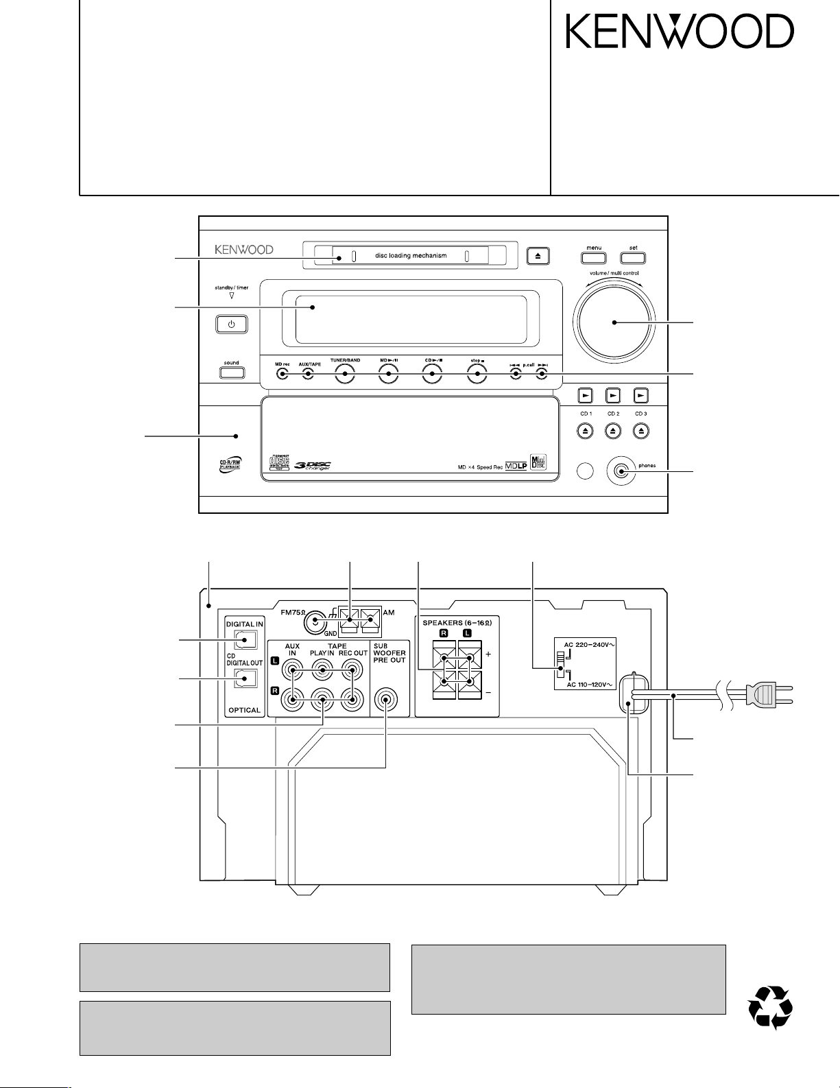
Door(MD)
(A52-0989-08)
Window *
(B10-3934-08)
Panel *
(A60-)
Cabinet *
(A01-)
Tuner *
(W02-)
SW, Push block
(E21-0041-08)
© 2002-11 PRINTED IN KOREA
B51-5835-00 (K/K) 3430
Knob(VOLUME)
(K29-8275-08)
Button
(K29-8274-08)
Jack,D3.5
(E11-0969-08)
SW, Slide *
(S62-0098-08)
Module
(W02-2802-05)
Module
(W02-2803-05)
Ter,RCA
(E63-0187-08)
Ter,RCA
(E63-1181-08)
In compliance with Federal Regulations, following are reproduction of labels on, or inside the product relating to laser
product safety.
Caution : No connection of ground line if disassemble
the unit. Please connect the ground line on
rear panel, PCBs, Chassis and some others.
Cord ass'y *
(E30-)
Stopper(AC cord)
(J42-0355-08)
* Refer to parts list on page 41.
Illust. is RD-HD5MD.
KENWOOD Corp. certifies this equipment conforms to DHHS
Regulations No.21 CFR 1040. 10, Chapter 1, subchapter J.
DANGER : Laser radiation when open and interlock defeated.
AVOID DIRECT EXPOSURE TO BEAM.

RD-HD5MD/HD7
FM indoor antenna (1)
(T90-0904-08)
AM loop antenna (1)
(T90-0903-08)
Remote control unit (1)
(A70-1625-08): RD-HD5MD(T)
(A70-1626-08): RD-HD5MD(M), RD-HD7(V)
(A70-1629-08): RD-HD7(E,T)
(A70-1630-08): RD-HD7(K)
Batteries (R6/AA) (2)
1 Remove the CD from the unit.
2 Press the CD 6 key.
3 Wait for some time and verify that the dis-
play appears as above.
4 Wait a few seconds and turn the unit OFF.
Note related to transportation and
movement
Before transporting or moving this unit, carry out
the following operations.
Condensation (of dew) may occur inside the unit when
there is a great difference in temperature between this
unit and the outside.
This unit may not function properly if condensation occurs. In this case, leave the unit for a few hours and
restart the operation after the condensation has dried
up.
Be specially cautious against condensation in a following circumstances:
When this unit is carried from one place to another
across a large difference in temperature, when the humidity in the room where this unit is installed increases,
etc.
Caution on condensation
Memory backup function
Stored contents which are cleared immediately
when power plug is unplugged from power outlet :
Clock display
N.B. function
Stored contents which will back-up after power
plug is unplugged from power outlet:
State of power (on or standby), A, P, S, Last input
selection, AUX level, Volume control value, Balance
control, Receiving band, Frequency, Preset station,
Program Timer, TONE
Operation to reset
The microcomputer may fall into malfunction (impossibility to operate, erroneous display, etc.) when the power
cord is unplugged while unit is ON or due to an external
factor. In this case, execute the following procedure to
reset the microcomputer and return it to normal condition.
Unplug the power cord from the power outlet, then while
holding the set key on the main unit depressed, plug the power
cord again.
÷ Please note that resetting the microcomputer clears
the contents stored in and it returns to condition
when it left the factory.
CONTENTS / ACCESSORIES / CAUTIONS
Contents
CONTENTS / ACCESSORIES / CAUTIONS............. 2
EXTERNAL VIEW .......................................................3
DISASSEMBLY FOR REPAIR / ADJUSTMENT.........4
CIRCUIT DESCRIPTION ............................................5
PC BOARD .............................................................. 18
Accessories
SCHEMATIC DIAGRAM .......................................... 24
EXPLODED VIEW ....................................................36
PARTS LIST..............................................................41
SPECIFICATIONS ....................................................51
Cautions
2
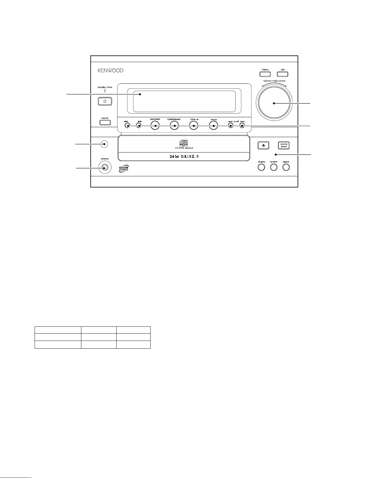
Window *
(B10-)
RD-HD5MD/HD7
EXTERNAL VIEW
Knob *
(K29-)
Window
(B11-1573-08)
Phone jack
(E11-0969-08)
tuning
Knob *
(K29-8274-08)
Front panel *
(A60-)
* Refer to parts list on page 41.
Illust. is RD-HD7.
SYSTEM CONFIGURATION
SYSTEM NAME RECEIVER SPEAKER
HD-5MD RD-HD5MD LS-HD7
HD-7 RD-HD7 LS-HD7
3
RD-HD5MD/HD7
No.
ITEM
INPUT
SETTINGS
OUTPUT
SETTINGS
RECEIVER
SETTINGS
ALIGNMENT
POINTS
ALIGN FOR
FIG.
AUDIO SECTION : SELECTOR : EXCEPT TUNER MODE
<1>
IDLE CURRENT
(RD-HD7 only)
Connect a DC
voltmeter to
CP901 or CP902
CP901 (Lch)
CP902 (Rch)
Volume:
Minimum
VR203 (Lch)
VR204 (Rch)
8 mV
DISASSEMBLY FOR REPAIR / ADJUSTMENT
DISASSEMBLY FOR REPAIR
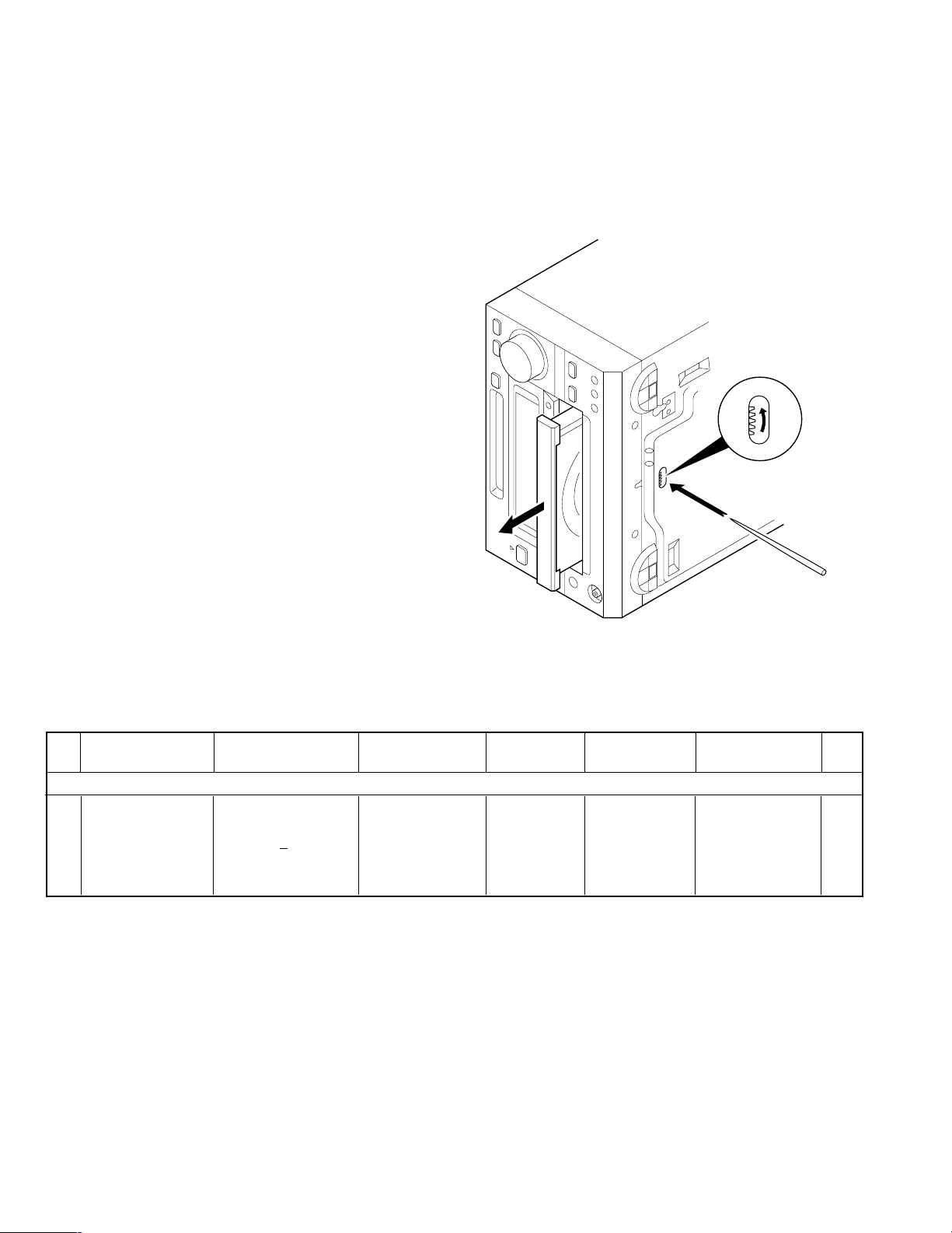
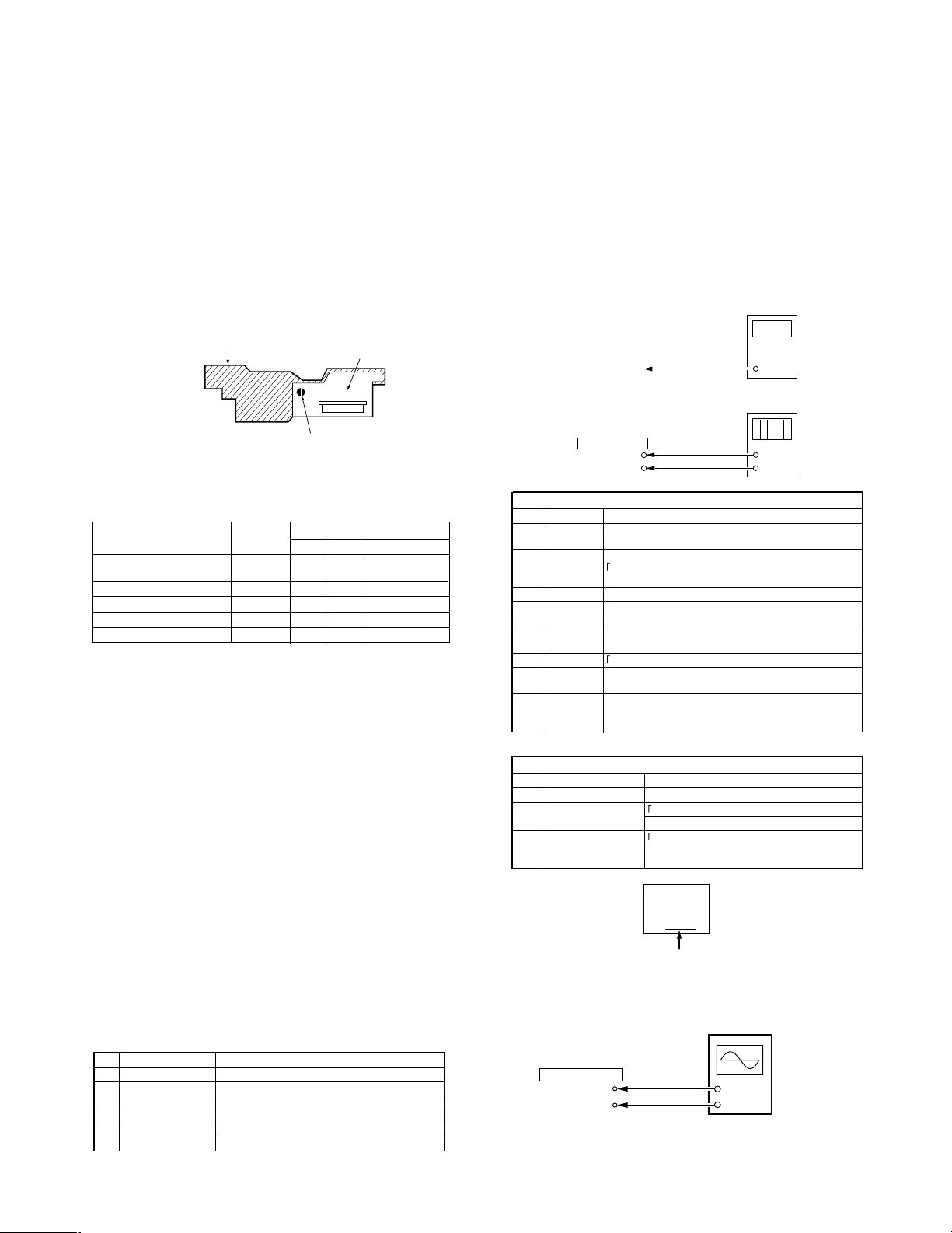
How to open the tray if it does not come out.
1. Turn the gear in the direction of the arrow using a bamboo stick and so on in the drawing through the hole on the loading chassis
bottom.
Note : Do not use a screw driver like a metallic instead of a bamboo stick.
(There is a danger of damaging the gear.)
2. Pull out the tray frontward by hand when it comes just out.
ADJUSTMENT
4
RD-HD5MD/HD7
(1) Setting of Continuous Playback Mode
No. Key Display/Function
1 VOLUME Select CREC-PLAY
2
Load a recordable disc.
3 (MD)6
(MD)6
CREC (ZZZZ) (CREC address)
0300h cluster = recording start point
ó
CPLAY ?
4 CPLAY MID
C = XXXX a = YY (error)
C1 error ADIP error
address MID = 0300h cluster
5 STOP
CREC-PLAY
ó
(1) Setting of Continuous Recording Mode
No. Key Display/Function
1 VOLUME Select CREC-PLAY
2
Load a recordable disc.
3 (MD) CREC (ZZZZ) (CREC address)
0300h cluster = recording start point
CPLAY ?
4 STOP CREC-PLAY
6
CIRCUIT DESCRIPTION
1. Initializing
1-1 Initializing Method
• While holding down the [SET] key, plugged in the
power cord to AC power wall outlet.
1-2 Initializing Operation
• During the initial operation, the display shows "INITIAL-
IZE "and after that it will be returned to standby condition.
2. Test Mode
2-1 Setting method of the Test Mode
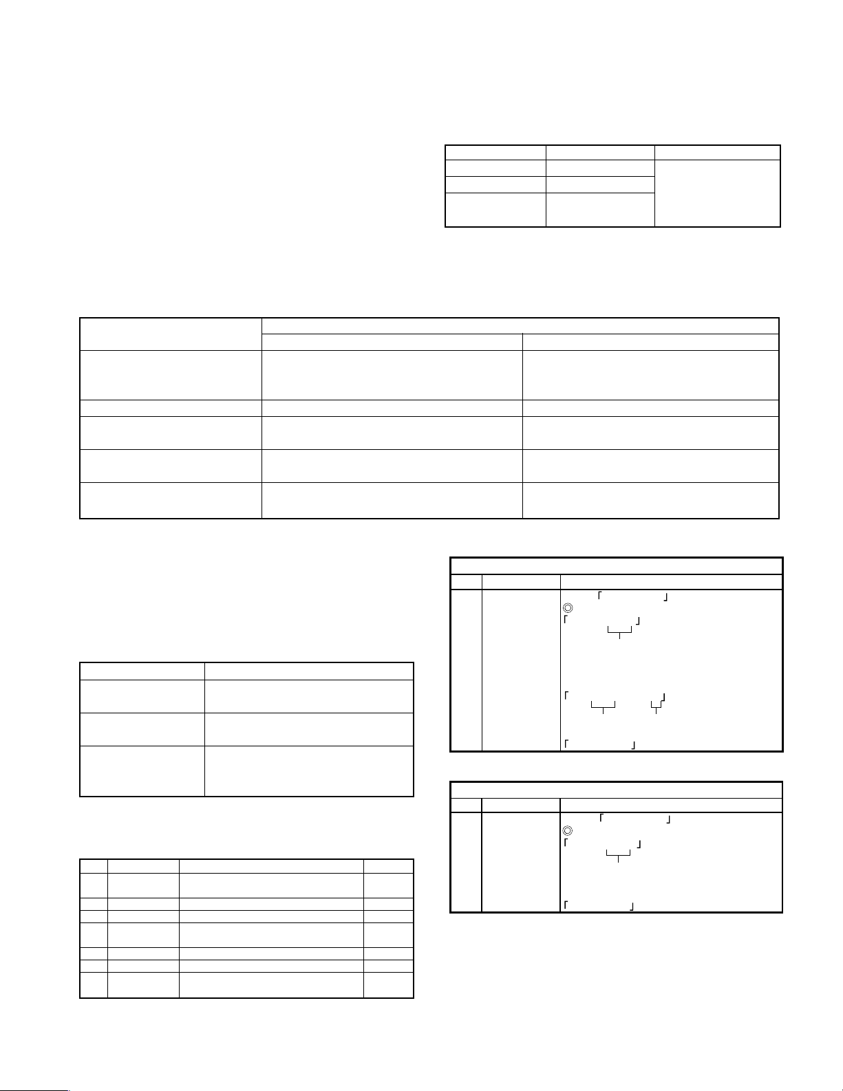
Test Mode Keys Setting Method
CD Test Mode CD PLAY PAUSE Insert the AC cord to
MD Test Mode MD PLAY PAUSE AC wall outlet while
MD Mecha. Test MD REC holding down
Mode the left key.
2-2 Cancel of the test mode
• Initialized and cancel the test mode if pulling out the power cord.
2-3 Operation of the Test Mode
Key
CD Test Mode MD Test Mode
CD-PLAY/PAUSE
(cyclically change the mode Tracking-Servo ON/OFF -
05 and 03 by pressing the key.
MENU CD double speed CD normal speed -
P.CALL UP
P.CALL DOWN
• CD Track number up
•The pickup travels outward in the stop mode.
• CD Track number down
• The pickup travels inward in the stop mode.
SET -
Operation
MD Track number up
MD Track number down
Stop the MD operation, and start the ALLERASE operation if the disc is recordable.
3. MD Test Mode for Adjustment
3-1 Contents of the Test Mode 3-2 Entering the Test Mode
• Turn the AC on while pressing the MD[REC] key.
3-3 Canceling the Test Mode
• Turn the AC off.
3-4 Key Operations for Adjustment
KEYS OPERATION
Volume/multi-control Select the mode or changed
the adjustment value.
MD PLAY/PAUSE
STOP
3-5 Selection of Adjustment Test Mode
• Whenever the [volume/multi-control] knob is turned the
adjustment test mode is selected.
No. LCD DESCRIPTION SECTION
1 TEMP ADJU
2 LDPWR ADJU Laser power adjustment. 4-6
3 LDPWR CHEC Laser power check. 4-6
4 EFBAL ADJU
5 TE B. ADJ Automatic EF balance adjustment. 4-8
6 FBIAS ADJU Focus bias adjustment. 4-9
7 CREC-PLAY Continuous recording mode. 3-7
For more information on each adjustment mode, refer to
each section of 4, "Electrical adjustment".
Fix the mode or adjustment value.
Skip to next step.
Cancel the selected mode and
changed to menu page.
Return to the state previous before.
The work of adjustment is unnecessary
in this mode.
EF balance adjustment
(Traverse adjustment).
Continuous playback mode. 3-6
4-5
4-7
3-6 Continuous Playback Mode
3-7 Continuous Recording Mode
4. Electrical adjustment
4-1 Precaution during confirmation of Laser Diode
emission
During adjustment, do not view the emission of a laser
diode from just above for confirmation. This may damage your eyes.
5
RD-HD5MD/HD7
TE1
VC
Oscilloscope
X33
ADJUSTMENT
+
-
V: 0.5V/div H: 10ms/div
INPUT: DC mode
Pick-up
Flexible board
Laser tap
No.
Key Display/Function
1
Volume/multi-control
Select [TEMP ADJU]
2 PLAY [TEMP=xx (yy)]
(xx=compensation data, yy=setting temperature)
3
Volume/multi-control
Input "yy" with present temp..
4 PLAY [TEMP=✽✽SA]
[TEMP ADJU] in writing data
+
-
Laser
power meter
Digital
voltmeter
Objective lens of
optical pick up
TP2
TP1
X33
ADJUSTMENT
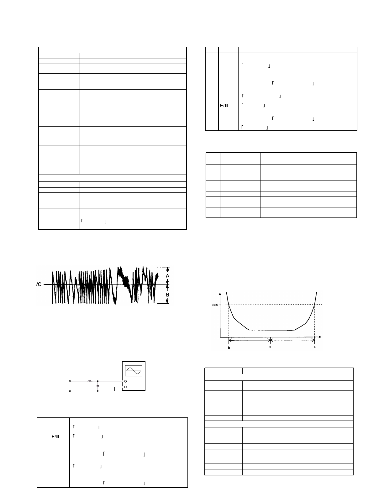
1. Laser Power Adjustment
No. Key Display/Function
1
Volume/
multi-control
[LDPWR ADJU]
Load recordable disc
2 Load the disc and lazer on
a 0.9mW) $xx] read power
(xx=power value)
3 EJECT
PLAY
Unload the disc and laser on
4 4/¢ Move the pickup to check the laser power with
laser power meter sensor
5
Volume/
multi-control
Adjust "xx" so that the power meter shows 0.9mW.
6 PLAY a 7.0mW) $xx] writing power
7
Volume/
multi-control
Adjust "xx" so that the power meter shows 7.0mW.
This adjustment should be carried out in 15 secs.
8 PLAY Laser power off
Display shows [LDPWR ADJU] after [LDPWR<$xx]
to save the data in E2PROM
Start from No.2 if readjust.
2. Laser Power Check
No. Key Display/Function
1
Volume/multi-control
[LDPWR CHEC]
2 PLAY c 0.9mW) $xx]
(xx=0.85 to 0.95mW)
3 PLAY c 7.0mW) $xx]
Laser power meter: 7.0±1.0mW✽
VOM:optical pickup indication value ±10%✽
In this case, lop = 82.5 mA
lop(mA) = Reading of digital voltmeter(mV)/1(Ω)
(optical pick-up label)
KMS
260B
27x40
B0825
CIRCUIT DESCRIPTION
4-2 Precaution on handling of Optical pick-up
(KMS-260B)
The laser diode in an optical pick-up is easy to be subject to electrostatic destruction. Therefore, solder-bridge
the laser tap on the flexible board when handling the
optical pick-up.
When removing the flexible board from the connector,
make a solder bridge in advance, then remove the board.
Be careful not to remove the solder bridge before inserting the connector. Moreover, take careful measures
against electrostatic destruction. The flexible board is cut
easily. Handle the flexible board with care.
4-3 Precaution during adjustment
1) Perform the adjustment and confirmation marked with “O”
in the order shown in the table when the parts below are
replaced.
Optical BD board
1.Temperature compensation offset adjustment X O O O
2.Laser power adjustment O O X O
3.Traverse adjustment O O X O
4.Focus bias adjustment O O X O
5.Error rate confirmation O O X O
2) In the test mode, perform the adjustment. After adjustment is completed, cancel the test mode.
3) Perform the adjustment in the order described.
4) Use the following tools and measurement equipment.
• CD test disc TGYS-1
• Laser power meter
• Oscilloscope (with bandwidth of more than 40 MΩ)
(Calibrate the probe before measurement.)
• Digital voltmeter
• Thermometer
5) Take care that VC and GND (ground) are not connected
on the oscilloscope when two or more signals are monitored on the oscilloscope. (VC and GND are short-circuited in this case.)
4-4 Creating the recordable continuous recording
disc
This disc is used for focus bias adjustment and error rate
confirmation. How to create the recordable continuous
recording disc is 3-7.
4-5 Offset Adjustment
6
pick-up IC7 D3 IC1,IC2,IC6
4-6 Laser Power Check and Adjustment
Laser power setting in playback and recording modes.
Preparation
1. Remove the MD mechanism from the unit.
2. Connect the digital voltmeter to TP1 and TP2 on X33
pcb.
3. Remove the top plate from traverse unit.
4. Remove the magnetic head.
5. Remount the MD mechanism to the unit
4-7 EF Balance(Traverse Adjustment)
Connection :
RD-HD5MD/HD7
1. Recordable Disc
No. Key Display/Function
1 Connect the oscilloscope to TE1 and VC in X33 pcb
2
Volume/
multi-control
Select [EFBAL ADJU]
3 Load the recordable disc
4 PLAY [EFBAL MO-W]
5 PLAY [EF=$✻✻MOW]
6
Volume/
multi-control
Write power adjustment. Adjust the waveform as follows.
7 PLAY Display shows [EF=$✻✻MOR] after [EFB=✻✻xSAVE]
to save the data in E2PROM.
Mode changes write to read
Focus and disc servo are on. Tracking servo off.
8
Volume/
multi-control
Read power adjustment. Adjust the waveform as follows.
9 PLAY
Save the data in E2PROM.
Display shows [EFBAL MO-P]
PLAY
Display shows [EF=$✻✻MOP]
(Pickup travels to search pits and tune the servo to on.)
10
Volume/
multi-control
Adjust the waveform as follows.
11 PLAY Display shows[EFB=✻✻xSAVE]
to save the data in E2PROM.
Display shows [EFBAL CD] disc motor stops.
12 EJECT Unload disc.
2. Pre Master Test Disc(TGYS-1)
No. Key Display/Function
1 Load the disc(TGYS-1).
2 PLAY [EF=$✻✻CD] servo is on
3
Volume/
multi-control
Adjust the waveform as follows.
4 Save the data in E2PROM.
Display shows[EFB=✻✻xSAVE] in brief time.
EF PHASE
5 EJECT Unload disc.
No. Key Display/Function
1. CD Error Rate
1
Volume/
multi-control
[CREC-PLAY]
2 Load the test disc(TGYS-1)
3 PLAY Display shows [CPLAY MID]
Access end
[c=xxxx a=yy] xxxx=C1 error (lower 20) yy=AIDP error
4 STOP [CREC-PLAY]
5 EJECT Unload disc.
2. MO Error Rate
No. Key Display/Function
1
Volume/
multi-control
[CREC-PLAY]
2 Load the recordable disc
3 PLAY Display shows [CPLAY MID]
Access end
[c=xxxx a=yy] xxxx=C1 error (lower 50) yy=AIDP error(00)
4 STOP [CREC-PLAY]
5 EJECT Unload disc.
No. Key Display/Function
1
Volume/multi-control
Select [FBIAS ADJU]
2 Load the disc.
3 PLAY [a=xx yyyy/] point a
(xx=focus bias, yyyy=C1error)
4
Volume/multi-control
Adjust "yyyy" to 220
✻
5 PLAY [b=xx yyyy/] point b
6
Volume/multi-control
Adjust "yyyy" to 220
✻
7 PLAY [xx yyyy/] point c
Check "yyyy" within 50
8 PLAY Display shows [aa bb cc(xx)] focus bias adjust
(aa= point a,bb=b,cc=c )
(TE1)
330kΩ
10pF
(VC)
Oscilloscope
+
-
No. Key Display/Function
1 Volume
TE B. ADJ
2 Load a recordable disc.
=Low Reflection • Groove
3 TE B. MO-W (Automatic Adjustment Mode Indication)
• Writing Power
Automatic Adjustment
4 Display shows
EFB = XXX SAVE in brief time and
Next step
save the data in E2PROM.
5
TE B. MO-R (Automatic Adjustment Mode Indication)
• Reading Power
=Low Reflection • Groove
Automatic Adjustment
6 Display shows
EFB = XXX SAVE in brief time and
MD
No. Key Display/Function
Next step
7
TE B. MO-P (Automatic Adjustment Mode Indication)
• Reading Power
=Low Reflection • PIT
Automatic Adjustment
8 Display shows
EFB = XXX SAVE in brief time and
Next step
save the data in E2PROM.
9
EFBAL CHANGE (Unload a disc)
0 Load a pre-master test disc(TGYS-1).
-
MD TE B. CD (Automatic Adjustment Mode Indication)
• Reading Power
=High Reflection • PIT
= Display shows
save the data in E2PROM.
EFB = XXX SAVE in brief time and
EF PHASE menu
save the data in E2PROM.
CIRCUIT DESCRIPTION
4-9 Focus Bias Adjustment
Use the special disc(continuous recorded disc)
During this adjustment, the oscilloscope changes in units of
about 2%. Adjust so that the waveform comes nearest to the
specified value. (MO groove read power traverse adjustment)
(Traverse waveform)
Specification : A = B
Notes :
1. Data is erased during MO write when a recorded disc is
used for this adjustment.
2. If the traverse waveform is difficult to be monitored, connect an oscilloscope as shown in the figure below.
4-8 Automatic EF Balance Adjustment
• Automatic EF balance adjustment is performed.
* Notes :
1. The relation between the C1 error and focus bias value
is shown in the figure below. Points “a” and “b” in the
figure are detected by the above adjustment. Focal
position “C” is automatically obtained from points “a”
and “b” by calculation.
2. The C1 error rate fluctuates. Therefore, perform the
adjustment according to the observed mean value.
C1 error
Focus bias value
4-10 Error Rate Check
7
RD-HD5MD/HD7
CIRCUIT DESCRIPTION
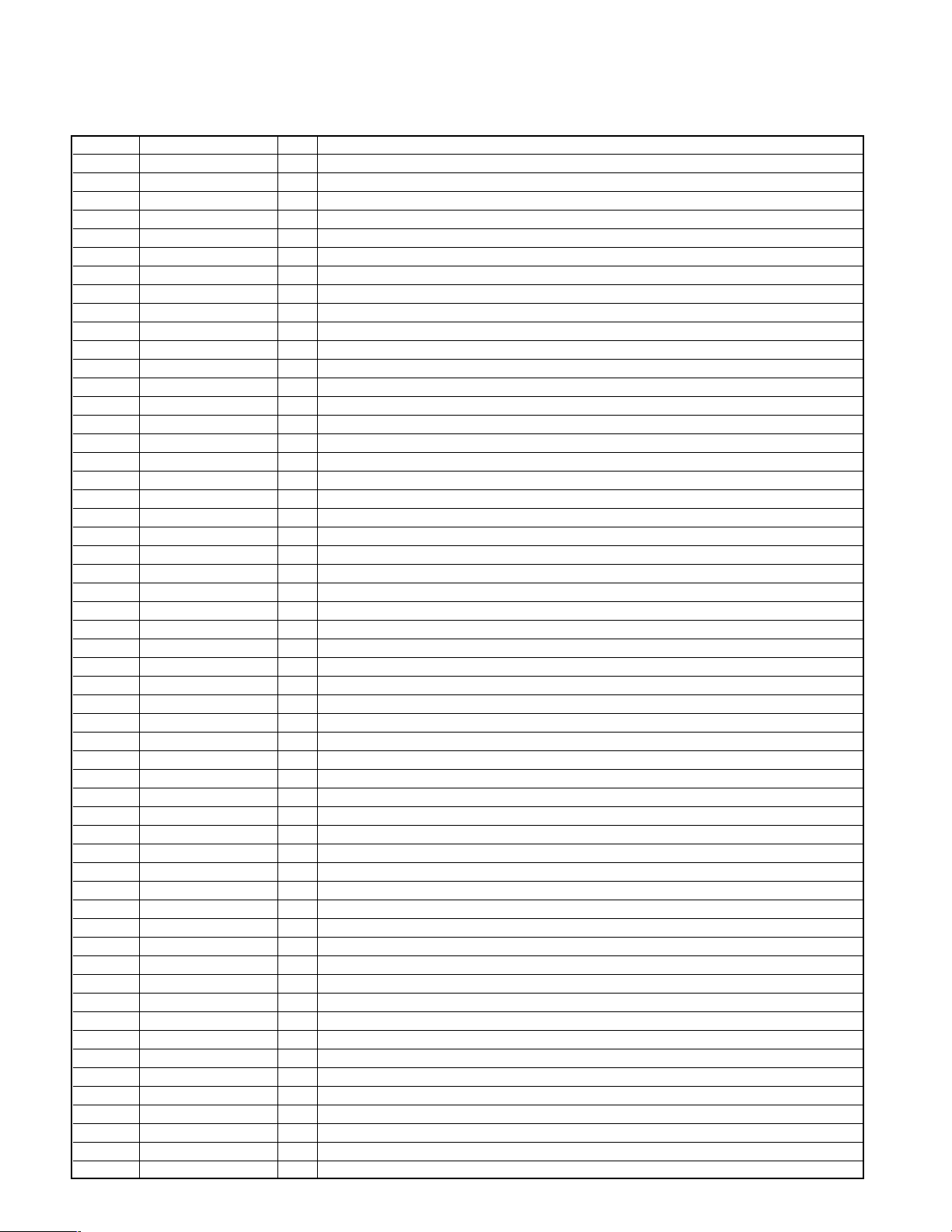
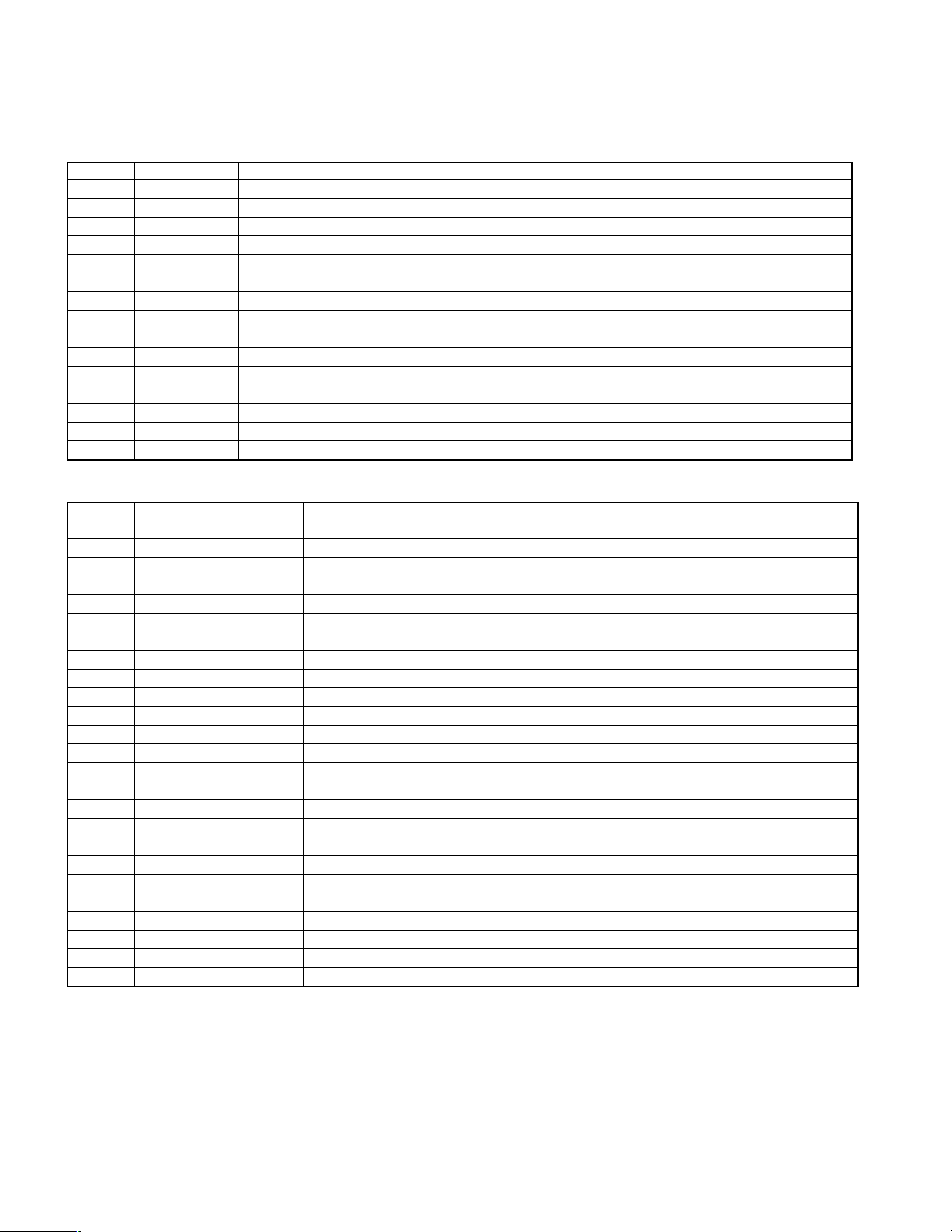
5. Pin Description of Microprocessor
Pin No. Pin Name I/O Pin Description
1 PLL DATA O Data output to PLL IC.
2 PLL CLK O Clock output to PLL IC.
3 FAN CONTROL - Unused.
4 SYS DATA O Data output to M61510FP (IC204) and M62429P (IC203).
5 M61510FP CLK O Data output to M61510FP (IC204).
6 M62429P CLK O Clock output to M62429P (IC203).
7 CE I Detection port of AC off.
8 BYTE - Connected to ground.
9 CNVSS - Connected to ground.
10 XCIN I Clock input (32.768kHz).
11 XCOUT O Clock output (32.768kHz).
12 RESET I Reset signal input for microprocessor.
13 XOUT O Main clock output (1MHz).
14 VSS - Connected to ground.
15 XIN I Main clock input (1MHz).
16 VCC - Power supply.
17 NMI - Connected to VCC.
18 REMOCON IN I Input port of remote control signal.
19 RDS CLK I RDS clock input (E/T type only).
20 BL KCK I Clock signal (88.2kHz) output.
21 PLL H/L O Switching port of reference current for CD DSP.
22 STEREO I Stereo signal input of tuner.
23 SD I Detection terminal of SD signal for TUNER.
24 LIMIT I Detection port of CD limit switch.
25 CD D. ON - Unused.
26 MLD O Command load signal output to CD DSP.
27 RDS DATA I RDS data input (E/T type only).
28 CD SPEED O Play back output port of hi-speed for CD.
29 MD RX I Data input from MD mechanism microprocessor.
30 MD TX O Transmission data output to MD mechanism microprocessor.
31 FLT DATA O Data output to FL driver.
32 RXD I Data input from EEPROM writer.
33 FLT CLK O Clock output to FL driver.
34 FLT CS O CS output to FL driver.
35 M DATA O Command data output to CD DSP.
36 STAT I Status signal input from CD DSP.
37 MLCK O Command clock signal output to CD DSP.
38 MD CE O CE of MD mechanism .
39 MD RESET O Reset signal output to MD mechanism.
40 BLUE LED CONT O Control port of blue led.
41 NC - Unused.
42 SUBQ I Data input for CD sub Q data.
43 CD SQCK O Clock output for CD sub Q data.
44 R/W SELECT I GCTL & APC control.
45 OFFTPK O Switching port of capacitance for RF bright side envelope detection.
46 FLT RESET O Reset signal output to FL driver.
47 D MUTE O Mute control for CD DSP.
48 CD LD ON O Control port of CD laser diode.
49 CD RESET O Reset output to DSP IC.
50 CD DC OFF O Power control of 4channel BTL driver.
51 DISC OPEN O Control port of CD tray motor driver.
52 DISC UP O Control port of CD lift motor driver.
53 DISC DOWN O Control port of CD lift motor driver.
54 DISC CLOSE O Control port of CD tray motor driver.
8
55 TMC O Speed control port for CD mechanism.
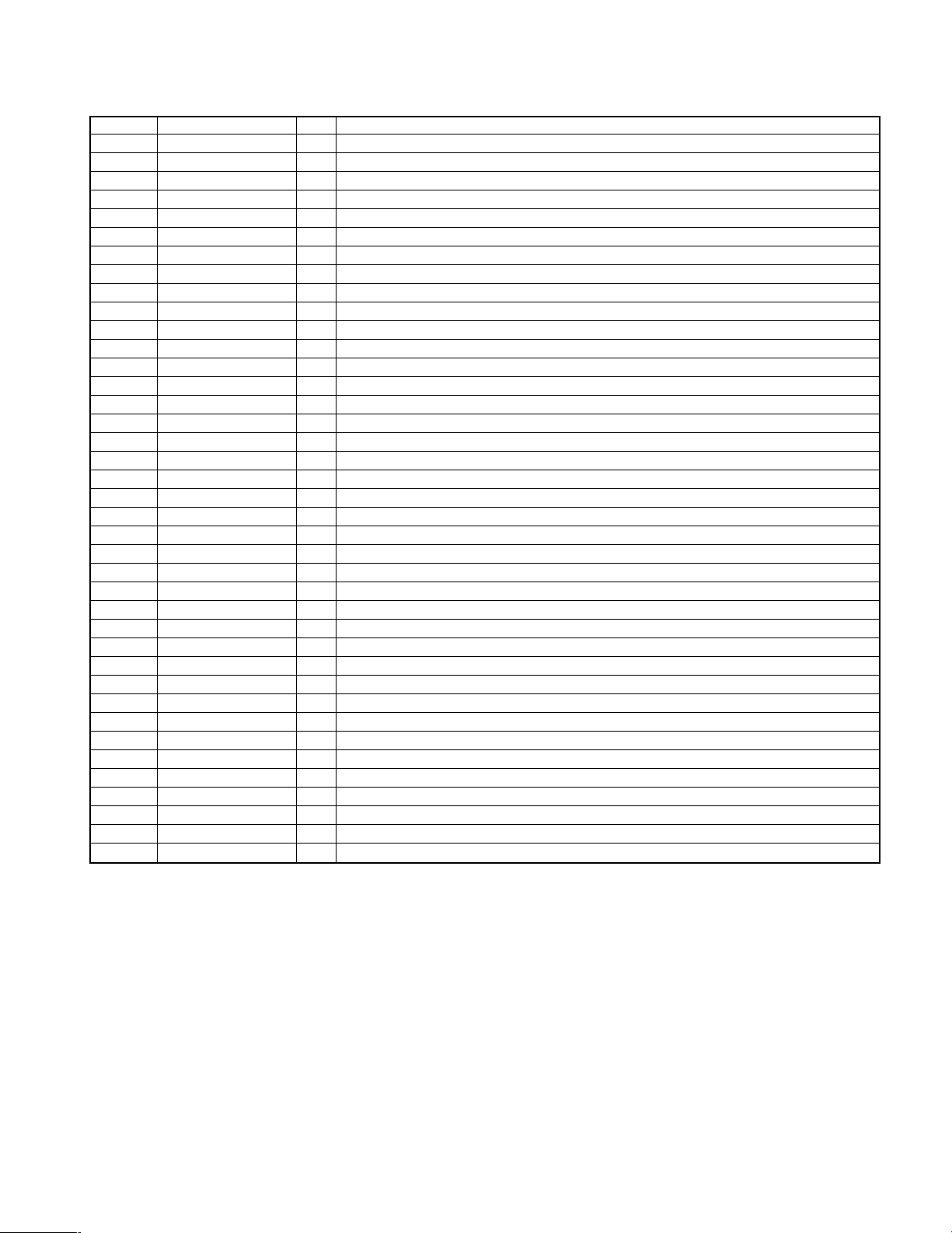
RD-HD5MD/HD7
CIRCUIT DESCRIPTION
Pin No. Pin Name I/O Pin Description
56 CD SW4 I Unclamp switch (SW4) input of CD mechanism.
57 CD SW5 I T.U High-A switch (SW5) input of CD mechanism.
58 CD SW7 I Holder Home switch (SW7) input of CD mechanism.
59 CD SW6 I T.U High-B switch (SW6) input of CD mechanism.
60 CD SW3 I Load /Clamp switch (SW3) input of CD mechanism.
61 CD SW11 I Photo2 (SW11) input of CD mechanism.
62 VCC - Power supply for microprocessor.
63 CD BOSS I Boss sensor input of CD mechanism.
64 VSS - GND
65 CD SW8 I Holder-H switch (SW8) input of CD mechanism.
66 CD SW2 I Tray Close/HP switch (SW2) input of CD mechanism.
67 CD SW1 I Tray Open switch (SW1) input of CD mechanism.
68 SENSOR I Sensor input of CD mechanism.
69 MD D. CON O Digital control port for level shift IC (IC206).
70 PROTECT2 I Detection port of protection2.
71 PROTECT1 I Detection port of protection1.
72~74 OPTION(1~3) - Unused.
75 POWER RELAY O Power relay control.
76 AMUTE O Audio mute control.
77 SP RELAY O Speaker relay control.
78~80 OPTION(4~6) - Unused.
81 MD O Mode control data output to D/A converter.
82 MC O Mode control clock output to D/A converter.
83 ML O Mode control latch output to D/A converter.
84 ST BY LED G O Timer LED (green) control terminal.
85 ST BY LED R O Standby LED (red) control terminal.
86 ENCODER A I Input port of rotary encoder (volume).
87 ENCODER B I Input port of rotary encoder (volume).
88 TU DC OFF O Power control port for tuner.
89 FAN IN I Detection port for fan level.
90~92 KEY(1~3) I Key signal inputs.
93 LEVEL L I Input port of REC amplifier.
94 LEVEL R I Input port of REC amplifier.
95 PLL CE O PLL chip enable.
96 AVSS - Analog ground.
97 N.C - Unused.
98 VREF - A/D,D/A reference voltage.
99 AVCC - Microprocessor power supply.
100 PLL DO I Input of PLL IC data.
9
RD-HD5MD/HD7
CIRCUIT DESCRIPTION
6. Pin Description of IC's
6-1 Power Amplifier : STK402 (IC1) RD-HD5MD only
Pin No. Pin Name Pin Description
1 IN1 Main Rch input
2 NF1 Main Rch feed back
3 NC Unused
4 PVCC+ Pre power supply (+B)
5 BIAS Bias connection pin
6 VE1+ Main Rch (+) output
7 VE1- Main Rch (-) output
8 VCC+ Power supply (+B)
9 VCC- Power supply (-B)
10 VE2+ Main Lch (+) output
11 VE2- Main Lch (-) output
12 PVCC- Pre power supply (-B)
13 GND GND
14 NF2 Main Lch feed back
15 IN2 Main Lch input
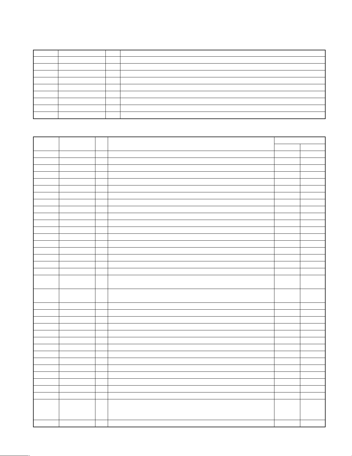
6-2 Audio Selector / E. Volume IC : M61510FP (IC204)
Pin No. Pin Name I/O Pin Description
1 REF IN I Input pin of the reference amplifier.
2 REF OUT O Output pin of the reference amplifier.
3,40 CD(L,R) I Input pin of the CD.
4,39 MD(L,R) I Input pin of the MD.
5,38 TAPE(L,R) I Input pin of the Tape play.
6,37 TUNER(L,R) I Input pin of the TUNER.
7,36 AUX(L,R) I Input pin of the AUX.
8,35 IN VOL OUT(1,2) O Output pin of the input volume 1 and 2.
9,34 IN REC-C O Output pin of the volume input selector B1and B2.
10,33 VSEL A OUT - Capacitor connection pin for the volume changing noise reduction.
11,32 LOUD(1,2) - Frequency characteristic setting pin in the loudness part.
12,31 BI(1,2) - Frequency characteristic setting pin in the tone control (Bass).
13,30 BO(1,2) - Frequency characteristic setting pin in the tone control (Bass).
14,29 MI(1,2) - Frequency characteristic setting pin in the tone control (Mid).
15,28 MO(1,2) - Frequency characteristic setting pin in the tone control (Mid).
16,27 TRE(1,2) - Frequency characteristic setting pin in the tone control (Treble).
17,26 VSEL B OUT(1,2) O Output pin of the volume input selector B1and B2.
18,25 VOL IN(1,2) I Input pin of the main volume.
19,24 VOL OUT(1,2) O Output pin of the main volume.
20 VCC - Power supply (+5.0V)
21 DATA I Input pin of the serial data.
22 CLK I Clock input.
23 GND - GND
41 REC-B2 O REC-B2 output.
42 REC-B1 O REC-B1 output.
10
RD-HD5MD/HD7
CIRCUIT DESCRIPTION
6-3 Rec Amplifier : BA6138 (IC205)
Pin No. Pin Name I/O Pin Description
1 MUTE - Mute control pin(Unused)
2 OUT1 O L ch output
3 DET1 - Unused
4 IN1 I Input of REC output (L ch)
5 GND - GND
6 IN2 I Input of REC output (R ch)
7 DET2 - Unused
8 OUT2 O R ch output
9 VCC - Power supply (+5.0V)
6-4 DSP IC : MN6627482WB( IC502)
Pin No. Pin Name I/O Pin Description
1 BCLK O Bit clock output for SRDATA.
2 LRCK O L, R clock signal output.
3 SRDATA O Serial data output.
4 DVDD1 - Digital power supply.
5 DVSS1 - Digital ground.
6 TX O Digital audio interface signal output.
7 MCLK I CPC command clock signal input.
8 MDATA I CPU command data signal input.
9 MLD I CPU command load signal input. Load
10 SENSE O Sense signal output(OFT, FESL, NACEND, NAJEND, SFG).
11 FLOCK O Focus servo signal output.
12 TLOCK O Tracking servo signal output.
13 BLKCK O Sub code block clock output. fBLKCK = 75Hz
14 SQCK I Sub code Q data clock input pin.
15 SUBQ O Sub code Q data signal output pin..
16 DMUTE I Connected to be ground. Mute
17 STAT O Status signal output.
18 RST I Reset signal input. Reset
19 SMCK O
20 PMCK O
21 TRV O Traverse forced feed output.
22 TVD O Traverse drive output.
23 PC O Spindle motor on signal output. L : ON (Default)
24 ECM O Drive signal output for spindle motor (forced mode output).
25 ECS O Drive signal output for spindle motor (servo error signal output).
26 KICK O Kick pulse output for tracking driver.
27 TRD O Tracking servo drive output.
28 FOD O Focus drive output.
29 VREF I Reference power supply for DA output section.
30 FBAL O Focus balance adjusting output.
31 TBAL O Tracking balance adjusting output.
32 FE I Focus error signal input (analog input).
33 TE I Tracking error signal input (analog input).
34 RFENV I RF envelope signal input (analog input).
35 VDET I/O Software vibrating detection monitor output when command is Detected
36 OFT I Off track signal input. Off Track
8.4672MHz clock signal output when MSEL is H.
4.2336MHz clock signal output when MSEL is L.
88.2kHz clock signal output when default.
Play signal output when command is carry out.
Vibrating detection signal input when default.
executed.
Active
HL
Play
11
RD-HD5MD/HD7
CIRCUIT DESCRIPTION
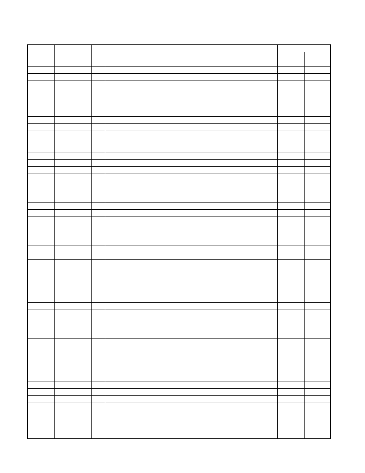
Pin No. Pin Name I/O Pin Description
37 TRCRS I Track cross signal input pin (analog input).
38 RFDET I RF detector signal input pin. Detected
39 BDO I Drop out signal input. Drop Out
40 LDON O Laser on signal output. ON
41 PLLF2 I/O PLL loop filter switching pin.
42 TOFS O Tracking offset adjusting output.
43 WVEL O Double speed status signal output.
44 ARF I RF signal input.
45 IREF I Reference current input pin.
46 DRF I DSL bias pin.
47 DSLF I/O DSL loop filter pin.
48 PLLF I/O PLL loop filter pin.
49 VCOF I/O VCO loop filter pin.
50 AVDD2 - Analog power supply for DSL, PLL, and DA output section.
51 AVSS2 - Analog ground for DSL, PLL, and DA output section.
52 EFM/CK384 O
53 PCK/DSLB O PLL clock output (fPCK = 4.3218MHz) or DSL balance output.
54 VCOF2 I/O Jitter free VCO loop filter pin.
55 SUBC O Sub code serial output.
56 SBCK I Clock input for sub code serial output.
57 VSS - GND
58 X1 I Crystal oscillation circuit input. f =16.9344MHz, 33.8688MHz
59 X2 O Crystal oscillation circuit output. f =16.9344MHz, 33.8688MHz
60 VDD - Power supply for crystal oscillation circuit.
61 BYTCK O
62 CLDCK O Sub code frame clock signal output (fCLDCK = 7.35kHz) when
63 FCLK O Crystal frame clock signal output (fFCLK = 7.35kHz) when
64 IPFLAG O Interpolation flag signal output.
65 FLAG O Flag signal output.
66 CLVS O Spindle servo phase synchronism signal output. CLV
67 CRC O Sub code CRC checked output. OK NG
68 DEMPH O De-emphasis detection signal output. ON
69 RESY O when IOSEL is H.
70 IOSEL I Switching pin for mode.
71 TEST I Test pin. Normal
72 AVDD1 - Analog power supply for audio output section.
73 OUTL O L ch audio output.
74 AVSS1 - Analog ground for audio output section.
75 OUTR O R ch audio output.
76 RSEL I RSEL is L when bright level is L.
EFM signal output when IOSEL is H.
16.9344MHz clock output when IOSEL is L.
Bite clock signal output when IOSEL is H.
Traverse stop signal output when IOSEL is L.
General IO pin when default.
command is carry out.
General IO pin when default.
command is carry out.
Re-frame synchronism signal RESY output of frame synchronism
H : Synchronized L : Non synchronized
• RF signal polarity assignment pin when default.
RSEL is H when bright level is H.
• General IO pin when command is executed.
RF signal polarity assignment is set by command.
Stop Mode
Active
HL
Double
Speed
12

RD-HD5MD/HD7
CIRCUIT DESCRIPTION
Pin No. Pin Name I/O Pin Description
77 CSEL I
78 PSEL I
79 MSEL I
80 SSEL I
6-5 D/A Converter : PCM1742 (IC507)
Pin No. Pin Name I/O Description
1 BCK I Audio data bit clock input.
2 DATA I Audio data digital input.
3 LRCK I Audio data latch enable input.
4 DGND - Digital ground.
5 VDD - Digital power supply (+3.3V).
6 VCC - Analog power supply (+5V).
7 VOUTL O Analog output for L-channel.
8 VOUTR O Analog output for R-channel.
9 AGND - Analog ground.
10 VCOM - Common voltage decoupling.
11 ZEROR O Zero flag output for R-channel.
12 ZEROL O Zero flag output for L-channel.
13 MD I Mode control data input.
14 MC I Mode control clock input.
15 ML I Mode control latch input.
16 SCK I System clock input.
Designation of oscillation frequency.
H : f = 33.8688MHz L : f = 16.9344MHz
Test pin (Normal : L ) when IOSEL is H.
SRDATA input when IOSEL is L.
SMCK output when IOSEL is H. Switching pin of frequency.
H : SMCK = 8.4672MHz L : SMCK = 4.2336MHz
LRCK input when IOSEL is L.
H : Lch data, L : Rch data SMCK = 4.2336MHz (Fixed)
SUBQ output mode switching pin when IOSEL is H.
H : Q code buffer use mode L : CLDCK synchronism mode
BCLK input when IOSEL is L.
Q code buffer use mode
Active
HL
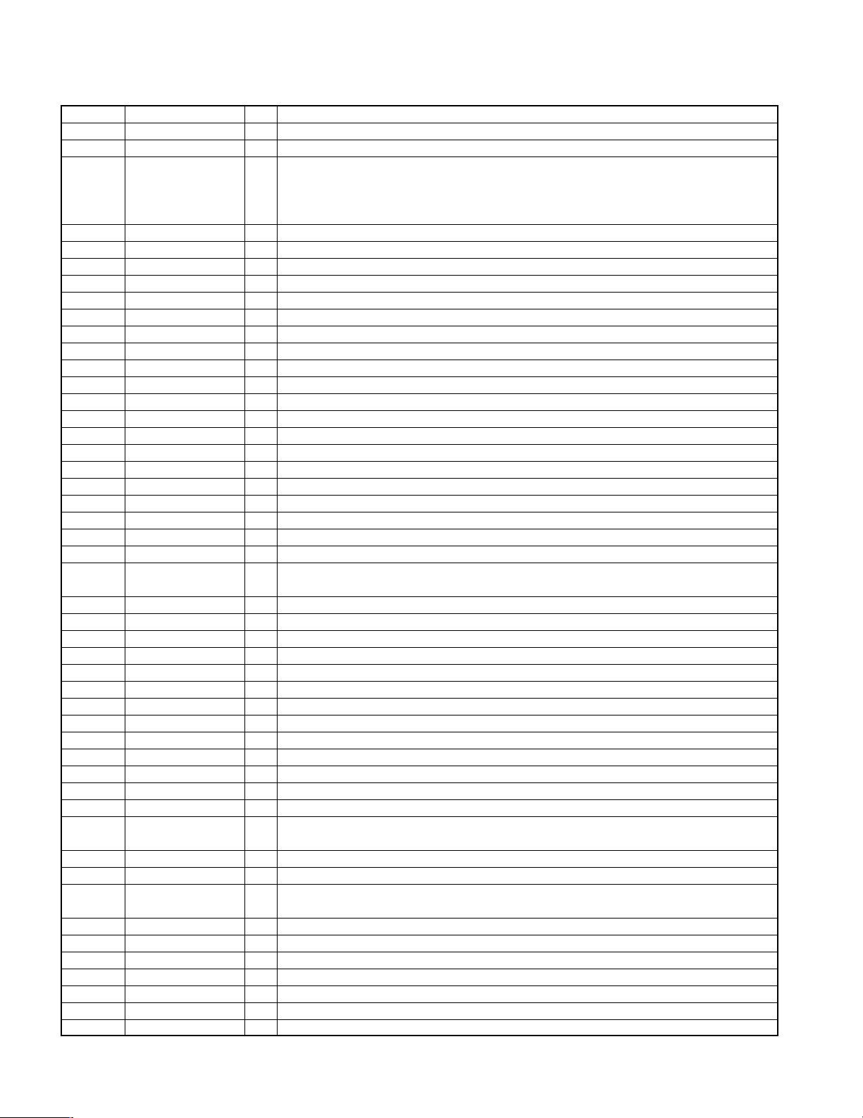
6-6 Digital Signal Processor : CXD2664R (X33, IC1)
Pin No. Pin Name I/O Pin Description
1 MNT0 I/O Monitor output.
2~4 MNT(1~3) O Monitor output.
5 VDC0 - CORE power supply.
6 SWDT - Data input for microcomputer serial interface.
7 SCLK - Shift clock input for microcomputer serial interface.
8 XLAT - Latch input for microcomputer serial interface. Latched at the falling edge.
9 VSC0 - CORE GND.
10 SRDT O Data output for microcomputer serial interface.
11 SENS O
12 XRST I Reset input. Low : reset
13 SQSY O Disc subcode Q sync/ADIP sync output.
14 DQSY O U-bit CD or MD format subcode Q sync output when the digital in source is CD or MD.
15 RPWR I Laser power switching. High : recording power, Low : playback power
16 XINT O Interrupt request output. Low when the interrupt status occurs.
17 TX I Enable signal input for recording data output. High : enable
18 VDIO0 - I/O power supply.
19 OSCI I Crystal oscillation circuit input.
20 OSCO I/O Crystal oscillation circuit output. (Input when OSCN = high.)
Outputs the internal status corresponding to the microcomputer serial
interface address.
13
RD-HD5MD/HD7
CIRCUIT DESCRIPTION
Pin No. Pin Name I/O Pin Description
21 OSCN I Control for feedback resistor and inverter inside oscillation circuit.
22 VSIO0 - I/O GND.
OSCI pin input frequency switching.
23 XTSL I
24,25 DIN (0,1) I Digital audio interface signal input (0,1).
26 DOUT O Digital audio interface signal output.
27 DATAI I 3-wire data input for recording.
28 LRCKI I 3-wire LR clock input for recording.
29 XBCKI I 3-wire bit clock input for recording.
30 VDC1 - CORE power supply.
31 VSC1 - CORE GND.
32 ADDT I Data input from A/D converter.
33 DADT O REC monitor output/decoding audio data output.
34 LRCK O LR clock output to external audio block.
35 XBCK O Bit clock output to external audio block.
36 F256 O 256Fs output.
37 XWE O External DRAM write enable output.
38 XOE O External DRAM read enable output.
39 DRVDD0 - DRAM interface power supply.
40 DRVSS0 - DRAM interface GND.
41 A11 O External DRAM address output.
42~45 D3,D0,D2,D1 I/O External DRAM data bus.
46 XCAS O External DRAM XCAS output.
47 XRAS O External DRAM XRAS output.
48~56
57 VDC2 - CORE power supply.
58 VSC2 - CORE GND.
59,60 A04,A03 O External DRAM address output.
61 DRVDD1 - DRAM interface power supply.
62 DRVSS1 - DRAM interface GND.
63,64 TEST(0,1) I Connect to the analog power supply.
65 TEST2 O No connected.
66 AVD1 - Analog power supply.
67 ASYO O Playback EFM full-swing output.
68 ASYI I Playback EFM comparator slice voltage input.
69 BIAS I Playback EFM comparator bias current input.
70 RFI I Playback EFM RF signal input.
71 AVS1 - Analog GND.
72 PCO O
73 FILI I Filter input for master PLL of playback digital PLL and recording EFM PLL.
74 FILO O Filter output for master PLL of playback digital PLL and recording EFM PLL.
75 CLTV I
76 PEAK I Peak hold signal input for quantity of light.
77 BOTM I Bottom hold signal input for quantity of light.
78 ABCD I Signal input for quantity of light.
79 FE I Focus error signal input.
80 AUX1 I Auxiliary input 1.
81 VC I Center voltage input.
82 ADIO O Test. No connected.
A09~A10,A07,A00,
A06,A01,A05,A02
512Fs (22.5792MHz) when XTSL 1 (command) =low and XTSL = high.
1024Fs (45.1584MHz) when XTSL 1 = low and XTSL = low.
2048Fs (90.3168MHz) whe
O External DRAM address output.
Phase comparison output for master PLL of playback digital PLL and
recording EFM PLL.
Internal VCO control voltage input for master PLL of playback digital PLL
and recording EFM PLL.
14
 Loading...