Kenwood RDDV-5-MDS, RDDV-5-S, RDDV-7-L Service manual
70%
MICRO HiFi COMPONENT SYSTEM
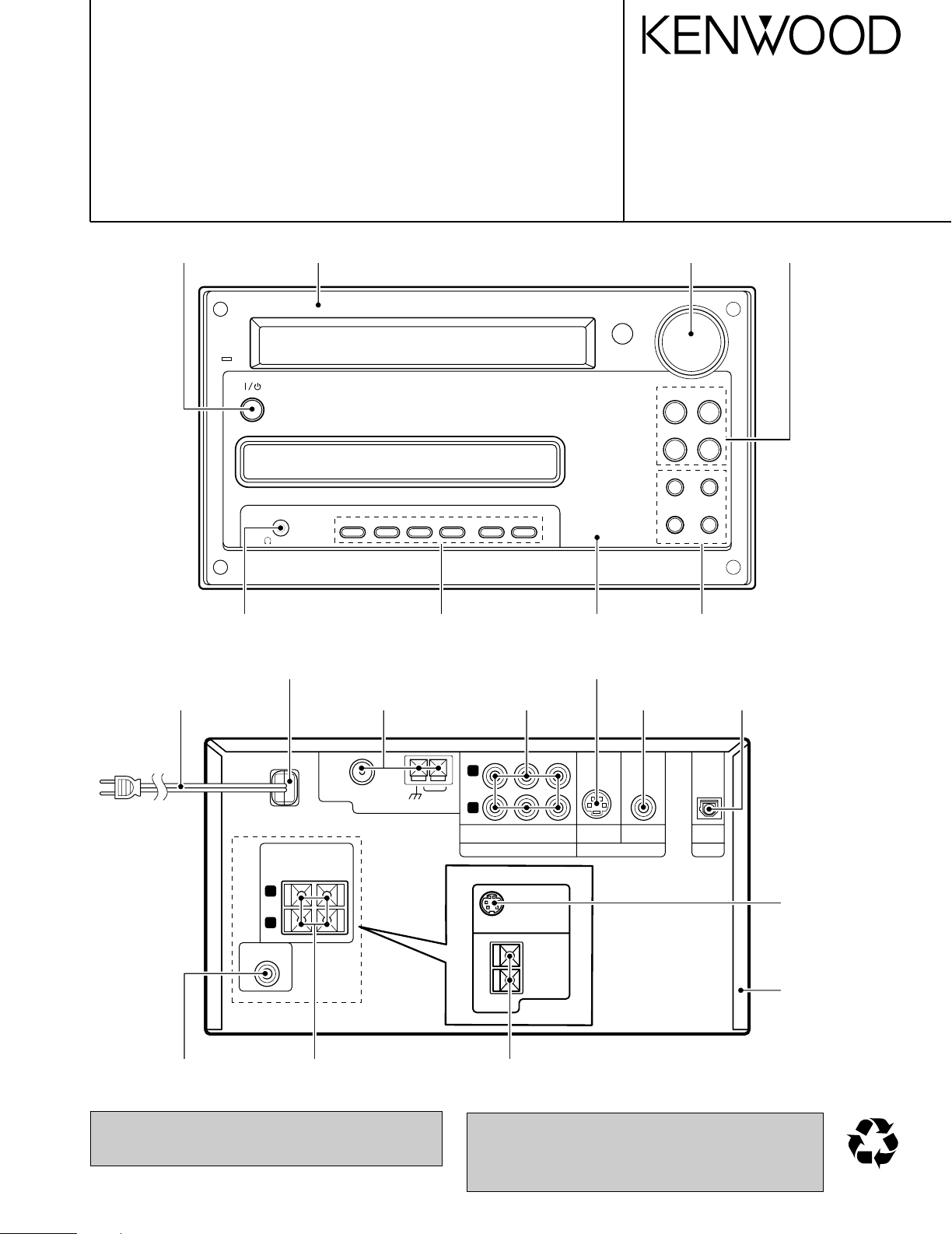
VOLUME/
MULTI CONTROL
STANDBY
/TIMER
DVD/CD 6TUNER/
BAND
41¢
¡
DVD/CD 0STOP
7
TUNING MODE
AUX
PHONES
SOUND MODE SET/DEMO REPEAT RANDOM
P.CALL
R
L
GND
FM75 Ω
AM
SUB WOOFER
PRE OUT
ANTENNA
AUDIO
AUXINCD - R
OUT
S-VIDEO VIDEO
VIDEO OUT
OPTICAL
DIGITAL OUT
PCM/BIT
STREAM
CD - R
IN
+
-
R
L
SPEAKERS
( 6
-16 Ω
)
RD-DV5
TO OPM-DV7
SATELLITE
SPEAKER
SUB
WOOFER
+
-
( 8
-16
)
Ω
RD-DV7
RD-DV5-S/DV7-L
RD-DV5MD-S
SERVICE MANUAL
Knob *
(K29-)
Phone jack
(E11-0941-05)
AC power cord bushing
(J42-0083-05)
AC power cord *
(E30-)
Panel *
(A60-)
Knob
(K29-7999-03)
Tuner assy *
(W02-)
Dressing panel *
(A21-)
Cylindrical receptacle
(E56-0032-05)
Pin jack *
(E63-)
© 2001-9 PRINTED IN KOREA
B51-5754-00 (K/K) 2345
Knob
(K29-8001-14)
Knob *
(K29-)
Pin jack
(E63-1220-05)
Knob
(K29-7997-03)
Oscillating module
(W02-2803-05)
Pin jack
(E63-1162-05)
In compliance with Federal Regulations, following are reproduction of labels on, or inside the product relating to laser
product safety.
Lock terminal board
(E70-0148-05)
Lock terminal board
(E70-0146-05)
KENWOOD-Corp. certifies this equipment conforms to DHHS
Regulations No.21 CFR 1040. 10, Chapter 1, subchapter J.
* Refer to parts list on page 48 .
Illustration is RD-DV5-S/DV7-L.
DANGER : Laser radiation when open and interlock defeated.
AVOID DIRECT EXPOSURE TO BEAM.
Cylindrical receptacle
(E56-0038-05)
Metallic cabinet
(A01-3820-11)

RD-DV5-S/DV7-L/DV5MD-S
The marking this product has been
classified as Class 1. It means that
there is no danger of hazardous radiation outside the product.
Location: Back panel
CLASS 1
LASER PRODUCT
The marking of products using lasers
(For countries other than U.S.A., U.S.-Military and Canada)
Inside this laser product, a laser diode classified as Class 2 laser radiation is contained as alerted by
the internal caution label shown
above. Do not stare into beam.
Location: DVD laser pick-up unit
cover inside this product
CAUTION
VISIBLE LASER RADIATION
WHEN OPEN. DO NOT
STARE INTO BEAM.
Inside this laser product, a laser diode classified as Class 3B laser radiation is contained as alerted by
the internal caution label shown
above. Avoid exposure to laser
beams.
Location: MD laser pick-up unit
cover inside this product
CAUTION
VISIBLE LASER
RADIATION WHEN OPEN.
AVOID EXPOSURE TO BEAM.
Operation to reset
The microcomputer may fall into malfunction (impossibility to
operate, erroneous display, etc.) when the power cord is unplugged while unit is ON or due to an external factor. In this
case, execute the following procedure to reset the microcomputer and return it to normal condition.
Unplug the power cord from the power outlet
then, while holding the STOP 7 /TUNING MODE
key depressed, plug the power cord again.
÷ Please note that resetting the microcomputer clears
the contents stored in and it returns to condition
when it left the factory.
REMOTE MODEL
MAIN UNIT DESTINATION
CONTOROLLER NAME
A70-1521-05 RC-M0513 RD-DV5MD-S M
A70-1522-05 RC-F0504E RD-DV5-S TE
A70-1524-05 RC-F0505 RD-DV7-L M2X2V2
A70-1525-05 RC-F0505E RD-DV7-L T2E2
SYSTEM MAIN UNIT DESTINATION SPEAKER SP CORD PARTS No.
HM-DV6MD RD-DV5MD-S M LS-DV6-S E30-5500-05
HM-DV5 RD-DV5-S TE LS-DV5-S E30-5941-04
HM-DV6 RD-DV5-S E LS-DV6-S E30-5500-05
HM-DV7 RD-DV7-L T2E2M2X2V2 OPM-DV7-L E30-5943-08
Remote controller
System configurations
FM indoor antenna (1)
(T90-0855-05)
AM loop antenna(1)
(T90-0852-05)
Video cord(1)
(E30-7226-05)
Speaker cord(2)
Remote control unit(1)
(A70-1521-05): M
(A70-1522-05): TE
(A70-1524-05): M2X2V2
(A70-1525-05): T2E2
Batteries (R6/AA)(2)
SCAT plug adaptor for TV(1)
(For EUROPE and U.K.)
(E69-0012-05)
Cushion for satellite speaker(4)
(W01-1178-08)
Feet for speaker(4)
(J02-0034-08)
AC Plug Adaptor (1)
(E03-0115-05)
Use to adapt the plug on the
power cord to the shape of the
wall outlet.
(Accessory only for regions where
use is necessary.)
CONTENTS / ACCESSORIES / CAUTIONS
Contents
CONTENTS / ACCESSORIES / CAUTIONS............. 2
DISASSEMBLY FOR REPAIR....................................3
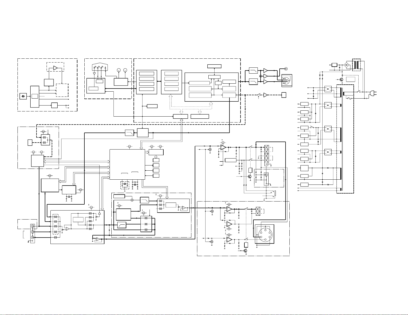
BLOCK DIAGRAM ......................................................6
CIRCUIT DESCRIPTION ............................................7
ADJUSTMENT ..........................................................14
WIRING DIAGRAM ...................................................15
Accessories
PARTS DESCRIPTIONS ..........................................16
PC BOARD .............................................................. 17
SCHEMATIC DIAGRAM .......................................... 25
EXPLODED VIEW ....................................................45
PARTS LIST..............................................................48
SPECIFICATIONS ......................................Back cover
Cautions
2
DISASSEMBLY FOR REPAIR
5cm以上
(HEX DRIVER)
2mm
2mm
GEAR
DVD(CD) MECHA
GEAR
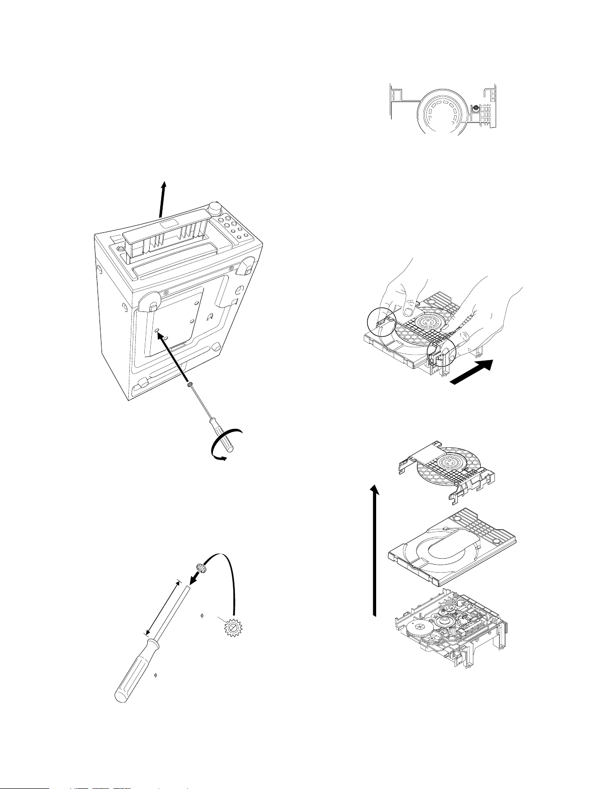
How to open the tray if it does not come out.
1. Insert a jig and turn it fully ccw in the drawing through the
hole on the loading chassis bottom.
2. Pull out the tray frontward by hand when it comes just out.
RD-DV5-S/DV7-L/DV5MD-S
Fig. 3
How to open the tray and a clamper.
1. Pull out the tray slightly frontward by hand.
(Refer to Fig .1)
2. Remove the tray.
3. Remove the clamper in the arrow direction.
Fig .1
* How to make a jig
Insert a hex wrench to a hole of gear (W05-0881-00) in
the drawing below.
If you lost the gear use it which located on DVD mechanism in the drawing (Fig .3).
Fig. 4
4. Remove the tray and clamper upward.
Fig. 5
Fig. 2
3
RD-DV5-S/DV7-L/DV5MD-S
TRAVERSE
GEAR A
GEAR B
CUT
MECHA.
CHASSIS
DISASSEMBLY FOR REPAIR
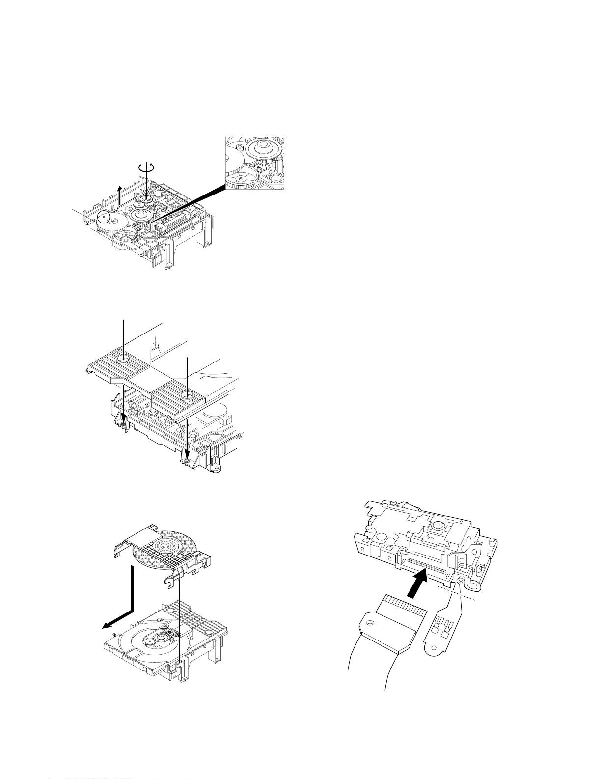
How to attach the tray and the clamper.
1. Turn the traverse gear A in the direction of the arrow in
the drawing so that the traverse
unit will reach the highest position.
Fig. 6
2. Attach the tray in the arrow direction.
Fig. 7
Assembling and Disassembling the Optical Pickup
The optical pickup can be damaged by static electricity
from your body.
Be sure to take static electricity countermeasures when
working around the optical pickup.
Handling the Optical Pickup
1. The optical pickup is an extremely high-precision mechanism. Do not subject it to strong damage.
2. Testers cannot be used to check the laser diode of the
optical pickup. The power supply in side the tester can
easily damage the laser diode.
3. Take care when handling the flexible cable because
excessive force can cause it to break.
4. To preserve the quality of the optical pickup replacement
parts during transport and installation, the terminals of the
laser diode are short-circuited. After replacing the parts,
use the proper procedure to return the laser diode to its
original condition.
Static Electricity Countermeasures
The laser diode inside the traverse unit (optical pickup )
can be damaged by static electricity from your body. Be
sure to take static electricity countermeasures when working around the optical pickup.
Static Electricity Countermeasure Methods
1. Ground yourself
Use an anti-static wrist strap to discharge static electricity
from your body.
2. Ground the workbench
Lay a conductive material (sheet) or steel sheet on the
surface where the traverse unit (optical pickup)is to be
placed, then ground the sheet.
Assembling the Optical Pickup
1. Insert a flexible cable in the arrow direction in the drawing.
2. Cut the flexible cable.
3. Attach the clamper in the arrow direction.
Fig. 8
4
RD-DV5-S/DV7-L/DV5MD-S
TILT ADJ.
SCREW 1
BOTTOM VIEW
TILT ADJ.
SCREW 2
TANGENTIAL
ADJ.SCREW
FRONT
DISASSEMBLY FOR REPAIR
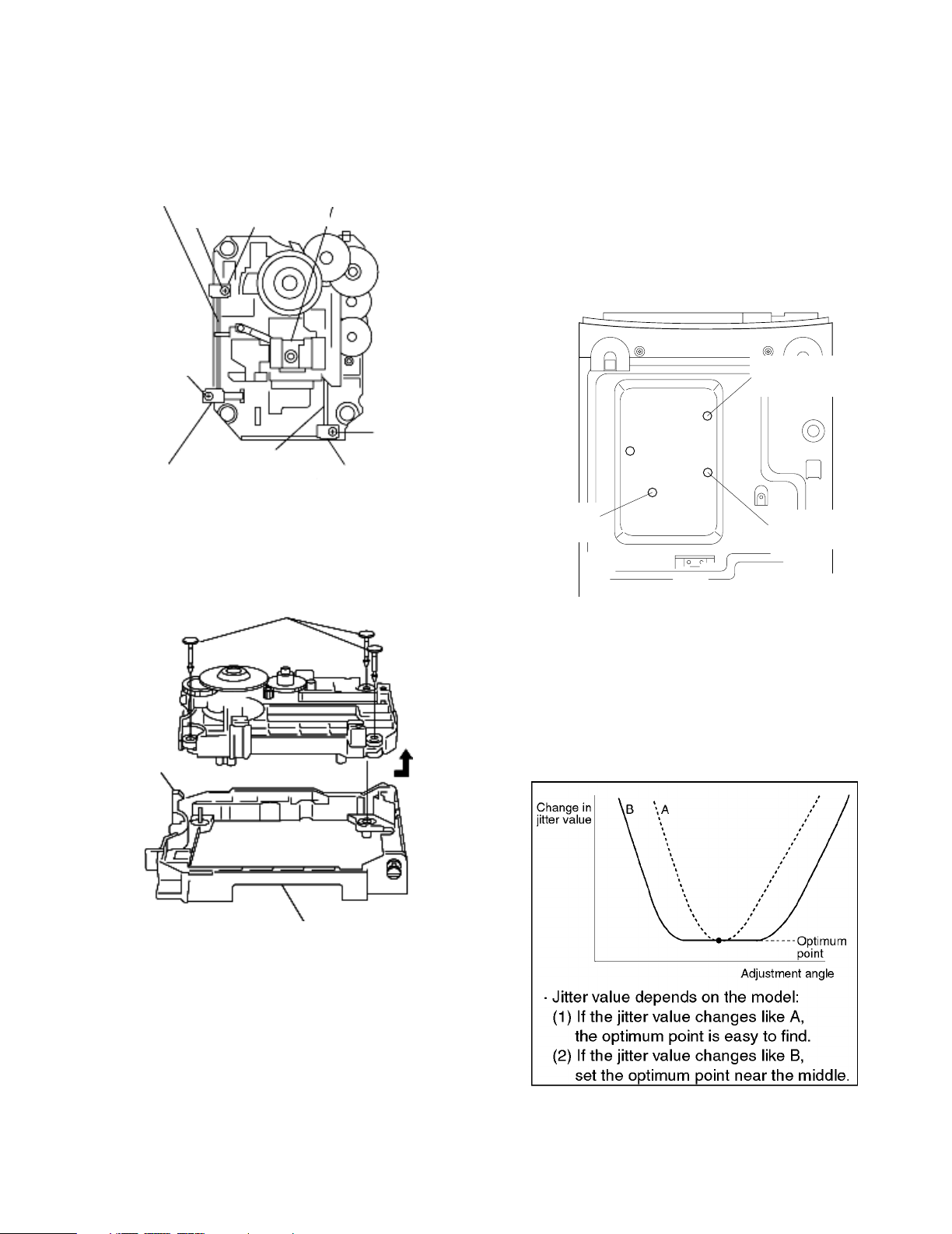
Disassembling the Optical Pickup
1. Remove screws.
2. Remove spring holder and spring.
3. Pull out the drive-shaft and guide shaft.
GUIDE SHAFT
SCREW
SCREW
SPRING HOLDER SPRING HOLDER
SPRING HOLDER
DRIVE SHFT
OPTICAL PICKUP
SCREW
Disassembling the Middle Chassis
1. Remove 3 push rivets.
2. Remove the hooks.
3. Lift the traverse unit upward to remove the middle chassis.
HOOKS
PUSH RIVETS
*6. Play DVD disc last chapter (outer periphery).
7. Adjust to the minimum jitter value.
(Tilt adjustment screw1)
*8. Play DVD disc last chapter (outer periphery).
9. Adjust to the minimum jitter value.
(Tilt adjustment screw2)
10. Repeat adjusting tilt adjustment screws 1 and 2 alternately, two or three times.
* Press "SKIP UP/SKIP DOWN" keys for Tno. up or
down.
Do item 5~10 from the bottom of the main unit using a
hex wrench.
1-2 Point
1. First of all adjust tangential adjustment then adjust tilt
adjustment.
2. To get optimum point, repeat item 1 adjustment alternately, two or three times.
3. Finally, adjust the tilt adjustment.
MIDDLE CHASSIS
1. Optical pickup Tilt Adjustment
1-1 Adjustment
1. Insert the AC power plug to AC wall outlet with pressing the DVD/CD play key.
(The tray opens automatically)
2. Load a DVD disc and press DVD/CD play key.
3. Press "SOUND" key.
(Jitter value is displayed.)
JITT XXX % XXX is present jitter value
*4. Play DVD disc first chapter (inner periphery).
5. Adjust to the minimum jitter value.
(Tangential adjustment screw)
1-3 Check condition after adjustment
1. Play the disc to make sure there is no picture degradation in the inner, middle and outer peripheries, and no
audio skipping.
2. Lock the adjustment screw in position using screw lock.
5
TRACKING
FOCUS
DVD
CD
16.9344MHz33.8688MHz
768Fs
512Fs
27MHz
384Fs
13.5MHz
ODC
ADSC
AUDIO
DAC
C
COMP
Y
+3.3V
D. IN/CD
MD D+5V MD A+3.15V
MD H+5V
ANALOG REC
PLAY
AUDIO DAC
u+5V
DVD u-COM
TUNER
RDS
XIN
L,Rch-VR
XCIN
XOUT
XCOUT
C,SWch-VR
(10MHz)
(32.768kHz)
CLOCK
COLCK
TIMMER
MAIN
-30V +5V
Lch-OUT
Rch-OUT
+9V
DET-OUT
D5V
+5V
4.332MHz
7.5V
8V
8V
C12,C34 OFF
8V
4ch
2ch
HP
C,SWch
L,Rch
B
B
MUTE
B
B
D. OUT SW
A CLASS
CONT
TH LEVEL
L,R RELAY
SP LEVEL
Cch
C,SW RELAY
SWch
+
+5.1V
POWER
RELAY
+B
++
-B
AMP
GND
AMP
+
MD HEAD.
MD
OTHER
DIGITAL
ANALOG
++
E. VOL
VIDEO
TUNER
E. VOL
DVD
+
DVD
FAN
CONT.
DVD
MOTOR
+
DRIVER
FL
+
FL
TUNER
DVD u-COM
RF AMP
AN8708
FRONT-END
PROCESSOR
EEPROM
IC201
PLL/DSL
HF
SERVO CONT
CIRC/DAC
SERVO CONTROLLER
ADVANCED DISC
AN8499
AN8708
TRAVERSE/
DRIVER
M
APC
PICKUP
LOADINGMSPDL
IC1
ECC
MN67706
MN103S13B
ATAPI
ROM DEC
IC101
OPTICAL DISC
CONTROLLER
4MDRAM
8M FLASH ROM
IC207
ADDRESS DATA BUS
AV DECODER
IC301
AC3,LPCM,MP3
AUDIO DECODER PCM &
SPDIF
SDRAM I/F
64M SDRAM
CSS DISSCRAMBLE
VIDEO DECODER
MPEG,SUB PICTURE
VIDEO DAC
ENCODER
NTSC/PAL
OSD
MN677533MP
IC401
AVDEC
IC207
1/2
SM8703AV
PLL
X202
27MHz
IC211
IC210
IC213
1/2
DVD u-COM
IC201
GENERATOR
CLOCK
S OUT
COMPOSIT
6.75MHz
6.75MHz
X29,J2
OUT
OPT OUT
X29,A2
X29,J1
X29,IC7
VIDEO
AMP
X29,IC5
X29,A1
OPT IN
MD MECHA
MDM-15AL
X29,IC5
96k 24bit
2ch DAC
X29,IC17
PCM1748
60kHz
M30624MGA356F
MAIN u-COM
X29,IC15
FL DRIVER
M66005-001FP
FL
LED
KEY
REM
X14,IC1
X14,ED1
TUNER PACK
RDS IC
X29,IC16
IN
OUT
VIDEO2
IN
VIDEO1
(AUDIO)
X29,J3
X29,IC1
M62492FP
TONE
EX. BASS
INPUT
MAIN
REC
OUT
VOL.
VOL.
ATT.
PSS-3200
A3
OTHER ch
IC3
IC4
TONE
EX. BASS
C,SW VR
PROCESSOR
STEREO AUDIO
DIGITAL CONTROLLED
TC9215AP
PAROUND
PROCESSOR
MODULE
AUDIO SEL.
POINT SOURCE
X07,J3
SATELLITE
SPEAKER
E. VOLUME
Rch
Lch
J1
S. W. PRE-OUT
X14,J1
H. P.
K2
OTHER ch
AMP
X07,IC1
Q1,2
MUTE
J4
SWch
K3
IC2
AMP
Q3
MUTE
AMP
MUTE
Q5
AMP
IC3
K3
+5V
IC11
u-COM
R/C SENSOR
R/C VDD
D10
X07,
Q302
X07,D1
S1
S2
X07,D4
+3.15V
+5V
X07,IC14
X29,IC12
POWER
RELAY
X07,D3
-8V
+8V
X29,IC11
X29,IC14
+9V
X29,IC10
S3
S4
X07,D2
X07,Q311
+3.3V
X07,IC13
+5V
X07,Q13
FAN
DRIVE
S5
X07,IC12
+9V
-30V
X07,Q14
S6
K1
PICKUP UNIT(X35-2302-72)
CLK SYSTEM
(X35-2302-72)
RD-DV5MD
ONLY
E/T ONLY
RD-DV5/DV7
ONLY
RD-DV7
ONLY
RD-DV5/
ONLY
RD-DV7
ONLY
DV5MD
RD-DV5MD/DV5/DV7
6
RD-DV5-S/DV7-L/DV5MD-S
BLOCK DIAGRAM
RD-DV5-S/DV7-L/DV5MD-S
CIRCUIT DESCRIPTION
1. Initializing
1-1 Initialization Method
• While pressing the [STOP] key, turn the AC on.
1-2 Initialization Operation
• During the initial operation, the display shows "INITIALIZE"and after that it will be returned to standby condition.
• If any mechanisms error occurred, the error indication is
displayed as "ERR" on the display.
1-3 Mechanism Initializations
DVD Mechanism
• If a mechanism error occurred, the error indication is displayed as "DVD ERR" on the display.
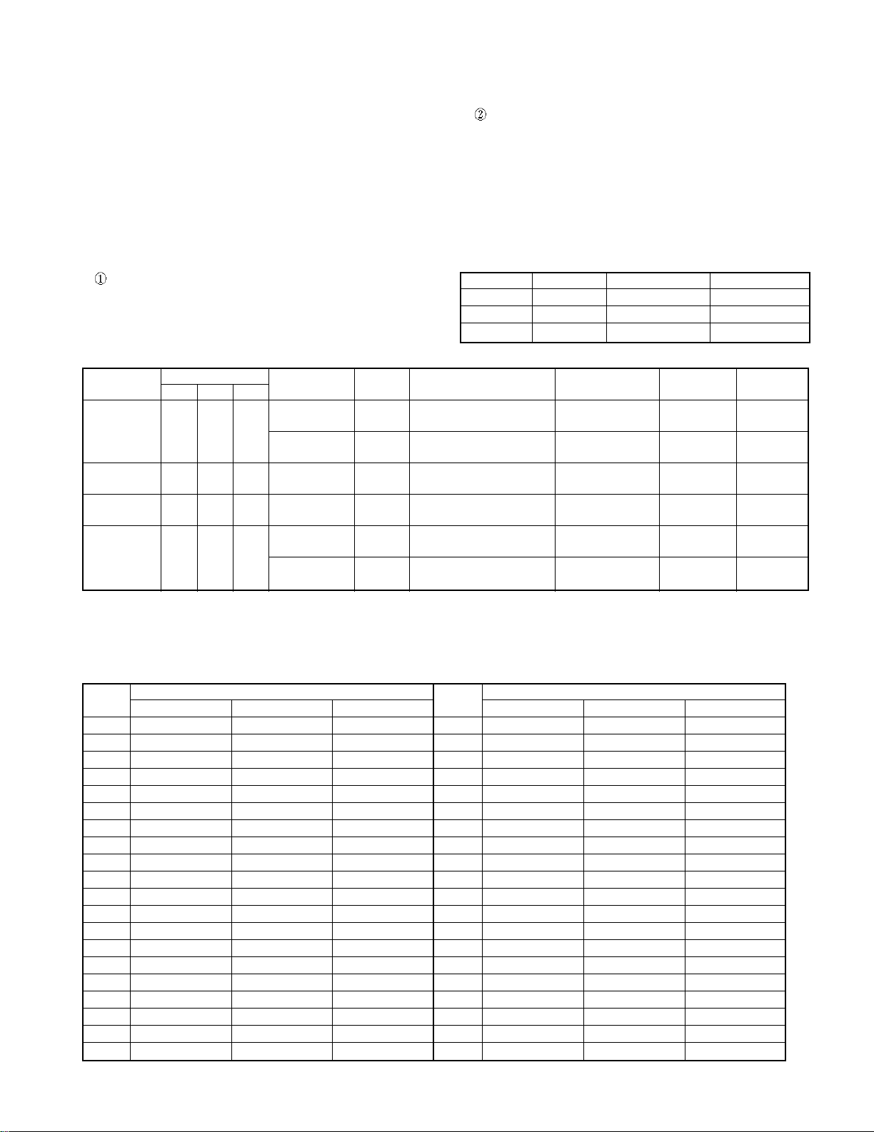
2-2Tuner Destination
Destination Destination SW u-COM
2 1 0 Destination Range
K2
M011
E1
X001E1
E/T (RDS) 1 0 1 E3
K2
V111
E1
BAND
FM 87.5MHz~108.0MHz 100kHz +10.7MHz 25kHz
AM 530kHz~1610kHz 10kHz +450kHz 10kHz
FM 87.5MHz~108.0MHz 50kHz +10.7MHz 25kHz
AM 531kHz~1602kHz 9kHz +450kHz 9kHz
FM 87.5MHz~108.0MHz 50kHz +10.7MHz 25kHz
AM 531kHz~1602kHz 9kHz +450kHz 9kHz
FM 87.5MHz~108.0MHz 50kHz +10.7MHz 25kHz
AM 531kHz~1602kHz 9kHz +450kHz 9kHz
FM 87.5MHz~108.0MHz 100kHz +10.7MHz 25kHz
AM 530kHz~1610kHz 10kHz +450kHz 10kHz
FM 87.5MHz~108.0MHz 50kHz +10.7MHz 25kHz
AM 531kHz~1602kHz 9kHz +450kHz 9kHz
MD Mechanism
• If a mechanism error occurred, the error indication is displayed as "MD ERR" on the display.
• The disc will be unloaded from MD mechanism automatically, if a disc is its in.
2. Discrimination of the Model and Destination
for Tuner
2-1 Discrimination of the Model
Models Destination Destination SW3 Destination SW4
RD-DV5MD M 0 0
RD-DV5 E/T 0 0
RD-DV7 T/E1/M1/X/V 1 1
Receiving Frequency
Channel Space IF RF
✽ Destination SW
SW0 : (78)Pin SW1 : (77)Pin SW2 : (76)Pin SW3 : (75)Pin SW4 : (74)Pin
( ) Pin No. of System Microcomputer : X29,IC15
3. Tuner Preset Frequency
P.CH
1 FM 87.50MHz FM 87.50MHz FM 87.50MHz 21 AM 530kHz AM 530kHz AM 531kHz
2 FM 108.0MHz FM 108.0MHz FM 108.0MHz 22 FM 87.50MHz FM 87.50MHz FM 87.50MHz
3 FM 98.00MHz FM 98.00MHz FM 98.00MHz 23 FM 87.50MHz FM 87.50MHz FM 87.50MHz
4 FM 108.0MHz FM 108.0MHz FM 89.10MHz 24 FM 87.50MHz FM 87.50MHz FM 87.50MHz
5 FM 90.00MHz FM 90.00MHz FM 90.00MHz 25 FM 87.50MHz FM 87.50MHz FM 87.50MHz
6 FM 87.50MHz FM 87.50MHz FM 87.50MHz 26 FM 87.50MHz FM 87.50MHz FM 87.50MHz
7 FM 87.50MHz FM 87.50MHz FM 87.50MHz 27 FM 87.50MHz FM 87.50MHz FM 87.50MHz
8 AM 530kHz AM 530kHz AM 531kHz 28 FM 87.50MHz FM 87.50MHz FM 87.50MHz
9 AM 1700kHz AM 1610kHz AM 1602kHz 29 FM 87.50MHz FM 87.50MHz FM 87.50MHz
10 AM 1000kHz AM 1000kHz AM 999kHz 30 FM 106.0MHz FM 106.0MHz FM 106.0MHz
11 AM 530kHz AM 630kHz AM 531kHz 31 FM 87.50MHz FM 87.50MHz FM 87.50MHz
12 AM 1440kHz AM 1440kHz AM 1440kHz 32 FM 87.50MHz FM 87.50MHz FM 87.50MHz
13 FM 106.0MHz FM 106.0MHz FM 106.0MHz 33 FM 87.50MHz FM 87.50MHz FM 87.50MHz
14 AM 530kHz AM 530kHz AM 531kHz 34 FM 87.50MHz FM 87.50MHz FM 87.50MHz
15 FM 87.50MHz FM 87.50MHz FM 87.50MHz 35 FM 87.50MHz FM 87.50MHz FM 87.50MHz
16 FM 98.00MHz FM 98.00MHz FM 98.00MHz 36 FM 87.50MHz FM 87.50MHz FM 87.50MHz
17 FM 98.50MHz FM 98.50MHz FM 98.50MHz 37 FM 87.50MHz FM 87.50MHz FM 87.50MHz
18 FM 87.50MHz FM 87.50MHz FM 87.50MHz 38 FM 87.50MHz FM 87.50MHz FM 87.50MHz
19 AM 990kHz AM 990kHz AM 990kHz 39 FM 108.0MHz FM 108.0MHz FM 108.0MHz
20 FM 97.40MHz FM 97.40MHz FM 97.70MHz 40 AM 1000kHz AM 1000kHz AM 945kHz
K1 K2 E1/E3
Frequency Frequency
P.CH
K1 K2 E1/E3
7
RD-DV5-S/DV7-L/DV5MD-S
CIRCUIT DESCRIPTION
4. Test Mode
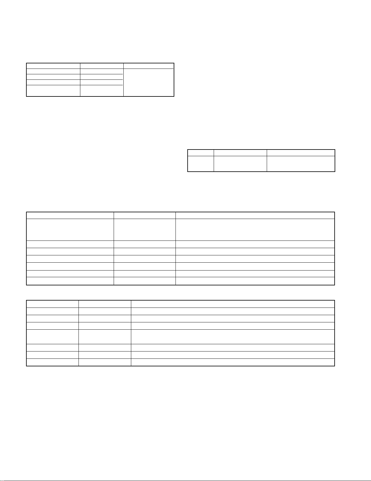
4-1 Setting method of the Test Mode
TEST MODE KEY SETTING
DVD TEST MODE DVD PLAY/PAUSE
MD TEST MODE MD PLAY/PAUSE Insert the AC cord to
MD MECHA. ADJ. MODE MD REC AC wall outlet with
FCT & SUB CLOCK SET/DEMO pressing the left key.
OSC DIAGNOSIS
4-2 Cancel of the test mode
• By turning the AC off, the system is initialized and the
test mode is canceled.
• Cancel the test mode only if the power switch is turned
off.
4-3 Contents of the Test Mode
• The muting during mode selection is not controlled in
the test mode.
• During the test mode, it can be operated in a special
manner that is different from an ordinary operation by
using the keys on the main body, specifically as shown
in the following tables.
4-4 FCT(Factory) and Sub clock OSC Diagnosis
Mode
4-4-1 Sub clock OSC Diagnosis Mode
The oscillation diagnosis (existence of oscillation and
measurement of period) of a sub clock is performed
before the test mode is entered. If the diagnosis result
is OK, the system enters the test mode.
If the diagnosis result is NG, the oscillation of the sub
clock is diagnosed again. If the result is OK, the system
enters the test mode. If the diagnosis result is continuously NG 5 times, the system stops with "ERR1"and
"ERR2"displayed.
4-4-2 Operation in the Test Mode
KEY LCD OPERATION
REPEAT OK or
✽✽✽✽ ERROR
Ex : ADSC ERROR
(Advanced Digital Servo Controller) ••• X35, IC1
✽✽✽✽ ERROR
Self diagnosis mode
(Refer to servo error code)
4-5 DVD Test Mode
KEYS DISPLAY OPERATION
DVD PLAY/PAUSE
(Cyclically changed the mode play Usual Indication Disc playback
and pause by pressing the key.)
STOP(in playback mode) DVD TEST Stop the playback and return to first step of this test mode
STOP(in stop mode) Region code Indicated the region code
SKIP UP/SKIP DOWN Usual Indication Skip up/down operation in the DVD playback.
SOUND J ITT ✽✽✽ % Shows jitter value (binary values vs time deviation of PLL clock).
MD REC Usual Indication FF Operation (triple speed)
REC MODE Usual Indication FB Operation (triple speed)
4-6 MD Test Mode
KEYS DISPLAY OPERATION
MD PLAY/PAUSE Usual Indication MD playback/pause
STOP MD TEST Stop the MD operation.
SKIP UP/DOWN Usual Indication MD track up/down
REC MODE Usual Indication Hi-speed O.T.E.(DVD î MD) operation in the stop mode.
Start the MD recording with LP4 mode.
MD REC Usual Indication Start analog recording (DVD î MD).
MODE Usual Indication Start digital recording (D. AUX î MD).
SET ALL ERASE Stop the MD operation , and start operation of ALL- ERASE if disc is recordable.
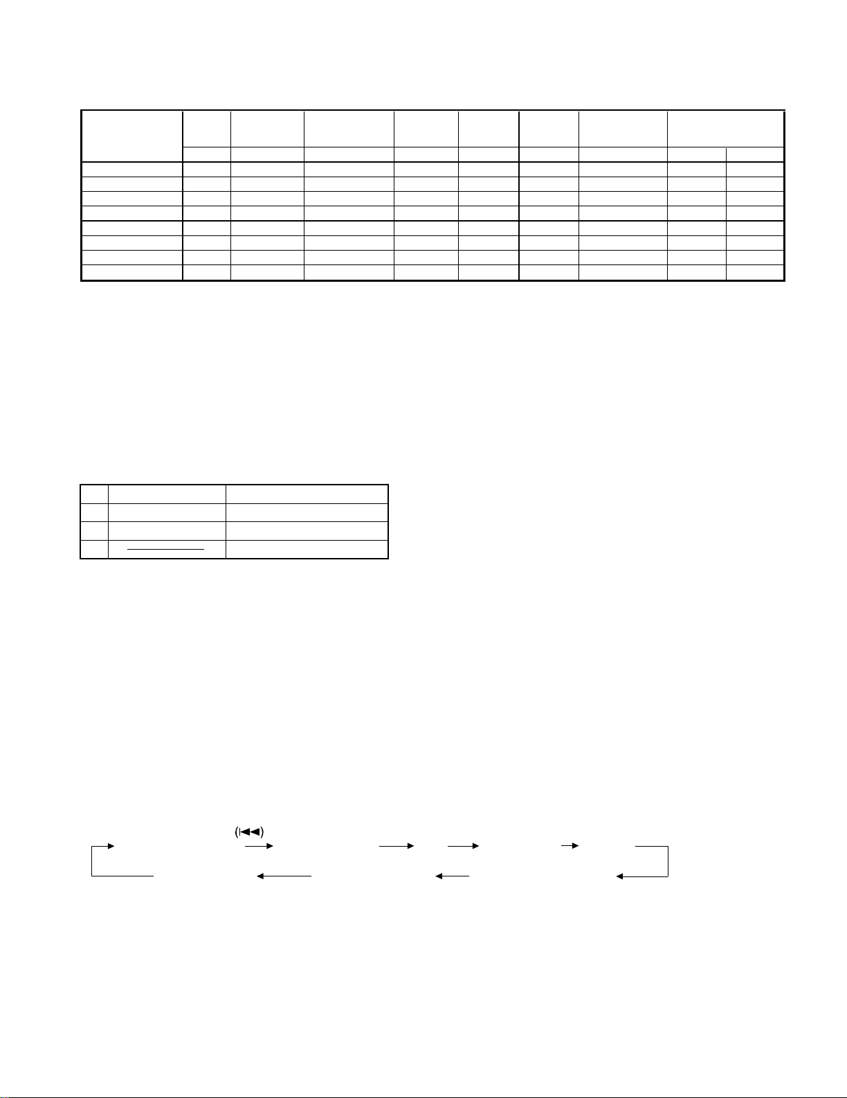
4-7 MD Mecha. Adjustment
1. Preparation for Adjustment You have to carry out the following test mode items if replace MD mechanism, pickup, head and pc board.
1-1 Procedure
1. Short-circuit #4(vss) and #7(wp) of IC1402(EEPROM).
2. Set the unit to test mode and carry out the every adjustment in test mode.
3. Stop the test mode by pressing the STOP key for 3 secs
4. Remove the short circuit of IC1402. Carry out reset start.
8
RD-DV5-S/DV7-L/DV5MD-S
TEMP EEPROM
✽ EEPROM
AUTO
AUTO
AUTO
✽ EEPROM ✽ ✽ Operation
Standard Set
data write
Pre
adjustment
AFB
data write check
Repair (replace)
Set value check adjustment adjustment
TEMP EEPROM SET Cancel Test Mode AUTO YOBI AUTO ADJ AUTO AFB Cancel Test Mode TEST PLAY TEST REC
Pickup - 12345678
Recording head - - - - - - - - 1
Mechanism - 12345678
PCB parts 12 3 4 56 7 89
MD microprocessor - 12--- - 34
MD LSI - - - 123 4 56
RF IC 12 3 4 56 7 89
EEPROM 12 3 4 56 7 89
1-2 Test disc
Type Test disc
1 High reflection disc TGYS1 (SONY)
2 Low reflection disc Recording minidisc
3 Head Adjusting transparent
Entering the specific mode
Whenever the button SKIP DOWN
is pressed, the mode is changed.
AUTO
(AUT YOBI) (AUTO AJST) (AUT AFB) (RST YOBI) (RESULT)
(MNU YOBI)(EEPROM SET) (MNU AJST)
pre-adjustment AUTO adjustment RESULT SUB RESULT
EEPROM setting MANUAL adjustment MANUAL pre-adjustment
AUT
CIRCUIT DESCRIPTION
note: figures order of steps." –" no need.
* Result of EEPROM
OK_EEPROM Write the data of setting values and AUTO-pre adjustment perfectly.
WR_EEPROM Write the data of setting values perfectly however not write AUTO pre-adjustment.
Carry out AUTO pre-adjustment and write data to EEPROM.
NG_EEPROM Not write the data of setting values.
Check the connection of MD microprocessor and EEPROM.
** Carry out the TEST-PLAY , TEST-REC and C1 error in test mode after AUTO_ADJ and AUTO_AFB.
2. Test Mode
1. Holding down the MD rec button and turn the power on. (State A)
2. To enter the test mode stop state(State B), press the STOP button.
3. Load the playback disc 1(high reflection disc) or recording disc 2(low reflection disc).
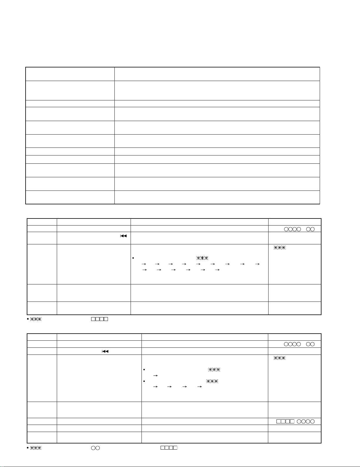
A MECHA TEST
B tsm
C LOADING
D AUTO AJST
ó (Press STOP key)
‡‡‡‡e‡‡
ó (MD DISC LOAD IN)
ó
---- TEST MODE STOP STATE
(When the STOP button is pressed in the D state, the indication B state is
restored.
To restore D state again, press the SKIP DOWN key once.
represents version of MD microcomputer
‡‡
9
RD-DV5-S/DV7-L/DV5MD-S
• Canceling the test mode
When the POWER button is pressed, the test mode is canceled, and the POWER OFF state is set.
• Test Mode
1. AUTO pre-adjustment mode • Automatic pre-adjustment is performed. (After adjustment the grating adjustment mode is set.)
• The adjustment value is output with the aid of system controller interface.
2. AUTO adjustment mode • Automatic adjustment is performed.
• The adjustment value is output with the aid of system controller interface.
• Continuous playback is performed. (Error rate indication, jump test)
4. RESULT sub-mode • The measurement value, set value and calculated value are indicated.
• The set value is changed manually (in servo OFF state).
3. AFB adjustment • Focus Balance adjustment is performed auto matically.
5. RESULT mode (final adjustment) • The set value (after calculation) is indicated.
• The set value is changed manually (in servo OFF state).
6. MANUAL pre-adjustment mode • RF side manual adjustment is performed.
• Focus and tracking signal offset setting is performed.
7. MANUAL adjustment mode • Focus and tracking signal ATT manual adjustment is performed.
8. EEPROM setting mode • EEPROM setting
9. TEST-PLAY mode • Continuous playback from the specified address is performed.
• C1 error rate measurement.
10. TEST-REC mode • Continuous recording from the specified address is performed.
• Change of record laser output (servo gain is also changed according to laser output)
11. EJECT mode • TEMP
• Laser power adjustment
setting (of EEPROM setting)
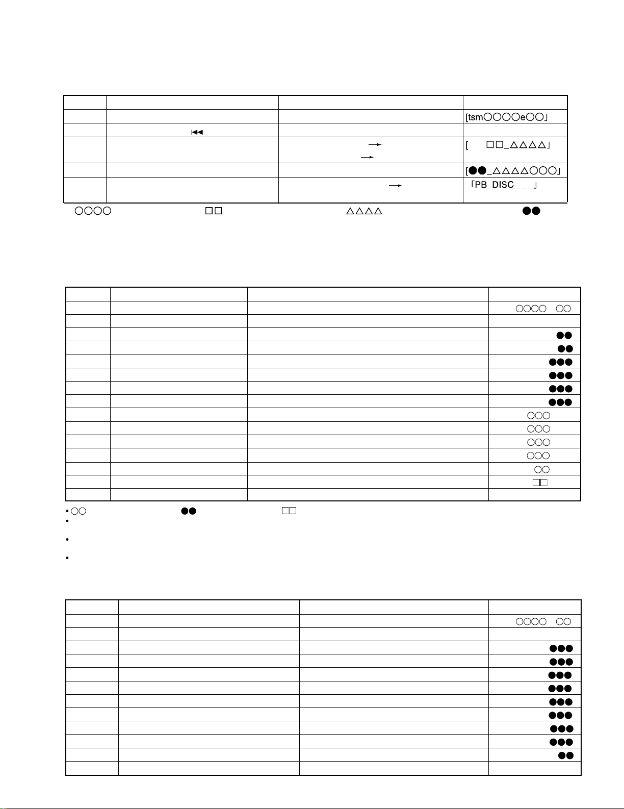
1. AUTO pre-adjustment mode (Low reflection disc only)
Step No.
Setting Method
Remarks Display
Step 1 Test mode STOP state [ t s m e ]
Step 2 Press once the SKIP DOWN( )
button eight times.
AUTO pre-adjustment menu [ AUT_ YOBI_ _ _ ]
Step 3 Press once the MD PLAY button. The slide moves to the innermost periphery, and automatic [ : _ _ _ _ _ _ _ ]
pre-adjustment is started.
During automatic adjustment changes as follows.
HAo
RFg SAg SBg PTG PCH GTG GCH RCG
SEG RFG SAG HAO HEO TCO LAO
End of adjustment If adjustment is OK, Step 4.
If adjustment is NG, Step 5.
Step 4 Grating adjustment, [ _ C O M P L E T E _ ]
adjustment value output
Press once the MD STOP button. STEP 2
Step 5 Adjustment value output [ AUT YOBI ]
Press once the MD STOP button. STEP 2 AUTO pre-adjustment menu
: Adjustment name, : Address
2. AUTO adjustment mode
Step No.
Setting Method
Remarks Display
Step 1 Test mode STOP state [ t s m e ]
Step 2
Press the SKIP DOWN( ) button one times.
AUTO adjustment menu [ A U T O _ A J S T _ ]
Step 3 Press once the MD PLAY button. The slide moves to the innermost periphery, and automatic [ : _ _ _ _ _ _ ]
adjustment is started.
In case of high reflection disc changes as follows.
PEG
HAG
In case of low reflection disc changes as follows.
PEG LAG GCG GEG LAG
End of adjustment If adjustment is OK, Step 4.
If adjustment is NG, Step 7.
Step 4 Adjustment value output
[ C O M P L E T E ]
Press the MD PLAY button. STEP 5
Press the MD STOP button. STEP 2
Step 5
Continuous playback (groove section)
[ a c ]
Step 6
Press the MD STOP button. STEP 2 AUTO adjustment menu
Step 7 Adjustment value output [ C a n ' t _ A D J . ]
Press the MD STOP button. STEP 2 AUTO adjustment menu
: Adjustment name, : Measurement value, : Address
CIRCUIT DESCRIPTION
10
RD-DV5-S/DV7-L/DV5MD-S
3. AUTO FAB adjusting mode
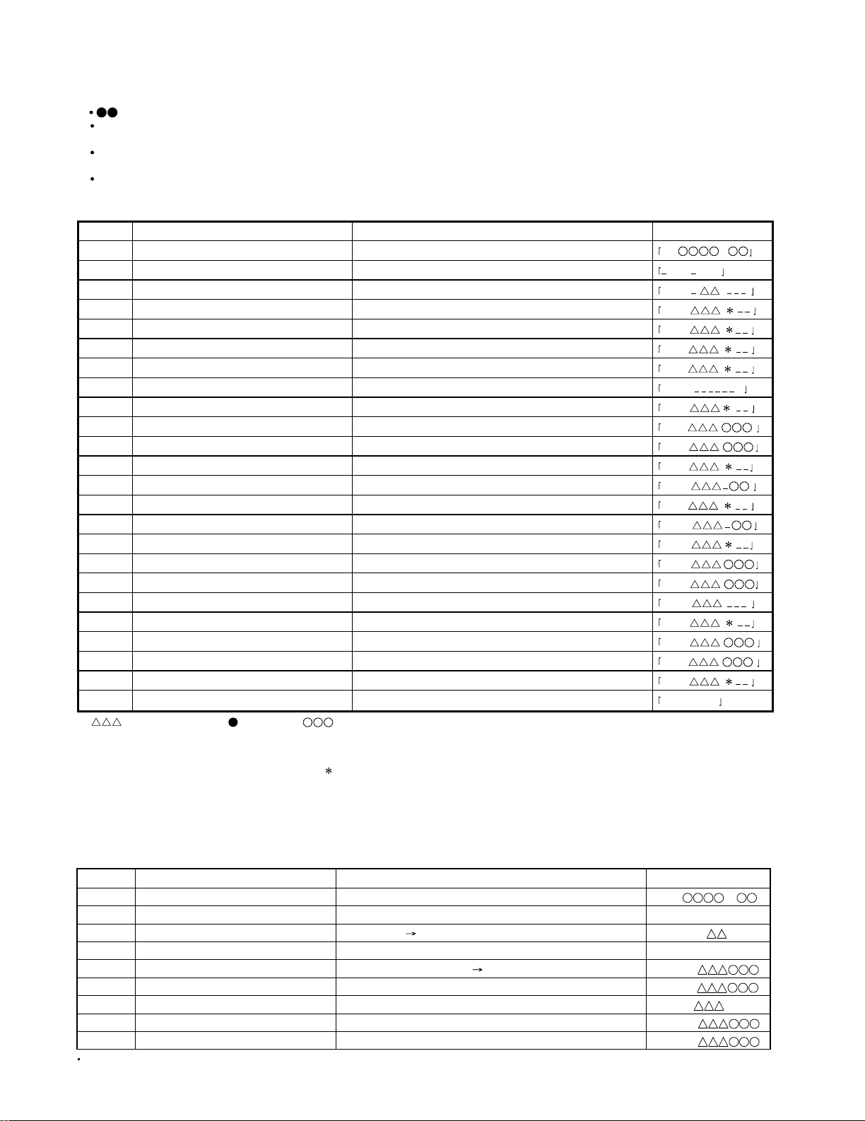
Step No. Setting Method Remarks Display
Step 1 Test mode STOP state
Step 2
Press the SKIP DOWN( ) button two times
AUTO FAB adjustment menu [_AUT_AFB_ _]
Step 3 Press the MD PLAY button 1 time
Step 4 Press the MD STOP button AUTO AFB adjustment menu, step 2
Step 5
• : measurement value : AFB value in measurement, : C1 error value in measurement, : AFB
value
• If the STOP button is pressed twice while the AUTO AFB adjustment is displayed, the state is change to the TEST mode
STOP state.
AFB
Step 1 Test mode STOP state [ t s m e ]
Step 2
Press the SKIP DOWN(4) button three times.
RESULT sub-menu [ _ R S T _ Y O B I _ ]
Step 3 Press once the MD PLAY button. Indication of measurement value [ P C H : _ _ _ _ ]
Step 4
Press once the SKIP DOWN(4) button.
Indication of measurement value [ G C H : _ _ _ _ ]
Step 5
Press once the SKIP DOWN(4) button.
Indication of measurement value [ S A G : _ _ _ ]
Step 6
Press once the SKIP DOWN(4) button.
Indication of measurement value [ S B G : _ _ _ ]
Step 7
Press once the SKIP DOWN(4) button.
Indication of measurement value [ S E G : _ _ _ ]
Step 8
Press once the SKIP DOWN(4) button.
Indication of measurement value [ S F G : _ _ _ ]
Step 9
Press once the SKIP DOWN(4) button.
Indication of measurement value [ H A O : _ _ _]
Step 10
Press once the SKIP DOWN(4) button.
Indication of measurement value [ H B O : _ _ _]
Step 11
Press once the SKIP DOWN(4) button.
Indication of measurement value [ H E O : _ _ _]
Step 12
Press once the SKIP DOWN(4) button.
Indication of measurement value [ H F O : _ _ _]
Step 13
Press once the SKIP DOWN(4) button.
Indication of measurement value [ T C O : _ _ _ _]
Step 14
Press once the SKIP DOWN(4) button.
Indication of pre-adjustment not completed (00)/completed (4B) [ A D J : _ _ _ _]
Step 15 Press once the MD STOP button. RESULT sub-menu state [ _ R S T _ Y O B I _ ]
4. RESULT sub-mode
Step No.
Setting Method
Remarks Display
: Measurement value, : Adjustment value, : Other various informations
When the (¡)button in remote controller is pressed while the setting is displayed, the setting increases,
and a new setting is stored in RAM.
When the (1)button in remote controller is pressed while the setting is displayed, the setting increases,
and a new setting is stored in RAM.
When the (¡) or (1)button in remote controller is pressed continously, steps is change by 100ms period.
Step 1 Test mode STOP state [ t s m e ]
Step 2 Press the SKIP DOWN(4) button four times. RESULT menu [ _ R S T U L T _ _ _ ]
Step 3 Press once the MD PLAY button. Indication of set value [ H A G : _ _ _ ]
Step 4
Press once the SKIP DOWN(4) button.
Indication of set value [ H B G : _ _ _ ]
Step 5
Press once the SKIP DOWN(4) button.
Indication of set value [ L A G : _ _ _ ]
Step 6
Press once the SKIP DOWN(4) button.
Indication of set value [ L B G : _ _ _ ]
Step 7
Press once the SKIP DOWN(4) button.
Indication of set value [ P E G : _ _ _ ]
Step 8
Press once the SKIP DOWN(4) button.
Indication of set value [ P F G : _ _ _ ]
Step 9
Press once the SKIP DOWN(4) button.
Indication of set value [ G E G : _ _ _ ]
Step 10
Press once the SKIP DOWN(4) button.
Indication of set value [ G F G : _ _ _ ]
Step 11
Press once the SKIP DOWN(4) button.
Indication of set value [ G C G : _ _ _ _ ]
Step 12 Press once the MD STOP button. RESULT menu state [ _ R E S U L T _ _ _ ]
5. RESULT mode (final adjustment)
Step No.
Setting Method
Remarks Display
CIRCUIT DESCRIPTION
End of automatic adj. step 4
High reflection disc step 5
Message output for 1 sec. AUTO AFB.
Adjustment menu(high reflection disc)
11
RD-DV5-S/DV7-L/DV5MD-S
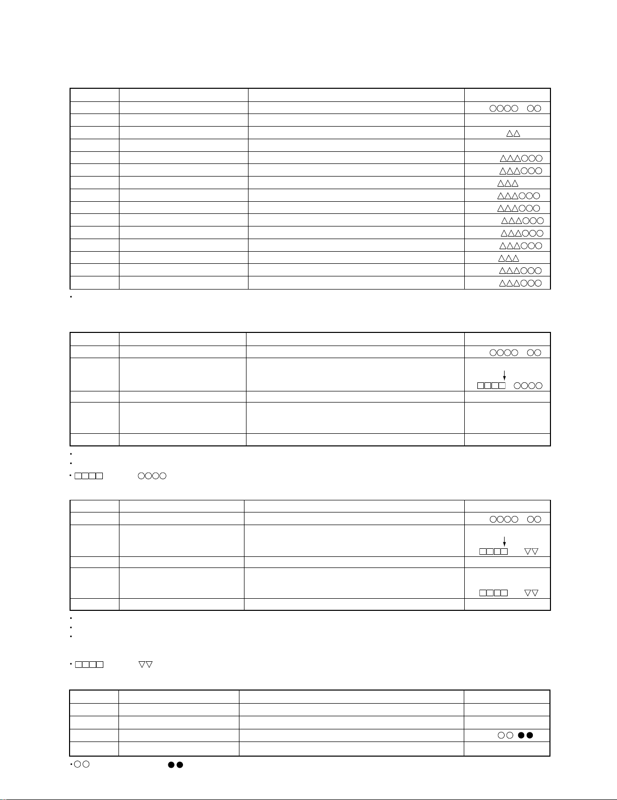
When the (¡)button in remote controller is pressed while the setting is displayed, the setting increases,
and a new setting is stored in RAM.
When the (1)button in remote controller is pressed while the setting is displayed, the setting increases,
and a new setting is stored in RAM.
When the (¡) or (1)button in remote controller is pressed continously, steps is change by 100ms period.
: Measurement value
6. MANUAL auxiliary adjustment mode (only low reflection disc)
Step No. Setting Method Remarks Display
Step 1 Test mode STOP state tsm e
Step 2 Press SKIP DOWN (4) button five times. MANUAL auxiliary adjustment mode
Step 3 Press once the MD PLAY button. Initial setting î Temperature measuring mode TMP :
Step 4 Press SKIP DOWN (4) button. Offset "0" setting î A signal offset tentative measurement HAo :
Step 5 Press SKIP DOWN (4) button. B signal offset tentative measurement HBo :
Step 6 Press SKIP DOWN (4) button. E signal offset tentative measurement HEo :
Step 7 Press SKIP DOWN (4) button. F signal offset tentative measurement HFo :
Step 8 Press SKIP DOWN (4) button. Laser ON LON :
Step 9 Press SKIP DOWN (4) button. ABMAXO measurement ABM :
Step 10 Press SKIP DOWN (4) button. Focus ATT (A signal) tentative setting SAg :
Step 11 Press SKIP DOWN (4) button. Focus ATT (B signal) tentative setting SBg :
Step 12 Press SKIP DOWN (4) button. Pit section LPFEFO measurement PEF :
Step 13 Press SKIP DOWN (4) button. Pit section COUT measurement
Step 14 Press SKIP DOWN (4) button. Groove section LPFEFO measurement
Step 15 Press SKIP DOWN (4) button. Groove section COUT level measurement
Step 16 Press SKIP DOWN (4) button. TCRMIO measurement TCR :
Step 17 Press SKIP DOWN (4) button. Tracking ATT (E signal) setting SEG :
Step 18 Press SKIP DOWN (4) button. Tracking ATT (F signal) setting
Step 19 Press SKIP DOWN (4) button. Indication of tracking EFMIO measurement g MI :
Step 20 Press SKIP DOWN (4) button. LPFABO measurement ABL :
Step 21 Press SKIP DOWN (4) button. Focus ATT (A signal) setting SAG :
Step 22 Press SKIP DOWN (4) button. Focus ATT (B signal) setting SAB :
Step 23 Press SKIP DOWN (4) button.
TCO :
Step 24 Press once the MD STOP button. MNU YOBI state
–
MNU–YOBI
-
• : Measurement value, : Set value : Account value
• When the (⁄) or (!) button in remote controller is pressed while the setting is displayed, the setting increases or decreases,
and a new setting is stored in ROM.
• When the (⁄) or (!) button in remote controller is pressed continuously, steps is change by 100ms period.
If the measurement value is within the OK range, " " appears on the 8th character.
OK range HAO, HB0, HEO, HFO : 0 0 0 h±2 0 0 h
ABM : 1E2h ∼ 9C7h PEF : 20Dh ∼ 785h
GEF : 20Dh ∼ 785h TCR : 030h ∼ 239h
ABL : 1E2h ∼ 9C7h TCO : 00h±20h
Step 1
Test mode STOP state
[ t s m e ]
Step 2
Press the SKIP DOWN(4) button six times.
MANUAL adjustment menu [ _ M N U _ A J S T _ ]
Step 3
Press once the MD PLAY button.
Initial setting Temperature measuring mode [ T M P : _ _ _ _ ]
Step 4
Press once the SKIP DOWN(4) button.
Laser ON [ L O N : _ _ _ _ _ _ ]
Step 5
Press once the SKIP DOWN(4) button.
Innermost periphery move Tracking ATT (E signal) setting [ P E G : ]
Step 6
Press once the SKIP DOWN(4) button.
Tracking ATT (F signal) setting [ P F G : ]
Step 7
Press once the SKIP DOWN(4) button.
Indication of tracking EFMIO measurement [ P M I : _ _ _ ]
Step 8
Press once the SKIP DOWN(4) button.
Focus ATT (A signal) setting [ H A G : ]
Step 9
Press once the SKIP DOWN(4) button.
Focus ATT (B signal) setting [ H B G : ]
7. MANUAL adjustment mode High reflection disc
Step No.
Setting Method
Remarks Display
If the MD STOP button is pressed twice while the MANUAL adjustment menu is displayed, the state is changed to the TEST
mode STOP state.
CIRCUIT DESCRIPTION
12
TCRS signal offset measurement
MNU YOBI
PCH :
GEF :
GCH :
SFG :
-
RD-DV5-S/DV7-L/DV5MD-S
8. TEST-PLAY mode
Step 1 Test mode STOP state [ t s m e ]
Step 2
Press once the SKIP UP(¢)button.
Press MD PLAY button.
Press MD PLAY button.
[ T E S T _ P L A Y _ ]
Step 4
Press
Step 3
Press the STOP button.
once the MD PLAY button.
During search the search output is set to "H", and it is
returned to "L" when continuous playback is started.
Continuous playback (groove section)
(Address + C1 error indication)
[a
c ]
Step 5
Press once the MD STOP button. TEST-PLAY menu [ T E S T _ P L A Y _ ]
[ T E S T _ P L A Y _ ]
Step No.
Setting Method
Remarks Display
If the MD STOP button is pressed while the TEST-PLAY menu is displayed, TEST mode STOP state is set.
If the MD PLAY button is pressed while the TEST-PLAY menu is displayed, continuous playback is started from the current pickup position.
: Adress, : Error late
Step 1 Test mode STOP state [ t s m e ]
Step 2
Press the SKIP DOWN(4) button six times.
MANUAL adjustment menu [ _ M N U _ A J S T _ ]
Step 3 Press once the MD PLAY button. Initial setting → Temperature measuring mode [ T M P : _ _ _ _ ]
Step 4
Press once the SKIP DOWN(4) button.
Laser ON [ L O N : _ _ _ _ _ _ ]
Step 5
Press once the SKIP DOWN(4) button.
Innermost periphery move → Tracking ATT (E signal) setting [ P E G : ]
Step 6
Press once the SKIP DOWN(4) button.
Tracking ATT (F signal) setting [ P F G : ]
Step 7
Press once the SKIP DOWN(4) button.
Indication of tracking EFMIO measurement (pit section) [ P M I : _ _ _ ]
Step 8
Press once the SKIP DOWN(4) button.
Focus ATT (A signal) setting [ L A g : ]
Step 9
Press once the SKIP DOWN(4) button.
Focus ATT (B signal) setting [ L B g : ]
Step 10
Press once the SKIP DOWN(4) button.
Outside periphery move → Track closs setting [ G C G : ]
Step 11
Press once the SKIP DOWN(4) button.
Tracking ATT (E signal) setting [ G E G : ]
Step 12
Press once the SKIP DOWN(4) button.
Tracking ATT (F signal) setting [ G F G : ]
Step 13
Press once the SKIP DOWN(4) button.
Indication of tracking EFMIO measurement (groove section) [ G M I : _ _ _ ]
Step 14
Press once the SKIP DOWN(4) button.
Focus ATT (A signal) setting [ L A G : ]
Step 15
Press once the SKIP DOWN(4) button.
Focus ATT (B signal) setting [ L B G : ]
Low reflection disc
Step No.
Setting Method
Remarks Display
If the MD STOP button is pressed twice while the MANUAL adjustment menu is displayed, the state is changed to the TEST mode
STOP state.
SKIP UP(¢)button twice.
9. TEST-REC mode
Step 1 Test mode STOP state [ t s m e ]
Step 2
Press the
[ T E S T _ R E C _ _ ]
Step 3 Press the STOP button.
Step 4 Press
Continuous playback
(groove section)
once the MD PLAY button. During search the search output is set to "H", and it is
returned on "L" when continuous playback is started. (Address
+
C1 error indication) [ a
p w ]
[ a
p w ]
Step 5 Press once the MD STOP button. TEST-REC menu [ T E S T _ R E C _ _ ]
[ T E S T _ R E C _ _ ]
Step No.
Setting Method
Remarks Display
If the MD STOP button is pressed while the TEST-PLAY menu is displayed, TEST mode STOP state is set.
If the MD PLAY button is pressed while the TEST-REC menu is displayed, continuous record is started from the current pickup position.
If
: Measurement value, : Setting value.
the (¡) or (1) button in remote controller is pressed in TEST-REC mode and continuous record mode,
the laser record power changes.
(Servo gain changes also according to the record power.)
: Adress, : Laser power cord
10. EJECT mode
Step 2
Step 1
Test mode
Test mode STOP state
EJECT Eject of MD discstate [ _ _ E J E C T _ _ _ ]
Step 3 Press
SKIP UP(¢)
button. Temperature standard value setting. [ TEMP ]
Step 4 Press STOP button. [ _ _ EJECT _ _ _ _ ]
Step No.
Setting Method
Remarks Display
CIRCUIT DESCRIPTION
13
RD-DV5-S/DV7-L/DV5MD-S
CIRCUIT DESCRIPTION
5. Port Description of Microcomputer (X29, IC15)
Port No. Port Name I/O Function
1 FL DATA O Data output to FL driver.
2 FL CLK O Clock output to FL driver.
3 FAN CONT O Fan control port.
4 DVD MUTE4 O Mute control port for DVD.
5 ROM DATA - Unused.
6 ROM CLK - Unused.
7 NC - Unused.
8 BYTE - Connected to ground.
9 CNVSS - Connected to ground.
10 XCIN I Clock input (32.768kHz).
11 XCOUT O Clock output (32.768kHz).
12 RESET I Reset signal input.
13 XOUT O Main clock output (10MHz).
14 VSS - Connected to ground.
15 XIN I Main clock input (10MHz).
16 VCC - Supply voltage (+5V)
17 NMI - Connected to VCC.
18 u-COM CE I Detection port for power failure
19 REMOCON I Remote control signal input.
20 RDS CLK I RDS clock signal input. (E/T type only)
21 FL STB O Strobe signal output to FL driver.
22 DVD NRST I Reset signal input of DAC for DVD. (Unused)
23 DVD POWER O DVD power on port.
24 DVD A O On/off port of high voltage for DVD tray motor.
25 DVD TRAY/TRV O Control port that sense of rotation for DVD motor driver.
26 DVD B O On/off port of low voltage for DVD tray motor.
27 DVD OPEN SW I Input port of tray switch for DVD.
28 DVD CLK I Clock signal input for DVD communication.
29 DVD SIN I Data input for DVD communication.
30 DVD SO0 O Data output for DVD communication.
31~34 NC - Unused.
35 KDATA O Data output for MD communication.
36 MD DATA I Data input for MD communication.
37 MD DSCK O Clock output for MD communication.
38 MD DSTR O Strobe output for MD communication.
39 MD SEARCH O MD search output.
40 MD RST O Reset signal output to MD mecha. Microprocessor.
41 NC - Unused.
42 MD ST O Strobe signal output to MD mecha. Microprocessor.
43 NC - Unused.
44 HP IN I Detection port of headphones jack.
45 ENPH CONT - Unused.
46 NC - Unused.
47 RDS DT O RDS synchronized data output. (E/T type only)
48 CS-SP O
49 F-SP O Relay control port of front speaker.
50 AMUTE O Audio mute control port. Mute off Mute on
51 MD MUTE O MD search mute. MD search Others
52 AMP SW O Control port of A class amplifier.
53 POWER O Control port of power relay. Power on Power off
54 S VIDEO SW2 O Change-over the video switch 2.
Relay control port of center and sub woofer speakers. 4ch SP. 4ch SP.
(RD-DV7 only) On Off
Active
HL
Front SP. Front SP.
On Off
14

RD-DV5-S/DV7-L/DV5MD-S
CIRCUIT DESCRIPTION
Port No. Port Name I/O Function
55 S VIDEO SW1 O Change-over the video switch 1.
56 ST I Detection port of stereo signal for tuner. mono stereo
57 SD I Detection port of SD signal for tuner.
58 PLL DO I IF count input of PLL IC for tuner.
59 PLL CE O CE output of PLL IC for tuner.
60 PLL CLK O Clock output of PLL IC for tuner.
61 PLL DATA O Data output of PLL IC for tuner.
62 VCC - Supply voltage (+5V)
63 TU PROT(9V) - Protection signal input for tuner.
64 GND - Ground port.
65 V MUTE O Video mute control port.
66 TU DC OFF O Port of supply voltage for tuner.
67~69 SEL SW(0~2) O Control port of TC9215AF (X29, IC3). (RD-DV7 only)
70 DIG SEL1 O Digital selector 1 output.
71 CVOL CLK O Clock output to TDA7309 (X29, IC4). (RD-DV7 only)
72 CVOL DATA O Data output to TDA7309 (X29, IC4). (RD-DV7 only)
73 PROTECT I Protection signal input.
74 INI SW4 I Discrimination port of MD. without MD with MD
75 INI SW3 I Discrimination port of 4ch /2ch for amplifier. 4ch mode 2ch mode
76~78 INI SW2~INI SW0 I Discrimination port of tuner destination.
79 DIN ON/OFF SW O Control port of digital input on/off. analog input digital input
80 DOUT ON/OFF SW O Control port of digital output.
81 DIG SEL2 O Change-over the digital input selector for MD.
82 PVOL STB O Strobe signal output to M62492 (X29, IC1).
83 PVOL CLK O Clock output to M62492 (X29, IC1).
84 PVOL DATA O Data output to M62492 (X29, IC1).
85 STANDBY LED O Control port of standby led (red). power off power on
86 TIMER LED O Control port of timer led (green).
87 ENCODER CW I Encoder (Vol/Multi Cont.) signal input for CW.
88 ENCODER CCW I Encoder (Vol/Multi Cont.) signal input for CCW.
89 TH PROT2 I Detection port for temperature.
90 PROT(3.3V) I Detection port of protection for current.
91 TU SLEVEL I Signal level input for tuner.
92 TH PROT2 I Detection port of protection for temperature.
93 SP LEVEL I Signal level input for audio.
94,95 KEY0,KEY1 I A/D key signal input.
96 GND - Ground port.
97 DVD IN SW I Close switch input of tray for DVD mecha.
98 VREF - Port for the A/D, D/A reference voltage (+5.0V).
99 AVCC - Port for the A/D, D/A supply voltage (+5.0V).
100 FL RES O Reset signal output to FL driver.
No digital digital
Active
HL
output output
Timer
standby
Others
15
RD-DV5-S/DV7-L/DV5MD-S
CIRCUIT DESCRIPTION
6. Port Function of DVD Microcomputer : MN102L62GGB (X35, IC201)
Port No. Port Name I/O Function
1 WAIT I Bus wait port.
2 NRD(ODC/AVDEC/SRAM) O Bus read port.
3 NWEL O Unused.
4
(ODC/AVDEC/SRAM/ROM)
5 RAMCS(SRAM) O SRAM chip select.
6 ODCCS O ODC chip select.
7 AVCS(AVDEC) O AV decoder chip select.
8 ROMCS(ROM) O Flash ROM chip select.
9 SCLOCK(VDAC) O Clock output to VDAC (X35, IC600).
10 SDATA(VDAC) O Data output to VDAC (X35, IC600)
11 FRD(ROM) O Flash ROM read port.
12 WORD - Connected to VDD (+3.3V).
13~16 CPUADR0~3 O Bus address (0~3).
17 VDD - Supply voltage (+3.3V).
18 SYSCLK(AVDEC) O Clock output to AV decoder (X35, IC300).
19 VSS - Connected to GND.
20 XI I Connected to GND.
21 XO O Unused.
22 VDD - Supply voltage (+3.3V).
23 OSCI(CLK135) I System clock input (13.5MHz).
24 OSCO O Unused.
25 MODE I Processor mode selection.
26~33 CPUADR4~11 O Bus address (4~11).
34 AVDD - Supply voltage (+3.3V).
35~42 CPUADR12~19 O Bus address (12~19).
43 VSS - Connected to GND.
44 CPUADR20 O Bus address (20).
45 25BSY O Busy data output. Normal Busy
46 STBPSL O Unused.
47 HFMON O HF monitor output.
48 KMODE O Selection for writing the ROM. Writing Normal
49 AMUTE O Audio mute control.
50 CIRCEN(ENC) O Enable to Digital Servo Controller (X35, IC1).
51 PROGSW I Change-over the component terminal.
52 STBTI O Strobe output to MP3 decoder (X35, IC900).
53 FRSW O Flash ROM 1, 2 (X35, IC207, 215) change-over. Default
54 VDD - Supply voltage (+3.3V).
55 FEPEN O Enable to FEP (traverse).
56 CLKSEL O Clock selection.
57 STBDAC2 O Strobe output to ADAC (X25, IC205).
58 STBSP1 O Strobe output to serial-parallel converter (X25, IC224).
59 STBDAC1 O Strobe output to ADAC (X25, IC204).
60 ADSCEN(ENS) O Enable to Digital Servo Controller (X35, IC1).
61 VSS - Connected to GND.
62 WMINT I Interruption port from Water Mark Detector (X35, IC500).
63 E2CS O Chip select to EEPROM (X33, IC206).
64 SCSIBN O Enable control to jig for writing the ROM.
65 196BSY I Busy data input. Normal Busy
66 VDD - Supply voltage (+3.3V).
67 SCLK0 O
NWEH
16
O Bus read port.
SIO0 clock output to communicate between main
microcomputer and DVD system microcomputer.
Active
HL
Expan
Mode
RD-DV5-S/DV7-L/DV5MD-S
CIRCUIT DESCRIPTION
Port No. Port Name I/O Function
68 SI0 I
69 SO0 O
70 SCLK1 O SIO1 clock output for control ICs.
71 SI1 I SIO1 data input for control ICs.
72 SO1 O SIO1 data output for control ICs.
73 PULL UP0 I Unused.
74 PULL UP1 I Unused.
75 NMI I Unused.
76 ADSCINT I Interruption port from Digital Servo Controller (X33, IC1).
77 ODCINT I Interruption port from Optical Disc Controller (X33, IC101).
78 AVINT I Interruption port from AV decoder (X33, IC301).
79 ICRST O Reset signal output to periphery ICs.
80 MP3INT I Interruption port from MP3 decoder (X33, IC900).
81 ADSEP I Unused.
82 RST I Reset signal input.
83 VDD - Supply voltage (+3.3V).
84~91 CPUDT0~7 I/O Bus data (0~7) input and output.
92 VSS - Connected to GND.
93~100 CPUDT8~15 I/O Bus data (8~15) input and output.
SIO0 data input to communicate between main
microcomputer and DVD system microcomputer.
SIO0 data output to communicate between main
microcomputer and DVD system microcomputer.
Active
HL
17
RD-DV5-S/DV7-L/DV5MD-S
CIRCUIT DESCRIPTION
7. Port Function of AV decoder : MN677533MP (X35, IC301)
Port No. Port Name I/O Function
1,9,32,46,53,73,104
116,142,156,160,166
172,179,184,191,197
205
2~4,6~8,10,201
203,204,206,207
5,14,27,42,52,60,70
83,92,105,120,147
157,163,169,176,182
186,194,200,208
12,37,66,79,96,112
145,174,188,202
23,24 HMD1,HMD0 - Connected to digital supply voltage (+3.3V).
33~36,38~41
43~45
47~51,54~59
61~65
74~78,80~82 STD0~STD7 I Bit stream parallel input 0~7.
18
11 CLK121 - Connected to digital ground.
13 XRST I System reset input. L : Reset
15 CLK81 - Connected to digital ground.
16 PLLAVDD - Main PLL supply voltage (+3.3v).
17 TCPOUT O Unused.
18 PLLAVSS - Connected to digital ground.
19 CLK27 I System clock input (27MHz).
20 PLLTEST I Test input port for main PLL. L : Fixed
21 CKIO I Decode clock change-over.
22 PLLVDD - Supply voltage (+2.5V) of internal logic for main PLL..
25 XHINT O Interruption to DVD microcomputer. L : Active
26 XDK O Acknowledgment to DVD microcomputer. L : Active
28 XWR I Write enable from DVD microcomputer.
29 XRD I Read enable from DVD microcomputer.
30 XCS I Chip select from DVD microcomputer.
31 HCLK I Clock input from DVD microcomputer.
67 AUDSTR I Valid signal of bit stream input data.
68 ARQ O Unused.
69 VSTR I Clock signal input for bit stream.
71 VRQ O Request of program stream.
72 AVRTM I Signal input of punctuation for sector.
84 EXTCK I fs= 192kHz: 192fs= 36.864MHz output
85 APLLVDD - Supply voltage (+2.5V) of internal logic for Audio PLL..
86 P5481 - Audio PLL ground.
87 PHCOPMO O Audio PLL phase comparison output.
88 APLLAVSS - Audio PLL ground.
89 NC - Unused.
90 APLLAVDD - Supply voltage (+3.3V) for Audio PLL..
91 ACKIO - Connected to digital ground.
92 VSS - Digital ground.
93 DCTEST - Connected to digital ground.
VDD - Digital supply voltage (+3.3V).
MA0~MA11 O SDRAM address 0~11
VSS - Digital ground.
LVDD - Digital supply voltage (+2.5V) for internal logic.
HA1~HA11 I Address input from DVD microcomputer.
HD0~HD15 I/O DVD microcomputer data bus 0~15.
Audio clock input.
fs= 48kHz: 768fs= 36.864MHz output
fs= 96kHz: 384fs= 36.864MHz output
fs= 44.1kHz: 768fs= 33.8688MHz output
fs= 88.2kHz: 384fs= 33.8688MHz output
fs= 176.4kHz: 192fs= 33.8688MHz output
RD-DV5-S/DV7-L/DV5MD-S
CIRCUIT DESCRIPTION
Port No. Port Name I/O Function
94,95 TESTSEL1,0 - Connected to digital ground.
97~102,106,108 TEST4~TEST9
109 TEST3,1,0
103 CLKMON O Unused.
107 RFF O Unused.
110 IECOUT O IEC958 format data output.
111 DMIX O Audio down mix signal output.
113 DACCK O fs= 192kHz: 192fs= 36.864MHz output
114 LRCK O LR clock output.
115 SRCK O Bit clock output.
117~119 ADOUT(0~2) O Audio data output (0~2).
121 XPOWD I DAC power down control input.
122 VREFC I DAC reference voltage input for C signal.
123 IREFC I DAC bias current setting port for C signal.
124 COMPC I Capacitance connection for DAC (C signal) stabilization.
125 VCOUT O Unused.
126,136 AVDD - Analog supply voltage (+3.3V) for DAC.
127 VREFCB I DAC reference voltage input for CB signal.
128 IREFCB I DAC bias current setting port for CB signal.
129 COMPCB I Capacitance connection for DAC (CB signal) stabilization.
130 VCBOUT O Unused.
131,141 AVSS - Analog ground for DAC.
132 VREFCR I DAC reference voltage input for CR signal.
133 IREFCR I DAC bias current setting port for CR signal.
134 COMPCR I Capacitance connection for DAC (CR signal) stabilization.
135 VCROUT O Unused.
137 VREFY I DAC reference voltage input for Y signal.
138 IREFY I DAC bias current setting port for Y signal.
139 COMPY I Capacitance connection for DAC (Y signal) stabilization.
140 VYOUT O Unused.
143 XYSYNCO I/O Vertical synchronizing signal input/output.
144 XHSYNCO I/O Horizontal synchronizing signal input/output.
146 VCLK O Clock output for digital video data output.
148~155 VD0~VD7 O Digital video data output (0~7).
158,159,161,162,164
165,167,168,170,171
173,175,177,178,180
181
183 MCKI I Clock input from SDRAM.
185 MCK O Clock output to SDRAM.
187 DQMLE O Lower bite data, mask signal of expander SDRAM.
189 DQMLM O Lower bite data, mask signal of main SDRAM.
190 DQMUE O Upper bite data, mask signal of expander SDRAM.
192 DQMUM O Upper bite data, mask signal of main SDRAM.
193 XWE O Write enable signal of SDRAM.
195 XCAS O CAS signal of SDRAM.
196 XRAS O RAS signal of SDRAM.
198 XCSE O Chip select signal of expander SDARM.
199 XCSM O Chip select signal of main SDARM.
✽ MN677521HB X35-229, IC300 DV-5900M/DVF-R9050
✽ MN677533MP X35-230, IC301 DV-5050M/DVF-J6050
MDQ0~MDQ15 I/O SDRAM data bus (0~15).
O Unused.
Over sampling DAC clock output.
fs= 48kHz: 384fs= 18.432MHz output
fs= 96kHz: 384fs= 36.864MHz output
fs= 44.1kHz: 384fs= 16.9344MHz output
fs= 88.2kHz: 384fs= 33.8688MHz output
fs= 176.4kHz: 192fs= 33.8688MHz output
RMD-SJ5, RD-DV5/7
19
 Loading...