

Kenwood RC-2000 Service manual
MOBILE CONTROLLER
RC-2000
SERVICE MANUAL
© 2001-2 PRINTED IN JAPAN
B51-8571-00 (N) 697
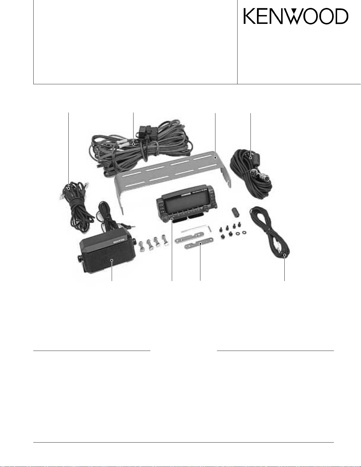
Modular cable
(E30-3409-05)
DC cord
(E30-3406-05)
Angle
(A13-0635-03)
Trunk cable
(E30-3407-05)
Speaker assy
(T19-0116-05)
Control panel
CONTENTS
CIRCUIT DESCRIPTION ............................ 2
SEMICONDUCTOR DATA ........................ 3
DESCRIPTION OF COMPONENTS .......... 4
TERMINAL FUNCTION ............................. 4
PARTS LIST ............................................... 5
EXPLODED VIEW...................................... 6
Spacer
(J30-0521-04) x 2
Trunk cable
(E30-3408-05)
PACKING ................................................... 7
PC BOARD VIEWS
DISPLAY UNIT (X54-3290-00) .............. 9
SCHEMATIC DIAGRAM .......................... 13
BLOCK DIAGRAM ................................... 15
SPECIFICATIONS ................. BACK COVER
RC-2000
9V
D30R42
D24D25R39
D26D27R40
D28D29R41
IC4
Microprocessor
DIM3 Q8
DIM2
Q7
DIM1
DIM0
Q6
Q5
Q3
R8
R10
R9
R12
R11
R14
R13
LCD ASSY
Q2
Q4
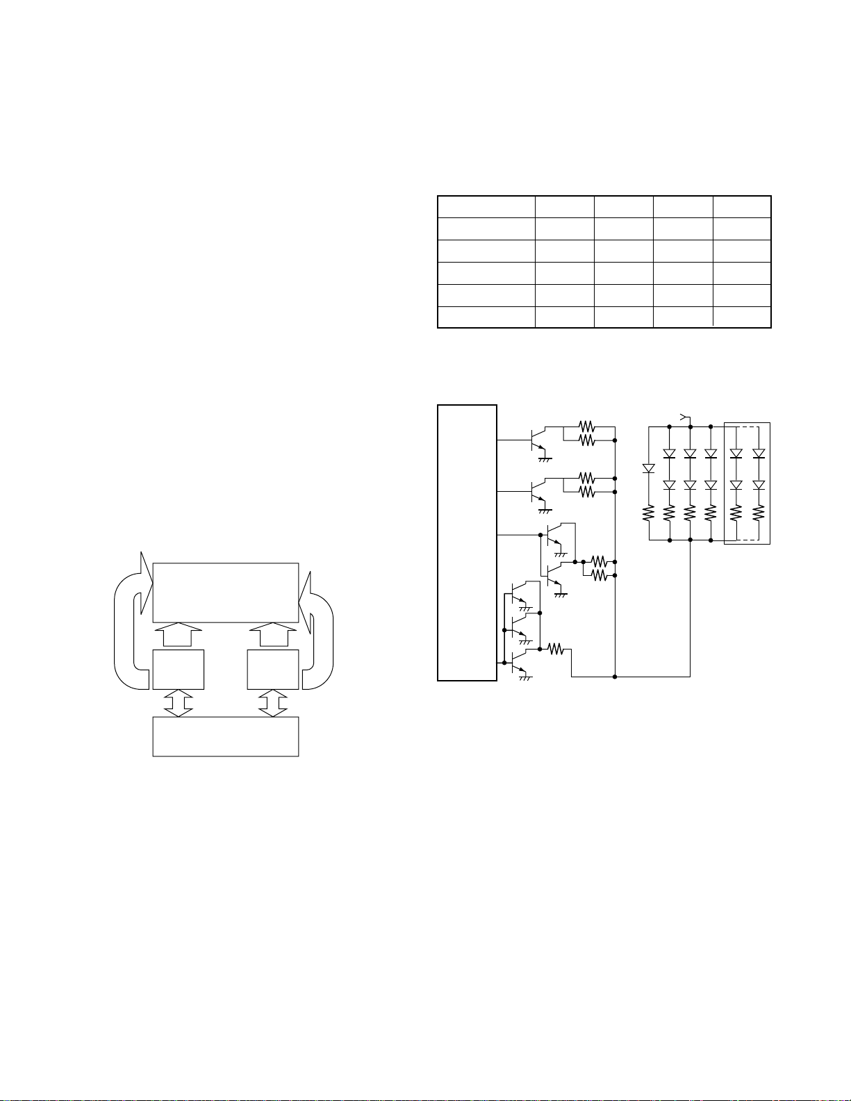
CIRCUIT DESCRIPTION
Panel Section (LCD ASSY : B38-0829-05)
The panel section controls serial communications with
the main unit control section, the key input circuit, the display circuit, and the dimmer circuit through the microprocessor (IC4).
■ Serial communications circuit
A buffer amp is inserted in order to protect the microprocessor ports.
■ Key, Volume input circuit
Circuits to operate the panel section keys are connected
to each microprocessor port. The PSW key is pulled up and
the other keys are pulled up with software within the microprocessor. Rotary encoder operating circuits are connected
directly to the microprocessor. The control divides the
power supply voltage, reads the A/D port of the microprocessor, and transfers that data to the main unit.
■ Display circuit
Display section is a 188 x 54-dot full-dot matrix LCD controlled by two LCD. As shown is Figure 1, the master IC
(IC2) side is connected to 22 common dots and 88 segment
dots and the slave IC (IC1) side is connected to 33 common
dots and 100 segment dots. The LCD drive voltage is obtained by raising the power supply voltage (5V) within the IC.
■ Dimmer circuit
The dimmer circuit switches the lamp brightness to one
of four levels or OFF (See table1). The current flowing to the
LEDs is varied by selecting resistors from R8 to R14.
Dimmer level DIM 0 DIM 1 DIM 2 DIM 3
1HLLL
2LHLL
3LLHL
4 LLLH
OFF L L L L
Table 1 Port logic
22
COM
88
SEG
LCD
Driver
IC2
Microprocessor
188 × 54 (dot)
Fig. 1 Display circuit
LCD
IC4
100
SEG
LCD
Driver
IC1
33
COM
X54-329
Fig. 2 Dimmer circuit
2
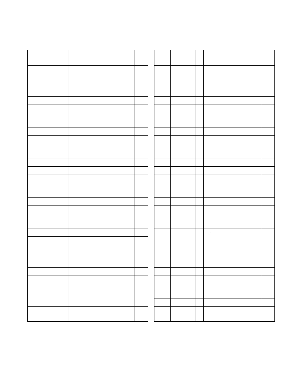
SEMICONDUCTOR DATA
CPU : 30622M8759GP (Display Unit IC4)
Pin No. Port name I/O Function Active
level
1 KYCALL I [AT] key input L
2 KYVFO I [Q. IN] key input L
3 KYMR I [EASY] key input L
4 KYPM I [PM] key input L
5 KYMNU I [RIT] key input L
6 BYTE I Select 8-bit data bus (5C)
7 CNVSS I
8 FUNC I [F1] key input L
9 KYF1 I [F2] key input L
10 RESET I Reset
11 XOUT O Clock output
12 VSS - GND
13 XIN I Clock input
14 VCC - Power input
15 NMI (I) Not used
16 INT2 I Interrupt from serial input port
17 INT1 I Encoder pulse 1 input
18 INT0 I Encoder pulse 2 input
19 KYF2 I [F3] key input L
20 KYF3 I [F4] key input L
21 NC I Not used (VCC)
22 NC I Not used (VCC)
23~26 DIM3~0 O Dimmer output
27 PSW O Power SW control output
28 BS O Beat shift output
29 NC I Not used (VCC)
30 NC I Not used (VCC)
31 KYF4 I [F5] key input L
32 KYF5 I [F6] key input L
33 TXD0 O Serial port for connecting to
34 RXD0 I Serial port for connecting to
Select memory expansion mode
TX-RX uint
TX-RX uint
RC-2000
Pin No. Port name I/O Function Active
level
35 NC I Not used (VCC)
36 NC I Not used (VCC)
37~41 NC I Not used
42 RD - Read signal
43 NC - Not used
44 WR - Write signal
45 LCDA0 O LCD address 0
46 LCDCD2 O LCD chip select 2
47 LCDCD1 O LCD chip select 1
48 CS0 - Flash ROM chip select signal
49 A19 - Not used (Open)
50~59 A18~9 - Address bus 18~9
60 VCC - Power input
61 A8 - Address bus 8
62 VSS - GND
63~70 A7~0 - Address bus 7~0
71~78 LCDD7~0 I/O LCD data bus 7~0
79~86 D7~0 - Data bus 7~0
87 LCDRD O LCD read terminal
88 LCDWR O LCD write terminal
89 LCDRES O LCD reset
90 POWER I [ ] key input L
(key interrupt)
91 B-AFVR I Sub band R AF VOL (A/D)
92 B-SQVR I Sub band R SQ VOL (A/D)
93 A-AFVR I Main band L AF VOL (A/D)
94 AVSS - Analog power input (GND)
95 A-SQVR I Main band L SQ VOL (A/D)
96 VREF - A/D reference voltage input
97 AVCC - Analog power input (5C)
98 MHz I [TUNING CONTROL] key input L
99 B_KEY I [SUB AF CONTROL] key input L
100 A_KEY I
[MAIN AF CONTROL] key input
L
3
RC-2000
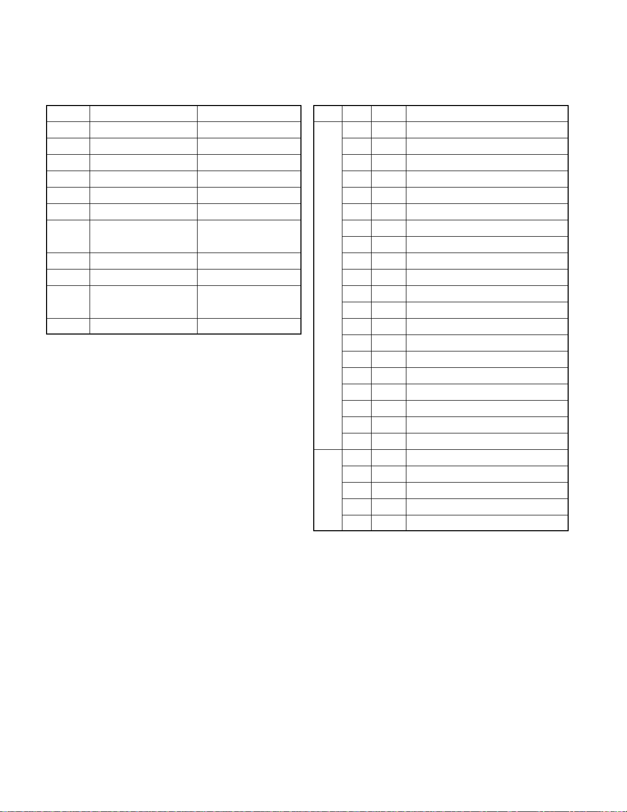
DESCRIPTION OF COMPONENTS / TERMINAL FUNCTION
Display Unit (X54-3290-00)
Ref. No. Application/Function
IC1 Serial transmission buffer
IC2 Serial transmission buffer
IC3 AVR with reset function
IC4 Control microcomputer
IC5 ROM
Q1 Power switch
Q2~4,6, Dimmer
7,9,10
D1 Reverse flow prevention
D2 Reset circuit
D3-23 Over-voltage prevention
(Surge elimination)
D24~30 Key illumination
Display Unit (X54-3290-00)
Operation/Condition/Compatibility
CN No. Pin No.
CN1 1 D7 LCD driver data
CN2 1 GND
CN3 2 VR power
Name Function
2 D6 LCD driver data
3 D5 LCD driver data
4 D4 LCD driver data
5 D3 LCD driver data
6 D2 LCD driver data
7 D1 LCD driver data
8 D0 LCD driver data
9 RD LCD driver RD
10 WR LCD driver WR
11 A0 LCD driver A0
12 GND GND
13 CS2 LCD driver chip select
14 CS1 LCD driver chip select
15 RES LCD driver reset
16 VDD LCD driver VDD
17 VL Illumination LED control
18 VL Illumination LED control
19 PB Illumination LED power
20 PB Illumination LED power
3 switch
4 VR voltage
5 SQL voltage
4
 Loading...