

REGULATED DC POWER SUPPLY
PW-A SERIES
SERVICE MANUAL
KENWOOD TMI CORPORATION
© 2002-8 PRINTED IN KOREA
B51-1161-00 (K/K) PDF
FILTER
(B11-0597-23)
FRONT PANEL
(A63-0423-12)
KNOB, ENCORDER
(K21-0907-14)
KNOB, BLUE
(K29-7260-02)
KNOB, RED
(K29-7257-02)
KNOB, BLACK
(K29-7258-02)
KNOB, WHITE
(K29-7259-02)
KNOB, RED
(K29-7257-02)
SHORTING BAR
(E29-0506-04)
COVER, TOP
(F07-1538-03)
REAR PANEL
(A83-0231-03)
It changes by model.

The following instructions are for use by qualified personnel only. To avoid electric shock,
do not perform any servicing other than contained in the operating instructions unless you
are qualified to do so.
WARNING
CONTENTS
PW-A
3
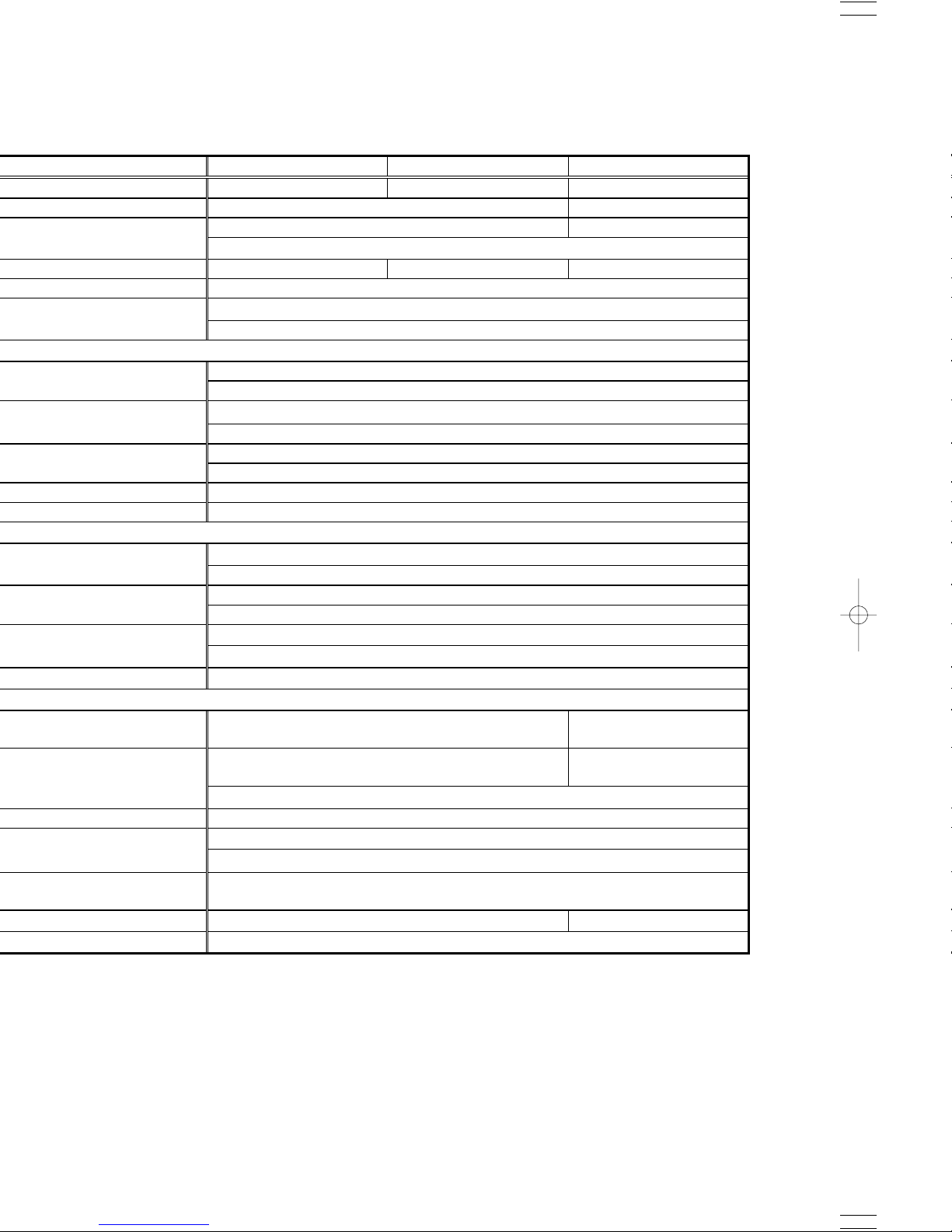
SPECIFICATIONS
IT EM S A Channel B Ch
annel
C Channel D Channel
0 t o V
0 t o 1818 V
0 to +8 V
0 t o 6 V
10 mV 1 mV
± ( 0. 5% S E T +2 0 mV ) ± ( 0. 5% S ET +5 mV )
At 23 ±5 af ter 30 minut e ag ing
0 t o +1 .8 A
0 t o 1.8 A
0 to +2 A
0 t o 1 A
1 mA
± ( 1% SET +5 mA )
At 23 ±5 after 30 m inute aging
1 mV
( For ± 10% variat ion of s
ource
voltage)
2 mV
(( For 0 to 100% variat ion )
0.5 mV
Measured in t he RMS method using 5 H z to 1 MH z signals .
µs
( typ. )
ppm/
at rate d output voltage )
2 mA
( For ± 10% variat ion of s ourc e v olta ge)
5 mA
( For 0 to 100% variat io n )
1.5 mA
Measured in the RMS method using 5 Hz to 1 MHz
signals.
15
0 ppm/ ( at rate d output current )
4 digit red LEDs, lowest digi t:
10 mV
4 digit red LEDs, lowest digit:
1 mV
± ( 0. 5% rdg + 2 0 mV )/ 10 mV ± ( 0. 5% rdg + 5 mV )/ 1 mVVoltage indication
accuracy
accuracy
At 23 ± 5 af ter 30 minute aging
4 digi t red LEDs, lowest digit: 1 mA
±( 1% rd g + 5 mA )/ 1 mA
At 23 ± 5 af ter 30 minute aging
indication
2.5% FS to +102.5% FS /0% FS to +102.5% FS
+-
-
-
-
-
ı
ı
ı
ı
ı
ı
-
-
-
-
-
-

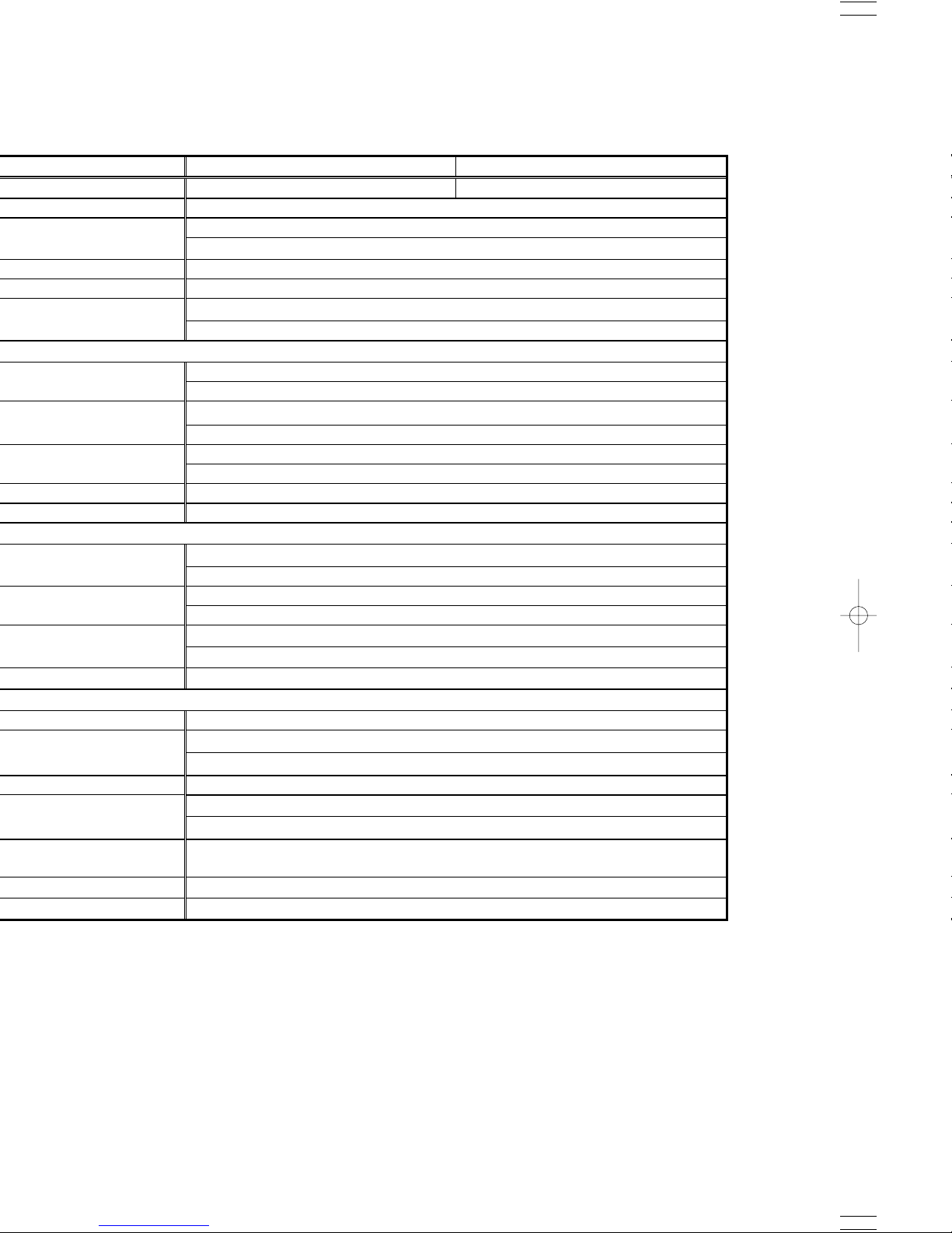
SPECIFICATIONS
ITEMS A Channel Channe Channel
0 to +1 8 V 0 to 18 V 0 to +6 V
10 m V 1 mV
± ( 0. 5% S E T +2 0 m V ) ± ( 0. 5% SET +5
mV )
At 23 ± 5 af ter 30 minute aging
1 mA
± ( 1% SET + 5 mA )
At 23 ± 5 af ter 30 minute a ging
1 mV
( For ± 10% variat ion of source voltage)
2 mV
( For 0 to 10 0% variat io n )
0.5 mV Ripple noise
Measured in the RMS method using 5 Hz to 1 MHz signals .
50 µs ( typ. )
60 ppm/ ( at rated output voltage )
2 mA
( For ± 10% variat ion of s ourc e v oltage)
5 mA
( For 0 to 10 0% variat ion )
1.5 m A
Measured in the RMS method using
5 H z t o 1 MHz
signal s.
150 ppm/ ( at rate d output current )
4 digit red LEDs,
lowest digit: 1 mV
± ( 0. 5% rdg + 2 0 mV )/ 10 mV ± ( 0. 5% rdg + 5
mV )/ 1 mV
indication
accura c y
accura c y
At 23 ±5 af ter 30 minute aging
±( 1% rdg + 5 mA )/ 1 mA Curre nt
At 23 ±5 af ter 30
2.5% FS to +102 .5% FS /0% FS to +102.5%
Common Independent
Approx . 2 00 W , 255 VA
BC
indication
-
-
-
-
ı
ı
ı
ı
ı
ı
-
-
-
-
minute aging
-
-
PW-A
5
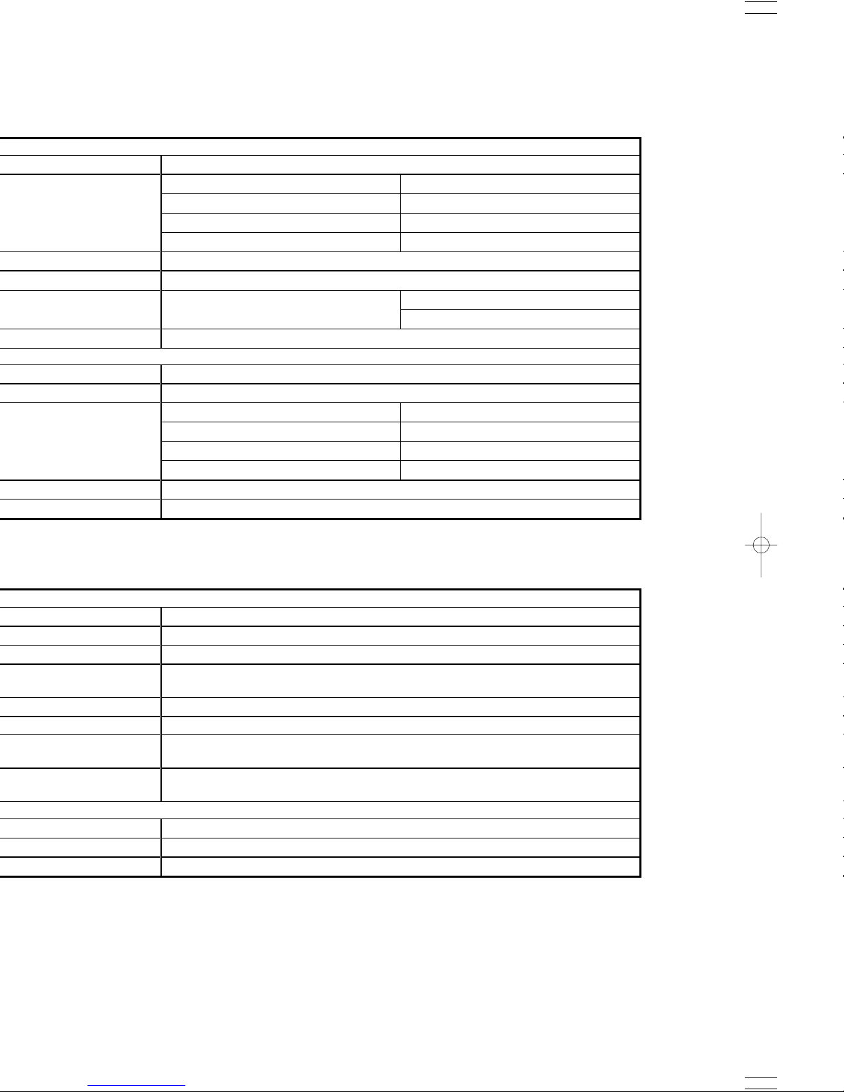
SPECIFICATIONS
0 to +18 V 0 to 18 V
mV
± ( 0.5% SET +2 0 mV )
At 23 ± 5 af ter 30 minute aging
0 to +3 A 0 to 3 A
1 mA
± ( 1% SET + 5 mA )
At 23 ± 5 af ter 30 minute aging
1 mV
( For ± 10% variat ion of s ourc e voltage)
2 mV
( For 0 to 10 0% variat io n )
0.5 m V
Measure d in t he RMS method using 5 Hz to 1 MHz signals .
50 µs ( typ. )
60 ppm/ (at rated output vo lta ge )
2 mA
( For ± 10% variat ion of source voltage)
5 mA
( For 0 to 100% va riation )
1.5 mA
Measured in the RMS method using 5 Hz to 1MHz
signals.
ppm/ ( at rate d output c urre nt )
4 dig it r ed LEDs , l o wes t d igit: 1 0 mV
± ( 0. 5% rdg + 2 0 mV )/ 10 mV
At 23 ±5 after 30 minute aging
4 digit r ed LEDs, low est di gi t: 1 mA
±( 1% rdg + 5 m A )/ 1 mA
At 23 ±5 after 30 minute aging
2.5% FS to +102 .5% FS /0% FS to +102.5%
Approx . 2 15 W , 274 VA
ITEMS
ChannelA
ChannelB
10
accura c y
indication
accura c y
indicatio
ı
ı
ı
ı
ı
ı
-
-
-
-
150
-
-
-
-
-
Common
SPECIFICATIONS
0 to +36 V 0 to 36 V
mV
± ( 0.5% SET +2 0 mV )
At 23 ± 5 af ter 30 minute aging
0 to 0 to 1.5 A
1 mA
± ( 1% SET + 5 mA )
At 23 ± 5 af ter 30 minute aging
1 mV
( For ± 10% variat ion of s ourc e voltage)
2 mV
( For 0 to 10 0% variat io n )
0.5 m V
Measure d in t he RMS method using 5 Hz to 1 MHz signals .
50 µs ( typ. )
60 ppm/ (at rated output vo lta ge )
2 mA
( For ± 10% variat ion of source voltage)
5 mA
( For 0 to 100% va riation )
1.5 mA
Measured in the RMS method using 5 Hz to 1MHz
signals.
ppm/ ( at rate d output c urre nt )
4 digit r ed LEDs, l o wes t d igit: 1 0 mV
± ( 0. 5% rdg + 2 0 mV )/ 10 mV
At 23 ±5 after 30 minute aging
4 d igit red LED s, lowest di gi t: 1 mA
±( 1% rdg + 5 m A )/ 1 mA
At 23 ±5 after 30 minute aging
2.5% FS to +102 .5% FS /0% FS to +102.5%
Approx . 19 2 W , 250 VA
ITEMS
ChannelA
ChannelB
10
accura c y
indication
accura c y
indicatio
ı
ı
ı
ı
ı
ı
-
-
-
150
-
-
-
-
-
Common
-
1.5 A
+
PW-A
7
SPECIFICATIONS
ITEMS
ChannelA ChannelB
0 to + 18 V 0 to + 18 V
10 mV
1mA
± (0.5% SET +20mV)
(1% SET +5mA)
At 23 ± 5 after 30 - minute aging
after 30 - minute aging
0 to +3A 0 to +3A
±
At 23 ± 5
1 mV
(Fo r ± 10% v ar iat ion of source voltage)
(For 0 to 100% variation)
(For 0 to 100% variation)
2 mV
0.5 mV
Measured in the RMS method using 5 Hz to 1 MHz signals.
Measured in the RMS method using 5 Hz to 1 MHz signals.
( at rated output current)
2 m A
5 m A Load variation
1.5 mA
4 - digit red LEDs, lowest digit: 10mV
4 - digit red LEDs, lowest digit: 1mA
± ( 0. 5% rdg + 20 mV ) /10mV
At 23 ± 5 after 30 - minute aging
At 23 ± 5 after 30 - minute aging
±(1% rdg + 5mA)/ 1mA
current indication&
-2.5% FS to + 102.5% FS/0% FS to + 102.5% FS
(Fo r ± 10% va r iat i on of source voltage)
ı
ı
ı
ı
ı
ı
SPECIFICATIONS
ITEMS
0 to +3 6 V 0 to +1 8 V 0 to +8 V
10 m V 1 m V
±±
±
1 m V
2 mV
0.5 m V
50 µs ( typ. )
2 m A
5 m A
( F o r 0 to 10 0% var i at io n )
1.5 mA
Independent
ChannelA ChannelB ChannelC
current indication&
Approx. 191W, 242 VA
(0.5% SET +5mV) (0.5% SET +20mV)
At 23 ± 5 after 30 - minute aging
At 23 ± 5 after 30 - minute aging
1mA
(1% SET +5mA)
0 to +1A 0 to +2A 0 to +2A
(Fo r ± 10% va r i ati on of source voltage)
(Fo r ± 10% var i at i on of source voltage)
(For 0 to 100% variation)
Measured in the RMS method using 5 Hz to 1 MHz signals.
Measured in the RMS method using 5 Hz to 1 MHz signals.
60 ppm/ ( at rated output voltage)
150 ppm/ ( at rated output current)
4 - digit red LEDs, lowest digit: 1mA
4 - digit red LEDs, lowest digit: 10mV
4 - digit red LEDs,
lowest digit: 1mV
± ( 0. 5% rdg + 20 mV ) /10mV ± ( 0. 5% rdg + 5 mV )/1
mV
At 23 ± 5 after 30 - minute aging
At 23 ± 5 after 30 - minute aging
±(1% rdg + 5mA)/ 1mA
-2.5% FS to + 102.5% FS/0% FS to + 102.5% FS
ı
ı
ı
ı
ı
ı
PW-A
9
SPECIFICATIONS
0 t o +6 V 0 to +16 V
1 mV 10 mV
± ( 0. 5% S ET +5 mV ) ± ( 0. 5% S ET +2 0 mV )
At 23 ± 5 after 30 -
30 -
min ute agin g
0 t o +3 A 0 to +5 A
1 mA
± ( 1% SET + 5 m A )
At 23 ± 5 after minute a ging
1 m V
( For ± 10% variat ion of source voltage)
2 m V
( F o r 0 to 100% v ariatio n )
0.5 m V
50 µs ( typ. )
60 ppm/ ( at rated o utput vo lta ge )
2 mA
( For ± 10% variat ion of source voltage)
5 m A
( F o r 0 to 100% va riat ion )
1.5 mA
150 ppm/ ( at rated ou tput c u rre nt )
± ( 0. 5% r dg + 5 m V ) / 1 m V ± ( 0. 5% r dg + 2 0 m V ) / 1 0 mV
±( 1% rdg + 5 m A ) / 1 mA
Ap prox . 2 40 W , 300 VA
ITEMS
ChannelA ChannelB
current indication&
Common
Measured in the RMS method using 5 Hz to 1 MHz signals.
Measured in the RMS method using 5 Hz to 1 MHz signals.
4 - digit red LEDs, lowest digit: 10mV4 - digit red LEDs, lowest digit: 1mV
4 - digit red LEDs, lowest digit: 1mA
At 23 ± 5 after 30 - minute aging
At 23 ± 5 after 30 - minute aging
-2.5% FS to + 102.5% FS/0% FS to + 102.5% FS
ı
ı
ı
ı
ı
ı
SPECIFICATIONS
ITEMS A Channel B Channel C Channel
±( 0.5% SET +5 mV )
±( 0.5% SET +20
mV )
At 23 ±5°C after 30-minute aging
±( 1% SET +5 mA ) Current setting accuracy
At 23 ±5°C after 30-m
inute aging
1 mV Input variation
( For ±10% variation of source voltage)
2 mV Load variation
( For 0 to 100% variation )
0.5 mV Ripple noise
Measured in the RMS method using 5 Hz to 1 MHz signals.
2 mA Input variation
( For ±10% variation of source voltage)
5 mA Load variation
( For 0 to 100% variation )
1.5 mA
Measured i n the RMS method using 5 Hz t o 1 MH z
signals.
4- digit red LEDs,
lowest digit: 10 mV
±( 0.5% rdg + 5 mV )/ 1 mV ±( 0.5% rdg +20
mV )
/ 10 mV
At 23 ±5°C after 30-minute aging
±( 1% rdg + 5 mA )/ 1 mA Current indication
At 23 ±5°C after 30-minute aging
-2.5% FS to +102.5% FS /0% FS to +102.5% FS
PW-A
11
SPECIFICATIONS
ATS is with a remote sensing terminal to C channel
ITEMS A Channel B Channel C Channel
±( 0.5% SET +20 mV ) ±( 0.5% SET +5
mV )
At 23 ±5°C after 30-minute aging
±( 1% SET +5 mA ) Current setting accuracy
At 23 ±5°C after 30-m
inute aging
1 mV Input variation
( For ±10% variation of source voltage)
2 mV Load variation
( For 0 to 100% variation )
0.5 mV Ripple noise
Measured in the RMS method using 5 Hz to 1 MHz signals.
2 mA Input variation
( For ±10% variation of source voltage)
5 mA Load variation
( For 0 to 100% variation )
1.5 mA
Measured in the RM S method using 5 Hz t o 1 MHz
signals.
4- digit red LEDs,
lowest digit: 1 mV
±( 0.5% rdg + 20 mV )/ 10 mV ±( 0.5% rdg + 5
mV )/ 1 mV
At 23 ±5°C after 30-minute aging
±( 1% rdg + 5 mA )/ 1 mA Current indication
At 23 ±5°C af ter 30-m inute aging
-2.5% FS to +102.5% FS /0% FS to +102.5% FS
SPECIFICATIONS
ITEMS A Channel B Channel
±( 0.5% SET +20 mV ) Voltage setting accuracy
At 23 ±5°C after 30-m
inute aging
±( 1% SET +5 mA ) Current setting accuracy
At 23 ±5°C after 30-m
inute aging
1 mV Input variation
( For ±10% variation of source voltage)
2 mV Load variation
( For 0 to 100% variation )
0.5 mV Ripple noise
Measured in the RMS method using 5 Hz to 1 MHz signals.
2 mA Input variation
( For ±10% variation of source voltage)
5 mA Load variation
( For 0 to 100% variation )
1.5 mA
Measured in th e RMS method using 5 Hz to 1 MH z
signals.
±( 0.5% rdg + 20 mV )/ 10 mV Voltage indication
At 23 ±5°C after 30-m inute aging
±( 1% rdg + 5 mA )/ 1 mA Current indication
At 23 ±5°C after 30-minute aging
-2.5% FS to +102.5% FS /0% FS to +102.5% FS

PW-A
13
SPECIFICATIONS
ITEMS Rating
becomes too high.
temperature.
Voltage fluctuation : ± 10%
0 to 40°C
range
-20 to +60°C
Primary - casing : 1500 VAC for 1 minute Dielectric strength voltage
Primary - secondary : 1500 VAC for 1 minute
Primary - casing & primary - secondary : 10 MΩ or more at 500
VDC
Secondary
-
casing : 5 MΩ or more at 250 VDC
Lead wires with connectors for external contact control : 1
Lead wires with sensing terminals
(PW18-1.3ATS, PW26-1ATS
only) : 2
ITEMS Specifications
voltage→10%)
Output lower than 10 V : 50 ms or less
10 V or higher output : 100 ms or less
20 mV or less
ITEMS Rating
1 V (per wire)
SPECIFICATIONS
IN/OUT pin 3 of connector J1
Start bit
1 [
bit]
[bit]
[bit]
[bit]
[bit]
[bit]
[bit]
[bit]
[V]
[V]
Date bit
7
Parity bit
1
Stop bit
1
1.5 [m]
0 : 5
Signal -flow NRZ
1 : 0
IN pins 2 & 5 of connector J1, connector J2
Start bit
1
Date bit
7
Parity bit
1
Stop bit
1
10 [m] ( between computer & IF-40RS)
Conforms to IEEE488-1978.
SH1, AH1, T6, TE0, L3, LE0, SR1, RL1, PP0, DC0, DT0, C0
when turning on power.
CR/LF + EOI
Possible to set all output conditions of units under control.
control.
response to inquiry.
Conforms to USB version 1.1.

PW-A
15
CIRCUIT DESCRIPTION
OVERVIEW OF PW -A
AC power input to the AC inlet of the CPU unit passes
through the units shown below and reaches the output
terminals.
CPU unit →Power supply unit E/6 → CPU unit → Power
transformer → Power supply unit D/6 → Power supply
unit C/6 → Amplifier unit → Power supply unit E/6
→
Output terminals
The CPU unit has an AC inlet. AC power input to the
AC inlet passes through a nois e-reducing capac itor,
protection fuse, and input v oltage selec tor switch, and
reaches the power supply unit E/6 provided with the
main switch. When the main switch is thrown, the AC
power returns to the CPU unit once and is input to the
power trans former. The AC power insulated by the
power transformer and transformed to the voltage,
which depends on the model, is rectified by t he power
supply unit D/6, smoothed by the power supply unit C/6,
controlled to the set value by the amplifier unit, and is
output through the output terminals of the power supply
unit B/6.
The PW-A power supply unit has as many routes as the
number of ouputs following the power transformer.
In addition to these units, the PW-A power supply unit
consists of power s upply unit A/6, dis play unit, and
CPU unit. The power supply unit A/6 generates power
for the internal circ uits, the display unit serves as the
interface, and the CPU unit controls the power and
executes various func tions.
The IF-40RS/GU/USB option provides the PW-A power
supply unit with remote control funct ions.
The YB option (factory option) is also av ailable. This
factory option provides the PW-A power supply unit
with quicker voltage descent when the out put is off.
With the input unit is connected with the amplifier unit,
the YB option discharges electric charge f rom the
output capacitors and lowers the v oltage quickly.
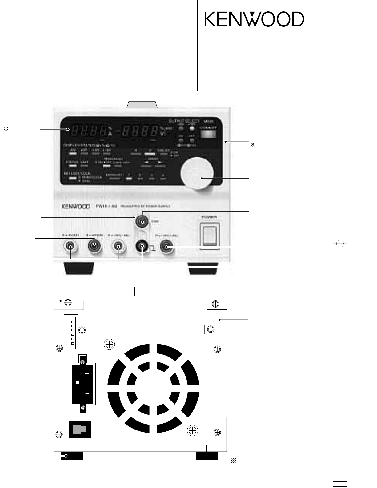
PANEL UNIT (X66-182)
(A number is a number of a block diagram)
1. Rotary encoder (S25) ---- Rotary encoder for a setup
attached to a front panel. When it turns in the direction
of a clockwise rotation, COM is cont acted in order of A
and B, and it is set t o L level. If it is an opposite
direction, it will become the order of B and A.
2. LED driver (IC1) Driver, which makes voltage
display LED turns on.
3. Voltage display LED (ED 1-4, D1) -- 7 segment LED
that displays a voltage v alue. D1 is a minus.
4. LED driver (IC2) -- Driver, which makes the current
display LED, turn on.
5. Current display LED (ED 5-8, D2) -- 7 segment LED
which displays a current value. D2 is a minus.
6. LED driver (IC3) -- LED with a switch and Driver,
which makes LED turn on
7. LED with switch (S1-12, S15-18, S21, S22, and S24)
---- LED for a display of eac h function and the switch for
a setup. LED is turned on by the driver, a switch
constitutes a matrix and scan is carried out f rom CPU.
Therefore, the switch and LED are separated in circuit .
8. Tact switch (S13, 14, 19, 20, 23) Switch for an
each setup. The matrix is const ituted with LED with
switch, and sc an is carried out from CPU.
9. Light Emitting Diode (D3-11) -- LED for each dis play.
LED which displays the beam of output and setting
change. The beam of setting change makes a voltage
and current side turns on by t he same s ignal. It is
driven by LED driver (IC3).
Details of a signal
CS* -- Data is taken in by putting in H pulse after a
serial data (16Bit) input.
DATA -- The Serial data input (16Bit)
CLK -- IC clock pulse which operates IC, the s erial data
of DATA is taken in in the st andup of this pulse.
POWER SUPPLY UNIT (X68-221)
Power supply unit X68-2210-xx is divided into six of AF, and each has another function. Moreover, PC boards
of PW16-5ADP differ for the circuit composit ion
different from other models, and PW16-5ADP becomes
X68-2300-xx.
(A number is a number of a block diagram)
X68-2210(2300)-xx A/6
The unit which makes the power supply for int ernal
circuits.
1. Rectification, flat and smooth circuit -- It rectifies
and carries out flat and smooth the power supply used
by the digital system used in a CPU unit.
The voltage after being flat and smooth is about DC9V.
2. Regulation circuit
-- The output of the above 1 is
regulated to DC5V.
The consumption current in a CPU
unit is about 350mA, when IF unit is connected, it is
about 450mA.
3. Rectification, flat and smooth circuit -- It rectifies
and carries out flat and smooth the power supply used
by CH1 and 2 side among the power supplies of the
analog system used in an amplifier unit. The voltage
after being flat and smooth is about DC±17V. In AQ,
the power supply system here is used for 4CH(s) for
the same COM. ±12V is regulated in an amplifier unit.
4.
Regulation circuit -- The output of t he above 3 is
regulated to DC±5V.
Consumption current is about
200mA, respectively.
5. Rectification, flat and smooth circuit -- It rectifies
and carries out flat and smooth the power supply used
by CH3 and 4 side among the power supplies of the
analog system used in an amplifier unit. The voltage
after being flat and smooth is about DC ±17V.
(modification 02 to 04 and 08, X68-2300-00 are no
used) ±12V is regulated in an amplifier unit.
6. Regulation circuit
-- The output of the above 5 is
regulated to DC ±5V.
Consumption current is about
200mA, respectively. (modificat ion 02 to 04 and 08,
X68-2300-00 are no used)
7. Regulation circuit
-- Power supply±12V used in t he
circuit of 8 t o 12 are made. For power consumption, 12V are about 30 to 40mA. +12 is about 10mA.
8. Heat detection circuit -- The heat of an exhaust gas
is detected with t he thermistor of TH101
9. OHA signal generating circuit -- If a fixed value wit h
CIRCUIT DESCRIPTION
It is the transistor which regulate the
A, B, C, COM1, COM2 and S attach, and a
19, 21. Positive/negativ e change -- The polarity of a
capacitor is replaced by spec code with a jumper.
X68-2210(2300)-xx D/6
13 to 16. Regulation circuit -- A bridge diode rectif ies a
main power supply. A diode and an out put become as
it is shown in the following table.
X68-2210(2300)-xxxE/6
23. The main power switch of a product is used. It
connects with a CPU unit.
X68-2210(2300)-xx F/6
24. The switch 2 which switches the input AC of a
product is used. It is used in a CPU unit as A1.
IF UNIT (X72-154)
The optional IF unit provides the PW-A power supply
unit with additional external control func tions. 0-00 is
the IF-40GU, 0-01 is the IF-40RS, and 0-02 is the IF40USB.
The CPU unit supplies +5V power.
Since these options us e the same PCBs, CN1, 2 and 3
of the GU or USB are c onnected with the CPU unit and
CN4, 5 and 6 of t he RS are connected with the CPU
unit.
(A number is a number of a block diagram)
1. CPU The CPU controls the interfaces . The CPU
unit supplies power source and clock puls es. This is
connected with the CPU of the CPU unit through the
buffer and bus transceiver s hown in 2 and executes
communication with the PW-A unit.
2. Buffer and bus transceiver The buffer and bus
transceiver connect the CPUs of the PW-A unit and IF
unit. They connect the CPU when the PW-A unit
00 01,09 02 03
A
OUTPUTAOUTPUTAOUTPUTAOUTPUT
B
OUTPUTBOUTPUTBOUTPUTBOUTPUT
C
OUTPUTCOUTPUT
D
OUTPUTCOUTPUT
04 05 06 07,11
A
OUTPUTAOUTPUTAOUTPUTAOUTPUT
B
OUTPUTBOUTPUTBOUTPUTBOUTPUT
C
OUTPUTCOUTPUTCOUTPUT
C
OUTPUTCOUTPUT
08 X68-2300
±
±
08 X68-2300
D401
A OUTPUT
A OUTPUT
D402
B OUTPUT
B OUTPUT
D403
B OUTPUT
D404 B OUTPUT
D401
C
00 01 02 03
OUTPUTCOUTPUTAOUTPUT
D402
D
OUTPUTCOUTPUTBOUTPUT
B
OUTPUT
D403
A
OUTPUTAOUTPUT
A
OUTPUT
D404
B
OUTPUTBOUTPUT
D401
A
04 05 06 07,11
OUTPUTCOUTPUTCOUTPUTCOUTPUT
D402
B
OUTPUT
C
OUTPUT
C
OUTPUT
B
OUTPUT
D403
A
OUTPUTAOUTPUTAOUTPUT
D404
B
OUTPUTBOUTPUT

PW-A
17
CIRCUIT DESCRIPTION
communica-
socket
started using
copy program is
program in this ROM
power supply unit.
Channels 2 and 4 use the COM commonly . In a threechannel power supply unit, channels 1 and 2 use a
different common line from channel 3. Thus, the power
lines are different.
Since the circuit configurat ion is identical, the
description below explains channel 1.
(A number is a number of a block diagram)
1. D/A converter (I C2) (CH2: IC1, CH3: IC20, CH4:
IC19) The D/A converter receives digit al signal
indicating the set value from the CPU unit and converts
it into an analog s ignal. The PCM1700U, a DAC unit
used, has two circuits, which convert the CVREF
volt age and CCREF v olt a ge, re s pec t iv e ly .
The D/A converter outputs approximately 0 to -2.25 V
through pins 16 and 27, regardles s of the output on/ off
condition.
2. REF (non) reversing circuit (IC3 and IC4) This
circuit amplifies t he output voltage of the D/A converter
by reversing or not reversing it ac cording to its polarity.
Channel 1 uses all of 00 to 09 as two reversing
amplifiers to provide non-reverse output. CV REF is
output through pin 1, and CC REF is output through pin
7. The voltage is
approximately 0 to -7.5 V.
3. CC error amplifier (IC8-1/2)
This amplifier compares the CC REF output (B) of the
REF (non) reversing circuit with the output (D) of the
current detector circuit and amplifiers the error to
control the power transistors in CC operation.
4. CV error amplifier (IC8-2/2)
This amplifier compares the output (C) of the REF (non)
reversing circuit with the output voltage sensing v alue
(E) and amplifiers the error to control the power
transistors in CV operation. This amplifier ORs the
outputs shown in 3 and 4 and always use either output
to control the power transistors shown in 5 below.
5. Power transistors (First st age: Q4, 5 and 6, final
stage: Q1, 2 and 3) (CH2 … First st age: Q10, 11 and
12, final stage: Q7, 8 and 9. CH3 … First st age: Q15
and 16, final stage: Q13 and 14. CH4 … First stage:
Q19 and 20, final stage: Q17 and 18.)
These are the main power transistors for stabiliz ing the
output power. Two trans istors are Darlington-
connected.
The number and characteristics of the
power transistors
differ with the output specif ications.
6. Current detection circuit (R41 and IC11) The fourterminal resistor R41 detects the output current, which
is input to the differential amplif ier (IC11 1/2), reversed
by a buffer and input into the CC error amplifier shown
in 3. Since the voltage must be posit ive when
monitoring
the current, positive power does not pas s
through the
reversing buffer and is input to t he signal
selector shown
in 9. Negative power is reversed by
the reversing buff er.
7. Voltage monitor circuit (IC10 2/2)
This circuit attenuates t he output v oltage A and
produces a voltage monitoring signal.
8. OUT ON/OFF (Q21 OR Q22)
This circuit makes the base s ignal of the power
transistors and CV/CC REF into posit ive or negative
voltage according t o the CPU and stops the output.
Parts and voltage dif fer with the polarity of the output.

CIRCUIT DESCRIPTION
CPU, ROM, RAM and so forth, AC inlet, fus e, input
selector switch, and AC power supply unit with
capacitors.
The digital control circuit reads signals of the rot ary
encoder and switches from the display unit connected
with a flat c able and s ends control data t o the amplifier
unit.
The AC power supply unit feeds power input into the AC
inlet to the transformer through the power supply unit
E/6 with a power switch.
The amplifier unit supplies +5 V.
Digital control circuit
(A number is a number of a block diagram)
1. CPU (I C1): Microcomputer IC. Clock frequency :
12.2 MHz. Driven on +5 V. Executes various controls.
2. Reset circuit (IC11): This circuit monitors +5 V
when power is turned on, changes the RESET signal
level from L into H, and activates the CPU. It als o
gives a latch enable s ignal of the OUTPUT signal in
order to prevent output when the power source is
unstable.
3. Line decoder (IC6) and data latch (IC7, 8, 9, and 10):
These convert the data line data into eac h data.
4. EEPROM (IC4 and 5): An I C for storing the power
setting, adjustment values , etc.
5. Isolation (PH1 to 29): Isolates the digital circuit s
from the analog circuits .
S-DATA -- Serial data of the set voltage and current.
Connected to the DAC of the amplifier unit. The
reference signal is produced based on this data.
CLK-DA -- Clock pulses for the above serial dat a
LE-DA -- Latch enable signal for the above serial data.
Transferred to the converter synchronous ly with the
trailing edge.
CLK-CTR -- Clock pulses to the shift register of the
amplifier unit. The S DATA shown above is us ed.
LE-CTR -- Latch enable signal to the shift register of
the amplifier unit. Analog data to be supplied to the
ADC is selected according to t he shift register.
DATA-AD -- Serial data from the ADC of t he amplifier
unit. This data is read and the out put value is
displayed.
CS-AD -- Select signal t o the ADC. The ADC is in the
sleep condition when this s ignal is Low.
CLK-AD -- Clock pulses to the ADC. Data is read
using this cloc k pulse f or external clock operation.
OUT -- OUTPUT ON/OFF signal to eac h channel.
CVCC -- This signal indicates the CV/CC operation
condition of each channel. It is s ent by the amplifier
unit and read by the CPU, which reflec ts t he signal
upon the display unit.
6. Encoder signal (IC…): When the encoder is rotated
clockwise, pin 5 of IC12 outputs a High signal and pin 9
of IC12 outputs a Low signal. When the encoder is
rotated counterclockwise, pin 5 of IC12 outputs a Low
signal and pin 9 of IC12 outputs a High s ignal. IC14-2
goes Low and an int errupt signal is input to the CPU
when either operation is carried out. The CPU reads
and clears this s ignal.

PW-A
19
CIRCUIT DESCRIPTION
7. External control (CN..) These are directly connected
protection.
output. PH30 is
CN5-1 -- The MAIN OUTPUT is t urned on when this
terminal goes Low.
CN5-2 -- The voltage and current set values change
into the PRESET4 values when this terminal goes Low.
CN5-3 -- The voltage and current set values change
into the PRESET3 values when this terminal goes Low.
CN5-4 -- The voltage and current set values change
into the PRESET2 values when this terminal goes Low.
CN5-5 -- The voltage and current set values change
into the PRESET1 values when this terminal goes Low.
CN5-7 -- The MAIN OUTPUT is turned off when this
terminal goes Low. I t goes Low when the OHA
condition is established.
AC power supply circuit
8. J1: AC inlet
A1 -- A switch for changing t he input AC voltage
CN11 -- Fuse holder
C38 to 41 -- Noise-reducing capacitors

PW-A
20
BLOCK DIAGRAM
PW-A
A double arrow is the flow of an input to an output. A dotted line portion is a primary side inside.
CPU UNIT (X77-2380-xx)
• CPU CIRCUIT
• ExtCont TERMINAL
• AC INPUT TRANSFER
• IN PUT PROTECTION
FUSE
PANEL UNIT
(X66-1820-xx)
• DISPL AY LED
• OPERATION SYSTEM
SWITCH
• ROTARY ENCODER
±DC OUT
AC IN
POWER SUPP LY UNIT
(X68-2210-xx B/6)
MAIN OUTPUT
TERMINAL
AMP UNIT
(X73 -2320-xx)
• D/A, AD
CONVERTING
• REF VO LT AGE
• AN ALOG CONTROL
CIRCUIT
• POWER
TRANSISTOR
POWER
TRANSFORMER
POWER SUPP LY UNIT
(X68-2210-xx A/6)
• INTERNAL CIRCUIT
POWER SUPPLY
IF -40GU/RS/USB
DC FAN
OPTION FOR INTERFACE UNIT
Y87-xxxx -xx
POWER SUPP LY
UNIT
(X68-2210-xx D/6)
• RECTIFICATION
CIRCUIT
POWER SUPP LY
UNIT
(X68-2210-xx C/6)
• SMOOTHING
CIRCUIT
1324
On output terminal, a number
changes model.
The power supply of CPU and
PANEL UNIT is supplied via
an amplifier unit.
POWER SUPP LY
UNIT
(X68-2210-xx E/6)
POWER SWITCH
OPTION YB OPTION
Y87-xxxx -xx
X72-1620-xx
X72-1540-xx
OP-19A ~ G
∗
PW-A
21
BLOCK DIAGRAM
X66-1820-xx
1. ROTARY
ENCODER
S25
2. LED
DRIVER
IC1
3. LED
VOLTAGE DISPLAY
ED1 ~ 4, D1
4. LED
DRIVER
IC2
5. LED
CURRENT DISPLAY
ED5 ~ 6, D2
6. LED
DRIVER
IC3
7. LED WITH SWITCH
S1 ~ 12, S15 ~18, S21, S22,. S24
8. TACT SWITCH
S13, 14, 19, 20, 23
9. LED
D3 ~ 11
R/E A, R/E B
CS0
CLK, DATA
CS2
CS1
ED1**
ED2**
LED**
KEY0 ~ 2
KEYD ATA0 ~ 7
CPU UNIT
X77-2380-xx
CN8,9,10
PW-A
22
BLOCK DIAGRAM
X68-2210-xx
POWER TRANSFORMER
1. RECTIFICATION
SMOOTING CIRCUIT
D101, C102
2. REGUL ATOR
CIRCUIT
IC101
X73-2320-xx AMP UNIT
3. RECTIFICATION
SMOOTING CIRCUIT
D102, C104, C105
4. REGUL ATOR
CIRCUIT
IC102, 103
5. RECTIFICATION
SMOOTING CIRCUIT
D103, C107, C108
6. REGUL ATOR
CIRCUIT
IC104, 105
X68-2210-xx A/6
10. RECTIFIC ATION
SMOOTING CIRCUIT
D104, D105, C109
11. TRANSISTOR
Q101
12. ERROR AMPLIFICATION
CIRCUIT
IC106 -2/2, R107, 108, 109, 110
DC
FAN
7. REGUL ATOR CIRCUIT IC107, D108
8. HE AT DETECTION
CIRCUIT
TH101
9. OHA SIGNAL
GENER ATING CIRCUIT
IC106
X73-2320-xx AMP UNIT
OUTPUT TERMINAL
OUTPUT TERMINAL
(COM2) OUTPU T TERMINAL
(D) OUTPUT TERMINAL
TERMINAL
X68-2210-xx B/6
-S
+S
OUTPUT TERMINAL
OUTPUT TERMINAL
OUTPUT TERMINAL
OUTPUT TERMINAL
TERMINAL
X68-2300-xx B/6
-S
+S
B
2
C
O
M
2
C
O
M
A
B
C
O
M
A
B
C
D
 Loading...