

Kenwood NXR-810, NXR-810C Service Manual
UHF DIGITAL BASE-REPEATER / UHF
NXR-810
数字模拟双模中继台
SERVICE MANUAL /
C version / C
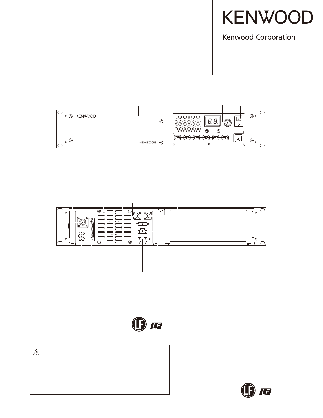
Antenna cable (TX OUT)
天线电缆(发射输出)
(E30-7528-15)
Rear panel
后面板
(A82-0077-02)
版本
Front panel
前面板
(A62-1174-03)
Blade fuse (15A/32V)
刀片式保险丝(15A/32V)
(F05-1537-05)
Antenna cable (REF IN)
天线电缆(基准输入)
(E30-7690-05)
维修手册
Key top / 按键
(K29-9370-02)
Antenna cable (RX IN)
天线电缆(接收输入)
(E30-3418-15)
© 2010-5 PRINTED IN CHINA
B51-8924-00 (N)
Knob (Volume)
旋钮(音量)
(K29-5389-03)
CH/STATUS
TX
VOLUME
BUSY
Knob (Power)
旋钮(电源)
(K29-9106-04)
POWER
MIC
Modular jack
模块化插孔
(E58-0522-05)
TX OUT
CONTROL
I/O
TEST/SPKR
Lead wire with connector
(DSUB25P)
带有连接器的导线(DSUB25P)
(E37-1376-05)
Lead wire with connector
(ACC15P)
带有连接器的导线(ACC15P)
(E37-0913-05)
REF IN RX IN
Modular jack x 2
模块化插孔 x 2
(E58-0533-05)
无铅焊接通信产品
保护环境建伍领先
注意∶本产品是无铅化焊接产品
在维修时请使用无铅焊锡
FUSE
DC 13.6V
N SYNC
DC cord (Ext DC in)
直流电源线(外部直流输入)
(E30-3414-05)
和相应的焊接工具
详细事项请访问如下网址了解:
This product complies with the
http://www.kenwoodhk.com.hk/
directive for the European market.
RoHS
This product uses Lead Free solder.

NXR-810
CONTENTS /
GENERAL .....................................................3
SYSTEM SET-UP .........................................4
REALIGNMENT ...........................................5
OPERATING FEATURES .............................8
INSTALLATION ..........................................10
MODIFICATION .........................................13
DISASSEMBLY FOR REPAIR ....................16
CIRCUIT DESCRIPTION ............................17
COMPONENTS DESCRIPTION .................32
PARTS LIST ...............................................36
EXPLODED VIEW ......................................52
PACKING ....................................................54
TROUBLE SHOOTING ..............................55
ADJUSTMENT ..........................................64
TERMINAL FUNCTION .............................92
PC BOARD
FINAL UNIT (X45-3932-71) .................108
CONTROL UNIT (X53-4490-10) ..........112
DISPLAY UNIT (X54-3730-20) .............116
TX-RX UNIT (X57-7952-71) .................120
RX VCO/PLL UNIT (X58-5090-10) ......124
TX VCO/PLL UNIT (X58-5100-10) ......125
INTERCONNECTION DIAGRAM ............126
SCHEMATIC DIAGRAM ..........................128
BLOCK DIAGRAM ...................................146
OPTIONAL ACCESSORIES
KES-5 (EXTERNAL SPEAKER) ............149
SPECIFICATIONS ....................................150
目录
概 述 ........................................................................ 3
系统体系 ........................................................................ 4
模式组合 ........................................................................ 5
操作特性 ........................................................................ 9
安 装 ......................................................................10
改 装 ......................................................................13
维修拆卸 ......................................................................16
电路说明 ......................................................................17
元件说明 ......................................................................32
零 件 表 ......................................................................36
部件分解图 .................................................................52
包 装 ......................................................................54
故障排除 ......................................................................56
调 整 ......................................................................65
端子功能 ......................................................................93
PC 板
末级单元 (X45-3932-71) ............................ 108
控制单元 (X53-4490-10) ............................ 112
显示单元 (X54-3730-20) ............................ 116
TX-RX 单元 (X57-7952-71) ...................... 120
RX VCO/PLL 单元 (X58-5090-10) ........124
TX VCO/PLL 单元 (X58-5100-10) ........125
互 连 图 ...................................................................126
原 理 图 ...................................................................128
方 块 图 ...................................................................146
可选附件
KES-5( 外部扬声器 ) ..................................... 149
规 格 ................................................................... 151
Document Copyrights
Copyright 2010 by Kenwood Corporation. All rights re-
served.
No part of this manual may be reproduced, translated,
distributed, or transmitted in any form or by any means,
electronic, mechanical, photocopying, recording, or otherwise, for any purpose without the prior written permission
of Kenwood.
Disclaimer
While every precaution has been taken in the preparation
of this manual, Kenwood assumes no responsibility for errors or omissions. Neither is any liability assumed for damages resulting from the use of the information contained
herein. Kenwood reserves the right to make changes to any
products herein at any time for improvement purposes.
2
文档版权信息
Kenwood Corporation 拥有版权 2010。保留所有权利。
未经Kenwood 公司预先书面同意,无论出于何种目的,均
不得以任何形式或任何方式包括电子、机械、影印、录音或
其他方式复制、翻译、分发或传播本手册的任何部分。
免责声明
Kenwood 公司在准备本文档时已采取所有必要的预防措施,
恕不对错误或疏漏承担任何责任,也不对因使用本文中所含
的信息而导致的损害负责。Kenwood 公司保留出于改进的需要
而随时对文中的产品信息做出更改的权利。

NXR-810
GENERAL /
INTRODUCTION
SCOPE OF THIS MANUAL
This manual is intended for use by experienced technicians familiar with similar types of commercial grade communications equipment. It contains all required service
information for the equipment and is current as of the publication date. Changes which may occur after publication
are covered by either Service Bulletins or Manual Revisions.
These are issued as required.
ORDERING REPLACEMENT PARTS
When ordering replacement parts or equipment information, the full part identifi cation number should be included.
This applies to all parts: components, kits, or chassis. If the
part number is not known, include the chassis or kit number
of which it is a part, and a suffi cient description of the required component for proper identifi cation.
PERSONAL SAFETY
The following precautions are recommended for personal
safety:
• DO NOT transmit if someone is within two feet (0.6 me-
ter) of the antenna.
• DO NOT transmit until all RF connectors are secure and
any open connectors are properly terminated.
• SHUT OFF this equipment when near electrical blasting
caps or while in an explosive atmosphere.
• All equipment should be properly grounded before pow-
erup for safe operation.
• This equipment should be serviced by only qualifi ed tech-
nicians.
概述
引言
本手册的范围
本手册是提供给熟悉通信专业并且具有维修经验的技术人
员使用的。它包括了维修该设备所需要的全部资料和现行出
版日期。在出版后可能发生变动,如果需要,可以参照《维
修通报》或《手册修订本》进行补充。
替换零件的订购
当订购替换零件或设备资料时,应注意完整的零件识别号
码。所有的零件均有识别号码∶元件,组件或机壳。如果不
知道零件的号码,为了正确地识别,必须注明此元件所属的
机壳或组件的号码,并对元件进行充分的说明。
个人安全
为了个人的安全,请注意下列事项∶
• 如果有人在天线两英尺 (0.6 米 ) 范围之内时,不要进行发
射。
• 在没有认真核实所有射频插头之前或有任何一个脱开的插
头没有连接到相应端口上的情况下均不要发射。
• 在电爆管附近或在易燃性气体环境中,必须关闭电源,不
要操作本设备。
• 为了操作的安全,在接通电源之前所有设备应该连接地线。
• 本设备只应该由有资格的技术人员进行维修。
SERVICE
This transceiver is designed for easy servicing. Refer to
the schematic diagrams, printed circuit board views, and
alignment procedures contained within.
维修服务
为了便于维修本设备,建立了完整的维修服务体系,提供
了包括原理图,印刷电路板图和调整步骤在内的资料供参考。
3
NXR-810
SYSTEM SET-UP /
Merchandise received
Choose the type of transceiver
Repeater programming & setup
DC power supply or
duplexer?
NO
External speaker?
NO
Delivery
系统体系
Frequency range RF power Type
TX/RX 400~470MHz 40W C
See page 5.
A personal computer, programming interface (KPG-46/46A), and
programming software (KPG-129D(C)) are required for programming.
YES
YES
Installation in the optional space
(Option)
KES-5 installation
(Option)
See page 11.
See page 10.
接收订单
选择
中继台
的类型
中继台编程与设置
DC电源或双工器?
否
外部扬声器?
否
交货
频率范围 射频功率 类型
TX/RX 400~470MHz 40W C
参见第5页。
需使用个人电脑,编程接口(KPG-46/46A)和编程软件(KPG-129D(C))进行编程。
是
是
在可选空间内安装
KES-5的安装
(
可选件
(
可选件
参见第11页。
)
参见第10页。
)
4

NXR-810
REALIGNMENT /
1. Modes
User mode
PC mode
Firmware programming mode
Mode Function
User mode Use this mode for normal operation.
PC mode
PC programming
mode
PC test mode
Firmware programming mode
PC programming mode
PC test mode
Use this mode to make various settings by
means of the FPU through the RS-232C
port.
Use to read and write frequency data and
other features to and from the repeater.
Use to check the repeater using the PC.
This feature is included in the FPU.
Use when changing the fi rmware program
of the fl ash memory.
PC tuning mode
模式组合
1. 模式
用户模式
PC模式
固件编程模式
模 式 功 能
用户模式 用此模式进行一般操作。
PC 模式
PC 编程模式
PC 测试模式
固件编程模式 更改闪存的固件程序时使用。
PC编程模式
PC测试模式
用此模式通过 RS-232C 端口利用 FPU 进行各
种设置。
用于将频率数据及其它功能写入到中继台或
从中继台读取。
用于通过 PC 检查中继台。
该功能内置于 FPU 中。
PC调谐模式
2. How to Enter Each Mode
Mode Operation
User mode Power ON
PC mode Received commands from PC
Firmware programming mode [PF1] + Power ON (one second)
3. PC Mode
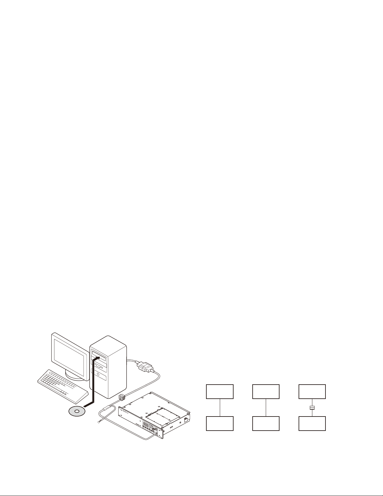
3-1. Preface
The NXR-810 is programmed by using a personal computer, programming interface (KPG-46/46A) and programming
software (KPG-129D(C)).
The programming software can be used with a PC. Figure
1 shows the setup of a PC for programming.
3-2. Connection Procedure
1. Connect the NXR-810 to the computer using the interface
cable and USB adapter (When the interface cable is KPG-
46A, the KCT-53U can be used.).
Note:
• You must install the KCT-53U driver in the computer to
use the USB adapter (KCT-53U).
• When using the USB adapter (KCT-53U) for the first time,
plug the KCT-53U into a USB port on the computer with
the computer power ON.
2. 如何进入每一种模式
模 式 操 作
用户模式 接通电源
PC 模式 从 PC 接收指令
固件编程模式 [PF1]+ 接通电源 (1 秒钟 )
3. PC 模式
3-1. 前言
NXR-810 采用个人电脑、编程接口 (KPG-46/46A) 和编程软
件 (KPG-129D(C)) 进行编程。
编程软件可在 PC 上使用。图 1 说明了 PC 进行编程的设置。
3-2. 连接操作
1. 用接口电缆和 USB 适配器将 NX R -810 连接到电脑 ( 接口电
缆为 KPG-46A 时,可以使用 KCT-53U)。
注意 :
· 必须在电脑上安装 K C T -53U 驱动程序才能使用 U S B 适配器
(KCT-53U)。
· 首次使用 U SB 适配器 (KCT-53U) 时,请在电脑电源打开的
情况下将 KCT-53U 插入电脑的 USB 端口。
5
NXR-810
REALIGNMENT /
2. When power is applied, the user mode is entered immediately. When the PC sends a command, the repeater
enters the PC mode and displays “PC” on the 7-segment
LED. When data is being transmitted to the PC from the
repeater, the TX LED flashes. The BUSY LED flashes
when data from the PC is being received by the repeater.
Note:
• The data stored in the personal computer must match the
model type, when it is written into the fl ash memory.
• Change the NXR-810 to PC mode, then attach the interface cable.
3-3. KPG-46/KPG-46A Description
(PC programming interface cable: Option)
The KPG-46/46A is required to interface the NXR-810 to
the computer. It has a circuit in its D-sub connector (KPG46: 25-pin, KPG-46A: 9-pin) case that converts the RS-232C
logic level to the TTL level.
The KPG-46/46A connects the 8-pin microphone connec-
tor of the NXR-810 to the RS-232C serial port of the computer.
模式组合
2. 接通电源时,即可进入用户模式。PC 发出指令时,中继
台进入 PC 模式并在 7 段 LE D 上显示“P C”。当数据从中继
台传送到 P C 时,T X L E D 闪烁。中继台接收 P C 的数据时,
BUSY LED 闪烁。
注意 :
· 个人电脑储存的数据写入闪存时,必须与机型相符。
• 将 NXR-810 改为 PC 模式,然后连接接口电缆。
3-3. KPG-46/KPG-46A 说明
(PC 编程接口电缆 : 选购件 )
将 NXR-810 连接到电脑需要 KPG-46/46A。它的 D-sub 连接
器 (KPG-46:25 针 ,KPG-46A :9 针 ) 盒中有一个电路,可以将
RS-232C 逻辑电平转换为 TTL 电平。
KP G-46/46A 将 NX R-810 的 8 针麦克风连接器连接到电脑的
RS-232C 串行端口。
3-4. KCT-53U Description (USB adapter: Option)
The KCT-53U is a cable which connects the KPG-46A to a
USB port on a computer.
When using the KCT-53U, install the supplied CD-ROM
(with driver software) in the computer. The KCT-53U driver
runs under Windows 2000, XP or Vista (32-bit).
3-5.
Programming Software KPG-129D(C) Description
The KPG-129D(C) is the programming software for the
transceiver supplied on a CD-ROM. This software runs under Windows XP, Vista or 7 on a PC.
The data can be input to or read from the NXR-810 and
edited on the screen. The programmed or edited data can
be printed out. It is also possible to tune the NXR-810.
PC
(KPG-46 or KPG-46A or KPG-46A + KCT-53U) + Tuning cable (E30-3383-05)
(KPG-46或KPG-46A或KPG-46A + KCT-53U) + 调谐电缆(E30-3383-05)
NXR-810
KPG-129D(C)
3-4. KCT-53U 说明 (USB 适配器 : 选购件 )
KCT-53U 是将 KPG-46A 连接到电脑 USB 端口的电缆。
使用 K C T -53U 时,请在电脑上安装附带的 CD-ROM( 含有
驱动程序软件)。KC T-53U 驱动程序在 Windows 2000、X P 或
Vista(32 位 ) 下运行。
3-5. 编程软件 KPG-129D(C) 说明
KPG-129D(C) 是 CD-ROM 附带的用于中继台的编程软件。该
软件在 PC 的 Windows XP、Vista 或 7 下运行。
可向 N X R-810 写入或读取数据,并可在屏幕上进行编辑。
可以打印编程或编辑的数据。此外,还可调谐 NXR-810。
PC
D-SUB
(25-pin/25针)
KPG-46
Transceiver
中继台 中继台 中继台
PC
D-SUB
(9-pin/9针)
KPG-46A
Transceiver Transceiver
PC
USB
KCT-53U
KPG-46A
Fig. 1 /
图1
6

NXR-810
REALIGNMENT /
4. Firmware Programming Mode
4-1. Preface
The NXR-810 uses fl ash memory to allow it to be easily
upgraded when new features are released in the future.
4-2. Connection Procedure
Connect the NXR-810 to the personal computer using the
interface cable (KPG-46/46A) and USB adapter (KCT-53U:
when the interface cable is KPG-46A, the KCT-53U can be
used.). (Connection is the same as in the PC Mode.)
Note:
You can only program firmware from the 8-pin microphone connector on the front panel. Using the 25-pin logic
interface on the rear panel will not work.
4-3. Programming
1. Start up the firmware programming software (Fpro.exe
(ver. 4.1 or later)). The Fpro.exe exists in the KPG-129D(C)
installed folder.
2. Set the communications speed (normally, 115200 bps)
and communications port in the confi guration item.
3. Set the fi rmware to be updated by File name item.
4. Turn the NXR-810 power ON with the [PF1] key held
down. Then, “P.G.” is displayed.
5. Check the connection between the NXR-810 and the per-
sonal computer, and make sure that the NXR-810 is in the
Program mode.
6. Press “write” button in the window. When the NXR-810
starts to receive data.
7. If writing ends successfully, the TX LED on the NXR-810
lights.
8. If you want to continue programming other NXR-810s,
repeat steps 4 to 7.
模式组合
4. 固件编程模式
4-1. 前言
NXR-810 使用闪存,以便于在将来发布新功能时进行升级。
4-2. 连接操作
用接口电缆 (KPG-46/46A) 和 USB 适配器 (KCT-53U: 接口电
缆为 KPG-46A 时,可以使用 KCT-53U。) 将 NXR-810 连接到个
人电脑。( 连接方式与 PC 模式下相同。)
注意 :
您只能通过前面板的 8 针麦克风连接器对固件进行编程。
使用后面板的 25 针逻辑接口进行编程时不起作用。
4-3. 编程
1. 启动固件编程软件 (Fpro.exe(ver.4.1 或更高版本 ))。
Fpro.exe 存在于 KPG-129D(C) 安装文件夹内。
2. 在配置项中设置通信速度 ( 通常为 115200 bps)和通信端
口。
3. 通过文件名项设置要更新的固件。
4. 按住 [PF1] 键打开 NXR-810 的电源。此时 , 显示“P.G.”。
5. 检查 NXR-810 与个人电脑之间的连接,确认 NXR-810 处于
编程模式。
6. 按窗口中的写入按钮。NXR-810 开始接收数据。
7. 如果成功完成写入,NXR-810 上的 TX LED 亮起。
8. 若要继续为其他 NXR-810 编程,请重复步骤4到7。
Note:
This mode cannot be entered if the Firmware Program-
ming mode is set to Disable in the Programming software.
4-4. Function
If you press the [PF6] key while “P.G.” is displayed, the
display changes to “P G” to indicate that the write speed
is low speed (38400 bps). If you press the [PF6] key again
while “P G” is displayed, the display changes to “P G.” to
indicate that the write speed is medium speed (57600 bps).
If you press the [PF6] key again while “P G.” is displayed,
the display changes to “P.G.” to indicate that the write
speed is high speed (115200 bps).
Note:
Normally, write in the high-speed mode.
注意 :
如果编程软件的固件编程模式设为禁用,则无法进入此模
式。
4-4. 功能
如果在显示“P.G .”时按 [PF6] 键,则显示变为“P G”以
表示写入速度为低速 (38400 bps)。如果在显示“P G”时再次
按 [PF6] 键,则显示变为“P G.”以表示写入速度为中速 (57600
bps)。如果在显示“P G.”时再次按 [PF6] 键,则显示变为“P.G.”
以表示写入速度为高速 (115200 bps)。
注意 :
通常以高速模式写入。
7
NXR-810
OPERATING FEATURES
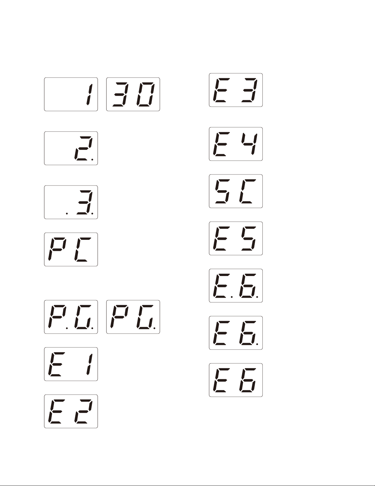
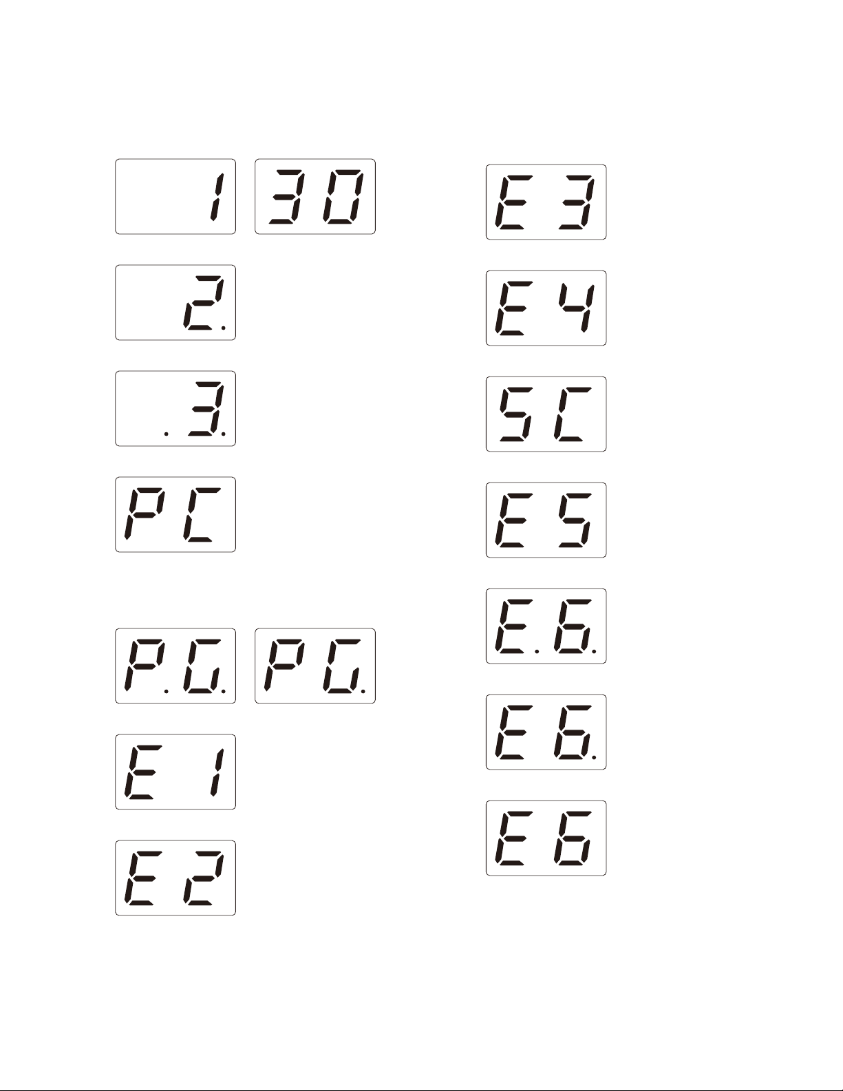
1. Two 7-segment LED Displays
• Channel display (1~30): While operating normally in user
mode.
• When the displayed channel is contained in scan sequence, the right side decimal point is displayed.
• When the displayed channel is the priority channel, the
left side decimal point is displayed.
• “PC” is displayed while in PC mode.
• “E3” is displayed when PLL is unlocked.
Receiver PLL unlocked = BUSY LED blinks.
Transmitter PLL unlocked = TX LED blinks.
• “E4” is displayed when PTT is attempted on a channel
number that has no TX frequency data programmed.
• “SC” is displayed while in scan mode.
• “E5” is ESN blank error.
• “PG” is displayed while in fi rmware programming mode.
2 decimal points displayed = 115,200 bps
1 decimal point displayed = 57,600 bps
No decimal = 38,400 bps
• “E1” is displayed when FPU data is not written.
• “E2” is displayed when the channel data is not written.
• “E.6.” is MCU internal RAM error.
• “E6.” is DSP RAM error.
• “E6” is MCU External RAM error.
8
操作特性
NXR-810
1. 两个 7 段 LED 显示
• 信道显示 (1 ~ 30): 以用户模式正常操作时。
• 显示的信道包含在扫描序列中时,显示右侧的小数点。
• 显示的信道为优先信道时,显示左侧的小数点。
• 处于 PC 模式时,显示“PC”。
• PLL 失锁时,显示“E3”。
接收机 PLL 失锁 = BUSY LED 闪烁。
发射机 PLL 失锁 = TX LED 闪烁。
• 在未编写 TX 频率数据的信道上尝试 PTT 时,显示“E4”。
• 处于扫描模式时,显示“SC”。
• “E5”表示 ESN 空白错误。
• 处于固件编程模式时,显示“PG”。
显示 2 个小数点 = 115,200bps
显示 1 个小数点 = 57,600bps
无小数点 = 38,400bps
• 未写入 FPU 数据时,显示“E1”。
• 未写入信道数据时,显示“E2”。
• “E.6.”表示 MCU 内部 RAM 错误。
• “E6.”表示 DSP RAM 错误。
• “E6”表示 MCU 外部 RAM 错误。
9
NXR-810
INSTALLATION /
1. External Speaker (KES-5)
The NXR-810 has a built-in speaker (5W/8Ω), and the external speaker output from the TEST/SPKR connector (15pin) on the rear of the radio is 4W/4Ω. Use external speaker
KES-5.
1-1. Connection for the KES-5 with the NXR-810
When taking the AF output from the TEST/SPKR
■
connector (15-pin) on the rear of the radio
The following tools are required for changing the connector.
• Extracting tool
The following extracting tool is recommended:
Molex Inc. Order No.: 11-03-0002 (W05-0878-00)
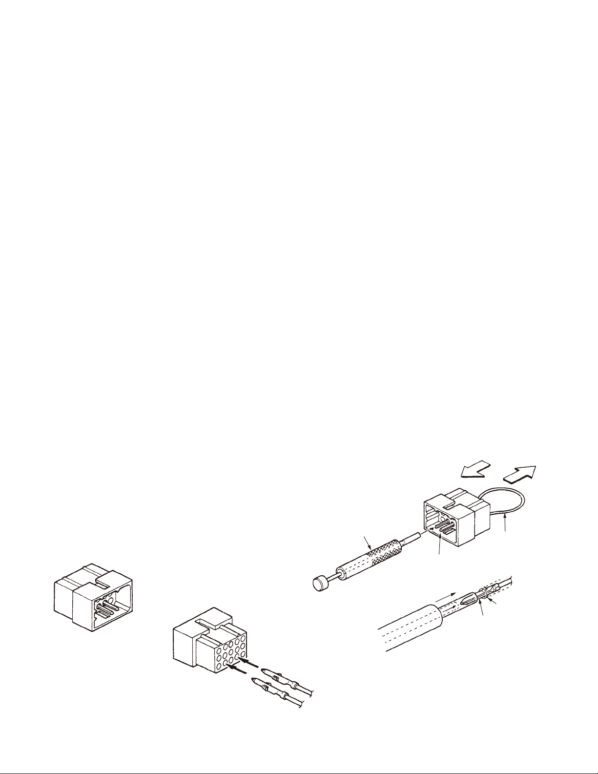
1. Remove the connector with jumper from the external
speaker connector on the rear panel of the radio. (Fig.1-1)
Note: Save the jumper, which is required when the radio
is used without the external speaker.
2. Remove the terminals with the jumper from the connec-
tor housing holes number 9 and 12 using the extracting
tool.
Removing the jumper lead (Fig. 1-2)
1) Insert the extracting tool (11-03-0002) into the connec-
tor while pushing the jumper lead in the direction of (a).
2) Push the extracting tool in to collapse the barbs of the
crimp terminal.
3) Pull out the lead while continuing to push the extract-
ing tool in the direction (b).
3. Reinsert the terminal with the black and white stripe lead
into hole number 12, and the terminal with the black lead
into hole number 6. (Fig. 1-3)
4. Attach the connector to the external speaker connector
on the radio.
Note:
Relationship between the TEST/SPKR connector (15-pin)
connection and speaker output:
• When pins 9 and 12 are shorted: The built-in speaker is
used.
• When pins 9 and 12 are open and output is from pins 6
and 12: KES-5 is used.
安装
1. 外部扬声器 (KES-5)
N X R -810 有一个内置扬声器 (5W/8Ω),从中继台后面的
TEST/SPKR 连接器 (15 针 ) 输出的外部扬声器为 4W/4Ω。可
使用外部扬声器 KES-5。
1-1. KES-5 与 NXR-810 的连接
■ 采用从中继台后面的 TEST/SPKR 连接器 (15针)输
出的 AF 时
改变连接器时,须使用以下工具。
拔除工具
•
推荐使用以下拔除工具 :
Molex Inc.,订购号 :11-03-0002(W05-0878-00)
1. 从中继台后面板的外部扬声器连接器上拆下带跳线的连接
器。( 图 1-1)
注意 :
2. 用拔除工具从连接器壳的第9和12孔中拆下带跳线的端子。
1) 沿 (a) 的方向推动拔除工具的同时,将拔除工具 (11-
2) 推入拔除工具,折起压接式端子的倒钩。
3) 继续沿 (b) 的方向推动拔除工具的同时,拔出导线。
3. 将带黑白条纹导线的端子插入第 12 孔,将带黑导线的端子
4. 将连接器安装到中继台上的外部扬声器连接器。
注意 :
TEST/SPKR 连接器 (15 针 ) 连接与扬声器输出之间的关系。
• 第9和12针短路时 :使用内置扬声器。
• 第9和12针开路并从第6和12针输出时 :使用 KES-5。
请保留跳线,在没有外部扬声器的情况下使用中继
台时需使用该跳线。
拆下跨接线 ( 图 1-2)
03-0002) 插入连接器。
插入第 6 孔。( 图 1-3)
(a)
Extracting tool
拔除工具
(11-03-0002)
Crimp termial
压接式端子
(b)
Jumper lead
跨接线
Square-type plug /
(E31-3228-05)
Accessory /
Fig. 1-1 /
10
附件
方形插头
图 1-1
13
15
Crimp terminal /
(E23-0613-05)
1
3
6
12
压接式端子
Fig. 1-3 /
Black lead /
Black/White lead /
黑导线
图 1-3
Fig. 1-2 /
黑白条纹导线
图 1-2
Barbs /
Crimp termial
压接式端子
倒钩
NXR-810
INSTALLATION /
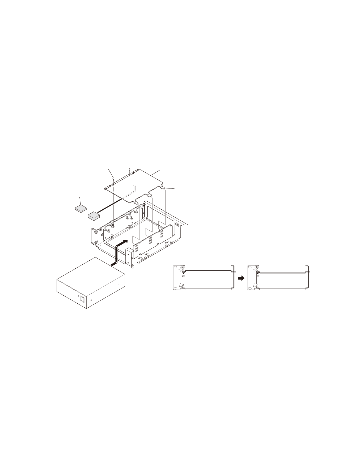
2. Accessory Cabinet
You can install optional accessories, such as a DC power
supply or duplexers, in the accessory cabinet.
1. Place the optional accessory in the cabinet as shown below.
2. If necessary, attach cushions (G13-1801-04 and/or G131802-04) to the top plate (J21-8559-04) in order to adjust
the space between the cabinet and the top plate. Then,
insert the 3 tabs of the plate into the slots in the side of
the cabinet. High, middle, or low positions are available.
To affi x the plate, inset and tighten the 2 screws on the
other side of the plate.
You can also fl ip the top plate upside-down to adjust the
height of the cabinet space.
Tighten screws
拧紧螺丝
Cushions / 缓冲垫
(G13-1801-04 or G13-1802-04)
(G13-1801-04或G13-1802-04)
or/或
Top plate / 顶板
(J21-8559-04)
安装
2. 附件柜
可以在附件柜中安装 DC 电源或双工器等选购附件。
1. 如下图所示,将选购附件安置在附件柜中。
2. 如有必要,可将缓冲垫 (G13-1801-04和/或G13-1802-
04) 安装到顶板 (J21-8559-04) 上,以调整附件柜和顶板
之间的空间。然后,将顶板的 3 个卡舌插入附件柜侧的插槽。
具有高、中、低三种位置。要固定顶板,请在顶板的另一
侧插入并拧紧 2 颗螺丝。
也可以翻转顶板,以调整附件柜空间的高度。
Insert the plate tabs to set the height
position (high, middle, or low).
插入顶板卡舌以设定高度(高、中或低)。
The top plate can be inverted to adjust the height of the cabinet space.
可以翻转顶板来调整附件柜空间的高度。
Fig. 2 /
图2
11
NXR-810
INSTALLATION /
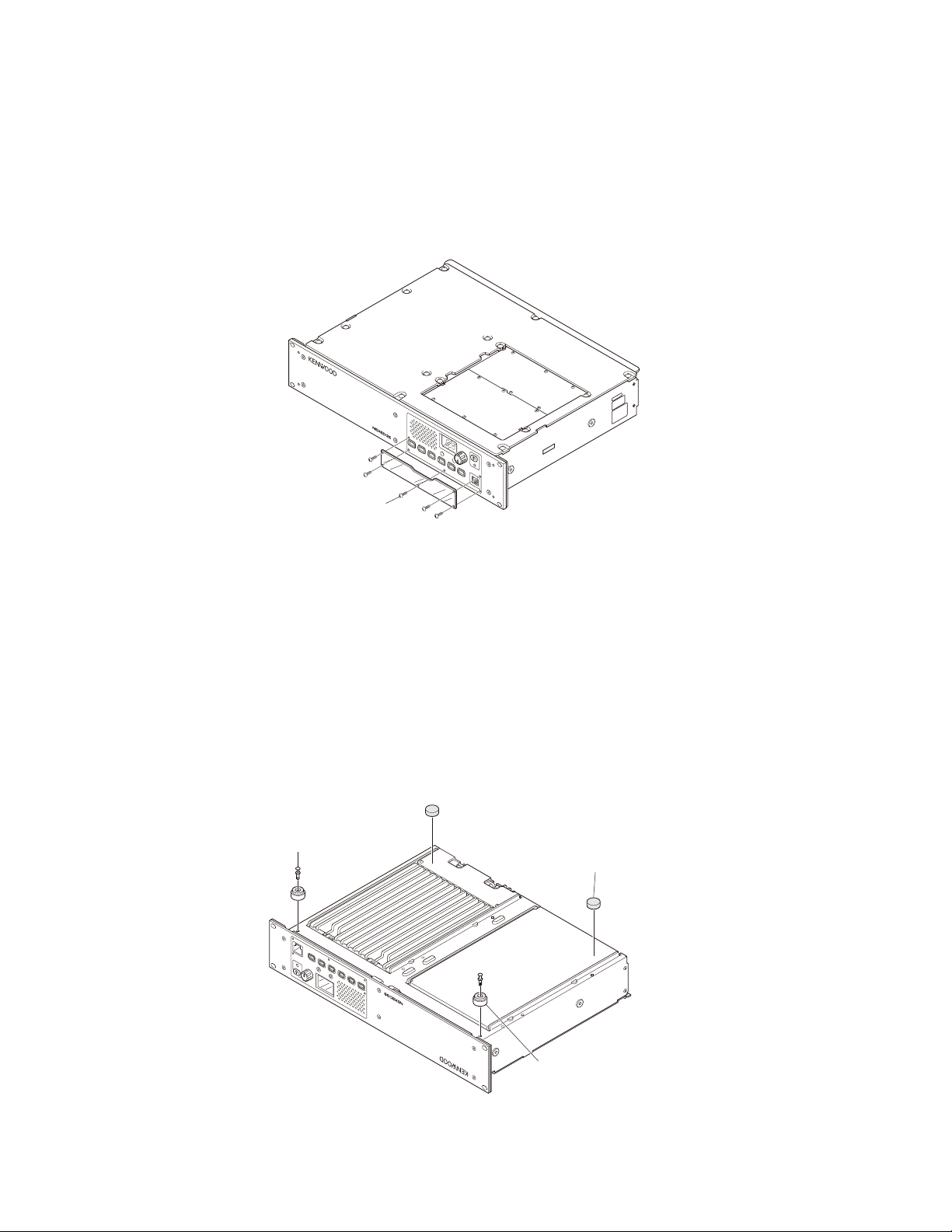
3. Key Cover
To avoid accidentally pressing the keys, you can install
the key cover.
1. Install and fix the key protector using the 5 supplied
screws (N35-3006-43).
Screws / 螺丝
(N35-3006-43) x 5
安装
3. 按键盖板
为避免不慎按下按键,可安装按键盖板。
1. 用附带的 5 颗螺丝 ( N35-3006-43) 安装并固定按键保护装
置。
Fig. 3 /
4. Desktop Repeater
When you use the repeater on a desktop, attach the 4
spacers to the base of the repeater as shown in the fi gure.
With these spacers attached, the front panel will not touch
the desk surface.
Pegs
Firmly press these pegs (J59-0302-05)
through the spacers to affix them to
the repeater.
拴钉
用力按这些拴钉(J59-0302-05),
使其穿过垫圈,把它们固定到中继台上。
图3
4. 桌面中继台
在桌面上使用中继台时,可以如图所示在中继台的底部安
装 4 个垫圈。安装这些垫圈之后,前面板就不会接触桌面。
Peel off the backing paper to attach
these spacers (J02-0492-04).
剥下衬纸来安装这些垫圈(J02-0492-04)。
12
Fig. 4 /
Spacers / 垫圈
(J02-0475-05)
图4
NXR-810
INSTALLATION /
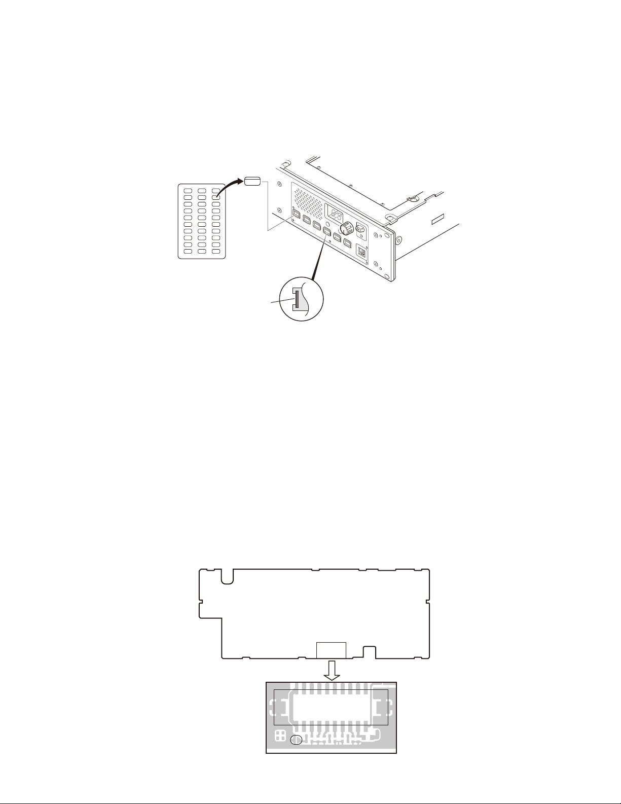
5. Installing Name Plates
Punch out the name plate card. Then insert the plates
onto the relative function keys.
You can reconfi gure the name plates at any time.
Punch out the
name plate cards
取出贴片
Squeeze and
insert the plates.
挤压并插入贴片。
Name plates for
the function keys
功能键的表示贴片
Name plates
贴片
Side view of the key
按键侧视图
安装
5. 安装按键功能表示贴片
取出按键功能表示贴片。然后将贴片插到相关的功能键上。
可随时重新装配按键功能表示贴片。
Fig. 5 /
MODIFICATION /
1. DC Source Switch
To prevent the power supply from turning off due to
misoperation of the DC source switch on the front panel or
accidents (tampering) after installation, the main unit can be
kept on regardless of the on/off setting of the DC source
switch on the front panel.
Using solder, short the PSW land near the CN40 connector.
Control unit / 控制单元
Component side / 元件面
图5
改装
1. DC 电源开关
为防止因前面板上的 D C 电源开关的误操作或安装后的意外
( 窜改 ) 而关闭电源,可以使主机不论前面板上的 D C 电源开
关的开 / 关设定如何,均保持在开启状态。
用焊料将 PSW 焊盘短接到 CN40 连接器附近。
PSW
CN40
13
NXR-810
MODIFICATION /
2. Single Antenna
The NXR-810 can be used as a base station by sharing an
external antenna connector for both transmitting and receiving data.
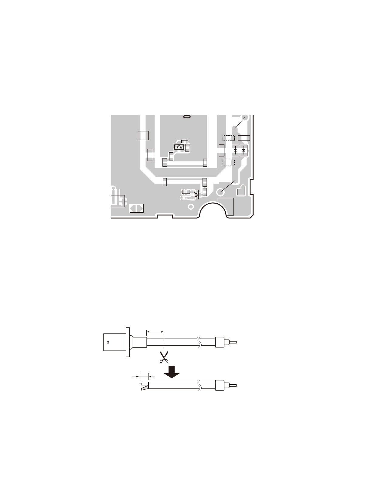
2-1. Modifi cation
1. Using a soldering iron, delete C76 and add C73 and C78
(100pF; C93-0572-05) on the Final unit (A/3).
Final unit (A/3) / 末级单元(A/3)
Component side / 元件面
ANT SW
CN204
改装
2. 单天线
使发射和接收信号共用一个外部天线连接器,可以将 NXR-
810 用作基站。
2-1. 更改
1. 在末级单元 (A/3) 上,用烙铁除去 C76 并增加 C73 和 C78
(100pF;C93-0572-05)。
C78
C76
C73
CN2
GND
RX
2. Short-circuit the printed pattern of ANT SW near the
CN204 connector by soldering.
3. Disconnect the pin connector from CN101 of the TX-RX
unit.
Remove the two screws used for securing the BNC con-
nector on the back panel of the unit. Detach the antenna
cable assy. (E30-3418-15)
4. Cut off the coaxial cable of the removed antenna cable
assy on the BNC connector side.
Strip off the insulation of the cut-off coaxial cable to pre-
pare it to be soldered.
About / 约
20mm
About / 约
8~10mm
Strip off the insulation so that
the cable can be soldered.
剥下绝缘材料以便焊接。
2. 以焊接方式将 ANT SW 的印刷图案短接到 CN204 连接器附近。
3. 从 TX-RX 单元的 CN101 断开针脚连接器。
拆下用于将 B N C 连接器固定在单元背板上的两颗螺丝。拆
下天线电缆组件。(E30-3418-15)
4. 切断已拆下的天线电缆组件的 BNC 连接器侧的同轴电缆。
剥下所切同轴电缆的绝缘材料,做好焊接准备。
Cut off the coaxial cable at this point.
在此处切断同轴电缆。
14
NXR-810
MODIFICATION /
2-2. Connection
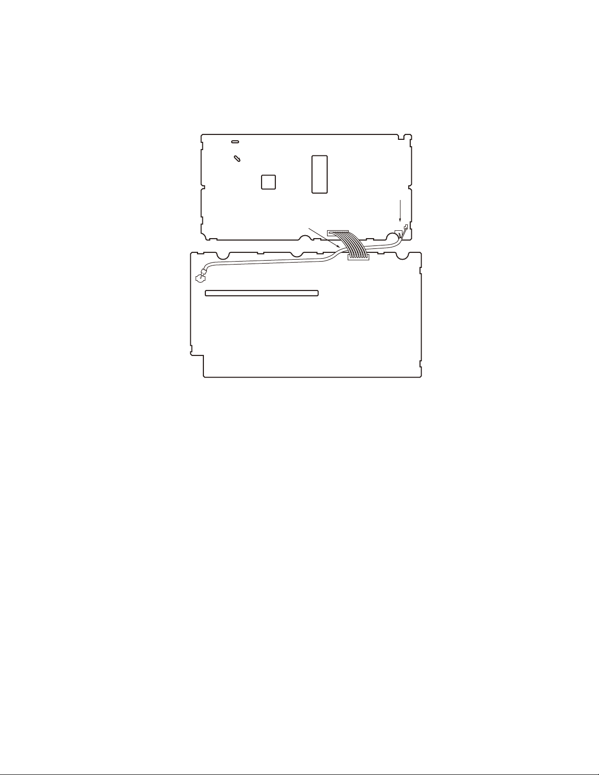
1. Solder the prepared coaxial cable to the Final unit (A/3).
2. Connect the pin connector of the coaxial cable to CN101
of the TX-RX unit.
Route the coaxial cable
under the lead wire extending from CN204 and CN801.
将同轴电缆布置在从CN204和
CN801伸出的导线下面。
Style the coaxial cable as illustrated in the figure.
CN101
使同轴电缆的样式如图中所示。
TX-RX unit / TX-RX单元
Component side / 元件面
改装
2-2. 连接
1. 将准备好的同轴电缆焊接到末级单元 (A/3)。
2. 将同轴电缆的针脚连接器连接到 TX-RX 单元的 CN101。
Final unit (A/3)
Component side
末级单元(A/3)
元件面
Solder the coaxial
cable.
焊接同轴电缆。
CN204
CN801
GND
RX
2-3. Setting the FPU
Set the channel to be used as “Simplex” using the FPU.
Check and readjust the transmit power if needed.
3-3. 设置 FPU
使用 FPU,将信道设置为用作“单工”。
如有必要,请检查或重新调整发射功率。
15
NXR-810
DISASSEMBLY FOR REPAIR /
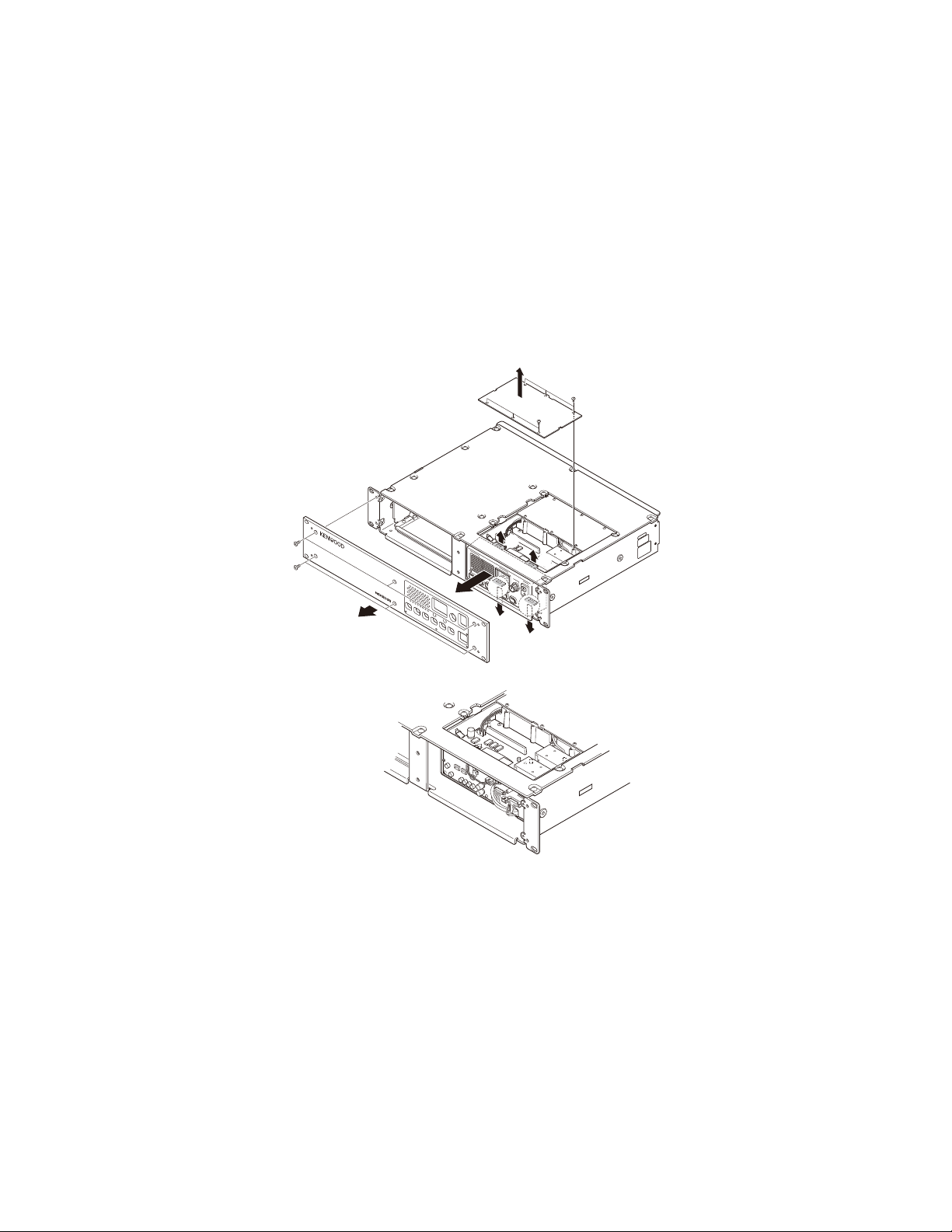
1. How to Remove the Panel Assy (ABS)
Note: You can remove the panel assembly (ABS) without
removing the top panel (A62-1148-03).
1. To remove the panel (TX-RX, w ), loosen the 6 screws ( q ).
2. To remove the panel assembly (Front, r ), loosen the 6
screws ( e ).
3. The panel assembly (ABS) is securely fastened by 4 tabs
( t ) on the top and bottom. You can remove the panel assembly by pulling to the front while you are pulling up the
tabs.
维修拆卸
1. 如何拆下面板组件 (ABS)
注意 :
您可以拆下面板组件(ABS) 而不拆下顶板 (A62-1148-
03)。
1. 要拆下面板 (TX-RX, ② ),请松开 6 颗螺丝(①)。
2. 要拆下面板组件(前部,④ ),请松开 6 颗螺丝(③)。
3. 面板组件 (ABS)由上下4个卡舌(⑤)牢牢固定。在向上
拔卡舌的同时向前拉面板组件,便可将其拆下。
@
:
:
.
.
;
=
=
=
=
16

NXR-810
CIRCUIT DESCRIPTION /
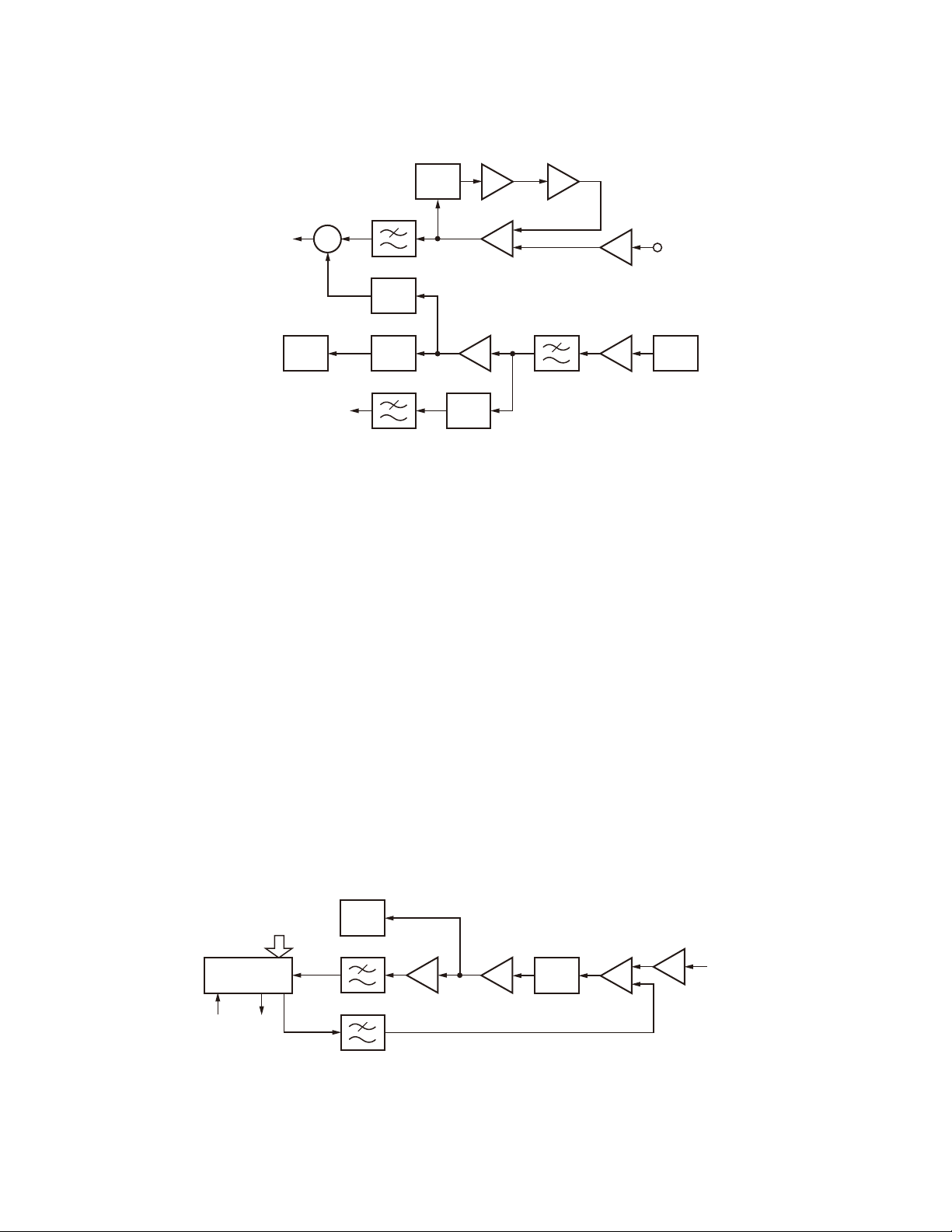
1. Outline
The NXR-810 is a UHF repeater operating in the 400~
470MHz frequency range.
2. TX-RX unit
TX-RX unit (X57-795) consists of the following circuit.
(1) Internal/external reference circuit
(2) Transmitter reference 16.8MHz PLL circuit
(3) Transmitter main PLL circuit
(4) Modulation level adjustment circuit
(5) Front-end circuit
(6) 1st-Mixer circuit
(7) IF circuit
(8) Receiver PLL circuits
(9) AVR circuits
(10) Other circuits
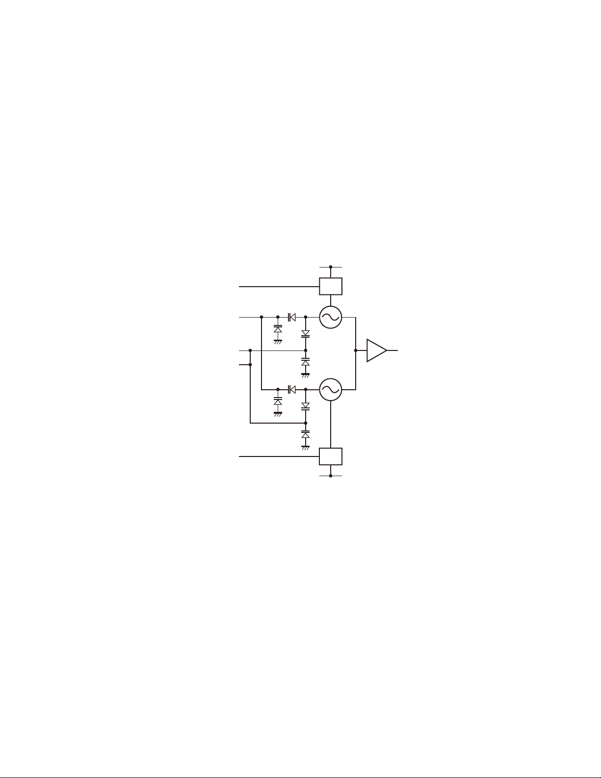
2-1. Internal/External reference circuit
The internal reference circuit consists of X500, Q502,
Q504 and D505. The output of 19.2MHz VCTCXO (X500) is
fed to buffer amplifi er Q502. The higher harmonic wave is
attenuated by the LPF. This reference signal is fed to IF IC
(IC304) as the 2nd Local signal through the Tripler.
The internal reference signal is amplified by Q504 to
achieve the needed level for PLL ICs. That signal is divided
by a Wilkinson divider. The divided signal is fed to the PLL
IC for the receiver. Another signal is fed to the transmitter
reference 16.8MHz PLL IC through PIN diode switch (D505)
which switches the Internal or external reference.
The external reference circuit consists of CN500, Q501,
Q503, IC500, IC501, D503 and D504. The external reference signal (10MHz/0dBm) input from CN500 is fed to buffer amplifi er Q501 and is amplifi ed by Q503. Q503 is a dual
gate MOS-FET. The output of amplifi er (Q503) is detected
by D503 and that DC voltage is amplified by IC500 (B/2).
The amplifi ed DC voltage is compared to the reference voltage by IC500 (A/2). The difference of voltages is amplifi ed
by IC500 (A/2) and is fed to the gate-2 terminal of Q503. The
voltage of the Q503 gate-2 terminal is controlled automatically to constantly maintain the power output of amplifier
(Q503). The output of amplifi er (Q503) is fed to the transmitter reference 16.8MHz PLL IC through the PIN diode switch
(D504) which switches the Internal or External reference.
The PIN diode switches (D504, D505) are controlled by
the I/O expander IC (IC805 Pin15). The I/O expander IC is
controlled by the MCU which is in the Control unit (X53-449).
If internal reference is selected by FPU, the I/O expander IC
outputs an “H” status. This signal sets power switch Q506
to ON. Then D505 is activated.
If external reference is selected, the I/O expander IC outputs an “L” status. This signal sets power switch Q500 to
ON. Then D504 is activated.
电路说明
1. 概述
NXR-810 是在 400 ~ 470MHz 频率范围内工作的 VHF 中继台。
2. TX-RX 单元
TX-RX 单元 (X57-795) 由以下电路组成。
(1) 内部 / 外部基准电路
(2) 发射机基准 16.8MHz PLL 电路
(3) 发射机主 PLL 电路
(4) 调制电平调整电路
(5) 前端电路
(6) 第 1 混频器电路
(7) IF 电路
(8) 接收机 PLL 电路
(9) AVR 电路
(10) 其他电路
2-1. 内部 / 外部基准电路
内部基准电路由 X500、Q502、Q504 和 D505 组成。19.2MHz
VCTCXO(X500) 的输出被送入缓冲放大器 Q502。较高的谐波由
LPF 衰减。该基准信号作为第 2 本地信号通过三倍频器送到
IF IC(IC304)。
内部基准信号由 Q504 放大,以获得 PLL IC 的所需电平。
该信号由 Wilkinson 分配器进行分割。分割的信号被送入接
收机的 PLL I C。另一信号通过可进行内部基准或外部基准信
号切换的 PIN 二极管开关 (D505) 送入 16.8MHz PLL IC。
外部基准电路由 CN500、Q501、Q503、IC500、IC501、D503
和 D504 组成。从 C N500 输入的外部基准信号 (10MHz/0dBm)
被送到缓冲放大器 Q501, 由 Q503 放大。Q503 为双栅 MOSFET。放大器 (Q503) 的输出由 D503 进行检测,DC电压由
IC500( B/2) 放大。放大的 DC 电压由 I C500(A/2) 与基准电压
进行比较。电压差由 IC500( A /2) 放大,并被送入 Q503 的栅
2 端子。Q503 栅 -2 端子的电压为自动控制,以稳定地保持放
大器 ( Q503) 的功率输出。放大器 (Q503) 的输出通过可进行
内部基准或外部基准信号切换的 PIN 二极管开关 ( D504) 送入
16.8MHz PLL IC。
PI N 二极管开关 (D504, D505) 由 I/ O 扩展器 IC(IC805 针
脚 15) 控制。I / O 扩展器 I C 由控制单元 ( X53-449) 内的 M C U
控制。
如果 FPU 选择了内部基准,则 I/O 扩展器 IC 输出“H”状态。
该信号开启 Q506 电源开关。然后 D505 被激活。
如果选择了外部基准,则 I/O 扩展器 IC 输出“L”状态。
该信号开启 Q500 电源开关。然后 D504 被激活。
17
NXR-810
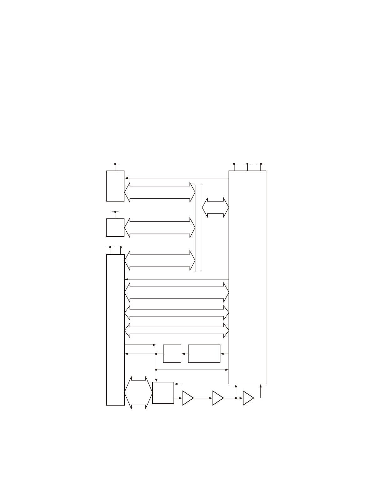
CIRCUIT DESCRIPTION /
D503
Detector
REF
LPF
3dB
ATT
3dB
ATT
10MHz or
19.2MHz
X58-5090-10
D504,D505
SW
RX VCO
/PLL
2nd Lo
Fig. 1 Internal/external reference circuit /
AMP
IC500(B/2)
AGC AMP
Q503
AMP
Q504
X3
Q202LPF
电路说明
AMP
IC500(A/2)
EXT_IN
10MHz
Buffer
Q501
LPF
图 1 内部 / 外部基准电路
AMP
Q502
CN500
X500
OSC
19.2MHz
2-2. Transmitter reference 16.8MHz PLL circuit
The transmitter reference 16.8MHz PLL circuit produces
the reference frequency signal for the Transmitter Main PLL
circuit and modulates the low-frequency components.
The circuit consists of IC600, IC601, IC602, IC603, IC604,
Q601, Q602, Q603, and X600.
The VCXO (X600) signal enters the buffer amplifi er Q603
and is amplifi ed by Q602. The higher harmonic wave is attenuated by the LPF and returns to IC602. Its phase is compared with that of the reference frequency 5kHz.
The phase difference signal produced by the comparing
phase is converted to a DC voltage by a lag-lead type loop
fi lter. This DC voltage is input to the IC604 invert amplifi er
and is synthesized with the modulating signal. This DC voltage is input to the X600 control voltage terminal for controlling the VCXO oscillating frequency 16.8MHz.
The 16.8MHz oscillating signal is fed to the Q603 buffer
amplifi er. The output signal of the buffer amplifi er is used as
the reference frequency signal of the transmitter main PLL
circuit.
SPSCLK0
/16_8PCS
IC602
MOD
PLL IC
Ref
LDT
10MHz
or 19.2MHz
SPSD0
X58-5100-10
TX VCO
/PLL
LPF
Loop filter
16.8MHz
AMP
Q602
2-2. 发射机基准 16.8MHz PLL 电路
发射机基准 16.8MH z PLL 电路产生发射机主 P LL 电路的基
准频率信号,并调制低频分量。
该电路由IC600、IC601、I C602、IC603、I C604、Q601、
Q602、Q603 和 X600 组成。
VCXO(X600) 信号进入缓冲放大器 Q603,由 Q602 放大。较
高的谐波由 LPF 衰减并返回 IC602。其相位与基准频率 5kHz
的相位进行对比。
通过相位对比产生的相位差信号由一个滞后超前式环路滤
波器转换为 DC 电压。该 D C 电压被输入 IC604 反相放大器并
与调制信号合成。该 DC 电压被输入用于控制 VCXO振荡频率
16.8MHz. 的 X600 控制电压端子。
16.8M H z 震荡信号被送入 Q603 缓冲放大器。缓冲放大器的
输出信号用作发射机主 PLL 电路的基准频率信号。
Buffer
Q603
X600
OSC
16.8MHz
AMP
IC604
AMP
IC603
MB
18
Fig. 2 Transmitter reference 16.8MHz PLL circuit /
图 2 发射机基准 16.8MHz PLL 电路
NXR-810
CIRCUIT DESCRIPTION /
2-3. Transmitter Main PLL circuit (SUB unit)
VCO
■
The TX VCO circuit consists of two VCOs (VCO A X58510: Q352, VCO B X58-510: Q353). Those VCOs generates
a transmit carrier. VCO A Q352 produces a transmitter frequency from 400.000MHz to 434.995MHz. VCO B Q353
produces a transmitter frequency from 435.000MHz to
470.000MHz.
Those VCO oscillation frequencies are determined by two
systems of voltage control terminals: “CV” and “TXASSIST”.
The voltage control terminals, “CV” and “TXASSIST”, are
controlled by the PLL IC (X58-510: IC300) and MCU (X53449: IC20) and the output frequency changes continuously
according to the applied voltage. For the modulation input
terminal, “MO”, the output frequency changes according to
the applied voltage.
TXVCOA
TX_CV
MO
TXASSIST
D355
D352
D357
电路说明
2-3. 发射机主 PLL 电路 (SUB 单元 )
■ VCO
TX VCO 电路由两个 VCO(VCO A X58-510:Q352,VCO B X58510:Q353) 组成。这些 VCO 生成发射载波。VCO A Q352 产生
从 400.000MHz 到 434.995MHz 的发射机频率。VCO B Q353 产
生从 435.000MHz 到 470.000MHz 的发射机频率。
这些 VC O 振荡频率由电压控制端子的两个系统 :“CV”和
“TXASSIST”决定。
电压控制端子“CV”和“TXASSIST”由 PLL IC(X58510:I C300) 和 MCU(X53-449:IC20) 控制,并根据施加的电压
连续输出频率变化。对于调制输入端子“MO”,输出频率根据
施加的电压改变。
80C
SW Q350
Buffer
D358D359
VCO_A
Q352
VCO_B
Q353
Q354
VO
D353
TXVCOB
Fig. 3 Transmitter VCO circuit /
PLL IC (X58-510: IC300)
■
The PLL IC compares the differences in phases of the
VCO oscillation frequency and the transmitter PLL reference
signal (16.8MHz), returns the difference to the VCO CV terminal and realizes the “Phase Locked Loop” for the return
control. This allows the VCO oscillation frequency to accurately match (lock) the desired frequency.
When the frequency is controlled by the PLL, the frequency convergence time increases as the frequency difference increases when the set frequency is changed. To
supplement this, the MCU is used before control by the
PLL IC to bring the VCO oscillation frequency close to the
desired frequency. As a result, the VCO CV voltage does not
change and is always stable at approx. 3.0V.
D360D361
SW Q351
80C
图 3 发射机 VCO 电路
■ PLL IC(X58-510: IC300)
PLL IC 对比 VCO 振荡频率和发射机 PLL 基准信号 (16.8MHz)
的相位差,将相位差返回 VCO CV 端子,实现返回控制的“锁
相环路”。这可以使 VC O 震荡频率与所需的频率精确匹配 ( 锁
定)。
频率由 PLL 控制时,频率锁定时间将随着设定频率改变时
频率差的增大而增加。为对此进行补充,在由 PLL IC 控制之
前使用 MC U 以使 VCO 振荡频率接近所需的频率。因此,VC O
CV 的电压不变,始终稳定在约 3.0V。
19
NXR-810
CIRCUIT DESCRIPTION /
The desired frequency is set for the PLL IC by the MCU
(X53-449: IC20) through the 3-line “SPSD0”, “SPSCLK0”,
“/TXPCS” serial bus. Whether the PLL IC is locked or not is
monitored by the MCU through the “LDT” signal line. If the
VCO is not the desired frequency (unlock), the “LDT” logic
is low.
SPSCLK0
Buffer
Q300
FIN
Fig. 4 Transmitter Main PLL circuit /
2-4. Modulation level adjustment circuit
The Modulation level adjustment circuit adjusts the modulation waveform balance. This circuit consists of IC804,
IC603, IC604, IC605 and IC606.
The modulating signal comes from the Control unit (X53-
449) through the interface connector (CN800 Pin 14). The
modulating signal is produced by the modulation lowpitched tone to the transmitter modulation 16.8MHz PLL circuit and adds the high-pitched modulation to the transmitter
main PLL.
IC804 is an electronic volume control IC. It has 8 electronic volume control circuits. The modulation level adjustment circuit uses 2 electronic volume control circuits in
IC804. The 1st electronic volume control circuit adjusts the
modulating signal and is fed to IC603 and the 2nd electronic
volume control circuit. The 2nd electronic volume control
circuit adjusts the modulating signal and is fed to IC606.
IC603 is an inverting amplifier for inverting the amplification of the modulating signal. The output of IC603 and
the charge pump output of IC602 (Transmitter modulation
16.8MHz PLL IC) are synthesized by IC604 and is fed to
VCXO (X600).
IC606 is a non-inverting amplifi er. The output of the 2nd
electronic volume control circuit is amplifi ed by IC606 and is
fed to the transmitter main PLL circuit.
/TXPCS
BPF
电路说明
PLL IC的所需频率由 MCU(X53-449: I C20) 通 过 3 线 路
“SPSD0”、“SPSCLK0”、“/TXPCS”串行总线进行设定。PLL IC
锁定与否由 MCU 通过“LDT”信号线路进行监测。如果 VCO 不
是所需的频率 ( 失锁 ),则“LDT”逻辑较低。
SPSD0
TX VCO/PLL
Ref 16.8MHz
LDT
Loop filter
IC300
LPF
TX_CV
图 4 发射机主 PLL 电路
2-4. 调制电平调整电路
调制电平调整电路用于调整调制波形平衡。该电路由
IC804、IC603、IC604、IC605 和 IC606 组成。
调制信号通过接口连接器 (CN800 针脚 14) 来自控制单元
(X53-449)。调制信号由到发射机调制 16.8MHz PLL 电路的调
制低调音产生,并把高调调制加到发射机主 PLL。
I C804 是一个电子音量控制 IC。它有 8 个电子音量控制电
路。调制电平调整电路使用 IC804 中的 2 个电子音量控制电路。
第 1 电子音量控制电路调制调制信号,并送入 IC603 和第 2
电子音量控制电路。第 2 电子音量控制电路调整调制信号并
送入 IC606。
I C603 是一个反相放大器,用于变换调制信号的放大。
IC603 的输出和 IC602( 发射机调制 16.8MHz PLL IC) 的电荷
泵输出由 IC604 合成并送入 VCXO(X600)。
I C606 是一个非反相放大器。第 2 电子音量控制电路的输
出由 IC606 放大并送入发射机主 PLL 电路。
20
X58-5100-10
TX VCO
/PLL
X600
OSC
16.8MHz
AMP
IC606
AMP
IC604
AMP
IC603
VREF
IC605
MO
EVOL
IC804
MB
Fig. 5 Modulation level adjustment circuit /
CN800
MOD
图 5 调制电平调整电路
NXR-810
CIRCUIT DESCRIPTION /
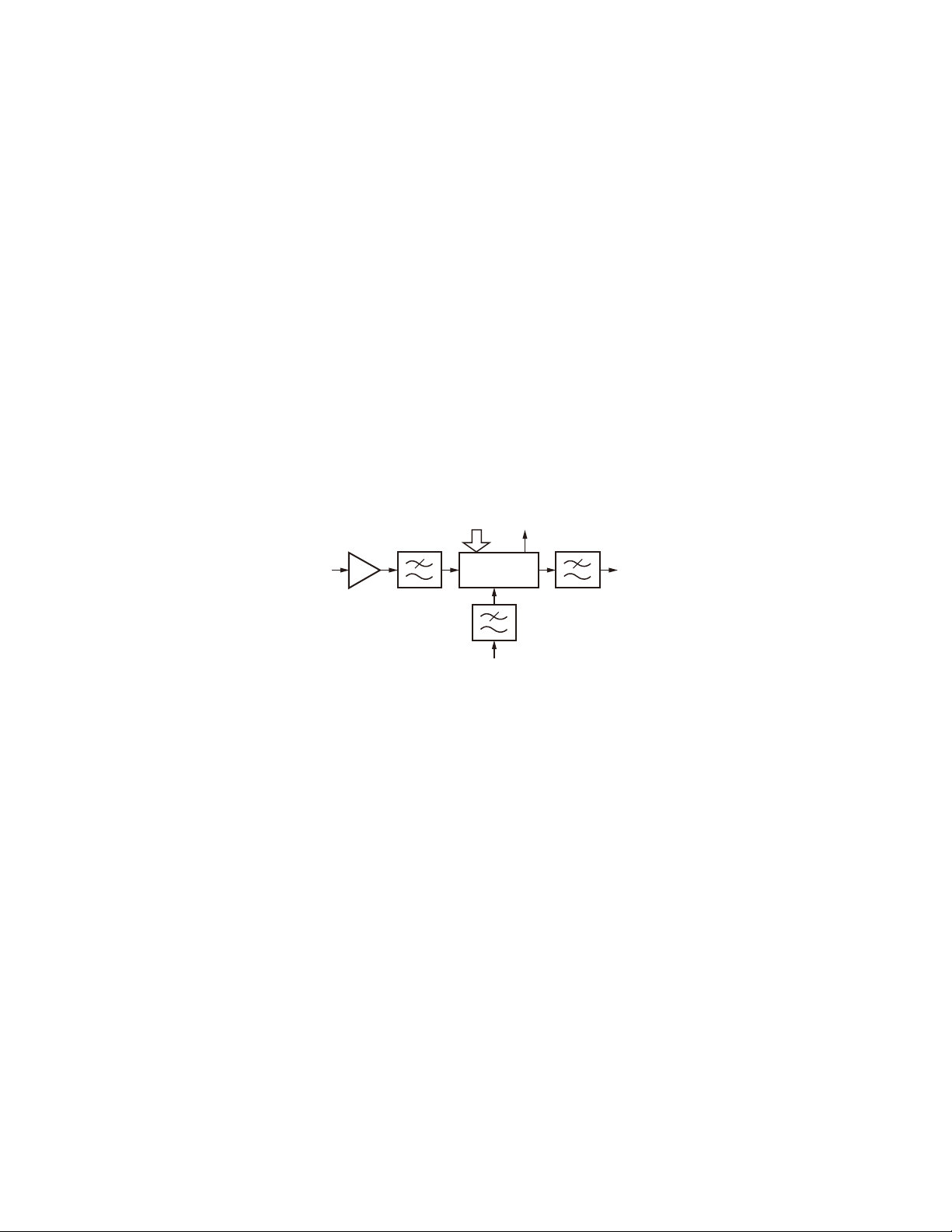
2-5. Front-end circuit
The front-end circuit consists of former LPF, former BPF
(D105, D106, D107 and D108), RF Low Noise Amplifier
(Q101), latter BPF (D100, D101, D103 and D104), and latter
LPF. The BPF covers frequency ranges 400 to 470MHz.
The former LPF, former BPF, latter BPF, and latter LPF attenuate the unwanted signals and send only the necessary
signal to the fi rst mixer.
LNA AMP
BPF
Q101
400~
470MHz
EVOL
IC804
Fig. 6 Front-end circuit /
Buffer
IC100
电路说明
2-5. 前端电路
前端电路由前级LPF、前级 BPF(D105、D106、D107 和
D108)、R F 低噪音放大器 (Q101)、 后级 BPF(D100、D101、
D103 和 D104)、以及后级 LPF 组成。BPF 覆盖的频率范围为
400 到 470MHz。
前级 LPF、前级 BPF、后级 BPF 和后级 LPF 衰减不需要的信
号,然后仅将必要的信号发送给第一混频器。
BPF LPFHPFLPF
Buffer
IC101
图 6 前端电路
RX ANT
CN101
400~
470MHz
2-6. 1st-Mixer circuit
The filtered signal from the front-end circuit is heterodyned with the first local oscillator signal from the PLL
frequency synthesizer circuit at the first mixer (IC300) to
become a 58.05MHz fi rst intermediate frequency (IF) signal.
400~470MHz
341.95~411.95MHz
Fig. 7 1st-Mixer circuit /
2-7. IF circuit
The fi rst IF signal is amplifi ed by the IF Post Amp (Q301)
and passed through a four-pole monolithic crystal filter
(XF300) to reject adjacent channel signals. The fi ltered fi rst
IF signal is amplified by the IF AGC amplifier (Q300) and
then applied to the IF system IC (IC403). The IF system IC
provides a second mixer, AGC amplifi er, and RSSI (Received
Signal Strength Indicator).
The second mixer mixes the fi rst IF signal with the 57.6
MHz of the second local oscillator output and produces the
second IF signal of 450kHz.
The second IF signal is passed through the ceramic fi lter
(CF401, CF402 and CF403) to reject the adjacent channel
signal. The fi ltered second IF signal is amplifi ed by the second IF amplifi er (IC404) and AGC amplifi er (IC403).
The signal from the AGC amplifi er is input to the AD converter (X53-449: IC20) through the ceramic fi lter (CF400) and
operational amplifi er (IC400 and X53-449: IC20).
2-6. 第 1 混频器电路
来自前端电路的过滤信号与第一混频器 (IC300) 的 P L L 频
率合成器电路的第一本地振荡信号进行外差,成为 58.05MHz
的第一中频 (IF) 信号。
Mixer
IC300
IF1
58.05MHz
1st Local
图 7 第 1 混频器电路
2-7. 中频电路
第一中频信号由 IF 放大器 ( Q301) 放大,并经过一个四极
的单片晶体滤波器 (XF300) 以消除临近信道的信号。滤波后
的第一中频信号由 I F A G C 放大器 ( Q300) 放大后,加到中频
系统IC(IC403) 上。中频系统 IC 提供一个第二混频器、AGC
放大器和 RSSI( 接收信号强度指示器 )。
第二混频器混合第一中频信号及 57.6MHz 的第二本地振荡
器输出,生成 450kHz 的第二中频信号。
第二中频信号通过陶瓷滤波器 (CF401、CF402 和 CF403) 以
消除临近信道的信号。经过滤波的第二种频信号由第二 IF 放
大器 (IC404) 和 AGC 放大器 (IC403) 放大。
AGC 放大器的信号通过陶瓷滤波器 ( C F400) 和运算放大器
(IC400 和 X53-449:IC20) 输入 AD 转换器 (X53-449:IC20)。
21

NXR-810
IF AGC AMP
Q300
RSSI
450kHz
CN802
AGC
CIRCUIT DESCRIPTION /
MCF
IF POST AMP
Diff AMP
IC401(B/2)
AMP
IC409(A/2,B/2)
IF AMP
IC400
Buffer
IC402
Buffer
IC401(A/2)
IC405
SW
XF300
IC406
SW
Q301
RSSI
CF400
CF402
CF403
CF401
电路说明
58.05MHz
IF IC
IF2
IC408SWIC407
SW
IC403
IF AMP
IC404
IF1
2nd Lo
57.6MHz
AGC
Fig. 8 IF circuit /
2-8. Receiver PLL circuit (SUB unit)
VCO
■
RX VCO circuit consists of two VCOs (VCO A X58509: Q352, VCO B X58-509: Q353). Those VCOs generate a 1st local signal. For the VCO oscillation frequency,
the 1st local signal is 341.95 to 411.95MHz. (VCO A:
341.95~376.95MHz, VCO B: 376.95~411.95MHz)
Those VCO oscillation frequency is determined by two
systems of voltage control terminals “CV” and “RXASSIST”.
The voltage control terminals, “CV” and “RXASSIST”,
are controlled by the PLL IC (X58-509: IC300) and the MCU
(X53-449: IC20) and the output frequency changes continuously according to the applied voltage.
RXVCOA/B
RX_CV
RXASSIST
D355
D352
D357
图 8 中频电路
2-8. 接收机 PLL 电路 (SUB 单元 )
■ VCO
RX VCO 电路由两个 VCO(VCO A X58-509:Q352,VCO B X58509:Q353) 组成。这些 VCO 生成第 1 本地信号。对于 VCO 振荡
频率,第 1 本地信号为 341.95 到 411.95MHz。(VCO A:341.95
~ 376.95MHz,VCO B:376.95 ~ 411.95MHz)
这些 VC O 振荡频率由电压控制端子的两个系统 :“CV”和
“RXASSIST”决定。
电压控制端子“CV”和“RXASSIST”由 PLL IC(X58509:I C300) 和 MCU(X53-449:IC20) 控制,并根据施加的电压
连续输出频率变化。
80C
Q350
SW
Q351
Buffer
D358D359
VCO_A
Q352
VCO_B
Q353
Q354
VO
22
D353
D360D361
Fig. 9 Receiver VCO circuit /
图 9 接收机 VCO 电路
NXR-810
CIRCUIT DESCRIPTION /
PLL IC (X58-509: IC300)
■
PLL IC compares the differences in phases of the VCO
oscillation frequency and the VCTCXO reference frequency,
returns the difference to the VCO CV terminal and realizes
the “Phase Locked Loop” for the return control. This allows
the VCO oscillation frequency to accurately match (lock) the
desired frequency.
When the frequency is controlled by the PLL, the frequency convergence time increases as the frequency difference increases when the set frequency is changed. To
supplement this, the MCU is used before control by the
PLL IC to bring the VCO oscillation frequency close to the
desired frequency. As a result, the VCO CV voltage does not
change and is always stable at approx. 3.0V.
The desired frequency is set for the PLL IC by the MCU
(X53-449: IC20) through the 3-line “SPSD0”, “SPSCLK0”,
“/RXPCS_TR” serial bus. Whether the PLL IC is locked or
not is monitored by the MCU through the “LDR” signal line.
If the VCO is not the desired frequency (unlock), the “LDR”
logic is low.
SPSCLK0
Buffer
Q300
FIN
/RXPCS
LPF
电路说明
■ PLL IC(X58-509: IC300)
PLL IC 对比 VCO 震荡频率和 VCTCXO 基准频率的相位差,将
相位差返回 VCO CV 端子,实现返回控制的“锁相环路”。这
可以使 VCO 震荡频率与所需的频率精确匹配 ( 锁定 )。
频率由 PLL 控制时,频率锁定时间将随着设定频率改变时
频率差的增大而增加。为对此进行补充,在由 PLL IC 控制之
前使用 MC U 以使 VCO 震荡频率接近所需的频率。因此,VC O
CV 的电压不变,始终稳定在约 3.0V。
PLL IC的所需频率由 MCU(X53-449: I C20) 通 过 3 线 路
“SPSD0”、“SPSCLK0”、“/RXPCS_TR”串行总线进行设定。PLL
IC 锁定与否由 MCU 通过“LDR”信号线路进行监测。如果 VCO
不是所需的频率 ( 失锁 ),则“LDR”逻辑较低。
SPSD0
RX VCO/PLL
IC300
LDT
Loop filter
RX_CV
Fig. 10 Receiver PLL circuit /
2-9. AVR circuit
The 13.6V Power Source (+B) is provided through the
Connector (CN701) from the Final unit (X45-393). +B is connected to a FET switch (Q702, Q703) and CN700. Q702
and Q703 are controlled by the “SBC” signal from the MCU
which is in the Control unit (X53-449). If “SBC” logic is
high, Q702 and Q703 turn on. The 13.6V power source (SB)
which is turned on by Q702 and Q703 is provided to the 8V
AVR IC (IC702) and CN700. CN700 is connected to the Control unit (X53-449) to provide the +B power source and the
SB power source.
IC702 supplies 8V to the VCO, 15V DC/DC converter IC
(IC701), AVR IC (IC700) and FET switches (Q700, Q701).
IC701 is a step-up switching regulator. IC701 regulates 8V
to 15V and supplies the 15V power source to the “assist circuit” and “front-end BPF tuning circuit”. The FET switches
(Q700, Q701) are controlled by the I/O expander IC (IC805).
When Q700 and Q701 turn on, the 8V power source is provided to receiver section.
LPF
Ref 19.2MHz
图 10 接收机 PLL 电路
2-9. AVR 电路
13.6V 电源 (+B) 通过连接器 (CN701) 从末级单元 (X45-
393) 提供。+B 连接到 FE T 开关 (Q702,Q703) 和 CN700。Q702
和 Q703 由控制单元 (X53-449) 内来自 M C U 的“S B C”信号控
制。如果“SBC”逻辑高,则 Q702 和 Q703 开启。由 Q702 和
Q703 开启的 13.6V 电源 (SB) 被提供到 8V AVR IC(IC702) 和
C N700。C N700 连接到控制单元 (X53-449) 以提供 + B 电源和
SB 电源。
I C702 将 8V 提供到 V C O、15V DC/DC 转换器 IC(IC701)、
AVR IC(IC700) 和 FET 开关 (Q700、Q701)。IC701 是一个升压
型开关稳压器。IC701 将 8V 调节到 15V,向“辅助电路”和“前
端 BPF 调谐电路”提供 15V 电源。FET 开关 ( Q700、Q701) 由
I/O 扩展器 IC(IC805) 控制。当 Q700 和 Q701 开启时,8V 电
源提供到接收机部分。
23
NXR-810
CIRCUIT DESCRIPTION /
IC700 regulates 5V to 8V. The output of IC700 is provided
to the FET switches (Q705, Q706) and AVR IC (IC703). The
FET switches (Q705, Q706) are controlled by the I/O expander IC (IC805). When Q705 and Q706 turn on, the 5V
power source is provided to the receiver section, IF section
and IC704. IC704 regulates 5V to 3V. The 3V power source
is provided to the Mixer IC (IC300). IC703 regulates 5V to
3.3V. The output of IC703 is provided to the IF section.
+B
from Final unit
(X45-393 A/3)
+B,SB
to Control unit
(X53-449)
CN701
CN700
Q702,Q703
SW
SBC
SB
IC702
8V AVR
电路说明
I C700 将 5V 调 节 到 8V。I C700 的输出被提供到 FET 开关
(Q705、Q706) 和 AVR IC(IC703)。FET 开关 (Q705、Q706) 由
I/O 扩展器 IC(IC805) 控制。当 Q705 和 Q706 开启时,5V 电
源提供到接收机部分、IF 部分和 IC704。IC704 将 5V 调节到
3V。3V 电源提供到混频器IC(IC300)。IC703 将 5V 调节到 3.3V。
IC703 的输出被提供到 IF 部分。
80C
IC701
Q700,Q701
SW
5V AVR
IC700
RXC
Q705,Q706
SW
RXC
3.3V AVR
IC703
Ripple Filter
Ripple Filter
Ripple Filter15V DC/DC
Ripple Filter
IC704
3V AVR
80C_1
80C_2
150C_1
150C_2
80R
50C
50R
30R
33C
Fig. 11 AVR circuit /
2-10. Other circuit
EEPROM
■
The EEPROM (IC802) has a data capacity of 2Kbit. It
stores the tuning data in frequency adjustment.
Temperature sensor
■
The temperature sensor (IC800) monitors temperature
around the VCTCXO (X500).
I/O expander
■
The I/O expander IC (IC805) controls the power sources,
fan, analogue switches, and the transmit power control circuit. IC805 is controlled by the MCU which is in the Control
unit (X53-449).
Electronic volume control IC
■
The Electronic volume control IC (IC804) adjusts the
modulating signal, center frequency of the front-end BPF,
and the power of the RF fi nal amplifi er. IC804 is controlled
by the MCU which is in the Control unit.
图 11 AVR 电路
2-10. 其他电路
■ EEPROM
EEPROM(IC802) 具有 2Kbit 数据容量。它存储频率调整中
的调谐数据。
■温度传感器
温度传感器 (IC800) 监测 VCTCXO(X500) 周围的温度。
■ I/O 扩展器
I/O 扩展器 IC(IC805) 控制电源、风扇、模拟开关以及发
射功率控制电路。IC805 由控制单元 (X53-449) 内的 MCU 控制。
■电子音量控制 IC
电子音量控制 IC(IC804) 调整调制信号、前端 BPF 的中心
频率以及 RF 末级放大器的功率。IC804 由控制单元内的 M C U
控制。
24
NXR-810
CIRCUIT DESCRIPTION /
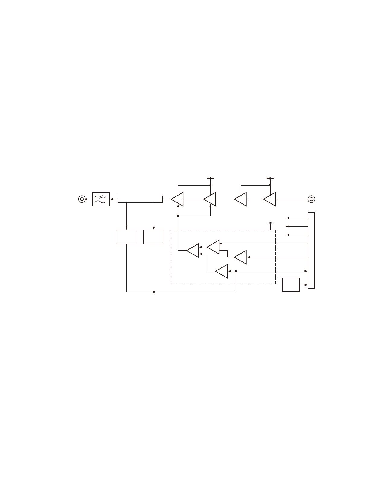
3. Final unit
The RF fi nal amplifi er unit (X45-393) amplifi es the trans-
mitter power to a specifi ed level.
This unit consists of the following circuits:
(1) Driver and Final power amplifi er circuit
(2) CM coupler circuit
(3) Filter circuit
(4) APC circuit
(5) High temperature detector circuit
(6) FAN action control circuit
(7) AVR circuit
3-1. Driver and Final power amplifi er circuit
The transmit signal from the TX IN terminal CN1 of the
Final unit (X45-393) is amplifi ed by Q1, Q2 and Q3, and is
passed to the final stage Q4. The signal amplified by the
fi nal stage Q4 passes through the CM coupler circuit and
fi lter circuit, and is then fed to the antenna.
LPF
TX ANT
CM coupler
REV DET
D4
FW DET
D3
电路说明
3. 末级单元
RF 末级放大器单元 (X45-393) 将发射机功率放大到指定电
平。
该单元由以下电路组成 :
(1) 驱动及末级功率放大器电路
(2) CM 耦合电路
(3) 滤波电路
(4) APC 电路
(5) 高温检测器电路
(6) FAN 动作控制电路
(7) AVR 电路
3-1. 驱动及末级功率放大器电路
来自末级单元 (X45-393) 的 TX IN 端子 CN1 的发射信号由
Q1、Q2 和 Q3 放大,并传递到末级 Q4。由末级 Q4 放大的信号
通过 CM 耦合电路和滤波电路,然后被送到天线。
+B
Final AMP
Q4
Vcont
Auto power control
Drive AMP
Q3
Drive AMP
Q2
Limiter AMP
IC201(B/2)
80T
Drive AMP
Q1
80T
CN801
8TC
FAN
ASWC
PLIM
CN1
DC AMP
IC202(A/2)
REV DET
FW DET
Fig. 12 Driver and Final power amplifi er circuit /
3-2. CM coupler circuit
The CM coupler circuit is a line for detecting forward
wave and refl ected wave. Forward wave is detected by D1,
and is converted into DC voltage. If an abnormal antenna
load is connected, reflected wave is detected by D3 and
converted into DC voltage.
3-3. Filter circuit
This circuit removes harmonics from the transmitter output and sends fi ltered signals to the antenna.
3-4. APC circuit
The automatic transmission power control (APC) circuit
stabilizers the transmitter output power at a pre-determined
level. DC voltage from the CM coupler circuit is amplifi ed by
the DC amplifi er IC202 (1/2). IC202 (2/2) compares the APC
control voltage (RAMP) generated by the MCU (X53-449)
and the DC amplifi er IC201 (1/2, 2/2) with the output voltage
from IC202 (1/2) to control the gate voltage for amplifi er Q3
and fi nal amplifi er Q4.
RAMP
PRE AMP
IC201(A/2)
Buffer AMP
IC202(B/2)
FDT
Temp1
TH201
图 12 驱动及末级功率放大器电路
3-2. CM 耦合电路
CM 是一条用于检测前向波和反射波的线路。前向波由 D1
检测,并转换为 DC 电压。如果连接了异常天线负载,反射波
由 D3 检测并转换为 DC 电压。
3-3. 滤波电路
该电路从发射机输出中消除谐波,并将滤波的信号发送到
天线。
3-4. APC 电路
自动发射功率控制(APC) 电路将发射机输出功率稳
定在预定的电平。CM耦合电路的DC电压由 DC放大器
IC202(1/2) 放大。IC202(2/2) 将 MCU(X53-449) 和 DC 放大器
IC201(1/2,2/2) 产生的 AP C 控制电压 (RAMP) 与IC202(1/2)
的输出电压进行比较,以控制放大器 Q3 和末级放大器 Q4 的
栅电压。
25
NXR-810
CIRCUIT DESCRIPTION /
3-5. High temperature detector circuit
To prevent thermal destruction of amplifi er Q3 and fi nal
amplifier Q4, this circuit reduces the APC control voltage
(RAMP) when the temperature of amplifi er Q3 and fi nal amplifi er Q4 rises. The MCU detects the temperature with the
thermistor (TH201) and controls the APC voltage (RAMP).
3-6. FAN action control circuit
The FAN action control circuit consists of the FAN and
switching transistor Q207. It is controlled by the MCU (X53-
449). If the FAN action is set to “Temperature”, the cooling
fan is turned ON or OFF according to temperature. If the
FAN action is set to “Continuous”, the cooling fan operates
continuously, but Q207 stays ON.
3-7. AVR circuit
The 13.6V power source (+B) is provided through connector CN201 to the Final unit (X45-393 A/3). +B is connected
to CN203 to supply the 13.6V power source for the TX-RX
unit (X57-795). +B is a power source for the “final amplifi er”, “drive amplifi er” and fan. IC203 regulates the +B voltage to 8V. This 8V power source is connected to the FET
switches Q203, Q204, Q205, and Q206. Q204 and Q206
are controlled by the “8TC” signal from the I/O expander IC
which is in the TX-RX unit (X57-795). If “8TC” logic is high,
Q204 and Q206 turn on and supply the 8V power source
to the APC circuit and pre drive amplifi ers. Q203 and Q205
are controlled by the “ASWC” signal from the I/O expander
IC which is in the TX-RX unit (X57-795). If “ASWC” logic
is high, Q203 and Q205 turn on and supply the 8V power
source to the antenna switch circuit.
+B
from Final unit
(X45-393 B/3)
+B
to TX-RX unit
(X57-795)
CN201
CN203
电路说明
3-5. 高温检测器电路
为防止毁坏放大器 Q3 和末级放大器 Q4,该电路在放大器
Q3 和末级放大器 Q4 的温度升高时降低 APC 控制电压 (RAMP)。
MCU 用热敏电阻 (TH201) 检测温度并控制 APC 电压 (RAMP)。
3-6. FAN 动作控制电路
FA N 动作控制电路由 F AN 和开关晶体管 Q207 组成。它由
MCU(X53-449) 控制。如果把 FAN 动作设为“Temperature( 温
度)”,冷却风扇将根据温度开启或关闭。如果把 FAN 动作设
为“Continuous( 连续 )”,冷却风扇将连续运行,但 Q207 将
保持开启状态。
3-7. AVR 电路
13.6V 电源 (+B) 通过连接器 CN201 提供到末级单元 (X45-393
A/3)。+B 连接到 CN203,为 TX-RX 单元 (X57-795) 提供 13.6V
电源。+B 是“末级放大器”、“驱动放大器”和风扇的电源。
IC203 将 +B 电压调节到 8V。该 8V 电源连接到 FET 开关 Q203、
Q204、Q205 和 Q206。Q204 和 Q206 由 TX-RX 单元(X57-795)
内 I / O 扩展器 I C 的“8T C”信号控制。如果“8TC”逻辑高,
Q204 和 Q206 开启,并向 A PC 电路和预驱动放大器提供 8V 电
源。Q203 和 Q205 由 TX-RX 单元(X57-795) 内 I/O 扩展器 I C
的“ASWC”信号控制。如果“ASWC”逻辑高,Q203 和 Q205 开
启,并向天线开关电路提供 8V 电源。
Final AMP
Drive AMP
IC203
8V AVR
Q204,Q206
SW
8TC
Q203,Q205
SW
FAB
80T
80SW
Fig. 13 AVR circuit /
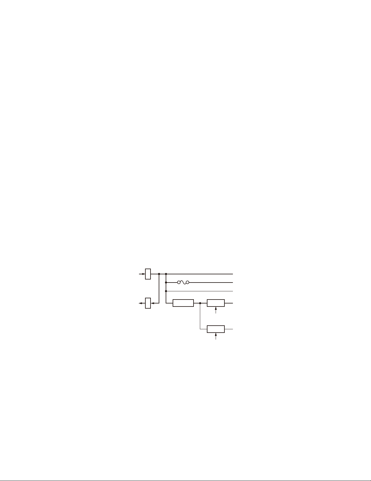
4. Control unit
The Control unit (X53-449) consists of the following cir-
cuits:
(1) MCU circuit
(2) Memory circuit
(3) DSP circuit
(4) Squelch circuit
(5) Power supply circuit
(6) Power supply voltage monitoring circuit
(7) 18.432MHz clock circuit
(8) Audio circuit
(9) Other circuit
26
ASWC
图 13 AVR 电路
4. 控制单元
控制单元 (X53-449) 由以下电路组成 :
(1) MCU 电路
(2) 存储电路
(3) DSP 电路
(4) 静噪电路
(5) 电源电路
(6) 电源电压监测电路
(7) 18.432MHz 时钟电路
(8) 音频电路
(9) 其他电路

NXR-810
CIRCUIT DESCRIPTION /
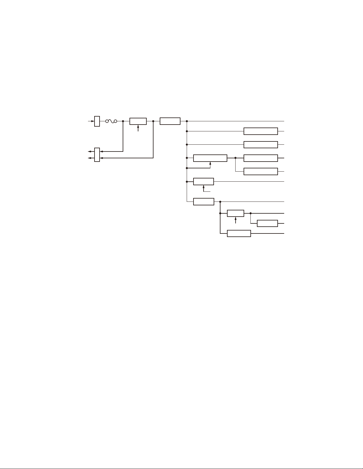
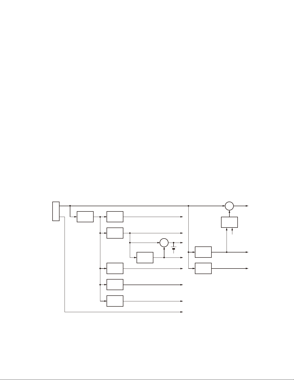
4-1. MCU circuit
The MCU (IC20) is a 32bit RISC processor, equipped with
a peripheral function and ADC/DAC.
This MCU operates at a 18.432MHz clock and 3.3V/1.5V
DC.
It controls the fl ash memory, SRAM, DSP, receive circuit,
transmitter circuit, and control circuit.
4-2. Memory circuit
The Memory circuit consists of the MCU (IC20), the
SRAM (IC9), and the fl ash memory (IC3).
The fl ash memory has a capacity of 32Mbit that contains
the transceiver control program for the MCU and stores the
data. It also stores the data for transceiver channels and
operating parameters that are written by the FPU. This program can be easily written from external devices.
The SRAM has a capacity of 1Mbit that contains work
area and data area.
Flash memory
■
Note: The fl ash memory stores the data that is written by
the FPU, tuning data (Deviation, Squelch, etc.), and firmware program.
电路说明
4-1. MCU 电路
MCU(IC20) 是一个 32 位 RISC 处理器,具备外围功能和
ADC/DAC。
该 MCU 以 18.432MHz 时钟和 3.3V/1.5V DC 运行。
它控制闪存、SRAM、DSP、接收电路、发射电路以及控制电路。
4-2. 存储电路
存储电路由 MCU(IC20)、SRAM(IC9) 和闪存 (IC3) 组成。
闪存具有 32Mbit 的容量,包含 MCU 的中继台控制程序并储
存数据。它也保存中继台信道的数据和由 FPU 写入的操作参数。
此程序很容易从外部设备写入。
SRAM 具有 1Mbit 的容量,包含工作区和数据区。
■闪存
注意 :
闪存存储 FPU 写入的数据、调谐数据 ( 频偏、静噪等 )
以及固件程序。
SRAM (static memory)
■
Note: The SRAM has a temporary data area and work area.
When the power supply is off, it is backed up by an internal
secondary lithium battery. Therefore, the saved data is not
lost.
4-3. DSP circuit
The DSP circuit consists of a DSP (IC6) and processes the
base band signal. The DSP operates on an external clock of
18.432MHz (the same as IC20). The I/O section operates at
3.3V and the core section operates at 1.6V. The DSP carries
out the following processes:
Digital processing
■
• 4Level FSK and Baseband fi lter processing
• Vocoder processing between audio codec and modulation/demodulation
• CAI processing, such as error correction encoding/decoding and interleaving
• AFC loop control
• Frame synchronization and Time tracking
• Data scrambling
Analog FM processing
■
• Pre-emphasis/De-emphasis
• QT/DQT encoding/decoding
• DTMF encoding/decoding
• Compressor/Expander processing
• Voice scrambler processing
■ SRAM( 静态存储器 )
注意 :
SRAM 含有临时数据区和工作区。当电源关闭时,则以
内部二次锂电池作为后备电源。因此,保存的数据不会丢失。
4-3. DSP 电路
DSP 电路由 DSP(IC6) 组成,可处理基带信号。DSP 在
18.432MHz 的外部时钟上运行 ( 与IC20 相同 )。I/O 部分以3.3V
运行,核心部分以 1.6V 运行。DSP 执行以下处理 :
■数字处理
• 4 级 FSK 和基带滤波处理
• 音频编解码器和调制 / 解调之间的声码器处理
• CAI 处理,例如纠错编码 / 解码和交错
• AFC 环路控制
• 帧同步和时间跟踪
• 数据扰频
■模拟 FM 处理
• 预加重 / 去加重
• QT/DQT 编码 / 解码
• DTMF 编码 / 解码
• 压缩器 / 扩展器处理
• 语音扰频器处理
Audio or Modulation function
■
• Transmit/Receive audio fi ltering processing
• Microphone amplifi er AGC processing
• Audio soft mute processing
• Modulation level processing
• Squelch Filtering
■音频或调制功能
• 发射 / 接收音频滤波处理
• 麦克风放大器 AGC 处理
• 音频软静音处理
• 调制电平处理
• 静噪滤波
27
NXR-810
CIRCUIT DESCRIPTION /
Other function
■
• Voting tone
• CWID
• Courtesy tone
• Repeater operating
• Analog/Digital Mixed mode
4-4. Squelch circuit
The Squelch circuit amplifi es the demodulated noise signal from IC6 after fi ltering through the BPF circuit. The processed digital noise signal is applied to CODEC IC14, and is
converted from digital to analog. The amplifi ed signal is then
converted to a DC signal by the detection circuit. The converted signal is fed back to IC20.
33M 33M 33A15M
/FRST
FLASH
IC3
33BU
A[0~21], D[0~15],
/RD, /WR, /CS0, /WP
电路说明
■其他功能
• 表决音
• CWID
• 礼貌音
• 中继台运行
• 模拟 / 数字混合模式
4-4. 静噪电路
通过 BPF 电路滤波后,静噪电路放大 IC6 的已解调噪音信号。
经过处理的数字噪音信号施加于 CODEC IC14,从数字转换为
模拟。随后,放大的信号由检测电路转换为 DC 信号。转换的
信号被反馈到 IC20。
/FRST
SRAM
IC9
33M 16M
DSP
IC6
A[0~17], D[0~7],
/RD, /WR, /CS2
A[0~20], D[0~15], /RD,
/WR, /HRDY, /CS3, /HDS2
/DRST
/MCCSXCN, /MCCSRCN, MCDICN,
MCDOCN, MCSCKCN
MCSCKAF, /MCCSAF, MCDIAF, MCDOAF
/SYMTIM, /DINT, /DWUP, FSDET, /HINT
/PCS_DSP
MAIN_CLK
/PDN,
LRCLK,
SDTI,
BICLK
Buffer
IC16
Squelch
DAC
IC14
VCTCXO
X1
(18.432MHz)
VREF
AMP
IC13(A/2,B/2)
AMP
Q4
MCU
IC20
/DRST
BSHIFT
XTAL_IN
LDR
ADC1
AMP
IC15(A/2)
28
Fig. 14 Control circuit /
图 14 控制电路
NXR-810
CIRCUIT DESCRIPTION /
4-5. Power supply circuit
The X53-449 circuit consists of IC301, IC302, IC303,
IC304, IC305 and IC306.
IC301 is a DC/DC converter that converts 13.6V to 6.0V.
This 13.6V voltage is supplied from TX-RX unit (X57-795).
IC302 is connected to IC301 and regulates the voltage
to 5.0V. IC303, IC304, IC305 and IC306 are connected to
IC301. IC303 and IC306 are 3.3V voltage regulators. IC304
is a 1.5V regulator IC, and IC305 is a 1.6V regulator IC.
CN302 is the connector for the lithium battery. The
lithium battery is used to back up the SRAM and RTC data
when no external DC power source is available.
4-6. Power supply voltage monitoring circuit
The X53-449 circuit consists of IC307, IC308, D303 and
Q301.
IC308 is a voltage detect IC and is used to generate the
“/RST” signal for the MCU (IC20).
This “/RST” signal is connected to the hardware reset pin
of MCU (IC20).
IC307 is a voltage detect IC and is used to generate the
“/BINT” signal for the MCU (IC20).
This “/BINT” signal is connected to the hardware interrupt pin of MCU (IC20). The software of the MCU (IC20)
runs to the sleep-mode to use the “/BINT” signal.
D303 and Q301 are used to generate the “OVRB” signal
for the MCU (IC20). The software of the MCU (IC20) runs to
the sleep-mode to use the “OVRB” signal.
电路说明
4-5. 电源电路
X53-449 电 路 由 I C301、I C302、I C303、I C304、IC305 和
IC306 组成。
I C301 是将 13.6V 转换为 6.0V 的 DC/DC 转换器。该13.6V
电压从 TX-RX 单元 (X57-795) 提供。
IC302 连接到 IC301 并将电压调节到 5.0V。IC303、IC304、
IC305 和 IC306 连接到 IC301。IC303 和 IC306 是 3.3V 稳压器。
IC304 是 1.5V 稳压器 IC,IC305 是 1.6V 稳压器 IC。
C N302 是锂电池的连接器。锂电池用于在无法使用外部 DC
电源时备份 SRAM 和 RTC 数据。
4-6. 电源电压监测电路
X53-449 电路由 IC307、IC308、D303 和 Q301 组成。
IC308 是电压检测 IC,用于产生 MCU(IC20) 的“/RST”信号。
该“/RST”信号连接到 MCU(IC20) 的硬件复位针脚。
IC307 是电压检测 IC,用于产生 MCU(IC20) 的“/BINT”信号。
该“/BINT”信号连接到 MCU(IC20) 的硬件中断针脚。
MCU(IC20) 的软件运行到休眠模式以使用“/BINT”信号。
D303 和 Q301 用于产生MCU(IC20) 的“OVRB” 信 号。
MCU(IC20) 的软件运行到休眠模式以使用“OVRB”信号。
CN301
B
SB
DC-DC
IC301
60DC
AVR
IC302
AVR
IC303
AVR
IC305
AVR
IC304
AVR
IC306
50M
33M
16M
15M
33A
RESET
IC308
Q303
SW
/RST
Fig. 15 Power supply circuit /
33BU
/OVRB
Q301
/BINT
IC307
图 15 电源电路
Q402
/OVRB
/BINT
SW
OR
Q401
AMP_SW
AMP_B
29
NXR-810
CIRCUIT DESCRIPTION /
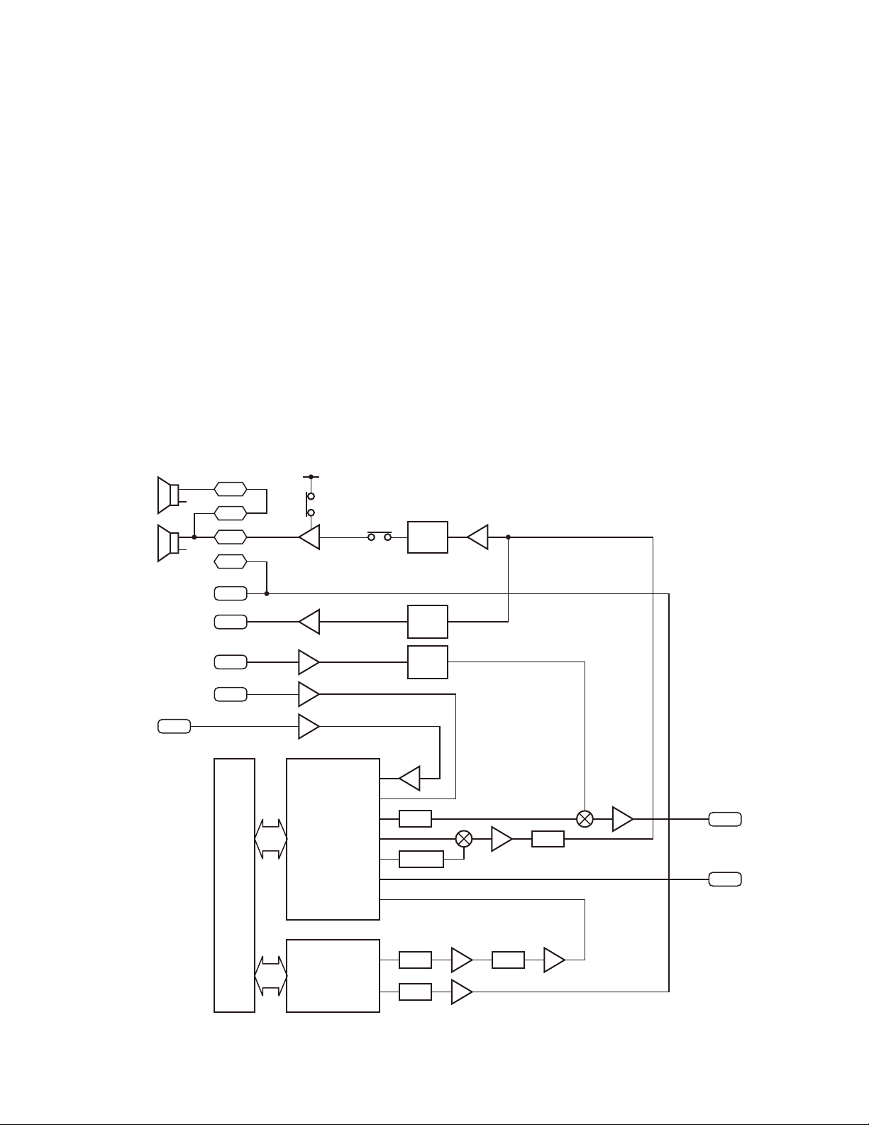
4-7. 18.432MHz clock circuit
The 18.432MHz clock is provided to the MCU (IC20),
DSP(IC6), and DAC (IC14) of the Squelch circuit.
4-8. Audio circuit
Audio amplifi er circuit
■
The audio amplifi er circuit is located in the control section
of the Control unit (X53-449). The 4W output audio power
is available from the pin 15 TEST/SPKR connector “SPO”,
“SPG” on the rear panel to the external speaker in the case
of a power supply voltage of 13.6V and a 4Ω load.
Microphone circuit
■
The signal from the microphone is passed through the
AGC circuit located in the Display unit (X54-373 A/2) so that
it may not saturate. This circuit consists of IC501, D501,
D502, Q501, and Q502. The AGC controls the amplifier
gains using the detected audio signal depending on the positive and negative peaks of the signal amplitude. The audio
signal goes to the control section of the Control unit (X53-
449) from the Display unit (X54-373 A/2).
AMP_B
AMP_SW
SW
IC402
INT_SP
EXT_SP
SPO
SPI
SPO
RD
Audio_AMP
电路说明
4-7. 18.432MHz 时钟电路
18.432MHz 时钟提供到 MCU(IC20)、DSP(IC6) 以及静噪电
路的 DAC(IC14)。
4-8. 音频电路
■音频放大器电路
音频放大器电路位于控制单元 (X53-449) 的控制部分。在
电源电压 13.6V、负载 4Ω 的情况下,从后面板上的针脚 15
TEST/SPKR 连接器“SPO,SPG”到外部扬声器可获得 4W 输出音
频功率。
■麦克风电路
麦克风的信号通过位于显示单元 (X54-373 A/2) 内的 A G C
电路,因此它不会饱和。该电路由 IC501、D501、D502、Q501
和 Q502 组成。A G C 利用检测的音频信号,根据信号振幅的正
负峰值控制放大器增益。音频信号从显示单元 (X54-373 A/2)
进入控制单元 (X53-449) 的控制部分。
DAC
IC412
MIC
RD
RA
TD
TA
DSP
IC6
IC501
MICADC0
MICADC1
MODDAC
MCU
IC20
SPDAC
PWM1
ADC1
Squelch DAC
IC14
IFR
IC412
IC412
IC405
(C/4)
LPF
CR-LPF
LPF
LPF
DAC
DAC
IC404(A/2)
DET
LPF
IC404
(B/2)
MOD
IF
signal
MOD
30
Fig. 16 Modulation circuit (Analog/Digital signal processing) /
图 16 解调电路 ( 模拟 / 数字信号处理 )
 Loading...