

Page 1
VHF DIGITAL BASE-REPEATER
NXR-710
SERVICE MANUAL
© 2009-12 PRINTED IN JA PAN
B51-8901-00 (N) 527
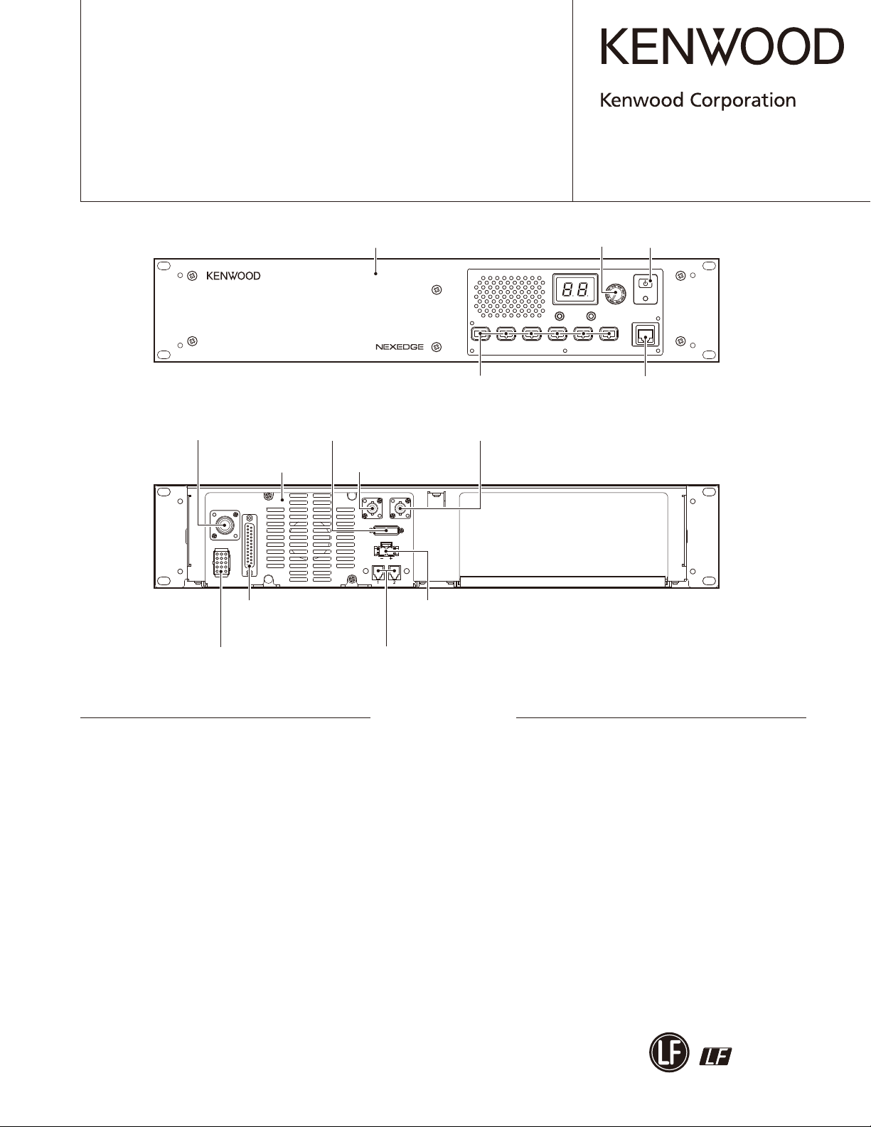
Antenna cable (TX OUT)
(E30-7528-15)
Rear panel
(A82-0077-02)
TX OUT
CONTROL
I/O
TEST/SPKR
Lead wire with connector
(DSUB25P)
(E37-1376-05)
Lead wire with connector
(ACC15P)
(E37-0913-05)
Front panel
(A62-1174-03)
Blade fuse (15A/32V)
(F05-1537-05)
Antenna cable (REF IN)
(E30-7690-05)
REF IN RX IN
FUSE
DC 13.6V
N SYNC
Modular jack x 2
(E58-0533-05)
Key top
(K29-9370-02)
Antenna cable (RX IN)
(E30-3418-15)
DC cord (Ext DC in)
(E30-3414-05)
Knob (Volume)
(K29-5389-03)
CH/STATUS
TX
VOLUME
BUSY
Knob (Power)
(K29-9106-04)
POWER
MIC
Modular jack
(E58-0522-05)
CONTENTS
GENERAL ................................................................... 2
SYSTEM SET-UP ....................................................... 3
REALIGNMENT ......................................................... 3
OPERATING FEATURES ........................................... 5
INSTALLATION .......................................................... 6
MODIFICATION ......................................................... 8
DISASSEMBLY FOR REPAIR .................................... 8
CIRCUIT DESCRIPTION ............................................ 9
COMPONENTS DESCRIPTION ............................... 18
PARTS LIST ............................................................. 20
EXPLODED VIEW .................................................... 36
PACKING .................................................................. 38
ADJUSTMENT ........................................................ 39
TERMINAL FUNCTION ........................................... 53
This product complies with the
directive for the European market.
RoHS
PC BOARD
FINAL UNIT (X45-3920-10) ................................. 58
CONTROL UNIT (X53-4490-10) .......................... 62
DISPLAY UNIT (X54-3580-20) ............................. 66
TX-RX UNIT (X57-7940-10) ................................. 70
RX VCO/PLL UNIT (X58-5070-10) ...................... 74
TX VCO/PLL UNIT (X58-5080-10) ...................... 75
INTERCONNECTION DIAGRAM ............................ 76
SCHEMATIC DIAGRAM .......................................... 78
BLOCK DIAGRAM ................................................... 96
OPTIONAL ACCESSORIES
KES-5 (EXTERNAL SPEAKER) ............................ 99
SPECIFICATIONS ................................. BACK COVER
This product uses Lead Free solder.
Page 2

NXR-710
Document Copyrights
Copyright 2009 by Kenwood Corporation. All rights re-
served.
No part of this manual may be reproduced, translated,
distributed, or transmitted in any form or by any means,
electronic, mechanical, photocopying, recording, or otherwise, for any purpose without the prior written permission
of Kenwood.
Disclaimer
While every precaution has been taken in the preparation
of this manual, Kenwood assumes no responsibility for errors or omissions. Neither is any liability assumed for damages resulting from the use of the information contained
herein. Kenwood reserves the right to make changes to any
products herein at any time for improvement purposes.
Firmware Copyrights
The title to and ownership of copyrights for firmware
embedded in Kenwood product memories are reserved for
Kenwood Corporation. Any modifying, reverse engineering, copy, reproducing or disclosing on an Internet website
of the firmware is strictly prohibited without prior written
consent of Kenwood Corporation. Furthermore, any reselling, assigning or transferring of the fi rmware is also strictly
prohibited without embedding the firmware in Kenwood
product memories.
Transceivers containing AMBE+2™ Vocoder:
The AMBE+2™ voice coding technology is embedded
in the fi rmware under the license of Digital Voice Systems,
Inc.
GENERAL
INTRODUCTION
SCOPE OF THIS MANUAL
This manual is intended for use by experienced technicians familiar with similar types of commercial grade communications equipment. It contains all required service
information for the equipment and is current as of the publication date. Changes which may occur after publication
are covered by either Service Bulletins or Manual Revisions.
These are issued as required.
ORDERING REPLACEMENT PARTS
When ordering replacement parts or equipment information, the full part identifi cation number should be included.
This applies to all parts: components, kits, or chassis. If the
part number is not known, include the chassis or kit number
of which it is a part, and a suffi cient description of the required component for proper identifi cation.
PERSONAL SAFETY
The following precautions are recommended for personal
safety:
• DO NOT transmit if someone is within two feet (0.6 meter) of the antenna.
• DO NOT transmit until all RF connectors are secure and
any open connectors are properly terminated.
• SHUT OFF this equipment when near electrical blasting
caps or while in an explosive atmosphere.
• All equipment should be properly grounded before powerup for safe operation.
• This equipment should be serviced by only qualified
technicians.
SERVICE
This transceiver is designed for easy servicing. Refer to
the schematic diagrams, printed circuit board views, and
alignment procedures contained within.
2
Page 3
Merchandise received
Choose the type of transceiver
NXR-710
SYSTEM SET-UP
Frequency range RF power Type
TX/RX 136~174MHz 50W K
1. Modes
User mode
PC mode
Repeater programming & setup
DC power supply or
duplexer?
NO
External speaker?
NO
Delivery
PC programming mode
PC test mode
PC tuning mode
See page 3.
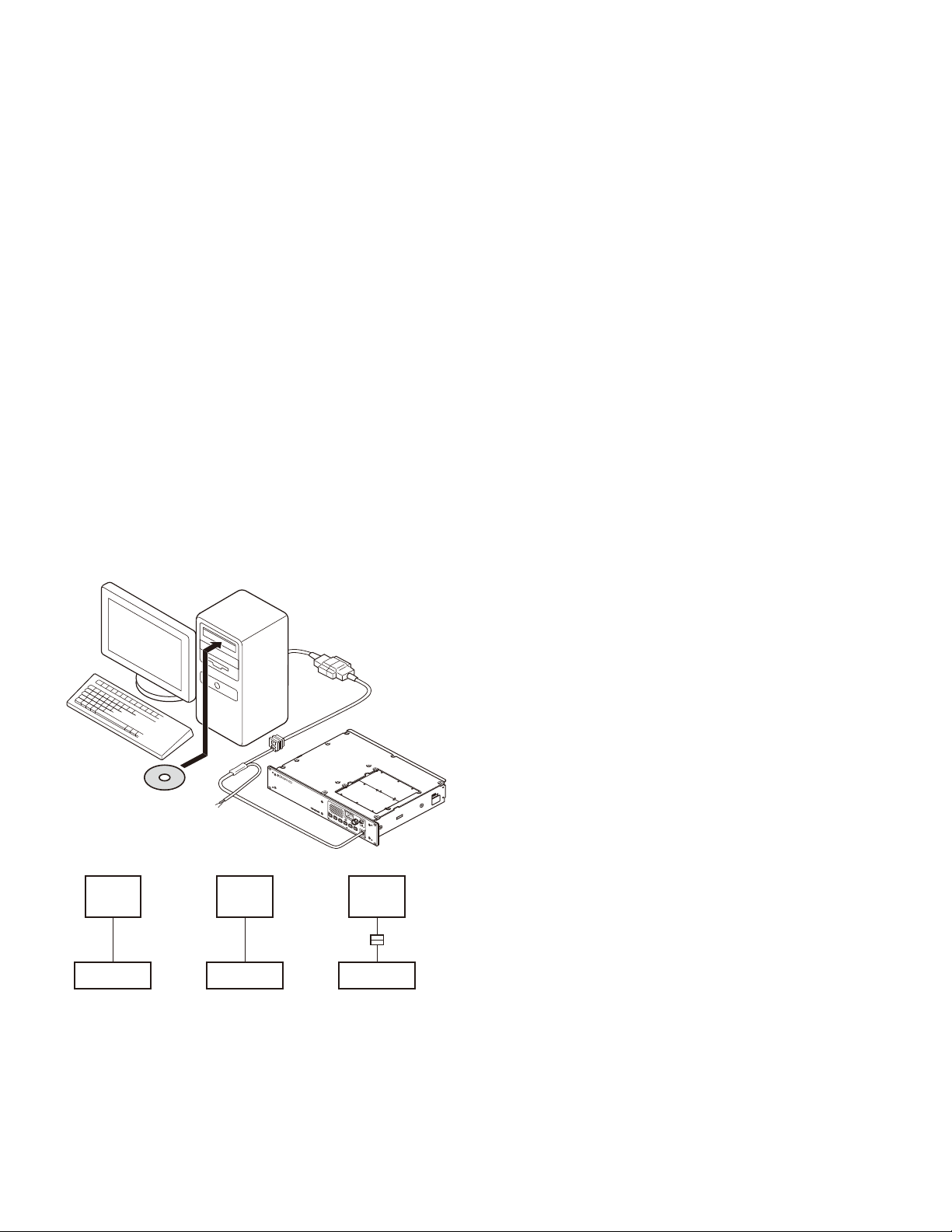
A personal computer, programming interface (KPG-46/46A), and
programming software (KPG-129D) are required for programming.
YES
YES
Installation in the optional space
(Option)
KES-5 installation
(Option)
See page 6.
See page 6.
REALIGNMENT
3. PC Mode
3-1. Preface
The NXR-710 is programmed by using a personal computer, programming interface (KPG-46/46A) and programming software (KPG-129D).
The programming software can be used with a PC. Figure 1 shows the setup of a PC for programming.
Firmware programming mode
Mode Function
User mode Use this mode for normal operation.
Use this mode to make various settings by
PC mode
PC programming
mode
PC test mode
Firmware programming mode
means of the FPU through the RS-232C
port.
Use to read and write frequency data and
other features to and from the repeater.
Use to check the repeater using the PC.
This feature is included in the FPU.
Use when changing the fi rmware program
of the fl ash memory.
2. How to Enter Each Mode
Mode Operation
User mode Power on.
PC mode Received commands from PC.
Firmware programming mode [PF1] + Power on (one second)
3-2. Connection Procedure
1. Connect the NXR-710 to the computer using the inter-
face cable and USB adapter (When the interface cable is
KPG-46A, the KCT-53U can be used.).
Note:
• You must install the KCT-53U driver in the computer to
use the USB adapter (KCT-53U).
• When using the USB adapter (KCT-53U) for the first time,
plug the KCT-53U into a USB port on the computer with
the computer power ON.
2. When power is applied, the user mode is entered im-
mediately. When the PC sends a command, the repeater
enters the PC mode and displays “PC” on the 7-seg-
ment LED. When data is being transmitted to the PC
from the repeater, the TX LED fl ashes. The BUSY LED
fl ashes when data from the PC is being received by the
repeater.
Note:
• The data stored in the personal computer must match
the model type, when it is written into the fl ash memory.
• Change the NXR-710 to PC mode, then attach the inter-
face cable.
3
Page 4
NXR-710
REALIGNMENT
3-3. KPG-46/KPG-46A Description
(PC programming interface cable: Option)
The KPG-46/46A is required to interface the NXR-710 to
the computer. It has a circuit in its D-sub connector (KPG46: 25-pin, KPG-46A: 9-pin) case that converts the RS-232C
logic level to the TTL level.
The KPG-46/46A connects the 8-pin microphone connector of the NXR-710 to the RS-232C serial port of the computer.
3-4. KCT-53U Description (USB adapter: Option)
The KCT-53U is a cable which connects the KPG-46A to
a USB port on a computer.
When using the KCT-53U, install the supplied CD-ROM
(with driver software) in the computer. The KCT-53U driver
runs under Windows 2000, XP or Vista (32-bit).
3-5. Programming Software KPG-129D Description
The KPG-129D is the programming software for the
transceiver supplied on a CD-ROM. This software runs under Windows XP, Vista or 7 on a PC.
The data can be input to or read from the NXR-710 and
edited on the screen. The programmed or edited data can
be printed out. It is also possible to tune the NXR-710.
PC
KPG-46 or KPG-46A or
KPG-46A + KCT-53U +
Tuning cable (E30-3383-05)
NXR-710
KPG-129D
4. Firmware Programming Mode
4-1. Preface
The NXR-710 uses fl ash memory to allow it to be easily
upgraded when new features are released in the future.
4-2. Connection Procedure
Connect the NXR-710 to the personal computer using
the interface cable (KPG-46/46A) and USB adapter (KCT-53U:
when the interface cable is KPG-46A, the KCT-53U can be
used.). (Connection is the same as in the PC Mode.)
Note:
You can only program firmware from the 8-pin microphone connector on the front panel. Using the 25-pin logic
interface on the rear panel will not work.
4-3. Programming
1. Start up the fi rmware programming software (Fpro.exe
(ver. 4.1 or later)). The Fpro.exe exists in the KPG-129D
installed folder.
2. Set the communications speed (normally, 115200 bps)
and communications port in the confi guration item.
3. Set the fi rmware to be updated by File name item.
4. Turn the NXR-710 power ON with the [PF1] key held
down. Then, “P.G.” is displayed.
5. Check the connection between the NXR-710 and the
personal computer, and make sure that the NXR-710 is in
the Program mode.
6. Press write button in the window. When the NXR-710
starts to receive data.
7. If writing ends successfully, the TX LED on the NXR-710
lights.
8. If you want to continue programming other NXR-710s,
repeat steps 4 to 7.
Note:
This mode cannot be entered if the Firmware Program-
ming mode is set to Disable in the Programming soft-
ware.
4
PC
D-SUB
(25-pin)
KPG-46
Transceiver
PC
D-SUB
(9-pin)
KPG-46A
Transceiver
Fig. 1
PC
USB
KCT-53U
KPG-46A
Transceiver
4-4. Function
If you press the [PF6] key while “P.G.” is displayed, the
display changes to “P G” to indicate that the write speed
is low speed (38400 bps). If you press the [PF6] key again
while “P G” is displayed, the display changes to “P G.” to
indicate that the write speed is mid speed (57600 bps). If
you press the [PF6] key again while “P G.” is displayed, the
display changes to “P.G.” to indicate that the write speed is
high speed (115200 bps).
Note:
Normally, write in the high-speed mode.
Page 5
OPERATING FEATURES
NXR-710
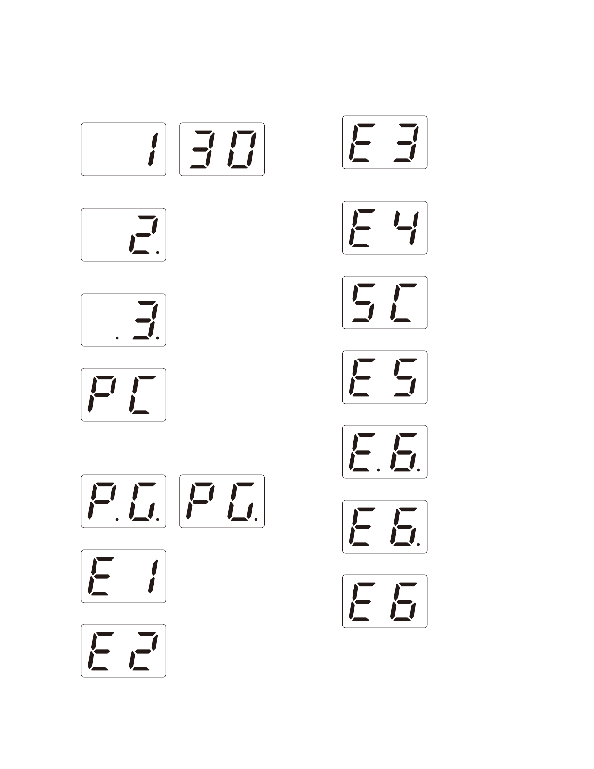
1. Two 7-segment LED Displays
• Channel display (1~30): While operating normally in user
mode.
• When the displayed channel is contained in scan sequence, the right side decimal point is displayed.
• When the displayed channel is the priority channel, the
left side decimal point is displayed.
• “PC” is displayed while in PC mode.
• “E3” is displayed when PLL is unlocked.
Receiver PLL unlocked = BUSY LED blinks.
Transmitter PLL unlocked = TX LED blinks.
• “E4” is displayed when PTT is attempted on a channel
number that has no TX frequency data programmed.
• “SC” is displayed while in scan mode.
• “E5” is ESN blank error.
• “PG” is displayed while in fi rmware programming mode.
2 decimal points displayed = 115,200 bps
1 decimal point displayed = 57,600 bps
No decimal = 38,400 bps
• “E1” is displayed when FPU data is not written.
• “E2” is displayed when the channel data is not written.
• “E.6.” is MCU internal RAM error.
• “E6.” is DSP RAM error.
• “E6” is MCU External RAM error.
5
Page 6
NXR-710
INSTALLATION
1. External Speaker (KES-5)
The NXR-710 has a built-in speaker (5W/8Ω), and the
external speaker output from the TEST/SPKR connector (15pin) on the rear of the radio is 4W/4Ω. Use external speaker
KES-5.
1-1. Connection for the KES-5 with the NXR-710
When taking the AF output from the TEST/SPKR
■
connector (15-pin) on the rear of the radio
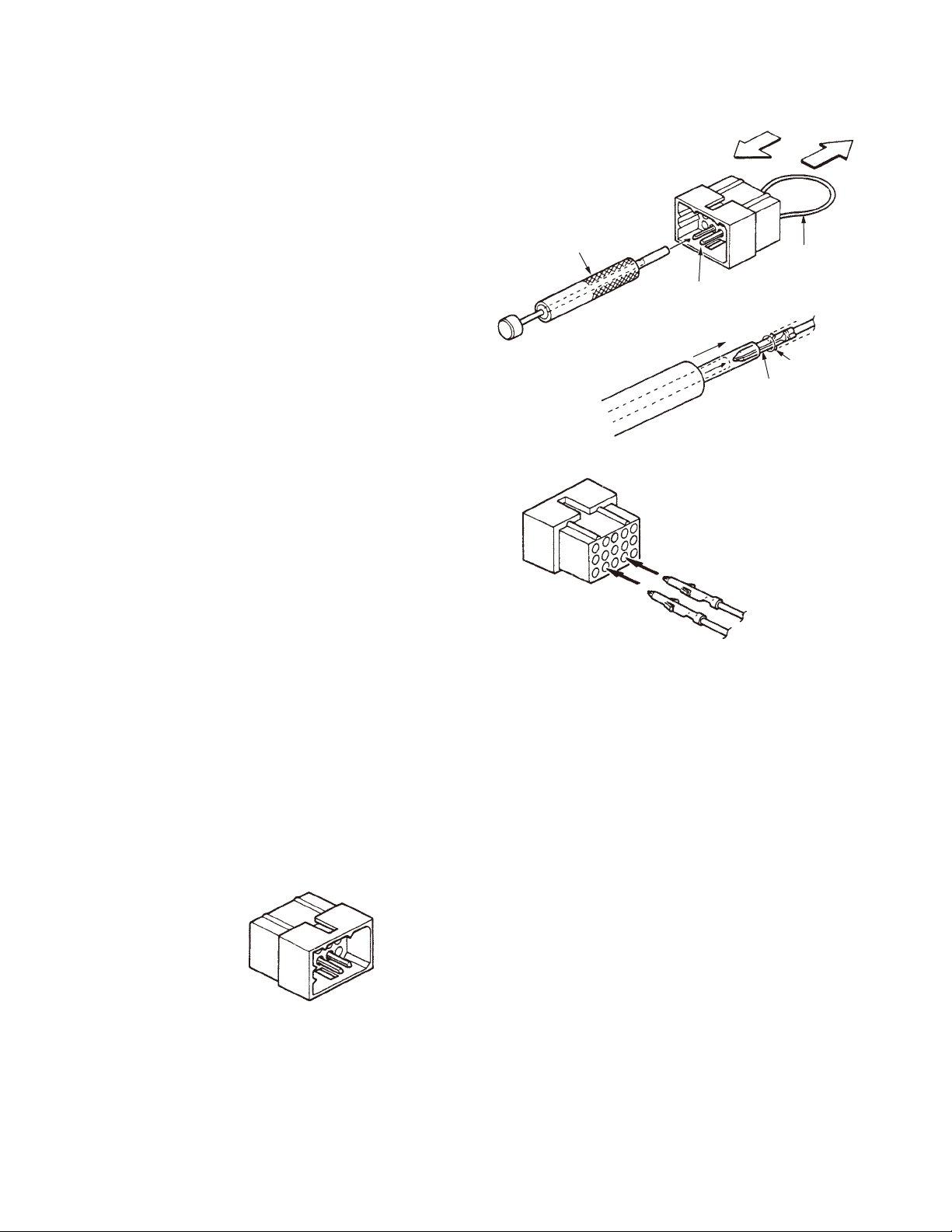
The following tools are required for changing the connector.
• Extracting tool
The following extracting tool is recommended:
Molex Inc. Order No.: J5800-002 (W05-0878-00)
1. Remove the connector with jumper from the external
speaker connector on the rear panel of the radio. (Fig.1-1)
Note: Save the jumper, which is required when the radio
is used without the external speaker.
2. Remove the terminals with the jumper from the connec-
tor housing holes number 9 and 12 using the extracting
tool.
Removing the jumper lead (Fig. 1-2)
1) Insert the extracting tool (J5800-002) into the connec-
tor while pushing the jumper lead in the direction of (a).
2) Push the extracting tool in to collapse the barbs of the
crimp terminal.
3) Pull out the lead while continuing to push the extract-
ing tool in the direction (b).
3. Reinsert the terminal with the black and white stripe lead
into hole number 12, and the terminal with the black lead
into hole number 6. (Fig. 1-3)
4. Attach the connector to the external speaker connector
on the radio.
Note:
Relationship between the TEST/SPKR connector (15-pin)
connection and speaker output:
• When pins 9 and 12 are shorted: The built-in speaker is
used.
• When pins 9 and 12 are open and output is from pins 6
and 12: KES-5 is used.
Square-type plug
(E31-3228-05)
Accessory
Fig. 1-1
(a)
(b)
Extracting tool
(11-03-0002)
Crimp termial
Jumper lead
Barbs
Crimp termial
Fig. 1-2
1
13
15
Crimp terminal
(E23-0613-05)
3
6
12
Black lead
Black/White lead
Fig. 1-3
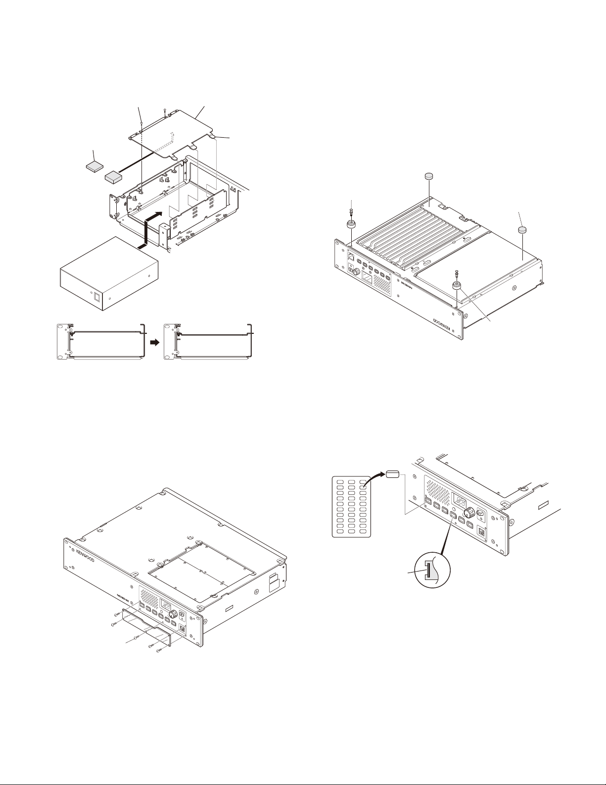
2. Accessory Cabinet
You can install optional accessories, such as a DC power
supply or duplexers, in the accessory cabinet.
1. Place the optional accessory in the cabinet as shown below.
2. If necessary, attach cushions (G13-1801-04 and/or G131802-04) to the top plate (J21-8559-04) in order to adjust
the space between the cabinet and the top plate. Then,
insert the 3 tabs of the plate into the slots in the side of
the cabinet. High, middle, or low positions are available.
To affi x the plate, inset and tighten the 2 screws on the
other side of the plate.
You can also fl ip the top plate upside-down to adjust the
height of the cabinet space.
6
Page 7
INSTALLATION
NXR-710
Top plate
Tighten screws
Cushion
(G13-1801-04 or
G13-1802-04)
or
The top plate can be inverted to adjust the height
of the cabinet space.
(J21-8559-04)
Insert the plate
tabs to set the
height position
(high, middle,
or low).
4. Desktop Repeater
When you use the repeater on a desktop, attach the 4
spacers to the base of the repeater as shown in the fi gure.
With these spacers attached, the front panel will not touch
the desk surface.
Pegs
Firmly press these pegs
(J59-0302-05) through the
spacers to affix them to
the repeater.
Fig. 4
Peel off the backing
paper to attach these
spacers (J02-0492-04).
Spacers
(J02-0475-05)
Fig. 2
3. Key Cover
To avoid accidentally pressing the keys, you can install
the key cover.
1. Install and fix the key protector using the 5 supplied
screws (N35-3006-43).
Screws
(N35-3006-43) x 5
Fig. 3
5. Installing Name Plates
Punch out the name plate card. Then insert the plates
onto the relative function keys.
You can reconfi gure the name plates at any time.
Punch out the
name plate cards
Squeeze and
insert the plates.
Name plates for
the function keys
Name plates
Side view of the key
Fig. 5
7
Page 8
NXR-710
1. DC Source Switch
To prevent the power supply from turning off due to
misoperation of the DC source switch on the front panel or
accidents (tampering) after installation, the main unit can be
kept on regardless of the on/off setting of the DC source
switch on the front panel.
Using solder, short the PSW land near the CN40 connector.
MODIFICATION
CONTROL UNIT (X53-4490-10)
Component side
CN40
PSW
DISASSEMBLY FOR REPAIR
1. How to Remove the Panel Assy (ABS)
Note: You can remove the panel assembly (ABS) without
removing the top panel (A62-1148-03).
1. To remove the panel (TX-RX, w ), loosen the 6 screws
( q ).
2. To remove the panel assembly (Front, r ), loosen the 6
screws ( e ).
3. The panel assembly (ABS) is securely fastened by 4 tabs
( t ) on the top and bottom. You can remove the panel
assembly by pulling to the front while you are pulling up
the tabs.
@
:
:
.
.
;
=
=
=
=
8
Page 9
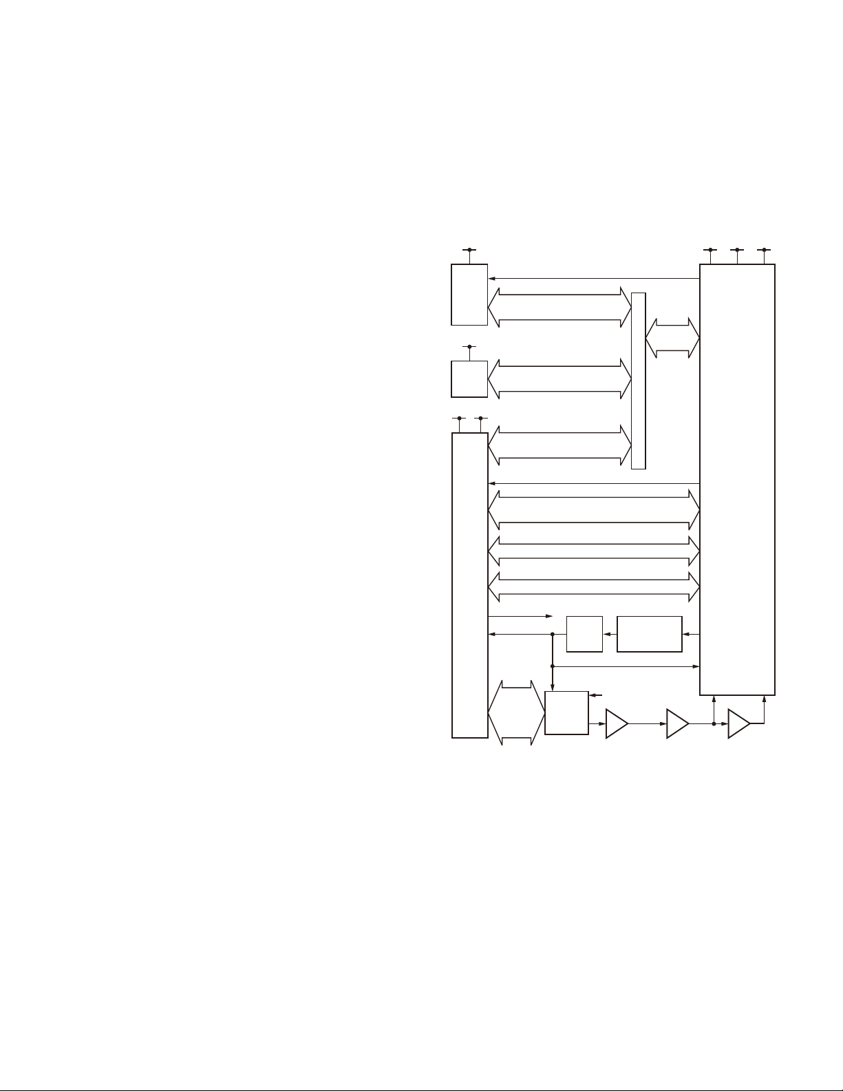
CIRCUIT DESCRIPTION
NXR-710
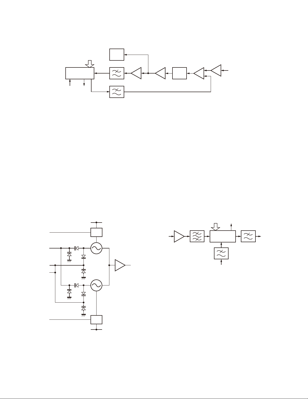
1. Outline
The NXR-710 is a VHF repeater operating in the 136~
174MHz frequency range.
2. TX-RX unit
TX-RX unit (X57-7940-10) consists of the following cir-
cuit.
(1) Internal/external reference circuit
(2) Transmitter reference 16.8MHz PLL circuit
(3) Transmitter main PLL circuit
(4) Modulation level adjustment circuit
(5) Front-end circuit
(6) 1st-Mixer circuit
(7) IF circuit
(8) Receiver PLL circuits
(9) AVR circuits
(10) Other circuits
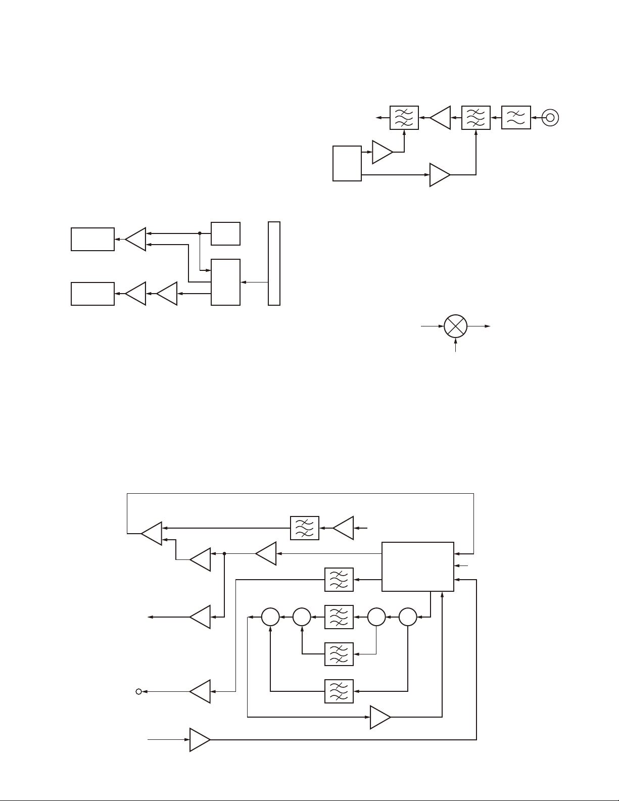
2-1. Internal/External reference circuit
The internal reference circuit consists of X500, Q502,
Q504 and D505. The output of 19.2MHz VCTCXO (X500) is
fed to buffer amplifi er Q502. The higher harmonic wave is
attenuated by the LPF. This reference signal is fed to IF IC
(IC304) as the 2nd Local signal through the Tripler.
The internal reference signal is amplified by Q504 to
achieve the needed level for PLL ICs. That signal is divided
by a Wilkinson divider. The divided signal is fed to the PLL
IC for the receiver. Another signal is fed to the transmitter
reference 16.8MHz PLL IC through PIN diode switch (D505)
which switches the Internal or external reference.
The external reference circuit consists of CN500, Q501,
Q503, IC500, IC501, D503 and D504. The external reference signal (10MHz/0dBm) input from CN500 is fed to buffer amplifi er Q501 and is amplifi ed by Q503. Q503 is a dual
gate MOS-FET. The output of amplifi er (Q503) is detected
by D503 and that DC voltage is amplified by IC500 (B/2).
The amplifi ed DC voltage is compared to the reference voltage by IC500 (A/2). The difference of voltages is amplifi ed
by IC500 (A/2) and is fed to the gate-2 terminal of Q503. The
voltage of the Q503 gate-2 terminal is controlled automatically to constantly maintain the power output of amplifier
(Q503). The output of amplifi er (Q503) is fed to the transmitter reference 16.8MHz PLL IC through the PIN diode switch
(D504) which switches the Internal or External reference.
The PIN diode switches (D504, D505) are controlled by
the I/O expander IC (IC805 Pin15). The I/O expander IC is
controlled by the MCU which is in the Control unit (X53-449).
If internal reference is selected by FPU, the I/O expander IC
outputs an “H” status. This signal sets power switch Q506
to ON. Then D505 is activated.
If external reference is selected, the I/O expander IC outputs an “L” status. This signal sets power switch Q500 to
ON. Then D504 is activated.
D503
Detector
REF
LPF
AGC AMP
1dB
ATT
1dB
ATT
10MHz or
19.2MHz
X58-5070-10
D504,D505
SW
RX VCO
/PLL
2nd Lo
Fig. 1 Internal/external reference circuit
2-2. Transmitter reference 16.8MHz PLL circuit
The transmitter reference 16.8MHz PLL circuit produces
the reference frequency signal for the Transmitter Main PLL
circuit and modulates the low-frequency components.
The circuit consists of IC600, IC601, IC602, IC603,
IC604, Q601, Q602, Q603, and X600.
The VCXO (X600) signal enters the buffer amplifi er Q603
and is amplifi ed by Q602. The higher harmonic wave is attenuated by the LPF and returns to IC602. Its phase is compared with that of the reference frequency 5kHz.
AMP
IC500(B/2)
Q503
AMP
Q504
X3
Q202LPF
phase is converted to a DC voltage by a lag-lead type loop
fi lter. This DC voltage is input to the IC604 invert amplifi er
and is synthesized with the modulating signal. This DC voltage is input to the X600 control voltage terminal for controlling the VCXO oscillating frequency 16.8MHz.
amplifi er. The output signal of the buffer amplifi er is used as
the reference frequency signal of the transmitter main PLL
circuit.
AMP
IC500(A/2)
EXT_IN
10MHz
Buffer
Q501
LPF
The phase difference signal produced by the comparing
The 16.8MHz oscillating signal is fed to the Q603 buffer
AMP
Q502
CN500
X500
OSC
19.2MHz
9
Page 10
NXR-710
CIRCUIT DESCRIPTION
SPSCLK0
/16_8PCS
IC602
MOD
PLL IC
Ref
LDT
10MHz
or 19.2MHz
SPSD0
X58-5080-10
TX VCO
/PLL
LPF
Loop filter
16.8MHz
AMP
Q602
Fig. 2 Transmitter reference 16.8MHz PLL circuit
2-3. Transmitter Main PLL circuit (SUB unit)
VCO
■
The TX VCO circuit consists of two VCOs (VCO A X58508: Q352, VCO B X58-508: Q353). Those VCOs generates
a transmit carrier. VCO A Q352 produces a transmitter frequency from 136.000MHz to 154.995MHz. VCO B Q353
produces a transmitter frequency from 155.000MHz to
174.000MHz.
Those VCO oscillation frequencies are determined by
two systems of voltage control terminals: “CV” and “TXASSIST”.
The voltage control terminals, “CV” and “TXASSIST”,
are controlled by the PLL IC (X58-508: IC300) and MCU
(X53-449: IC20) and the output frequency changes continuously according to the applied voltage. For the modulation
input terminal, “MO”, the output frequency changes according to the applied voltage.
80C
D358D359
SW Q350
VCO_A
Q352
VCO_B
Q353
Buffer
Q354
VO
TXVCOA
D355
TX_CV
D352
MO
TXASSIST
D357
Buffer
Q603
X600
OSC
16.8MHz
AMP
IC604
AMP
IC603
MB
minal and realizes the “Phase Locked Loop” for the return
control. This allows the VCO oscillation frequency to accurately match (lock) the desired frequency.
When the frequency is controlled by the PLL, the frequency convergence time increases as the frequency difference increases when the set frequency is changed. To
supplement this, the MCU is used before control by the
PLL IC to bring the VCO oscillation frequency close to the
desired frequency. As a result, the VCO CV voltage does not
change and is always stable at approx. 3.0V.
The desired frequency is set for the PLL IC by the MCU
(X53-449: IC20) through the 3-line “SPSD0”, “SPSCLK0”,
“/TXPCS” serial bus. Whether the PLL IC is locked or not is
monitored by the MCU through the “LDT” signal line. If the
VCO is not the desired frequency (unlock), the “LDT” logic
is low.
SPSCLK0
FIN
Buffer
Q300
SPSD0
/TXPCS
BPF
TX VCO/PLL
Ref 16.8MHz
IC300
LDT
Loop filter
TX_CV
LPF
Fig. 4 Transmitter Main PLL IC circuit
D353
D360D361
TXVCOB
SW Q351
80C
Fig. 3 Transmitter VCO circuit
PLL IC (X58-508: IC300)
■
The PLL IC compares the differences in phases of the
VCO oscillation frequency and the transmitter PLL reference
signal (16.8MHz), returns the difference to the VCO CV ter-
10
2-4. Modulation level adjustment circuit
The Modulation level adjustment circuit adjusts the modulation waveform balance. This circuit consists of IC804,
IC603, IC604, IC605 and IC606.
The modulating signal comes from the Control unit
(X53-449) through the interface connector (CN800 Pin 14).
The modulating signal is produced by the modulation lowpitched tone to the transmitter modulation 16.8MHz PLL circuit and adds the high-pitched modulation to the transmitter
main PLL.
IC804 is an electronic volume control IC. It has 8 electronic volume control circuits. The modulation level adjustment circuit uses 2 electronic volume control circuits in
IC804. The 1st electronic volume control circuit adjusts the
modulating signal and is fed to IC603 and the 2nd electronic
Page 11
CIRCUIT DESCRIPTION
NXR-710
volume control circuit. The 2nd electronic volume control
circuit adjusts the modulating signal and is fed to IC606.
IC603 is an inverting amplifi er for inverting the amplifi cation of the modulating signal. The output of IC603 and
the charge pump output of IC602 (Transmitter modulation
16.8MHz PLL IC) are synthesized by IC604 and is fed to
VCXO (X600).
IC606 is a non-inverting amplifi er. The output of the 2nd
electronic volume control circuit is amplifi ed by IC606 and is
fed to the transmitter main PLL circuit.
X58-5080-10
TX VCO
/PLL
X600
OSC
16.8MHz
AMP
IC606
AMP
IC604
AMP
IC603
VREF
IC605
MO
EVOL
IC804
MB
CN800
MOD
Fig. 5 Modulation level adjustment circuit
2-5. Front-end circuit
The front-end circuit consists of LPF, L111, L112, L114,
and L115 coils, former BPF tuning Variable Capacitance
Diodes (D105, D106, D107 and D108), RF amplifi er Q101
(LNA), L100, L101, L103, and L104 coils, and latter BPF
tuning Variable Capacitance Diodes (D100, D101, D103 and
D104). The BPF covers frequency ranges 136 to 174MHz.
The LPF, former and latter BPF attenuate the unwanted
signals receiving from RX antenna (CN101) and only the desired signals transmit to the 1st-mixer.
136~
174MHz
EVOL
IC804
BPF
Buffer
IC100
LNA AMP
Q101
Buffer
IC101
BPF LPF
RX ANT
CN101
136~
174MHz
Fig. 6 Front-end circuit
2-6. 1st-Mixer circuit
The signal passing the front-end circuit is heterodyned
with the fi rst local oscillator signal from the PLL frequency
synthesizer circuit at the first mixer (IC300) to become a
58.05 MHz fi rst intermediate frequency (IF) signal.
Mixer
IC300
136~174MHz
1st Local
194.05~232.05MHz
IF1
58.05MHz
Fig. 7 1st-Mixer circuit
2-7. IF circuit
The fi rst IF signal is amplifi ed by the IF Post Amp (Q301)
and passed through a four-pole monolithic crystal filter
(XF300) to reject adjacent channel signals. The fi ltered fi rst
IF signal is amplified by the IF AGC amplifier (Q300) and
then applied to the IF system IC (IC403). The IF system IC
IF AGC AMP
Q300
RSSI
450kHz
CN802
AGC
Diff AMP
IC401(B/2)
AMP
IC409(A/2,B/2)
IF AMP
IC400
Buffer
IC402
Buffer
IC401(A/2)
IC405
MCF
XF300
IC406
SW
SW
Fig. 8 IF circuit
POST AMP
Q301
CF400
CF402
CF403
CF401
58.05MHz
RSSI
IF2
IC408SWIC407
SW
IF AMP
IC404
IF IC
IC403
IF1
2nd Lo
57.6MHz
AGC
11
Page 12
NXR-710
CIRCUIT DESCRIPTION
provides a second mixer, AGC amplifi er, and RSSI (Received
Signal Strength Indicator).
The second mixer mixes the fi rst IF signal with the 57.6
MHz of the second local oscillator output and produces the
second IF signal of 450kHz.
The second IF signal is passed through the ceramic fi lter
(CF401, CF402 and CF403) to reject the adjacent channel
signal. The fi ltered second IF signal is amplifi ed by the second IF amplifi er (IC404) and AGC amplifi er (IC403).
The signal from the AGC amplifi er is input to the AD converter (X53-449: IC20) through the ceramic fi lter (CF400) and
operational amplifi er (IC400 and X53-449: IC20).
2-8. Receiver PLL circuit (SUB unit)
VCO
■
RX VCO circuit consists of two VCOs (VCO A X58507: Q352, VCO B X58-507: Q353). Those VCOs generate a 1st local signal. For the VCO oscillation frequency,
the 1st local signal is 194.05 to 232.05MHz. (VCO A:
194.05~213.05MHz, VCO B: 213.05~232.05MHz)
Those VCO oscillation frequencies are determined by
two systems of voltage control terminals: “CV” and “RXASSIST”.
The voltage control terminals, “CV” and “RXASSIST”,
are controlled by the PLL IC (X58-507: IC300) and the MCU
(X53-449: IC20) and the output frequency changes continuously according to the applied voltage.
80C
Q350
D358D359
D360D361
SW
VCO_A
Q352
VCO_B
Q353
Q351
Buffer
Q354
VO
RXVCOA/B
D355
RX_CV
D352
RXASSIST
D357
D353
Fig. 9 Receiver VCO circuit
PLL IC (X58-507: IC300)
■
PLL IC compares the differences in phases of the VCO
oscillation frequency and the VCTCXO reference frequency,
returns the difference to the VCO CV terminal and realizes
the “Phase Locked Loop” for the return control. This allows
the VCO oscillation frequency to accurately match (lock) the
desired frequency.
When the frequency is controlled by the PLL, the frequency convergence time increases as the frequency difference increases when the set frequency is changed. To
supplement this, the MCU is used before control by the
PLL IC to bring the VCO oscillation frequency close to the
desired frequency. As a result, the VCO CV voltage does not
change and is always stable at approx. 3.0V.
The desired frequency is set for the PLL IC by the MCU
(X53-449: IC20) through the 3-line “SPSD0”, “SPSCLK0”,
“/RXPCS_TR” serial bus. Whether the PLL IC is locked or
not is monitored by the MCU through the “LDR” signal line.
If the VCO is not the desired frequency (unlock), the “LDR”
logic is low.
Buffer
Q300
FIN
LPF
SPSCLK0
SPSD0
/RXPCS
RX VCO/PLL
IC300
Ref 19.2MHz
LDT
Loop filter
RX_CV
LPF
Fig. 10 Receiver PLL circuit
2-9. AVR circuit
The 13.6V Power Source (+B) is provided through the
Connector (CN701) from the Final unit (X45-392). +B is connected to a FET switch (Q702, Q703) and CN700. Q702
and Q703 are controlled by the “SBC” signal from the MCU
which is in the Control unit (X53-449). If “SBC” logic is
high, Q702 and Q703 turn on. The 13.6V power source (SB)
which is turned on by Q702 and Q703 is provided to the 8V
AVR IC (IC702) and CN700. CN700 is connected to the Control unit (X53-449) to provide the +B power source and the
SB power source.
IC702 supplies 8V to the VCO, 15V DC/DC converter IC
(IC701), AVR IC (IC700) and FET switches (Q700, Q701).
IC701 is a step-up switching regulator. IC701 regulates 8V
to 15V and supplies the 15V power source to the “assist circuit” and “front-end BPF tuning circuit”. The FET switches
(Q700, Q701) are controlled by the I/O expander IC (IC805).
When Q700 and Q701 turn on, the 8V power source is provided to receiver section.
IC700 regulates 5V to 8V. The output of IC700 is provided to the FET switches (Q705, Q706) and AVR IC (IC703).
The FET switches (Q705, Q706) are controlled by the I/O
expander IC (IC805). When Q705 and Q706 turn on, the 5V
power source is provided to the receiver section, IF section
and IC704. IC704 regulates 5V to 3V. The 3V power source
is provided to the Mixer IC (IC300). IC703 regulates 5V to
3.3V. The output of IC703 is provided to the IF section.
12
Page 13
CIRCUIT DESCRIPTION
NXR-710
+B
from Final unit
(X45-392 A/3)
+B,SB
to Control unit
(X53-449)
CN701
CN700
Q702,Q703
SW
SBC
SB
IC702
8V AVR
Fig. 11 AVR circuit
2-10. Other circuit
EEPROM
■
The EEPROM (IC802) has a data capacity of 2Kbit. It
stores the tuning data in frequency adjustment.
Temperature sensor
■
The temperature sensor (IC800) monitors temperature
around the VCTCXO (X500).
I/O expander
■
The I/O expander IC (IC805) controls power sources, fan,
analogue switches, and the transmit power control circuit.
IC805 is controlled by the MCU which is in the Control unit
(X53-449).
Electronic volume control IC
■
The Electronic volume control IC (IC804) adjusts the
modulating signal, center frequency of the front-end BPF,
and the power of the RF fi nal amplifi er. IC804 is controlled
by the MCU which is in the Control unit.
LPF
TX ANT
CM coupler
REV DET
D4
FW DET
D3
80C
IC701
Q700,Q701
SW
5V AVR
IC700
RXC
Q705,Q706
SW
RXC
3.3V AVR
IC703
Ripple Filter
Ripple Filter
Ripple Filter15V DC/DC
Ripple Filter
IC704
3V AVR
80C_1
80C_2
150C_1
150C_2
80R
50C
50R
30R
33C
3. Final unit
The RF final amplifier unit (X45-3920-10) amplifies the
transmitter power to a specifi ed level.
This unit consists of the following circuits:
(1) Driver and Final power amplifi er circuit
(2) CM coupler circuit
(3) Filter circuit
(4) APC circuit
(5) High temperature detector circuit
(6) FAN action control circuit
(7) AVR circuit
3-1. Driver and Final power amplifi er circuit
The transmit signal from the TX IN terminal CN1 of the
Final unit (X45-392) is amplifi ed by Q1, Q2 and Q3, and is
passed to the final stage Q4. The signal amplified by the
fi nal stage Q4 passes through the CM coupler circuit and
fi lter circuit, and is then fed to the antenna.
+B
Final AMP
Q4
Vcont
Auto power control
Drive AMP
Q3
Drive AMP
Q2
Limiter AMP
IC201(B/2)
80T
Drive AMP
Q1
80T
CN1
CN801
8TC
FAN
ASWC
PLIM
DC AMP
IC202(A/2)
Buffer AMP
REV DET
FW DET
IC202(B/2)
Fig. 12 Driver and Final power amplifi er circuit
PRE AMP
IC201(A/2)
RAMP
FDT
Temp1
TH201
13
Page 14
NXR-710
CIRCUIT DESCRIPTION
3-2. CM coupler circuit
The CM coupler circuit is a line for detecting forward
wave and refl ected wave. Forward wave is detected by D3,
and is converted into DC voltage. If an abnormal antenna
load is connected, reflected wave is detected by D4 and
converted into DC voltage.
3-3. Filter circuit
This circuit removes harmonics from the transmitter output and sends fi ltered signals to the antenna.
3-4. APC circuit
The automatic transmission power control (APC) circuit
stabilizers the transmitter output power at a pre-determined
level. DC voltage from the CM coupler circuit is amplifi ed by
the DC amplifi er IC202 (1/2). IC202 (2/2) compares the APC
control voltage (RAMP) generated by the MCU (X53-449)
and the DC amplifi er IC201 (1/2, 2/2) with the output voltage
from IC202 (1/2) to control the gate voltage for amplifi er Q3
and fi nal amplifi er Q4.
3-5. High temperature detector circuit
To prevent thermal destruction of amplifi er Q3 and fi nal
amplifier Q4, this circuit reduces the APC control voltage
(RAMP) when the temperature of amplifi er Q3 and fi nal amplifi er Q4 rises. The MCU detects the temperature with the
thermistor (TH201) and controls the APC voltage (RAMP).
3-6. FAN action control circuit
The FAN action control circuit consists of the FAN and
switching transistor Q207. It is controlled by the MCU (X53-
449). If the FAN action is set to “Temperature”, the cooling
fan is turned ON or OFF according to temperature. If the
FAN action is set to “Continuous”, the cooling fan operates
continuously, but Q207 stays ON.
3-7. AVR circuit
The 13.6V power source (+B) is provided through connector CN201 to the Final unit (X45-392 A/3). +B is connected to CN203 to supply the 13.6V power source for the
TX-RX unit (X57-794). +B is a power source for the “fi nal
amplifi er”, “drive amplifi er” and fan. IC203 regulates the +B
voltage to 8V. This 8V power source is connected to the FET
switches Q203, Q204, Q205, and Q206. Q204 and Q206
are controlled by the “8TC” signal from the I/O expander IC
which is in the TX-RX unit (X57-794). If “8TC” logic is high,
Q204 and Q206 turn on and supply the 8V power source
to the APC circuit and pre drive amplifi ers. Q203 and Q205
are controlled by the “ASWC” signal from the I/O expander
IC which is in the TX-RX unit (X57-794). If “ASWC” logic
is high, Q203 and Q205 turn on and supply the 8V power
source to the antenna switch circuit.
+B
from Final unit
(X45-392 B/3)
+B
to TX-RX unit
(X57-794)
CN201
CN203
Fig. 13 AVR circuit
4. Control unit
The Control unit (X53-4490-10) consists of the following
circuits:
(1) MCU circuit
(2) Memory circuit
(3) DSP circuit
(4) Squelch circuit
(5) Power supply circuit
(6) Power Supply Voltage Monitoring Circuit
(7) 18.432MHz clock circuit
(8) Audio circuit
(9) Other circuit
Final AMP
Drive AMP
IC203
8V AVR
Q204,Q206
SW
8TC
Q203,Q205
SW
ASWC
FAB
80T
80SW
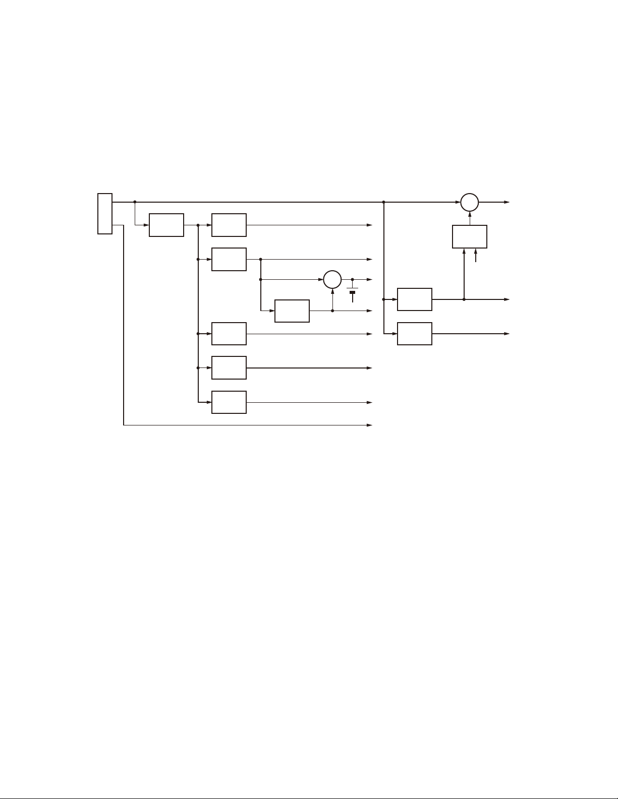
4-1. MCU circuit
The MCU (IC20) is a 32bit RISC processor, equipped with
a peripheral function and ADC/DAC.
This MCU operates at a 18.432MHz clock and 3.3V/1.5V
DC.
It controls the fl ash memory, SRAM, DSP, receive circuit,
transmitter circuit, and control circuit.
14
Page 15
CIRCUIT DESCRIPTION
NXR-710
4-2. Memory circuit
The Memory circuit consists of the MCU (IC20), the
SRAM (IC9), and the fl ash memory (IC3).
The fl ash memory has a capacity of 32Mbit that contains
the transceiver control program for the MCU and stores the
data. It also stores the data for transceiver channels and
operating parameters that are written by the FPU. This program can be easily written from external devices.
The SRAM has a capacity of 1Mbit that contains work
area and data area.
Flash memory
■
Note: The fl ash memory stores the data that is written by
the FPU, tuning data (Deviation, Squelch, etc.), and firmware program.
SRAM (static memory)
■
Note: The SRAM has a temporary data area and work area.
When the power supply is off, it is backed up by an internal
secondary lithium battery. Therefore, the saved data is not
lost.
4-3. DSP circuit
The DSP circuit consists of a DSP (IC6) and processes
the base band signal. The DSP operates on an external clock
of 18.432MHz (the same as IC20). The I/O section operates
at 3.3V and the core section operates at 1.6V. The DSP carries out the following processes:
Digital processing
■
• 4Level FSK and Baseband fi lter processing
• Vocoder processing between audio codec and modula-
tion/demodulation
• CAI processing, such as error correction encoding/decod-
ing and interleaving
• AFC loop control
• Frame synchronization and Time tracking
• Data scrambling
Analog FM processing
■
• Pre-emphasis/De-emphasis
• QT/DQT encoding/decoding
• DTMF encoding/decoding
• Compressor/Expander processing
• Voice scrambler processing
4-4. Squelch circuit
The Squelch circuit amplifi es the demodulated noise signal from IC6 after fi ltering through the BPF circuit. The processed digital noise signal is applied to CODEC IC14, and is
converted from digital to analog. The amplifi ed signal is then
converted to a DC signal by the detection circuit. The converted signal is fed back to IC20.
33M 33M 33A15M
FLASH
IC3
33BU
SRAM
IC9
33M 16M
DSP
IC6
/FRST
A[0~21], D[0~15],
/RD, /WR, /CS0, /WP
A[0~17], D[0~7],
/RD, /WR, /CS2
A[0~20], D[0~15], /RD,
/WR, /HRDY, /CS3, /HDS2
/DRST
/MCCSXCN, /MCCSRCN, MCDICN,
MCDOCN, MCSCKCN
MCSCKAF, /MCCSAF, MCDIAF, MCDOAF
/SYMTIM, /DINT, /DWUP, FSDET, /HINT
/PCS_DSP
MAIN_CLK
/PDN,
LRCLK,
SDTI,
BICLK
Buffer
IC16
Squelch
DAC
IC14
VCTCXO
X1
(18.432MHz)
VREF
AMP
IC13(A/2,B/2)
AMP
Q4
/FRST
MCU
IC20
/DRST
BSHIFT
XTAL_IN
LDR
IC15(A/2)
ADC1
AMP
Fig. 14 Control circuit
Audio or Modulation function
■
• Transmit/Receive audio fi ltering processing
• Microphone amplifi er AGC processing
• Audio soft mute processing
• Modulation level processing
• Squelch Filtering
Other function
■
• Voting tone
• CWID
• Courtesy tone
• Repeater operating
• Analog/Digital Mixed mode
4-5. Power supply circuit
The X53-449 circuit consists of IC301, IC302, IC303,
IC304, IC305 and IC306.
IC301 is a DC/DC converter that converts 13.6V to 6.0V.
This 13.6V voltage is supplied from TX-RX unit (X57-794).
IC302 is connected to IC301 and regulates the voltage
to 5.0V. IC303, IC304, IC305 and IC306 are connected to
IC301. IC303 and IC306 are 3.3V voltage regulators. IC304
is a 1.5V regulator IC, and IC305 is a 1.6V regulator IC.
CN302 is the connector for the lithium battery. The
lithium battery is used to back up the SRAM and RTC data
when no external DC power source is available.
15
Page 16
NXR-710
CIRCUIT DESCRIPTION
4-6. Power supply voltage monitoring circuit
The X53-449 circuit consists of IC307, IC308, D303 and
Q301.
IC308 is a voltage detect IC and is used to generate the
“/RST” signal for the MCU (IC20).
This “/RST” signal is connected to the hardware reset
pin of MCU (IC20).
CN301
B
SB
DC-DC
IC301
60DC
IC302
IC303
IC305
IC304
AVR
AVR
AVR
AVR
50M
33M
16M
15M
RESET
IC308
IC307 is a voltage detect IC and is used to generate the
“/BINT” signal for the MCU (IC20).
This “/BINT” signal is connected to the hardware interrupt pin of MCU (IC20). The software of the MCU (IC20)
runs to the sleep-mode to use the “/BINT” signal.
D303 and Q301 are used to generate the “OVRB” signal
for the MCU (IC20). The software of the MCU (IC20) runs to
the sleep-mode to use the “OVRB” signal.
AMP_B
SW
Q402
OR
Q401
Q303
/RST
SW
33BU
/OVRB
Q301
/BINT
IC307
/OVRB
/BINT
AMP_SW
33A
AVR
IC306
Fig. 15 Power supply circuit
4-7. 18.432MHz clock circuit
The 18.432MHz clock is provided to the MCU (IC20),
DSP(IC6), and DAC (IC14) of the Squelch circuit.
4-8. Audio circuit
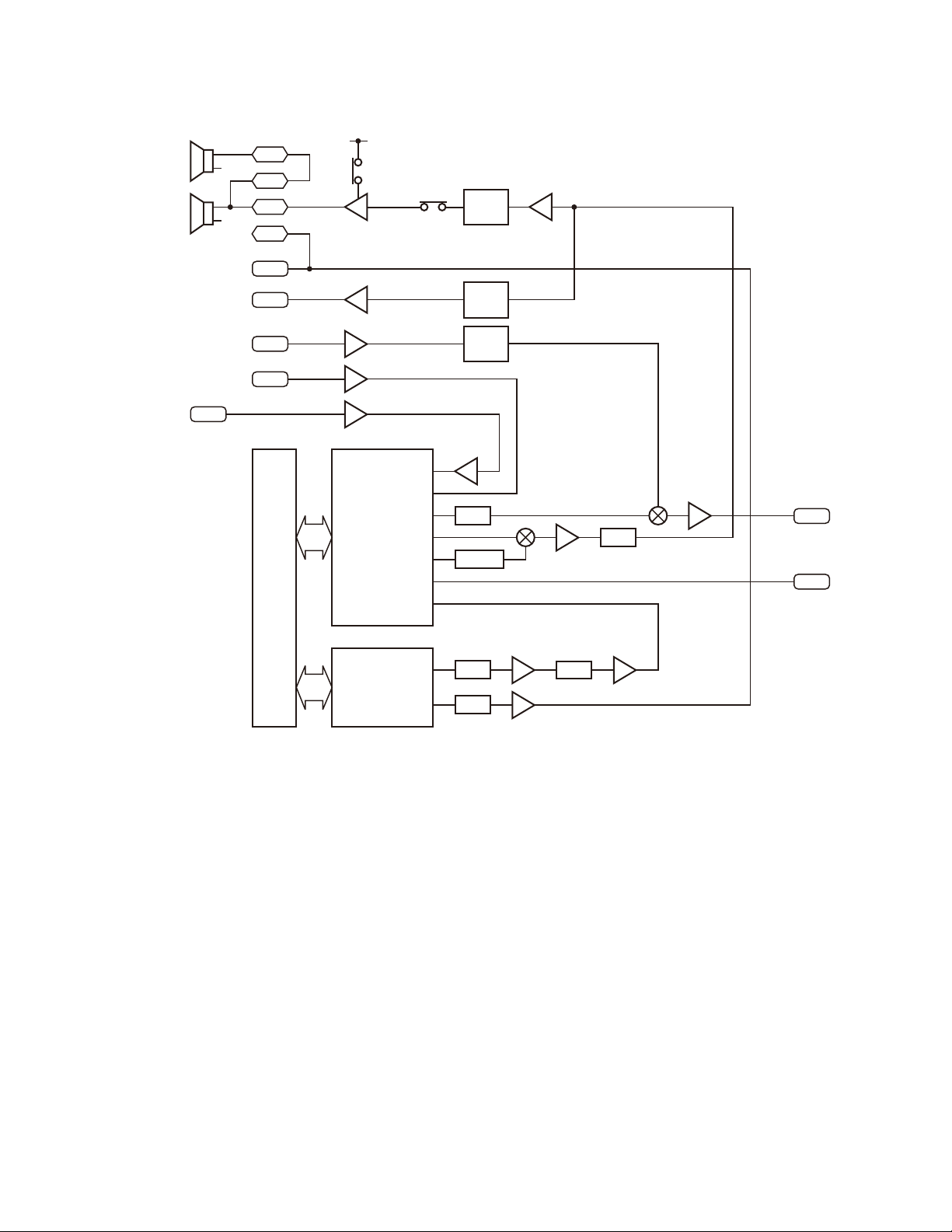
Audio amplifi er circuit
■
The audio amplifi er circuit is located in the control section of the Control unit (X53-449). The 4W output audio
power is available from the pin 15 TEST/SPKR connector
“SPO”, “SPG” on the rear panel to the external speaker in
the case of a power supply voltage of 13.6V and a 4Ω load.
Microphone circuit
■
The signal from the microphone is passed through the
AGC circuit located in the Display unit (X54-358 A/2) so that
it may not saturate. This circuit consists of IC501, D501,
D502 Q501, and Q502. The AGC controls the amplifi er gains
using the detected audio signal depending on the positive
and negative peaks of the signal amplitude. The audio signal goes to the control section of the Control unit (X53-449)
from the Display unit (X54-358 A/2).
Modulation circuit (Analog/Digital signal processing)
■
In the case of the Analog Signal Processing mode, the
transmitting audio signal is amplifi ed by IC405 (C/4), input to
the MICADCO terminal of the MCU (IC20), and audio processed by DSP (IC6). The processed audio signal from the
MODDAC terminal of IC20 is passed through an anti-aliasing
fi lter at IC404 (A/2), and is then amplifi ed to a suffi cient level
by IC404 (B/2), and amplifi ed by the summing (TD) amplifi er.
The Digital Signal Processing mode is the same as the Analog Signal Processing mode.
4-9. Other circuit
Real-time clock
■
The clock function is based on a real-time clock IC (IC17).
When the power supply is off, it is backed up by an internal
secondary lithium battery.
16
Page 17
CIRCUIT DESCRIPTION
NXR-710
INT_SP
EXT_SP
MIC
SPO
SPI
SPO
RD
RD
RA
TD
TA
DSP
IC6
AMP_B
AMP_SW
Audio_AMP
IC501
MICADC0
MICADC1
MODDAC
MCU
IC20
SPDAC
PWM1
IFR
ADC1
SW
IC402
IC412
IC412
IC412
IC405
(C/4)
LPF
CR-LPF
DAC
DAC
DAC
IC404(A/2)
LPF
IC404
(B/2)
MOD
IF
signal
MOD
Squelch DAC
IC14
Fig. 16 Modulation circuit (Analog/Digital signal processing)
5. Display unit
The Display unit (X54-3580-20) is the same circuit as
X54-3580-20, used in TKR-750/850/751/851.
The Display unit (X54-3580-20) consists of the following
circuits:
(1) LED circuit
(2) Key switch circuit
LPF
LPF
DET
5-1. LED circuit
The display circuit consists of various types of LEDs:
7-segment type D506 and D507 (red), D503 (red: transmission), D504 (green: busy), D505 (green: power on).
IC502 to IC505 are shift registers that convert MCU serial data to parallel data and turn on LEDs.
5-2. Key switch circuit
There are PF key 1 to PF key 6 on Display unit. Using
these key switches, mode settings are available.
The logic signals pushing these key switches are entered
directly into the MCU (IC20).
17
Page 18
NXR-710
COMPONENTS DESCRIPTION
FINAL UNIT (X45-3920-10)
Ref. No. Part Name Description
IC201,202 MOS-IC DC amplifi er
IC203 Analogue IC Voltage regulator
Q1,2 Transistor RF amplifi er
Q3 FET TX drive amplifi er
Q4 FET Final amplifi er
Q203~206 FET DC switch
Q207 Transistor DC switch
D1 Diode RF switch
D3,4 Diode RF detector
D7,8 Diode RF switch
D9 Surge absorber Surge protection
D10 Diode RF detector
D201 Zener diode Voltage reference
D202 Surge absorber Surge protector
D203 Diode Surge protector
D301 Diode Protect of reverse connection
CONTROL UNIT (X53-4490-10)
Ref. No. Part Name Description
IC3 ROM IC Flash memory
IC4,5 MOS-IC RS-485 transceiver
IC6 Microprocessor IC DSP
IC7,8 MOS-IC Buffer
IC9 SRAM IC SRAM
IC10,11 MOS-IC Buffer
IC12 MOS-IC AND gate
IC13 MOS-IC AF amplifi er
IC14 MOS-IC CODEC
IC15 MOS-IC AF amplifi er
IC16 MOS-IC Buffer amplifi er
IC17 MOS-IC RTC IC
IC18,19 MOS-IC Buffer
IC20 MOS-IC MCU
IC21 MOS-IC RS-232C driver/receiver
IC22 MOS-IC I/O expander
IC23 MOS-IC NAND gate
IC24 MOS-IC AND gate
IC25 MOS-IC OR gate
IC26 MOS-IC AND gate
IC27,28 MOS-IC AF amplifi er
IC301 Analogue IC DC/DC converter
IC302 MOS-IC Voltage regulator
IC303~306 Analogue IC Voltage regulator
IC307 MOS-IC Voltage regulator
IC308 Analogue IC Voltage regulator
18
Ref. No. Part Name Description
IC401 MOS-IC NAND gate
IC402 MOS-IC Analog switch
IC403 Bi-polar IC AF power amplifi er
IC404~406 Bi-polar IC OP AMP
IC407 MOS-IC Analog switch
IC411 Bi-polar IC OP AMP
IC412 MOS-IC DC/AC converter
Q4 Transistor DC switch
Q5 FET DC switch
Q6~10 Transistor Buffer amplifi er
Q301 Transistor DC switch
Q302 FET DC switch
Q303 Transistor Power switch
Q401 Transistor Power switch
Q402 FET Power switch
Q403 Transistor Power switch
Q404,405 Transistor AF mute switch
D1,2 Diode Detector
D3~12 Diode Surge protector
D13 Zener diode Surge protector
D14~16 Diode Surge protector
D18 Diode Surge protector
D20 Diode Surge protector
D22,23 Diode Surge protector
D24 Zener diode Surge protector
D26 Diode Surge protector
D28,29 Diode Surge protector
D30 Zener diode Surge protector
D31 Diode Surge protector
D32 Zener diode Surge protector
D35 Diode Surge protector
D36 Zener diode Surge protector
D37 Varistor Current protector
D301,302 Diode Surge protector
D303 Zener diode Voltage reference
D304,305 Diode Surge protector
D401 Diode Diode switch
DISPLAY UNIT (X54-3580-20)
Ref. No. Part Name Description
IC501 MOS IC MIC amplifi er
IC502~505 MOS IC Shift register
IC506,507 MOS IC Voltage regulator
Q501,502 Transistor Level controller
Q503,504 FET DC switch
Q506 Transistor DC switch
Page 19
COMPONENTS DESCRIPTION
NXR-710
Ref. No. Part Name Description
Q507 FET DC switch
Q508~511 Transistor DC switch
Q512~514 FET DC switch
Q516~519 FET DC switch
Q521~525 FET DC switch
D501,502 Diode AF detector
D503~507 LED LED
D508~514 Diode Surge absorption
D601,602 Diode Surge absorption
D603 Varistor Current protector
TX-RX UNIT (X57-7940-10)
Ref. No. Part Name Description
IC100,101 MOS-IC OP AMP
IC200,201 MOS-IC OP AMP
IC203 MOS-IC Buffer
IC300 MOS-IC Mixer
IC400 MOS-IC IF amplifi er
IC401 MOS-IC Buffer amplifi er
IC402 MOS-IC OP AMP
IC403 MOS-IC IF system
IC404 MOS-IC IF amplifi er
IC405~408 MOS-IC Analog switch
IC409 MOS-IC Buffer amplifi er
IC500 MOS-IC Buffer amplifi er
IC501 MOS-IC OP AMP
IC600,601 MOS-IC Buffer
IC602 MOS-IC 16.8MHz PLL
IC603~607 MOS-IC OP AMP
IC608 MOS-IC AF amplifi er
IC700~702 Analogue IC Voltage regulator
IC703,704 Bi-polar IC Voltage regulator
IC800 MOS-IC Temperature sensor
IC801 MOS-IC OP AMP
IC802 ROM IC EEPROM
IC803 MOS-IC Buffer amplifi er
IC804 MOS-IC Digital potentiometer
IC805 MOS-IC I/O expander
IC806 MOS-IC Analog switch
Q100 Transistor DC switch
Q101 Transistor RF amplifi er
Q200,201 Transistor DC switch
Q202,203 Transistor RF amplifi er
Q300 FET RF amplifi er
Q301 Transistor RF amplifi er
Q500 FET DC switch
Ref. No. Part Name Description
Q501 Transistor RF amplifi er
Q502,503 FET RF amplifi er
Q504 Transistor RF amplifi er
Q505~507 FET DC switch
Q600 FET DC switch
Q601 Transistor DC switch
Q602,603 Transistor RF amplifi er
Q604,605 Transistor DC switch
Q606 Transistor RF amplifi er
Q607 FET DC switch
Q700~702 FET DC switch
Q703 Transistor DC switch
Q704~706 FET DC switch
Q800 FET DC switch
D100,101 Varicap Frequency control
D103~108 Varicap Frequency control
D200 Diode DC switch
D500,501 Zener diode Limiter
D503 Diode Detector
D504,505 Diode RF switch
D600 Diode DC switch
D601 Diode RF switch
D801 Diode DC switch
RX VCO/PLL UNIT (X58-5070-10)
Ref. No. Part Name Description
IC300 IC PLL
Q300 Transistor Buffer amplifi er
Q350,351 FET DC switch
Q352,353 FET VCO OSC
Q354 Transistor Buffer amplifi er
D352,353 Varicap Frequency control
D355 Varicap Frequency control
D357~361 Varicap Frequency control
TX VCO/PLL UNIT (X58-5080-10)
Ref. No. Part Name Description
IC300 IC PLL
Q300 Transistor Buffer amplifi er
Q350,351 FET DC switch
Q352,353 FET VCO OSC
Q354 Transistor Buffer amplifi er
D352,353 Varicap Frequency control
D355 Varicap Frequency control
D357~361 Varicap Frequency control
19
Page 20
NXR-710
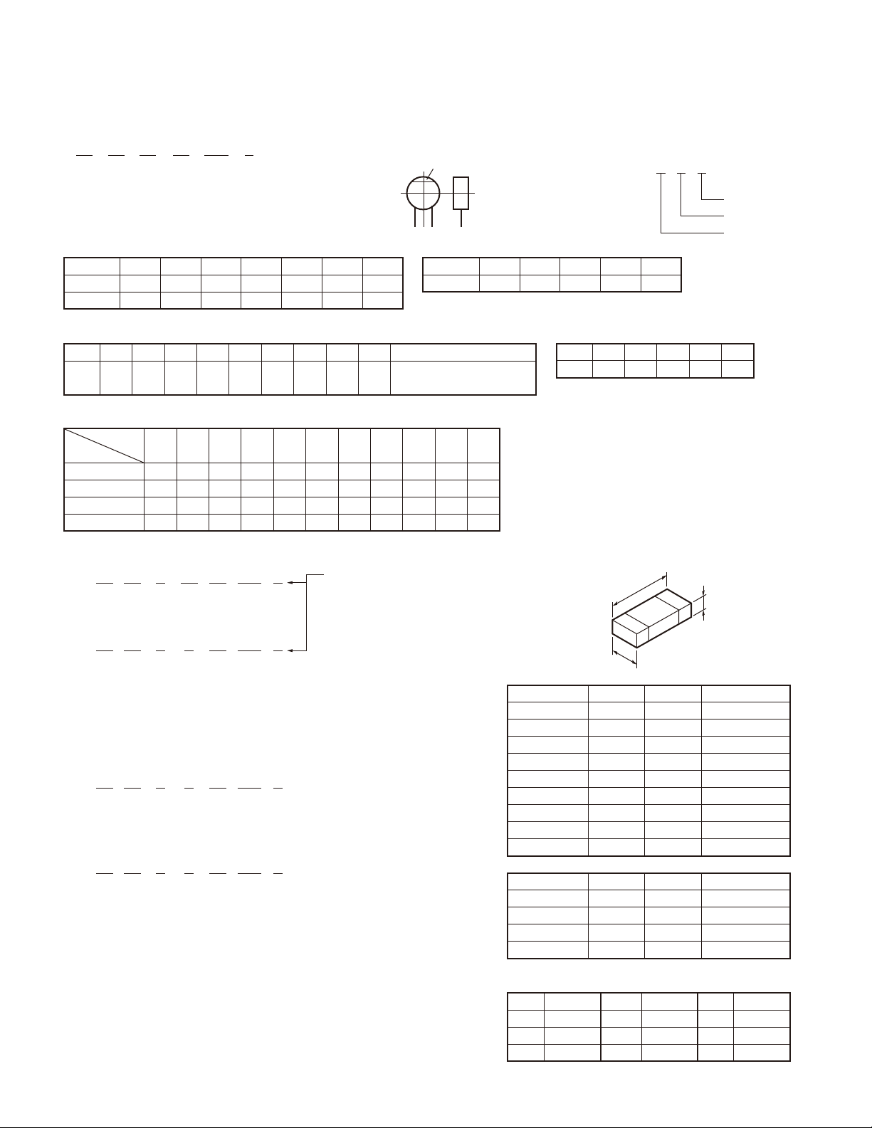
CAPACITORS
C C 4 5 T H 1 H 2 2 0 J
1 2 3 4 5 6
1 = Type ... ceramic, electrolytic, etc. 4 = Voltage rating
2 = Shape ... round, square, etc. 5 = Value
3 = Temp. coefficient 6 = Tolerance
• Temperature coefficient
1st Word C L P R S T U
Color* Black Red Orange Yellow Green Blue Violet
ppm/°C 0 –80 –150 –220 –330 –470 –750
PARTS LIST
CC45
Color*
2nd Word G H J K L
ppm/°C ±30 ±60 ±120 ±250 ±500
Example : CC45TH = –470±60ppm/°C
• Capacitor value
010 = 1pF 2 2 0 = 22pF
100 = 10pF
101 = 100pF Multiplier
102 = 1000pF = 0.001μF 2nd number
103 = 0.01μF 1st number
• Tolerance (More than 10pF)
Code C D G J K M X Z P No code
(%) ±0.25 ±0.5 ±2 ±5 ±10 ±20 +40 +80 +100 More than 10μF : –10~+50
–20 –20 –0 Less than 4.7μF : –10~+75
• Voltage rating
2nd word
A B C D E F G H J K V
1st word
0 1.0 1.25 1.6 2.0 2.5 3.15 4.0 5.0 6.3 8.0 –
1 10 12.5 16 20 25 31.5 40 50 63 80 35
2 100 125 160 200 250 315 400 500 630 800 –
3 1000 1250 1600 2000 2500 2150 4000 5000 6300 8000 –
• Chip capacitors
(EX) C C 7 3 F S L 1 H 0 0 0 J Refer to the table above.
1 2 3 4 5 6 7 1 = Type
(Chip) (CH, RH, UJ, SL) 2 = Shape
3 = Dimension
(EX) C K 7 3 F F 1 H 0 0 0 Z 4 = Temp. coefficient
1 2 3 4 5 6 7 5 = Voltage rating
(Chip) (B, F) 6 = Value
7 = Tolerance
RESISTORS
• Chip resistor (Carbon)
(EX) R D 7 3 E B 2 B 0 0 0 J
1 2 3 4 5 6 7
(Chip) (B, F)
• Carbon resistor (Normal type)
(EX) R D 1 4 B B 2 C 0 0 0 J
1 2 3 4 5 6 7
1 = Type 5 = Rating wattage
2 = Shape 6 = Value
3 = Dimension 7 = Tolerance
4 = Temp. coefficient
• Dimension
Chip capacitor
Code L W T
Empty 5.6±0.5 5.0±0.5 Less than 2.0
A 4.5±0.5 3.2±0.4 Less than 2.0
B 4.5±0.5 2.0±0.3 Less than 2.0
C 4.5±0.5 1.25±0.2 Less than 1.25
D 3.2±0.4 2.5±0.3 Less than 1.5
E 3.2±0.2 1.6±0.2 Less than 1.25
F 2.0±0.3 1.25±0.2 Less than 1.25
G 1.6±0.2 0.8±0.2 Less than 1.0
H 1.0±0.05 0.5±0.05 0.5±0.05
Chip resistor
Code L W T
E 3.2±0.2 1.6±0.2 1.0
F 2.0±0.3 1.25±0.2 1.0
G 1.6±0.2 0.8±0.2 0.5±0.1
H 1.0±0.05 0.5±0.05 0.35±0.05
• Rating wattage
Code Wattage Code Wattage Code Wattage
1J 1/16W 2C 1/6W 3A 1W
2A 1/10W 2E 1/4W 3D 2W
2B 1/8W 2H 1/2W
(Less than 10pF)
Code B C D F G
(pF) ±0.1 ±0.25 ±0.5 ±1 ±2
L
T
W
20
Page 21
PARTS LIST
NXR-710
New Parts.
✽
Parts without Parts No. are not supplied.
Les articles non mentionnes dans le Parts No. ne sont pas fournis.
Teile ohne Parts No. werden nicht geliefert.
Ref. No.
indicates safety critical components.
New
Ad dress
Parts No. Description
parts
NXR-710
1 3A ✽ A62-0933-23 PANEL ASSY (INNER)
2 1A A62-1146-04 PANEL (TX-RX)
3 1B A62-1147-04 PANEL (FINAL)
4 1D A62-1148-03 PANEL (OUTER)
5 3C ✽ A62-1174-03 PANEL ASSY
6 2C ✽ A82-0077-02 REAR PANEL
8 1F B10-2635-04 FRONT GLASS ACCESSORY
9 1F B11-1259-04 FILTER ACCESSORY
10 1F ✽ B62-2199-00 INSTRUCTION MANUAL
11 2C,3D ✽ B72-2596-04 MODEL NAME-PLATE
13 1B E30-3414-05 DC CORD (EXT DC IN)
14 1C E30-3418-15 ANTENNA CABLE (RX IN)
15 1E E30-3427-35 DC CORD ACCESSORY
16 1D E30-7528-15 ANTENNA CABLE (TX OUT)
17 1A ✽ E30-7689-05 TRUNK CABLE (X57-X53)
18 1C ✽ E30-7690-05 ANTENNA CABLE (REF IN)
19 1E E31-3228-05 15P PLUG ACCESSORY
20 1B ✽ E37-0902-15 LEAD WIRE WITH TERMINAL (DC+)
21 1B ✽ E37-0903-15 LEAD WIRE WITH TERMINAL (DC-)
22 3A E37-0905-15 LEAD WIRE WITH CONNECTOR (SP)
Desti-
nation
L : Scandinavia K : USA P : Canada
Y : PX (Far East, Hawaii) T : England E : Eu rope
C : China X : Australia M : Oth er Areas
NXR-710
FINAL UNIT (X45-3920-10)
Ref. No.
62 2B ✽ J19-5540-03 HOLDER (TRUNK CABLE)
63 1B J21-8467-04
64 1F J21-8559-04
66 1E J59-0302-05 GROMMET ACCESSORY
67 1B,1E J61-0307-05 BAND
69 1E K01-0418-15 HANDLE ACCESSORY
70 3A K29-5389-03 KNOB (VOLUME)
71 3A K29-9106-04 KNOB (POWER)
72 3A K29-9370-02 KEY TOP
74 1E L79-1419-05 LINE FILTER (ACCESSORY DC CORD)
75 1B L79-1854-05 LINE FILTER (DC CORD:EXT DC IN)
76 1B L79-1855-05 LINE FILTER (DC+,DC-)
A 2C N09-2292-05 HEXAGON HEAD SCREW (DSUB)
B
C 2A,1E N30-4006-48
D 2B,2C N30-4014-48
E 1C N30-4020-43 PAN HEAD MACHINE SCREW (FAN)
F 1C,2C N32-3006-48
G 3B N32-4008-43
H
J 1C N35-4006-43
K 1B,3B N67-3008-48
New
Ad dress
1C,2C,2D
N30-2606-48 PAN HEAD MACHINE SCREW (ANT)
1A,1B,1E
N35-3006-43
Parts No. Description
parts
MOUNTING HARDWARE (X45:DRIVE FET)
MOUNTING HARDWARE ACCESSORY
PAN HEAD MACHINE SCREW (CHAS,ACC)
PAN HEAD MACHINE SCREW (CHASSIS)
FLAT HEAD MACHINE SCREW (R PANEL)
FLAT HEAD MACHINE SCREW (F PANEL)
BINDING HEAD MACHINE SCREW (TOP,ACC)
BINDING HEAD MACHINE SCREW (TOP)
PAN HEAD SEMS SCREW (X53:AUDIO IC)
Destination
23 3A E37-0906-05
24 3A,2B E37-0908-05 LEAD WIRE WITH CONNECTOR (11P)
25 3A,1B E37-0911-05 LEAD WIRE WITH CONNECTOR (3P)
26 2B ✽ E37-0912-15 LEAD WIRE WITH MINIPIN PLUG
27 2C E37-0913-05
28 2A E37-1340-15 FLAT CABLE
29 2C E37-1376-05
32 1C,1E F05-1537-05 BLADE FUSE (15A/32V) ACCESSORY
33 2C F09-0445-05 CAP (DSUB)
34 1C F09-0471-15 FANMOTOR
36 1B ✽ F10-3129-03 SHIELDING CASE (X45 FINAL PCB)
38 2A,2B G02-0576-14 FLAT SPRING
39 2B G02-0829-14 FLAT SPRING (RX VCO)
40 3A G02-0885-13 EARTH SPRING (X54 DISPLAY PCB)
41 1B G02-0894-04 EARTH SPRING (X45:FINAL FET)
42 2B G02-1831-04 EARTH SPRING (REAR BOTTOM)
43 1C G02-1832-04 EARTH SPRING (REAR TOP)
44 1B ✽ G02-1855-04 FLAT SPRING (X45:AVR)
46 2B,3B G10-1263-04 FIBROUS SHEET (CHASSIS)
47 3C,2D G10-1264-04 FIBROUS SHEET (PANEL ASSY)
48 3B G10-1344-04
49 3B G10-1345-04
50 1F G13-1801-04 CUSHION (40X40X5) ACCESSORY
51 1F G13-1802-04 CUSHION (40X40X10) ACCESSORY
52 2B G13-1886-04 CUSHION (BNC)
54 1E H25-0029-04 PROTECTION BAG (60/110/0.07)
55 1F H25-0747-04 PROTECTION BAG (250X350)
56 1E H25-0762-04 PROTECTION BAG (120X300)
57 1F H25-2328-04 PROTECTION BAG (80/250/0.07)
58 1F ✽ H52-2334-02 ITEM CARTON CASE
LEAD WIRE WITH CONNECTOR (X53-X54)
LEAD WIRE WITH CONNECTOR (ACC15P)
LEAD WIRE WITH CONNECTOR (DSUB25P)
FIBROUS SHEET (EARTH SPRING,SHORT)
FIBROUS SHEET (EARTH SPRING,LONG)
L 1C,2C N80-2608-43 PAN HEAD TAPTITE SCREW (FUSE)
M 3A N87-3005-43 BRAZIER HEAD TAPTITE SCREW (SP)
N
78 3A T07-0770-35 SPEAKER
80 3A W09-0971-05 LITHIUM CELL
- 490-0174-05 ADHESIVE TAPE
3A,1B,2B
N87-3006-48 BRAZIER HEAD TAPTITE SCREW (PCB)
FINAL UNIT (X45-3920-10)
C4 CK73GB1H104K CHIP C 0.10UF K
C5-7 CK73GB1H102K CHIP C 1000PF K
C10 CK73GB1H102K CHIP C 1000PF K
C12 CC73GCH1H180J CHIP C 18PF J
C14 CK73GB1H102K CHIP C 1000PF K
C16-18 CK73GB1H102K CHIP C 1000PF K
C19 CC73FCH1H120J CHIP C 12PF J
C21 CK73GB1H102K CHIP C 1000PF K
C23 CK73GB1H102K CHIP C 1000PF K
C24 CK73FB1H102K CHIP C 1000PF K
C25 CC73FCH1H270J CHIP C 27PF J
C26 CC73FCH1H390J CHIP C 39PF J
C27 CC73FCH1H560J CHIP C 56PF J
C28 CK73FB1H102K CHIP C 1000PF K
C33 C93-0603-05 CHIP C 1000PF K
C34 ✽ C93-1744-05 CHIP C 470PF J
C37 CK73GB1E105K CHIP C 1.0UF K
C43 CC73GCH1H220J CHIP C 22PF J
C44 CC73GCH1H101J CHIP C 100PF J
C45 C93-0603-05 CHIP C 1000PF K
60 1E J02-0475-05 FOOT ACCESSORY
61 1E J02-0492-04 FOOT (RUBBER) ACCESSORY
C51 C93-0603-05 CHIP C 1000PF K
C52 ✽ C93-0868-15 MICA 240PF J
21
Page 22

NXR-710
FINAL UNIT (X45-3920-10)
Ad dress
New
Parts No. Description
parts
Ref. No.
C53 CK73GB1E105K CHIP C 1.0UF K
C54 ✽ C93-1747-05 CHIP C 130PF J
C57 ✽ C93-1800-05 CHIP C 82PF J
C60 CK73GB1H102K CHIP C 1000PF K
C61 CC73GCH1H220J CHIP C 22PF J
PARTS LIST
Destination
Ref. No.
Ad dress
L3 L41-5678-14 SMALL FIXED INDUCTOR (56NH)
L4 L41-6878-14 SMALL FIXED INDUCTOR (68NH)
L5 L41-2778-14 SMALL FIXED INDUCTOR (27NH)
L6 L41-1278-14 SMALL FIXED INDUCTOR (12NH)
L7 L41-1878-14 SMALL FIXED INDUCTOR (18NH)
New
Parts No. Description
parts
Destination
C63 ✽ C93-1790-05 CHIP C 33PF 500WV
C65 CC73GCH1H101J CHIP C 100PF J
C66 CK73GB1H102K CHIP C 1000PF K
C68 CM73F2H471J CHIP C 470PF J
C69 CK73GB1H102K CHIP C 1000PF K
C71 CK73GB1H102K CHIP C 1000PF K
C75 C93-0603-05 CHIP C 1000PF K
C78 CM73F2H471J CHIP C 470PF J
C80 CC73FCH1H270J CHIP C 27PF J
C82 C93-0563-05 CHIP C 18PF J
C84 C93-0562-05 CHIP C 15PF J
C88 ✽ C93-1788-05 CHIP C 27PF 500WV
C89 ✽ C93-1784-05 CHIP C 18PF 500WV
C91 ✽ C93-1788-05 CHIP C 27PF 500WV
C92 ✽ C93-1786-05 CHIP C 22PF 500WV
C94 C93-0564-05 CHIP C 22PF J
C97 CK73GB1H102K CHIP C 1000PF K
C98 C93-0564-05 CHIP C 22PF J
C99 CC73FCH1H050C CHIP C 5.0PF C
C201 CK73GB1H102K CHIP C 1000PF K
C205 CK73GB1H102K CHIP C 1000PF K
C206 CK73GB1H104K CHIP C 0.10UF K
C207 CK73GB1H102K CHIP C 1000PF K
C210 CK73GB1H102K CHIP C 1000PF K
C216 CK73GB1H102K CHIP C 1000PF K
C218 CK73GB1H104K CHIP C 0.10UF K
C219 CK73GB1H102K CHIP C 1000PF K
C220 ✽ CD04AZ1V100M ELECTRO 10UF 35WV
C221,222 CK73GB1H102K CHIP C 1000PF K
C223 CD04AZ1V102M ELECTRO 1000UF 35WV
C224 CK73GB1H102K CHIP C 1000PF K
C225 CK73GB1H104K CHIP C 0.10UF K
C229-238 CK73GB1H102K CHIP C 1000PF K
C239 CD04BD1H101M ELECTRO 100UF 50WV
C240 CC73GCH1H220J CHIP C 22PF J
C241-244 CK73GB1H102K CHIP C 1000PF K
C245 CC73GCH1H220J CHIP C 22PF J
C246 CK73GB1H104K CHIP C 0.10UF K
C247-253 CK73GB1H102K CHIP C 1000PF K
C301,302 CK73GB1H471K CHIP C 470PF K
CN1 E04-0154-05 PIN SOCKET
CN2,3 E23-1262-05 TERMINAL
CN4,5 E23-1330-05 TERMINAL
CN201,202 E23-0462-05 TERMINAL
CN203 E41-2672-05 PIN ASSY
CN204 E41-2743-05 PIN ASSY
CN205 E41-1682-05 PIN ASSY
J401,402 E58-0533-05 MODULAR JACK
101 2C ✽ E37-1473-05
LEAD WIRE WITH CONNECTOR (X45-X53)
L8 L92-0179-05 CHIP FERRITE
L9 L34-4520-05 AIR-CORE COIL
L10 ✽ L34-4560-05 AIR-CORE COIL
L11 ✽ L34-4557-05 AIR-CORE COIL
L12,13 L41-2785-14 SMALL FIXED INDUCTOR (270NH)
L14 L34-4667-05 AIR-CORE COIL
L15 L34-4744-05 AIR-CORE COIL
L16-18 L34-4520-05 AIR-CORE COIL
L19 L40-1085-92 SMALL FIXED INDUCTOR (100NH)
R2 RK73GB2A000J CHIP R 0.0 J 1/10W
R6 RK73GB2A472J CHIP R 4.7K J 1/10W
R7 RK73GB2A102J CHIP R 1.0K J 1/10W
R8 RK73FB2B330J CHIP R 33 J 1/8W
R9 RK73GB2A000J CHIP R 0.0 J 1/10W
R10 RK73FB2B271J CHIP R 270 J 1/8W
R11 RK73FB2B270J CHIP R 27 J 1/8W
R12 RK73GB2A000J CHIP R 0.0 J 1/10W
R14 RK73GB2A220J CHIP R 22 J 1/10W
R15 RK73GB2A472J CHIP R 4.7K J 1/10W
R16 RK73GB2A102J CHIP R 1.0K J 1/10W
R17 RK73FB2B100J CHIP R 10 J 1/8W
R18 RK73GB2A471J CHIP R 470 J 1/10W
R19 RK73FB2B272J CHIP R 2.7K J 1/8W
R20 RK73FB2B220J CHIP R 22 J 1/8W
R21 RK73FB2B271J CHIP R 270 J 1/8W
R23 RK73FB2B180J CHIP R 18 J 1/8W
R24 RK73FB2B271J CHIP R 270 J 1/8W
R25 RK73EB2E470J CHIP R 47 J 1/4W
R26 RK73FB2B154J CHIP R 150K J 1/8W
R27 RK73FB2B104J CHIP R 100K J 1/8W
R28,29 RK73GB2A000J CHIP R 0.0 J 1/10W
R30 RK73RB2H101J CHIP R 100 J 1/2W
R31,32 RK73FB2B104J CHIP R 100K J 1/8W
R33 RK73GB2A823J CHIP R 82K J 1/10W
R34,35 RK73FB2B000J CHIP R 0.0 J 1/8W
R36 RK73FB2B820J CHIP R 82 J 1/8W
R38 RK73FB2B000J CHIP R 0.0 J 1/8W
R39 RK73GB2A101J CHIP R 100 J 1/10W
R40 RK73FB2B000J CHIP R 0.0 J 1/8W
R41 RK73FB2B820J CHIP R 82 J 1/8W
R42 ✽ RK73PB2H121J CHIP R 120 J 1/2W
R43 RK73FB2B224J CHIP R 220K J 1/8W
R44 RK73GB2A000J CHIP R 0.0 J 1/10W
R201 RK73GB2A333J CHIP R 33K J 1/10W
R202 RK73GB2A104J CHIP R 100K J 1/10W
R203 RK73GB2A473J CHIP R 47K J 1/10W
R204 RK73GB2A273J CHIP R 27K J 1/10W
R205,206 RK73GB2A104J CHIP R 100K J 1/10W
R207 RK73GB2A154J CHIP R 150K J 1/10W
F1 F53-0392-05 FUSE (3A)
102 1B ✽ G02-1856-04 EARTH SPRING (FUSE)
CN301 J13-0071-05 FUSE HOLDER
103 2C ✽ J21-8616-04 MOUNTING HARDWARE (MODULAR)
22
R208 RK73GB2A101J CHIP R 100 J 1/10W
R210 RK73GB2A104J CHIP R 100K J 1/10W
R213 RK73GB2A564J CHIP R 560K J 1/10W
R215 RK73GB2A563J CHIP R 56K J 1/10W
R217 RK73GB2A154J CHIP R 150K J 1/10W
Page 23
Ref. No.
R218,219 RK73GB2A104J CHIP R 100K J 1/10W
R220 RK73GB2A224J CHIP R 220K J 1/10W
R221 RK73GB2A183J CHIP R 18K J 1/10W
R225 RK73GB2A000J CHIP R 0.0 J 1/10W
R226 RK73GB2A332J CHIP R 3.3K J 1/10W
Ad dress
New
Parts No. Description
parts
PARTS LIST
Desti-
nation
Ref. No.
C64 CK73HB1A105K CHIP C 1.0UF K
C65 CK73HB1H102K CHIP C 1000PF K
C66 CK73HB1E103K CHIP C 0.010UF K
C67 CK73HB1A104K CHIP C 0.10UF K
C68 CK73HB1E103K CHIP C 0.010UF K
Ad dress
New
Parts No. Description
parts
NXR-710
FINAL UNIT (X45-3920-10)
CONTROL UNIT (X53-4490-10)
Destination
R228,229 RK73GB2A473J CHIP R 47K J 1/10W
R230,231 RK73GB2A472J CHIP R 4.7K J 1/10W
R232,233 RK73GB2A474J CHIP R 470K J 1/10W
R235,236 RK73PB2H100J CHIP R 10 J 1/2W
R237 RK73GB2A123J CHIP R 12K J 1/10W
R351 RK73GB2A000J CHIP R 0.0 J 1/10W
R354 RK73GB2A000J CHIP R 0.0 J 1/10W
D1 1SS226-F DIODE
D3,4 HSM88AS-E DIODE
D7,8 L7091CER DIODE
D9 CSA70-401L SURGE ABSORBER
D10 MA2S111-F DIODE
D201 02DZ6.2F-Y ZENER DIODE
D202 22ZR-10D SURGE ABSORBER
D203 1SS355 DIODE
D301 DSA3A1 DIODE
IC201,202 TA75W01FUF MOS-IC
IC203 NJM78M08FA-ZB ANALOGUE IC
Q1,2 2SC3357-A TRANSISTOR
Q3 2B PD55003S-E FET
Q4 2B RD70HVF1-101 FET
Q203,204 2SJ484 FET
Q205,206 SSM3K15TE(F) FET
Q207 DTD123EK DIGITAL TRANSISTOR
TH201 S1R103J440H THERMISTOR
CONTROL UNIT (X53-4490-10)
C7-10 CC73HCH1H101J CHIP C 100PF J
C11 CK73HB1A105K CHIP C 1.0UF K
C12-15 CC73HCH1H101J CHIP C 100PF J
C18,19 CK73GB1C104K CHIP C 0.10UF K
C20 CK73HB1A105K CHIP C 1.0UF K
C69 CK73HB1H102K CHIP C 1000PF K
C70 CK73HB1A224K CHIP C 0.22UF K
C72 CK73HB1A224K CHIP C 0.22UF K
C73 CC73HCH1H470J CHIP C 47PF J
C74 CC73HCH1H101J CHIP C 100PF J
C75 CK73GB1C104K CHIP C 0.10UF K
C76 CC73HCH1H470J CHIP C 47PF J
C77 CK73HB1A104K CHIP C 0.10UF K
C79,80 CK73HB1E103K CHIP C 0.010UF K
C81 CK73HB1H102K CHIP C 1000PF K
C82,83 CC73HCH1H101J CHIP C 100PF J
C84-86 CK73HB1H682K CHIP C 6800PF K
C87 CK73HB1H102K CHIP C 1000PF K
C88 CK73GB1C104K CHIP C 0.10UF K
C89 CK73HB1H102K CHIP C 1000PF K
C90 CK73GB1C104K CHIP C 0.10UF K
C91 CK73HB1A104K CHIP C 0.10UF K
C92 CK73HB1E103K CHIP C 0.010UF K
C93 CS77CP0J100M CHIP TNTL 10UF 6.3WV
C94 CK73HB1A104K CHIP C 0.10UF K
C95,96 CC73HCH1H020C CHIP C 2.0PF C
C97 CK73HB1H102K CHIP C 1000PF K
C98-100 CK73HB1A104K CHIP C 0.10UF K
C101 CK73HB1E103K CHIP C 0.010UF K
C102 CK73HB1A105K CHIP C 1.0UF K
C103 CK73HB1H102K CHIP C 1000PF K
C104-107 CK73GB1C104K CHIP C 0.10UF K
C108 CC73HCH1H020C CHIP C 2.0PF C
C109 CS77CP0J100M CHIP TNTL 10UF 6.3WV
C110,111 CC73HCH1H101J CHIP C 100PF J
C112 CK73HB1A104K CHIP C 0.10UF K
C114 CC73HCH1H101J CHIP C 100PF J
C115-119 CK73HB1A104K CHIP C 0.10UF K
C120 CK73HB1A105K CHIP C 1.0UF K
C121 CK73HB1H102K CHIP C 1000PF K
C21,22 CK73GB1C104K CHIP C 0.10UF K
C23-30 CK73HB1A104K CHIP C 0.10UF K
C31 CK73HB1H102K CHIP C 1000PF K
C32,33 CK73HB1A104K CHIP C 0.10UF K
C34 CK73HB1A105K CHIP C 1.0UF K
C35,36 CK73GB1C104K CHIP C 0.10UF K
C38 CK73HB1H102K CHIP C 1000PF K
C39 CK73HB1A104K CHIP C 0.10UF K
C40 CK73HB1A105K CHIP C 1.0UF K
C41-45 CK73HB1A104K CHIP C 0.10UF K
C46 CK73HB1A105K CHIP C 1.0UF K
C47 CK73HB1H102K CHIP C 1000PF K
C49 CK73HB1A105K CHIP C 1.0UF K
C50 CK73HB1A104K CHIP C 0.10UF K
C51 CK73HB1A105K CHIP C 1.0UF K
C52 CC73HCH1H270J CHIP C 27PF J
C56,57 CK73HB1A104K CHIP C 0.10UF K
C58 CK73HB1H681K CHIP C 680PF K
C60,61 CK73HB1H102K CHIP C 1000PF K
C62,63 CK73FB0J106K CHIP C 10UF K
C122-126 CK73HB1A104K CHIP C 0.10UF K
C127 CK73HB1E103K CHIP C 0.010UF K
C128 CK73HB1A105K CHIP C 1.0UF K
C129 CK73HB1H102K CHIP C 1000PF K
C130,131 CK73HB1A104K CHIP C 0.10UF K
C132 CK73HB1E103K CHIP C 0.010UF K
C133 CK73HB1H102K CHIP C 1000PF K
C134 CK73HB1E103K CHIP C 0.010UF K
C135,136 CK73HB1H102K CHIP C 1000PF K
C137 CK73HB1E103K CHIP C 0.010UF K
C138 CC73HCH1H101J CHIP C 100PF J
C139 CK73HB1E103K CHIP C 0.010UF K
C140 CK73GB1C104K CHIP C 0.10UF K
C141,142 CK73HB1H102K CHIP C 1000PF K
C143 CK73HB1E103K CHIP C 0.010UF K
C144-146 CK73HB1H102K CHIP C 1000PF K
C147 CK73HB1E103K CHIP C 0.010UF K
C148 CK73HB1H122K CHIP C 1200PF K
C149 CK73HB1H102K CHIP C 1000PF K
C150 CK73HB1E103K CHIP C 0.010UF K
If a part reference number is listed in a shaded box, that part does not come with the PCB.
23
Page 24

NXR-710
CONTROL UNIT (X53-4490-10)
Ad dress
New
Parts No. Description
parts
Ref. No.
C151-155 CK73HB1H102K CHIP C 1000PF K
C156 CC73HCH1H221J CHIP C 220PF J
C157 CK73HB1H102K CHIP C 1000PF K
C158 CK73HB1A104K CHIP C 0.10UF K
C159 CK73HB1E103K CHIP C 0.010UF K
PARTS LIST
Destination
Ref. No.
Ad dress
C258 CC73HCH1H101J CHIP C 100PF J
C259,260 CK73HB1A104K CHIP C 0.10UF K
C301,302 C92-0905-05 OS-CON 47UF 35WV
C303,304 ✽ C93-1810-05 CHIP C 4.7UF 50WV
C306 CK73HB1H471K CHIP C 470PF K
New
Parts No. Description
parts
Destination
C160 CC73HCH1H101J CHIP C 100PF J
C161 CK73HB1H102K CHIP C 1000PF K
C162 CC73HCH1H101J CHIP C 100PF J
C164 CK73HB1H102K CHIP C 1000PF K
C166 CK73HB1E103K CHIP C 0.010UF K
C167 CC73HCH1H101J CHIP C 100PF J
C170,171 CK73HB1H102K CHIP C 1000PF K
C175,176 CK73HB1H102K CHIP C 1000PF K
C179,180 CK73HB1H102K CHIP C 1000PF K
C182 CK73HB1H102K CHIP C 1000PF K
C184,185 CK73HB1H102K CHIP C 1000PF K
C186 CC73HCH1H101J CHIP C 100PF J
C187 CK73HB1H102K CHIP C 1000PF K
C188 CC73HCH1H101J CHIP C 100PF J
C189 CK73HB1H102K CHIP C 1000PF K
C190 CC73HCH1H101J CHIP C 100PF J
C191 CK73HB1H102K CHIP C 1000PF K
C192 CK73HB1E103K CHIP C 0.010UF K
C193 CC73HCH1H101J CHIP C 100PF J
C194-197 CK73HB1H102K CHIP C 1000PF K
C198 CC73HCH1H101J CHIP C 100PF J
C199 CK73HB1E103K CHIP C 0.010UF K
C200 CC73HCH1H101J CHIP C 100PF J
C201 CK73HB1H102K CHIP C 1000PF K
C202 CC73HCH1H101J CHIP C 100PF J
C203 CK73HB1H102K CHIP C 1000PF K
C205 CK73HB1H102K CHIP C 1000PF K
C206 CC73HCH1H101J CHIP C 100PF J
C207 CK73HB1E103K CHIP C 0.010UF K
C209-212 CK73HB1H102K CHIP C 1000PF K
C308 CK73EB1H474K CHIP C 0.47UF K
C310,311 CE32AU1C330M CHIP EL 33UF 16WV
C312 CE32BM1E470M CHIP EL 47UF 25WV
C313 CK73HB1E223K CHIP C 0.022UF K
C314 CK73HB1H102K CHIP C 1000PF K
C315-317 CE32BM1E470M CHIP EL 47UF 25WV
C318-321 CK73HB1H102K CHIP C 1000PF K
C322 CE32BM1E470M CHIP EL 47UF 25WV
C323 CK73HB1H102K CHIP C 1000PF K
C324 CE32BM1E470M CHIP EL 47UF 25WV
C325,326 CK73HB1H102K CHIP C 1000PF K
C327-329 CE32BM1E470M CHIP EL 47UF 25WV
C330,331 CK73HB1H102K CHIP C 1000PF K
C332 CE32BM1E470M CHIP EL 47UF 25WV
C333 CK73HB1A104K CHIP C 0.10UF K
C334 CK73HB1E103K CHIP C 0.010UF K
C335 CK73HB1H471K CHIP C 470PF K
C336 CK73HB1E103K CHIP C 0.010UF K
C337 CK73HB1H102K CHIP C 1000PF K
C401 CK73HB1E103K CHIP C 0.010UF K
C402 CC73HCH1H101J CHIP C 100PF J
C403 CK73HB1A105K CHIP C 1.0UF K
C404 C90-4120-05 ELECTRO 470UF 35WV
C405 CK73HB1A104K CHIP C 0.10UF K
C406,407 CK73HB1A105K CHIP C 1.0UF K
C408,409 C93-0912-05 CHIP C 100UF M
C410 CK73HB1A105K CHIP C 1.0UF K
C412 CK73FB0J106K CHIP C 10UF K
C413 CK73HB1H102K CHIP C 1000PF K
C414 CK73HB1A105K CHIP C 1.0UF K
C213 CK73HB1E103K CHIP C 0.010UF K
C215,216 CK73HB1H102K CHIP C 1000PF K
C218 CC73HCH1H101J CHIP C 100PF J
C219-223 CK73HB1H102K CHIP C 1000PF K
C224 CC73HCH1H101J CHIP C 100PF J
C225,226 CK73HB1H102K CHIP C 1000PF K
C227 CC73HCH1H101J CHIP C 100PF J
C228,229 CK73HB1H102K CHIP C 1000PF K
C230 CC73HCH1H101J CHIP C 100PF J
C232 CK73HB1H102K CHIP C 1000PF K
C233 CC73HCH1H101J CHIP C 100PF J
C235 CK73HB1E103K CHIP C 0.010UF K
C237 CC73HCH1H101J CHIP C 100PF J
C239 CC73HCH1H101J CHIP C 100PF J
C240-242 CK73HB1H102K CHIP C 1000PF K
C243 CC73HCH1H101J CHIP C 100PF J
C244 CK73HB1H102K CHIP C 1000PF K
C245,246 CC73HCH1H101J CHIP C 100PF J
C247 CK73HB1H102K CHIP C 1000PF K
C249 CK73HB1H102K CHIP C 1000PF K
C250 CC73HCH1H101J CHIP C 100PF J
C252 CK73HB1H102K CHIP C 1000PF K
C254 CC73HCH1H101J CHIP C 100PF J
C256 CC73HCH1H101J CHIP C 100PF J
C257 CK73HB1H102K CHIP C 1000PF K
24
C415 CD04AY1E470M ELECTRO 47UF 25WV
C416 CK73HB1H102K CHIP C 1000PF K
C417 CK73HB1H222K CHIP C 2200PF K
C418 CC73HCH1H391J CHIP C 390PF J
C419 CK73HB1H152K CHIP C 1500PF K
C420 CC73HCH1H221J CHIP C 220PF J
C421 CK73FB0J106K CHIP C 10UF K
C422 CD04AY1E470M ELECTRO 47UF 25WV
C423 CK73HB1H471K CHIP C 470PF K
C424 CC73HCH1H331J CHIP C 330PF J
C425 CD04AY1E470M ELECTRO 47UF 25WV
C426 CK73HB1A104K CHIP C 0.10UF K
C427 CK73HB1H471K CHIP C 470PF K
C428 CK73HB1A105K CHIP C 1.0UF K
C429 CK73HB1A104K CHIP C 0.10UF K
C430 C92-0777-05 ELECTRO 1000UF 25WV
C432 CK73HB1A104K CHIP C 0.10UF K
C433 CC73HCH1H181J CHIP C 180PF J
C434,435 CC73HCH1H101J CHIP C 100PF J
C436 CC73HCH1H221J CHIP C 220PF J
C438 C93-0912-05 CHIP C 100UF M
C441 C93-0912-05 CHIP C 100UF M
C442 CK73HB1A105K CHIP C 1.0UF K
C443 CK73HB1A104K CHIP C 0.10UF K
C445 CK73HB1A105K CHIP C 1.0UF K
Page 25
Ref. No.
C446 CK73HB1A104K CHIP C 0.10UF K
C450,451 CK73HB1A105K CHIP C 1.0UF K
C455 CC73HCH1H101J CHIP C 100PF J
C456 CC73HCH1H221J CHIP C 220PF J
C457 CK73HB1A105K CHIP C 1.0UF K
Ad dress
New
Parts No. Description
parts
PARTS LIST
Desti-
nation
Ref. No.
R38 RK73HB1J104J CHIP R 100K J 1/16W
R40-42 RK73HB1J104J CHIP R 100K J 1/16W
R43-50 RK73HB1J000J CHIP R 0.0 J 1/16W
R51 RK73HB1J104J CHIP R 100K J 1/16W
R52 RK73HB1J220J CHIP R 22 J 1/16W
Ad dress
New
Parts No. Description
parts
NXR-710
CONTROL UNIT (X53-4490-10)
Destination
C459 CC73HCH1H221J CHIP C 220PF J
C460-462 CK73HB1A104K CHIP C 0.10UF K
C463 CC73HCH1H331J CHIP C 330PF J
C464 CC73HCH1H101J CHIP C 100PF J
C465 CK73HB1H152K CHIP C 1500PF K
C466 CK73HB1A105K CHIP C 1.0UF K
C469 CK73HB1A105K CHIP C 1.0UF K
C470,471 CK73HB1H102K CHIP C 1000PF K
C472,473 CK73HB1E103K CHIP C 0.010UF K
CN5 E41-1481-05 PIN ASSY
CN38 E40-6656-05 PIN ASSY
CN39 E04-0193-05 PIN SOCKET
CN40 E40-6102-05 PIN ASSY
CN41 ✽ E41-3086-05 PIN ASSY
CN42 ✽ E41-3090-05 PIN ASSY
CN43 E41-2671-05 PIN ASSY
CN44 E40-5960-05 PIN ASSY
CN301 E41-2672-05 PIN ASSY
CN302 J19-5386-05 HOLDER (LITHIUM CELL)
L1 L92-0467-05 CHIP FERRITE
L2,3 L33-1500-05 CHOKE COIL
L4 L92-0467-05 CHIP FERRITE
L5-7 L92-0162-05 BEADS CORE
L8 L92-0639-05 CHIP FERRITE
L9-11 L92-0467-05 CHIP FERRITE
L14-16 L92-0467-05 CHIP FERRITE
L17 L92-0639-05 CHIP FERRITE
L18 L92-0162-05 BEADS CORE
L20 L92-0162-05 BEADS CORE
R53-57 RK73HB1J104J CHIP R 100K J 1/16W
R58 RK73HB1J101J CHIP R 100 J 1/16W
R59-61 RK73HB1J000J CHIP R 0.0 J 1/16W
R62 RK73HB1J101J CHIP R 100 J 1/16W
R63 RK73HB1J000J CHIP R 0.0 J 1/16W
R64,65 RK73HB1J101J CHIP R 100 J 1/16W
R66-73 RK73HB1J000J CHIP R 0.0 J 1/16W
R74,75 RK73HB1J104J CHIP R 100K J 1/16W
R77 RK73HB1J151J CHIP R 150 J 1/16W
R78 RK73HB1J102J CHIP R 1.0K J 1/16W
R79 RK73HB1J000J CHIP R 0.0 J 1/16W
R80 RK73HB1J823J CHIP R 82K J 1/16W
R81-83 RK73HB1J104J CHIP R 100K J 1/16W
R85 RK73HB1J103J CHIP R 10K J 1/16W
R87 RK73HB1J334J CHIP R 330K J 1/16W
R88 RK73HB1J100J CHIP R 10 J 1/16W
R89 RK73HB1J332J CHIP R 3.3K J 1/16W
R90 RK73HB1J471J CHIP R 470 J 1/16W
R92-94 RK73HB1J104J CHIP R 100K J 1/16W
R95 RK73HB1J220J CHIP R 22 J 1/16W
R99,100 RK73HB1J104J CHIP R 100K J 1/16W
R101 RK73HB1J103J CHIP R 10K J 1/16W
R102,103 RK73HB1J104J CHIP R 100K J 1/16W
R104 RK73HB1J393J CHIP R 39K J 1/16W
R105 RK73HB1J334J CHIP R 330K J 1/16W
R106 RK73HB1J100J CHIP R 10 J 1/16W
R107 RK73HB1J103J CHIP R 10K J 1/16W
R108 RK73HB1J184J CHIP R 180K J 1/16W
R109 RK73HB1J104J CHIP R 100K J 1/16W
R110 RK73HB1J682J CHIP R 6.8K J 1/16W
L22,23 ✽ L92-0171-05 BEADS CORE
L301-304 L92-0639-05 CHIP FERRITE
L305 ✽ L33-1541-05 SMALL FIXED INDUCTOR
L306-309 L92-0467-05 CHIP FERRITE
L311 L92-0162-05 BEADS CORE
L312 L92-0467-05 CHIP FERRITE
L313,314 L92-0639-05 CHIP FERRITE
L315-317 L92-0467-05 CHIP FERRITE
X1 L77-3015-05 TCXO (18.432MHZ)
X2 L77-1802-05 CRYSTAL RESONATOR (32768HZ)
CP1-8 ✽ RK74HB1J334J CHIP-COM 330K J 1/16W
R3-9 RK73HB1J104J CHIP R 100K J 1/16W
R10-13 RK73EB2E101J CHIP R 100 J 1/4W
R14 RK73HB1J000J CHIP R 0.0 J 1/16W
R15 RK73HB1J104J CHIP R 100K J 1/16W
R18 RK73HB1J104J CHIP R 100K J 1/16W
R22,23 RK73HB1J104J CHIP R 100K J 1/16W
R24 RK73HB1J000J CHIP R 0.0 J 1/16W
R25,26 RK73HB1J103J CHIP R 10K J 1/16W
R27,28 RK73HB1J473J CHIP R 47K J 1/16W
R29 RK73HB1J000J CHIP R 0.0 J 1/16W
R30 RK73HB1J474J CHIP R 470K J 1/16W
R32,33 RK73HB1J472J CHIP R 4.7K J 1/16W
R34-36 RK73HB1J104J CHIP R 100K J 1/16W
R37 RK73HB1J103J CHIP R 10K J 1/16W
R111,112 RK73HB1J104J CHIP R 100K J 1/16W
R113 RK73HB1J102J CHIP R 1.0K J 1/16W
R114,115 RK73HB1J220J CHIP R 22 J 1/16W
R116,117 RK73HB1J472J CHIP R 4.7K J 1/16W
R118 RK73HB1J000J CHIP R 0.0 J 1/16W
R119 RK73HB1J474J CHIP R 470K J 1/16W
R121 RK73HB1J104J CHIP R 100K J 1/16W
R122 RK73HB1J103J CHIP R 10K J 1/16W
R123 RK73HB1J473J CHIP R 47K J 1/16W
R124 RK73HB1J103J CHIP R 10K J 1/16W
R126 RK73HB1J104J CHIP R 100K J 1/16W
R127 RK73HB1J102J CHIP R 1.0K J 1/16W
R128 RK73HB1J104J CHIP R 100K J 1/16W
R129,130 RK73HB1J101J CHIP R 100 J 1/16W
R131 RK73HB1J472J CHIP R 4.7K J 1/16W
R132 RK73HB1J102J CHIP R 1.0K J 1/16W
R133 RK73HB1J472J CHIP R 4.7K J 1/16W
R135 RK73HB1J104J CHIP R 100K J 1/16W
R137,138 RK73HB1J104J CHIP R 100K J 1/16W
R141,142 RK73HB1J104J CHIP R 100K J 1/16W
R143,144 RK73HB1J000J CHIP R 0.0 J 1/16W
R145 RK73HB1J104J CHIP R 100K J 1/16W
R146,147 RK73HB1J101J CHIP R 100 J 1/16W
R148 RK73HB1J563J CHIP R 56K J 1/16W
R149-151 RK73HB1J104J CHIP R 100K J 1/16W
25
Page 26

NXR-710
CONTROL UNIT (X53-4490-10)
Ad dress
New
Parts No. Description
parts
Ref. No.
R152 RK73HB1J102J CHIP R 1.0K J 1/16W
R153 RK73HB1J473J CHIP R 47K J 1/16W
R154,155 RK73HB1J104J CHIP R 100K J 1/16W
R156,157 RK73HB1J474J CHIP R 470K J 1/16W
R159 RK73HB1J103J CHIP R 10K J 1/16W
PARTS LIST
Destination
Ref. No.
Ad dress
R303 RK73HB1J104J CHIP R 100K J 1/16W
R304 RK73HB1J223J CHIP R 22K J 1/16W
R305 RK73HB1J183J CHIP R 18K J 1/16W
R306 RK73HH1J184D CHIP R 180K D 1/16W
R307 RK73HH1J273D CHIP R 27K D 1/16W
New
Parts No. Description
parts
Destination
R160 RK73HB1J101J CHIP R 100 J 1/16W
R161 RK73HB1J103J CHIP R 10K J 1/16W
R162 RK73HB1J104J CHIP R 100K J 1/16W
R163 RK73HH1J334D CHIP R 330K D 1/16W
R164 RK73HH1J104D CHIP R 100K D 1/16W
R165,166 RK73HB1J104J CHIP R 100K J 1/16W
R167-169 RK73HB1J473J CHIP R 47K J 1/16W
R170 RK73HH1J124D CHIP R 120K D 1/16W
R171 RK73HB1J473J CHIP R 47K J 1/16W
R172 RK73HB1J103J CHIP R 10K J 1/16W
R173,174 RK73HB1J473J CHIP R 47K J 1/16W
R175 RK73HB1J683J CHIP R 68K J 1/16W
R176-178 RK73HB1J473J CHIP R 47K J 1/16W
R179 RK73HB1J000J CHIP R 0.0 J 1/16W
R180-183 RK73HB1J473J CHIP R 47K J 1/16W
R184 RK73HB1J000J CHIP R 0.0 J 1/16W
R185 RK73HB1J473J CHIP R 47K J 1/16W
R186 RK73HB1J103J CHIP R 10K J 1/16W
R187 RK73HB1J473J CHIP R 47K J 1/16W
R190 RK73HB1J000J CHIP R 0.0 J 1/16W
R191 RK73HB1J474J CHIP R 470K J 1/16W
R194 RK73HB1J103J CHIP R 10K J 1/16W
R196,197 RK73HB1J103J CHIP R 10K J 1/16W
R199 RK73HB1J103J CHIP R 10K J 1/16W
R204 RK73HB1J103J CHIP R 10K J 1/16W
R205-208 RK73HB1J102J CHIP R 1.0K J 1/16W
R209 RK73HB1J121J CHIP R 120 J 1/16W
R210 RK73HB1J102J CHIP R 1.0K J 1/16W
R211,212 RK73HB1J101J CHIP R 100 J 1/16W
R213-219 RK73HB1J102J CHIP R 1.0K J 1/16W
R308 RK73HB1J473J CHIP R 47K J 1/16W
R309 RK73PB2H220J CHIP R 22 J 1/2W
R310 RK73GB2A220J CHIP R 22 J 1/10W
R312 RK73HB1J104J CHIP R 100K J 1/16W
R313 RK73HH1J822D CHIP R 8.2K D 1/16W
R314 RK73HH1J332D CHIP R 3.3K D 1/16W
R315 RK73HB1J471J CHIP R 470 J 1/16W
R316 RK73HB1J000J CHIP R 0.0 J 1/16W
R317,318 RK73HB1J472J CHIP R 4.7K J 1/16W
R319 RK73HB1J103J CHIP R 10K J 1/16W
R320 RK73HB1J101J CHIP R 100 J 1/16W
R321 RK73HH1J272D CHIP R 2.7K D 1/16W
R322 RK73HH1J473D CHIP R 47K D 1/16W
R323 RK73HB1J102J CHIP R 1.0K J 1/16W
R324 RK73GB2A000J CHIP R 0.0 J 1/10W
R401 RK73HB1J473J CHIP R 47K J 1/16W
R402 RK73HB1J472J CHIP R 4.7K J 1/16W
R403 RK73HB1J473J CHIP R 47K J 1/16W
R404 RK73HB1J472J CHIP R 4.7K J 1/16W
R405 RK73HB1J473J CHIP R 47K J 1/16W
R406,407 RK73HB1J104J CHIP R 100K J 1/16W
R408,409 RK73HB1J103J CHIP R 10K J 1/16W
R410 RK73HB1J104J CHIP R 100K J 1/16W
R411 RK73HB1J472J CHIP R 4.7K J 1/16W
R412 RK73HB1J123J CHIP R 12K J 1/16W
R413 RK73HB1J223J CHIP R 22K J 1/16W
R414 RK73HB1J153J CHIP R 15K J 1/16W
R415 RK73HB1J123J CHIP R 12K J 1/16W
R416 RK73HB1J224J CHIP R 220K J 1/16W
R417,418 RK73HB1J104J CHIP R 100K J 1/16W
R220 RK73HB1J471J CHIP R 470 J 1/16W
R221 RK73HB1J102J CHIP R 1.0K J 1/16W
R222 RK73HB1J101J CHIP R 100 J 1/16W
R223 RK73HB1J102J CHIP R 1.0K J 1/16W
R224 RK73HB1J121J CHIP R 120 J 1/16W
R225 RK73HB1J102J CHIP R 1.0K J 1/16W
R226 RK73HB1J103J CHIP R 10K J 1/16W
R227-230 RK73HB1J122J CHIP R 1.2K J 1/16W
R231-238 RK73HB1J000J CHIP R 0.0 J 1/16W
R241-253 RK73HB1J000J CHIP R 0.0 J 1/16W
R254 RK73HB1J103J CHIP R 10K J 1/16W
R255-262 RK73HB1J000J CHIP R 0.0 J 1/16W
R263 RK73HB1J103J CHIP R 10K J 1/16W
R265,266 RK73HB1J471J CHIP R 470 J 1/16W
R267 RK73HB1J103J CHIP R 10K J 1/16W
R268 RK73HB1J000J CHIP R 0.0 J 1/16W
R269 RK73HB1J103J CHIP R 10K J 1/16W
R270-275 RK73HB1J101J CHIP R 100 J 1/16W
R276 RK73HB1J471J CHIP R 470 J 1/16W
R277 RK73HB1J101J CHIP R 100 J 1/16W
R278,279 RK73HB1J471J CHIP R 470 J 1/16W
R280 RK73HB1J101J CHIP R 100 J 1/16W
R281 RS14KB3D5R6J
R282 RK73HB1J104J CHIP R 100K J 1/16W
R301,302 RK73HB1J000J CHIP R 0.0 J 1/16W
FL-PROOF RS
5.6 J 2W
26
R419 RK73HB1J105J CHIP R 1.0M J 1/16W
R420 RK73HB1J000J CHIP R 0.0 J 1/16W
R421 RK73HB1J393J CHIP R 39K J 1/16W
R422 RK73HB1J223J CHIP R 22K J 1/16W
R423 RK73HB1J471J CHIP R 470 J 1/16W
R424 RK73HB1J153J CHIP R 15K J 1/16W
R425 RK73HB1J223J CHIP R 22K J 1/16W
R426 RK73HB1J103J CHIP R 10K J 1/16W
R430 RK73HB1J2R7J CHIP R 2.7 J 1/16W
R431 RK73HB1J000J CHIP R 0.0 J 1/16W
R432 RK73HB1J333J CHIP R 33K J 1/16W
R433 RK73HB1J104J CHIP R 100K J 1/16W
R435 RK73HB1J473J CHIP R 47K J 1/16W
R436 RK73HB1J124J CHIP R 120K J 1/16W
R437 RK73HB1J333J CHIP R 33K J 1/16W
R438 RK73HB1J104J CHIP R 100K J 1/16W
R439 RK73HB1J473J CHIP R 47K J 1/16W
R441 RK73HB1J104J CHIP R 100K J 1/16W
R442 RK73HB1J683J CHIP R 68K J 1/16W
R443 RK73HB1J000J CHIP R 0.0 J 1/16W
R444,445 RK73HB1J333J CHIP R 33K J 1/16W
R446 RK73HB1J224J CHIP R 220K J 1/16W
R450 RK73HB1J473J CHIP R 47K J 1/16W
R451 RK73HB1J104J CHIP R 100K J 1/16W
R452 RK73HB1J473J CHIP R 47K J 1/16W
Page 27
Ref. No.
R457 RK73HB1J000J CHIP R 0.0 J 1/16W
R458-460 RK73HB1J101J CHIP R 100 J 1/16W
R461-463 RK73HB1J223J CHIP R 22K J 1/16W
R464,465 RK73HB1J104J CHIP R 100K J 1/16W
R466,467 RK73HB1J000J CHIP R 0.0 J 1/16W
Ad dress
New
Parts No. Description
parts
PARTS LIST
Desti-
nation
Ref. No.
IC302 XC6201P502PR MOS-IC
IC303 XC6204B332P1 ANALOGUE IC
IC304 XC6205B152PRN ANALOGUE IC
IC305 ✽ XC6205B162PR ANALOGUE IC
IC306 XC6204B332P1 ANALOGUE IC
Ad dress
New
Parts No. Description
parts
NXR-710
CONTROL UNIT (X53-4490-10)
DISPLAY UNIT (X54-3580-20)
Destination
R502 RK73HB1J000J CHIP R 0.0 J 1/16W
R508 RK73HB1J103J CHIP R 10K J 1/16W
R509 RK73HB1J223J CHIP R 22K J 1/16W
R510 RK73HB1J103J CHIP R 10K J 1/16W
R511 RK73HB1J000J CHIP R 0.0 J 1/16W
D1 RB706F-40 DIODE
D2 MA2S111-F DIODE
D3 1SS388F DIODE
D4-11 DA204U DIODE
D12 1SS355 DIODE
D13 02DZ18F-X ZENER DIODE
D14-16 DA204U DIODE
D18 DA204U DIODE
D20 DA204U DIODE
D22 DA204U DIODE
D23 1SS355 DIODE
D24 02DZ18F-X ZENER DIODE
D26 DA204U DIODE
D28 DA204U DIODE
D29 1SS355 DIODE
D30 02DZ18F-X ZENER DIODE
D31 1SS355 DIODE
D32 02DZ18F-X ZENER DIODE
D35 1SS355 DIODE
D36 02DZ18F-X ZENER DIODE
D37 SMD185F-2 VARISTOR
D301 ✽ RSX301L-30 DIODE
D302 1SS388F DIODE
D303 02DZ18F-X ZENER DIODE
D304,305 1SS388F DIODE
D401 1SS388F DIODE
IC3 ✽ E29PL03270TIP ROM IC
IC4,5 ✽ ISL8485EIBZ MOS-IC
IC6 Note 1 (BGA) MICROPROCESSOR IC
IC7,8 TC7WT125FUF MOS-IC
IC9 Note 1 (BGA) SRAM IC
IC10,11 TC7SH125FU-F MOS-IC
IC12 TC7SH08FU-F MOS-IC
IC13 TC75W51FK(F) MOS-IC
IC14 ✽ AK4386VTP MOS-IC
IC15 TC75W51FK(F) MOS-IC
IC16 SM5023CNDH-G MOS-IC
IC17 ✽ R2023T MOS-IC
IC18 ✽ TC74VHCT244AFK MOS-IC
IC19 TC7MBD3245AFK MOS-IC
IC20 Note 1 (BGA) MOS-IC
IC21 ADM101EARMZ MOS-IC
IC22 ✽ MCP23017TE/ML MOS-IC
IC23 TC7WT125FUF MOS-IC
IC24 TC7SH08FU-F MOS-IC
IC25 TC7SH32FU-F MOS-IC
IC26 TC7SET08FU-F MOS-IC
IC27 TC75W51FK(F) MOS-IC
IC28 TC75S51FE(F) MOS-IC
IC301 ✽ LT3685EMSE ANALOGUE IC
IC307 XC61CN2702N MOS-IC
IC308 XC6109C29ANN ANALOGUE IC
IC401 TC7SH00FU-F MOS-IC
IC402 TC7S66FUF MOS-IC
IC403 3B LA4422-E BI-POLAR IC
IC404 NJM2732V BI-POLAR IC
IC405 NJM2734V BI-POLAR IC
IC406 NJM2732V BI-POLAR IC
IC407 TC7W53FK(F) MOS-IC
IC411 NJM2734V BI-POLAR IC
IC412 M62364FP-F MOS-IC
Q4 2SC4617(S) TRANSISTOR
Q5 SSM3K15TE(F) FET
Q6-10 2SD2114K(W) TRANSISTOR
Q301 RT1N441U-T111 TRANSISTOR
Q302 SSM3K15TE(F) FET
Q303 2SA1955A-F TRANSISTOR
Q401 RT1N141M-T111 TRANSISTOR
Q402 2SJ506-E(S) FET
Q403 RT1N441M-T111 TRANSISTOR
Q404 RT1N141M-T111 TRANSISTOR
Q405 DTC363EU DIGITAL TRANSISTOR
TH1 ERTJ0EV104H THERMISTOR
DISPLAY UNIT (X54-3580-20)
D503-505 B30-2151-05 LED (RED/GREEN)
C501 CS77AA1A100M CHIP TNTL 10UF 10WV
C502,503 CS77AA1A1R5M CHIP TNTL 1.5UF 10WV
C504,505 CK73GB1C104K CHIP C 0.10UF K
C506 CC73GCH1H470J CHIP C 47PF J
C507,508 CK73GB1C104K CHIP C 0.10UF K
C509 CK73GB1H103K CHIP C 0.010UF K
C510 CS77AA1A100M CHIP TNTL 10UF 10WV
C511,512 CK73GB1E103K CHIP C 0.010UF K
C513-518 CC73GCH1H101J CHIP C 100PF J
C519,520 CK73GB1E103K CHIP C 0.010UF K
C521 CS77AA1A100M CHIP TNTL 10UF 10WV
C522 CK73GB1C104K CHIP C 0.10UF K
C523 CK73FB1E334K CHIP C 0.33UF K
C524 CS77AA1A100M CHIP TNTL 10UF 10WV
C525 CK73GB1C104K CHIP C 0.10UF K
C526 CK73FB1E334K CHIP C 0.33UF K
C601 CC73GCH1H101J CHIP C 100PF J
C602 CK73GB1H102K CHIP C 1000PF K
C603 CC73GCH1H101J CHIP C 100PF J
C606 CC73GCH1H101J CHIP C 100PF J
C607 CK73GB1C104K CHIP C 0.10UF K
CN501 E41-2743-05 PIN ASSY
CN502 E40-6102-05 PIN ASSY
CN601 E41-2751-05 PIN ASSY
J601 E58-0522-05 MODULAR JACK
- J31-0543-05 COLLAR (LH-5-1.5)
Note 1: This part cannot be replaced. Therefore, this part is not supplied as a service part.
If a part reference number is listed in a shaded box, that part does not come with the PCB.
27
Page 28
NXR-710
DISPLAY UNIT (X54-3580-20)
TX-RX UNIT (X57-7940-10)
Ad dress
New
Parts No. Description
parts
Ref. No.
CP501-504 RK75GB1J471J CHIP-COM 470 J 1/16W
R502,503 RK73GB2A000J CHIP R 0.0 J 1/10W
R505 RK73GB2A683J CHIP R 68K J 1/10W
R506 RK73GB2A103J CHIP R 10K J 1/10W
R507 RK73GB2A682J CHIP R 6.8K J 1/10W
PARTS LIST
Destination
Ref. No.
Ad dress
C118 CC73HCH1H220G CHIP C 22PF G
C119 ✽ CK73HB1E104K CHIP C 0.10UF K
C120 CK73HB1H102K CHIP C 1000PF K
C121 CC73HCH1H070B CHIP C 7.0PF B
C122 CK73HB1H102K CHIP C 1000PF K
New
Parts No. Description
parts
Destination
R508 RK73GB2A102J CHIP R 1.0K J 1/10W
R509 RK73GB2A103J CHIP R 10K J 1/10W
R510 RK73GB2A224J CHIP R 220K J 1/10W
R511,512 RK73GB2A103J CHIP R 10K J 1/10W
R513 RK73GB2A104J CHIP R 100K J 1/10W
R514 RK73GB2A154J CHIP R 150K J 1/10W
R516 RK73PB2H102J CHIP R 1.0K J 1/2W
R517 RK73PB2H821J CHIP R 820 J 1/2W
R518,519 RK73PB2H102J CHIP R 1.0K J 1/2W
R520-526 RK73PB2H821J CHIP R 820 J 1/2W
R529-540 RK73GB2A102J CHIP R 1.0K J 1/10W
R541-544 RK73GB2A103J CHIP R 10K J 1/10W
R601 RK73GB2A681J CHIP R 680 J 1/10W
R604,605 RK73GB2A102J CHIP R 1.0K J 1/10W
R606 RK73GB2A473J CHIP R 47K J 1/10W
VR501 R32-0689-05
VR601 R31-0630-05 VARIABLE RESISTOR (10K)
S501-506 S70-0502-05 TACT SWITCH
S507 S68-0410-05 PUSH SWITCH
D501,502 HSM88AS-E DIODE
D506,507 LA-501DD LED
D508-514 DA204U DIODE
D601,602 DA204U DIODE
D603 MINISMDC020F VARISTOR
IC501 NJM4558E-ZB ANALOGUE IC
IC502-505 BU4094BCFV MOS-IC
IC506,507 TA78L05FF MOS-IC
Q501 2SC4116(Y)F TRANSISTOR
Q502 2SA1586(Y,GR)F TRANSISTOR
SEMI FIXED VARIABLE RESISTOR (10K)
C123 ✽ CK73HB1E104K CHIP C 0.10UF K
C124 CC73HCH1H270J CHIP C 27PF J
C125 CK73HB1H102K CHIP C 1000PF K
C127 CK73HB1H102K CHIP C 1000PF K
C129 CC73HCH1H080D CHIP C 8.0PF D
C130 CK73HB1H102K CHIP C 1000PF K
C131 ✽ CK73HB1E104K CHIP C 0.10UF K
C134,135 CK73HB1H102K CHIP C 1000PF K
C136 CC73HCH1H080B CHIP C 8.0PF B
C137 CK73HB1H102K CHIP C 1000PF K
C138 CC73HCH1H100B CHIP C 10PF B
C139,140 CK73HB1H102K CHIP C 1000PF K
C141 CC73HCH1H080B CHIP C 8.0PF B
C142 CK73HB1H102K CHIP C 1000PF K
C144 CK73HB1H102K CHIP C 1000PF K
C145 CC73HCH1H100B CHIP C 10PF B
C146 CK73HB1H102K CHIP C 1000PF K
C147 CC73HCH1H100B CHIP C 10PF B
C148,149 CK73HB1H102K CHIP C 1000PF K
C150 CC73HCH1H100B CHIP C 10PF B
C151 CK73HB1H102K CHIP C 1000PF K
C152 CC73HCH1H220G CHIP C 22PF G
C154 CC73HCH1H330G CHIP C 33PF G
C156 CC73HCH1H330G CHIP C 33PF G
C158 CC73HCH1H220G CHIP C 22PF G
C160,161 CK73HB1H102K CHIP C 1000PF K
C176 CK73GB1H102K CHIP C 1000PF K
C200,201 ✽ CS77CA1V2R2M CHIP TNTL 2.2UF 35WV
C202 CC73HCH1H100D CHIP C 10PF D
C203 CK73HB1H102K CHIP C 1000PF K
Q503,504 UPA672T-A FET
Q506 ✽ RT1P141M-T111 TRANSISTOR
Q507 UPA672T-A FET
Q508-511
Q512-514 UPA672T-A FET
Q516-519 UPA672T-A FET
Q521-524 UPA672T-A FET
Q525 2SK1824-A FET
RT1P141M-T111 TRANSISTOR
✽
TX-RX UNIT (X57-7940-10)
C101,102 CK73HB1H102K CHIP C 1000PF K
C103 CC73HCH1H100B CHIP C 10PF B
C104 CK73HB1H102K CHIP C 1000PF K
C105 CC73HCH1H100B CHIP C 10PF B
C106,107 CK73HB1H102K CHIP C 1000PF K
C108 CC73HCH1H100B CHIP C 10PF B
C109 CK73HB1H102K CHIP C 1000PF K
C110 ✽ CS77CA1V2R2M CHIP TNTL 2.2UF 35WV
C112 CK73HB1H102K CHIP C 1000PF K
C113 CC73HCH1H120G CHIP C 12PF G
C114 CK73HB1H102K CHIP C 1000PF K
C115 CC73HCH1H100B CHIP C 10PF B
C116,117 CK73HB1H102K CHIP C 1000PF K
28
C204 CC73HCH1H101J CHIP C 100PF J
C205 ✽ CK73HB1E104K CHIP C 0.10UF K
C206 CC73HCH1H330J CHIP C 33PF J
C207,208 CS77BA1D100M CHIP TNTL 10UF 20WV
C209 CK73HB1H102K CHIP C 1000PF K
C210 CE32CL1V100M CHIP EL 10UF 35WV
C211 CK73HB1H102K CHIP C 1000PF K
C212 ✽ CK73HB1H103K CHIP C 0.010UF K
C219 CC73HCH1H100D CHIP C 10PF D
C220-223 ✽ CK73HB1H103K CHIP C 0.010UF K
C224 CK73HB1H102K CHIP C 1000PF K
C225 CC73HCH1H120G CHIP C 12PF G
C226 CC73HCH1H680J CHIP C 68PF J
C227 ✽ CK73HB1E104K CHIP C 0.10UF K
C228 CC73HCH1H101J CHIP C 100PF J
C229 CK73HB1H102K CHIP C 1000PF K
C230 CC73HCH1H680J CHIP C 68PF J
C231 CK73HB1H102K CHIP C 1000PF K
C233,234 CC73HCH1H470J CHIP C 47PF J
C235,236 CK73HB1H102K CHIP C 1000PF K
C237 CC73HCH1H080B CHIP C 8.0PF B
C239 CC73HCH1H180J CHIP C 18PF J
C241 CC73HCH1H270J CHIP C 27PF J
C243 CC73HCH1H270J CHIP C 27PF J
C245 CC73HCH1H150J CHIP C 15PF J
Page 29

Ref. No.
C246 ✽ CK73HB1H103K CHIP C 0.010UF K
C247 CK73HB1H102K CHIP C 1000PF K
C300 CC73HCH1H270J CHIP C 27PF J
C301 CK73HB1H102K CHIP C 1000PF K
C302-305 ✽ CK73HB1H103K CHIP C 0.010UF K
Ad dress
New
Parts No. Description
parts
PARTS LIST
Desti-
nation
Ref. No.
C523 CC73HCH1H331J CHIP C 330PF J
C524 CC73HCH1H180J CHIP C 18PF J
C525 CC73HCH1H470J CHIP C 47PF J
C526 CC73HCH1H471J CHIP C 470PF J
C528 CC73HCH1H121J CHIP C 120PF J
Ad dress
New
Parts No. Description
parts
NXR-710
TX-RX UNIT (X57-7940-10)
Destination
C306 CC73HCH1H020B CHIP C 2.0PF B
C318 CC73HCH1H270G CHIP C 27PF G
C322 CK73HB1H102K CHIP C 1000PF K
C323 CE32CL1E4R7M CHIP EL 4.7UF 25WV
C325 ✽ CK73HB1E104K CHIP C 0.10UF K
C326 CC73HCH1H330G CHIP C 33PF G
C329 ✽ CK73HB1H103K CHIP C 0.010UF K
C331 CK73HB1H102K CHIP C 1000PF K
C332,333 CC73HCH1H270J CHIP C 27PF J
C334 ✽ CK73HB1H103K CHIP C 0.010UF K
C335 CC73HCH1H820J CHIP C 82PF J
C336 CC73HCH1H270J CHIP C 27PF J
C337,338 ✽ CK73HB1H103K CHIP C 0.010UF K
C339 CK73HB1H102K CHIP C 1000PF K
C341 ✽ CK73HB1H103K CHIP C 0.010UF K
C342 CC73HCH1H180J CHIP C 18PF J
C343,344 ✽ CK73HB1H103K CHIP C 0.010UF K
C345 CK73HB1H102K CHIP C 1000PF K
C346 CC73HCH1H180J CHIP C 18PF J
C347 CC73HCH1H150G CHIP C 15PF G
C349 ✽ CK73HB1H103K CHIP C 0.010UF K
C350 CK73HB1A104K CHIP C 0.10UF K
C356 CC73HCH1H100D CHIP C 10PF D
C400-403 ✽ CK73HB1E104K CHIP C 0.10UF K
C404 CC73HCH1H100D CHIP C 10PF D
C405,406 ✽ CK73HB1E104K CHIP C 0.10UF K
C407 CK73HB1H102K CHIP C 1000PF K
C408 ✽ CK73HB1E104K CHIP C 0.10UF K
C410 CK73HB1H102K CHIP C 1000PF K
C411 CK73GB1E105K CHIP C 1.0UF K
C529 CC73HCH1H221J CHIP C 220PF J
C530-533
C534 CC73HCH1H050C CHIP C 5.0PF C
C535 ✽ CK73HB1H103K CHIP C 0.010UF K
C536,537 ✽ CK73HB1E104K CHIP C 0.10UF K
C538 ✽ CK73HB1H103K CHIP C 0.010UF K
C539 CC73HCH1H820J CHIP C 82PF J
C540 ✽ CK73HB1H103K CHIP C 0.010UF K
C541 ✽ CK73HB1E104K CHIP C 0.10UF K
C542 CK73FB1A106K CHIP C 10UF K
C543-545 ✽ CK73HB1E104K CHIP C 0.10UF K
C546 CC73HCH1H390J CHIP C 39PF J
C547,548 CC73HCH1H100D CHIP C 10PF D
C549 ✽ CK73HB1E104K CHIP C 0.10UF K
C550 ✽ CK73HB1H103K CHIP C 0.010UF K
C551 CC73HCH1H100D CHIP C 10PF D
C600,601 CK73FB1A106K CHIP C 10UF K
C602-604 ✽ CK73HB1E104K CHIP C 0.10UF K
C605 ✽ CK73HB1H103K CHIP C 0.010UF K
C606,607 CK73FB1A106K CHIP C 10UF K
C608 ✽ CK73HB1H103K CHIP C 0.010UF K
C610-613 ✽ CK73HB1H103K CHIP C 0.010UF K
C614 CS77BA1D100M CHIP TNTL 10UF 20WV
C615 CC73HCH1H181J CHIP C 180PF J
C616 CC73HCH1H470J CHIP C 47PF J
C618 CS77CB21A470M CHIP TNTL 47UF 10WV
C619 CC73HCH1H331J CHIP C 330PF J
C620 CC73HCH1H180J CHIP C 18PF J
C621 CS77CB21A470M CHIP TNTL 47UF 10WV
C622 CC73HCH1H221J CHIP C 220PF J
CK73HB1E104K CHIP C 0.10UF K
✽
C412 CK73HB1H102K CHIP C 1000PF K
C413 CK73GB1E105K CHIP C 1.0UF K
C414 CK73HB1H102K CHIP C 1000PF K
C415 ✽ CK73HB1E104K CHIP C 0.10UF K
C416 ✽ CK73HB1H103K CHIP C 0.010UF K
C417 ✽ CK73HB1E104K CHIP C 0.10UF K
C418,419 CK73HB1H102K CHIP C 1000PF K
C421 CK73HB1H102K CHIP C 1000PF K
C422 ✽ CK73HB1E104K CHIP C 0.10UF K
C423 ✽ CK73HB1H103K CHIP C 0.010UF K
C424-430 ✽ CK73HB1E104K CHIP C 0.10UF K
C437-440 ✽ CK73HB1E104K CHIP C 0.10UF K
C500-503 ✽ CK73HB1E104K CHIP C 0.10UF K
C504 CK73HB1H102K CHIP C 1000PF K
C505-507 ✽ CK73HB1E104K CHIP C 0.10UF K
C508 ✽ CK73HB1H103K CHIP C 0.010UF K
C509-512 ✽ CK73HB1E104K CHIP C 0.10UF K
C514 ✽ CK73HB1H103K CHIP C 0.010UF K
C515 ✽ CK73HB1E104K CHIP C 0.10UF K
C517 ✽ CK73HB1H103K CHIP C 0.010UF K
C518 ✽ CK73HB1E104K CHIP C 0.10UF K
C519 ✽ CK73HB1H103K CHIP C 0.010UF K
C520 ✽ CK73HB1E104K CHIP C 0.10UF K
C521 CC73HCH1H180J CHIP C 18PF J
C522 CC73HCH1H101J CHIP C 100PF J
C623 ✽ CK73HB1H103K CHIP C 0.010UF K
C624 ✽ CK73HB1E104K CHIP C 0.10UF K
C625 ✽ CK73HB1H103K CHIP C 0.010UF K
C626 CS77BA1D100M CHIP TNTL 10UF 20WV
C627 ✽ CK73HB1H103K CHIP C 0.010UF K
C628 CC73HCH1H100D CHIP C 10PF D
C629,630 ✽ CK73HB1H103K CHIP C 0.010UF K
C631 CC73HCH1H100D CHIP C 10PF D
C632 ✽ CK73HB1E104K CHIP C 0.10UF K
C633,634 ✽ CK73HB1H103K CHIP C 0.010UF K
C635 CC73HCH1H100D CHIP C 10PF D
C636,637 ✽ CK73HB1H103K CHIP C 0.010UF K
C638 CK73GB1E105K CHIP C 1.0UF K
C639 ✽ CK73HB1H103K CHIP C 0.010UF K
C641 ✽ CK73HB1H103K CHIP C 0.010UF K
C642 ✽ CK73HB1E104K CHIP C 0.10UF K
C643 CS77BA1D100M CHIP TNTL 10UF 20WV
C644 CC73HCH1H100D CHIP C 10PF D
C645 CK73GB1E105K CHIP C 1.0UF K
C647,648 ✽ CS77CA1V2R2M CHIP TNTL 2.2UF 35WV
C649 ✽ CK73HB1E104K CHIP C 0.10UF K
C650 CK73HB1H102K CHIP C 1000PF K
C651 CC73HCH1H101J CHIP C 100PF J
C652 CC73HCH1H100D CHIP C 10PF D
C653,654 CS77BA1D100M CHIP TNTL 10UF 20WV
29
Page 30
NXR-710
TX-RX UNIT (X57-7940-10)
Ad dress
New
Parts No. Description
parts
Ref. No.
C655 CK73HB1H102K CHIP C 1000PF K
C656 CE32CL1V100M CHIP EL 10UF 35WV
C657 CC73HCH1H330J CHIP C 33PF J
C658 CK73HB1H102K CHIP C 1000PF K
C660 CC73HCH1H100D CHIP C 10PF D
PARTS LIST
Destination
Ref. No.
Ad dress
CN700,701 E41-2672-05 PIN ASSY
CN800 E40-6656-05 PIN ASSY
CN801 E41-2743-05 PIN ASSY
CN802 E04-0193-05 PIN SOCKET
CN807-809 E23-1278-05 TERMINAL
New
Parts No. Description
parts
Destination
C661 ✽ CK73HB1E104K CHIP C 0.10UF K
C662 CC73HCH1H390G CHIP C 39PF G
C663 ✽ CK73HB1H103K CHIP C 0.010UF K
C664 CC73HCH1H390G CHIP C 39PF G
C667 CC73HCH1H030B CHIP C 3.0PF B
C671 CC73HCH1H100D CHIP C 10PF D
C672,673 CK73HB1H102K CHIP C 1000PF K
C674 CC73HCH1H220J CHIP C 22PF J
C679,680 CK73HB1H102K CHIP C 1000PF K
C683-688 CK73HB1H102K CHIP C 1000PF K
C700 ✽ CK73HB1H103K CHIP C 0.010UF K
C701 C92-0905-05 OS-CON 47UF 35WV
C702 CK73GB1E105K CHIP C 1.0UF K
C703 CK73HB1H102K CHIP C 1000PF K
C704 CK73GB1E105K CHIP C 1.0UF K
C705 CK73HB1H102K CHIP C 1000PF K
C706 C92-0765-05 CHIP TNTL 4.7UF 16WV
C707 CE32CL1V100M CHIP EL 10UF 35WV
C708 ✽ CK73HB1E104K CHIP C 0.10UF K
C709 ✽ CK73HB1H103K CHIP C 0.010UF K
C710,711 CK73HB1H102K CHIP C 1000PF K
C712 CK73GB1E105K CHIP C 1.0UF K
C713 CK73HB1H102K CHIP C 1000PF K
C714 CC73HCH1H181J CHIP C 180PF J
C715 CK73HB1H102K CHIP C 1000PF K
C716 CE32CL1V100M CHIP EL 10UF 35WV
C717 CC73HCH1H220J CHIP C 22PF J
C718 CK73HB1H102K CHIP C 1000PF K
C719 CK73GB1E105K CHIP C 1.0UF K
C720 ✽ CK73HB1E104K CHIP C 0.10UF K
C721 CK73GB1E105K CHIP C 1.0UF K
C722,723 ✽ CK73HB1E104K CHIP C 0.10UF K
C724,725 CK73GB1E105K CHIP C 1.0UF K
C726 ✽ CK73HB1H103K CHIP C 0.010UF K
C727 CK73GB1E105K CHIP C 1.0UF K
C728,729 CK73HB1H102K CHIP C 1000PF K
C814 CC73HCH1H101J CHIP C 100PF J
C815 ✽ CK73HB1H103K CHIP C 0.010UF K
C817,818 ✽ CK73HB1E104K CHIP C 0.10UF K
C819 ✽ CK73HB1H103K CHIP C 0.010UF K
C820 CK73HB1H102K CHIP C 1000PF K
C821 ✽ CK73HB1E104K CHIP C 0.10UF K
C822 CC73HCH1H100D CHIP C 10PF D
C823 ✽ CK73HB1E104K CHIP C 0.10UF K
C825 C93-0912-05 CHIP C 100UF M
C826 CK73GB1E105K CHIP C 1.0UF K
C827 CK73HB1H102K CHIP C 1000PF K
C828 ✽ CK73HB1E104K CHIP C 0.10UF K
C831 ✽ CK73HB1E104K CHIP C 0.10UF K
C832 CC73HCH1H050B CHIP C 5.0PF B
CN101 E04-0154-05 PIN SOCKET
CN102 E23-1330-05 TERMINAL
CN106 E23-1330-05 TERMINAL
CN500 E04-0154-05 PIN SOCKET
CN610 E04-0154-05 PIN SOCKET
CN811-813 E23-1278-05 TERMINAL
- F10-2409-04 SHIELDING CASE
F700 F53-0328-15 FUSE (5A)
CF400,401 L72-1028-05 CERAMIC FILTER
CF402 L72-1027-05 CERAMIC FILTER
CF403 L72-1041-05 CERAMIC FILTER
L100,101 L34-4567-05 AIR-CORE COIL
L102 L41-2785-14 SMALL FIXED INDUCTOR (270NH)
L103,104 L34-4567-05 AIR-CORE COIL
L105 L41-2775-33 SMALL FIXED INDUCTOR (0.027UH)
L106 L92-0467-05 CHIP FERRITE
L107 L41-6878-14 SMALL FIXED INDUCTOR (68NH)
L108 L41-2775-33 SMALL FIXED INDUCTOR (0.027UH)
L109 L41-2278-14 SMALL FIXED INDUCTOR (22NH)
L111,112 L34-4567-05 AIR-CORE COIL
L113 L41-2785-14 SMALL FIXED INDUCTOR (270NH)
L114,115 L34-4567-05 AIR-CORE COIL
L116-118 ✽ L34-4932-05 AIR-CORE COIL
L119 L34-4615-05 AIR-CORE COIL
L203 ✽ L41-5685-47 SMALL FIXED INDUCTOR (560NH)
L205 L41-4778-14 SMALL FIXED INDUCTOR (47NH)
L206 L40-1085-92 SMALL FIXED INDUCTOR (100NH)
L207 L41-5678-14 SMALL FIXED INDUCTOR (56NH)
L208-210 L41-3375-33 SMALL FIXED INDUCTOR (0.033UH)
L211 L41-1578-14 SMALL FIXED INDUCTOR (15NH)
L212,213 L92-0467-05 CHIP FERRITE
L300 L92-0467-05 CHIP FERRITE
L301 L40-3381-86 SMALL FIXED INDUCTOR (330NH)
L302 ✽ L41-5685-47 SMALL FIXED INDUCTOR (560NH)
L303 ✽ L41-3385-47 SMALL FIXED INDUCTOR (330NH)
L308 L41-2263-14 SMALL FIXED INDUCTOR (2.2NH)
L309 L41-1085-14 SMALL FIXED INDUCTOR (100NH)
L310 L41-3385-47 SMALL FIXED INDUCTOR (330NH)
L312 L41-3978-14 SMALL FIXED INDUCTOR (39NH)
L313 L40-8275-92 SMALL FIXED INDUCTOR (82NH)
L315 L41-3978-14 SMALL FIXED INDUCTOR (39NH)
L316 L40-2785-92 SMALL FIXED INDUCTOR (270NH)
L317 L41-1095-33 SMALL FIXED INDUCTOR (1.0UH)
L320 L40-1885-92 SMALL FIXED INDUCTOR (180NH)
L500 L41-3395-33 SMALL FIXED INDUCTOR (3.3UH)
L501 L41-4795-33 SMALL FIXED INDUCTOR (4.7UH)
L502 L41-6885-33 SMALL FIXED INDUCTOR (0.68UH)
L503 L41-5685-33 SMALL FIXED INDUCTOR (0.56UH)
L504 L41-2295-33 SMALL FIXED INDUCTOR (2.2UH)
L505,506 L41-1295-33 SMALL FIXED INDUCTOR (1.2UH)
L507,508 L41-3305-33 SMALL FIXED INDUCTOR (33UH)
L600,601 L41-1005-33 SMALL FIXED INDUCTOR (10UH)
L602 L92-0467-05 CHIP FERRITE
L603 L41-1005-33 SMALL FIXED INDUCTOR (10UH)
L604 L41-3385-39 SMALL FIXED INDUCTOR (0.33UH)
L605 L41-3985-39 SMALL FIXED INDUCTOR (0.39UH)
L606 L41-1095-39 SMALL FIXED INDUCTOR (1.0UH)
L607,608 L41-4778-14 SMALL FIXED INDUCTOR (47NH)
30
Page 31

Ref. No.
L609 L41-1578-14 SMALL FIXED INDUCTOR (15NH)
L610 L41-8278-14 SMALL FIXED INDUCTOR (82NH)
L613,614 L92-0639-05 CHIP FERRITE
L615-617 L92-0467-05 CHIP FERRITE
L618 L41-1095-14 SMALL FIXED INDUCTOR (1.0UH)
Ad dress
New
Parts No. Description
parts
PARTS LIST
Desti-
nation
Ref. No.
R231 RK73HB1J000J CHIP R 0.0 J 1/16W
R232 RK73HB1J271J CHIP R 270 J 1/16W
R233 RK73HB1J472J CHIP R 4.7K J 1/16W
R234 RK73HB1J182J CHIP R 1.8K J 1/16W
R235 RK73HB1J220J CHIP R 22 J 1/16W
Ad dress
New
Parts No. Description
parts
NXR-710
TX-RX UNIT (X57-7940-10)
Destination
L700 L33-1462-05 SMALL FIXED INDUCTOR (68UH)
L701,702 L41-1005-33 SMALL FIXED INDUCTOR (10UH)
L800,801 L92-0467-05 CHIP FERRITE
L803 L92-0162-05 BEADS CORE
L804 L41-1285-14 SMALL FIXED INDUCTOR (120NH)
L805,806 L92-0467-05 CHIP FERRITE
X500 L77-3034-05 TCXO (19.2MHZ)
X600 ✽ L77-1960-15 VCXO (16.8MHZ)
XF300 L71-0649-05 MCF (58.05MHZ)
R100 RK73GB2A102J CHIP R 1.0K J 1/10W
R101 RK73HB1J000J CHIP R 0.0 J 1/16W
R105,106 RK73HB1J104J CHIP R 100K J 1/16W
R107 RK73HB1J103J CHIP R 10K J 1/16W
R109,110 RK73HB1J104J CHIP R 100K J 1/16W
R111 RK73HB1J101J CHIP R 100 J 1/16W
R112 RK73HB1J104J CHIP R 100K J 1/16W
R113 RK73HB1J103J CHIP R 10K J 1/16W
R114 RK73HB1J101J CHIP R 100 J 1/16W
R115 RK73FB2B121J CHIP R 120 J 1/8W
R117 RK73HB1J220J CHIP R 22 J 1/16W
R118 RK73HB1J274J CHIP R 270K J 1/16W
R119 RK73HB1J393J CHIP R 39K J 1/16W
R120 RK73HB1J472J CHIP R 4.7K J 1/16W
R121 RK73HB1J821J CHIP R 820 J 1/16W
R122 RK73HB1J221J CHIP R 220 J 1/16W
R125 RK73HB1J000J CHIP R 0.0 J 1/16W
R126 RK73HB1J103J CHIP R 10K J 1/16W
R128,129 RK73HB1J000J CHIP R 0.0 J 1/16W
R130 RK73HB1J274J CHIP R 270K J 1/16W
R131 RK73HB1J393J CHIP R 39K J 1/16W
R132-136 RK73HB1J104J CHIP R 100K J 1/16W
R137 RK73HB1J000J CHIP R 0.0 J 1/16W
R200 RK73HB1J223J CHIP R 22K J 1/16W
R201,202 RK73HB1J103J CHIP R 10K J 1/16W
R203 RK73HB1J000J CHIP R 0.0 J 1/16W
R204 RK73HB1J224J CHIP R 220K J 1/16W
R205 RK73HB1J102J CHIP R 1.0K J 1/16W
R206 RK73HB1J334J CHIP R 330K J 1/16W
R207 RK73HB1J393J CHIP R 39K J 1/16W
R208 RK73HB1J000J CHIP R 0.0 J 1/16W
R209 RK73HB1J102J CHIP R 1.0K J 1/16W
R210 RK73HB1J124J CHIP R 120K J 1/16W
R211 RK73HB1J333J CHIP R 33K J 1/16W
R212 RK73HB1J394J CHIP R 390K J 1/16W
R213 RK73HB1J106J CHIP R 10M J 1/16W
R214 RK73HB1J000J CHIP R 0.0 J 1/16W
R215,216 RK73HB1J102J CHIP R 1.0K J 1/16W
R217 RK73HB1J000J CHIP R 0.0 J 1/16W
R220 RK73HB1J101J CHIP R 100 J 1/16W
R223 RK73HB1J181J CHIP R 180 J 1/16W
R224 RK73HB1J220J CHIP R 22 J 1/16W
R225 RK73HB1J334J CHIP R 330K J 1/16W
R227 RK73HB1J220J CHIP R 22 J 1/16W
R228,229 RK73HB1J180J CHIP R 18 J 1/16W
R236 RK73HB1J102J CHIP R 1.0K J 1/16W
R237 RK73HB1J680J CHIP R 68 J 1/16W
R238 RK73HB1J000J CHIP R 0.0 J 1/16W
R243 RK73HB1J271J CHIP R 270 J 1/16W
R244 RK73HB1J180J CHIP R 18 J 1/16W
R245 RK73HB1J271J CHIP R 270 J 1/16W
R247-249 RK73GB2A180J CHIP R 18 J 1/10W
R250 RK73HB1J000J CHIP R 0.0 J 1/16W
R251 RK73HB1J103J CHIP R 10K J 1/16W
R300 RK73HB1J331J CHIP R 330 J 1/16W
R301 RK73HB1J101J CHIP R 100 J 1/16W
R302 RK73HB1J473J CHIP R 47K J 1/16W
R303 RK73HB1J220J CHIP R 22 J 1/16W
R304 RK73HB1J104J CHIP R 100K J 1/16W
R305 RK73HB1J123J CHIP R 12K J 1/16W
R306 RK73HB1J103J CHIP R 10K J 1/16W
R310 RK73HB1J122J CHIP R 1.2K J 1/16W
R311 RK73GB2A100J CHIP R 10 J 1/10W
R312 RK73HB1J100J CHIP R 10 J 1/16W
R313 RK73HB1J272J CHIP R 2.7K J 1/16W
R314 RK73HB1J103J CHIP R 10K J 1/16W
R315 RK73GB2A101J CHIP R 100 J 1/10W
R316 RK73GB2A100J CHIP R 10 J 1/10W
R318 RK73HB1J220J CHIP R 22 J 1/16W
R320 RK73HB1J220J CHIP R 22 J 1/16W
R323 RK73HB1J151J CHIP R 150 J 1/16W
R332 RK73HB1J470J CHIP R 47 J 1/16W
R400 RK73HB1J224J CHIP R 220K J 1/16W
R401 RK73HB1J220J CHIP R 22 J 1/16W
R402 RK73HB1J101J CHIP R 100 J 1/16W
R403 RK73HB1J682J CHIP R 6.8K J 1/16W
R404 RK73HB1J000J CHIP R 0.0 J 1/16W
R405 RK73HB1J103J CHIP R 10K J 1/16W
R406 RK73HB1J220J CHIP R 22 J 1/16W
R407 RK73HB1J474J CHIP R 470K J 1/16W
R408 RK73HB1J103J CHIP R 10K J 1/16W
R409-411 RK73HB1J473J CHIP R 47K J 1/16W
R412 RK73HB1J101J CHIP R 100 J 1/16W
R413 RK73HB1J000J CHIP R 0.0 J 1/16W
R415 RK73HB1J000J CHIP R 0.0 J 1/16W
R416 RK73HB1J222J CHIP R 2.2K J 1/16W
R417,418 RK73HB1J220J CHIP R 22 J 1/16W
R420 RK73HB1J470J CHIP R 47 J 1/16W
R421 RK73HB1J182J CHIP R 1.8K J 1/16W
R422 RK73HB1J101J CHIP R 100 J 1/16W
R425 RK73HB1J183J CHIP R 18K J 1/16W
R426 RK73HB1J822J CHIP R 8.2K J 1/16W
R427,428 RK73HB1J473J CHIP R 47K J 1/16W
R429 RK73HB1J220J CHIP R 22 J 1/16W
R431 RK73HB1J000J CHIP R 0.0 J 1/16W
R433-435 RK73HB1J000J CHIP R 0.0 J 1/16W
R436-438 RK73HB1J152J CHIP R 1.5K J 1/16W
R442 RK73HB1J821J CHIP R 820 J 1/16W
R443 RK73HB1J821J CHIP R 820 J 1/16W
R444 RK73HB1J122J CHIP R 1.2K J 1/16W
31
Page 32

NXR-710
TX-RX UNIT (X57-7940-10)
Ad dress
New
Parts No. Description
parts
Ref. No.
R447 RK73HB1J000J CHIP R 0.0 J 1/16W
R448,449 RK73HB1J334J CHIP R 330K J 1/16W
R450 RK73HB1J563J CHIP R 56K J 1/16W
R451 RK73HB1J104J CHIP R 100K J 1/16W
R452 RK73HB1J224J CHIP R 220K J 1/16W
PARTS LIST
Destination
Ref. No.
Ad dress
R616 RK73HB1J103J CHIP R 10K J 1/16W
R617 RK73HB1J104J CHIP R 100K J 1/16W
R618 RK73HB1J101J CHIP R 100 J 1/16W
R619 RK73HB1J221J CHIP R 220 J 1/16W
R620 RK73HB1J000J CHIP R 0.0 J 1/16W
New
Parts No. Description
parts
Destination
R453 RK73HB1J220J CHIP R 22 J 1/16W
R500 RK73HB1J104J CHIP R 100K J 1/16W
R501,502 RK73HH1J104D CHIP R 100K D 1/16W
R503 RK73HB1J101J CHIP R 100 J 1/16W
R504 RK73HB1J220J CHIP R 22 J 1/16W
R505 RK73HB1J124J CHIP R 120K J 1/16W
R506 RK73HB1J471J CHIP R 470 J 1/16W
R507 RK73HB1J220J CHIP R 22 J 1/16W
R509 RK73HB1J183J CHIP R 18K J 1/16W
R510 RK73HB1J223J CHIP R 22K J 1/16W
R511 RK73HB1J220J CHIP R 22 J 1/16W
R512 RK73HB1J223J CHIP R 22K J 1/16W
R513 RK73HB1J471J CHIP R 470 J 1/16W
R514 RK73HB1J220J CHIP R 22 J 1/16W
R515 RK73HB1J272J CHIP R 2.7K J 1/16W
R516 RK73HB1J000J CHIP R 0.0 J 1/16W
R518 RK73HB1J102J CHIP R 1.0K J 1/16W
R519 RK73HB1J181J CHIP R 180 J 1/16W
R520 RK73HB1J394J CHIP R 390K J 1/16W
R521 RK73HB1J154J CHIP R 150K J 1/16W
R522 RK73HB1J333J CHIP R 33K J 1/16W
R523 RK73HB1J151J CHIP R 150 J 1/16W
R524 RK73HB1J104J CHIP R 100K J 1/16W
R525 RK73HB1J000J CHIP R 0.0 J 1/16W
R527 RK73HB1J104J CHIP R 100K J 1/16W
R528 RK73HB1J224J CHIP R 220K J 1/16W
R529 RK73HB1J104J CHIP R 100K J 1/16W
R530 RK73HB1J471J CHIP R 470 J 1/16W
R531,532 RK73HB1J103J CHIP R 10K J 1/16W
R533 RK73HB1J220J CHIP R 22 J 1/16W
R621 RK73HB1J220J CHIP R 22 J 1/16W
R622 RK73HB1J103J CHIP R 10K J 1/16W
R623 RK73HB1J562J CHIP R 5.6K J 1/16W
R624 RK73HB1J224J CHIP R 220K J 1/16W
R625 RK73HB1J221J CHIP R 220 J 1/16W
R626 RK73HB1J472J CHIP R 4.7K J 1/16W
R627 RK73HB1J220J CHIP R 22 J 1/16W
R628 RK73HB1J471J CHIP R 470 J 1/16W
R629,630 RK73HB1J104J CHIP R 100K J 1/16W
R631 RK73HB1J822J CHIP R 8.2K J 1/16W
R632 RK73HB1J182J CHIP R 1.8K J 1/16W
R633 RK73HB1J220J CHIP R 22 J 1/16W
R634 RK73HB1J473J CHIP R 47K J 1/16W
R635 RK73GB2A2R2J CHIP R 2.2 J 1/10W
R636 RK73HB1J104J CHIP R 100K J 1/16W
R637 RK73HB1J473J CHIP R 47K J 1/16W
R638 RK73HB1J220J CHIP R 22 J 1/16W
R639 RK73HB1J000J CHIP R 0.0 J 1/16W
R640 RK73HB1J102J CHIP R 1.0K J 1/16W
R641 RK73HB1J000J CHIP R 0.0 J 1/16W
R642,643 RK73HB1J104J CHIP R 100K J 1/16W
R644 RK73HB1J103J CHIP R 10K J 1/16W
R645 RK73HB1J220J CHIP R 22 J 1/16W
R646 RK73HB1J000J CHIP R 0.0 J 1/16W
R647 RK73HB1J102J CHIP R 1.0K J 1/16W
R648 RK73HB1J274J CHIP R 270K J 1/16W
R649 RK73HB1J000J CHIP R 0.0 J 1/16W
R650-652 RK73HB1J102J CHIP R 1.0K J 1/16W
R653 RK73HB1J124J CHIP R 120K J 1/16W
R654 RK73HB1J333J CHIP R 33K J 1/16W
R534 RK73HB1J682J CHIP R 6.8K J 1/16W
R535 RK73HB1J104J CHIP R 100K J 1/16W
R536 RK73HB1J272J CHIP R 2.7K J 1/16W
R537 RK73HB1J102J CHIP R 1.0K J 1/16W
R538 RK73HB1J221J CHIP R 220 J 1/16W
R539,540 RK73HB1J104J CHIP R 100K J 1/16W
R541 RK73HB1J101J CHIP R 100 J 1/16W
R542 RK73HB1J104J CHIP R 100K J 1/16W
R543 RK73HB1J221J CHIP R 220 J 1/16W
R544 RK73HB1J104J CHIP R 100K J 1/16W
R545,546 RK73HB1J120J CHIP R 12 J 1/16W
R547-550 RK73HB1J182J CHIP R 1.8K J 1/16W
R551 RK73HB1J101J CHIP R 100 J 1/16W
R552 RK73HB1J102J CHIP R 1.0K J 1/16W
R602 RK73HB1J101J CHIP R 100 J 1/16W
R604 RK73HB1J104J CHIP R 100K J 1/16W
R605 RK73HB1J000J CHIP R 0.0 J 1/16W
R606-608 RK73HB1J104J CHIP R 100K J 1/16W
R609 RK73HB1J472J CHIP R 4.7K J 1/16W
R610 RK73HB1J000J CHIP R 0.0 J 1/16W
R611 RK73HB1J101J CHIP R 100 J 1/16W
R612 RK73HB1J470J CHIP R 47 J 1/16W
R613 RK73HB1J000J CHIP R 0.0 J 1/16W
R614 RK73HB1J223J CHIP R 22K J 1/16W
R615 RK73HB1J273J CHIP R 27K J 1/16W
32
R655 RK73HB1J394J CHIP R 390K J 1/16W
R656 RK73HB1J106J CHIP R 10M J 1/16W
R657 RK73HB1J223J CHIP R 22K J 1/16W
R658 RK73HB1J103J CHIP R 10K J 1/16W
R659 RK73HB1J224J CHIP R 220K J 1/16W
R660 RK73HB1J334J CHIP R 330K J 1/16W
R661 RK73HB1J393J CHIP R 39K J 1/16W
R663 RK73HB1J000J CHIP R 0.0 J 1/16W
R665 RK73HB1J000J CHIP R 0.0 J 1/16W
R666 RK73HB1J101J CHIP R 100 J 1/16W
R668 RK73HB1J472J CHIP R 4.7K J 1/16W
R669 RK73HB1J182J CHIP R 1.8K J 1/16W
R670 RK73HB1J271J CHIP R 270 J 1/16W
R671 RK73HB1J220J CHIP R 22 J 1/16W
R672 RK73HB1J180J CHIP R 18 J 1/16W
R680 RK73HB1J821J CHIP R 820 J 1/16W
R681 RK73HB1J5R6J CHIP R 5.6 J 1/16W
R682 RK73HB1J821J CHIP R 820 J 1/16W
R683-685 RK73HB1J000J CHIP R 0.0 J 1/16W
R686,687 RK73HB1J472J CHIP R 4.7K J 1/16W
R689,690 RK73HB1J271J CHIP R 270 J 1/16W
R700 RK73HB1J330J CHIP R 33 J 1/16W
R701 RK73HB1J100J CHIP R 10 J 1/16W
R702 RK73HB1J473J CHIP R 47K J 1/16W
R703 RK73HB1J000J CHIP R 0.0 J 1/16W
Page 33

Ref. No.
R704 RK73HB1J472J CHIP R 4.7K J 1/16W
R705 RK73HB1J104J CHIP R 100K J 1/16W
R706 RK73HB1J102J CHIP R 1.0K J 1/16W
R707 RK73HB1J154J CHIP R 150K J 1/16W
R708,709 RK73HB1J473J CHIP R 47K J 1/16W
Ad dress
New
Parts No. Description
parts
PARTS LIST
Desti-
nation
Ref. No.
IC501 TC75S59F-F MOS-IC
IC600,601 TC7WH126FU-F MOS-IC
IC602 ADF4001BRUZ MOS-IC
IC603 TC75S51FE(F) MOS-IC
IC604 LMC7101BIM5 MOS-IC
Ad dress
New
Parts No. Description
parts
NXR-710
TX-RX UNIT (X57-7940-10)
RX VCO/PLL UNIT (X58-5070-10)
Destination
R710 RK73HB1J472J CHIP R 4.7K J 1/16W
R711 RK73HB1J123J CHIP R 12K J 1/16W
R712 RK73HB1J474J CHIP R 470K J 1/16W
R713 RK73HH1J334D CHIP R 330K D 1/16W
R714 RK73HH1J223D CHIP R 22K D 1/16W
R715-717 RK73HB1J000J CHIP R 0.0 J 1/16W
R800-803 RK73HB1J000J CHIP R 0.0 J 1/16W
R806-815 RK73HB1J000J CHIP R 0.0 J 1/16W
R816,817 RK73HB1J101J CHIP R 100 J 1/16W
R818 RK73HB1J102J CHIP R 1.0K J 1/16W
R819 RK73HB1J683J CHIP R 68K J 1/16W
R820 RK73HB1J473J CHIP R 47K J 1/16W
R821 RK73HB1J394J CHIP R 390K J 1/16W
R822 RK73HB1J104J CHIP R 100K J 1/16W
R824,825 RK73HB1J101J CHIP R 100 J 1/16W
R826 RK73HB1J562J CHIP R 5.6K J 1/16W
R827 RK73HB1J103J CHIP R 10K J 1/16W
R828 RK73HB1J224J CHIP R 220K J 1/16W
R829 RK73HB1J220J CHIP R 22 J 1/16W
R830 RK73HB1J334J CHIP R 330K J 1/16W
R831 RK73HB1J563J CHIP R 56K J 1/16W
R832 RK73HB1J683J CHIP R 68K J 1/16W
R833-835 RK73HB1J101J CHIP R 100 J 1/16W
R837 RK73HB1J000J CHIP R 0.0 J 1/16W
R838 RK73HB1J101J CHIP R 100 J 1/16W
R840,841 RK73HB1J101J CHIP R 100 J 1/16W
R842-849 RK73HB1J104J CHIP R 100K J 1/16W
R850,851 RK73HB1J000J CHIP R 0.0 J 1/16W
R853 RK73HB1J000J CHIP R 0.0 J 1/16W
R855 RK73HB1J000J CHIP R 0.0 J 1/16W
IC605 TC75S51FE(F) MOS-IC
IC606,607 LMC7101BIM5 MOS-IC
IC608 TC75W51FK(F) MOS-IC
IC700 NJM78M05DL1AZB ANALOGUE IC
IC701 XC9101D09AKR ANALOGUE IC
IC702 NJM78M08FA-ZB ANALOGUE IC
IC703 TK71733S BI-POLAR IC
IC704 TK11230CMCL-G BI-POLAR IC
IC800 LM73CIMKX-0 MOS-IC
IC801 TC75S51FE(F) MOS-IC
IC802 ✽ M24C02-RMN6TP ROM IC
IC803 TC75W51FK(F) MOS-IC
IC804 M62364FP-F MOS-IC
IC805 ✽ MCP23S08TE/ML MOS-IC
IC806 TC7W53FK(F) MOS-IC
Q100 2SC5383-T111 TRANSISTOR
Q101 2SC5337 TRANSISTOR
Q200,201 2SC5383-T111 TRANSISTOR
Q202,203 2SC5636 TRANSISTOR
Q300 3SK294-FP FET
Q301 2SC5337 TRANSISTOR
Q500 SSM6L05FU-F FET
Q501 2SC4617(R) TRANSISTOR
Q502 ✽ 2SK3737-5 FET
Q503 3SK294-FP FET
Q504 2SC4617(R) TRANSISTOR
Q505 SSM3K15TE(F) FET
Q506 SSM6L05FU-F FET
Q507 UPA672T-A FET
Q600 SSM3K15TE(F) FET
R856 RK73GB2A220J CHIP R 22 J 1/10W
R860,861 RK73HB1J000J CHIP R 0.0 J 1/16W
D100,101 1SV283F VARIABLE CAPACITANCE DIODE
D103-108 1SV283F VARIABLE CAPACITANCE DIODE
D200 DA221 DIODE
D500,501 UDZS3.0B ZENER DIODE
D503 HSM88AS-E DIODE
D504,505 ✽ JDP4P02AT DIODE
D600 DA221 DIODE
D601 HVC131 DIODE
D801 1SS388F DIODE
IC100,101 LMC7101BIM5 MOS-IC
IC200 TC75W51FK(F) MOS-IC
IC201 LMC7101BIM5 MOS-IC
IC203 TC7SH126FU-F MOS-IC
IC300 ✽ ADL5350ACPZ MOS-IC
IC400 AD8051ART ANALOGUE IC
IC401 TC75W51FK(F) MOS-IC
IC402 LMC7101BIM5 MOS-IC
IC403 ✽ NJM2287V MOS-IC
IC404 MCP6021-E/OT MOS-IC
IC405-408 TC7W53FK(F) MOS-IC
IC409 TC75W51FK(F) MOS-IC
IC500 TC75W51FK(F) MOS-IC
Q601 2SA1832(GR)F TRANSISTOR
Q602,603 2SC4617(R) TRANSISTOR
Q604,605 2SC5383-T111 TRANSISTOR
Q606 2SC5636 TRANSISTOR
Q607 SSM3K15TE(F) FET
Q700 CPH3317 FET
Q701 SSM3K15TE(F) FET
Q702 2SJ506-E(S) FET
Q703 RT1N141M-T111 TRANSISTOR
Q704 SSM5H01TU-F FET
Q705 CPH3317 FET
Q706 SSM3K15TE(F) FET
Q800 SSM3K15TE(F) FET
RX VCO/PLL UNIT (X58-5070-10)
C300 C92-0863-05 CHIP TNTL 0.047UF 35WV
C303 CS77BA1D100M CHIP TNTL 10UF 20WV
C304 CC73GCH1H100C CHIP C 10PF C
C306 CC73GCH1H100C CHIP C 10PF C
C307 CS77CA1V0R1M CHIP TNTL 0.1UF 35WV
C308-310 CK73HB1E103K CHIP C 0.010UF K
C311 CK73HB1H102K CHIP C 1000PF K
C312 CC73GCH1H180J CHIP C 18PF J
33
Page 34

NXR-710
RX VCO/PLL UNIT (X58-5070-10)
TX VCO/PLL UNIT (X58-5080-10)
Ad dress
New
Parts No. Description
parts
Ref. No.
C313 CC73HCH1H101J CHIP C 100PF J
C314 CS77BA1E010M CHIP TNTL 1.0UF 25WV
C315,316 CC73HCH1H101J CHIP C 100PF J
C317 CK73HB1E103K CHIP C 0.010UF K
C318 CC73HCH1H101J CHIP C 100PF J
PARTS LIST
Destination
Ref. No.
Ad dress
R308 RK73HB1J100J CHIP R 10 J 1/16W
R310 RK73HB1J102J CHIP R 1.0K J 1/16W
R311 RK73HB1J100J CHIP R 10 J 1/16W
R312 RK73HB1J330J CHIP R 33 J 1/16W
R313 RK73HB1J103J CHIP R 10K J 1/16W
New
Parts No. Description
parts
Destination
C320-322 CC73HCH1H101J CHIP C 100PF J
C323 CC73GCH1H030B CHIP C 3.0PF B
C324 CC73HCH1H101J CHIP C 100PF J
C326 CC73HCH1H101J CHIP C 100PF J
C328 CC73GCH1H180J CHIP C 18PF J
C329 CK73HB1H102K CHIP C 1000PF K
C330 CC73HCH1H040B CHIP C 4.0PF B
C331 CK73HB1H102K CHIP C 1000PF K
C332 CC73HCH1H100C CHIP C 10PF C
C333 CK73HB1E103K CHIP C 0.010UF K
C335 CC73HCH1H101J CHIP C 100PF J
C352,353 CC73HCH1H101J CHIP C 100PF J
C354,355 CK73GB1H102K CHIP C 1000PF K
C356,357 CK73HB1H102K CHIP C 1000PF K
C358,359 CK73HB1E103K CHIP C 0.010UF K
C360,361 CK73HB1H102K CHIP C 1000PF K
C362 CC73GCH1H330G CHIP C 33PF G
C363 CC73GCH1H220G CHIP C 22PF G
C364 CC73GCH1H070B CHIP C 7.0PF B
C365 CC73GCH1H050B CHIP C 5.0PF B
C366,367 CK73HB1H102K CHIP C 1000PF K
C368 CC73GCH1H150G CHIP C 15PF G
C369 CC73GCH1H120G CHIP C 12PF G
C370-373 CC73GCH1H080B CHIP C 8.0PF B
C374,375 CC73GCH1H010B CHIP C 1.0PF B
C376,377 CK73HB1H102K CHIP C 1000PF K
C378 CC73HCH1H100C CHIP C 10PF C
C379 C93-0787-05 CHIP C 0.1UF J
C380,381 CC73GCH1H030B CHIP C 3.0PF B
R314 RK73HB1J472J CHIP R 4.7K J 1/16W
R315 RK73HB1J101J CHIP R 100 J 1/16W
R316 RK73HB1J100J CHIP R 10 J 1/16W
R317 RK73HB1J101J CHIP R 100 J 1/16W
R319 RK73HB1J331J CHIP R 330 J 1/16W
R320 RK73HB1J223J CHIP R 22K J 1/16W
R321 RK73HB1J103J CHIP R 10K J 1/16W
R322 RK73HB1J8R2J CHIP R 8.2 J 1/16W
R323 RK73HB1J151J CHIP R 150 J 1/16W
R324 RK73HB1J8R2J CHIP R 8.2 J 1/16W
R325 RK73GB2A000J CHIP R 0.0 J 1/10W
R327 RK73GB2A000J CHIP R 0.0 J 1/10W
R331 RK73GB2A000J CHIP R 0.0 J 1/10W
R333 RK73HB1J000J CHIP R 0.0 J 1/16W
R350,351 RK73HB1J474J CHIP R 470K J 1/16W
R352 RK73HB1J000J CHIP R 0.0 J 1/16W
R354 RK73HB1J474J CHIP R 470K J 1/16W
R357-360 RK73HB1J000J CHIP R 0.0 J 1/16W
R361,362 ✽ RN73GH1J330D CHIP R 33 D 1/16W
R363,364 RN73GH1J271D CHIP R 270 D 1/16W
R365,366 RN73GH1J470D CHIP R 47 D 1/16W
R367 RK73HB1J330J CHIP R 33 J 1/16W
R368 RN73GH1J473D CHIP R 47K D 1/16W
R369 RN73GH1J103D CHIP R 10K D 1/16W
R370 RK73HB1J221J CHIP R 220 J 1/16W
R372 RK73HB1J000J CHIP R 0.0 J 1/16W
R374 RK73GB2A000J CHIP R 0.0 J 1/10W
R377 RK73GB2A000J CHIP R 0.0 J 1/10W
R379 RK73HB1J000J CHIP R 0.0 J 1/16W
CN303 E40-5816-05 PIN ASSY
CN350 ✽ E40-6860-05 PIN ASSY
CN351 E40-6098-05 PIN ASSY
- F10-2377-04 SHIELDING CASE
L300 L92-0163-05 BEADS CORE
L303 L41-1295-33 SMALL FIXED INDUCTOR (1.2UH)
L305,306 L92-0163-05 BEADS CORE
L307 L41-6868-14 SMALL FIXED INDUCTOR (6.8NH)
L309 L41-3978-14 SMALL FIXED INDUCTOR (39NH)
L310 L92-0163-05 BEADS CORE
L312,313 L92-0163-05 BEADS CORE
L314 L41-6868-14 SMALL FIXED INDUCTOR (6.8NH)
L315 L41-2778-14 SMALL FIXED INDUCTOR (27NH)
L350-357 L41-1005-33 SMALL FIXED INDUCTOR (10UH)
L358,359 L34-4612-05 AIR-CORE COIL
L360-363 L41-1005-33 SMALL FIXED INDUCTOR (10UH)
L364 L41-8275-33 SMALL FIXED INDUCTOR (0.082UH)
R301 RK73GB2A391J CHIP R 390 J 1/10W
R302 RK73GB2A151J CHIP R 150 J 1/10W
R303 RK73GB2A000J CHIP R 0.0 J 1/10W
R304 RK73HB1J472J CHIP R 4.7K J 1/16W
R305 RK73GB2A000J CHIP R 0.0 J 1/10W
R306 RK73HB1J100J CHIP R 10 J 1/16W
R307 RK73HB1J470J CHIP R 47 J 1/16W
34
D352,353 1SV325F VARIABLE CAPACITANCE DIODE
D355 1SV282-F VARIABLE CAPACITANCE DIODE
D357-361 1SV282-F VARIABLE CAPACITANCE DIODE
IC300 SKY72300-362 MOS-IC
Q300 2SC5636 TRANSISTOR
Q350,351 SSM6L05FU-F FET
Q352,353 ✽ MCH3914(8)-H FET
Q354 2SC5636 TRANSISTOR
TX VCO/PLL UNIT (X58-5080-10)
C300 C92-0863-05 CHIP TNTL 0.047UF 35WV
C303 CS77BA1D100M CHIP TNTL 10UF 20WV
C304 CC73GCH1H100C CHIP C 10PF C
C306 CC73GCH1H100C CHIP C 10PF C
C307 CS77CA1VR15M CHIP TNTL 0.15UF 35WV
C308-310 CK73HB1E103K CHIP C 0.010UF K
C311 CK73HB1H102K CHIP C 1000PF K
C312 CC73GCH1H330G CHIP C 33PF G
C313 CC73HCH1H101J CHIP C 100PF J
C314 CS77BA1E010M CHIP TNTL 1.0UF 25WV
C315,316 CC73HCH1H101J CHIP C 100PF J
C317 CK73HB1E103K CHIP C 0.010UF K
C318 CC73HCH1H101J CHIP C 100PF J
C320-322 CC73HCH1H101J CHIP C 100PF J
Page 35

Ref. No.
C323 CC73GCH1H030B CHIP C 3.0PF B
C324 CC73HCH1H101J CHIP C 100PF J
C326 CC73HCH1H101J CHIP C 100PF J
C328 CC73GCH1H330G CHIP C 33PF G
C329 CK73HB1H102K CHIP C 1000PF K
Ad dress
New
Parts No. Description
parts
PARTS LIST
Desti-
nation
Ref. No.
R317 RK73HB1J101J CHIP R 100 J 1/16W
R318 RK73HB1J222J CHIP R 2.2K J 1/16W
R319 RK73HB1J331J CHIP R 330 J 1/16W
R320 RK73HB1J103J CHIP R 10K J 1/16W
R321 RK73HB1J562J CHIP R 5.6K J 1/16W
Ad dress
New
Parts No. Description
parts
NXR-710
TX VCO/PLL UNIT (X58-5080-10)
Destination
C330 CC73HCH1H050C CHIP C 5.0PF C
C331,332 CK73HB1H102K CHIP C 1000PF K
C333 CK73HB1E103K CHIP C 0.010UF K
C335 CC73HCH1H101J CHIP C 100PF J
C350 C93-0787-05 CHIP C 0.1UF J
C354,355 CK73GB1H102K CHIP C 1000PF K
C356,357 CK73HB1H102K CHIP C 1000PF K
C358,359 CK73HB1E103K CHIP C 0.010UF K
C360,361 CK73HB1H102K CHIP C 1000PF K
C362,363 CC73GCH1H220G CHIP C 22PF G
C366,367 CK73HB1H102K CHIP C 1000PF K
C368 CC73GCH1H020B CHIP C 2.0PF B
C369 CC73GCH1H030B CHIP C 3.0PF B
C372,373 CC73GCH1H150G CHIP C 15PF G
C374,375 CC73GCH1H010B CHIP C 1.0PF B
C376,377 CK73HB1H102K CHIP C 1000PF K
C378 CC73HCH1H120J CHIP C 12PF J
C379 C93-0787-05 CHIP C 0.1UF J
C382 CC73GCH1H050B CHIP C 5.0PF B
C384 CC73GCH1H050B CHIP C 5.0PF B
CN303 E40-5816-05 PIN ASSY
CN350 ✽ E40-6860-05 PIN ASSY
CN351 E40-6098-05 PIN ASSY
- F10-2377-04 SHIELDING CASE
L300 L92-0163-05 BEADS CORE
L303 L41-1295-33 SMALL FIXED INDUCTOR (1.2UH)
L305,306 L92-0163-05 BEADS CORE
L307 L41-6868-14 SMALL FIXED INDUCTOR (6.8NH)
L309 L41-6878-14 SMALL FIXED INDUCTOR (68NH)
L310 L92-0163-05 BEADS CORE
L312,313 L92-0163-05 BEADS CORE
L314 L41-6868-14 SMALL FIXED INDUCTOR (6.8NH)
L315 L41-4778-14 SMALL FIXED INDUCTOR (47NH)
L350-353 L41-1005-33 SMALL FIXED INDUCTOR (10UH)
R322 RK73HB1J8R2J CHIP R 8.2 J 1/16W
R323 RK73HB1J151J CHIP R 150 J 1/16W
R324 RK73HB1J8R2J CHIP R 8.2 J 1/16W
R325 RK73GB2A000J CHIP R 0.0 J 1/10W
R327 RK73GB2A000J CHIP R 0.0 J 1/10W
R331 RK73GB2A000J CHIP R 0.0 J 1/10W
R333 RK73HB1J000J CHIP R 0.0 J 1/16W
R350,351 RK73HB1J474J CHIP R 470K J 1/16W
R353 RK73HB1J000J CHIP R 0.0 J 1/16W
R354 RK73HB1J474J CHIP R 470K J 1/16W
R355 RK73HB1J103J CHIP R 10K J 1/16W
R356 RK73HB1J330J CHIP R 33 J 1/16W
R357-360 RK73HB1J000J CHIP R 0.0 J 1/16W
R361,362 ✽ RN73GH1J330D CHIP R 33 D 1/16W
R363,364 RN73GH1J331D CHIP R 330 D 1/16W
R365,366 RN73GH1J470D CHIP R 47 D 1/16W
R367 RK73HB1J330J CHIP R 33 J 1/16W
R368 RN73GH1J473D CHIP R 47K D 1/16W
R369 RN73GH1J103D CHIP R 10K D 1/16W
R370 RK73HB1J221J CHIP R 220 J 1/16W
R371 RK73HB1J681J CHIP R 680 J 1/16W
R372 RK73HB1J000J CHIP R 0.0 J 1/16W
R373 RK73HB1J474J CHIP R 470K J 1/16W
R374 RK73GB2A000J CHIP R 0.0 J 1/10W
R377 RK73GB2A000J CHIP R 0.0 J 1/10W
R379 RK73HB1J000J CHIP R 0.0 J 1/16W
D352,353 1SV282-F VARIABLE CAPACITANCE DIODE
D355 1SV282-F VARIABLE CAPACITANCE DIODE
D357-361 1SV282-F VARIABLE CAPACITANCE DIODE
IC300 SKY72300-362 MOS-IC
Q300 2SC5636 TRANSISTOR
Q350,351 SSM6L05FU-F FET
Q352,353 ✽ MCH3914(8)-H FET
Q354 2SC5636 TRANSISTOR
L354,355 L41-2295-33 SMALL FIXED INDUCTOR (2.2UH)
L356,357 L41-1005-33 SMALL FIXED INDUCTOR (10UH)
L358 L34-4613-05 AIR-CORE COIL
L359 L34-4612-05 AIR-CORE COIL
L362,363 L41-1005-33 SMALL FIXED INDUCTOR (10UH)
L364 L41-6875-33 SMALL FIXED INDUCTOR (0.068UH)
R301 RK73GB2A391J CHIP R 390 J 1/10W
R302 RK73GB2A151J CHIP R 150 J 1/10W
R303 RK73GB2A000J CHIP R 0.0 J 1/10W
R305 RK73GB2A000J CHIP R 0.0 J 1/10W
R306 RK73HB1J100J CHIP R 10 J 1/16W
R307 RK73HB1J560J CHIP R 56 J 1/16W
R308 RK73HB1J100J CHIP R 10 J 1/16W
R310 RK73HB1J102J CHIP R 1.0K J 1/16W
R311 RK73HB1J100J CHIP R 10 J 1/16W
R312 RK73HB1J470J CHIP R 47 J 1/16W
R313 RK73HB1J473J CHIP R 47K J 1/16W
R315 RK73HB1J101J CHIP R 100 J 1/16W
R316 RK73HB1J100J CHIP R 10 J 1/16W
35
Page 36
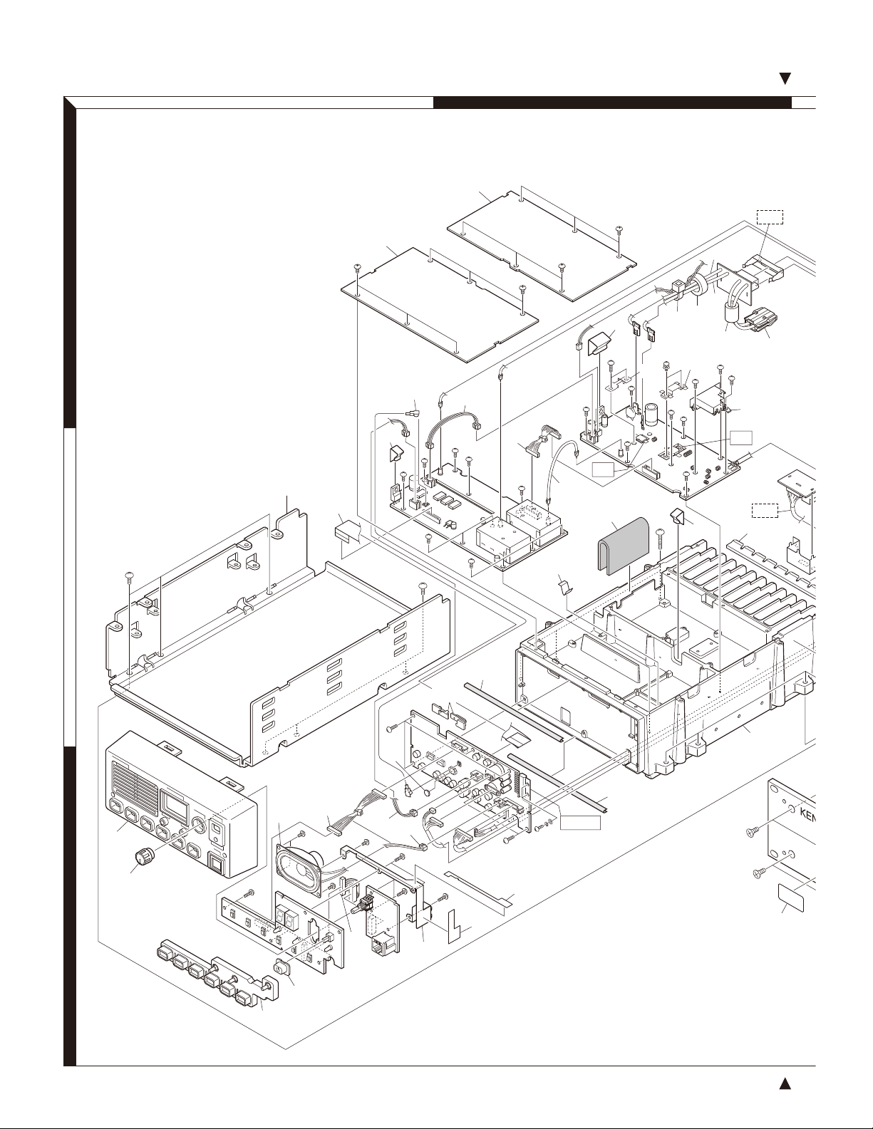
NXR-710
A : N09-2292-05
B M2.6 x 6 : N30-2606-48
C M4 x 6 : N30-4006-48
D M4 x 14 : N30-4014-48
E M4 x 20 : N30-4020-43
F M3 x 6 (F) : N32-3006-48
G M4 x 8 (F) : N32-4008-43
H M3 x 6 (Bi) : N35-3006-43
J M4 x 6 (Bi) : N35-4006-43
1
K M3 x 8 : N67-3008-48
L M2.6 x 8 : N80-2608-43
M M3 x 5 (Br-Tap) : N87-3005-43
N M3 x 6 (Br-Tap) : N87-3006-48
EXPLODED VIEW
3
2
Hx6
17
25
Nx6
BA
44
Nx2
Hx6
63
Kx2
67
76
41
20
21
75
X45
102
X45 (B/3)
13
Nx3
36
38
Nx10
24
Q4
Q3
39
26
52
X45 (A/3)
Dx3
38
X45
101
42
700
X57
28
Cx6
2
46
62x2
X53
701
80
46
Mx3
23
25
M
22
Nx6
Kx2
IC403
Gx6
78
1
70
3
Nx3
Nx2
49
Nx3
48
24
X54 (B/2)
X54 (A/2)
40
71
72
Parts with the exploded numbers larger than 700 are not supplied.
36
If a part reference number is listed in a box on the exploded view of the PCB, that part does not come with the PCB.
These parts must be ordered separately.
703
Page 37

EXPLODED VIEW
X
C D
NXR-710
X45
102
45 (B/3)
43
13
Fx2
Jx14
14
4
B
B
B
B
34
E
18
32
L
L
Bx2
E
29
Ax2
33
F
X45
45
(C/3)
B
47
B
01
6
X45
16
103
F
01
703
Dx3
707
706
11
Fx2
27
705
707
706
5
11
47x2
704
702
Parts with the exploded numbers larger than 700 are not supplied.
If a part reference number is listed in a box on the exploded view of the PCB, that part does not come with the PCB.
These parts must be ordered separately.
37
Page 38

NXR-710
56 Protection bag (H25-0762-04)
15 DC cord (E30-3427-35)
74 Line filter (L79-1419-05)
67 Band (J61-0307-05)
1
*1
54 Protection bag
(H25-0029-04)
60 Foot
(J02-0475-05) x 2
61 Foot (Rubber)
(J02-0492-04) x 2
66 Grommet
(J59-0302-05) x 2
C Pan head machine screw
(N30-4006-48) x 2
H Binding head machine screw
(N35-3006-43) x 5
PACKING
*1
*2
*3
713 Carton board
FE
50 Cushion (G13-1801-04) x 4
51 Cushion (G13-1802-04) x 4
55 Protection bag (H25-0747-04)
64 Mounting hardware (J21-8559-04)
710 Pamphlet
711 Pamphlet
10 Instruction manual
(B62-2199-00)
8 Front glass
(B10-2635-04)
9 Filter
(B11-1259-04)
57 Protection bag
(H25-2328-04)
712 Packing fixture
*2
69 Handle
(K01-0418-15)
*3
19 15P plug
2
(E31-3228-05)
32 Blade fuse
(F05-1537-05)
54 Protection bag
(H25-0029-04)
3
714 Protection bag
715 Packing fixture
716 Packing fixture
58 Item carton case
(H52-2334-02)
38
Parts with the exploded numbers larger than 700 are not supplied.
Page 39

ADJUSTMENT
Test Equipment Required for Alignment
Test Equipment Major Specifi cations
Frequency Range 136 to 174MHz
Modulation Frequency modulation and external modulation
1. Standard Signal Generator
(SSG)
2. Power Meter
3. Deviation Meter Frequency Range 136 to 174MHz
4. Digital Volt Meter (DVM)
5. Oscilloscope DC through 30MHz
6. High Sensitivity
Frequency Counter
7. Ammeter 15A or more
8. AF Volt Meter (AF V.M)
9. Audio Generator (AG)
10. Distortion Meter
11. Voltmeter
12. 4Ω Dummy Load Approx. 4Ω, 5W
Output –127dBm/0.1µV to greater than –20dBm/22.4mV
When performing the Frequency adjustment, the following accuracy is necessary.
• 0.003ppm
Use a standard oscillator for adjustments, if necessary.
Input Impedance 50
Operation Frequency 136 to 174MHz or more
Measurement Capability Vicinity of 100W
Measuring Range 1V to 20V DC
Input Impedance High input impedance for minimum circuit loading
Frequency Range 10Hz to 600MHz
Frequency Stability 0.2ppm or less
Frequency Range 50Hz to 10kHz
Voltage Range 3mV to 3V
Frequency Range 50Hz to 5kHz
Output 0 to 1V
Capability 3% or less at 1kHz
Input Level 50mV to 10Vrms
Measuring Range 10V to 1.5V DC or less
Input Impedance 50kΩ/V or greater
Ω
NXR-710
Test cable for microphone input (E30-3360-28)
GREEN
1
RED
2
BLACK
3
BLUE
4
SHIELD
5
WHITE
6
GRAY
7
YELLOW
8
PTT
MIC-E
MIC
HK
1
2
E
3
4
5
6
7
8
MIC connector (Front panel view)
81
1: NC
2: SB
3: GND
4: PTT/TXD
(PC serial data from transceiver)
5: MIC GND
6: MIC
7: HOOK/RXD
(PC serial data to transceiver)
8: NC
Tuning cable (E30-3383-05)
Adapter cable (E30-3383-05) is required for
injecting an audio if PC tuning is used.
See “PC Mode” section for the connection.
Lead wire +
Shield wire –
MIC
Flat cable (36-pin) about 256mm
To connect the Control unit (CN38) to the TX-RX unit
(CN800) while in servicing, you can use the 36-pin fl at cable,
E37-0979-05, which is available from the KENWOOD parts
center.
39
Page 40

NXR-710
ADJUSTMENT
Test Channel
No. RX TX
1 155.050000MHz 155.100000MHz
2 136.050000MHz 136.100000MHz
3 173.950000MHz 173.900000MHz
4 155.000000MHz 155.000000MHz
5 155.200000MHz 155.200000MHz
6 155.400000MHz 155.400000MHz
7~16 Blank Blank
Test Signaling (Analog)
No. RX (Decode Signaling) TX (Encode Signaling)
1 None None
2 None 100Hz Square Wave
3 QT 67.0Hz QT 67.0Hz
4 QT 151.4Hz QT 151.4Hz
5 QT 210.7Hz QT 210.7Hz
6 QT 254.1Hz QT 254.1Hz
7 DQT D023N DQT D023N
8 DQT D754I DQT D754I
9 None CWID Encode (ID: VVV)
10 None Single Tone
11
DTMF Decode (CODE: 159D)
12 None DTMF Encode (CODE: 9)
13 None Courtesy Tone
DTMF Encode (CODE: 159D)
Test Signaling (NXDN)
No. RX (Decode Signaling) TX (Encode Signaling)
1 RAN 1 RAN 1
2 RAN 1 PN 9
3 RAN 1 Maximum Deviation Pattern
• Signaling number 1 is used for link test.
• Signaling number 2 is used for TX modulation signal quality test. i.e, TX adjacent channel power, FSK error, Occupied bandwidth, Emission mask, etc.
• Signaling number 3 is used for TX deviation test. If the
modulation mode is very narrow, the modulation frequency is 600Hz. If the modulation mode is narrow, the
modulation frequency is 1200Hz.
Adjustment Points
40
2nd_Lo
450kHz
TX-RX UNIT
Component side
MOD
LDT
LDR
VOUT4
VOUT7
TX_CV
TX_AST
MO
ASWC
MB
MB_CV2
RX_AST
RX_CV
Page 41

ADJUSTMENT
Common Section
Measurement Adjustment
Item Condition
1. Setting 1) Connect the unit to a suitable power supply (13.6V).
2) Turn the power switch on after connecting a PC and FPU cable to the radio.
3) Start up the program for the adjustment.
Test-
equipment
Unit
Terminal
Unit Parts Method
NXR-710
Specifi cations / Remarks
2. RX Assist
voltage
Adjust
3. TX Assist
voltage
Adjust
FPU Test mode
1) Adjust Item: [Receive Assist]
2) Adjust Item: [A: Low],
[A: Center], [A: High],
[B: Low], [B: Center],
[B: High]
3) Adjust Item: [A: Low],
[A: Center], [A: High],
[B: Low], [B: Center],
[B: High]
FPU Test mode
1) Adjust Item: [Transmit Assist]
2) Adjust Item: [A: Low],
[A: Center], [A: High],
[B: Low], [B: Center],
[B: High]
Press [Transmit] button.
PC
3.0V ±0.1V
ADJ
[V] indicator on the PC window shows “VCO lock voltage”.
Change the adjustment value
to get “VCO lock voltage”
within the limit of the specifi ed voltage.
Press [Apply All] button to
store the adjustment value.
Confi rm the VCO lock voltage
approximately 3 seconds
after the adjustment value is
changed.
DVM TX-RX RX_CV Check 3.0V±0.1V
PC
3.0V ±0.1V
ADJ
[V] indicator on the PC window shows “VCO lock voltage”.
Change the adjustment value
to get “VCO lock voltage”
within the limit of the specifi ed voltage.
4. Sensitivity 1
Adjust
BPF Adjust
3) Adjust Item: [A: Low],
[A: Center], [A: High],
[B: Low], [B: Center],
[B: High]
Press [Transmit] button.
FPU Test mode
1) Adjust Item: [Sensitivity 1]
2) Adjust Item: [Low], [Low’],
[Center], [High’], [High]
Press [Apply All] button to
store the adjustment value.
Confi rm the VCO lock voltage
approximately 3 seconds
after the adjustment value is
changed.
DVM TX-RX TX_CV Check 3.0V±0.1V
PC
Write the value as
ADJ
followings (typical
value)
[Low] = 55
[Low’] = 70
[Center] = 85
[High’] = 110
[High] = 135
Press [Apply All] button to
store the adjustment value.
Variable-Capacitor Tune voltage is adjusted.
(Output voltage is adjustment
of BPF)
41
Page 42
NXR-710
Item Condition
5. Sensitivity 2
Adjust
BPF Adjust
FPU Test mode
1) Adjust Item: [Sensitivity 2]
2) Adjust Item: [Low], [Low’],
[Center], [High’], [High]
ADJUSTMENT
Measurement Adjustment
Test-
equipment
Unit
Terminal
Unit Parts Method
PC
ADJ
Write the value as
followings (typical
value)
[Low] = 65
[Low’] = 75
[Center] = 90
[High’] = 115
[High] = 145
Specifi cations / Remarks
Press [Apply All] button to
store the adjustment value.
Variable-Capacitor Tune voltage is adjusted.
(Output voltage is adjustment
of BPF)
6. AGC Target
Level adjust
7. AGC adjustment
[Analog Nar-
row]
8. AGC adjustment
[Analog
Wide]
9. AGC adjustment
[NXDN Very
Narrow]
10. Frequency
Adjust
FPU Test mode
1) Adjust Item: [AGC Target
Level Adjustment]
FPU Test mode
1) Adjust Item: [AGC Adjustment (Analog Narrow)]
2) Adjust Item: [Low], [Low’],
[Center], [High’], [High]
FPU Test mode
1) Adjust Item: [AGC Adjustment (Analog Wide)]
2) Adjust Item: [Low], [Low’],
[Center], [High’], [High]
FPU Test mode
1) Adjust Item: [AGC Adjustment (NXDN Very Narrow)]
2) Adjust Item: [Low], [Low’],
[Center], [High’], [High]
FPU Test mode
1) Adjust Item: [Frequency]
Connect the SSG to the RX
ANT.
CH: 1 (Analog Narrow)
SSG Output: –47dBm (1mV)
(CW (without modulation))
Caution:
Perform the frequency adjustment under the following condition.
• Temperature range of
+23°C to +27°C (+73.4°F to
+80.6°F).
(The temperature is displayed
on the frequency adjustment
screen of the KPG-129D.)
• Use an accuracy of 0.003ppm
for the SSG.
(Use a standard oscillator if
necessary.)
SSG Rear RX ANT PC
ADJ
Write the value as
followings (typical
value)
[AGC Target Level
Adjustment] = –18
Write the value as
followings (typical
value)
[Low] = 256
[Low’] = 256
[Center] = 256
[High’] = 256
[High] = 256
Press [Apply] button to store
the adjustment value.
Press [Apply All] button to
store the adjustment value.
Press [Start] button of [Auto
Tuning].
Press [Apply] Button to store
the adjustment value after the
automatic adjustment was
fi nished.
42
Page 43
Receiver Section
Item Condition
1. RD Output
level Adjust
[Analog
Wide]
FPU Test mode
1) Adjust Item: [RD Level (Analog Wide)]
Connect the SSG to the RX
ANT.
SSG setting
Frequency: Desired Frequency
Output: –53dBm (501µV)
MOD: 1.0kHz
DEV: ±3.0kHz
ADJUSTMENT
Measurement Adjustment
Test-
equipment
SSG
AF VTVM
Unit
Terminal
Rear RX ANT
Control
I/O Jack
RD (Pin
No.10)
Unit Parts Method
PC
ADJ
NXR-710
Specifi cations / Remarks
80mV ±5mV
Press [Apply] button to store
the adjustment value.
2. RD Output
level Adjust
[Analog Nar-
row]
3. RA Output
level Adjust
[Analog
Wide]
4. RA Output
level Adjust
[Analog Nr-
row]
FPU Test mode
1) Adjust Item: [RD Level (Analog Narrow)]
Connect the SSG to the RX
ANT.
SSG setting
Frequency: Desired Frequency
Output: –53dBm (501µV)
MOD: 1.0kHz
DEV: ±1.5kHz
FPU Test mode
1) Adjust Item: [RA Level (Ana-
log Wide)]
Connect the SSG to the RX
ANT.
SSG setting
Frequency: Desired Frequency
Output: –53dBm (501µV)
MOD: 1.0kHz
DEV: ±3.0kHz
FPU Test mode
1) Adjust Item: [RA Level (Ana-
log Narrow)]
Connect the SSG to the RX
ANT.
SSG setting
Frequency: Desired Frequency
Output: –53dBm (501µV)
MOD: 1.0kHz
DEV: ±1.5kHz
SSG
AF VTVM
Rear RX ANT
Control
I/O Jack
RA (Pin
No.11)
PC
400mV ±20mV
ADJ
Press [Apply] button to store
the adjustment value.
5. Open
Squelch
Adjust
[Analog
Wide]
FPU Test mode
1) Adjust Item: [Open Squelch
(Analog Wide)]
Connect the SSG to the RX
ANT.
SSG setting
Frequency: [Low], [Low’],
[Center], [High’], [High]
Output
: 12dB SINAD level –1dB
MOD: 1.0kHz
DEV: ±3.0kHz
2) SSG output: OFF Check The squelch shall be closed.
SSG
Audio
analyzer
Oscilloscope
Rear RX ANT PC
ADJ
Press [Apply] button to store
the adjustment value.
Note:
Write the fi xed value of “33”
when the adjustment value is
27 or less.
43
Page 44

NXR-710
Item Condition
6. Open
Squelch
Adjust
[Analog Nar-
row]
FPU Test mode
1) Adjust Item: [Open Squelch
(Analog Narrow)]
Connect the SSG to the RX
ANT.
SSG setting
Frequency: [Low], [Low’],
[Center], [High’], [High]
Output
: 12dB SINAD level –1dB
MOD: 1.0kHz
DEV: ±1.5kHz
2) SSG output: OFF Check The squelch shall be closed.
ADJUSTMENT
Measurement Adjustment
Test-
equipment
SSG
Audio
analyzer
Oscilloscope
Unit
Terminal
Rear RX ANT PC
Unit Parts Method
ADJ
Specifi cations / Remarks
Press [Apply] button to store
the adjustment value.
Note:
Write the fi xed value of “30”
when the adjustment value is
24 or less.
7. Open
Squelch
Adjust
[NXDN Very
Narrow]
8. Tight
Squelch
Adjust
[Analog
Wide]
FPU Test mode
1) Adjust Item: [Open Squelch
(NXDN Very Narrow)]
Connect the SSG to the RX
ANT.
SSG setting
Frequency: [Low], [Low’],
[Center], [High’], [High]
Output: 12dB SINAD level
of Analog Narrow –4dB
MOD: OFF
FPU Test mode
1) Adjust Item: [Tight Squelch
(Analog Wide)]
Connect the SSG to the RX
ANT.
SSG setting
Frequency: [Low], [Low’],
[Center], [High’], [High]
Output
: 12dB SINAD level +6dB
MOD: 1.0kHz
DEV: ±3.0kHz
2) SSG output: OFF Check The squelch shall be closed.
PC
ADJ
PC
ADJ
Press [Apply] button to store
the adjustment value.
Press [Apply] button to store
the adjustment value.
9. Tight
Squelch
Adjust
[Analog Nar-
row]
44
FPU Test mode
1) Adjust Item [Tight Squelch
(Analog Narrow)]
Connect the SSG to the RX
ANT.
SSG setting
Frequency: [Low], [Low’],
[Center], [High’], [High]
Output
: 12dB SINAD level +8dB
MOD: 1.0kHz
DEV: ±1.5kHz
2) SSG output: OFF Check The squelch shall be closed.
PC
ADJ
Press [Apply] button to store
the adjustment value.
Page 45

Item Condition
10. RSSI
Refarence
Adjust
[Analog
Wide]
FPU Test mode
1) Adjust Item [RSSI Ref (Analog
Wide)]
Connect the SSG to the RX
ANT.
SSG setting
Frequency: [Low], [Low’]
[Center], [High’], [High]
Output
: 12dB SINAD level –1dB
MOD: 1.0kHz
DEV: ±3.0kHz
ADJUSTMENT
Measurement Adjustment
Test-
equipment
SSG
Audio
analyzer
Unit
Terminal
Rear RX ANT PC
Unit Parts Method
ADJ
NXR-710
Specifi cations / Remarks
Press [Apply] button to store
the adjustment value.
11. RSSI
Refarence
Adjust
[Analog Nar-
row]
12. RSSI
Refarence
Adjust
[NXDN Very
Narrow]
13. Low RSSI
Adjust
[Analog
Wide]
FPU Test mode
1) Adjust Item [RSSI Ref (Analog
Narrow)]
Connect the SSG to the RX
ANT.
SSG setting
Frequency: [Low], [Low’]
[Center], [High’], [High]
Output
: 12dB SINAD level –1dB
MOD: 1.0kHz
DEV: ±1.5kHz
FPU Test mode
1) Adjust Item [RSSI Ref (NXDN
Very Narrow)]
Connect the SSG to the RX
ANT.
SSG setting
Frequency: [Low], [Low’]
[Center], [High’], [High]
Output
: 12dB SINAD level –1dB
MOD: OFF
FPU Test mode
1) Adjust Item [Low RSSI (Analog Wide)]
Connect the SSG to the RX
ANT.
SSG setting
Frequency: [Low], [Low’]
[Center], [High’], [High]
Output: –118dBm (0.28µV)
MOD: 1.0kHz
DEV: ±3.0kHz
SSG Rear RX ANT PC
ADJ
Press [Apply] button to store
the adjustment value.
14. Low RSSI
Adjust
[Analog Nar-
row]
FPU Test mode
1) Adjust Item [Low RSSI (Analog Narrow)]
Connect the SSG to the RX
ANT.
SSG setting
Frequency: [Low], [Low’]
[Center], [High’], [High]
Output: –118dBm (0.28µV)
MOD: 1.0kHz
DEV: ±1.5kHz
45
Page 46

NXR-710
Item Condition
15 .Low RSSI
Adjust
[NXDN Very
Narrow]
FPU Test mode
1) Adjust Item [Low RSSI (NXDN
Very Narrow)]
Connect the SSG to the RX
ANT.
SSG setting
Frequency: [Low], [Low’]
[Center], [High’], [High]
Output: –118dBm (0.28µV)
MOD: OFF
ADJUSTMENT
Measurement Adjustment
Test-
equipment
SSG Rear RX ANT PC
Unit
Terminal
Unit Parts Method
ADJ
Specifi cations / Remarks
Press [Apply] button to store
the adjustment value.
16. High RSSI
Adjust
[Analog
Wide]
17. High RSSI
Adjust
[Analog Nar-
row]
18. High RSSI
Adjust
[NXDN Very
Narrow]
FPU Test mode
1) Adjust Item [High RSSI (Analog Wide)]
Connect the SSG to the RX
ANT.
SSG setting
Frequency: [Low], [Low’]
[Center], [High’], [High]
Output: –70dBm (70.7µV)
MOD: 1.0kHz
DEV: ±3.0kHz
FPU Test mode
1) Adjust Item [High RSSI (Analog Narrow)]
Connect the SSG to the RX
ANT.
SSG setting
Frequency: [Low], [Low’]
[Center], [High’], [High]
Output: –70dBm (70.7µV)
MOD: 1.0kHz
DEV: ±1.5kHz
FPU Test mode
1) Adjust Item [High RSSI
(NXDN Very Narrow)]
Connect the SSG to the RX
ANT.
SSG setting
Frequency: [Low], [Low’]
[Center], [High’], [High]
Output: –70dBm (70.7µV)
MOD: OFF
SSG Rear RX ANT PC
ADJ
Press [Apply] button to store
the adjustment value.
19. Receiver
Sensitivity
Check
[Analog
Wide]
[Analog Narrow]
46
1) Connect the SSG to the RX
ANT.
SSG setting
Frequency: Desired Frequency
Output: –53dBm (501µV)
MOD = 1.0kHz
DEV: ±3.0kHz
AF: 0.45V/4
2) SSG setting
DEV: ±1.5kHz
Ω
SSG
Audio
analyzer
Oscilloscope
Rear RX ANT
TEST/
SPKR
Jack
pin 12
4Ω load
Check –115dBm (0.4µV) or Less
Page 47

Transmitter Section
Item Condition
1. High Transmit Power
Limit Adjust
FPU Test mode
1) Adjust Item: [High Transmit
Power Limit Adjust]
Frequency: [Low], [Low’],
[Center], [High’], [High]
Press [Transmit] button.
ADJUSTMENT
Measurement Adjustment
Test-
equipment
Power meter
Unit
Terminal
Rear TX ANT PC
Unit Parts Method
ADJ
NXR-710
Specifi cations / Remarks
53W±1.5W Press [Apply] button to store
the adjustment value.
2. High Transmit Power
Adjust
3. Low Transmit Power
Limit Adjust
4. Low Transmit Power
Adjust
5. Maximum
Deviation
Adjust
[NXDN Nar-
row]
FPU Test mode
1) Adjust Item: [High Transmit
Power ]
Frequency: [Low], [Low’],
[Center], [High’], [High]
Press [Transmit] button.
FPU Test mode
1) Adjust Item: [Low Transmit
Power Limit Adjust ]
Frequency: [Low], [Low’],
[Center], [High’], [High]
Press [Transmit] button.
FPU Test mode
1) Adjust Item: [High Transmit
Power Adjust ]
Frequency: [Low], [Low’],
[Center], [High’], [High]
Press [Transmit] button.
FPU Test mode
1) Adjust Item: [Maximum Deviation (NXDN Narrow)]
50W±0.5W
28W±1.5W
25W±0.5W
PC
Write the value as
ADJ
followings (typical
value)
[Maximum Deviation
(NXDN Narrow)] =
530
Press [Apply] button to store
the adjustment value.
6. Maximum
Deviation
Adjust
[NXDN Very
Narrow]
7. Maximum
Deviation
Adjust
[Analog
Wide]
8. Maximum
Deviation
Adjust
[Analog Nar-
row]
FPU Test mode
1) Adjust Item: [Maximum Deviation (NXDN Very Narrow)]
FPU Test mode
1) Adjust Item: [Maximum Deviation (Analog Wide)]
FPU Test mode
1) Adjust Item: [Maximum Deviation (Analog Narrow)]
Write the value as
followings (typical
value)
[Maximum Deviation
(NXDN Very Narrow)] = 530
Write the value as
followings (typical
value)
[Maximum Deviation
(Analog Wide)] =
530
Write the value as
followings (typical
value)
[Maximum Deviation
(Analog Narrow)] =
530
47
Page 48

NXR-710
Item Condition
9. Balance
Adjust
[20Hz Ad-
justment]
FPU Test mode
1) Adjust Item: [Balance]
Connect the Deviation Meter
to the TX ANT end via the ATT.
Deviation Meter setting
LPF: 3kHz
HPF: OFF
De-emphasis: OFF
2) Adjust Item: [A: Low],
[A: Center], [A: High],
[B: Low], [B: Center],
[B: High]
Press [Transmit] button.
20Hz is transmitted.
ADJUSTMENT
Measurement Adjustment
Test-
equipment
Deviation
meter
Oscilloscope
Unit
Terminal
Rear TX ANT PC
Unit Parts Method
ADJ
The Deviation of
20Hz frequency is
fi xed to 2.05kHz
Deviation.
Change the 2kHz
adjustment value to
become the same
deviation to 20Hz
within the specifi ed
range.
Specifi cations / Remarks
2kHz Tone deviation is within
±1.0% of 20Hz tone deviation.
Press [Apply All] button to
store the adjustment value
after all adjustment point was
adjusted.
[2.0kHz
Adjustment]
10. Standard
Modulation
Check
[Analog
Wide ]
FPU Test mode
1) Adjust Item: [Balance]
[2kHz Sine Wave] check box
is checked.
2) Adjust Item: [A: Low],
[A: Center], [A: High],
[B: Low], [B: Center],
[B: High]
Press [Transmit] button.
Check while transmitting
change to 2kHz.
1)
Connect the Deviation Meter
to the TX ANT end via the ATT.
Deviation Meter setting
LPF: 15kHz
HPF: OFF
De-emphasis: OFF
Detector: (p-p)/2
2) Connect the AG to the MIC
Terminal of MIC connector.
AG Frequency
: 1kHz (Sine Wave)
AG Output level: Adjust to
become the 3kHz Deviation.
Deviation
meter
Oscilloscope
AG
DVM
Rear
Front
TX ANT
MIC
Check 5.0mV±1.5mV
[Analog Narrow ]
48
1)
Connect the Deviation Meter
to the TX ANT end via the ATT.
Deviation Meter setting
LPF: 15kHz
HPF: OFF
De-emphasis: OFF
Detector: (p-p)/2
2) Connect the AG to the MIC
Terminal of MIC connector.
AG Frequency
: 1kHz (Sine Wave)
AG Output level: Adjust to
become the 1.5kHz Deviation.
Page 49
Item Condition
11. TD Deviation adjust
[Analog
Wide]
FPU Test mode
1) Adjust Item: [TD Deviation
(Analog Wide)]
Connect the Deviation Meter
to the TX ANT end via the ATT.
Deviation Meter setting
LPF: 3kHz, HPF: OFF
De-emphasis: OFF
2) Connect the AG to the TD
Terminal of Control I/O Jack.
AG Frequency
: 100Hz (Sine Wave)
AG Output level
: 0.5Vpp (177mVrms)
Press [Transmit] button.
ADJUSTMENT
Measurement Adjustment
Test-
equipment
Deviation
meter
Oscilloscope
AG
AF VTVM
Unit
Terminal
Rear TX ANT
Control
I/O Jack
TD (Pin
No.8)
Unit Parts Method
PC
ADJ
NXR-710
Specifi cations / Remarks
0.75kHz Deviation ±0.1kHz
Press [Apply] button to store
the adjustment value.
12. TD Deviation adjust
[Analog Nar-
row]
13. Transmit
Audio Input
(TA) adjust
[Analog
Wide]
FPU Test mode
1) Adjust Item: [TD Deviation
(Analog Narrow)]
Connect the Deviation Meter
to the TX ANT end via the ATT.
Deviation Meter setting
LPF: 3kHz, HPF: OFF
De-emphasis: OFF
2) Connect the AG to the TD
Terminal of Control I/O Jack.
AG Frequency
: 100Hz (Sine Wave)
AG Output level
: 0.5Vpp (177mVrms)
Press [Transmit] button.
FPU Test mode
1) Adjust Item: [Transmit Audio
Input (TA) (Analog Wide)]
Connect the Deviation Meter
to the TX ANT end via the ATT.
Deviation Meter setting
LPF: 15kHz, HPF: OFF
De-emphasis: OFF
2) Connect the AG to the TA
Terminal of Control I/O Jack.
AG Frequency
: 1kHz (Sine Wave)
AG Output level: 280mVrms
Press [Transmit] button.
Deviation
meter
Oscilloscope
AG
AF VTVM
Rear TX ANT
Control
I/O Jack
TA (Pin
No.9)
PC
3.0kHz Deviation ±0.1kHz
ADJ
Press [Apply] button to store
the adjustment value.
14. Transmit
Audio Input
(TA) adjust
[Analog Nar-
row]
FPU Test mode
1) Adjust Item: [Transmit Audio
Input (TA) (Analog Narrow)]
Connect the Deviation Meter
to the TX ANT end via the ATT.
Deviation Meter setting
LPF: 15kHz, HPF: OFF
De-emphasis: OFF
2) Connect the AG to the TA
Terminal of Control I/O Jack.
AG Frequency
: 1kHz (Sine Wave)
AG Output level: 280mVrms
Press [Transmit] button.
1.5kHz Deviation ±0.05kHz
Press [Apply] button to store
the adjustment value.
49
Page 50

NXR-710
Item Condition
15. QT Deviation adjust
[Analog
Wide]
FPU Test mode
1) Adjust Item: [QT Deviation
(Analog Wide)]
Connect the Deviation Meter
to the TX ANT end via the ATT.
Deviation Meter setting
LPF: 3kHz, HPF: OFF
De-emphasis: OFF
Detector: p-p/2
Press [Transmit] button.
ADJUSTMENT
Measurement Adjustment
Test-
equipment
Deviation
meter
Oscilloscope
Unit
Terminal
Rear TX ANT PC
Unit Parts Method
ADJ
Specifi cations / Remarks
0.75kHz Deviation ±0.05kHz
Press [Apply] button to store
the adjustment value.
16. QT Deviation adjust
[Analog Nar-
row]
17. DQT Deviation adjust
[Analog
Wide]
18. DQT Deviation adjust
[Analog Nar-
row]
FPU Test mode
1) Adjust Item: [QT Deviation
(Analog Narrow)]
Connect the Deviation Meter
to the TX ANT end via the ATT.
Deviation Meter setting
LPF: 3kHz, HPF: OFF
De-emphasis: OFF
Detector: p-p/2
Press [Transmit] button.
FPU Test mode
1) Adjust Item: [DQT Deviation
(Analog Wide)]
Connect the Deviation Meter
to the TX ANT end via the ATT.
Deviation Meter setting
LPF: 3kHz, HPF: OFF
De-emphasis: OFF
Detector: Peak hold
Press [Transmit] button.
FPU Test mode
1) Adjust Item: [DQT Deviation
(Analog Narrow)]
Connect the Deviation Meter
to the TX ANT end via the ATT.
Deviation Meter setting
LPF: 3kHz, HPF: OFF
De-emphasis: OFF
Detector: Peak hold
Press [Transmit] button.
0.35kHz Deviation ±0.05kHz
Press [Apply] button to store
the adjustment value.
0.75kHz Deviation ±0.05kHz
Press [Apply] button to store
the adjustment value.
0.35kHz Deviation ±0.05kHz
Press [Apply] button to store
the adjustment value.
19. DTMF
Deviation
adjust
[Analog
Wide]
20. DTMF
Deviation
adjust
[Analog Nar-
row]
50
FPU Test mode
1) Adjust Item: [DTMF Deviation (Analog Wide)]
Connect the Deviation Meter
to the TX ANT end via the ATT.
Deviation Meter setting
LPF: 15kHz, HPF: OFF
De-emphasis: OFF
Press [Transmit] button.
FPU Test mode
1) Adjust Item: [DTMF Deviation (Analog Narrow)]
Connect the Deviation Meter
to the TX ANT end via the ATT.
Deviation Meter setting
LPF: 15kHz, HPF: OFF
De-emphasis: OFF
Press [Transmit] button.
Deviation
meter
Oscilloscope
Rear TX ANT PC
ADJ
3.0kHz Deviation ±0.1kHz
Press [Apply] button to store
the adjustment value.
1.5kHz Deviation ±0.05kHz
Press [Apply] button to store
the adjustment value.
Page 51

Item Condition
21. Test Tone
Deviation
adjust
[Analog
Wide]
22. Test Tone
Deviation
adjust
[Analog Nar-
row]
23. CW ID
Deviation
adjust
[Analog
Wide]
24. CW ID
Deviation
adjust
[Analog Nar-
row]
25. Courtesy
Tone Deviation adjust
[Analog
Wide]
26. Courtesy
Tone Deviation adjust
[Analog Nar-
row]
FPU Test mode
1) Adjust Item: [Test Tone Deviation (Analog Wide)]
Connect the Deviation Meter
to the TX ANT end via the ATT.
Deviation Meter setting
LPF: 15kHz
HPF: OFF
De-emphasis: OFF
Press [Transmit] button.
FPU Test mode
1) Adjust Item: [Test Tone Deviation (Analog Narrow)]
Connect the Deviation Meter
to the TX ANT end via the ATT.
Deviation Meter setting
LPF: 15kHz
HPF: OFF
De-emphasis: OFF
Press [Transmit] button.
FPU Test mode
1) Adjust Item: [CW ID Deviation (Analog Wide)]
Connect the Deviation Meter
to the TX ANT end via the ATT.
Deviation Meter setting
LPF: 15kHz
HPF: OFF
De-emphasis: OFF
Press [Transmit] button.
FPU Test mode
1) Adjust Item: [CW ID Deviation (Analog Narrow)]
Connect the Deviation Meter
to the TX ANT end via the ATT.
Deviation Meter setting
LPF: 15kHz
HPF: OFF
De-emphasis: OFF
Press [Transmit] button.
FPU Test mode
1) Adjust Item: [Courtesy Tone
Deviation (Analog Wide)]
Connect the Deviation Meter
to the TX ANT end via the ATT.
Deviation Meter setting
LPF: 15kHz
HPF: OFF
De-emphasis: OFF
Press [Transmit] button.
FPU Test mode
1) Adjust Item: [Courtesy Tone
Deviation (Analog Narrow)]
Connect the Deviation Meter
to the TX ANT end via the ATT.
Deviation Meter setting
LPF: 15kHz
HPF: OFF
De-emphasis: OFF
Press [Transmit] button.
ADJUSTMENT
Measurement Adjustment
Test-
equipment
Deviation
meter
Oscilloscope
Unit
Terminal
Rear TX ANT PC
Unit Parts Method
ADJ
NXR-710
Specifi cations / Remarks
3.0kHz Deviation ±0.1kHz
Press [Apply] button to store
the adjustment value.
1.5kHz Deviation ±0.05kHz
Press [Apply] button to store
the adjustment value.
2.0kHz Deviation ±0.1kHz
Press [Apply] button to store
the adjustment value.
1.0kHz Deviation ±0.05kHz
Press [Apply] button to store
the adjustment value.
1.0kHz Deviation ±0.05kHz
Press [Apply] button to store
the adjustment value.
0.5kHz Deviation ±0.05kHz
Press [Apply] button to store
the adjustment value.
51
Page 52

NXR-710
Item Condition
27. Repeat
Gain adjust
[Analog
Wide]
28. Repeat
Gain adjust
[Analog Nar-
row]
FPU Test mode
1) Adjust Item: [Repeat Gain
(Analog Wide)]
Connect the Deviation Meter
to the TX ANT end via the ATT.
Deviation Meter setting
LPF: 15kHz
HPF: OFF
De-emphasis: OFF
2) Connect the SSG to the RX
ANT.
SSG setting
Frequency: Desired Frequency
Output: –53dBm (501µV)
MOD: 1.0kHz
DEV: ±1.0kHz
FPU Test mode
1) Adjust Item: [Repeat Gain
(Analog Narrow)]
Connect the Deviation Meter
to the TX ANT end via the ATT.
Deviation Meter setting
LPF: 15kHz
HPF: OFF
De-emphasis: OFF
2) Connect the SSG to the RX
ANT.
SSG setting
Frequency: Desired Frequency
Output: –53dBm (501µV)
MOD: 1.0kHz
DEV: ±1.0kHz
ADJUSTMENT
Measurement Adjustment
Test-
equipment
Deviation
meter
Oscilloscope
SSG
Unit
Terminal
Rear TX ANT
RX ANT
Unit Parts Method
PC
ADJ
Specifi cations / Remarks
1.0kHz Deviation ±0.1kHz
Press [Apply] button to store
the adjustment value.
Confi rmation and Alignment of Set-up to
Prevent Receiver Desensitization
1. Confi rmation of Duplexer alignment
The duplexer allows the Repeater to simultaneously transmit
and receive. To accomplish this, in the programmed receive frequency, the transmit frequency must be notched or suppressed
by 75dB or more. Additionally, on the programmed transmit frequency, the receive frequency must be notched or suppressed
by 75dB or more. The following figures are examples of Duplexer alignment using a spectrum analyzer.
Ref –10dBm
# Peak
Log
10dB/
V1 V2
V3 FC
AA
#Res BW 30kHz
52
Atten 5dB
TX
VBW 30kHz
75dB or more
RX
Span 20MHz
Sweep 50ms (401 pts)
2. Confi rmation of Repeater Desensitization
The following fi gure is a Test set-up for Repeater Desensiti-
zation.
After this Test set-up is completed, confirm the Repeater
Desensitization as mentioned below.
1) Disable the repeater mode.
2) Adjust the level of the RF generator until 12dB SINAD is
reached.
3) Increase the output of the RF generator by 1dB. (This increases the SINAD.)
4) Enable the repeater mode.
5) Read the SINAD level. It should not drop below 12dB
SINAD. If the SINAD is less then 12dB, check the tightness
of the connectors and the tuning of duplexer.
Attenuated
Duplexer
Repeater
port
RF signal
generator
50Ω
dummy
Page 53
TERMINAL FUNCTION
NXR-710
Final Unit (X45-3920-10) (A/3)
Pin No.
1 TX IN I TX driver input signal (Coaxial)
1 +B I Power supply input
1 GND - Ground
1 GND - Ground
2 +B O Power supply output
3 +B O Power supply output
1 GND - Ground
2 8TC I 8V power supply control
3 RAMP I RF power control voltage
4 ASWC I ANT switch control
5 FAN I FAN control
6 FDT O Coupler input voltage
7 TMP2 O Temperature of X45 Final unit
8 TMP1 O Temperature of X45 Final unit
9 PLIM I Power limit control
10 H/L I Power control
11 HWV2 O Hardware version detect
1 FAB O FAN power supply
2 FAG - FAN ground
Name I/O Function
CN1 (To X57-794 CN610)
CN201 (To X45-392 B/3 +B)
CN202 (To X45-392 B/3 GND)
CN203 (To X57-794 CN701)
CN204 (To X57-794 CN801)
CN205 (To FAN)
Final Unit (X45-3920-10) (B/3)
Pin No.
1 +B O Power supply output
1 GND - Ground
1 +B I Power supply input
1 GND - Ground
Name I/O Function
+B (To X45-392 A/3 CN201)
GND (To X45-392 A/3 CN202)
+B1 (To DC 13.6V)
GND (To DC 13.6V)
Final Unit (X45-3920-10) (C/3)
Pin No.
1 N_SYNC1_B I/O RS-485 differential signal 1-B
2 N_SYNC1_A I/O RS-485 differential signal 1-A
3 N_SYNC2_B I/O RS-485 differential signal 2-B
4 N_SYNC2_A I/O RS-485 differential signal 2-A
5 N_SYNC1_B I/O RS-485 differential signal 1-B
Name I/O Function
N_SYNC1, 2 (To X53-449 CN5)
Pin No.
6 N_SYNC1_A I/O RS-485 differential signal 1-A
7 N_SYNC2_B I/O RS-485 differential signal 2-B
8 N_SYNC2_A I/O RS-485 differential signal 2-A
1 N_SYNC1_B I/O RS-485 differential signal 1-B
2 N_SYNC1_A I/O RS-485 differential signal 1-A
3 N_SYNC2_B I/O RS-485 differential signal 2-B
4 N_SYNC2_A I/O RS-485 differential signal 2-A
Name I/O Function
J401, 402 (N_SYNC1, 2 jack)
Control Unit (X53-4490-10)
Pin No.
1 N_SYNC1_B I/O RS-485 differential signal 1-B
2 N_SYNC1_A I/O RS-485 differential signal 1-A
3 N_SYNC2_B I/O RS-485 differential signal 2-B
4 N_SYNC2_A I/O RS-485 differential signal 2-A
5 N_SYNC1_B I/O RS-485 differential signal 1-B
6 N_SYNC1_A I/O RS-485 differential signal 1-A
7 N_SYNC2_B I/O RS-485 differential signal 2-B
8 N_SYNC2_A I/O RS-485 differential signal 2-A
1 TMP1 I Temperature of X45 Final unit
2 TMP2 I Temperature of X45 Final unit
3 RAMP O RF power control voltage
4 FWD I RF power monitor voltage
5 TXASSIST O TX PLL assist voltage
6 RXASSIST O RX PLL assist voltage
7 TX_CV I TX VCO lock voltage
8 RX_CV I RX VCO lock voltage
9 GND - Ground
10 GND - Ground
11 TXVCOB O TX VCO B control signal
12 RXVCOA/B O RX VCO control signal to A or B
13 TXVCOA O TX VCO A control signal
14 /RXPCS_TR O RX PLL chip select signal
15 LDT I TX PLL lock detect signal
16 /16_8PCS O
17 LDR I RX PLL lock detect signal
18 /TXPCS O TX PLL chip select signal
19 SPSCLK0 O Serial clock
20 SPSD0 O Serial data
21 SBC O Switched +B control signal
22 GND - Ground
23 MOD O Audio signal for TX modulation
24 GND - Ground
25 RSSI I RSSI voltage
Name I/O Function
CN5 (To X45-392 C/3 )
CN38 (To X57-794 CN800)
Reference clock PLL chip select signal
53
Page 54
NXR-710
TERMINAL FUNCTION
Pin No.
26 AGC O Auto gain control voltage
27 33A O 3.3V voltage
28 /EWP O EEPROM write control signal
29 HWV1 I Hardware version signal
30 I2CCK O Serial clock
31 SPSCLK1 O Serial clock
32 I2CDA I/O Serial data
33 SPSD1 O Serial data
34 /IOCS I IO expander chip select signal
35 /EVCS O DA converter chip select signal
36 NC - No connection
IN IF_SIG I 450kHz IF signal
OUT GND - Ground
1 SB O Power supply input
2 SB O Power supply input
3 GND - Ground
4 NC - No connection
5 DAT O Serial data
6 PSW I Power switch signal
7 STB1 O Data latch signal
8 CLK O Serial clock
9 SOE O Output enable signal
10 TXD1 I/O MIC PTT, UART TX data
11 K1 I Key scan input
12 RXD1 I Hook detect signal, UART TX data
13 K2 I Key scan input
14 K3 I Key scan input
15 K4 O Key scan output
16 K5 O Key scan output
17 VLI I Speaker audio level control voltage
18 5C O 5V voltage
19 MIG - MIC ground
20 MIC I MIC signal
1 SB O Power supply output
2 SB O Power supply input
3 GND - Ground
4 GND - Ground
1 AO5 O Auxiliary output 5
2 AO4 O Auxiliary output 4
3 AO3 O Auxiliary output 3
4 SPO O Speaker AF output
5 SPO O Speaker AF output
Name I/O Function
CN39
CN40 (To X54-358 CN502)
CN41 (To TEST/SPKR 15pin Connector)
CN42 (To TEST/SPKR 15pin Connector)
Pin No.
6 AO2 O Auxiliary output 2
7 AO1 O Auxiliary output 1
8 SPI I Internal speaker AF input
9 RSI O RSSI voltage
10 RD O RX data output
11 SPG - Speaker ground
12 SPG - Speaker ground
1 SPO O Internal speaker AF output
2 SPG - Speaker ground
1 NC - No connection
2 NC - No connection
3 SPM_D25 I Speaker mute signal input
4 IO6_D25 I/O
5 RXG - RX signal ground for RA,RD
6 IO5_D25 I/O
7 RA_D25 O RX-Audio output (voice)
8 IO4_D25 I/O
9 RD_D25 O RX-DATA output (data or signaling)
10 IO3_D25 I/O
11 TA_D25 I TX audio input (voice)
12 IO2_D25 I/O
13 TD_D25 I TX-DATA input (data or signaling)
14 IO1_D25 I/O
15 DG - Control line ground
16 TXG - TX signal ground for TA,TD
17 AI3_D25 I Programmable function input 3
18
19 AI2_D25 I Programmable function input 2
20 SC_D25 O Squelch control output
21 AI1_D25 I Programmable function input 1
22 /EPTT_D25 I External PTT
23 TXD0_D25 O UART TX data
24
25 RXD0_D25 I UART RX data
26
27 NC (RSSI) No connection (RSSI)
28 NC - No connection
29 NC - No connection
30 NC - No connection
1 GND - Ground
2 +B I Power supply input
3 SB I Power supply input
Name I/O Function
CN43 (To INT SPKR )
CN44 (To Control I/O 25pin D-sub Connector)
Programmable function input/output 6
Programmable function input/output 5
Programmable function input/output 4
Programmable function input/output 3
Programmable function input/output 2
Programmable function input/output 1
BER_DATA_D25
EXT_MON_D25
BER_CLK_D25
O Bit error rate data
I External monitor signal
O Bit error rate clock
CN301 (To X57-794 CN700)
54
Page 55

TERMINAL FUNCTION
NXR-710
Display Unit (X54-3580-20) (A/2)
Pin No.
1 HK I Hook detection input/ RXD input
2 MIC I MIC signal input
3 MIG - MIC ground
4 PTT I/O PTT input/ TDX output
5 GND - Ground
6 NC - No connection
7SB O
8 NC - No connection
9 GND - Ground
10 5M O Common 5V output
11 VLI I Volume control input for AF signal
1 MIG - MIC ground
2 MIC O MIC signal output
3 VLI O Volume control output for AF signal
4 5C I Common 5V output
5 K4 I KEY input 4
6 K5 I KEY input 5
7 K2 O KEY input 2
8 K3 O KEY input 3
9 K1 O KEY input 1
10 HK/RXD O Hook detection output/ RXD input
11 SOE I Output enable for shift register
12 PTT/TXD I/O PTT output/ TDX input
13 STB1 I Strobe data for shift register
14 CLK I Clock data input
15 DAT I Serial data input
16 PSW O Power switch output
17 GND - Ground
18 NC - No connection
19 SB I
20 SB I
Name I/O Function
CN501 (To X54-358 B/2 CN601)
Power supply output after power switch
CN502 (To X53-449 CN40)
Power supply output after power switch
Power supply output after power switch
Display Unit (X54-3580-20) (B/2)
Pin No.
1 VLI O Volume control output for AF signal
2 5M I Common 5V input
3 GND - Ground
4 NC - No connection
5SB I
6 NC - No connection
7 GND - Ground
8 PTT I/O PTT output/ TDX input
Name I/O Function
CN601 (To X54-358 A/2 CN501)
Power supply output after power switch
Pin No.
9 MIG - MIC ground
10 MIC O MIC signal output
11 HK O Hook detection output/ RXD output
1 NC - No connection
2SB O
3 GND - Ground
4 PTT/TXD I/O PTT input/ TDX output
5 MIG - MIC ground
6 MIC I MIC signal input
7 HOOK/RXD I Hook detection input/ RXD input
8 NC - No connection
Name I/O Function
J601 (MIC jack)
Power supply output after power switch
TX-RX Unit (X57-7940-10)
Pin No.
1 RX_SIGNAL I Receive signal input (Coaxial)
1 GND - Ground
2 NC - No connection
3 80C_2 O 8V power supply
4 RXVCOA/B O VCO select
5 RX_CV I Control voltage input
6 NC - No connection
7 RXASSIST O Assist voltage output
1 VO I VCO input
2 GND - Ground
1 FIN O VCO output
2 SPSCLK0 O PLL clock output
3 /RXPCS_TR O PLL chip select output
4 SPSD0 O PLL data output
5 33C O 3.3V power supply
6 50C O 5V power supply
7 LDR I PLL lock detect input
8 REF O 19.2MHz reference clock output
1 REF IN I External reference input (Coaxial)
1 GND - Ground
2 TXVCOB O VCOB select
3 80C_1 O 8V power supply
4 TXVCOA O VCOA select
5 TX_CV I Control voltage input
6 MO O Modulation output
Name I/O Function
CN101 (To RX ANT)
CN202 (To X58-507 CN350)
CN203 (To X58-507 CN351)
CN204 (To X58-507 CN303)
CN500 (To Ext IN)
CN605 (To X58-508 CN350)
55
Page 56

NXR-710
TERMINAL FUNCTION
Pin No.
7 TXASSIST O Assist voltage output
1 VO I VCO input
2 GND - Ground
1 FIN O VCO output
2 SPSCLK0 O PLL clock output
3 /TXPCS O PLL chip select output
4 SPSD0 O PLL data output
5 33C O 3.3V power supply
6 50C O 5V power supply
7 LDT I PLL lock detect input
8 REF O 16.8MHz reference clock output
1 TX OUT O TX driver output signal (Coaxial)
1 GND - Ground
2 +B O Power supply output
3 SB O Power supply output
1 GND - Ground
2 +B I Power supply input
3 +B I Power supply input
1 NC - No connection
2 /EVCS I DA converter chip select signal
3 /IOCS O IO expander chip select signal
4 SPSD1 I Serial data
5 I2CDA I/O Serial data
6 SPSCLK1 I Serial clock
7 I2CCK I Serial clock
8 HWV1 O Hardware version signal
9 /EWP I EEPROM write control signal
10 33A I 3.3V voltage
11 AGC I Auto gain control voltage
12 RSSI O RSSI voltage
13 GND - Ground
14 MOD I Audio signal for TX modulation
15 GND - Ground
16 SBC I Switched +B control signal
17 SPSD0 I Serial data
18 SPSCLK0 I Serial clock
19 /TXPCS I TX PLL chip select signal
20 LDR O RX PLL lock detect signal
21 /16_8PCS I
22 LDT O TX PLL lock detect signal
Name I/O Function
CN608 (To X58-508 CN351)
CN609 (To X58-508 CN303)
CN610 (To X45-392 A/3 CN1)
CN700 (To X53-449 CN301)
CN701 (To X45-392 A/3 CN203)
CN800 (To X53-449 CN38)
Reference clock PLL chip select signal
Pin No.
23 /RXPCS_TR I RX PLL chip select signal
24 TXVCOA I TX VCO A control signal
25 RXVCOA/B I RX VCO control signal to A or B
26 TXVCOB I TX VCO B control signal
27 GND - Ground
28 GND - Ground
29 RX_CV O RX VCO lock voltage
30 TX_CV O TX VCO lock voltage
31 RXASSIST I RX PLL assist voltage
32 TXASSIST I TX PLL assist voltage
33 FWD O RF power monitor voltage
34 RAMP I RF power control voltage
35 TMP2 O Temperature of X45 Final unit
36 TMP1 O Temperature of X45 Final unit
1 HWV2 I Hardware version detect
2 H/L O Power control
3 PLIM O Power limit control
4 TMP1 I Temperature of X45 Final unit
5 TMP2 I Temperature of X45 Final unit
6 FDT I Coupler input voltage
7 FAN O FAN control
8 ASWC O ANT switch control
9 RAMP O RF power control voltage
10 8TC O 8V power supply control
11 GND - Ground
1 IF_SIG O 450kHz IF signal (Coaxial)
Name I/O Function
CN801 (To X45-392 A/3 CN204)
CN802 (To X53-449 CN39)
RX VCO/PLL Unit (X58-5070-10)
Pin No.
1 FIN I VCO input
2 SPSCLK0 I PLL clock input
3 /RXPCS_TR I PLL chip select input
4 SPSD0 I PLL data input
5 33C I 3.3V power supply
6 50C I 5V power supply
7 LDR O PLL Lock detect output
8 REF I 19.2MHz reference clock input
1 GND - Ground
2 NC - No connection
3 80C_2 I 8V power supply
4 RXVCOA/B I VCO select
5 RX_CV O Control voltage output
Name I/O Function
CN303 (To X57-794 CN204)
CN350 (To X57-794 CN202)
56
Page 57

TERMINAL FUNCTION
NXR-710
Pin No.
6 NC - No connection
7 RXASSIST I Assist voltage input
1 VO O VCO output
2 GND - Ground
Name I/O Function
CN351 (To X57-794 CN203)
TX VCO/PLL Unit (X58-5080-10)
Pin No.
1 FIN I VCO input
2 SPSCLK0 I PLL clock input
3 /TXPCS I PLL chip select input
4 SPSD0 I PLL data input
5 33C I 3.3V power supply
6 50C I 5V power supply
7 LDT O PLL lock detect output
8 REF I 16.8MHz reference clock input
1 GND - Ground
2 TXVCOB I VCOB select
3 80C_1 I 8V power supply
4 TXVCOA I VCOA select
5 TX_CV O Control voltage output
6 MO I Modulation input
7 TXASSIST I Assist voltage input
1 VO O VCO output
2 GND - Ground
Name I/O Function
CN303 (To X57-794 CN609)
CN350 (To X57-794 CN605)
CN351 (To X57-794 CN608)
CONTROL I/O 25 pin D-sub Connector
Pin
No.
Pin
Name
1NC -
2 RXD2 I
3 TXD2 O
4 AI1 I
5 AI2 I
6 AI3 I
7 DG - GND No Digital GND
8TD I
9TA I
10 RD O
11 RA O
I/O
Signal
Type
-
Digital
Digital
Digital
Digital
Digital
Analog
Analog
Analog
Analog
Modifi -
cation
Land short
No
No Asynchronous Send Data
No
No
No
No TX Data Input (signaling)
No TX Audio Input (voice)
No
No
Description/ Port Type
-
Asynchronous Receive
Data
Programmable Function
Input 1/ CMOS
Programmable Function
Input 2/ CMOS
Programmable Function
Input 3/ CMOS
RX Data Output (signaling)
Not Squelched
RX Audio Output (voice)
Squelched
Pin
No.
Pin
Name
12 RXG - GND No RX Signal GND
13 SPM I
BER_CLKODigital
14
15 EMON I
16 EPTT I
17 SC O
BER_DAT
18
19 TXG - GND No TX Siganl GND
20 IO1 I/O
21 IO2 I/O
22 IO3 I/O
23 IO4 I/O
24 IO5 I/O
25 IO6 I/O
I/O
O
Signal
Type
Digital
Digital
Digital
Digital
Digital
Digital
Digital
Digital
Digital
Digital
Digital
Modifi -
cation
No Speaker Mute/ CMOS
No for Bit Error Rate Clock
No External Monitor Switch
No External PTT Switch
No Squelch Control
No for Bit Error Rate Data
No
No
No
No
No
No
Description/ Port Type
Programmable Function I/O 1
Programmable Function I/O 2
Programmable Function I/O 3
Programmable Function I/O 4
Programmable Function I/O 5
Programmable Function I/O 6
TEST/SPKR 15 pin Connector
Pin
No.
Pin
Name
1SB -
2SB -
3NC - - No -
4 GND - GND No Digital GND
5 GND - GND No Digital GND
6 SPG - GND No Speaker GND
7RD O
8 RSSI O
9 SPI I
10 AO1 O
11 AO2 O
12 SPO O
13 AO3 O
14 AO4 O
15 AO5 O
I/O
Signal
Type
Power
Power
Analog
Analog
Analog
Digital
Digital
Analog
Digital
Digital
Digital
Modifi -
cation
No Power Supply
No Power Supply
No
No RSSI Output
No Internal Speaker Input
Default
$R203=47k
D23=delete
Default
$R202=47k
D29=delete
No External Speaker Output
Default
$R201=47k
D31=delete
Default
$R200=47k
D35=delete
Default
$R198=47k
D12=delete
Description/ Port Type
RX Data Output (signaling)
Not Squelched
Auxiliary Output 1
Open collector
Auxiliary Output 1
Open collector with PU
Auxiliary Output 2
Open collector
Auxiliary Output 2
Open collector with PU
Auxiliary Output 3
Open collector
Auxiliary Output 3
Open collector with PU
Auxiliary Output 4
Open collector
Auxiliary Output 4
Open collector with PU
Auxiliary Output 5
Open collector
Auxiliary Output 5
Open collector with PU
57
Page 58
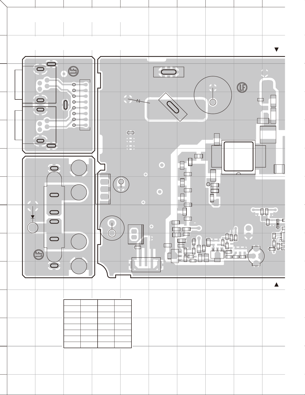
5
0
2
NXR-710 PC BOARD
1
FINAL UNIT (X45-3920-10)
2
Component side view (J79-0263-09)
JIHGFEDCBA
10
J79-0263-09
A/3
3
J401
N_SYNC2
4
J402
N_SYNC1
5
CN302
CN303
CN304
CN305
CN306
CN307
CN308
CN309
8
N_SYNC2_A
N_SYNC2_B
N_SYNC1_A
N_SYNC1_B
N_SYNC2_A
N_SYNC2_B
N_SYNC1_A
1
N_SYNC1_B
D202
R351
CN202
GND (BLACK)
CN201
+B (RED)
C223
+
C98
C37
F1
L8
C33
L9
J79-0263-09
C/3
L7
6
7
8
D301
CN301
9
J79-0263-09
GND
BLK
+B
RED
+B
RED
GND
BLK
IC203
+
OGI
C220
C19
C239
+
FAG12
CN205
FAB
C229
3+B
CN203
L4
C99
1
+B
GND
Q2BC
C27
L6
C26
L5
C25
C24
R24
R23
R21
R17R19
C17
R20
C18
E
C16
R18
C14
R15
R16
C12
R25
Vg
C28
R26
R27
R11
R8
C10
E
C
Q1
L3
R10
Q3GD
C34
R28
R29
C205
D201
C4
C6
R14
R6
R7
B
R9
R2
L19
C5
CN1
TXIN
C252
R201R202
R204
R
R2
1
IC
4
R2
C2
B/3
11
12
13
14
58
Ref. No. Address
IC201 9J
IC202 8L
IC203 7D
Q1 9H
Q2 9F
Q3 6I
Q4 5L
Ref. No. Address
D3 7Q
D4 9Q
D9 3Q
D10 8M
D201 8J
D202 4E
D301 8A
Page 59

JKLMNOPQRS
C205
L9
C252
F1
L8
D201
R201R202
C34
R205
18
45
R203
R204
C250
R208
IC201
C201
Vg
R207
R206
C251
R31
R210
R30
R32
R213
C253
C45
C206
R354
R215
18
IC202
45
C207
R218
R219
R217
Q4 DG
R237
R221
C210
R220
R33
D10
R225
R12
R39
11
HWV2
C51
TH201
H/L
C53
C216
PLIM
R226
TMP1
C60
C71
TMP2
CN204
C52
FDT
L10
FAN
ASWC
RAMP
PC BOARD NXR-710
FINAL UNIT (X45-3920-10)
Component side view (J79-0263-09)
D9
FWD
C94
C91 C92
D3
C66
R35
D4
L13
R40
8TC
1
GND
C54
ANT SW
R36
C57
L11
C68
C63
L12
R34
R38
C69
REV
L17
R41
C84
L18
L14
L16
C78 C89
GND
TX ANT
C88
L15
CN8
RX
1
2
3
4
5
6
7
C82
8
9
10
Component side
Layer 1
Layer 2
Layer 3
Layer 4
Foil side
11
12
13
59
14
Page 60

NXR-710 PC BOARD
1
FINAL UNIT (X45-3920-10)
2
3
4
Foil side view (J79-0263-09)
R43
C61
JIHGFEDCBA
C65
10
5
CN4
CN5
CN3CN2
6
D8
7
C80
D7
R44
8
C97
C75
R42
C249
C230
C231
C232
C233
C234
C235
C237
C244
C236
C247
9
11
12
13
14
Ref. No. Address
Q203 7O
Q204 6O
Q205 7O
Q206 6O
Q207 8O
D1 8L
D7 7A
D8 6A
D203 9O
60
Page 61

JKLMNOPQRS
C43
C44
C224
C225
C248
C23
Q203
C222
PC BOARD NXR-710
FINAL UNIT (X45-3920-10)
Foil side view (J79-0263-09)
J79-0263-09
A/3
J79-0263-09
C/3
Q204
S
R229
C221
S
D
G
R232
R233
G
S
D
G
G
S
Q206
D
D
R228
R230
Q205
R231
C218 C219
GND
BLK
+B
RED
C302
1
2
3
4
5
6
7
C21
C241
R235R236
D1
Q207
C7
C242
D203
C243
C245
C238
C246
C240
+B
RED
GND
BLK
C301
J79-0263-09
B/3
Component side
8
9
10
11
Layer 1
Layer 2
Layer 3
Layer 4
Foil side
12
61
13
14
Page 62
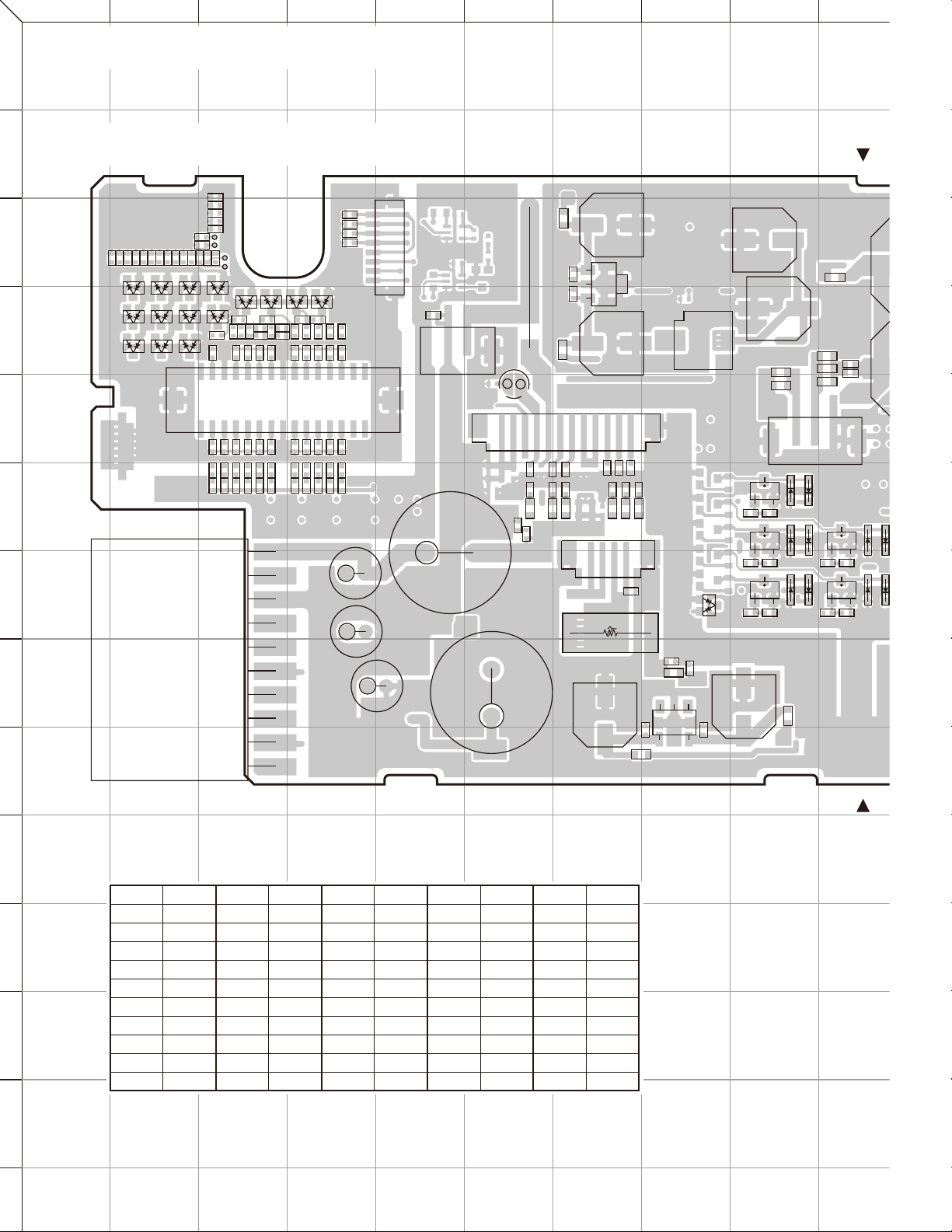
NXR-710 PC BOARD
1
CONTROL UNIT (X53-4490-10)
2
3
4
5
6
Component side view (J79-0277-09)
C162
C160
C157
C154
C152
CN32
C150
CN33
C147
CN34 CN35
C141
C142
C144
D20
D22 D26
C146
C149
C151
C153
D15 D16 D18
C145
C155
C159
C161
C164
C139
C143
D10
D14
D4
D9
D11
CN44
D6
D5
R167
R177 R180 R182
D7
R206
R220
R221
C192
C199
C203
12
RD_D25
RA_D25
RXG
SPM_D25
NC
IO3_D25
IO4_D25
IO5_D25
IO6_D25
NC
C195
C197
C201
C205
R219
R205
R207
R208
R168
R169
R171
R173
R218
R228
R227
R217
C213
C207
TD_D25
TA_D25
IO1_D25
IO2_D25
C210
C216
R216
R223
R174
R176
R225
R215
R230
R229
C220
C226
AI2_D25
AI3_D25
DG
BER_DATA_D25
SC_D25
TXG
C223
C229
R214
R224
R181
R178
R213
C232
AI1_D25
/EPTT_D25
C235
R212
R183
C9 1
C7
C10
C8
D8
R222
R211
C245
C239
NC(RSSI)
RXD0_D25
TXD0_D25
EXT_MON_D25
BER_CLK_D25
NC
C242
C249
R210
R209
R185
R187
CN5
8
29 30
NC
NC
N_SYNC1_B
N_SYNC1_A
N_SYNC2_B
N_SYNC2_A
N_SYNC2_B
N_SYNC2_A
N_SYNC1_B
N_SYNC1_A
C472
2
SPG
CN43
JIHGFEDCBA
L307
+
C322
C321
R281
SPO1
RSSI
CN37
CN36
SPG
SPG
RSI
SPI
RD
12
C212
C191
L9
C432
R430
C215
C189
L10
L306
CN42
AO1
C219
C187
L11
C314
AO2
SPO
O
IC302G
I
+
C312
AO5
AO4
AO3
SPO
1
C222
C225
C228
C180
C182
C185
L14
L15
L16
L305
R194
Q6
Q9
C311
R196
C310
L302
L301
+
R301
R302
+
+
D36
D32
L304
+
L314
L313
L303
3
1
GND
+B
SB
CN301
D13
D12
D31
Q10
10
11
12
+
C425
+
C430
7
C415
+
IC403
8
9
Ref. No. Address
IC25 8N
IC26 8N
IC27 8M
IC28 8M
IC302 3G
IC303 4M
IC304 4N
IC305 4R
IC306 8H
IC403 8B
110
Ref. No. Address
Q6 6I
Q7 7I
Q8 7J
Q9 6I
Q10 6J
Q302 5L
Q303 5L
D4 4B
D5 4C
D6 4C
Ref. No. Address
D7 4C
D8 4D
D9 4B
D10 4D
D11 4B
D12 6I
D13 6I
D14 4C
D15 4B
D16 4B
C422
+
Ref. No. Address
D18 4B
D20 4B
D22 4B
D23 7I
D24 7I
D26 4B
D28 7H
D29 7J
D30 7J
D31 6I
C404
+
Ref. No. Address
D32 6I
D35 6J
D36 6J
D37 7G
D302 4N
D304 5L
D305 5L
GND
4
CN41
GND
C327
+
D37
R254
SB
SB
1
C473
C330
L315
D28
C194
C209
L8
3
1
IC306
C331
4
5
R263 R267 R269
Q7
D24
R197 R199
C332
L316
+
D23
R204
Q8
D30
D29D35
R226
13
14
62
Page 63
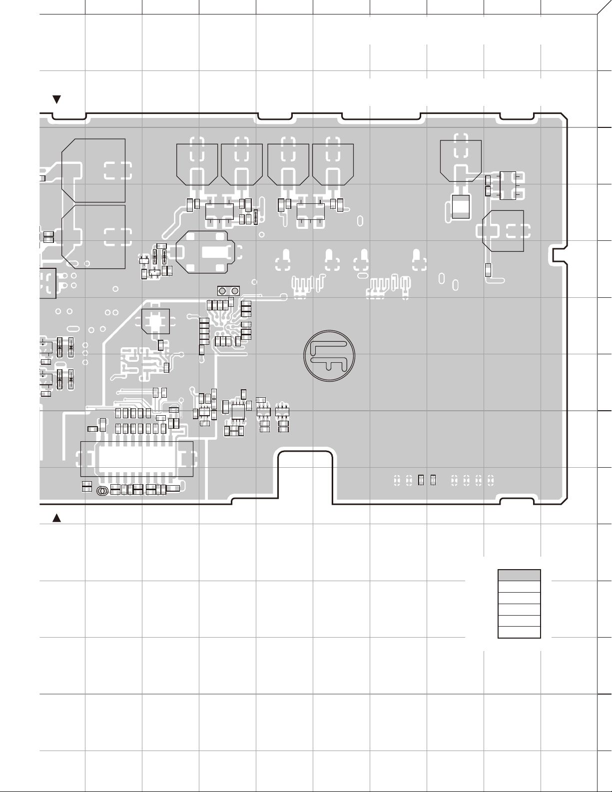
JKLMNOPQRS
PC BOARD NXR-710
1
CONTROL UNIT (X53-4490-10)
Component side view (J79-0277-09)
C316
+
R309
C320
C326
+
R324
4
5
C329
3
IC305
1
IC304
C315
C319
R310
4
3
C317
+
4
R301
R302
D36
C302
+
C301
Q302
S
D
R319
G
Q303
CN39
IF_SIG
R323
D305
R268
R321
++ ++
D304
R322
L308
C323C324
CN302
C98
C99
C101
C102
C103
R143
5
1
C121
C116
C115
IC303
CN25
C122
C129
4
3
C123
C128
CN24
C117
C318
C313
C120
L312
R308
/FLDM
C124
C125
C118
C119
C126
C127
D302
L309
C325C328
5
1
2
3
4
5
6
R269
R226
D30
D29D35
R265
R270
L317
C258
C259
12
DAT
GND
SB
PSW
NC
SB
PSW
R273
R271
R275
C196
CN45
CN46
R272
C256
STB1
CLK
C254
C193
R274
R276
C252
K1
SOE
CN40
RXD1
TXD1
C250
R277 R279
C190
C188
R278
K2
K3
C186
C184
C246
K4
K5
C243
C166
R266
R280
VLI
5C
C240
C466
R466
MIG
MIC
2019
L17
R467
IC28
R184
R179
3
4
C158
C148
15
R172
R175
C156
C140
R164
18
C138
R165
IC27
R163
45
R166
R170
R162
341634
C137
IC26
IC25
C135C136
C134
16
R503
R502
J79-0277-09
Component side
Layer 1
Layer 2
Layer 3
Layer 4
Layer 5
Layer 6
7
8
9
10
11
Foil side
63
12
13
14
Page 64

NXR-710 PC BOARD
1
CONTROL UNIT (X53-4490-10)
2
3
4
5
6
7
8
Foil side view (J79-0277-09)
R24
25
C20
L1
C11
48
L4
C260
C24
R65
C46
C29
R35
R62
C41
R73
R38
CN17: /INT4
CN13: FSDET
CN8: BER_DATA
CN12: /PCS_DSP
CN9: BER_CLK
CN10: BOOTM2
CN11: BOOTM1
R9
R3
R8
R4
R6
L6
R7
C50
IC12
34
15
R75
CP1
CN6
BOOTM3
R77
R66
R57
CP7 CP8
C42
C25
C26
C34
R14
R70
C44
C32
R5
R53
CN7
XF
R67
C33
R51
R71
CP2 CP3
C23
R64
C27
C45
R72
CP4CP5CP6
IC6
CN16
/INT5
R37
C43
R52
C28
C38
R36
R60
R32
C39
R59
R61
R63
C30
R58
R15
R68 R69
R34
R54
R55
R56
C47
CN15: /NMI
CN20: /DINT
CN21: /SYMTIM
CN19: /DWUP
IC3
CN14: CLKOUT
R29
R28
R27
R33
R40
R18
CN18: /INT3
CN4
L5
C40
R132
C92
C97
R135
X1
R30
C91
R119
JIHGFEDCBA
R44
R317
R318
C337
Q301
Q5
R186
R424
D401
D2
R101
R110
R113
R104
R111
R105
C73
R108
R107
45
18
IC15
C75
C74
R112
R74
C49C51
18
IC13
45
C52
C335
S
D
G
C423
R103
C72
R282
R83
R78
R50
R46
R45
R48
R49
R43
R47
14
C469
R426
TH1
R87
23
IC307
D303
C167
Q4
C65
C66
R190
C427
D1
C70
C333
R314
R191
R89
C69
R90
C67
R31
R315
R88
C68
C88
C87
120
10 11
C90
C89
120
IC18IC19
10 11
R154 R155
C131
R144
R161
CN31
R115
R156
R157
56
IC17
R123
R131
R133
R137
R160
CN30
HWV3
110
C95
C96
15
IC24
34
C130
C86
R128
R148
R153
C112
+
C81
C132
C133
R127
C108
C109
R510
R124
R508
R122
R118
R121
24
CN28
1
C31
IC9
C76
R114
C77
L18
IC16
34
16
C79
BSCAN1
CN27
BSCAN0
R95
R312
R102
116
R100
R99
R93
89
R92
R94
IC14
R82
L20
R138R141
R511
R81
D3
R159
ROUT
R509
CN26
SOFT_1
R116
R117
R79
C57
C61
C60
C56
LOUT
CN22
CN23
IC20
C114
C62C63
C85
CN29
C80
L7
14
+
C83
R130
R147
C110
R152
R146
C111
X2
8
C94
R145
C104
IC22
15 21
R320
C93
C82
R129
C84
R126
R142
17
28
22
C336
C471
23
14
IC308
R149
R150
R151
C334
L311
R316
R109
R85
C64
C470
R106
C58
R80
10
11
12
13
14
9
J79-0277-09
Ref. No. Address
IC3 4E
IC4 3O
IC5 4O
IC6 6C
IC7 3N
IC8 4N
IC9 6E
IC10 3M
IC11 4M
IC12 7B
Ref. No. Address
IC13 7J
IC14 8F
IC15 6I
IC16 8F
IC17 8H
IC18 4G
IC19 3G
IC20 6G
IC21 5K
IC22 4H
Ref. No. Address
IC23 5K
IC24 5H
IC301 3L
IC307 4J
IC308 5I
IC401 7N
IC402 7N
IC404 7L
IC405 5Q
IC406 5M
Ref. No. Address
IC407 7M
IC411 6M
IC412 5O
Q4 6J
Q5 4J
Q301 4I
Q401 7O
Q402 8O
Q403 8P
Q404 8N
Ref. No. Address
Q405 8Q
D1 6J
D2 5I
D3 4G
D301 4M
D303 4J
D401 5J
64
Page 65

JKLMNOPQRS
R44
R50
R46
R45
R48
R49
R43
R47
14
C469
R426
103
72
TH1
R87
83
78
23
IC307
D303
C167
Q4
C65
C66
R190
C427
D1
C70
C333
R314
R191
R89
C69
R90
C67
R315
R88
C68
R313
R457
R247
R249
R251
18
IC23
45
C100
110
IC21
5
C105
CN402
MOD
R412C408
R435
C418
R414
18
R415
C417
45
R236
R253
R245
R238
R244
L23
36
C107
C106
R233
35
NC
6
R252
C198
C306
R305
IC404
/EVCS
/IOCS
C200
C308
R250
C202
SPSD1
I2CDA
R304
IC301
110
C426
R248
C179
C206
R246
SPSCLK1
HWV1
I2CCK
R306
R307
R231
33A
/EWP
C211
56
AGC
C433
R243
RSSI
R303
R432
R242
C218
MOD
GND
C409
R439
GND
CN401
R241
C221
SBC
SPSD0
C224
C304
R413
R465
R462
C176
L22
R237
C227
SPSCLK0
LDR
/TXPCS
C230
C303
D301
R441
C424
18
R425
R422
C419
45
R464
C465
C463C464
R463
R461
C446
C445
CN404
SP
R234
R232
C175
R235
C241
R261
C247
LDT
TXVCOA
TXVCOB
GND
TX_CV
/RXPCS_TR
RXVCOA/B
/16_8PCS
RX_CV
GND
C244
C233
R262
C237
34
16
IC10
C36
34
16
IC11
C35
C429
IC406 IC411
C461
78
114
R451
R446
R445
C443
18
IC407
45
R257
R259
R260
C170
R255
C257
TXASSIST
RAMP
TMP1
1
RXASSIST
TMP2
FWD
2
R258
R256
R42
C455
C451
R450
CN38
C171
5
C22
C21
R437
C456
IC7
IC8
R452
C438
C436
C457
R444
C450
4
18
45
18
R41
C407
R409
R401
C403
IC401
16
34
R406R407
16
34
Q404
R25 R26
C18
R22
18
IC4 IC5
45
C19
R23
18
45
R460
R458
12
IC412
13
C459
C401
R403
IC402
C405
R410
S
R459
C460
Q401
R405
C402
Q402
D
PC BOARD NXR-710
CONTROL UNIT (X53-4490-10)
Foil side view (J79-0277-09)
R404
G
R402
R13
R12
C12C13 C14C15
R11
R10
C414
R416
C420
R421
R443
1
24
Q403
R423
C416
114
R417 R418
C421
78
R420
R408
C406
Q405
R419
R411
C410
C413
C412
IC405
MIC
R438
C434
R433
CN403
R436
C441
R442
C435C442
R431
C428
L2
L3
C462
1
2
3
4
5
6
7
8
9
Component side
Layer 1
Layer 2
Layer 3
Layer 4
Layer 5
Layer 6
10
11
Foil side
12
13
65
14
Page 66

1
NXR-710 PC BOARD
1
2
DISPLAY UNIT (X54-3580-20) Component side view (J79-0035-09)
3
VR601
4
5
JIHGFEDCBA
10
NC
HK
MIC
6
7
MIG
GND
NC
PTT
J601
SB
D503
TX
1
IC504
8
J79-0035-09 B/2
8
S501
PF1
S502
PF2
S503
PF3
S504
PF4
9
1346
Q512
11
12
13
14
66
Page 67

JKLMNOPQRS
D506
16
1
IC504 IC505
89
D507
16
1
89
PC BOARD NXR-710
DISPLAY UNIT (X54-3580-20) Component side view (J79-0035-09)
J79-0035-09 A/2
S507
POWER
D505
GRN RED
MAINDCBACK-
UP
1
2
3
4
5
6
03
X
D504
BUSY
7
8
S505
PF5
S506
PF6
Q514
16
43
Component side
Layer 1
Layer 2
Foil side
9
10
Ref. No. Address
IC504 6J
IC505 6L
11
Q512 10A
Q514 9P
D503 7J
D504 7M
D505 5R
12
D506 5J
D507 5L
67
13
14
Page 68

5
R524
5
0
X
NXR-710 PC BOARD
1
2
DISPLAY UNIT (X54-3580-20) Foil side view (J79-0035-09)
J79-0035-09 A/2
3
JIHGFEDCBA
4
5
BACKUP
6
R519
7
8
Component side
Layer 1
9
Layer 2
Foil side
RED
Q510
R543
Q507
6
1
34
MAIN DC
GRN
Q511
R544
R520
D513
R535
D514
R536
D510
R539
C520
D511
R540
R538
1
89
IC502
16
D509
R537
R534
C511
D508
+
D512
C524
C518
Q525
C525
O
R526
G
S
1
334
Q503
C526
R606
D
R541
R542
Q509
6
R518
I
IC507
G
R502R503
GND
GND
CN501
PTT
MIG
MIC
R517
4
1
6
Q506
Q504
BUSY
RED
11
VLI
5M
NC
SB
NC
HK
1
GRN
Q523
Q521
+
C501
CP504
446
3
1
6
34
1
CP503
C517
R505
VR501
Q502
+
R506
3
3
4
C523
C503
R507
Q501
1
61
6
Q524
Q522
I
IC506
R525
G
R508
Q518
Q517
61
1
6
O
D502
+
C502
34
34
C519
C522
+
D501
CP502
CP501
C521
C516
C505
C504
C507
Q508
C506
R516
R509
R510
1
3
4
6
Q519
1
3
4
6
Q516
RED
T
C
R
1
IC5
4
10
11
12
13
14
68
Ref. No. Address
IC501 9J
IC502 7D
IC503 9P
IC506 8I
IC507 8F
Q501 9I
Q502 9H
Q503 7F
Q504 7G
Q506 7G
Ref. No. Address
Q507 7B
Q508 8J
Q509 7F
Q510 6B
Q511 6C
Q513 9N
Q516 5J
Q517 5I
Q518 4I
Q519 4J
Ref. No. Address
Q521 5H
Q522 5I
Q523 4H
Q524 4I
Q525 6F
D501 9I
D502 9I
D508 7E
D509 8E
D510 6D
Ref. No. Address
D511 6D
D512 7E
D513 6C
D514 6D
D601 5R
D602 4R
D603 4R
Page 69

JKLMNOPQRS
R509
PC BOARD NXR-710
1
2
DISPLAY UNIT (X54-3580-20) Foil side view (J79-0035-09)
CN601
HK
MIC
MIG
PTT
11
C602
1
3
4
6
1
3
4
6
Q516 Q519
R601
GNDNCSBNCGND5MVLI
C606
C603
D603
C601
R604
D602
D601
R605
NC
MIC
PTT
SB
HK
MIG
GND
NC
1
C607
3
4
5
6
RED
R516
R510
GRN
TX
R524
C508
R511
1
8
IC501
45
R512
C509
R513
+
C510
R514
7
J79-0035-09 B/2
CN502
20
SB
NC
PSW
SB
GND
DAT
19
CLK
PTT/TXD
HK/RXD
STB1
SOEK1K2K4VLI
R529
K3K55C
MIC
MIG
12
R533
R523
C515
R530
Q513
1346
R531
C514
R532
R522
C512
16
1
IC503
C513
R521
9
8
8
9
10
11
69
12
13
14
Page 70

I
NXR-710 PC BOARD
1
TX-RX UNIT (X57-7940-10)
Component side view (J79-0265-09)
2
3
CN101
4
5
RX ANT
JIHGFEDCBA
R86
10
11
1
3+B
+B
R861
IC702
CN701
OGI
GND
R417
R418
+
CF400
C716
CN205
2nd_Lo
C411
C413
C410
C412
R406
C403
C406
C417
R421
R415
R416
R408
C408
R409 R410
34
IC400
15
R403
C400
CN700
1 GND
CN804
450kHz
+B
C439
R447
WIDE
CF401
C428
18
R431
SB
3
IC405 IC406
45
CN802
R702 R704
G
S
Q700
6
F700
7
+
C701
8
9
18
IC407
45
R442
R436
R433
S
G
D
Q701
D
C429
C438
CF402
NARROW
2
NC
1
R813 R814
/EVCS
/IOCS
18
IC408
45
18
45
R853
C831
R810
SPSD1
SPSCLK1
HWV1
I2CCK
I2CDA
R809
R811 R812
C437
R443
R437
R434
C430
CN806
MOD
IC806
45
18
R808
R806
RSSI
MOD
33A
CN800
AGC
GND
GND
/EWP
R807
SBC
CN803
L805
SPSCLK0
SPSD0
L806
LDR
/TXPCS
R803
CF403
VERY NARROW
CN600
LDT
LDR
TXVCOB
LDT
TXVCOA
/16_8PCS
RXVCOA/B
/RXPCS_TR
R801
R802
GND
GND
C818
C820
C814
TX_CV
RX_CV
RXASSIST
R444
R438
R435
15
IC801
R818
RAMP
TXASSIST
FWD
R850
R821
34
R800
TMP1
TMP2
35
R820
R819
36
CN810
VOUT4
I
C703 C705
C700
G
IC700
R700
O
CN814
VOUT7
R701
C702
R703
C704
+
C707
+
L700
C706
R707
C708
Q704
34
15
1
4
12
13
14
70
Ref. No. Address
IC203 9M
IC400 9D
IC405 8E
IC406 8F
IC407 6E
IC408 6F
Ref. No. Address
IC603 6O
IC604 6P
IC605 6M
IC606 5M
IC608 5M
IC700 10I
Ref. No. Address
IC701 11J
IC702 11B
IC703 10K
IC801 9H
IC806 9F
Q700 10E
Ref. No. Address
Q701 10E
Q704 11J
Q705 10K
Q706 9K
Page 71

JKLMNOPQRS
C707
R860
PC BOARD NXR-710
1
TX-RX UNIT (X57-7940-10)
Component side view (J79-0265-09)
CN801
H/L
PLIM
TMP1
TMP2
FDT
FAN
ASWC
RAMP
8TC
1 HWV2
C656
+
C661
R660
R657
R661
R665
18
IC608
45
C176
R100
CN603
MO
+
C323
C649
R642
R641
R645
34
R643
CN500
EXT IN
IC606
34
IC605
15
15
R658
R634
C645
C660
CN606
TX_CV
R659
C652
R648
CN604
TX_AST
C638
R637
GND
TXVCOB
80C_1
TXVCOA
TX_CV
MO
TXASSIST
R638
GND
11
CN601
MB
CN805
ASWC
R616
R617
C628
IC603
C631
R624
15
34
CN610
A2: TX VCO/PLL UNIT
(X58-5080-10)
C632C635
C644
CN602
MB_CV2
R636
R629
GND
VO
FIN
SPSCLK0
/TXPCS
SPSD0
33C
50C
LDT
REF
34
15
R633
C642
IC604
CN201
RX_AST
2
3
4
5
6
7
REF
LDT
50C
33C
C246
34
15
IC203
Q706
R710
S
D
G
R708
+
Q704
34
15
L700
18
C706
45
R707
C708
IC701
+
G
Q705
C719
R712
D
C712
S
C710
C725
C726
15
IC703
R709
34
C720
R715 R717
C721
C714
C724
C715 C717
R711
R713R714
R716
L701
L702
C729
L212
R250R251
SPSD0
/RXPCS_TR
SPSCLK0
FIN
GND
A1: RX VCO/PLL UNIT
(X58-5070-10)
VO
C210
+
RXASSIST
NC
RX_CV
RXVCOA/B
80C_2
NC
GND
CN200
RX_CV
J79-0265-09
8
9
10
11
12
Component side
Layer 1
Layer 2
Layer 3
Layer 4
13
Foil side
71
14
Page 72
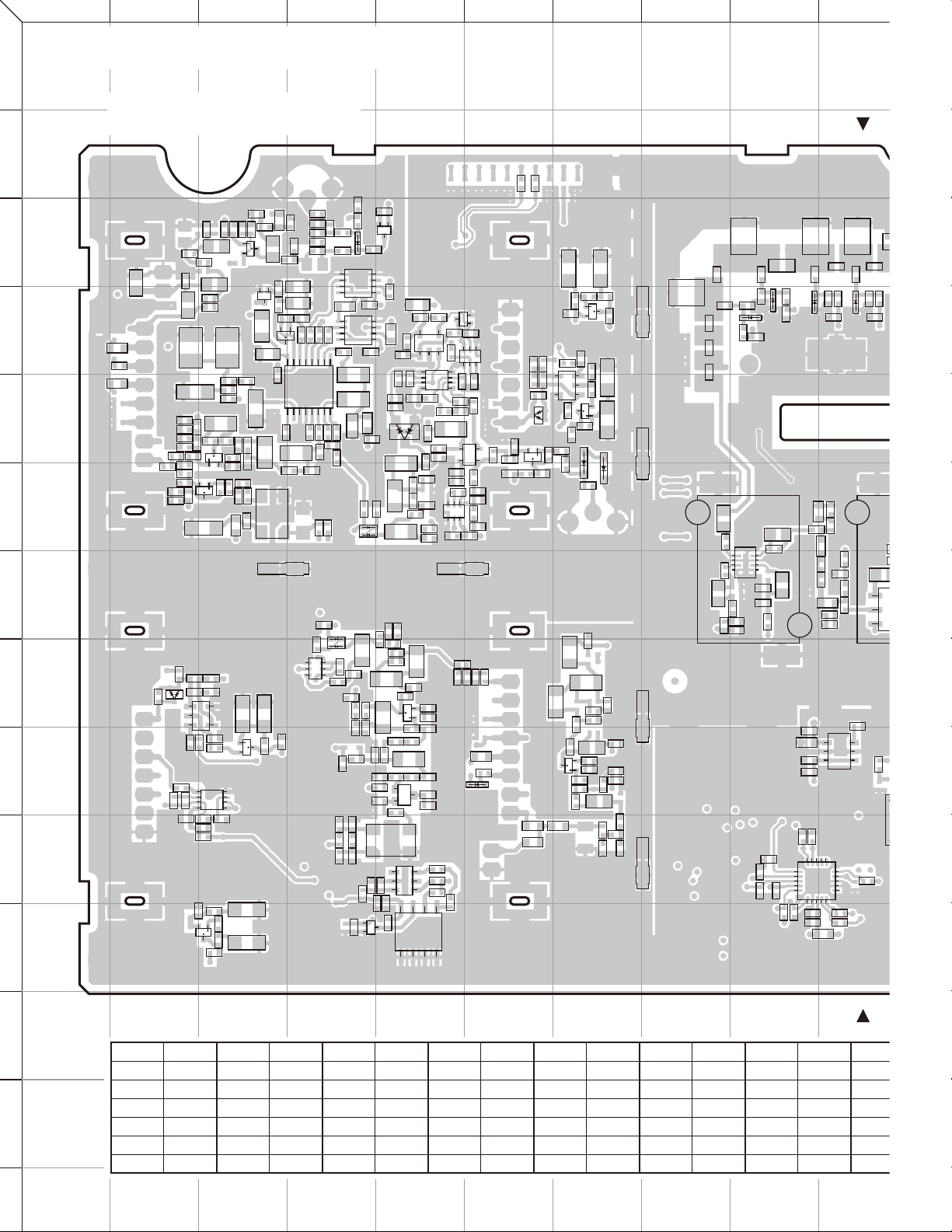
Q
C
124
NXR-710 PC BOARD
o
4
5
6
7
2
3
1
TX-RX UNIT (X57-7940-10)
Foil side view (J79-0265-09)
2
C673
L617
R671
C684
C672
R670
C671
R668
C680
C664
R666
L608
C618
R621
R622
R627
C643
15
IC201
3
C204
R205
R200
R206
R208
C211
Q201
L609
L607
+
R618
R212
4
C203
R203
IC200
C209
R214
L606
Q602
Q603
+
R207
R615
R620
C623
R630
45
18
R215 R216
+
R619
C629
R669
Q606
Q600
C621
R613R614
+
C614
C622
C619 C620
R632
C636
R631
C641
C639
R635
C201
++
Q200
+
C208
+
C207
S
L600
C606
G
D
Q601
L605
C200
R201
L610
R607
C605
X600
C674
R604R605
C247
R689
C600
C601
C604
R606
IC602
116
R609
L604
C615C616
10
11
3
4
SPSCLK0
L615
/TXPCS
R663
L616
SPSD0
5
6
L618
FIN
33C
50C
LDT
REF
GND
VO
C663
R626
C637
C634
C667
C625
C624
C627
R623
R625
C633
R628
C662
+
C626
C630
7
C206
NC
80C_2
NC
GND
R213
R209
D200
R202
R204
C205
R210 R211
C202
8
RXASSIST
RX_CV
9
RXVCOA/B
J79-0265-09
C683
R682
R680
R690
R672
R685
C612
16
34
Q506
C687
R687
C679
R681
C685
IC601
C602
L614
IC600
R683
R684
R608
L601
L603
89
C607
C610
C611
C613
R611
R612
R610
R639
R640
D504
R552
C548
D505
R535
C543
R541
C533
R533
C538
R523
C551
C504
C505
R507
R501
C502
R502
R822
Q800
D601
R686
45
18
45
18
C603
C608
C550
L507
R537
C536
L803
G
S
L602
C519
R514
R509
D
C686
C547
C524
C817
C819
S
C545
L505
X500
C815
G
D
R527
C531
D503
R545
C546
R543
L504
C530
R525
R515
C508
C821
Q607
R602
C542
C541
R540
L613
R539
IC501
34
15
R534
IC500
R528
R529
C532
R521
R524
C515
C522
C523
L502
C534
C526
C525C528
L503
C529
C544
Q500
R551
L508
C549
R547
R548
L506
C539
C537
C535
R538
Q504
R531 R532
R530
L501
C517
C521
Q502
D
S
C514
G
R518
R817
16
IC800
R816
34
R825
R826
IC802
45
18
R536
45
18
L500
C510
Q505
R520
C520
C518
R519
R500
16
CN812CN813
R824
R542
R546
S
D
G
C540
D
SG
34
R511
R549
3
4
R522
Q503
R550
D801
G
C512
R510
C511
L213
16
R544
R516
R512 R513
R220
R217
C212
VO
GND
GND
TXVCOB
80C_1
Q507
TXVCOA
TX_CV
MO
TXASSIST
C507
C509
C503
REF
LDT
50C
33C
SPSD0
/RXPCS_TR
SPSCLK0
FIN
R506
R504
R815
R248
R247
R654
C657
R656
D600
Q501
C506
R851
R655
R653
C654
++
C655
C658
Q605
R647
C651
34
C650
IC607
R646
15
R652
R644
C688
R503
R505
C501
D500
C500
C245
L210
L209
L208
C241
C239
R238
L207
C237
Q203
C235
R237
R234
R233
L211
R224
R249
C653
R650R651
Q604
+
+
C236
C231
C227
R235
R231
C224
R230
R649
C648
C647
D501
C243
C229
R232
CN807CN808
CN809CN811
L100
C101
C160
R101
C105
C102
L312
L308
R244
C103
C332
18
45
C331
C322
R245
R243
L101
D100
C104
R105
IC300
C339
C325
C107C108
R849
R847 R848
L315
C333
R320
L102
D101
R846
R106
C106
L309
R845
C727
11
15
R844
D103
C334
C728
C722
C718
R843
10
IC805
16 20
C827
C828
L103
C112
R842
L801
L316
L313
C335
C338
L320
C346
R310
6
C115
C114
4
C113
C336
R332
C349
IC704
5
1
R838
R841
R109
D104
R318
R312 R313
C723
3
16
JIHGFEDCBA
L104
C117
R840
C161
C118
C116
L804
B
C121
R110
E
E
R855
12
13
14
72
Ref. No. Address
IC100 4P
IC101 4O
IC200 9C
IC201 8C
IC300 7I
IC401 7Q
Ref. No. Address
IC402 8P
IC403 7P
IC404 8O
IC409 7Q
IC500 5E
IC501 4E
Ref. No. Address
IC600 4D
IC601 3D
IC602 5D
IC607 5G
IC704 9J
IC800 10E
Ref. No. Address
IC802 11E
IC803 10L
IC804 10K
IC805 10I
Q100 4Q
Q101 3K
Ref. No. Address
Q200 9C
Q201 11C
Q202 6P
Q203 9G
Q300 7O
Q301 7J
Ref. No. Address
Q500 6E
Q501 5F
Q502 9E
Q503 5F
Q504 8E
Q505 4E
Ref. No. Address
Q506 8D
Q507 4F
Q600 4C
Q601 4C
Q602 5C
Q603 6C
Ref. N
Q60
Q60
Q60
Q60
Q70
Q70
Page 73

JKLMNOPQRS
R109
PC BOARD NXR-710
1
TX-RX UNIT (X57-7940-10)
Foil side view (J79-0265-09)
2
CN102
C129
C130
CN106
GND
R125
GND
XF300
R128
R129
C134
D105
R323
L111
C137
C318
C135C136
C138
R133
C139
R134
L112
C140
C141
C356
L113
D106
C305
C306
D107
L302
R301
R305
C304
C144C145
C146
C302
E
G
R306
R135
C301
CG
R304
L114
C337
C147
C148
L300
R303
R300
Q300
C303
R136
C350
R429
C150
L301
C300
R302
R427 R428
L115
C149
C347
L317
34
C151
D108
C142
C131
R126
IC404
C427
34
C832
15
C152
IC101
C423C424
R114
R132
R223
C425
R425R426
C426
C154
L116
R118 R119
R111 R112
C109
R228
IC403
L203
R400
C119
Q202
C221
C419
R404
C402
R113
R229
IC402
IC100
C416
R422
R413
C405
51
43
C418
34
15
R453
15
R130
R131
C223
R227
C222
R225
C220
C219
C421
114
78
C422
L205
R236
R412
L117
C225
C233
L206
C414
C226
C228
C230
C234
R420
C415
C156
+
C110
Q100
R448
R450
R402
18
IC409
45
45
IC401
C407
R107
18
R405
L118
R449
C440
R411
C404
C401
R451
R452
R407
R401
C158
L119
3
4
5
6
7
8
9
R115
C127
L108
L104
C121
R137
C124
C161
15
C117
C120
R110
C118
D104
C116
4
R315
C341
R318
349
L804
E
R312 R313
Q301EBC
C723
3
704
1
R855
C344
C345
C343
L107
R314
R311
C342
C125
R117
R316
R856
L303
Q101
L105
C122
BC
L106
R122
E
R121
L109
E
R120
C123
C326
L310
C329
C825
IC804
124
R840
L800
C826
838
841
R833
s Ref. No. Address
Q604 5G
Q605 4G
Q606 3C
Q607 3E
Q702 10P
Q703 10Q
12 13
R837
R834
R835
Ref. No. Address
Q800 11D
D100 4I
D101 4I
D103 4I
D104 4J
D105 4M
R829
C823
R827
R830
R828
C822
IC803
R831
45
18
D106 4N
D107 4N
D108 4O
D200 8B
D500 6G
D501 6G
R832
Ref. No. Address
Ref. No. Address
D503 5E
D504 6D
D505 8D
D600 5F
D601 3D
D801 9F
S
D
Q702
G
R705R706
Q703
C713
C709
C711
10
11
12
Component side
Layer 1
Layer 2
Layer 3
Layer 4
13
Foil side
73
14
Page 74
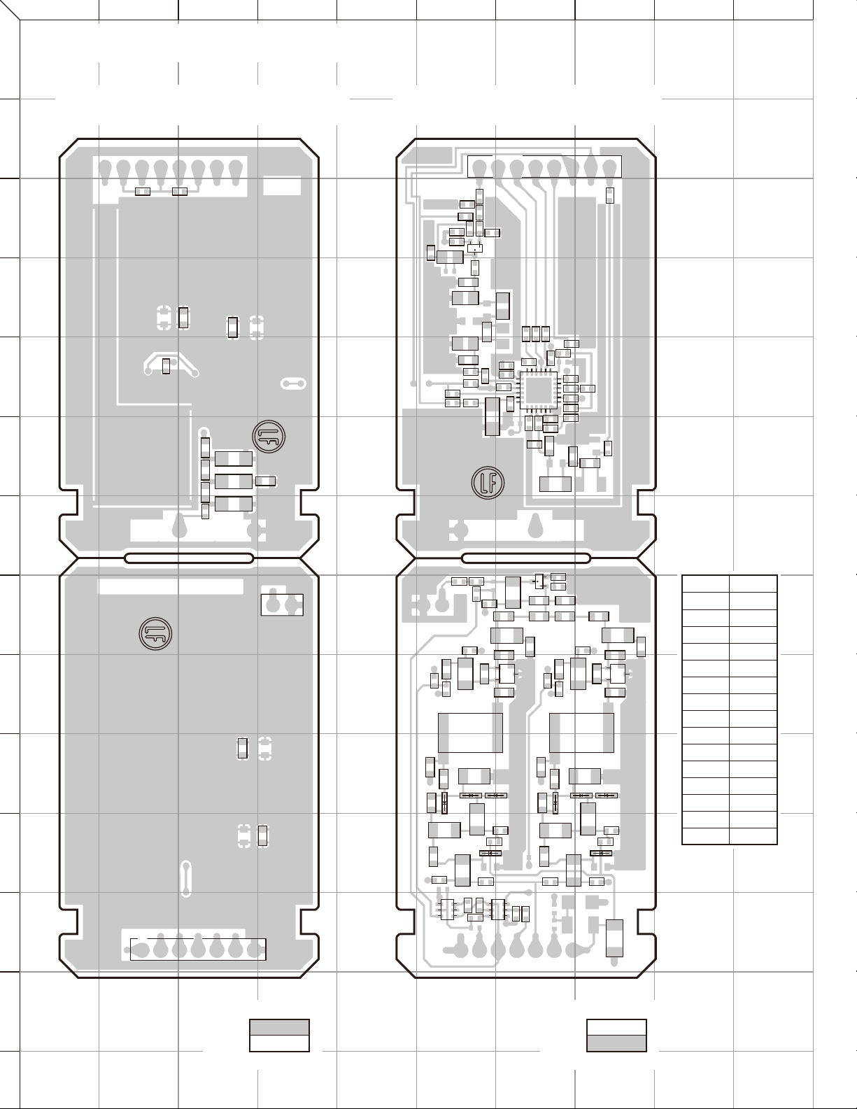
NXR-710 PC BOARD
1
JIHGFEDCBA
RX VCO/PLL UNIT (X58-5070-10)
Component side view (J79-0267-09)
2
LDT
REF
50C
R313 R314
3
4
5
6
33C
C322
SPSD0
R325
/RXPCS_TR
SPSCLK0
+
+
L300R301R303R305
+
R331
C307
C303
C300
FIN
R302
RX VCO/PLL UNIT (X58-5070-10)
Foil side view (J79-0267-09)
50C
C304
L312
R327
LDT
8
REF
R333
C333
C329
L315
R310
L310
R319
C331
R323
R312
C328
L314
L307
C312
R307
C326
R308
R320
C330
FIN1
R322R324
C332
R321
Q300
C323
C311
SPSCLK0
L309
C318
C317
C316
+
C314
/RXPCS_TR
R315
C324
1
C315
6
712
C308
R304
CN303
SPSD0
R316
IC300
C309
R317
C313
1924
C310
R306
C306
33C
18
13
L303
L313
C335
C320
R311
C321
L306
L305
10
11
12
7
J79-0267-09 A/2
J79-0267-09 B/2
8
9
CV GND CVGND
1
VO
CN351
2
GND
GND
C359
R372
VO
R362
C361
L361
C378
R367
C376
C371
J79-0267-09 A/2
C377
L364
Q354
R370
R368 R369
R365R366
C374C375
L362L363
R364
S
G
D
C358
R361
C360
C366C367
L360
C370
R363
C372C373
S
Q352Q353
G
D
C368C369
Ref. No. Address
IC300 5G
Q300 3F
Q350 12G
Q351 12F
Q352 9H
Q353 9G
Q354 8G
D352 11H
RXASSIST
NC
7
RX_CV
RXVCOA/B
CN350
80C_2
C364
C380
C354
R357
C362
L352L353
NC
D355
L350
RXASSIST
L358L359
L356L357
D358 D359D360 D361
L354
C356C357
L365L366
D352D353
C353
C379
R377
C365
C363
D357
C381
L355
R374
C355
L351
C352
GND 1
NC
16
3
Q351
GND
R351
R352
R358
R350
NC
Q350
80C_2
34
R354
164
RXVCOA/B
R379
RX_CV
J79-0267-09 B/2
D353 11F
D355 10G
D357 10F
D358 10H
D359 10H
D360 10F
D361 10G
13
14
74
Component side
Layer 1
Layer 2
Foil side
Component side
Layer 1
Layer 2
Foil side
Page 75

ABCDE FGH I J
TX VCO/PLL UNIT (X58-5080-10)
Component side view (J79-0268-09)
SPSCLK0
/TXPCS
50C
R313
33C
C322
SPSD0
R325
L300R301R303R305
FIN
R331
+
C307
+
R302
C303
+
C300
REF
LDT
PC BOARD NXR-710
TX VCO/PLL UNIT (X58-5080-10)
Foil side view (J79-0268-09)
50C
C304
L312
R327
LDT
8
REF
R333
C333
C329
L315
R318
R310
L310
R319
C331
R323
R312
C328
L314
L307
C312
R320
R307
C326
R308
FIN1
R322R324
C332
C330
R321
Q300
C323
C311
SPSCLK0
L309
C318
C317
C316
+
C314
/TXPCS
R315
C324
1
C315
6
712
C308
CN303
SPSD0
R316
IC300
C309
R317
C313
1924
C310
R306
C306
L303
33C
18
13
L313
C335
C320
R311
C321
L306
L305
1
2
3
4
5
6
J79-0268-09 A/2
J79-0268-09 B/2
TXASSIST
7
CV GND CVGND
1
2
MO
TX_CV
TXVCOA
CN350
80C_1
R377
TXCVOB
GND
VO
CN351
R374
GND 1
GND
J79-0268-09 B/2
C355
VO
R373
Q351
R371
R372
C378
L364
R367
C376
Q353
C363
D357
16
3
C367
D
G
L351
GND
R364
C369
C373
S
L355
D353
C384 C382
R358
R350
R351
34
R354
164
Q350
R353
TXCVOB
80C_1
TXVCOA
Q354
R368 R369
R365R366
R361R362
C358C359
C360C361
C354
R357
R379
TX_CV
C377
R370
C362
L352L353
R355R356
MO
Q352
J79-0268-09 A/2
C374C375
C366
D
G
D355
L350
TXASSIST
S
L358L359
L356L357
D358 D359D360 D361
C350
L362L363
L354
C372
C368
L365L366
R363
C356C357
D352
C379
Ref. No. Address
IC300 5G
Q300 3F
Q350 12G
Q351 12F
Q352 9G
Q353 9F
Q354 8G
D352 11H
D353 11F
D355 10G
D357 10F
D358 10H
D359 10H
D360 10F
D361 10G
7
8
9
10
11
12
Component side
Layer 1
Layer 2
Foil side
Component side
Layer 1
Layer 2
Foil side
13
75
14
Page 76

NXR-710
X
I
X
R
5
INTERCONNECTION DIAGRAM
W10
INT SP
DISPLAY UNIT
(X54-358) (A/2)
CN502
SB
SB
NC
GND
PSW
DAT
CLK
STB1
PTT/TXD
SOE
HK/RXD
VLI
MIC
MIG
8
CN43
1
SPO
SPG
2
CN5
N_SYNC1_B
N_SYNC2_B
N_SYNC1_A
N_SYNC2_A1N_SYNC2_A
N_SYNC2_B
N_SYNC1_B
N_SYNC1_A
CONTROL UNIT
(X53-449)
TXASSIST
RXASSIST
TXVCOB
20
W8
K1
K3
K2
K5
K4
5C
1
CN40
1
SB
SB
GND
NC
DAT
PSW
STB1
CLK
SOE
TXD1
K1
RXD1
K2
K3
K4
K5
VLI
5C
MIG
MIC
20
RXVCOA/B
TXVCOA
/RXPCS_TR
/16_8PCS
SPSCLK0
SPSCLK1
GND
CN301
CN39
IF_SIG
CN38
TMP1
TMP2
RAMP
FWD
TX_CV
RX_CV
GND
GND
LDT
LDR
/TXPCS
SPSD0
SBC
GND
MOD
GND
RSSI
AGC
33A
/EWP
HWV1
I2CCK
I2CDA
SPSD1
/iOCS
/EVCS
NC
SB
3
W6
+B
1
W7
1
36
36
1
3
SB
+B
GND
1
CN700
CN802
CN800
TMP1
TMP2
RAMP
FWD
TXASSIST
RXASSIST
TX_CV
RX_CV
GND
GND
TXVCOB
RXVCOA/B
TXVCOA
/RXPCS_TR
LDT
/16_8PCS
LDR
/TXPCS
SPSCLK0
SPSD0
SBC
GND
MOD
GND
RSSI
AGC
33A
/EWP
HWV1
I2CCK
SPSCLK1
I2CDA
SPSD1
/IOCS
/EVCS
NC
TX-
(X
SUB UNI
(
SUB UN
(
76
MIC
J601
1
2
3
4
5
6
7
8
NC
SB
GND
PTT/TXD
MIC GND
MIC
HOOK/RXD
NC
VLI5MGNDNCSBNCGND
CN501
11
1
SB
NC
5M
VLI
GND
CN601
DISPLAY UNIT
(X54-358) (B/2)
NC
GND
PTT
PTT
MIG
MIG
MIC
MIC
HK
HK
CN44
29
30
/EPTT_D25
GND
CN41
4
NC
NC
SC_D25
TXG
IO1_D25
IO2_D25
IO3_D25
IO4_D25
IO5_D25
IO6_D25
NC
GNDRDSB
SB
NC
BER_CLK
RXD2
EMON
TXD2
EPTT
AI1
SC
AI2
BER_DAT
AI3
TXG
DG
IO1
TD
IO2
TA
IO3
RD
IO4
RA
IO5
RXG
IO6
SPM
21
1
CONTROL I/O
NC
NC (RSSI)
RXD0_D25
TXD0_D25
AI1_D25
AI2_D25
SPO
AO2
AO1
AI3_D25
DG
TD_D25
TA_D25
RD_D25
RA_D25
RXG
SPM_D25
NC
RSi
SPI
1
W9
11
AO4
AO3
AO5
SPO
CN42
1
SPG
SPG
12
BER_CLK_D25
EXT_MON_D25
BER_DATA_D25
Page 77
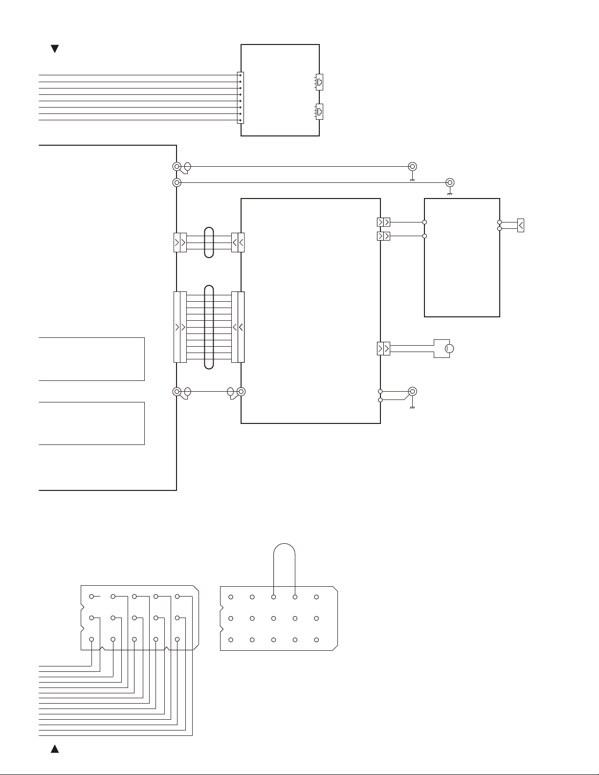
INTERCONNECTION DIAGRAM
FINAL UNIT
(X45-392) (C/3)
1
N_SYNC1_B
N_SYNC1_A
N_SYNC2_B
N_SYNC2_A
N_SYNC1_B
N_SYNC1_A
N_SYNC2_B
N_SYNC2_A
8
N SYNC2
J401
J402
N SYNC1
NXR-710
TX-RX UNIT
(X57-794)
SUB UNIT (RX VCO/PLL)
(X58-507)
SUB UNIT (TX VCO/PLL)
(X58-508)
CN101
CN500
CN701
GND
CN801
GND
8TC
RAMP
ASWC
FAN
FDT
TMP2
TMP1
PLIM
H/L
HWV2
CN610
RX ANT
Ext IN
CN201
W3
1
+B
+B
3
W4
11
1
W5
11
1
3
1
CN203
GND
+B
+B
CN204
GND
8TC
RAMP
ASWC
FAN
FDT
TMP2
TMP1
PLIM
H/L
HWV2
CN1
FINAL UNIT
(X45-392) (A/3)
+B
GND
CN202
CN205
FAB
FAG
W1
W2
+B
GND
+B1
GND
+
MAIN DC
–
FINAL UNIT
(X45-392) (B/3)
1
2
TX ANT
M
FAN
ER_CLK
MON
PTT
C
ER_DAT
XG
1
2
3
4
5
6
TEST/SPKR (PANEL VIEW)
6
3
2
1
915
5
74
12
14
118
10
13
129
77
Page 78
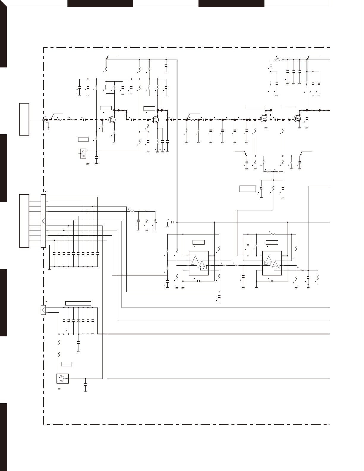
A B C D E
NXR-710
1
FINAL UNIT (X45-3920-10) (A/3)
2
T:0dBm
CN1
R2
CN204
11
10
9
8
7
6
5
4
3
2
1
C230 1000p
C231 1000p
0
C232 1000p
TX-RX UNIT
(X57-7940-10)-CN610
3
HWV2
H/L
PLIM
TMP1
TMP2
FDT
FAN
TX-RX UNIT
ASWC
RAMP
4
(X57-7940-10)-CN801
8TC
GND
C233 1000p
100n
L19
C234 1000p
SCHEMATIC DIAGRAM
T:7.96V
R:0V
C21
10
R17
L4
R19
C17
68n
2.7k
Q2
R18
470
C16
1000p
R20 22
C99 5p
C18 1000p
-t
10k
3.3k
TH201
R201
R202
C252
C4
1000p
RF SW
D1
1SS226-F
C235 1000p
C236 1000p
1000p
C14
R225
22
R14
R15
4.7k
1000p
RF AMP
2SC3357-A
C12
18p
1k
R16
0
C216
R226
1000p
R8
33
R6
1000p
C244 1000p
R7
C7
C247 1000p
L3
4.7k
RF AMP
Q1
2SC3357-A
0
R9
1k
1000p
C10
R10
270
56n
27
R11
C6
0.1u
C5
C237 1000p
1000p
1000p
C19
12p
C250
1000p
33k
100k
1000p
R203
R204
T:13.2V
F1
3.0A
L8
C37 1u
L9 47n
C33 1000p
100k
R28
0
DC AMP
IC202
C207
1000p
R208
R215
56k
C34
470p
R29
0
100
VCC
FINAL AMP
Q4
PD70HVF1-101
R30
100
R31
R32
100k
C205
1000p
8
7
6
5
TX DRIVE AMP
56p
VOLTAGE
REFERENCE
C253
PD55003S-E
22p
C98
C28
1000p
0.1u
1000p C206
R25
R26
Q3
R213
47
150k
R27
D201
560k
1
2
3
4
02DZ6.2F-Y
TA75W01FUF
VEE
T:23dBm
R23
18
270
R24
R21
DC AMP
IC201
TA75W01FUF
47k
1
2
3
4
VEE
27k
C201
1000p
C24
1000p
270
VCC
L5
L6
27n
12nL718n
27p
47p
C25
C26
C27
T:3.33V
R:0V
R205
100k
8
7
6
5
R206
R207
150k
100k
R210
100k
R:13.6V
C43 22p
C44 100p
C53 1u
C51 1000p
L10 47n
C52
240p
T:2.76V
R:0V
C45
100k
1000p
R217 150k
R219
100k
12k
R237
C210
1000p
R218
100k
5
6
7
FAB
FAG
78
X45-392 1/2
CN205
1
2
SURGE PROTECTOR
C238 1000p
10
R235
10
R236
DC SW
Q207
DTD123EK
C239 100u50
C251
D203
D203 1SS355
C240 22p
C241
C243 1000p
1000p
C242
C246 0.1u
C245 22p
1000p
1000p
Page 79

FINAL UNIT (X45-3920-10) (A/3)
C61 22p
C65 100p
SCHEMATIC DIAGRAM
CN2 CN3 CN4 CN5
NXR-710
JIHGF
1
C54 130p
R220
220k
82
82
R38
D10
MA2S111-F
RF DETECTOR
R41
L13
R40
0
R39
270n
0
RF DETECTOR
HSM88AS-E
C69
100
C71
D4
1000p
1000p
ANT SW
C78
470p
5T
C82
1000p
18p
L15
D7
L7091CER
D7,8
RF SW
D8
L7091CER
C80
27p
L14
9.5T
C75
R42
120
C63
33p
L11
22n
C57 82p
R221
18k
C249
1000p
C68
470p
RF DETECTOR
HSM88AS-E
R36
L12
270n
0
R34
D3
0
R35
C66
1000p
0
R12
C60
1000p
R33
82k
T:47dBm
L17
L16
47n
C84 15p
R44
C97
0
1000p
L18
47n
47n
D9
C88 27p
C89 18p
C91 27p
C92 22p
CSA70-401L
C94 22p
D9
SURGE PROTECTION
C229
1000p
R43
220k
CN203
TX ANT
RX
1
GND
2
+B
3
+B
TX-RX UNIT
(X57-7940-10)-CN701
FINAL UNIT (X45-3920-10) (B/3)
VOLTAGE
REGULATOR
NJM78M08FA-ZB
1
IN3oUT
C218 0.1u
IC203
GND
2
C219 1000p
C220 10u35
D202
SURGE PROTECTOR
C224
D202
R228
C223
47k
R230
4.7k
8V
DC SW
Q203
2SJ484
1000u35
22ZR-10D
DC SW
Q205
SSM3K15TE(F)
1000p
C225
CN201
0.1u
CN202
GND
W1
+B
+B
TERMINAL
W2
GND
C301
PROTECT of REVERSE
CONNECTION
470p
D301
D301
DSA3A1
CN301
+B
470p
DC CONNECTOR
GND
C302
B
2
3
4
5
C248
1000p
470k
C222
R232
1000p
DC SW
Q204
2SJ484
R351
47k
R229
R231
4.7k
C23
1000p
0
R354
0
DC SW
Q206
SSM3K15TE(F)
R233
C221
1000p
470k
Note : The components marked with a dot (•) are parts of layer 1.
FINAL UNIT (X45-3920-10) (C/3)
J401
123
J402
4
123
4
N_SYNC1_B
1
N_SYNC1_A
2
N_SYNC2_B
3
N_SYNC2_A
4
N_SYNC1_B
5
N_SYNC1_A
6
N_SYNC2_B
7
N_SYNC2_A
8
CONTROL UNIT
(X53-4490-10)-CN5
6
7
79
X45-392 2/2
Page 80

A B C D E
NXR-710
CONTROL UNIT (X53-4490-10)
1
CN301
SB
3
2
2
3
4
5
6
+B
GND
TX-RX UNIT
(X57-7940-10)-CN700
N_SYNC1_B
N_SYNC1_A
N_SYNC2_B
N_SYNC2_A
N_SYNC1_B
N_SYNC1_A
FINAL UNIT
N_SYNC2_B
(X45-3920-10)(C/3)
N_SYNC2_A
1
CN5
1
2
3
4
5
6
7
8
C8
SCHEMATIC DIAGRAM
SB
VOLTAGE
REGULATOR
IC302
R310
R309
R313
8.2k(D)
R315
C312
D302
L312
0.022u
22
22
470
C22
0.1u
XC6201P502PR
3
VIN1VOUT
C314
1000p
47u25
VOLTAGE
REGULATOR
IC303
XC6204B332P1
C318 1000p
C317 47u25
C319
C315
47u25
C320
C316
47u25
R314
C333
3.3k(D)
VOLTAGE REFERENCE
D303
02DZ18F-X
BUFFER
IC7
TC7WT125FUF
0.1u
BUFFER
IC8
TC7WT125FUF
VSS
2
1000p
1000p
0.1u
8
VCC
G1
1
8
VCC
G1
1
R306 180k(D)
R307
L306
SURGE PROTECTOR
60DC
C311 33u16
C310 33u16
R308 47k
D302 1SS388F
C313
27k(D)
45
3
R22
100k
2
1
10k
R25
C21
45
3
R23
100k
2
1
R26
10k
13.6V13.6V
L301
L302
L303
R301
L313
L314
C301
100p
0
R302
0
6.0V
BooST
R305
0.1u
50M
C19
0.1u
C308
0.47u
1BD2
18k
D301
SURGE PROTECTOR
RS-485
TRANSCEIVER
ISL8485EIBZ
GND
6
A/Y
7
B/Z
8
VCC
RS-485
TRANSCEIVER
ISL8485EIBZ
GND
6
A/Y
7
B/Z
8
VCC
D301
IC4
IC5
L305
RSX301L-30
DI
DE
RE
Ro
DI
DE
RE
Ro
L304
C302
47u35
47u35
C303 4.7u
C304 4.7u
R12
100
R13
100
C7
C9
C13
100p
100p
R10 100
R11 100
C10
C12
100p
DC/DC
CONVERTER
IC301
LT3685EMSE
C15
100p
C14
100p
R303
5
SYNC7PG8FB9VC10RT11GND
6
L2
L33-1500-05
100p
L3
L33-1500-05
100p
100k
RUN/SS
3SW4
VIN
22k
R304
C306
470p
C18
C335
G2
2A13Y24
G2
2A13Y24
4
VIN
470p
C321
1000p
VSS3CE
1
2
3
1
2
3
5A26Y17
GND
5A26Y17
GND
L307
C322
47u25
5
VoUT
C323 1000p
1NC2
VOLTAGE
REGULATOR
IC304
XC6205B152PRN
NC
VSS
CE4VIN
VOLTAGE
REGULATOR
IC305
XC6205B162PR
NC
VSS
CE4VIN
VOLTAGE
REGULATOR
IC307
XC61CN2702N
2
IN
NC
3
Q301
RT1N441U-T111
DC SW
L308
C324 47u25
VoUT
VoUT
1
4
TC7SH125FU-F
1
G
2
3
1
2
3
5
5
oUT
VSS
BUFFER
IC10
INA
GND4oUTY
C35
0.1u
BUFFER
IC11
TC7SH125FU-F
G
INA
GND4oUTY
C36
0.1u
5.0V
50M
1000p
POWER SW
2SA1955A-F
15M
16M
RXD1
TXD1
TXD3
RXD3
3.3V
L316
C332
47u25
AA
3.3V
D304,305
SURGE
PROTECTOR
Q303
10k
R319
/RST
/BiNT
/oVRB
33M
D305
1SS388F
R321
2.7k(D)
1k
R323
D304
1SS388F
R322
CN302
47k(D)
33M
33M
50M50M
VOLTAGE
REGULATOR
IC306
XC6204B332P1
1
5
NC
VoUT
2
VSS
3
CE4VIN
A
L315
C327
47u25
3.3V
VOLTAGE
REGULATOR
IC308
XC6109C29ANN
R316
1
L311
VCC
VCC
VIN
1000p
1000p
4.7k
1000p
VoUT
C334
0.01u
2
VSS
C336 0.01u
L309
C328
47u25
R324
C329
47u25
4.7k
R318
C470
1000p
R42
100k
R41
100k
0
C325
C326
R317
C337
5
5
C331
C330
1000p
AA
DC SW
Q302
SSM3K15TE(F)
4
3
CD
R320
100
C471
1000p
1.5V
1.6V
0
R44
/485_RE1
0
R45
0
R46
0
485_DE1
R47
0
R48
0
R49
0
/485_RE2
R50
0
R43
485_DE2
0
J19-5386-05
SB
15M
33BU
33M
50M
33A
16M
7
80
X53-449 1/6
Page 81

CONTROL UNIT (X53-4490-10)
SCHEMATIC DIAGRAM
NXR-710
JIHGF
SBSB
15M
33BU
33M 33M
33A 33A
0.1u
0.1u
0.1u
1u
0.1u
0.1u
CVDD_1
DVDD_10
HA[1]/HCNTL1
RST_MoDE
RESET
T12
G16
100k
R34
1000p
DVDD_9
DVDD_1
NMI
R11
100k
R35
R37
10k
R36
100k
C38
C39
M17A7A3F1U12U4R1
DVDD_8
CLKIN
HA[0]
INT5
P12
100k
R38
C41
DVDD_7
INT4
T14
100k
R40
C42
DVDD_6
INT3
R13
0.1u
C43
DVDD_5
INT2
U13
DVDD_4
INT1
C44
C46
C45
U14
U6N1D17D1A12
DVDD_2
DVDD_3
HA[4]
HA[3]
HA[2]/HAS
CLKX2
FSX2
CLKS2R7DR2R6FSR2R5CLKR2
INT0
P8
R12
100k
R51
R52 22
D16
F16
HA[6]
HA[7]
HA[8]
HA[9]
HA[10]
HA[5]
HA[11]
HA[12]
HA[13]
HA[14]
HA[15]
HA[16]
HA[17]
HA[18]
HA[19]
HD[0]
HD[1]
HD[2]
HD[3]
HD[4]
HD[5]
HD[6]
HD[7]
HD[8]
HD[9]
HD[10]
HD[11]
HD[12]
HD[13]
HD[14]
HD[15]
HDS2
HDS1
HBE1
HBE0
HCNTL0
HRDY
HINT
HR/W
HMoDE
CLKX0
FSX0
CLKR0
FSR0
CLKS0
CLKX1
FSX1
CLKR1
FSR1
CLKS1
100k
R53
R57 100k
R55 100k
R56 100k
R54 100k
C47 1000p
A[0]
E16
F15
G15
H14
J14
K17
J16
G14
F14
E15
D15
E14
G17
H16
J15
K16
M15
M14
N17
B16
B13
B11
B15
C9
C10
C11
C12
C13
C14
A15
D13
D12
D11
D10
D9
D14
B17
C16
HCS
M16
R59 0
K15
R60 0
N15
R61 0
B14
R62 100
N14
C15
R63 0
N16
U7
R64 100
P9
R10
R65 100
DX0
U3
T5
R66 0
R67 0
T6
DR0
U5
R68 0
R15
R69 0
T15
T16
R58 100
DX1
T3
R2
R70 0
P3
DR1
P2
U8
R71 0
R72 0
R9
DX2
R73 0
U11
CN15
CN16
CN17
C50 0.1u
CN18
CN19
R75 100k
CN20
CN21
AND GATE
TC7SH08FU-F
1
INB
2
INA
3
GND4oUTY
A[1]
A[2]
A[3]
A[4]
A[5]
A[6]
A[7]
A[8]
A[9]
A[10]
A[11]
A[12]
A[13]
A[14]
A[15]
A[16]
A[17]
A[18]
A[19]
D[0]
D[1]
D[2]
D[3]
D[4]
D[5]
D[6]
D[7]
D[8]
D[9]
D[10]
D[11]
D[12]
D[13]
D[14]
D[15]
A[20]
IC12
5
VCC
/HDS2
/RD
/CS3
/HRDY
/WR
/MCCSXCN
MCDiCN
/MCCSRCN
MCDoCN
MCSCKAF
/MCCSAF
MCDiAF
MCDoAF
BiCK
LRCLK
SDTi
L6
R77
MCSCKCN
150
L3
K3
K2
E4
CE3
G1
CE2
H2
CE1
J2
CE0
B8
A[0]
D8
A[1]
B7
A[2]
C7
A[3]
A6
A[4]
C6
A[5]
C4
A[6]
C5
A[7]
A4
A[8]
A2
A[9]
C1
A[10]
E1
A[11]
F3
A[12]
F2
A[13]
G4
A[14]
G3
A[15]
F4
A[16]
G2
A[17]
H4
A[18]
H3
A[19]
J4
A[20]
J3
A[21]
C8
D[0]
D7
D[1]
A8
D[2]
B6
D[3]
D6
D[4]
B5
D[5]
D5
D[6]
B4
D[7]
D4
D[8]
B3
D[9]
C3
D[10]
D3
D[11]
E3
D[12]
C2
D[13]
D2
D[14]
E2
D[15]
N3
D[16]
T1
D[17]
R3
D[18]
P4
D[19]
R4
D[20]
T4
D[21]
P5
D[22]
P6
D[23]
P7
D[24]
T7
D[25]
R8
D[26]
T8
D[27]
P11
D[28]
T9
D[29]
T10
D[30]
P10
D[31]
K1
L4
R15
100k
U15
R14
P14
U16B9L4
BE3
AoE
BE2
ARE
HoLD
HoLDA
CLKMEM
BE1
BE0
IO[7]L2IO[6]M1IO[5]N2IO[4]P1IO[3]/BooTM2T2IO[2]/BooTM1M4IO[1]/BooTM0
R14 0
T13
AWE
IO[0]E5BooTM3B2XF
K4
R18
ARDY
CN6
100k
A11M2M3N4P13
SSoE
SSWE
SSADS
SDRAS
NC_1N9NC_2N5NC_3L5NC_4J5NC_5G5NC_6
T11
CN8
CN9
CN10
CN11
CN12
CN13
CN7
U17U9U1
T17
U10U2J1
A16
H17H1B1
A10
J17
A17A9A1
B10
B12
A13
SDCAS
SDWE
SDA10
E12
VSS_17
NC_7E8NC_8
VSS_16
N12
VSS_14
VSS_15
NC_9N8NC_10
VSS_11
VSS_12
VSS_13
NC_11
NC_12N7NC_13M5NC_14H5NC_15E9NC_16
E11
N11
VSS_10
VSS_9
VSS_8
E13
VSS_7
RSVD[9]
F13
VSS_6
RSVD[8]
G13
VSS_4
DSP
RSVD[7]
H13
VSS_3
IC6
RSVD[6]
J13
VSS_2
RSVD[5]
K13
16M
33M_1
CP1
RK74HB1J334J
CP2
RK74HB1J334J
CP3
RK74HB1J334J
CP4
RK74HB1J334J
CP5
RK74HB1J334J
CP6
RK74HB1J334J
CP7
RK74HB1J334J
CP8
RK74HB1J334J
33M_1
ED[18]
ED[21]
ED[22]
ED[23]
ED[24]
ED[25]
ED[26]
ED[27]
ED[29]
ED[31]
ED[30]
ED[28]
ED[10]
ED[13]
ED[14]
ED[11]
ED[15]
ED[12]
ED[16]
ED[19]
ED[20]
ED[17]
ED[0]
ED[1]
ED[2]
ED[3]
ED[4]
ED[5]
ED[6]
ED[2]
ED[7]
ED[0]
ED[8]
ED[1]
ED[4]
ED[9]
ED[10]
ED[11]
ED[12]
ED[3]
ED[5]
ED[13]
ED[6]
ED[14]
ED[7]
ED[15]
ED[16]
ED[17]
ED[8]
ED[18]
ED[9]
ED[19]
ED[20]
ED[21]
ED[22]
ED[23]
ED[24]
ED[25]
ED[26]
ED[27]
ED[28]
ED[29]
ED[30]
ED[31]
R3 100k
R4 100k
R5 100k
R6 100k
R7 100k
R8 100k
R9 100k
VSS_1
RSVD[4]
L13
CVDD_14
CVDD_15
RSVD[3]
RSVD[2]
M13
N10N6A5
CVDD_13
RSVD[1]
N13
C260 0.1u
R17
47k
R27
C23 0.1u
CVDD_11
CVDD_12
TIN/ToUT1
TIN/ToUT0
P15
47k
R28
C24 0.1u
P16
0
R29
C25 0.1u
CVDD_9
CVDD_10
CLKMD
CLKoUT
H15
CN14
C26 0.1u
K14
C27 0.1u
CVDD_8
TMS
L17
C28 0.1u
CVDD_7
TCK
C17
C29 0.1u
CVDD_6
TRST
L16
C30 0.1u
P17L1F17E7K5F5E10E6A14
CVDD_5
TDI
L15
C32 0.1u
CVDD_4
TDo
L14
R32 4.7k
C34 1u
C33 0.1u
CVDD_2
CVDD_3
EMU1/OFF
EMU0
E17
R16
4.7k
R33
33M_1
/HINT
15M
33BU
50M50M
A[21]
CN4
L1
FLASH MEMORY
E29PL03270TIP
A[16]
47NC48
A16
IC3
A152A143A134A125A116A107A98A89A1910A2011WE
1
A[14]
A[15]
D[7]
D[2]
oE
NC2
NC3
DQ2
DQ7
SRAM
IC9
CE2A4A3A5A6A6A8B1DQ4B2A2B3WE
/DRST
D[6]
DQ6
/PCS_DSP
/PDN
BER_DATA
BER_CLK
/BER_EN
FSDET
D[1]
D[15]
1u
C11
45
46
VSS2
DQ15
A[12]
A[13]
D[12]
38
39
40
41
42
43
44
DQ7
A[11]
A[10]
DQ4
DQ5
DQ6
DQ12
DQ13
DQ14
/WR
A[20]
A[19]
A[8]
A[9]
D[4]
D[5]
D[6]
D[7]
D[13]
D[14]
D[9]
D[2]
D[3]
D[11]
D[10]
34
35
36
37
DQ3
VCC
DQ10
DQ11
RESET13A2114WP/ACC15RY/BY16A1817A1718A719A620A521A422A323A224A1
12
/FRST
/WP
A[17]
A[18]
A[7]
A[0]
D[0]
D[8]
/RD
/CS0
0
R24
1u
C20
27
28oE29
25A026
CE
DQ030DQ831DQ132DQ933DQ2
VSS1
A[4]
A[5]
A[6]
A[2]
A[3]
A[1]
D[3]
/RD
/CS2
G2
G3
CE
A[16]
G4
A16
A[15]
G5
A15
G6
DQ3
A[9]
H1
A9
A[10]
H2
A10
A[11]
H3
A11
A[12]
H4
A12
A[13]
H5
A13
A[14]
H6
A14
A1A0A2A1A3
A[0]
A[1]
A[3]
A[6]
A[8]
A[2]
/SYMTiM
/DINT
/DWUP
A[5]
A[4]
A[7]
D[4]
D[5]
D[1]
D[0]
3.3V
1000p
/WR
L5
/RST
C40
1u
E1E6F1F3F4F6G1
D6
VSS2
VCC2
VCC1
D1
VSS1
C6
DQ1
C4
A5
C3
NC1
C1
DQ5
B6
DQ0
B5
A7
B4
A4
C31
R30
470k
81
X53-449 2/6
Page 82

K L M N O
NXR-710
SB
15M
33BU
33M
50M
33A
33M_1
L18C77
3.3V
R114
22
C76
47p
0.1u
22
R115
C18
F15
R13
T16
T17
F3
J4
D5
A4
IFIR
MICIR
B4
STR_SEL
A[0]
A[1]
A[2]
A[3]
A[4]
A[5]
A[6]
A[7]
A[8]
A[9]
A[10]
A[11]
A[12]
A[13]
A[14]
A[15]
A[16]
A[17]
A[18]
A[19]
A[20]
A[21]
D[0]
D[1]
D[2]
D[3]
D[4]
D[5]
D[6]
D[7]
D[8]
D[9]
D[10]
D[11]
D[12]
D[13]
D[14]
D[15]
/WR
/RD
/DWUP
/485_RE1
/CS3
/CS2
/485_RE2
/CS0
/HRDY
/HDS2
TXD0
RXD0
TXVCoA
TXD1
RXD1
TXD2
RXD2
TXD3
RXD3
A10
A12
B11
A11
H18
J18
K18
L18
M18
N18
J17
K17
M17
N17
P17
K16
L16
M16
P16
J15
K15
M15
N15
P15
J16
H15
G17
H16
G15
F18
F17
G16
E18
E17
F16
D18
D17
B15
D16
C15
D15
E15
A15
A16
B14
C14
A13
D13
C13
B13
A14
B12
D14
R18
T18
R16
R15
U15
T15
V15
V14
T14
R116 4.7k
R117 4.7k
33M_2
32K
/RST
32I
DSPCK
CKo
USRCKI
ADD0
ADD1
ADD2
ADD3
ADD4
ADD5
ADD6
ADD7
ADD8
ADD9
ADD10
ADD11
ADD12
ADD13
ADD14
ADD15
ADD16
ADD17
ADD18
ADD19
ADD20
ADD21
DT0
DT1
DT2
DT3
DT4
DT5
DT6
DT7
DT8
DT9
DT10
DT11
DT12
DT13
DT14
DT15
WRITE
READ
BHE
BLE
CS4
CS3
CS2
CS1
CS0
HRADY
HDS2
TXD0
RXD0
RTS0
CTS0
TXD1
RXD1
TXD2
RXD2
TXD3
R14
i2CCK
32K
/RiNT
/HINT
NC25
NC26
NC27
NC28N4NC29T1NC30
ADC1
XTALI
XTALo
RXD3A9SCK
SDTV4SPCK0U5SPI0T6SPo0V5SPCS00U4SPCS01T4SPCS02V6SPCK1U7SPI1T8SPo1V7SPCS10U6SPCS11T5SPCS12G3ADC4H1ADC5H2ADC6H3ADC7J1ADC8J2ADC9J3MICVR
C10
/TXPCS
SPSD0
/RXPCS
SPSCLK1
SPSCLK0
/16_8PCS
i2CDA
SCHEMATIC DIAGRAM
IC16
NC24
C16
NC23
TXVCoB
SM5023CNDH-G
4
Q
5
VDD
6
XTN
BUFFER AMP
B16
SPSD1
/ioCS
/EVCS
R119
470k
NC20D4NC21D6NC22
/EVDSCS
INHN
R129 100
RX_CV
3
VSS
2
XT
1
R130 100
HWV1
TX_CV
186mVrms
TMP2
HWV3
0.01u
VLi
C79
V18
L77-3015-05
U18
V17
NC10
NC11
NC12U1NC13U2NC14V1NC15V2NC16A3NC17C3NC18C5NC19
SPDACK2MICADC0K3MoDDAC
K1
TXAF
X1
C91
0.1u
B18
U17
NC9
71mVrms
W:293mVrms
N:146mVrms
L2
MOD
B17
NC8
MICADC1
T10
/KEYi0
A18
NC6
NC7
KEYI0R9KEYI1
/KEYi1
R132
1k
C92
A17
NC5
MCU
IC20
KEYI2
KEYI3
KEYI4
KEYo0
V11
U10
T11
V12
CN24
CN25
KEYo0
/KEYi2
C97
R135
100k
0.01u
A1
NC1A2NC2B1NC3B2NC4
KEYo1
U11
T12
KEYo1
1000p
C98 0.1u
C99 0.1u
C101 0.01u
T3
K4
M1
U3
E5
NC35
NC34
AVCC8L3AVCC9
AGND2F5AGND3G5AGND4H5AGND5J5AGND6K5AGND7L1AGND8E6AGND9
AVCC10
KEYo2
KEYo3
KEYo4R4PWM1P4PWM2V8TI
TDI
TMS
TDo
TCK
TRST
RTCK
V13
U12
CN26
BSCAN0
R10
R12
R11
T13
U14
U13
H17
E16
CN28
CN27
R138 100k
R141 100k
BSCAN1
P18
R511 0
/RST
C103 1000p
R143 0
C102 1u
D3
V16
F4
NC36
AVCC4G4AVCC5H4AVCC6
TEST1
RST
RSTo
TEST0
N16
R17
G18
L17
/FRST
P13
P12
B3
A5
C17
U16
AVCC1E4AVCC2
DGND11C4DGND12T2DGND13
DGND14
DGND15
DGND4
DGND5
DGND6
DGND10
DGND7P8DGND8P7DGND9
MCCK1
MCCS0
MCo0
MCI0
MCCK0
AGCDAC
TEST2
TEST3V3BooTC2SQDACF1ADC0F2DAC0E1IFRG2ADC3G1ADC2D2FCDADCE2IFADCPE3IFADCND1IFVR
L15
R146 100
R147 100
R144 0
FWD
RSSi
RXASSiST
RAMP_TX
TXASSiST
TMP1
K14
DGND3
DGND2
DGND1
DVDIo7
DVDIo6
DVDIo5
DVDIo4
DVDIo3
DVDIo2
DVDIo1
DVDD10
DVDD9
DVDD8
DVDD7
DVDD6
DVDD5
DVDD4
DVDD3
DVDD2
DVDD1
GPIo11
GPIo10
GPIo9
GPIo8
GPIo7
GPIo6
GPIo5
GPIo4
GPIo3
GPIo2
GPIo1
GPIo0
SIMRST
SIMCK
SIMDT
SYMTIM
FSDET
TXRVE
TRAMP
PSTPA
PSTIF
PSTPLL
RXRVE
RXSLT
PSRRF
PSRIF
PSRPLL
RSSIT
VFRM
MCCS2
MCCK2
MCCR1
MCCX1
J14
TMoD
VoINT
MCo2
MCo1
MCI1
C110 100p
C111 100p
C112 0.1u
C109 10u63.3
R152 1k
CONTROL UNIT (X53-4490-10)
SB
15M
L20
3.3V
33M_2
E12
E11
E10
C115 0.1u
L5
C116 0.1u
P6
C117 0.1u
P11
C118 0.1u
L14
C119 0.1u
H14
C120 1u
E13
E7
M5
N5
P9
P10
N14
M14
G14
F14
E9
E8
B5
C6
B6
A6
U8
R8
R7
T7
CLKSEL
V10
U9
V9
T9
C11
D12
C12
R5
R6
R2
P3
P2
M4
R1
N3
N2
P1
L4
M2
M3
N1
D8
D7
C7
D10
C8
D9
B7
C9
B8
A7
B10
B9
D11
A8
R3
CN31
/MCCSRCN
/MCCSXCN
MCDoCN
MCDiCN
MCSCKCN
/MCCSAF
MCDoAF
MCDiAF
MCSCKAF
C114
100p
C121
C122 0.1u
C123 0.1u
C124 0.1u
C125 0.1u
C126 0.1u
C127 0.01u
C128 1u
C129 1000p
SBC
R154 100k
R155 100k
/SYMTiM
485_DE2
Ao4
Ao3
Ao2
485_DE1
Ao1
/DINT
/DRST
/HK
/ioiNT
LDT
LDR
/EPTT
1000p
/PTT
SR_STR
RXVCoA/B
/WP
Ao5
R159
AMP_SW
/AF_MUTE
R156
470k
R157
470k
C130
0.1u
C131
0.1u
FSDET
/EWP
/oVRB
10k
/PSW
/BiNT
TD_SW
100
R160
10k
R161
AGC
33M_1
AMP_SW
/AF_MUTE
33M_2
33BU
33M
50M
33A
SBC
32K
/RST
/RST
82
X53-449 3/6
oX_SDA
C82 100p
C83 100p
C85 6800p
C86 6800p
R126 100k
R127 1k
R128
C93
10u6.3
C94
0.1u
A
100k
C108
2p
R148
CN29
R153 47k
56kC84 6800p
CN30
MOD
TXAF
Page 83

SCHEMATIC DIAGRAM
NXR-710
CONTROL UNIT (X53-4490-10)
LDR
33BU
33M
33A 33A
33M_1
0
R79
33BU
32K
33M
/FRST
AMP_SW
/AF_MUTE /AF_MUTE
33M_2 33M_2
32K
/RST
i2CCK
i2CDA
C56
C57
/RiNT
TXD2
TXD0
TXD2_DiS
SPSCLK1
SPSD1
/PTT
i2CCK
i2CDA
/ioiNT
RXD0
/EPTT
RXD2
/HK
CN22
CN23
242mVrms
R81
100k
C60
C62
0.1u
1000p
C63
C61
0.1u
1000p
R82
100k
SURGE
PROTECTOR
R510 10k
R122 10k
R118
0
CODEC
IC14
AK4386VTP
8
DEM9DIF0
7
10
DFS1
RoUT
6
11
DFS0
LoUT
5
12
10u
10u
R509
D3
R121
R124 10k
R508 10k
22k
1SS388F
100k
13
14
15
16
1
2
3
4
5
1
2
3
4
5
6
7
8
9
10
1
2
3
4
5
6
7
8
9
10
VCoM
LRCK
VSS
SDTI
VDD
BICK
DIF1
MCLK
TEST
C81 1000p
C80 0.01u
RTC IC
IC17
R2023T
32KoUT
SCL
oSCIN
oSCoUT
SDA
INTRB
CLKC
INTRA
VSS
R123
47k
C89 1000p
C90 0.1u
BUFFER
IC18
TC74VHCT244AFK
1G
1A1
2Y4
1A2
2Y3
1A3
2Y2
1A4
2Y1
GND112A1
3.3V 5V
(A)
C87 1000p
C88 0.1u
BUFFER
IC19
TC7MBD3245AFK
NC
VCC
A1
A2
A3
A4
A5
A6
A7
A8
GND
3.3V 5V
PDN
4
3
2
1
L7
10
VDD
9
8
7
6
20
VCC
19
2G
18
1Y1
17
2A4
16
1Y2
15
2A3
14
1Y3
13
2A2
12
1Y4
(Y)
20
19
oE
18
B1
17
B2
16
B3
15
B4
14
B5
13
B6
12
B7
11
B8
/PDN
SQDAC
10
D2
MA2S111-F
10k
R101
R104
39k
C72
R103
0.22u
A
NAND GATE
TC7WT125FUF
1
G1
2
A1
3
Y2
4
GND
C107 0.1u
C105 0.1u
C106 0.1u
RS-232C
DRIVER/RECEIVER
ADM101EARMZ
1
GND
2
C1-
3
V-
4
TIN
5
RoUT6RIN
C104
0.1u
R145
5
6
7
VSS
VDD
NC_1
I/O EXPANDER
IC22
MCP23017TE/ML
INTB16INTA17GPA018GPA119GPA220GPA321GPA4
15
Ai2
Ai1
R106
R110
6.8k
AF AMP
IC15
TC75W51FK(F)
10k
R107
180k
100k
330k
R108
R105
-t
TH1
100k
A
IC23
8
VCC
7
G2
6
Y1
5
A2
IC21
10
VCC
9
C1+
8
SD
7
ToUT
AUXio6
AUXio5
100k
1
28
GPB42GPB53GPB64GPB7
GPB3
27
GPB2
26
GPB1
25
GPB0
R149 100k
24
GPA7
R150 100k
23
GPA6
R151 100k
22
GPA5
SC
Ai3
EXT_MoN
R111
100k
C73
47p
45
VSS
IN+A
IN+B6IN-B7oUTB8VDD
R109
100k
BER_DATA_5V
R113
123
IN-A
oUTA
C74
100p
R112
100k
BER_CLK_5V
TXD0_RSo
RXD0_RSi
AUXio4
AUXio3
AUXio2
AUXio1
1k
A
C75
0.1u
EXT_RSSi
RSSi
1u
C64
R85
C52
R78
C51
1k
1u
27p
A
R80
82k
45
VSS
IN+B6IN-B7oUTB8VDD
R282
100k
10k
C58
680p
123
IN-A
IN+A
R83
100k
oUTA
1000p
C65
C66
0.01u
330k
Q4
2SC4617(S)
DC SW
C67
/EPTT_5V
10
R88
DETECTOR
C68
R89
3.3k
0.01u
A
C70
R87
0.22u
D1
RB706F-40
C69
1000p
DETECTOR
R90
470
0.1u
A
/BER_EN
BER_CLK
BER_DATA
0.1u
C100
R142
100k
8
SCL
9
SDA
10
NC_2
11
A0
12
A1
13
A2
14
RESET
R93 100k
R95 22
L77-1802-05
50M
4.7k
R99 100k
R100 100k
R102 100k
R94
100k
AF AMP
100k
R312
BiCK
SDTi
LRCLK
X2
C95
2p
C96
2p
SPSCLK1_DiS
SPSD1_DiS
R137
100k
R133
4.7k
RXD2_DiS
TC75W51FK(F)
C49
1u
SR_oE_DiS
IC13
R74
100k
A
/FRST_io
TXD0_RSi
i2CCA_5V
i2CDA_5V
RXD0_RSo
R92 100k
3.3V
R131
TSRQP
SBSB
33M
50M50M
SBCSBC
AMP_SW
MOD
TXAF
MOD
TXAF
83
X53-449 4/6
Page 84
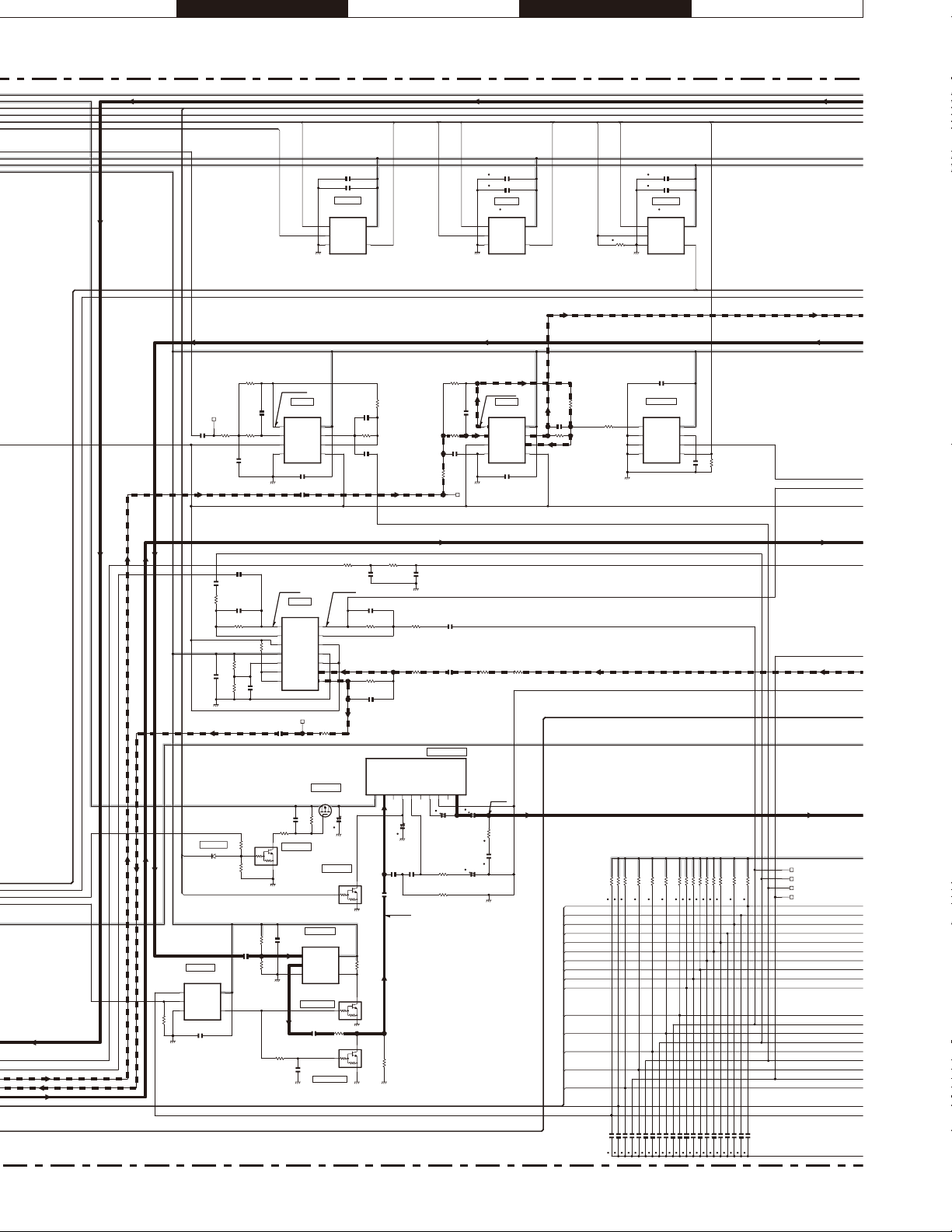
U V W X Y
NXR-710
SB
33M
33A
SBC
CN401
C409
100u
MOD
SCHEMATIC DIAGRAM
/RXPCS
/PCS_DSP
C132 0.01u
C133 1000p
AND GATE
IC24
TC7SH08FU-F
1
INB
2
INA
3
GND4oUTY
R425
22k
242mVrms
OP AMP
IC406
NJM2732V
330p
C424
1
8
AoUTPUT
R413
R422
22k
22k
C419
1500p
V+
2
7
A-INPUT
BoUTPUT
3
6
A+INPUT
B-INPUT
4
5
GND
B+INPUT
C429
0.1u
A
C408
100u
/RXPCS_TR
5
VCC
R441
100k
C436
220p
R437
33k
C438
100u
STR_SEL
R412
2200p
R414
R415
C417
12k
15k
12k
CN402
/EVDSCS
C418
390P
1
2
3
1
2
3
4
A
W:366mVrms
N:183mVrms
C134 0.01u
C135 1000p
OR GATE
IC25
TC7SH32FU-F
INB
INA
GND4oUTY
OP AMP
IC404
NJM2732V
AoUTPUT
A-INPUT
BoUTPUT
A+INPUT
B-INPUT
GND
B+INPUT
C426
0.1u
CONTROL UNIT (X53-4490-10)
SB
SR_STR
/EVDSCS_EV
5
VCC
R435
C433
8
180p
V+
7
R432
33k
6
5
STR_SEL
C136 1000p
C137 0.01u
AND GATE
IC26
TC7SET08FU-F
1
INB
2
INA
R162
3
GND4oUTY
100k
C443
0.1u
47k
ANALOG SW
IC407
TC7W53FK(F)
R439
1
CoMMoN
47k
2
INH
3
VEE
4
GND5A
A
TD_SW
33M
50M50M
5
VCC
SR_STR_DiS
8
VCC
7
CH0
6
CH1
1u
47k
C451
R450
RD
SBC
MOD
33A
VREF
SBC
AMP_SW
/AF_MUTE
33M_2
MOD
TXAF
TA TA
C469
1u
1u
C414
R416
220k
C420
220p
R421
R417
10u
C412
R418
A
TXAF
33M_2 33M_2
AMP_SW
DIODE SW
D401
/oVRB
1SS388F
/PSW
NAND GATE
IC401
TC7SH00FU-F
1
5
INB
VCC
2
INA
3
GND4oUTY
47k
R401
C401
0.01u
A
39k
100k
100k
C421
R402
4.7k
47k
R403
C403
1u
50mVrms 177mVrms
OP AMP
NJM2734V
1
AoUTPUT
2
A-INPUT
3
A+INPUT
0
4
R420
V+
5
B+INPUT
6
B-INPUT
7
BoUTPUT
10u
C428
1u
C402
R404
4.7k
POWER SW
Q401
RT1N141M-T111
A
R406
100k
C405
0.1u
R407
100k
A
R408
10k
IC405
CN403
C406
14
DoUTPUT
13
D-INPUT
12
D+INPUT
11
GND
10
C+INPUT
9
C-INPUT
8
CoUTPUT
R431
0
POWER SW
Q402
2SJ506-E(S)
47k
R405
100p
C404
POWER SW
Q403
RT1N441M-T111
ANALOG SW
IC402
TC7S66FUF
1
IN/oUT
VCC
2
oUT/IN
3
GND4CoNT
AF MUTE SW
Q404
RT1N141M-T111
C407
R409
1u
10k
Q405
1u
DTC363EU
AF MUTE SW
A A
R424
R426
15k
10k
C427
C413
1000p
C410
R411
A
1u
50mVrms
4.7k
4DC5
C415
IC403
LA4422-E
47u25
A
C416
1000p
470p
A
C441
R438
100u
100k
R442
C442
68k
1u
AF POWER AMP
NFA6NFB7BS8GND9NC210OUT
C425
47u25
R423
470
R419
1M
SPM
C430
1000u25
C422
47u25
TD
R443
R457
0
0
4Vrms
at 4W
2.7
R430
0.1u
C432
A
BER_CLK_5V
RXD0_RSi
EXT_MoN
TXD0_RSo
/EPTT_5V
Ai1
SC
Ai2
BER_DATA_5V
Ai3
AUXio1
AUXio2
AUXio3
AUXio4
AUXio5
AUXio6
R167 47k
R174 47k
R173 47k
R169 47k
R168 47k
R171 47k
R182 47k
R181 47k
R185 47k
R180 47k
R183 47k
R178 47k
R176 47k
R177 47k
R187 47k
C423
470p
C434
100p
R433
100k
R436
120k
C435
100p
VCC2IN3NC1
1
470u35
A
A
5
R410
100k
A
RA
SPoSPo
50M
CN32
CN33
CN34
CN35
84
X53-449 5/6
C144 1000p
C145 1000p
C142 1000p
C139 0.01u
C141 1000p
C150 0.01u
C147 0.01u
C143 0.01u
C146 1000p
C151 1000p
C149 1000p
C152 1000p
C153 1000p
C154 1000p
C155 1000p
C157 1000p
C161 1000p
C164 1000p
C160 100p
C159 0.01u
C162 100p
Page 85
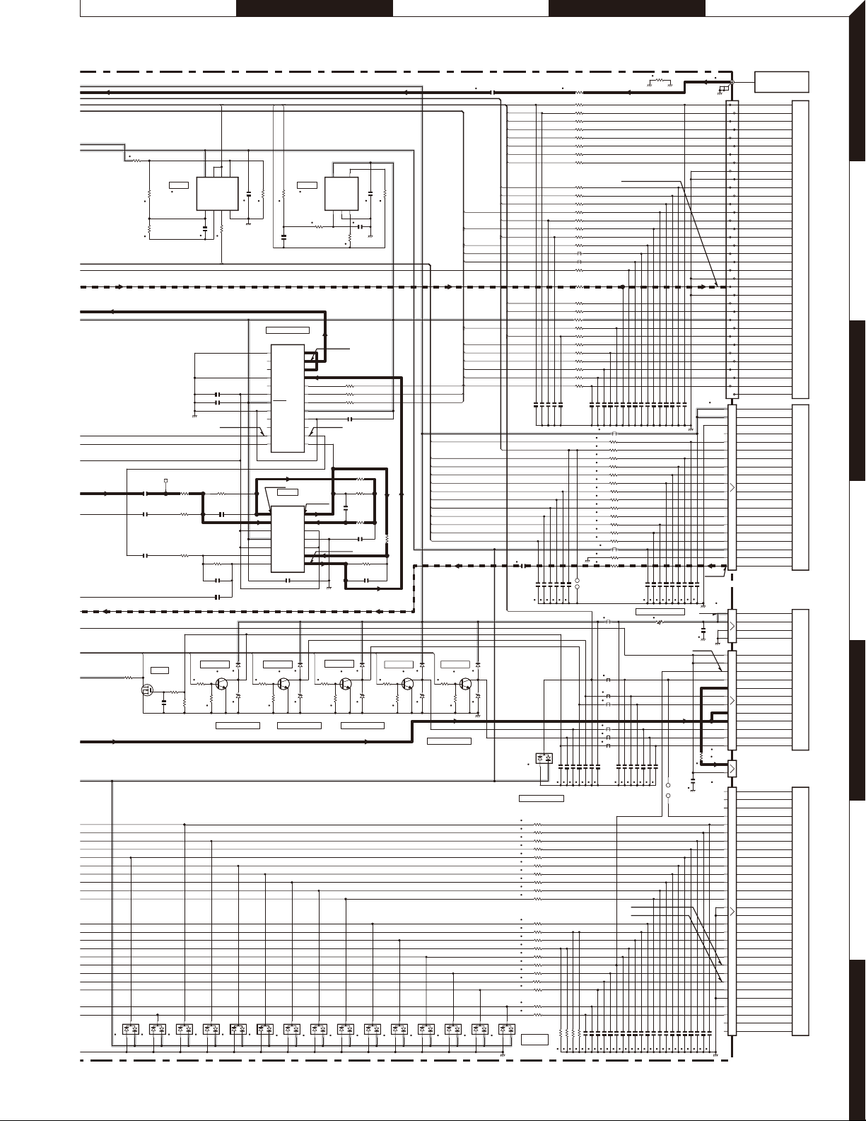
CONTROL UNIT (X53-4490-10)
SB
33M
50M
R163
330k
AF AMP
IC27
TC75W51FK(F)
R164
100k
R165
100k
SBC
MOD
33A
VREF
CN404
R445
C445
33k
1u
C446
R446
220k
0.1u
C450
R444
1u
33k
RA
DA204U
DC SW
Ao5
Q5
R190
0
R191
470k
C167
100p
D6
DA204U
SPo
33M_2
50M
oX_SDA
R186
SSM3K15TE(F)
10k
D4
D5
DA204U
VLi
5
6
7
8
IN-B
VDD
oUTB
oUTA2IN-A3IN+A4VSS
1
R166
100k
C138
100p
VLi_DiS
C459 220p
C460 0.1u
A
98mVrms 290mVrms
R451
100k
C455
100p
R452
47k
C456
220p
C457
1u
BUFFER AMP
Q6
2SD2114K(W)
R194
10k
10k
R196
SURGE PROTECTOR
D8
D7
DA204U
IN+B
D12,13
DA204U
D12
D13
C140
Ao1
1SS355
02DZ18F-X
D9
0.1u
R170
120k
DC/AC CONVERTER
13
14
15
16
17
18
19
20
21
22
23
24
564mVrms
1
2
3
4
5
6
7
BUFFER AMP
R197
10k
DA204U
RAMP
RAMP_TX
R172
C148
M62364FP-F
VIN5
VoUT5
VoUT6
VIN6
D0
VDAREF
RESET
GND
VIN7
VoUT7
VoUT8
VIN8
OP AMP
NJM2734V
AoUTPUT
A-INPUT
A+INPUT
V+
B+INPUT
B-INPUT
BoUTPUT
C461 0.1u
2SD2114K(W)
10k
R199
SURGE PROTECTOR
D10
IC412
IC411
DoUTPUT
D-INPUT
D+INPUT
C+INPUT
C-INPUT
CoUTPUT
Q7
DA204U
AF AMP
TC75S51FE(F)
10k
1200p
VIN4
VoUT4
VoUT3
VIN3
DI
CLK
LD
VDD
VIN2
VoUT2
VoUT1
VIN1
GND
D23
D24
D23,24
IC28
12
11
10
9
8
7
6
5
4
3
2
1
564mVrms
14
13
12
11
10
9
8
1SS355
02DZ18F-X
D11
DA204U
Ao2
R175
68k
BUFFER AMP
R204
10k
5
VDD
IN+2VSS3IN-
1
187mVrms
R460 100
R458 100
R459 100
C462 0.1u
C463
564mVrms
A
Q8
2SD2114K(W)
10k
R226
SURGE PROTECTOR
D14
DA204U
SCHEMATIC DIAGRAM
C166 0.01u R268 0
TMP1
TMP2
RAMP
FWD
TXASSiST
DA204U
D35
D36
1SS355
02DZ18F-X
D26
DA204U
RXASSiST
TX_CV
RX_CV
TXVCoB
RXVCoA/B
TXVCoA
LDT
LDR
RSSi
AGC
HWV1
/PSW
C466
1u
EXT_RSSi
SURGE PROTECTOR
SURGE
PROTECTOR
50M
4
oUT
0
R184
C158
0.1u
C156
220p
A
0
R179
R461
22k
R462
22k
330p
R463
22k
C465
R465
100k
1500p
R464
100k
C464
100p
Ao3
BUFFER AMP
D29,30
D29
1SS355
D30
02DZ18F-X
D15
DA204U
R254
10k
D16
DA204U
Q9
2SD2114K(W)
10k
R263
D31
D32
D18
DA204U
SPSD1
SPSCLK1
/EVDSCS_EV
SB
SPSD1_DiS
SR_STR_DiS
SPSCLK1_DiS
SR_oE_DiS
TXD2_DiS
/KEYi0
RXD2_DiS
/KEYi1
/KEYi2
KEYo0
KEYo1
VLi_DiS
Ao4
BUFFER AMP
Q10
1SS355
2SD2114K(W)
R267
10k
R269
02DZ18F-X
D31,32,35,36
SURGE PROTECTOR
D20
DA204U
10k
/RXPCS_TR
/16_8PCS
/TXPCS
SPSCLK0
SPSD0
/EWP
i2CCK
SPSCLK1
i2CDA
SPSD1
/ioCS
/EVCS
D22
C170 1000p
D28
DA204U
R209 120
R222
R210 1k
R211
R212
R213
R214
R215
R224 120
R225
R216 1k
R217 1k
R223 1k
R218 1k
R219 1k
R220 470
R205 1k
R206 1k
R207 1k
R208 1k
R221 1k
D4-11,14-16,
18,20,22,26
C184 1000p
R255 0
R256 0
R257 0
R258 0
R259 0
R260 0
R261 0
R262 0
R232 0
R233 0
R234 0
R253 0
R235
R236
R237
R238
R241 0
R242 0
R243
R244
R231
R245
R246
R247
R248
R249
R250
R251
R252 0
1000p
1000p
C176 1000p
C175
C179 1000p
C171
C190 100p
C188 100p
C186 100p
C193 100p
C182 1000p
C180 1000p
D28
100
100
100
1k
1k
1k
1k
1.2k
R228
R227 1.2k
C196 1000p
ADACABAAZ
NXR-710
R502
0
MIC&TA
W:257mVrms
N:129mVrms TD:69mVrms
0
0
0
0
L22
L23
0
0
0
0
0
0
0
0
0
0
1000p
1000p
100p
C185 1000p
R229 1.2k
C187 1000p
R230 1.2k
100p
1000p
100p
100p
100p
C202 100p
C221
C218
C211
C200
C198
C206
L317
R270 100
R271 100
R272 100
R273 100
R274 100
R275 100
R276 470
R277 100
R278 470
R279 470
R265
470
R266 470
R280 100
L17
R466 0
A
R467 0
CN45
CN46
L8
L9
L10
L11
L14
L15
L16
C191 1000p
C209 1000p
C189 1000p
C192 0.01u
C195 1000p
C194 1000p
C197 1000p
C215 1000p
C212 1000p
C203 1000p
C199 0.01u
C205 1000p
C201 1000p
C207 0.01u
100p
C233 100p
C224
C227 100p
C230
C240 1000p
C243 100p
CURRENT PROTECTOR
D37
SMD185F-2
C222 1000p
C228 1000p
C219 1000p
C225 1000p
80mVrms
400mVrms
C213 0.01u
C220 1000p
C216 1000p
C210 1000p
100p
C237
C246 100p
C223 1000p
C241
C250 100p
C226 1000p
1000p
C244
C252 1000p
C229 1000p
CN36
CN37
C247 1000p
C254 100p
C232 1000p
C257 1000p
C256 100p
C235 0.01u
C258 100p
80mVrms
C472
C239 100p
C259 0.1u
C242 1000p
R281
0.01u
13.6V
C473
40mVrms
A
C245 100p
CN38
CN40
0.01u
CN42
CN43
5.6
CN44
C249 1000p
CN39 iF_SiG
A
1
2
3
4
5
6
7
8
9
10
11
12
13
14
15
16
17
18
19
CN41
1
2
1
2
30
29
28
27
26
25
24
23
22
21
20
19
18
17
16
15
14
13
12
11
10
9
8
7
6
5
4
3
2
1
(X57-7940-10)-CN802
TMP11
TMP22
RAMP3
FWD4
TXASSiST5
RXASSiST6
TX_CV7
RX_CV8
GND9
GND10
TXVCoB11
RXVCoA/B12
TXVCoA13
/RXPCS_TR14
LDT15
/16_8PCS16
LDR17
/TXPCS18
SPSCLK019
SPSD020
SBC21
GND22
MoD23
GND24
RSSi25
AGC26
33A27
/EWP28
HWV129
i2CCK30
SPSCLK131
i2CDA32
SPSD133
/ioCS34
/EVCS35
NC36
SB
SB
GND
NC
DAT
PSW
STB1
CLK
SoE
TXD1
K1
RXD1
K2
K3
K4
K5
VLi
5C
MiG
MiC20
SB
SB
GND3
GND4
SPG12
SPG11
RD10
RSi9
SPi8
Ao17
Ao26
SPo5
SPo4
Ao33
Ao42
Ao51
SPo
SP
SPG
NC
NC
NC
NC(RSSi)
BER_CLK_D25
RXD0_D25
EXT_MoN_D25
TXD0_D25
/EPTT_D25
Ai1_D25
SC_D25
Ai2_D25
BER_DATA_D25
Ai3_D25
TXG
DG
io1_D25
TD_D25
io2_D25
TA_D25
io3_D25
RD_D25
io4_D25
RA_D25
io5_D25
RXG
io6_D25
SPM_D25
NC
NC
TX-RX UNIT
1
2
TX-RX UNIT (X57-7940-10)-CN800
3
4
TEST/SPKRD-SUB CONTROL I/O DISPLAY UNIT (X54-3580-20)-CN502
5
6
7
Note : The components marked with a dot (•) are parts of layer 1.
85
X53-449 6/6
Page 86

A B C D E
NXR-710
DISPLAY UNIT (X54-3580-20) (A/2)
1
KEY3
820
1/2W
R521
S501
100p
C513
2
DC SW DC SW
Q512 Q513
UPA672T-A UPA672T-A
3
4
C514
R522
100p
820
KEY2
1/2W
SCHEMATIC DIAGRAM
C515
C512
9
QS
10
Q’S
11
Q8
12
Q7
13
Q6
14
Q5
15
OE
16
VDD
BU4094BCFV
R523
100p
IC503
820
0.01u
VSS
CLK
DATA
STRB
KEY5
KEY1
1/2W
S503
C516
8
7
Q4
6
Q3
5
Q2
4
Q1
3
2
1
SHIFT
REGISTER
R524
100p
820
KEY3
1/2W
S504S502
DC SW
Q514
UPA672T-A
C517
R606
R525
100p
820
1/2W
47k
KEY2
S505
C518
R534
KEY1
1/2W
KEY4
S506
PF6PF5PF4PF3PF2PF1
820
R526
100p
CP501
470*4
DC SW
Q517
UPA672T-A
Q516
UPA672T-A
DC SW
D506
LA-501DD
10
1
56
7SEGMENT
C519 0.01u
SHIFT
REGISTER
9
VSS
QS
10
Q’S
Q8
Q7
Q6
Q5
CLK
OE
DATA
VDD
STRB
IC504
BU4094BCFV
Q4
Q3
Q2
Q1
11
12
13
14
15
16
8
7
6
5
4
3
2
1
CLK
SOE
D512
DA204U
D512,513,514
SURGE
ABSORPTION
D513
DA204U
D514
DA204U
BUSYC
C511 0.01u
IC502
DATA
STRB
8
VSS
7
Q4
6
Q3
5
R539
Q2
4
R540 1k
Q1
3
CLK
2
1
SHIFT
REGISTER
1k
R535
1k
R536
1k
POWLEDC
R538
1k
1k
R537
9
QS
10
Q’S
11
Q8
12
Q7
13
Q6
14
Q5
15
OE
16
VDD
1k
BU4094BCFV
5
DISPLAY UNIT (X54-3580-20) (B/2)
6
0.1u
C607
A
MIC5MIC GND
PTT/TXD
GND2SB1NC
6
4
3
7
J601
E58-0522-05
86
X54-358 1/2
8NC7 HOOK/RXD
C601
100p
R601
R6041k1k
R605
680
C602
1000p
CURRENT
PROTECTOR
MINISMDC020F
A A
2SK1824-A
D603
D601
DA204U
D601,602
SURGE ABSORPTION
Q525
D602
DA204U
D508
DA204U
VR601
10k
100p
C603
100p
C606
1
2
3
4
5
6
7
8
9
10
11
A
D509
DA204U
D508-511
SURGE ABSORPTION
CN601 CN501
VLI
5M
GND
NC
SB
NC
GND
PTT
MIG
MIC
HK
D510
DA204U
11
10
9
8
7
6
5
4
3
2
1
DA204U
R502
0
R503
0
D511
C501
10u10
PTT
MIC
MIG
DAT
HK
5M
VLI
SB
Page 87

DISPLAY UNIT (X54-3580-20) (A/2)
SCHEMATIC DIAGRAM
NXR-710
JIHGF
1
CLK
SOE
BUSYC
POWLEDC
Q518
UPA672T-A
DC SW
Q519
UPA672T-A
DC SW
CP502
470*4
DC SW
Q503
UPA672T-A
DC SW
Q504
UPA672T-A
CP503
470*4
UPA672T-A
DC SW
Q522
UPA672T-A
RT1P141M-T111
DC SW
Q521
DC SW
Q506
D507
LA-501DD
1
5
7SEGMENT
C520 0.01u
SHIFT
REGISTER
9
VSS
QS
10
Q’S
11
Q8
12
Q7
13
Q6
14
CLK
Q5
15
DATA
OE
16
STRB
VDD
IC505
BU4094BCFV
DC SW
Q508
RT1P141M-T111
10
6
8
7
Q4
6
Q3
5
Q2
4
Q1
3
2
1
R516
1k
1/2W
R517
820
1/2W
R518
1k
1/2W
CP504
470*4
DC SW
D503
B30-2151-05
LED
D504
B30-2151-05
LED
TX
CALL
BUSY
DC SW
Q523
Q524
UPA672T-A
UPA672T-A
VOLTAGE REGULATOR
C522
C521
10u10
VOLTAGE REGULATOR
C525
C524
10u10
TA78L05FF
1
oUT
0.1u
TA78L05FF
1
oUT
0.1u
IC506
CoM
2
IC507
CoM
2
3
IN
C523
0.33u
3
IN
C526
0.33u
3
4
S507
2
DAT
PTT
HK
5M
VLI
SB
MIC
MIG
R541
10k
R542
10k
VR501
10k
R505
R543
68k
R506
10k
10k
R544
10k
Q507
UPA672T-A
DC SW
Q501
2SC4116(Y)F
R508
1k
LEVEL
CONTROLLER
Q502
2SA1586(Y,GR)F
R507
6.8k
LEVEL
CONTROLLER
C502
C503
1.5u10
1.5u10
DC SW
Q510
RT1P141M-T111
D501
HSM88AS-E
AF DETECTOR
D502
HSM88AS-E
AF DETECTOR
C504
0.1u
C505
0.1u
Q509
RT1P141M-T111
DC SW
Q511
RT1P141M-T111
DC SW
47p
R510
C506
10k
R509
R511
0.1u
C507
R519
1k
1/2W
R520
820
1/2W
1
220k
AoUT
2
A-IN
3
A+IN
4
V-
NJM4558E-ZB
10k
C508
0.1u
BoUT
B-IN
B+IN
IC501
MIC AMP
MAIN DC
BACKUP
D505
B30-2151-05
LED
8
V+
7
6
5
C509
0.01u
C510
10u10
R512
R513
R514
10k
100k
150k
KEY1
KEY3
KEY2
KEY5
KEY4
13.10V
R529 1k
R530 1k
R531 1k
R532 1k
R533 1k
CN502
20
SB
19
SB
18
NC
17
GND
16
PSW
15
DAT
14
CLK
13
STB1
12
PTT/TXD
11
SOE
10
HK/RXD
9
K1
8
K3
7
K2
6
K5
5
K4
4
5C
3
VLI
2
MIC
1
MIG
CONTROL UNIT
5
(X53-4490-10)-CN40
6
7
Note : The components marked with a dot (•) are parts of layer 1.
87
X54-358 2/2
Page 88

A B C D E
NXR-710
TX-RX UNIT (X57-7940-10)
1
CONTROL UNIT
(X53-4490-10)
-CN301
FINAL UNIT
(X45-3920-10)
(A/3)-CN203
2
3
4
GND
GND
EXT_IN
CN700
3
SB
2
+B
1
13.6V 7.93V
3
+B
2
+B
1
CN701
EXT Ref:10MHz/0dBm
CN500
13.54V
13.6V
C701
C700
SCHEMATIC DIAGRAM
VOLTAGE
47u35
80C
80C
80C
0.01u
10MHz-->
F700
R700
5A
33
RT1N141M-T111
C702
NJM78M05DL1AZB
C703
1000p
2SJ506-E(S)
R705
100k
DC SW
Q703
DC/DC CONVERTER 15V
7.65V
R701
10
1u
VOLTAGE
REGULATOR
IC700
1
IN3oUT
GND
2
DC SW
Q702
R706
1k
C704
C709
0.01u
R703
0
1u
5.08V
C705
1000p
C711
DC SW
L700
C706
C707
1000p
68u
4.7u16
10u35
REGULATOR
NJM78M08FA-ZB
1
IN3oUT
Q704
SSM5H01TU-F
R707
150k
0.1u
C708
SSM3K15TE(F)
SSM3K15TE(F)
IC702
GND
2
1
2
3
4
R702
DC SW
DC SW
R708
DC SW
Q706
Q701
150C
VOLTAGE
REGULATOR
IC701
XC9101D09AKR
EXT
LSEN
VoUT/FB
VIN
CC/GAIN
CE/SS5CLK
DC SW
Q700
CPH3317
47k
R704
Q705
CPH3317
47k
R710
TX VCO/PLL (E23-1278-05)
CN807
CN808
C716
C713
10u35
1000p
14.51V
1u
1u
22p
C717
8
VSS
7
6
C715 1000p
R711 12k
C714 180p
7.92V
4.7k
5.06V
1000p
1u
C722
R709
0.1u
C723
0.1u
47k
VOLTAGE REGULATOR
TK11230CMCL-G
1
VCoNT
2
GND1
3
NoISEPASS
TK71733S
1
VIN
2
GND
3
oN/oFF
VOLTAGE REGULATOR
C718
4.7k
R712
470k
C712
C710
1000p
R713
R714
IC704
IC703
NP/VREF
330k
22k
GND2
VoUT
VoUT
C721
C719
6
VIN
5
4
5
4
C720
CN809
C724
0.1u
R715
RX VCO/PLL
(E23-1278-05)
CN811
CN812
L701
R716
10u
0
0
1u
C727
C725
3.01V
1u
3.27V
1u
R717
L702
10u
0
C728
C726
1000p
0.01u
C729
1000p
CN813
150C_1
150C_2
RXC
R860
0
R861
0
80C
SBC
80R
50C
50R
30R
33C
10MHz-->
TMP1
36
35
34
33
32
31
30
29
28
27
26
25
24
23
22
21
20
19
18
17
15
16
14
13
12
11
10
9
8
7
6
5
4
3
2
1
CN800
CN801
11GND
108TC
9RAMP
8ASWC
7FA N
6FDT
5TMP2
4TMP1
3
2H/L
1
CN802
R800 0
R850 0
R801 0
R802 0
R803 0
L805
L806
R806 0
R807 0
R808 0
R809 0
R810 0
R811 0
R812 0
R813 0
R814 0
R815 0
R851 0
140mVrms
<-- 450kHz
TXASSIST
RXASSIST
TX_CV
RX_CV
D801
CN803
LDR
450kHz
CN804
DC SW
D801
1SS388F
ASWC
CN805
TXVCOB
RXVCOA/B
TXVCOA
/RXPCS_TR
/16_8PCS
/TXPCS
SPSCLK0
SPSD0
RSSI
C818
R816
R817
5.08V
0.1u
100
100
C820
TEMPERATURE SENSOR
IC800
LM73CIMKX-0
4
VDD
SMBCLK
5
GND
ALERT
6
SMBDAT
ADDR
22
R829
5.07V
C823
0.1u
1000p
10p
220k
R828
C822
R827
10k
3
2
1
8
7
6
5
LDT
LDR
SBC
8TC
MOD
CN806
50C
R818
R820
R819
68k
1k
C814
47k
100p
OP AMP
TC75S51FE(F)
1
IN+
2
VSS
3
IN-4oUT
R821
390k
IC801
5
VDD
Q800
SSM3K15TE(F)
3.28V
C815
0.01u
R830
330k
IC803
TC75W51FK(F)
oUTA
VDD
oUTB
IN-B
IN+B
BUFFER AMP
R831
56k
IN+A
R822
C817
IN-A
VSS
DC SW
100k
L803
0.1u
R826
C819
R832
68k
1
2
3
4
TMP2
RAMP
FWD
TXASSIST
RXASSIST
TX_CV
RX_CV
GND
GND
TXVCOB
RXVCOA/B
TXVCOA
/RXPCS_TR
5
CONTROL UNIT
(X53-4490-10)-CN38
/16_8PCS
/TXPCS
SPSCLK0
SPSD0
GND
MOD
GND
RSSI
/EWP
HWV1
I2CCK
SPSCLK1
I2CDA
SPSD1
/IOCS
/EVCS
LDT
LDR
SBC
AGC
33A
NC
6
FINAL UNIT
(X45-3920-10)(A/3)-CN204
CONTROL UNIT
(X53-4490-10)
7
-CN39
PLIM
HWV2
5.6k
0.01u
R824
R825
100
100
C821
M24C02-RMN6TP
5
SDA
6
SCL
7
WC
8
VCC
3.28V
0.1u
ANALOG SW
TC7W53FK(F)
4
GND5A
3
VEE
2
INH
1
CoMMoN
EEPROM
IC802
IC806
4
VSS
3
E2
2
E1
1
E0
33A
/EWP
SPSCLK1
SPSD1
/IOCS
/EVCS
6
CH1
7
R853
CH0
8
0
VCC
C831
0.1u
3.27V
33C
MOD -->
AGC
ASWC
FAN
PLIM
<-- 450kHz
88
X57-794 1/8
Page 89

TX-RX UNIT (X57-7940-10)
50C
R500
C500
0.1u
50C
33C
R501
10MHz-->
R502
DC SW
Q500
SSM6L05FU-F
100k
INT Ref:0V
EXT Ref:4.94V
INT Ref:0V
EXT Ref:2.81V
C501
0.1u
D500
UDZS3.0B
D501
UDZS3.0B
100k
100k
C502
LIMITER
LIMITER
1
0.1u
2
SCHEMATIC DIAGRAM
50ER
INT Ref:0V
EXT Ref:5.04V
C520
0.1u
R520
22
22k
470
R514
R515
C514
R516
22
3.25V
2.7k
C519
Q502
2SK3737-5
RF AMP
0.68V
R518
0.01u
390k
0
C515
3SK294-FP
0.01u
C517
0.01u
1k
C503
0.1u
22
R504
R505
120k
R503
100
INT Ref:0V
EXT Ref:2.16V
L77-3034-05
VC
GND3oUTPUT
2SC4617(R)
R506
R507
OSC
X500
4
VCC
RSSIOFS --> RSSIOFS -->
C506
RF AMP
Q501
C507
0.1u
470
22
0.1u
3.25V
C504
1000p
C505
0.1u
C508
0.01u
C509
R509
0.1u
C510
0.1u
C511
0.1u
C512
0.1u
R510
22k
10MHz AMP
AMP
0V
18k
R511
R512
R513
R521
R522
RF AMP
Q503
150k
1
2
3
4
33k
0.1u
L500
C518
LPF
L501
4.7u
18p
C521
R524
100k
BUFFER AMP
IC500
TC75W51FK(F)
oUTA
VDD
oUTB
IN-A
IN+A
IN-B
VSS5IN+B
3.3u
INT Ref:0V
EXT Ref:G1:2.47V G2:2.27V
180
0.1u
R519
18p
R523
C524
10p
C551
C532
0.1u
8
R528
7
220k
6
100k
C531
R527
D:4.92V S:0.87V
R525
0
150
C530
0.1u
DETECTOR
D503
HSM88AS-E
0.1u
100k
R529
C534
C525
47p
L502
C522
680n
100p
C523
330p
C533
R531
2.30V
R530
470
R532
50ER
OP AMP
IC501
TC75S59F-F
3
IN+4oUT
2
VSS
1
VDD
IN-
R539
100k
R536
2.7k
Q505
SSM3K15TE(F)
R534
6.8k
DC SW
5p
C528
120p
L503
C544
0.1u
560n
C529
220p
C526
470p
LPF
0.1u
22
R533
4.90V
10k
2.2u
L504
2SC4617(R)
10k
C535
0.01u
R535
R537
RF AMP
Q504
R538
100k
1k
1.64V
220
DC SW
Q506
SSM6L05FU-F
0.1u
C536
C538
NXR-710
5
0.01u
C537
0.1u
C541 0.1u
C542 10u
R540
100k
C540
INT Ref:5.07V
EXT Ref:0.15V
R541
100
C543
82p
C539
R542
0.01u
0.1u
DC SW
Q507
UPA672T-A
100k
R544
100k
L507
33u
L505
1.2u
L506
1.2u
R543
R551
L508
C545
0.1u
R547
1.8k
12
R545
R548
1.8k
39p
220
C546
R549
1.8k
12
R546
R550
1.8k
100
C549
0.1u
33u
JDP4P02AT
C547
JDP4P02AT
C548
RF SW
D504
10p
RF SW
D505
10p
1dB ATT
1dB ATT
JIHGF
19.2MHz or 10MHz -->
C550
0.01u
1k
R552
MB -->
MO -->
33A
/EWP
SPSCLK1
SPSD1
/IOCS
/EVCS
MOD -->
AGC
ASWC
FAN
PLIM
<-- 450kHz
R833 100
R834 100
R835 100
DIGITAL
POTENTIOMETER
IC804
M62364FP-F
CN810
R837
0
8DI9
10
12
CLK
VIN3
VIN4
VoUT311VoUT4
VIN514VoUT515VoUT616VIN617D018VDAREF19RESET
13
C825
100u
EVOL
Vref
C826
4
5
6LD7
VDD
VIN2
GND21VIN722VoUT723VoUT824VIN8
20
CN814
MB -->
MO -->
1.64V
3.28V
R841
100
R838
100
L800
3.28V
1u
VT2 -->
VT1 -->
1
2
VIN1
VoUT13VoUT2
R855
0
3.28V
R840
VT2 -->
VT1 -->
20
SI
1
So
2
I/O EXPANDER
A1
3
A0
MCP23S08TE/ML
4
RESET
5
CS
100
NC_17INT8NC_29GP010GP1
6
L801
R845
100k
C828 0 .1u
C827 1 000p
R844
100k
16
18
19
15
GP717VSS
SCK
VDD
GP6
14
GP5
R842
100k
GP4
GP3
GP2
W_/N
VN_/N
R843
100k
13
12
11
R848 100k
R847 100k
R846 100k
R849 100k
ASWC
8TC
RXC
MB -->
MO -->
FAN
W_/N
VN_/N
<-- 450kHz
19.2MHz -->
19.2MHz -->
VT2 -->
VT1 -->
AGC
IC805
89
X57-794 2/8
Page 90
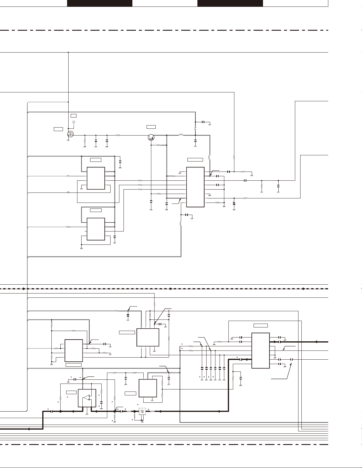
K L M N O
NXR-710
19.2MHz or 10MHz --> 19.2MHz or 10MHz -->
LDT
33C
SSM3K15TE(F)
33C
SPSCLK0
SPSD0
/16_8PCS
DC SW
Q600
L613
L614
R602
LDT
CN600
100
SCHEMATIC DIAGRAM
DC SW
R604
100k
TC7WH126FU-F
1
G1
2
A1
3
Y2
4
GND5A2
TC7WH126FU-F
1
G1
2
A1
3
Y2
4
GND5A2
C600
BUFFER
IC600
BUFFER
IC601
R683 0
R684 0
R685 0
Q601
2SA1832(GR)F
C604
R607
100k
R606
100k
0.1u
R605
0
10u
10u
C601
0.1u
C602
8
VCC
7
G2
6
Y1
8
VCC
7
G2
6
Y1
0.1u
C603
C605
R608
100k
0.01u
L601
10u
3.27V
L600
16.8MHz PLL
ADF4001BRUZ
9
DGND
10
CE
11
CLK
12
DATA
13
LE
14
MUXoUT
15
DVDD
16
VP
C606
10u
10u
IC602
L602
C607
CPGND
REFIN
AVDD
RFINA
RFINB
AGND
RSET
10u
C608
0.01u
CP
16.8MHz MOD PLL
L603
8
7
6
5
4
3
2
1
10u
3.26V
C611
0.01u
C612
0.01u
R609
TX-RX UNIT (X57-7940-10)
0
R610
C610
R611
0.01u
100
C613
0.01u
R613
C614
0
10u20
4.7k
R612
47
C615
180p
50C
MB --> MB -->
MO -->
RSSIOFS -->
50C
33C
R449
330k
R450
56k
IC409
TC75W51FK(F)
1
C400
0.1u
R448
R402
oUTA
2
IN-A
3
100
IN+A
4
VSS5IN+B
330k
BUFFER AMP
C403
0.1u
IF AMP
IC400
AD8051ART
R403
6.8k
RSSI
33C
AGC
W_/N
<-- 450kHz
19.2MHz -->
19.2MHz --> 19.2MHz -->
VT2 -->
VT1 -->
oUTB
VDD
IN-B
8
7
6
22
3.17V
R406
5
+VS
VoUT2-VS3+IN
1
3.27V
C440
R451
0.1u
R452
100k
220k
R400
220k
4
-IN
10k
R408
R409
C406
0.1u
R410
R401
22
BUFFER AMP
TC75W51FK(F)
47k
1.62V
C408
0.1u
47k
5.04V
C401
0.1u
IC401
R404
0.1u
C402
IC402
LMC7101BIM5
OP AMP
R415
0
8
VDD
oUTA2IN-A3IN+A4VSS
1
BUFF & DIFF AMP
0
4
CF400
L72-1028-05
R416
2.2k
7
INPUT+
INPUT-5V-
oUTB
2V+3
R407
6
R421
1.8k
R405
470k
5
IN-B
1
OUTPUT
IN+B
10k
C407
1000p
3.26V
R412
R413
50C
MO -->
3.27V
10p
C404
IF SYSTEM
IC403
NJM2287V
C418
14
1000p
Lo_DEC
C416
13
Lo_IN
0.01u
12
V+1
11
V+2
10
RSSI
9
C417
IF_oUT
8
0.1u
GC_IN
C415 0.1u
100
R422
C419
1000p
R417 22
R418 22
<-- RSSI
3.26V
3.17V
AGC -->
<-- 450kHz
47k
R411
R453
22
C405
0.1u
100
0
C410 1000p
R420
47
C412 1000p
C411 1u
C413 1u
C414 1000p
RF_DEC
RF_IN
GND1
MIX_oUT
GND2
IF_IN
IF_DEC
C421
1000p
1
2
3
C423
0.01u
4
5
C424
6
0.1u
7
C422
0.1u
AW:-72.2dBm
AN:-72.9dBm
VN:-75.6dBm
-88.4dBm
C425
0.1u
450kHz -->
19.2MHz -->
W_/N
VN_/NVN_/N
VT2 -->
VT1 -->
33C33C
90
X57-794 3/8
Page 91

TX-RX UNIT (X57-7940-10)
50C
C616
47p
L604
330n
Vref
Vref -->
CN601
MB
TSRQP
SCHEMATIC DIAGRAM
16.8MHz--> 16.8MHz-->
22
0.1u
220p
1.16V
47u10
C627
0.01u
100
R618
Q602
2SC4617(R)
RF AMP
R619
22k
R614
C621
47u10
R621
1u
10k
R622
L606
4.94V
1.70V
R626
C630
R625
0.01u
220
5.6k
R623
220
C629
0.01u
R615
27k
R616
R617
100k
C626
10k
10u20
R620
0
C628
1
2
10p
3
4.7k
2.37V
C633
0.01u
OP AMP
IC603
TC75S51FE(F)
IN+
VSS
IN-4oUT
C631
10p
R624
220k
R627
R628
VDD
C634
22
4.96V
R630
Q603
2SC4617(R)
RF AMP
470
5
0.01u
100k
3.02V
C632
C636
0.01u
3.26V
0.1u
C637
R629
100k
0.01u
R631
C635
<--16.8MHz
R632
1.8k
8.2k
10p
C641
0.01u
C639
0.01u
OP AMP
IC604
LMC7101BIM5
C643
3.27V
10u20
R635
R633
2V+3INPUT+4 INPUT-
3
4
2.2
22
1
5
oUTPUT
VCC
C642
0.1u
V-
OSC
X600
L77-1960-15
OUTPUT
GND
MB_CV2
CN602
1.48V
2
1k
R640
1
VC
0
R639
10p
R636
100k
C644
C625
0.01u
C624
LPF
C620
18p
L605
C623
390n
0.01u
C619
330p
C622
C618
NXR-710
R650
C653
1k
10u20
R651
7.91V
1k
DC SW
Q605
2SC5383-T111
C654
10u20
C655
1000p
C656
10u35
7.93V 7.27V
R649
0
C658
1000p
33C
TXVCOB
80C_1
TXVCOA
80C
R634
47k
C638
MB -->
MO -->
450kHz --> 450kHz -->
R425
18k
IF AMP
IC404
MCP6021-E/OT
33C 33C
W_/N
VN_/N
19.2MHz -->
19.2MHz -->
VT2 -->
VT1 -->
5
VDD
VoUT2VSS3VIN+
1
4
VIN-
R426
C426
C427
0.1u
8.2k
47k
R427
0.1u
C428
0.1u
47k
R428
AW:-98.4dBm
AN:-99.0dBm
VN:-100.2dBm
R637
47k
OP AMP
IC605
TC75S51FE(F)
1
IN+
VDD
2
1u
VSS
3
IN-4oUT
R429
22
R431
3.25V
0
ANALOG SW
IC405
TC7W53FK(F)
1
CoMMoN
2
INH
3
VEE
4
GND5A
ANALOG SW
IC406
TC7W53FK(F)
1
CoMMoN
2
INH
3
VEE
4
GND5A
22
R638
5
3.27V
1u
C645
Vref -->
33C
C429
0.1u
W_/N
3.27V
8
VCC
7
CH0
6
CH1
C430
0.1u
8
VCC
7
CH0
6
CH1
W_/N
VN_/N
VN_/N
NARROW
VERY NARROW
R433
WIDE
R434
R435
MO
CN603
1.63V
R642
100k
OP AMP
IC606
0
LMC7101BIM5
R641
Vref
W:3.28V
N:0V
VN:0V
CF401
L72-1028-05
0
R436
1.5k
W:3.28V
N:0V
VN:3.28V
CF402
L72-1027-05
0
0
R437
R438
1.5k
CF403
L72-1041-05
1.5k
100k
R643
R442
R443
R444
1.2k
4
820
820
R645
2V+3
INPUT+
INPUT-5V-
22
C649
0.1u
1
OUTPUT
C437
R648
C438
0.1u
0.1u
270k
ANALOG SW
TC7W53FK(F)
5
A
6
CH1
7
CH0
8
VCC
ANALOG SW
TC7W53FK(F)
5
A
6
CH1
7
CH0
8
VCC
C652
10p
IC407
CoMMoN
IC408
CoMMoN
GND
GND
33C
4
3
VEE
2
INH
1
R447
C439
0
0.1u
4
3
VEE
2
INH
1
19.2MHz -->
19.2MHz -->
VT2 -->
VT1 -->
91
X57-794 4/8
Page 92

U V W X Y
NXR-710
SUB UNIT (TX VCO/PLL) (X58-5080-10) (B/2)
Q350
SSM6L05FU-F
R350
470k
DC SW
DC SW
Q351
SSM6L05FU-F
R351
470k
CN350
1
1
TXVCOB
80C_1
TXVCOA
TX_CV
TXASSIST
GND
MO
GND
2
2
TXVCOB
3
3
80C_1
4
4
TXVCOA
5
5
TX_CV
6
6
MO
7
7
TXASSIST
R353
R355
0
10k
SUB UNIT (TX VCO/PLL) (X58-5080-10) (A/2)
TX_CV
SCHEMATIC DIAGRAM
R361
R354
470k
VCOA:3.30V
VCOB:0V
R373
470k
VCOA:0V
VCOB:3.30V
33
R356
C333
0.01u
C350
0.1u
R327
D352,355,358,359
FREQUENCY
R357
0
0
R301
390
0.047u35
C306
CONTROL
L350
10u
5p
C382
L365
L351
10u
5p
C384
C357
1000p
C311
1000p
R303
0
C303
10u20
150
R302
C308
0.01u
C309
0.01u
C310
10p
0.01u
3.25V
D355
C354
1000p
1SV282-F
10u
L352
L354
D352
2.2u
1SV282-F
C356
1000p
D357
C355
1SV282-F
1000p
10u
L353
L355
D353
2.2u
1SV282-F
D353,357,360,361
FREQUENCY CONTROL
56
6.8n
L307
R307
C312
R305
0
5.08V
3.21V
C307
0.15u35
6
CPout1
7
NC
8
/OSC_AC_GND
9
OSC
10
OSCout
11
VCC_SOC
12
GND_OSC
LD/PS214VCCcp215CPout216/Fvco17Fvco18VCCcp2
13
10
R306
3.26V
L305
0
R379
3V
R358
L366
0.1u
C379
R325
0
R331
0
L300
C300
L303
1.2u
0
10p
C304
C358
0.01u
D358
D359
C359
D360
D361
C323
3p
33p
4
5
LD/PS1
VCCcp1
PLL
IC300
SKY72300-362
L306
C360
1SV282-F
L356
1SV282-F
C361
0.01u
1SV282-F
L357
1SV282-F
4.94V
L309
68n
2
3
/Fin
33
1000p
C362
22p
10u
R362
1000p
C363
22p
10u
R312
47
C328
Fin
VCC_digital
33
1
VCC
Max_out
Mod_in
Clock
C366
33p
GND
Data
1000p
67n
L358
C367
1000p
50n
L359
C329
C330
6.8n
L314
25
24
23
22
21
/CS
20
19
15p
C372
2p
C368
15p
C373
3p
C369
1000p
R318
5p
2SC5636
BUFFER AMP
R308 10
R310 1k
C314 1u25
C315 100p
C316 100p
C317 0.01u
C318 100p
R311 10
C313
3.21V
C320 100p
C321 100p
100p
2.2k
Q300
R319
C322
VCOA:7.07V
VCOB:0V
V-TXVCO A
VCO OSC
Q352
MCH3914(8)-H
L362
VCOA:0V
VCOB:7.07V
V-TXVCO B
VCO OSC
Q353
MCH3914(8)-H
47n
L315
330
C331
1000p
C324
100p
R363
100p
TX-RX UNIT (X57-7940-10)
33
10k
C332
5.6k
1000p
1p
47
47
1p
10u
330
47k
R368
10k
R369
R322
8.2
C326 100p
R313 47k
R315
R316
R317 100
C335 100p
L364
C377
L310
7.05V
68n
680
R371
C378
12p
Q354
2SC5636
BUFFER AMP
220
R370
1000p
R324
8.2
150
R323
100
10
R374
R377
0
0
R372
0
SPSCLK0
/TXPCS
SPSD0
R333
L607
2
1
1
2
3
4
5
6
7
8
GND
Vo
L618
FIN
SPSCLK0
/TXPCS
SPSD0
33C
50C
LDT
REF
3.27V
5.07V
47n
100
C664
R666
0.01u
C663
L615
L616
SPSCLK0
/TXPCS
SPSD0
33C
50C
39p(G)
L608
47n
39p
C662
1.0u
R663 0
CN351
2
GND
Vo
1
CN303
1
FIN
2
3
4
5
33C
50C
6
7
LDT
8
REF
0
R367
C376
10u
C374
330
R365
R366
C375
L363
R364
R320
1000p
R321
L312
L313
16.8MHz--> 16.8MHz-->
DC SW
Q604
2SC5383-T111
1000p
150C_2
R644
C647
10k
2.2u35
C648
19.2MHz -->
19.2MHz -->
VT2 -->
VT1 -->
C688
92
X57-794 5/8, X58-508 (A,B/2) 1/1
14.46V
2.2u35
TXASSIST
R646
R647
R658
CN604
TX_AST
13.87V14.50V
0
C650
1000p
1k
C651
100p
OP AMP
IC607
LMC7101BIM5
1
OUTPUT
2
V+
3
INPUT+4INPUT-
TX ASSIST
R652
5
V-
R653
R654
1k
120k
33k
C657
DC SW
D600
DA221
R656
33p
10M
R655
390k
50C
10k
22k
R657
TC75W51FK(F)
5
IC608
AF AMP
IN+B
CN606
TX_CV
C660
10p
R659
220k
6
7
8
IN-B
VDD
oUTB
oUTA2IN-A3IN+A4VSS
1
TX_CV
R660
R661
330k
39k
C661
0.1u
5.07V
R665
0
50C
19.2MHz -->
19.2MHz -->
VT2 -->
VT1 -->
Page 93
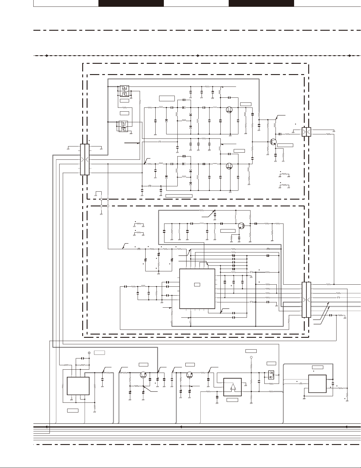
TX-RX UNIT (X57-7940-10)
GND
NC
80C_2
RXVCOA/B
RX_CV
NC
RXASSIST
SUB UNIT (RX VCO/PLL) (X58-5070-10) (B/2)
Q350
SSM6L05FU-F
R350
470k
DC SW
R352
0
DC SW
Q351
SSM6L05FU-F
R351
470k
CN350
GND
1
1
NC
2
2
80C_2
3
3
RXVCOA/B
4
4
RX_CV
5
5
NC
6
6
RXASSIST
7
7
VCOA:3.3V
VCOB:0V
SUB UNIT (RX VCO/PLL) (X58-5070-10) (A/2)
3V
RX_CV
C333
R327
0.01u
R354
470k
0
R325
R331
L300
C304
ADACABAAZ
SCHEMATIC DIAGRAM
33
C328
C364
C367
C365
12345
Max_out
Mod_in
18
18p
VCC
GND
Clock
Data
VCCcp2
C366
/CS
L358
50n
7p
1000p
L359
50n
5p
L314
1000p
25
24
23
22
21
20
19
L360
L361
C329
4p(B)
6.8n
C368
C369
C330
VCOA:6.94V
VCOB:0V
10u
C370
8p
Q352
MCH3914(8)-H
15p
VCOA:0V
VCOB:6.94V
10u
C371
8p
Q353
MCH3914(8)-H
12p
1000p
2SC5636
BUFFER AMP
R308 10
R310 1k
C314 1u25
C315 100p
C316 100p
C317 0.01u
C318 100p
R311 10
C313
100p
3.24V
C320 100p
C321 100p
Q300
R319
VCO OSC
L315
330
C322
C372
Q353
C373
100p
27n
C331
Q352
VCO OSC
L362
8p
R363
8p
1000p
C324
100p
L363
R364
10u
L312
L313
270
R320
R321
C374
R365
R366
C375
1p
R367
47
C376
47
1p
10u
270
22k
C332
10p
10k
R361
D352,355,358,359
FREQUENCY
CONTROL
0
R379
C379
0
0
L303
10p
L350
R357
0
3V
R358
0
L366
0.1u
R301
390
C300
0.047u35
1.2u
C306
C353
C352
10p
R304
10u
100p
D352
L365
L351
10u
100p
D353
C357
1000p
FREQUENCY CONTROL
C311
R303
0
C303
10u20
150
R302
C308
0.01u
C309
0.01u
C310
4.7k
0.01u
3.27V
C354
1000p
1SV325F
C355
1000p
1SV325F
D353,357,360,361
R307
1000p
C307
R306
L305
L352
C356
L353
47
R305
0.1u35
10
11
12
10
1SV282-F
10u
1000p
1SV282-F
10u
L307
0
5.07V
3.24V
7
8
9
OSC
OSCout
C358
C380
3p
D355
D358
L354
10u
D359
C359
C381
3p
D357
D360
L355
10u
D361
C323
3p(B)
18p
6.8n
C312
6
CPout1
VCCcp1
NC
/OSC_AC_GND
SKY72300-362
VCC_SOC
GND_OSC
LD/PS2
VCCcp2
1314151617
3.29V
L306
0.01u
1SV282-F
L356
1SV282-F
C361
0.01u
1SV282-F
L357
1SV282-F
LD/PS1
PLL
IC300
CPout2
R312
L309
C360
33
39n
/Fin
/Fvco
VCO A
C362
33p
10u
R362
33
1000p
VCO B
C363
22p
10u
4.94V
1000p
Fin
VCC_digital
Fvco
NXR-710
7.09V
33
R368
1000p
R369
R322
8.2
L310
C326 100p
R313 10k
R314 4.7k
R315 100
R316 10
R317 100
C335 100p
47k
10k
R323
L364
82n
C378
10p
2SC5636
BUFFER AMP
C377
1000p
R324
8.2
150
R372
Q354
R370
R374
0
R377
0
/RXPCS_TR
0
220
SPSCLK0
SPSD0
R333
CN351
GND
2
Vo
1
CN303
FIN
1
2
3
4
33C
5
50C
6
LDR
7
REF
8
0
2
1
1
FIN
2
SPSCLK0
3
/RXPCS_TR
4
SPSD0
5
33C
6
50C
7
LDR
8
REF
3.27V
5.07V
GND
Vo
R247
R248
18
18
C212
0.01u
R217 0
L213
R220
100
19.2MHz -->
VT2 -->
VT1 -->
RXVCOA/B
19.2MHz -->
R202
10k
22k
R200
TC75W51FK(F)
5
IN+B
IC200
OP AMP
19.2MHz -->
DC SW
2SC5383-T111
1k
R216
1k
10u20
Q201
C208
80C_2
10u20
C209
7.85V
1000p
C210
14.50V 13.87V
2SC5383-T111
1000p
C247
1000p
150C_2
C200
R201
10k
2.2u35
10u35
C211
DC SW
Q200
C201
14.46V
2.2u35
R203
0
RXASSIST
R205
C203
1k
1000p
C204
LMC7101BIM5
1
OUTPUT
2
V+
3
INPUT+4INPUT-
100p
RX ASSIST
IC201
OP AMP
RX_AST
CN201
33C
DC SW
1k
120k
33k
C206
D200
DA221
/TXPCS
SPSCLK0
R213
33p
10M
R212
50C
390k
R209
5
V-
R210
R211
L212
BUFFER
TC7SH126FU-F
1
G
2
INA
3
GND4oUTY
IC203
5
VCC
C246
R250
0.01u
0
10k
R251
19.2MHz -->
VT2 -->
VT1 -->
CN200
RX_CV
C202
10p
R204
220k
6
7
8
IN-B
VDD
oUTB
oUTA2IN-A3IN+A4VSS
1
RX_CV
5.07V 7.93V 7.17V
R208
R214
0
0
C205
R206
R207
0.1u
330k
39k
R215
C207
80C
50C
93
X57-794 6/8, X58-507 (A,B/2) 1/1
Page 94
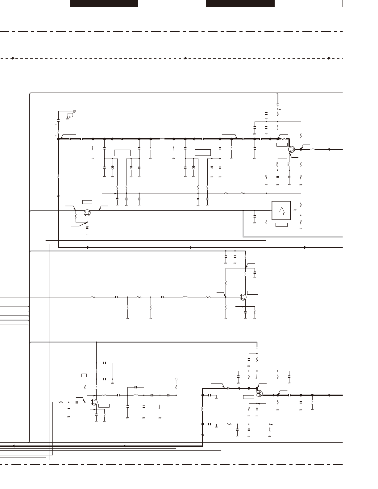
AE AF AG AH AI
NXR-710
C176
1000p
1k
R100
R101
150C_1
50R
C101
C160
1000p
1000p
0
DC SW
14.50V 13.82V
VT2 -->
VT1 -->
14.44V
2SC5383-T111
10k
R107
Q100
C110
SCHEMATIC DIAGRAM
BPF
L100
2.2u35
C105
10p(B)
C102
C103
FL:3.19V
FC:4.44V
FH:7.21V
1000p
10p(B)
FREQUENCY
CONTROL
D100
1SV283F
R105
C104
D100,101
100k
1000p
R106
C106
D101
100k
1000p
C107
C108
1SV283F
C109
7T
1000p
10p(B)
1000p
L101
L102
270n
7T
L103
7T
C112
1000p
FREQUENCY
CONTROL
D103
C113
12p(G)
C115
10p(B)
D103,104
1SV283F
R109
C114
100k
1000p
R110
C116
D104
100k
1000p
C117
C118
1SV283F
-108.0dBm-110.8dBm
1000p
22p(G)
R111
100
C227
TX-RX UNIT (X57-7940-10)
80R
L106
7.90V
22
C122
R117
1000p
68n
L107
C123
0.1u
C120
1000p
C124
C161
R112
100k
R235
22
4.93V
C121
C119
27p
7p(B)
0.1u
VT2
1000p
7T
L104
0.1u
C231
1000p
R115
R113
L105
120
C125
LMC7101BIM5
1
OUTPUT
2
V+
3
INPUT+4INPUT-
10k
7.31V
R137
RF AMP
Q101
2SC5337
27n
1000p
IC100
OP AMP
0
V-
L108
C127
27n
5
2.85V
1000p
R121
R122
R118
R119
3.61V
820
220
270k
39k
L109
22n
VT1 -->
136-174MHz -->136-174MHz -->
LNA
1k
R120
FIN
/RXPCS_TR
SPSD0
C236
56n
1000p
L207
4.7k
22
C347
C832
5p
1.32V
-94.7dBm
R233
1.8k
R234
IF AGC AMP
C300
27p
R302
47k
1.24V
C350
C337
C235
0.01u
Q300
3SK294-FP
RF AMP
0.1u
RF AMP
Q203
2SC5636
1000p
C301
R300
R301
C303
R237
1000p
330
100
0.01u
L300
R303
L301
C302
68
22
R304
3.44V
100k
R305
R306
12k
2.24V
10k
C304
0.01u
C305
0.01u
C306
2p(B)
L302
560n
330n
4.90V
0.82V
0.01u
1’st Lo AMP
R230
C226
R231
18
270
BPF
C228
100p
L205
47n
68p
R227
L203
C221
C222
0.01u
22
C223
0.01u
560n
R229
Q202
2SC5636
RF AMP
R228
0.01u
C224
1000p
C225
0
12p(G)
0
R249
18
33C
50C
LDR
50R
X3
R225
330k
5.04V
0.72V
C220
R223
180
0.01u
0V
10p
C219
C230
C229
1000p
270
R232
C233
47p
68p
L206
100n
C234
47p
CN205
R236
<-- 57.6MHz
L211
15n
1k
R224
<-- 58.05MHz
15p(G)
1u
L317
19.2MHz -->
VT2 -->
VT1 -->
94
X57-794 7/8
Page 95

TX-RX UNIT (X57-7940-10)
3dBm
C667
C680
3p(B)
1000p
8TC
80C
C671
ANAMALAKAJ
SCHEMATIC DIAGRAM
AMP
L610
C672
82n
Q606
2SC5636
RF AMP
1000p
C674
C673
22p
R670
1000p
270
R671
L617
R689
C684
270
1000p
R672
C685
R690
1000p
270
C686
18
1000p
R686
4.7k
SSM3K15TE(F)
HVC131
DC SW
Q607
4.7k
R668
L609
15n
10p
R669
7.82V
2.12V
1.42V
1.8k
22
RF SW
D601
R687
R:7.96V
T:4.26V
4.7k
C687
C679
1000p
1000p
R680
820
1dB ATT
R681
5.6
NXR-710
136-174MHz -->
820
R682
GND SPRING
CN102
C683
1000p
CN106
CN610
0dBm
FINAL UNIT
(X45-3920-10)
(A/3)-CN1
1
2
VT1 -->
136-174MHz -->
C129
C130
1000p
8p
C131
30R
C140
C141
C243
1000p
8p(B)
27p
L210
C142
33n
L112
BPF
L113
270n
7T
1000p
3.00V
L114
C245
7T
15p
R320
L116
C149
C150
1000p
10p(B)
L115
C151
1000p
7T
C152
9T
22p(G)
C322
1000p
C147
10p(B)
D107,108
C144
FREQUENCY
1000p
CONTROL
D107
C145
10p(B)
270
R243
22
C323
4.7u25
1SV283F
R135
C146
3dB ATT
R244
18
C325
100k
1000p
R136
C148
0.1u
D108
1SV283F
100k
1000p
194.05-232.05MHz -->
270
R245
C339
1000p
L117
9T
C156
C154
33p(G)
<-- 136-174MHz
3.3dBm
L308
2.2n
MIXER
IC300
ADL5350ACPZ
L309
100n
L118
9T
C158
33p(G)
136-174MHz -->
C331
1000p
4
NC1
GND16VPOS7NC28RF/IF
5
2.76V
10T
L119
110n
22p(G)
39n
L312
27p
C332
1
2
3
LoIN
GND2
RF/IF1
27p
L315
C333
R128
R125
0
1
2
3
0.1u
10k
R126
0
IC101
LMC7101BIM5
OUTPUT
V+
INPUT+4INPUT-
OP AMP
C237
8p(B)
R129
5
V-
-122.0dBm
C134
0
1000p
7T
L111
R132
100k
FL:2.72V
FC:4.22V
FH:6.74V
R130
270k
39k
R131
R238
0
18p
C239
L208
C138
10p(B)
D105,106
C135
FREQUENCY
1000p
CONTROL
C136
D105
8p(B)
R114
100
33n
1SV283F
R133
C137
C241
27p
100k
1000p
R134
C139
L209
D106
1SV283F
100k
1000p
LPF
33n
39n
CN101
-118.0dBm
RX ANT
3
4
5
80R
MCF
-113.6dBm -101.4dBm
C356
10p
C318
27p(G)
R323
150
XF300
L71-0649-05
C326
33p(G)
L310
330n
INOUT
C329
0.01u
R316
C342
10
18p
C344
C343
0.01u
0.01u
C345
R314
1000p
10k
Note : The components marked with a dot (•) are parts of layer 1.
R856
L303
22
330n
7.21V
R311
10
RF AMP
Q301
2SC5337
R315
C334
0.01u
R332
47
<-- 58.05MHz
22
R318
C349
0.01u
2.7k
R313
IF POST AMP
2.26V
-115.7dBm
C338
R312
10
1.53V
L804
100
C341
R310
120n
0.01u
L320
0.01u
180n
18p
1.2k
C346
L313
C335
27p
82n
L316
270n
C336
82p
6
7
95
X57-794 8/8
Page 96
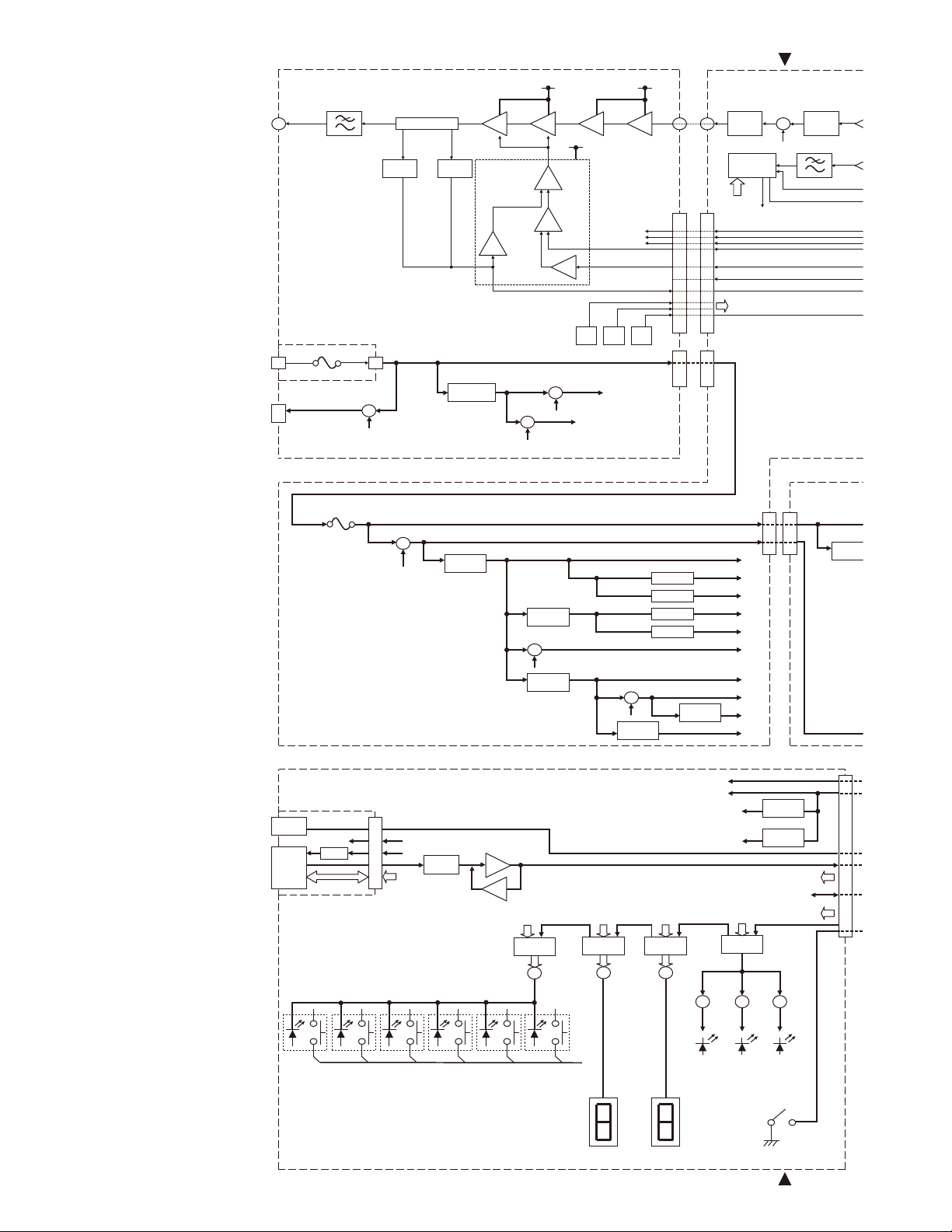
NXR-710
T
2
F
2
4
BLOCK DIAGRAM
FINAL UNIT (X45-392)
TX ANTENNA
Power Supply
+B
CN205
FAB
LOW PASS FILTER
TX-RX UNIT (X57-794)
D601
1dB
ATT
MOD PLL IC
IC602
ADF4001BRUZ
SPSCLK0
SPSD0
/16_8PCS
TMP1
TMP2
HVC131
SW
8TC
LDT
CN610
CN801
CN701
FAN
ASWC
RAMP
H/L
FDT
HWV2
3dB
ATT
LOW PASS FILTER
BUF
Q606
2SC5
AMP
Q60
2SC
FINAL AMP
Q4
FW DETREV DET
RD70HVF1-101
FW DET
AVR
IC203
NJM78M08FA-ZB
CM COUPLER
REV DET
CN201
SW
FAN
DRIVE AMP
Q3
PD55003S-E
Vcont
DC AMP
IC202(A/2)
TA75W01FUF
BUFFER AMP
IC202(B/2)
TA75W01FUF
+B
REF AMP
IC201(A/2)
TA75W01FUF
SW
8TC
DRIVE AMP
Q2
2SC3357-A
Auto Power
Control
LIMITER AMP
IC201(B/2)
TA75W01FUF
Temp1 Temp2
SW
ASWC
80T
ANT8V
80T
DRIVE AMP
Q1
2SC3357-A
80T
CN1
CN204
8TC 8TC
FAN
ASWC
PLIM PLIM
RAMP
H/L
FDT
TMP1
TMP2
HWV2
CN203
Hard Ware
Version
CONTROL UNI
CN700
CN301
DISPLAY UNIT (X54-358)
Volume
VR601
MIC JACK
J601
VLI
D603
PTT/TXD
HK/RXD
5M
SB
MIC
SB
SW
5M
SB
PTT/TXD
HK/RXD
CN601, CN501
AVR
IC704
TK11230CMCL
33C
Q521~524
UPA627T-A
SW SW SW
SB
80C_1
80C_2
150C_1
150C_2
Q508,Q504
30R
50M
SB
5V
5V
CLK, SOE,
STB1, DAT
Shift Reg.4
IC502
BU4094BCFV
Q503,Q504,
Q506,Q509
AVR
IC506
TA78L05FF
AVR
IC507
TA78L05FF
PTT/TXD
HK/RXD
KEY1~5
DAT,CLK,SOE,STB1
Q507,Q510,
Q511
DC-DC
IC301
LT3685EM
CN50
VLI
MIC
PSW
80C
AVR
VR501
IC702
NJM78M08FA
AGC AMP
AMP
IC501
NJM4558E-ZB
CLK, SOE,
STB1, DAT
Shift Reg.1
BU4094BCFV
DC-DC
IC701
XC9101D09AKR
80R
SW
RXC
AVR
IC700
NJM78M05DL
IC503
SW
Q512~514
UPA627T-A
150C
50C
CLK, SOE,
STB1, DAT
Shift Reg.2
IC504
BU4094BCFV
SW
Q516~519
UPA627T-A
SW
RXC
AVR
IC703
TK71733S
50R
BU4094BCFV
Ripple Filter
Ripple Filter
Ripple Filter
Ripple Filter
CLK, SOE,
STB1, DAT
Shift Reg.3
IC505
SW
SBC
96
S501 S502 S503 S504 S505 S506
KEY1~5
D506
7SEGMENT
D507
7SEGMENT
D504
D503
LED
LED
Q503,504,507: UPA672T-A
Q506,508~511: RT1P141M-T111
D505
LED
S507
Page 97
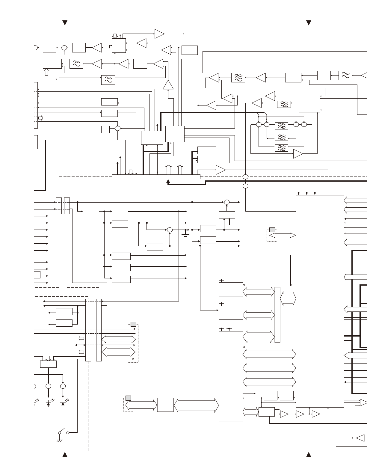
BLOCK DIAGRAM
X
X
(
2
P
NXR-710
TX-RX UNIT (X57-794)
D601
1dB
ATT
MOD PLL IC
IC602
ADF4001BRUZ
SPSCLK0
SPSD0
/16_8PCS
TMP1
TMP2
50M
SB
5V
5V
CLK, SOE,
STB1, DAT
Shift Reg.4
IC502
LDT
CN700
HVC131
SW
8TC
AVR
IC506
TA78L05FF
AVR
IC507
TA78L05FF
DAT,CLK,SOE,STB1
CN610
CN801
CN701
SB
80C_1
80C_2
150C_1
150C_2
MCL
8TC
FAN
ASWC
PLIM
RAMP
H/L
FDT
HWV2
30R
BU4094BCFV
SPSCLK0,SPSD0
TXVCOA,TXVCOB,
/TXPCS
BUFFER
Q606
2SC5636
3dB
ATT
LOW PASS FILTER
AMP
Q602
2SC4617(R)
LOOP FILTER
LEVEL CONV
TC75S51FE(F)
LEVEL CONV
TC75W51FK(F)
Hard Ware
Version
CONTROL UNIT (X53-449)
CN301
DC-DC
IC301
LT3685EMSE
CN502
CN40
KEY1~5
PTT/TXD
HK/RXD
VLI
MIC
PSW
VLI_DIS
MIC
/PSW
LDT
TX
VCO/PLL
X58-5080-10
16.8MHz
BUFFER
Q603
2SC4617(R)
IC801
IC803
IC806
TC7W53FK(F)
SW
SBC
33A
CN800
60DC
AVR
IC302
XC6201P502PR
AVR
IC303
XC6204B332P1
AVR
IC305
XC6205B162PR
AVR
IC304
XC6205B152PRN
AVR
IC306
XC6204B332P1
RXD2_DIS
TXD2_DIS
KEYI[0~2], KEYO[0~1]
SPSCLK1_DIS
SPSD1_DIS
SR_OE_DIS
ASSIST AMP
IC607
LMC7101BIM5
16.8MHz
LDT
LDR
RSSI
TMP1
TMP2
50M
33M
16M
15M
33A
C
CV AMP
IC608
TC75W51FK(F)
OSC
X600
MCP23S08TE/ML
SPSCLK1,SPSD1
TXASSIST
AMP
IC604
LMC7101BIM5
AMP
IC603
TC75S51FE(F)
I/O Expander
IC805
MOD
LD
IO CS
RESET
IC308
XC6109C29ANN
MOD AMP
IC606
LMC7101BIM5
RXC
/EWP
Q303
2SA1955A-F
SPSCLK0
SPSD0
/16_8PCS
/RST
MO
MB
EVOL
IC804
M62364FP-F
33BU
SW
TX_CV
TXASSIST
RXASSIST
TX_CV
RX_CV
TXCOB
RXVCOA/B
TXVCOA
/RXPCS_TR
/TXPCS
VREF
IC605
TC75S51FE(F)
I2CCK, I2CDA
IF AGC AMP
Q300
2SK294-FP
AMP
IC409(A/2, B/2)
TC75W51FK(F)
RSSI
RSSIOFS
TEMP
IC800
LM73CIMKX-0
E2PROM
IC802
M24C02-RMN6TP
AGC
/OVRB
Q301
RT1N441U-T111
/BINT
IC307
XC61CN2702N
/RST
BUFFER
IC402
LMC7101BIM5
Q401
RT1N141M-T111
/OVRB
/BINT
33M
E29PL03270TIP
33BU
33M 16M
SW
OR
FLASH
SRAM
Diff AMP
IC401(B/2)
TC75W51FK(F)
AMP_B
Q402
2SJ506-E(S)
AMP_SW
IC3
IC9
DSP
IC6
MCF
IF AMP
Q301
2SC5337
58.05MHz
BUFFER
IC401(A/2)
TC75W51FK(F)
450kHz
IF AMP
IC400
AD8051ART
IC405~408: TC7W53FK(F)
SW
CN802
CN39
/FRST
A[0~21], D[0~15]
/RD, /WR, /CS0, /WP
A[0~17], D[0~7]
/RD, /WR, /CS2
A[0~20], D[0~15],
/RD, /WR, /HRDY, /CS3,
/HDS2
/DRST
MCDICN, MCDOCN, MCSCKCN
CF (Narrow)
SW
IC405 IC406 IC408 IC407
CF (VNarrow)
A
/MCCSXCN, /MCCSRCN,
MCSCKAF, /MCCSAF,
MCDIAF, MCDOAF
CF (Wide)
AO[1~5]
ADL5350ACPZ
CF
IC300
IFR
1st Lo AM
194.05~
232.05MHz
IF-IC
IC403
NJM2287V
SW
IF AMP
IC404
MCP6021-E/0T
3dB ATT
LOW PASS FILTER
AGC
33A15M33M
MCU
IC20
I2CCK, I2CDA
SPSCLK1, SPSD1
MIX
RSSI
IF
SW
/FRST
/DRST
Q203
2SC5636
/485_RE1, RXD1, T
/485_RE2, RXD3, T
KEYI[0~2], KEYO[0~1
/PSW
VLI
MICADC0
PTT, TXD0, TXD2
/IOINT, EPTT, HK
RXD0, RXD2
/RINT, 32K
SW SW
Q508,Q504
Q503,Q504,
Q506,Q509
D504
3
LED
503,504,507: UPA672T-A
506,508~511: RT1P141M-T111
D505
LED
S507
Q507,Q510,
Q511
CN44
DSUB 25PIN
B
BER_CLK_5V
BER_DATA_5V
LEVEL
CONVERTOR
(3.3V→5V)
IC23
TC7WT125FUF
/BER_EN
/BER_CLK
/BER_DATA
/SYMTIM, /DINT, /DWUP, FSDET, /HINT
/PCS_DSP
MAIN_CLK
/PDN, LRCLK,
SDTI, BICLK
BUFFER
IC16
SM5023CNDH-G
Squelch DAC
IC14
AK4386VTP
VREF
VCTCXO
X1
(18.432MHz)
AMP
IC13(A/2,B/2)
TC75W51FK(F)
BSHIFT
XTAL_IN
LDR
AMP
Q4
2SC4617(S)
ADC1
AMP
IC15(A/2)
TC75W51FK(F)
MICADC1
SPDAC
PWM1
97
VREF
VREF
AMP
IC411
NJM
REF AMP
IC405(B/4)
NJM2734V
Page 98

NXR-710
BLOCK DIAGRAM
IF AMP
Q301
2SC5337
58.05MHz
ADL5350ACPZ
BUFFER
IC401(A/2)
TC75W51FK(F)
IC405~408: TC7W53FK(F)
CF (Narrow)
SW
CF (VNarrow)
CF (Wide)
A
BUFFER
IC16
VREF
CF
AO[1~5]
VCTCXO
(18.432MHz)
AMP
IC13(A/2,B/2)
TC75W51FK(F)
X1
z
IF AMP
IC400
AD8051ART
SW
IC405 IC406 IC408 IC407
802
39
T
A[0~21], D[0~15]
RD, /WR, /CS0, /WP
A[0~17], D[0~7]
/RD, /WR, /CS2
A[0~20], D[0~15],
/HDS2
T
/MCCSXCN, /MCCSRCN,
MCDICN, MCDOCN, MCSCKCN
MCSCKAF, /MCCSAF,
MCDIAF, MCDOAF
/SYMTIM, /DINT, /DWUP, FSDET, /HINT
SP
_CLK
SM5023CNDH-G
Squelch DAC
LRCLK,
IC14
BICLK
AK4386VTP
MIX
IC300
IFR
SW
/FRST
/DRST
BSHIFT
XTAL_IN
194.05~
232.05MHz
RSSI
IF
NJM2287V
SW
IF AMP
IC404
MCP6021-E/0T
LDR
AMP
Q4
2SC4617(S)
IF-IC
IC403
33A15M33M
AMP
IC15(A/2)
TC75W51FK(F)
3dB ATT
MCU
IC20
AGC
I2CCK, I2CDA
SPSCLK1, SPSD1
ADC1
LOW PASS FILTER
MICADC1
SPDAC
PWM1
KEYI[0~2], KEYO[0~1]
/PSW
VLI
MICADC0
10MHz or 19.2MHz
SPSCLK0,SPSD0
RXVCOA/B,
/RXPCS_TR
1st Lo AMP
Q203
2SC5636
/485_RE1, RXD1, TXD1, 485_DE1
/485_RE2, RXD3, TXD3, 485_DE2
PTT, TXD0, TXD2
/IOINT, EPTT, HK
RXD0, RXD2
/RINT, 32K
VREF
VREF
LEVEL CONVERTOR
TC74VHCT244AFK
LEVEL CONVERTOR
TC7MBD3245AFK
R2023T
TMP, HWV1, HWV2, FWD, TXASSIST, RXASSIST, TX_CV, RX_CV, AGC, TXVCOB, TXCOA, RXCOA/B, LDT, LDR
RAMP_TX
AMP
IC411(A/4)
NJM2734V
REF AMP
IC405(B/4)
NJM2734V
SW
D504,505
JDP4P02AT
LDR
RX
VCO/PLL
X58-5070-10
57.6MHz
136~174MHz
LEVEL CONVERTOR
IC7:TC7WT125FUF
IC10:TC7SH125FU-F
LEVEL CONVERTOR
IC8:TC7WT125FUF
IC11:TC7SH125FU-F
AMP
IC405(C/4)
NJM2734V
(3.3V→5V)
IC18
TXD0_RS
/FRST_IO
RXD2_DIS
RXD0_RS
(3.3V↔5V)
IC19
IOINT_5V
I2C_5V
EPTT_5V
/RST
RTC
IC17
X
X2
32.768kHz
VREF
/16_8PCS, /TXPCS, SPSCLK0, SPSD0, /EWP, /IOCS, /EVCS, SBC
AMP
IC28
TC75S51FE(F)
VREF
AMP
IC411(D/4)
NJM2734V
AMP
IC411(C/4)
NJM2734V
/EVDSCS_EV,
SPSCLK1,
SPSD1
1dB ATT
REF
1dB ATT
AMP
IC201
LMC7101BIM5
BAND PASS FILTER
SR_STR
STR_SEL
/EVDSCS
STR_SEL
AMP
IC406(A/2,B/2)
NJM2732V
MODDAC
VREF
DAC
IC412
M62364FP-F
/AF_MUTE
LOW PASS FILTER
RXASSIST
_
RAMP
TA
AMP
Q504
2SC4617(R)
CV AMP
IC200
TC75W51FK(F)
LOW PASS FILTER
LNA AMP
Q101
2SC5337
BUFFER AMP
IC100
LMC7101BIM5
AMP
IC27(A/2,B/2)
TC75W51FK(F)
SPSCLK1_DIS, SPSD1_DIS
SELECTOR
AND GATE
IC26
TC7SET08FU-F
SELECTOR
OR GATE
IC25
TC7SH32FU-F
AMP
IC404(A/2)
NJM2732V
AMP
IC405(A/4)
NJM2734V
TD
SW
TD_SW
AMP
IC411(B/4)
NJM2734V
SW
IC402
TC7S66FUF
DETECTOR
D503
HSM88AS-E
TXD2_DIS
RD
IC407
TC7W53FK(F)
RA
Q405
DTC363EU
LOW PASS FILTER
x3
Q202
2SC5636
BAND PASS FILTER
TRANSCEIVER
ISL8485EIBZ
TRANSCEIVER
ISL8485EIBZ
SR_STR_DIS
/EVDSCS_EV
TA
AMP
IC405(D/4)
NJM2734V
TD
TD
NAND GATE
TC7SH00FU-F
SW
AMP
IC500 (B/2)
TC75W51FK(F)
RX_CV
IC4
IC5
BUFFER
ADM101EARMZ
I/O Expander
MCP23017TE/ML
SELECTOR
IC401
IC21
IC22
BUFFER AMP
IC101
LMC7101BIM5
AMP
IC500 (A/2)
TC75W51FK(F)
AGC AMP
Q503
3SK294-FP
AMP
Q502
2SK3737-5
LOW PASS FILTER
N_SYNC1_A, N_SYNC1_B
N_SYNC2_A, N_SYNC2_B
to CN40 DISPLAY
VLI_DIS
MIC
SR_OE_DIS
TXD0_RS, RXD0_RS
SC, EXT_MON
AUXIO[1~6]
AI[1~3]
B
to
LEVEL CONVERTOR
IC23
/PCS_DSP
/RXPCS
AMP
IC404(B/2)
VREF
NJM2732V
AMP
IC15(B/2)
TC75W51FK(F)
to MCU
IC20
A
AO[1~5]
AMP_B
Power
AMP
LA4422-E
/PSW
BUFFER
Q501
2SC4617(R)
19.2MHz
N_SYNC
BER_CLK_5V
BER_DATA_5V
33A
RXPCS_TR
SELECTOR
AND GATE
IC24
TC7SH08FU-F
MOD
RSSI
SB
EXT_RSSI
Q6~10
SPO
SPO
OSC
X500
RX ANTENNA
136~174MHz
CN5
C
CN44
DSUB25
RD
TA
TD
RA
SPM
CN38
CN41
CN42
SPI
CN43
EXT_IN
10MHz
TX-RX
TEST/SPKR
98
Page 99
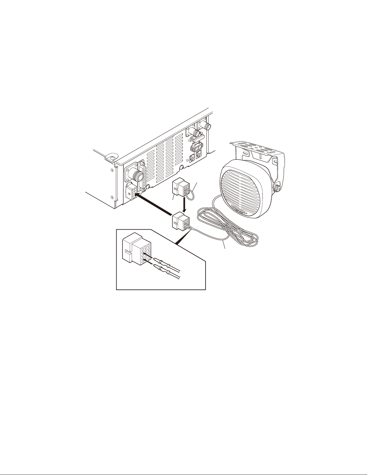
NXR-710
OPTIONAL ACCESSORIES: KES-5 (EXTERNAL SPEAKER)
When Using an External Speaker
1. Make sure the unit’s power is tuned off.
2. When using the external speaker, remove the jumper
lead from the connector, and attach the speaker cable.
3. When not using the external speaker, replace the jumper
lead and insert the connector into the speaker jack (pin 9
and 12).
Connector
Specifi cations
Maximum input power ................................................... 40W
Impedance ......................................................................... 4
Dimensions (W x H x D) projection not included
.................129 x 129 x 77 mm (5-1/16 x 5-1/16 x 3 inches)
Weight ............................................................ 820g / 1.81 lbs
Jumper lead
KES-5
Ω
13
15
12
1
6
3
Crimp terminal
(E23-0613-05)
Speaker cable
Black lead
Black/White lead
99
Page 100

NXR-710
SPECIFICATIONS
General
Frequency Ranges ............................................ 136~174MHz
Number of Channels ...........................................................30
Channel Spacing
Analog ..................................................12.5/ 15/ 25/ 30kHz
Digital ...............................................6.25/ 7.5/ 12.5/ 15kHz
PLL Channel Step .............................................2.5/ 3.125kHz
Antenna Impedance ........................................................50
Operating Voltage .......................................... 10.8~15.6V DC
Current Drain
Standby ....................................................................... 0.5A
Receive ....................................................................... 1.0A
Transmit .................................................................... 11.0A
TX Power
50% Duty .................................................................... 50W
100% Duty .................................................................. 25W
Operating Temperature Range
......................................... –22°F~+140°F (–30°C~+60°C)
Frequency Stability .................................................. ±1.0ppm
Dimension (W x H x D) (Projections not included)
.........19.00 x 3.46 x 13.39 inches (482.6 x 88 x 340 mm)
Weight (net) ................................................... 21.4 lbs (9.7kg)
Receiver
Sensitivity
Digital@6.25kHz (3% BER) ......................................0.22µV
Digital@12.5kHz (3% BER) ......................................0.28µV
Analog (12dB SINAD) ...............................................0.28µV
Sensitivity
Analog@25kHz ........................................................... 83dB
Ω
Analog@12.5kHz ........................................................ 77dB
FM Hum & Noise
Analog@25kHz ........................................................... 55dB
Analog@12.5kHz ........................................................ 50dB
Intermodulation Distortion ............................................. 80dB
Spurious Response ........................................................ 90dB
Audio Distortion (Ext. SP) ............ Less than 2.5% at 1000Hz
Audio Output (Ext. SP) ....4W (at 4Ω, less than 5% distortion)
Transmitter
RF Power Output ......................................................25~50W
Spurious & Harmonics ................................................... 80dB
FM Hum & Noise
Analog@25kHz ........................................................... 55dB
Analog@12.5kHz ........................................................ 50dB
Audio Distortion .............................. Less than 1% at 1000Hz
Modulation .............16K0F3E, 11K0F3E, 8K30F1E, 8K30F1D,
8K30F7W, 4K00F1E, 4K00F1D,4K00F7W, 4K00F2D
Analog measurements made per TIA/EIA 603 and specifi cations shown are typical.
KENWOOD reserves the right to change specifi cations without prior notice or obligation.
2967-3, Ishikawa-machi, Hachioji-shi, Tokyo, 192-8525 Japan
P.O. BOX 22745, 2201 East Dominguez Street, Long Beach,
CA 90801-5745, U.S.A.
6070 Kestrel Road, Mississauga, Ontario, Canada L5T 1S8
Rembrücker Str. 15, 63150 Heusenstamm, Germany
Leuvensesteenweg 248 J, 1800 Vilvoorde, Belgium
L’Etoile Paris Nord 2, 50 Allée des Impressionnistes,
Bp 58416 Villepinte, 95944 Roissy Ch De Gaulle Cedex
KENWOOD House, Dwight Road, Watford, Herts.,
WD18 9EB United Kingdom
Amsterdamseweg 37, 1422 AC Uithoorn, The Netherlands
Via G. Sirtori, 7/9 20129 Milano, Italy
Bolivia, 239-08020 Barcelona, Spain
Talavera Business Park Building A, 4 Talavera Road,
North Ryde NSW 2113 Australia
Unit 3712-3724, Level 37, Tower one Metroplaza, 223 Hing Fong Road,
Kwai Fong, N.T., Hong Kong
1 Ang Mo Kio Street 63, Singapore 569110
 Loading...