

Kenwood NX-820, NX-820 C Service Manual
UHF DIGITAL TRANSCEIVER / UHF 数字模拟双模车载对讲机
NX-820
SERVICE MANUAL /
维修手册
C version / C 版本
Modular jack
(E58-0535-05)
模块化插孔
/
Key top
(K29-9479-01)
/
按键
Panel assy
(A62-1200-03)
/
© 2012-11 PRINTED IN CHINA
B53-7046-00 (Y)
面板组件
徽标
/
Badge
(B43-1675-04)
http://www.kenwoodhk.com.hk/
This product complies with the
directive for the European market.
RoHS
This product uses Lead Free solder.

NX-820
CONTENTS /
GENERAL ....................................................3
SYSTEM SET-UP .........................................5
REALIGNMENT ...........................................6
INSTALLATION ..........................................11
DISASSEMBLY FOR REPAIR ...................15
CIRCUIT DESCRIPTION ...........................19
COMPONENTS DESCRIPTION ................28
PARTS LIST ...............................................32
EXPLODED VIEW ......................................43
TROUBLE SHOOTING ..............................44
ADJUSTMENT ...........................................50
TERMINAL FUNCTION .............................90
PC BOARD
DISPLAY UNIT (X54-3830-10) ...............98
目录
概 述 ............................. 3
系统体系 ............................. 5
模式组合 ............................. 6
安 装 ............................ 11
维修拆卸 ............................ 15
电路说明 ............................ 19
元件说明 ............................ 28
零 件 表 ............................ 32
部件分解图 .......................... 43
故障排除 ............................ 45
调 整 ............................ 51
端子功能 ............................ 90
印刷电路板
显示单元 (X54-3830-10) ............ 98
TX-RX UNIT (X57-8240-13) ..................100
INTERCONNECTION DIAGRAM .............104
SCHEMATIC DIAGRAM ..........................105
BLOCK DIAGRAM ...................................116
LEVEL DIAGRAM ....................................119
SPECIFICATIONS ....................................120
Document Copyrights
Copyright 2012 by JVC KENWOOD Cor poration. All
rights reserved.
No part of this manual may be reproduced, translated,
distributed, or transmitted in any form or by any means,
electronic, mechanical, photocopying, recording, or otherwise, for any purpose without the prior written permission of
JVC KENWOOD Corporation.
收发单元 (X57-8240-13) ........... 100
互 连 图 ........................... 104
原 理 图 ........................... 105
方 块 图 ........................... 116
电 平 图 ........................... 119
规 格 .......................... 121
文档版权信息
JVC 建伍株式会社拥有版权 2012。保留所有权利。
未经 JVC 建伍株式会社预先书面同意,无论出于何种目的,
均不得以任何形式或任何方式包括电子、机械、影印、录音
或其他方式复制、翻译、分发或传播本手册的任何部分。
Disclaimer
While every precaution has been taken in the preparation
of this manual, JVC KENWOOD Corporation assumes no
responsibility for errors or omissions. Neither is any liability
assumed for damages resulting from the use of the information contained herein. JVC KENWOOD Corporation reserves
the right to make changes to any products herein at any time
for improvement purposes.
2
免责声明
JVC 建伍株式会社在准备本文档时已采取所有必要的预防
措施,恕不对错误或疏漏承担任何责任,也不对因使用本文
中所含的信息而导致的损害负责。JVC 建伍株式会社保留出于
改进的需要而随时对文中的产品信息做出更改的权利。

NX-820
GENERAL /
INTRODUCTION
SCOPE OF THIS MANUAL
This manual is intended for use by experienced technicians familiar with similar types of commercial grade com mu ni ca tions equipment. It contains all required service
in for ma tion for the equipment and is current as of the publication date. Changes which may occur after publication
are covered by either Service Bulletins or Manual Revisions.
These are is sued as required.
ORDERING REPLACEMENT PARTS
When ordering replacement parts or equipment information, the full part identifi cation number should be included.
This applies to all parts : components, kits, or chassis. If the
part number is not known, include the chassis or kit number
of which it is a part, and a suffi cient description of the re quired component for proper identifi cation.
PERSONAL SAFETY
The following precautions are recommended for personal
safety:
• DO NOT transmit if someone is within two feet (0.6 me-
ter) of the antenna.
• DO NOT transmit until all RF connectors are secure and
any open connectors are properly terminated.
• SHUT OFF this equipment when near electrical blasting
caps or while in an explosive atmosphere.
• All equipment should be properly grounded before pow-
erup for safe operation.
• This equipment should be serviced by only qualifi ed tech-
nicians.
概述
引言
本手册的范围
本手册是提供给熟悉通信专业并且具有维修经验的技术人
员使用的。它包括了维修该设备所需要的全部资料和现行出
版日期。在出版后可能发生变动,如果需要,可以参照《维
修通报》或《手册修订本》进行补充。
替换零件的订购
当订购替换零件或设备资料时,应注意完整的零件识别号
码。所有的零件均有识别号码∶元件,组件或机壳。如果不
知道零件的号码,为了正确地识别,必须注明此元件所属的
机壳或组件的号码,并对元件进行充分的说明。
个人安全
为了个人的安全,请注意下列事项∶
• 如果有人在天线两英尺 (0.6 米 ) 范围之内时,不要进行
发射。
• 在没有认真核实所有射频插头之前或有任何一个脱开的插
头没有连接到相应端口上的情况下均不要发射。
• 在电爆管附近或在易燃性气体环境中,必须关闭电源,不
要操作本设备。
•
为了操作的安全,在接通电源之前所有设备应该连接地线。
• 本设备只应该由有资格的技术人员进行维修。
PRE-INSTALLATION CONSIDERATIONS
1. UNPACKING
Unpack the radio from its shipping container and check
for accessory items. If any item is missing, please contact
KENWOOD immediately.
2. PRE-INSTALLATION CHECKOUT
2-1. Introduction
Each radio is adjusted and tested before shipment. However, it is recommended that receiver and transmitter operation be checked for proper operation before installation.
2-2. T esting
The radio should be tested complete with all cabling and
accessories as they will be connected in the fi nal installation.
Transmitter frequency, deviation, and power output should be
checked, as should receiver sensitivity, squelch operation,
and audio output. Signalling equipment operation should be
verifi ed.
安装前条件
1. 开箱
从运输包装中取出本无线电设备并检查附件。如果有任何
组件遗失,请立即与 KENWOOD 联系。
2. 安装前检查
2-1. 说明
在运输之前每一台无线电设备均已调整和测试过。但是,
在安装之前最好检查接收和发射以便操作正确。
2-2. 测试
无线电设备应该按照电缆和附件最终安装时的连接进行完
整的测试。应该检查发射频率,频偏和输出功率,同样应该
检查接收灵敏度,静噪和音频输出。应该检验信令操作。
3

NX-820
GENERAL /
3. PLANNING THE INSTALLATION
3-1. General
Inspect the vehicle and determine how and where the ra-
dio antenna and accessories will be mounted.
Plan cable runs for protection against pinching or crush-
ing wiring, and radio installation to prevent overheating.
3-2. Antenna
The favored location for an antenna is in the center of a
large, flat conductive area, usually at the roof center. The
trunk lid is preferred, bond the trunk lid and vehicle chassis
using ground straps to ensure the lid is at chassis ground.
3-3. Radio
The universal mount bracket allows the radio to be
mounted in a variety of ways. Be sure the mounting surface
is adequate to support the radio’s weight. Allow sufficient
space around the radio for air cooling. Position the radio
close enough to the vehicle operator to permit easy access
to the controls when driving.
3-4. DC Power and wiring
1. This radio may be installed in negative ground electrical
systems only. Reverse polarity will cause the cable fuse
to blow. Check the vehicle ground polarity before installa-
tion to prevent wasted time and effort.
2. Connect the positive power lead directly to the vehicle
battery positive terminal. Connecting the Positive lead to
any other positive voltage source in the vehicle is not rec-
ommended.
3. Connect the ground lead directly to the battery negative
terminal.
4. The cable provided with the radio is suffi cient to handle
the maximum radio current demand. If the cable must be
extended, be sure the additional wire is suffi cient for the
current to be carried and length of the added lead.
概述
3. 安装的步骤
3-1. 概述
检查车辆并确认如何以及在何处安装无线电天线和附件。
安排好电缆的位置,避免挤压或碾碎布线,同时无线电设
备避免过热。
3-2. 天线
天线的最佳位置应该在一个宽阔,平整导电区域的中心,
通常在车顶的中心。行李箱的盖子更好,将地线黏结在行李
箱的盖子和车辆的外壳上确保行李箱盖子接地。
3-3. 无线电设备
通用安装托架允许以多种方法安装无线电设备。确认安装
的表面足以支撑无线电设备的重量。无线电设备的周围留出
适当的空间进行散热。将无线电设备尽可能的安装在靠近车
辆操作者的位置上,以便在驾驶时易于控制。
3-4. 直流电源和布线
1. 本无线电设备只能被安装在负极接地电子系统中。反向极
性将导致电缆保险丝熔断。在安装之前检查车辆的接地极
性,避免工作效率低以及浪费时间。
2. 将电源的正极引线直接连接到车载电池的正极端点上。不
要将正极引线与车辆上的其他正极电压连接。
3. 将接地引线直接与电池的负极连接。
4. 与无线电设备一起提供的电缆适用于所需的最大无线电电
流。如果电缆必须加长,要确认附加的电线适用于所载的
电流和添加引线的长度。
4. INSTALLATION PLANNING – CONTROL STATIONS
4-1. Antenna system
The antenna system selection depends on many factors and is beyond the scope of this manual. Your KENWOOD dealer can help you select an antenna system that
will best serve your particular needs.
4-2. Radio location
Select a convenient location for your control station radio
which is as close as practical to the antenna cable entry
point. Secondly, use your system’s power supply (which supplies the voltage and current required for your system). Make
sure suffi cient air can fl ow around the radio and power supply to allow adequate cooling.
SERVICE
This radio is designed for easy servicing. Refer to the
schematic diagrams, printed circuit board views, and alignment procedures contained in this manual.
4
4. 安装步骤 - 基站
4-1. 天线系统
天线系统的选择取决于许多因素和本手册的范围。用户的
KENWOOD 销售商可以帮助用户选择最能满足用户特殊要求的天
线系统。
4-2. 无线电位置
为用户的基站无线电设备选择一个方便的位置,此位置应
尽量靠近天线电缆输入点。其次,使用用户系统的电源 ( 为
用户的系统提供所需的电压和电流 )。确认无线电设备周围的
空气流通顺畅并且足以使电源冷却。
维修服务
为了便于维修本设备,建立了完整的维修服务体系,提供
了包括原理图,印刷电路板图和调整步骤在内的资料供参考。
NX-820
GENERAL /
NOTE
If you do not intend to use the speaker 3.5-mm jack and
the D-sub 15-pin connector, fi t the supplied speaker-jack
cap and ACC cap to stop dust and sand from getting in.
Speaker
jack cap
ACC.
Antenna
connector
ACC. cap
Power input
connector
概述
注意
如果不打算使用 3.5mm 扬声器插孔和 15 针 D-sub 连接器,
请装上附带的扬声器插孔盖和 ACC. 盖,防止灰尘和沙粒进入。
外部扬声
Speaker
jack cap
器插孔盖
ACC.
Antenna
天线连接器 ACC. 盖
connector
ACC. cap
Power input
电源输入连接器
connector
SYSTEM SET-UP /
Merchandise received /
Choose the type of transceiver
选择车载对讲机的类型
Transceiver programming /
KES-3
External speaker
外部扬声器
接收到的商品
车载对讲机编程
Connection cable
(Option)
( 可选件 )
系统体系
Frequency range (MHz)
频率范围
400~470 25W
See page 7.
A personal computer, programming interface (KPG-46A/46U),
and FPU (programming software) are required for programming.
参见第7页。
需使用个人电脑、编程接口 (KPG-46A/46U) 和 FPU ( 编程软件 ) 进行编程。
KCT-60
连接电缆
Extension cable /
(Option)
( 可选件 )
KCT-18
Ignition sense cable
点火感应电缆 外部扬声器
See page 12. See page 13.
参见第 12 页。
(Option)
See page 11.
参见第 11 页。
KCT-36
延长电缆
External speaker
( 可选件 )
RF power
射频功率 类型
(Option) *Only when required.
( 可选件 )* 仅在需要的时候。
(Option)
( 可选件 )
KES-5
参见第 13 页。
Type
NX-820 C
Delivery /
交货
5
NX-820
REALIGNMENT /
1. Modes
User mode
Panel test mode
PC mode
Firmware
programming mode
Clone mode
Firmware version information
Mode Function
User mode For normal use.
Panel test mode
Panel tuning mode Used by the dealer to tune the transceiver.
PC mode
Data programming
mode
PC test mode
PC tuning mode Used to tune the transceiver using the PC.
Firmware programming mode
Clone mode
Firmware version
information
Use by the dealer to check the fundamental
characteristics.
Used for communication between the transceiver and PC.
Used to read and write frequency data and
other features to and from the transceiver.
Used to check the transceiver using the PC.
This feature is included in the FPU.
Used when changing the main program of
the fl ash memory.
Used to transfer programming data from one
transceiver to another.
Used to confi rm the internal fi rmware version.
Panel tuning mode
Data programming mode
PC test mode
PC tuning mode
模式组合
1. 模式
⭞ᡭ⁗ᕅ
䶘ᶵ⎁䈋⁗ᕅ
3& ⁗ᕅ
രԬ㕌ぁ⁗ᕅ
གྷ⁗ᕅ
രԬ⡾ᵢؗᚥ
模 式 功 能
用户模式 一般使用。
面板测试模式 用于经销商检查基本功能。
面板调谐模式 用于经销商调整车载对讲机指标。
PC 模式 用于车载对讲机与 PC 之间的通信。
数据编程模式 用于阅读和写入频率数据以及其他功能。
PC 测试模式
PC 调谐模式 用于通过 PC 调谐车载对讲机。
固件编程模式 当改变闪存中操作主程序时使用。
复制模式
固件版本信息 用于确认内部固件版本。
用于通过 PC 检查车载对讲机。
该功能内置于 FPU 中。
用于将一台车载对讲机的编程数据传送到另
一台。
䶘ᶵ䈹䉆⁗ᕅ
ᮦᦤ㕌ぁ⁗ᕅ
3& ⎁䈋⁗ᕅ 3& 䈹䉆⁗ᕅ
2. How to Enter Each Mode
Mode Operation
User mode Power ON
Panel test mode [
Panel tuning mode Panel test mode + [
PC mode Received commands from PC
Firmware programming mode [
Clone mode [
Firmware version information [
] + Power ON
] + Power ON
] + Power ON (One second)
] + Power ON
3. Panel Test Mode
Setting method refer to ADJUSTMENT.
4. Panel Tuning Mode
Setting method refer to ADJUSTMENT.
6
2. 如何进入每一种模式
模 式
用户模式 接通电源
面板测试模式 [
]
面板调谐模式 面板测试模式 +[
PC 模式 从 PC 接收指令
固件编程模式 [
复制模式 [
固件版本信息 [
]+ 接通电源
]+ 接通电源
操 作
]+ 接通电源
]
]+ 接通电源 (1 秒钟 )
3. 关于面板测试模式
关于设定方式,参见调整。
4. 关于面板调谐模式
关于设定方式,参见调整。

NX-820
REALIGNMENT /
5. PC Mode
5-1. Preface
The transceiver is programmed using a personal computer, a programming interface (KPG-46A/46U) and FPU
(programming software).
The programming software can be used with a PC. Figure 1 shows the setup of a PC for programming.
5-2. Connection procedure
1. Connect the transceiver to the computer using the inter-
face cable.
Note:
• You must install the KPG-46U driver in the computer to
use the USB programming interface cable (KPG-46U).
2. When the Power is switched on, user mode can be en-
tered immediately. When the PC sends a command, the
transceiver enters PC mode, and “PROGRAM” is dis-
played on the LCD.
When data is transmitting from the transceiver, the red
LED blinks.
When data is receiving by the transceiver, the green LED
blinks.
模式组合
5. PC 模式
5-1. 前言
车载对讲机采用个人电脑、编程接口 (KPG-46A/46U) 和
FPU ( 编程软件 ) 进行编程。
编程软件可在 PC 上使用。图 1 说明了 PC 进行编程的设置。
5-2. 连接操作
1. 用接口电缆将车载对讲机连接到电脑。
注意 :
· 必须在电脑上安装 KP G-46U 驱动程序才能使用 U SB 编程接
口电缆 (KPG-46U)。
2. 电源打开时,可以立即进入用户模式。PC 发出命令时,车
载对讲机进入 PC 模式,LCD 上显示“PROGRAM”。
车载对讲机发送数据时,红色 LED 闪烁。
车载对讲机接收数据时,绿色 LED 闪烁。
Note:
The data stored in the computer must match the “Model
Name” when it is written into the fl ash memory.
5-3. KPG-46A description
(PC programming interface cable: Option)
The KPG-46A is required to interface the transceiver to
the computer. It has a circuit in its D-sub connector case that
converts the RS-232C logic level to the TTL level.
The KPG-46A connects the 8-pin microphone connector
of the transceiver to the RS-232C serial port of the computer.
5-4. KPG-46U description
(USB programming interface cable: Option)
The KPG-46U is a cable which connects to a USB port
on a computer.
When using the KPG-46U, install the supplied CD-ROM
(with driver software) in the computer. The KPG-46U driver
runs under Windows XP, Vista or 7.
The latest version of the USB driver is available for download from the following URL:
http://www.kenwood.com/usb-com/
(This URL may change without notice.)
5-5. Programming Software : KPG-141D(C)
(ver.3.00 or later) description
The FPU is the programming software for the transceiver
supplied on a CD-ROM. This software runs under Windows
XP, Vista or 7 on a PC.
The data can be input to or read from the transceiver and
edited on the screen. The programmed or edited data can be
printed out. It is also possible to tune the transceiver.
注意 :
电脑保存的数据写入闪存时,必须与“型号名称”相符。
5-3. KPG-46A 说明 (PC 编程接口电缆 : 选购件 )
将车载对讲机连接到电脑需要 K PG-46A。该电缆的 D-sub
连接器盒具有将 RS-232C 逻辑电平转换为 TTL 电平的电路。
KPG-46A 将车载对讲机的 8 针麦克风连接器连接到电脑的
RS-232C 串行端口。
5-4. KPG-46U 说明 (USB 编程接口电缆 : 选购件 )
KPG-46U 是连接到电脑 USB 端口的电缆。
使用 KPG-46U 时,请在电脑上安装附带的 CD-ROM ( 带有
驱动程序 )。KPG-46U 驱动程序可以在 Windows XP、Vista 或
7 下运行。
最新版的 USB 驱动程序可以从下列的 URL 下载。
http://www.kenwood.com/usb-com/
(URL 会有没有预告发生变更的情况。)
5-5. 编程软件 : KPG-141D(C) (ver.3.00 或更高版本 )
说明
FPU 是 CD-ROM 附带的用于车载对讲机的编程软件。该软件
在 PC 的 Windows XP, Vista 或 7 下运行。
可在车载对讲机上写入或读取数据,并可在电脑屏幕上进
行编辑。可以打印编程或编辑的数据。此外,还可调谐车载
对讲机。
7
NX-820
REALIGNMENT /
PC
KPG-46A or KPG-46U + Tuning cable (E30-3383-05)
KPG-46A 或 KPG-46U + 调谐电缆 (E30-3383-05)
FPU
Fig. 1 / 图1
6. Firmware Programming Mode
6-1. Preface
Flash memory is mounted on the transceiver. This allows the transceiver to be upgraded when new features are
released in the future. (For details on how to obtain the fi rmware, contact Customer Service.)
模式组合
PC
D-SUB
(9-pin/ )
9针
KPG-46A
Transceiver
车载对讲机
6. 固件编程模式
6-1. 前言
闪存安装在车载对讲机上。将来发布新功能时,可以使车
载对讲机进行升级。 ( 有关如何获得固件的详情,请洽询客
户服务机构。)
PC
USB
KPG-46U
Transceiver
车载对讲机
6-2. Connection procedure
Connect the transceiver to the personal computer using
the interface cable (KPG-46A/46U). (Connection is the same
as in the PC Mode.)
6-3. Programming
1. Start up the fi rmware programming software (Fpro.exe (ver.
6.1 or later)). The Fpro.exe exists in the KPG-141D(C)
installed folder.
2. Set the communications speed (normally, 115200 bps)
and communications port in the confi guration item.
3. Set the fi rmware to be updated by File name item.
4. Press and hold the [
power ON. Then, the orange LED on the transceiver
lights and “FIRM PRG” is displayed.
5. Check the connection between the transceiver and the
personal computer, and make sure that the transceiver is
in the Program mode.
6. Press “write” button in the window. When the transceiver
starts to receive data, the "LOADING" display lights.
7. If writing ends successfully, the checksum is calculated
and a result is displayed.
8. If you want to continue programming other transceivers,
repeat steps 4 to 7.
] key while turning the transceiver
6-4. Function
If you press the [] key while “FIRM PRG” is displayed,
the checksum is calculated, and a result is displayed.If you
press the [
“FIRM PRG” is redisplayed.
Note:
• This mode cannot be entered if the Firmware Program-
ming mode is set to Disable in the Programming software.
• Normally, write in the high-speed mode.
]
key again while the checksum is displayed,
6-2. 连接操作
用接口电缆 (KPG-46A/46U) 将车载对讲机连接到个人电
脑。 ( 连接方式与 PC 模式下相同。)
6-3. 编程
1. 启动固件编程软件 (Fpro.exe (ver.6.1 或更高版本 ))。
Fpro.exe 存在于 KPG-141D(C) 安装文件夹内。
2. 在配置项中设置通信速度 ( 通常为 115200 bps) 和通信端
口。
3. 通过文件名项目设置要更新的固件。
4. 打开车载对讲机电源时,按住 [
机上的橙色 LED 点亮,并显示“FIRM PRG”。
5. 检查车载对讲机与个人电脑之间的连接,确认车载对讲机
处于编程模式。
6. 按窗口中的“write”按钮。车载对讲机开始接收数据时,
显示“LOADING”。
7. 如果写入操作成功完成,则计算校验和并显示结果。
8. 若要继续为其他车载对讲机编程,请重复步骤4至7。
] 键。然后,车载对讲
6-4. 功能
如果在显示“FIR M PRG”时按 [ ] 键,则计算校验和并
显示结果。如果在显示校验和时再次按 [
“FIRM PRG”。
注意 :
· 如果车载对讲机的固件编程模式设为禁用,则无法进入此
模式。
· 通常以高速模式写入。
] 键,则重新显示
8
NX-820
(
)
REALIGNMENT /
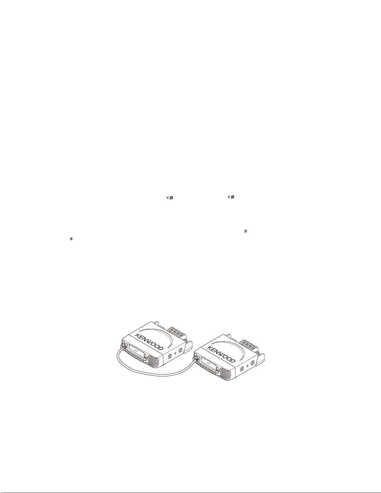
7. Clone Mode
Programming data can be transferred from one transceiver to another by connecting them via their modular
microphone jacks. The operation is as follows (the transmit
transceiver is the source and the receive transceiver is a target). Clone mode should be enabled.
The following data cannot be cloned.
• T uning data
• Embedded message with password
• Model name data
• ESN (Electronic Serial Number) data
Note:
The following data can be cloned.
• Fleet (own)/ID (own) for FleetSync
• Unit ID (own) for NXDN
• ID (own) for MDC-1200
1. Turn the source transceiver power ON with the [
held down (1 second), “CLONE MODE” is displayed on
the LCD.
2. Power on the target transceiver.
3. Connect the cloning cable (No. E30-3382-05) to the mod-
ular microphone jacks on the source and target.
4. Press the [
The data of the source is sent to the target. While the
source is sending data, red LED blinked. While the target
is receiving the data, “PROGRAM” is displayed and green
LED blinked. When cloning of data is completed, the
source displays “END”, and the source red LED turned
off, and the target automatically operates in the User
mode. The target can then be operated by the same pro-
gram as the source.
5. The other target can be continuously cloned. Carry out
the operation in step 2 to 4.
] key on the source transceiver.
] key
模式组合
7. 复制模式
通过模块化麦克风插孔连接车载对讲机,可以将编程数据
从一台传输到另一台。具体操作如下 ( 发射车载对讲机是主
机,接收车载对讲机是子机 )。 应当启用复制模式。
不能复制以下数据。
· 调谐数据
· 带密码的嵌入信息
· 机型数据
· ESN( 电子序列号 ) 数据
注意 :
可以复制以下数据。
· FleetSync 的 Fleet( 自身 )/ID( 自身 )
· NXDN 的 Unit ID( 自身 )
· MDC-1200 的 ID( 自身 )
1. 按住 [
MODE”。
2. 打开子机的电源。
3. 将复制电缆 ( 编号 :E30-3382-05) 连接到主机和子机上的
模块化麦克风插孔。
4. 按主机上的 [
主机的数据便被发送到子机。主机发送数据时,红色 L ED
将会闪烁。子机接收数据时,将显示“PROGRAM”且绿色
LED 闪烁。数据复制完成后,主机显示“END”,主机的红
色 L ED 熄灭,子机自动以用户模式运行。然后子机就可以
按与主机相同的程序操作。
5. 可以继续对另一台子机进行复制。执行步骤 2 至 4 的操作。
] 键 (1 秒 ) 打开主机的电源,LCD 上显示“CLONE
]键。
Cloning cable
E30-3382-05
7-1. How to enter the data password
If the read authorization password is set in the optional
feature menu, you must enter the password (Source transceiver) to activate a clone mode.
You can use 0~9 to confi gure the password. The maximum length of the password is 6 digits.
复制电缆
/
Fig. 2 / 图2
7-1. 如何输入数据密码
如果在可选功能菜单中设置了读取授权密码,则您必须输
入密码 ( 主机 ) 方可激活复制模式。
可使用0~9设置密码。密码最大长度为 6 位。
9
NX-820
REALIGNMENT /
1. [
] + Power ON.
2. “CLONE LOCK” is displayed on the LCD.
3. If the [
displayed, numbers (0 to 9) are displayed fl ashing. When
you press the [
determined. If you press the [
password in this procedure, “CLONE MODE” is displayed
if the entered password is correct. If the password is incorrect, “CLONE LOCK” is redisplayed.
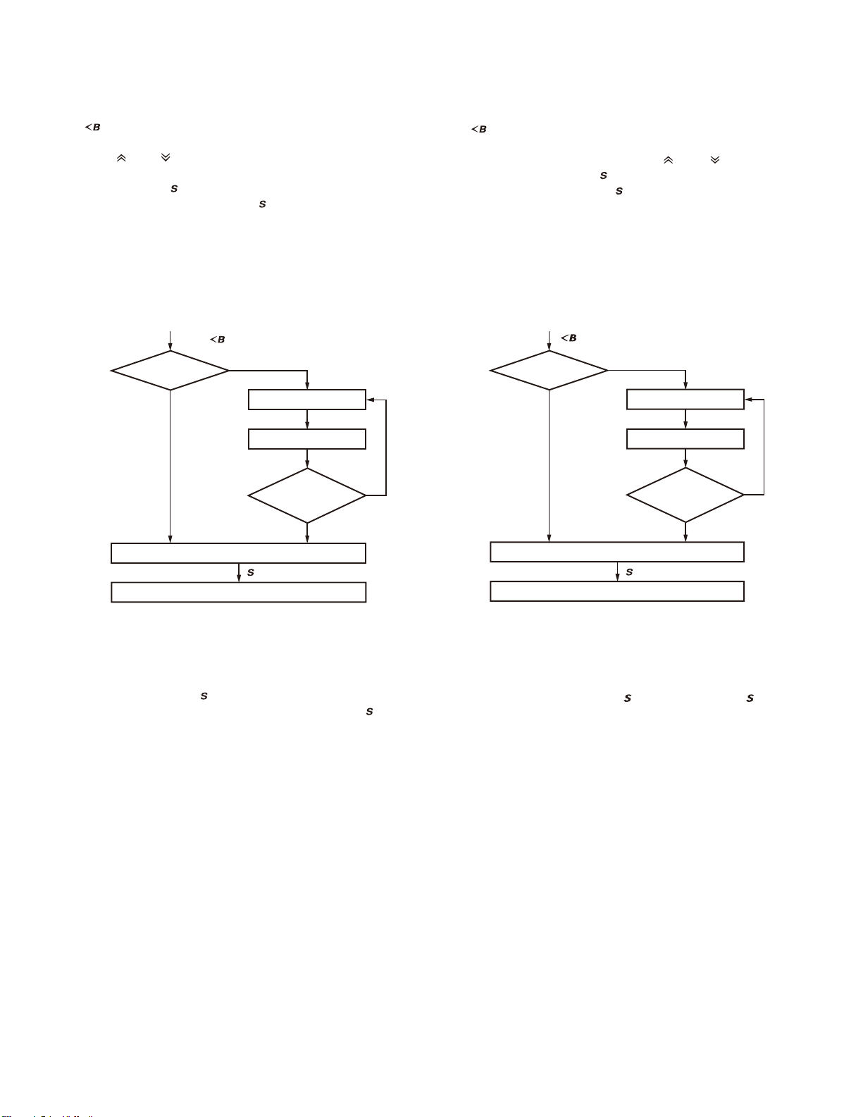
7-2. Flow chart (Source transceiver)
] and [ ] keys is pressed while “CLONE LOCK” is
] key, the currently selected number is
] key after entering the
Press [ ] key + Power ON for 1 second
password*
* Read
Authorization
password
Is
set?
No
Yes
Shows CLONE LOCK
Enter password
模式组合
1. [ ]+ 接通电源。
2. LCD 上显示“CLONE LOCK”。
3. 如果在显示“CLONE LOCK”时按 [
(0 到 9) 闪烁显示。按 [
在此步骤中输入密码后按 [
则显示“CLONE MODE”。如果密码不正确,则重新显示“CLONE
LOCK”。
] 键即可确定当前选择的数字。
] 键,如果输入的密码正确,
7-2. 流程图 ( 主车载对讲机 )
[
] + 打开电源 (1 秒 )
是
了密码 *?
* 读取授权密码
是否设置
否
]和[ ] 键,数字
显示 CLONE LOCK
输入密码
Is entered
password
correct?
Yes
Clone mode
[ ]
Start the clone function
8. Firmware Version Information
Press and hold the [ ] key while turning the transceiver
power ON and then keep pressing and holding the [
the fi rmware version information appears on the LCD.
No
] key,
输入的密码
是否正确 ?
是
复制模式
[ ]
启动复制功能
8. 固件版本信息
打开车载对讲机电源时按住 [ ]键,然后一直按住 [ ]键,
LCD 上便出现固件版本信息。
否
10
NX-820
INSTALLATION /
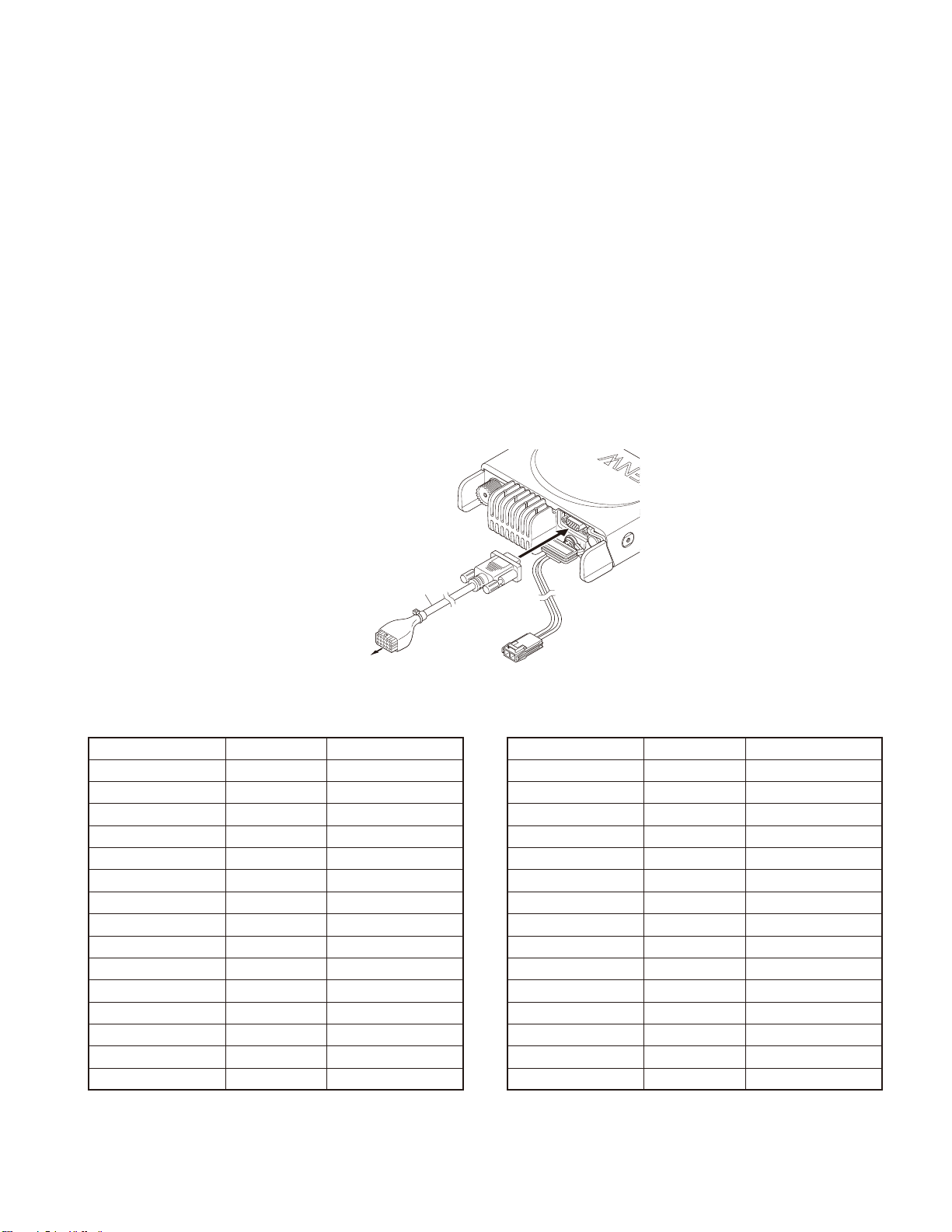
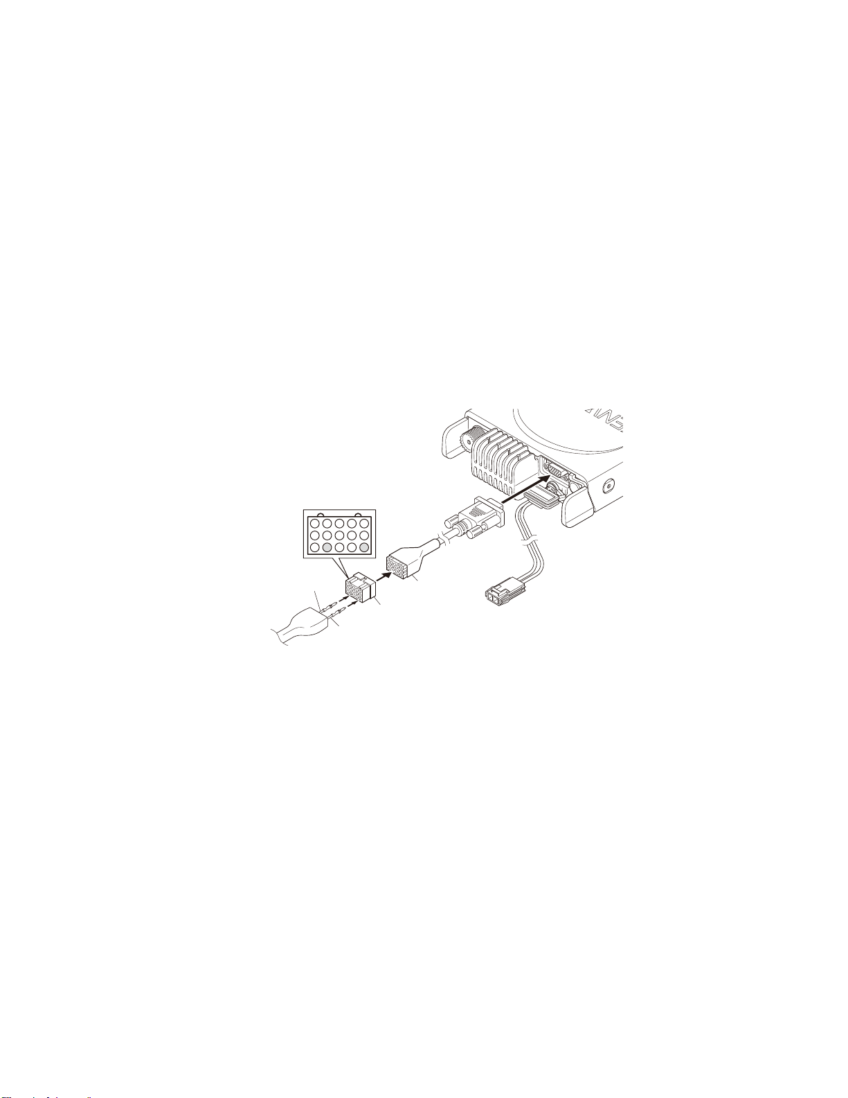
1. Connection Cable (KCT-60: Option)
The KCT-60 connection cable kit is used to connect the
transceiver to a Horn alert cable, KCT-18 (Ignition sense
cable), KES-5 (External speaker), or through the KCT-36 extension cable.
1-1. Installing the KCT-60 (Connection cable) in the
transceiver
1. Remove the ACC. cap on the rear of the transceiver.
2. Connect the D-sub connector of the KCT-60 to the D-sub
15-pin terminal of the transceiver.
3. Connect the 15-pin connector of the KCT-60 to a Horn
alert cable, KCT-18, KES-5, or through a KCT-36 exten-
sion cable.
Note: You must setup using the KPG-141D(C).
安装
1. 连接电缆 (KCT-60: 选购件)
KCT-60 连接电缆组件用于将车载对讲机连接到喇叭提示电
缆、KCT-18 ( 点火感应电缆 )、KES-5 ( 外部扬声器 ),或通
过 KCT-36 延长电缆连接。
1-1. 在车载对讲机上安装 KCT-60 ( 连接电缆 )
1. 拆下车载对讲机后部的 ACC. 盖。
2. 将 KCT-60 的 D-sub 连接器连接到车载对讲机的 D-sub 15
针端子。
3. 将 K CT-60 的 15 针连接器连接到喇叭提示电缆、KCT-18、
KES-5,或通过 KCT-36 延长电缆。
注意 : 必须使用 KPG-141D(C) 进行设置。
KCT-60
Horn alert cable, KCT-18, KES-5 or through KCT-36 extension cable
喇叭提示电缆、KCT-18、KES-5 或通过 KCT-36 延长电缆
1-2. T erminal function
D-sub 15-pin Pin No. Name Molex 15-pin Pin No.
1SB1
2 IGN 2
3 PA or EXT-SP 12
4DO4
5DI5
6 FNC1 9
7 FNC2 11
8 FNC3 7
9 FNC4 6
10 FNC5 8
11 FNC6 10
12 5C 13 HR1 13
14 HR2 14
15 GND 3
1-2. 端子功能
D-sub 15 针针脚号 名称 Molex 15 针针脚号
1SB1
2 IGN 2
3 PA 或 EXT-SP 12
4DO4
5DI5
6 FNC1 9
7 FNC2 11
8 FNC3 7
9 FNC4 6
10 FNC5 8
11 FNC6 10
12 5C -
13 HR1 13
14 HR2 14
15 GND 3
11
NX-820
INSTALLATION /
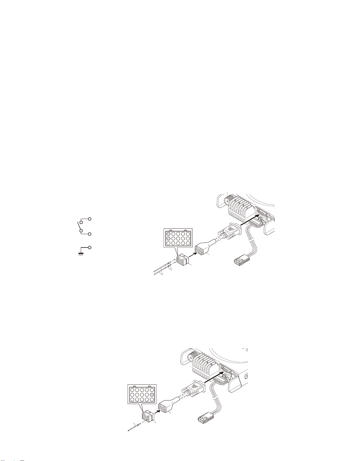
2. Horn Alert Function
The Horn alert function (max. 2A drive) is enabled by in-
stalling the KCT-60 in the transceiver.
2-1. Installation Procedure
1. Remove the ACC. cap on the rear of the transceiver.
2. Connect the D-sub connector of the KCT-60 to the D-sub
15-pin terminal of the transceiver.
3. Insert the two crimp ter minals of the Horn alert cable to
pins 13 and 14 of the square plug.
4. Connect the square plug to the 15-pin connector of the
KCT-60.
5. Connect the remaining two Horn aler t cables to your car
Horn alert signal control. The internal FET switch can be
controlled by turning the HA function on/off and by using
a signaling decode output. The maximum current of HA
is 2A. This switch is the FET switch of P-channel type.
Therefore, a DC power supply is necessary to use the
HR1. The voltage range is from 5V to 16V.
Note: You must setup using the KPG-141D(C).
安装
2. 喇叭提示功能
在车载对讲机上安装 KCT-60,可使用喇叭提示功能 ( 最
大2A驱动)。
2-1. 安装步骤
1. 拆下车载对讲机后部的 ACC. 盖。
2. 将 KCT-60 的 D-sub 连接器连接到车载对讲机的 D-sub 15
针端子。
3. 将喇叭提示电缆的两个压接式端子插入方形插头的针脚 13
和 14。
4. 将方形插头连接到 KCT-60 的 15 针连接器。
5. 将剩下的两条喇叭提示电缆连接到汽车的喇叭提示信号控
制。
内部 FET 开关可通过打开 / 关闭 H A 功能和使用信令解码
输出进行控制。HA 的最大电流为 2A。这个开关是 P 通道
类型的 FET 开关。因此,需 DC 电源方可使用 HR1。电压范
围为 5V 至 16V。
注意 : 必须使用 KPG-141D(C) 进行设置。
13. HR1
14. HR2
3. GND
Horn alert cable
3. Ignition Sense Cable (KCT-18: Option)
The KCT-18 is an optional cable for enabling the ignition
function. The ignition function lets you turn the transceiver
power on and off with the car ignition key.
3-1. Installing the KCT-18 (Ignition sense cable) in
the transceiver
13
10
7
4
14
15
1
11
8
5
2
12
9
6
3
13
14
Crimp terminal
KCT-60
Square plug
压接式端子
/
喇叭提示电缆
/
方形插头
/
3. 点火感应电缆 (KCT-18: 选购件)
KCT-18 为用于启用点火功能的选购电缆。点火功能让您能
够通过汽车点火钥匙打开和关闭车载对讲机的电源。
3-1. 在车载对讲机上安装 KCT-18 ( 点火感应电缆 )
12
7
10
13
8
11
14
9
12
15
KCT-18
Ignition line of the car
2
1
4
2
5
3
6
Square plug
汽车点火线
/
KCT-60
方形插头
/
NX-820
INSTALLATION /
4. External Speaker (Option)
4-1. KES-5
External speaker KES-5 can be installed for KCT-60.
Connection procedure
■
1. Remove the ACC. cap on the rear of the transceiver.
2. Connect the D-sub connector of the KCT-60 to the D-sub
15-pin terminal of the transceiver.
3. Insert the two crimp terminals of the KES-5 to pins 3 and
12 of the square plug.
4. Connect the square plug to the 15-pin connector of the
KCT-60.
Note:
You must set up using the KPG-141D(C).
Before the external speaker can be used, you must as-
sign one of the keys as “External Speaker”, using the
KPG-141D(C).
安装
4. 外部扬声器 ( 选购件)
4-1. KES-5
外部扬声器 KES-5 可安装于 KCT-60。
■ 连接步骤
1. 拆下车载对讲机后部的 ACC. 盖。
2. 将 KCT-60 的 D-sub 连接器连接到车载对讲机的 D-sub 15
针端子。
3. 将 KES-5 的两个压接式端子插入方形插头的针脚3和12。
4. 将方形插头连接到 KCT-60 的 15 针连接器。
注意 :
必须使用 KPG-141D(C) 进行设置。
必须使用 K P G -141D(C) 将某个键指定为“外部扬声器”,
方可使用外部扬声器。
13
10
7
4
11
8
12
9
12
Black lead
1
5
2
6
3
3
Square plug
黑色导线
/
Black/White lead
黑色 / 白色导线
14
15
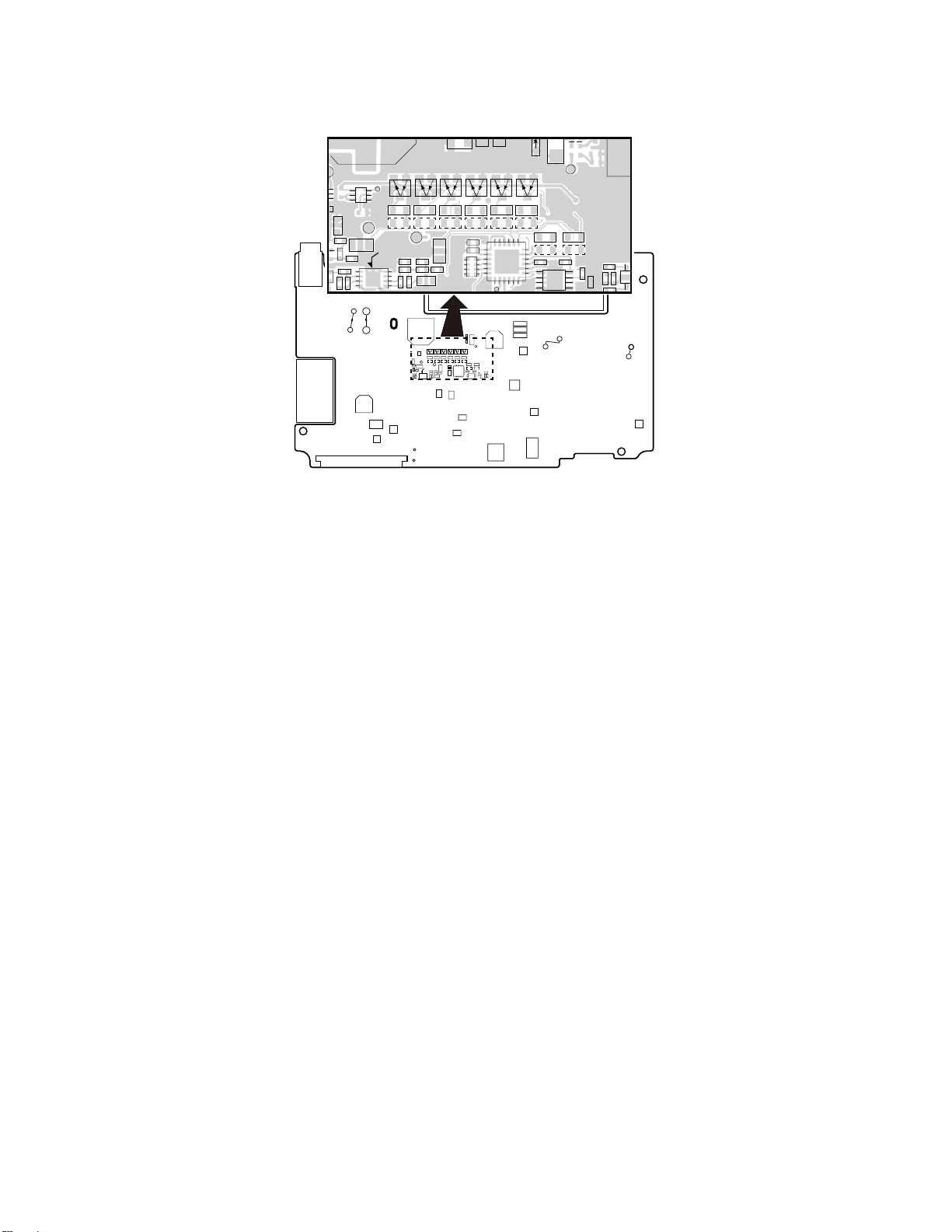
5. Changing Serial Port Level
5-1. Change FNC1 (TXD) and FNC2 (RXD) of D-SUB
15-pin connector from TTL level to RS-232C
level
FNC1 (TXD /6pin ) and FNC2 (RXD /7pin ) of D-SUB 15pin connector are confi gured at the TTL level as the default
value. But you can change these serial port level to RS232C level through the RS-232C level converter IC (IC516)
by confi guring the port.
Remove the R664, R635 and R662 chip jumpers and solder the chip jumpers to R666, R633 and R665.
5-2. Change FNC1 (TXD), FNC2 (RXD), FNC3 (RTS)
and FNC4 (CTS) of D-SUB 15-pin connector
from TTL level to RS-232C level
FNC1 (TXD/6pin), FNC2 (RXD/7pin), FNC3 (RTS/8pin)
and FNC4 (CTS/9pin) of D-SUB 15-pin connector are configured at the TTL level as the default value. But you can
change these serial port level to RS-232C level through the
RS-232C level converter IC (IC516) by confi guring the port.
Remove the R664, R635, R662, R659, R658 and R632
chip jumpers and solder the chip jumpers to R666, R633,
R665, R663, R660 and R630.
KCT-60
方形插头
/
5. 改变串行接口电平
5-1. 将 FNC1 (TXD) 和 FNC2 (RXD) 的 D-SUB 15 针连接
器从 TTL 电平转换到 RS-232C 电平
FNC1 (TXD/6针)和FNC2 (RXD/7针)的D-SUB 15 针连
接器被默认设置在 TTL 电平。但可以通过端口设置将这些串
行端口电平通过 RS-232C 档位转换器 IC (IC516) 转换至 RS232C 电平。
从 R664,R635 和 R662 跳线至 R666,R633 和 R665。
5-2. 将 D-SUB 15 针连接器的 FNC1 (TXD),FNC2 (RXD),
FNC3 (RTS) 和 FNC4 (CTS) 从 TTL 电平转换到 RS232C 电平
D-SUB 15 针连接器的 FNC1 (TXD/6 针 ),FNC2 (RXD/7 针 ),
FNC3 (RTS/8针)和FNC4 (CTS/9 针 ) 默认设置在 TTL 电平。
但可以通过端口设置将这些串行端口电平通过 RS-232C 档位
转换器 IC (IC516) 转换至 RS-232C 电平。
从 R664,R635,R662, R659, R658 和 R632 跳 线 至 R666,
R633,R665,R663,R660 和 R630。
13
NX-820
INSTALLATION /
+
R635
R664
5
R633
R666 R665
6
IC703
R664
5
6
IC703
R635
R662
R662
R658
R659
R663
R658
R659
R632
15
16
R632
R660
R630
R797R796
19
20
安装
15
16
R797
R796
R798
TX-RX unit
Component side
收发单元
元件面
R799
19
20
In the case of 5-1.
■
[TTL level]
R664,R635 and R662: 0 chip jumper.
R666, R633 and R665: open.
[RS-232C level]
R666, R633 and R665: 0 chip jumper.
R664, R635 and R662: open.
In the case of 5-2.
■
[TTL level]
R664, R635, R662, R659, R658 and R632: 0 chip
jumper.
R666, R633, R665, R663, R660 and R630: open.
[RS-232C level]
R666, R633, R665, R663, R660 and R630: 0 chip
jumper.
R664, R635, R662, R659, R658 and R632: open.
6. Changing of Signal Type
6-1.Change signal output of D-SUB connector
from DEO to AFO
The output (4pin) of D-SUB 15-pin connector is confi g-
ured at the DEO as the default value.
Remove the R796 chip jumper and solder the clip jumper
to R798.
■ 5-1 的场合
[TTL 电平 ]
R664,R635 和 R662: 0贴片电阻。
R666,R633 和 R665: 断开。
[RS-232C 电平 ]
R666,R633 和 R665: 0贴片电阻。
R664,R635 和 R662: 断开。
■ 5-2 的场合
[TTL 电平 ]
R664,R635,R662,R659,R658 和 R632: 0贴片电阻。
R666,R633,R665,R663,R660 和 R630: 断开。
[RS-232C 电平 ]
R666,R633,R665,R663,R660 和 R630: 0贴片电阻。
R664,R635,R662,R659,R658 和 R632: 断开。
6. 改变信号类型
6-1. 请将 D-SUB 连接器的信号输出从 DEO 变更到 AFO。
D-SUB 15 针连接器的输出 (4 针 ),作为默认值形成 DEO。
从 R796 跳线至 R798。
6-2. Change signal input of D-SUB connector from
DI to MI2
The input (5pin) of D-SUB 15-pin connector is confi gured
at the DI as the default value.
Remove the R797 chip jumper and solder the chip jump-
er to R799.
14
6-2. 请将 D-SUB 连接器的信号输入从 DI 变更到 MI2。
D-SUB 15 针连接器的输入 (5 针 ),作为默认值形成 DI。
从 R797 跳线至 R799。
NX-820
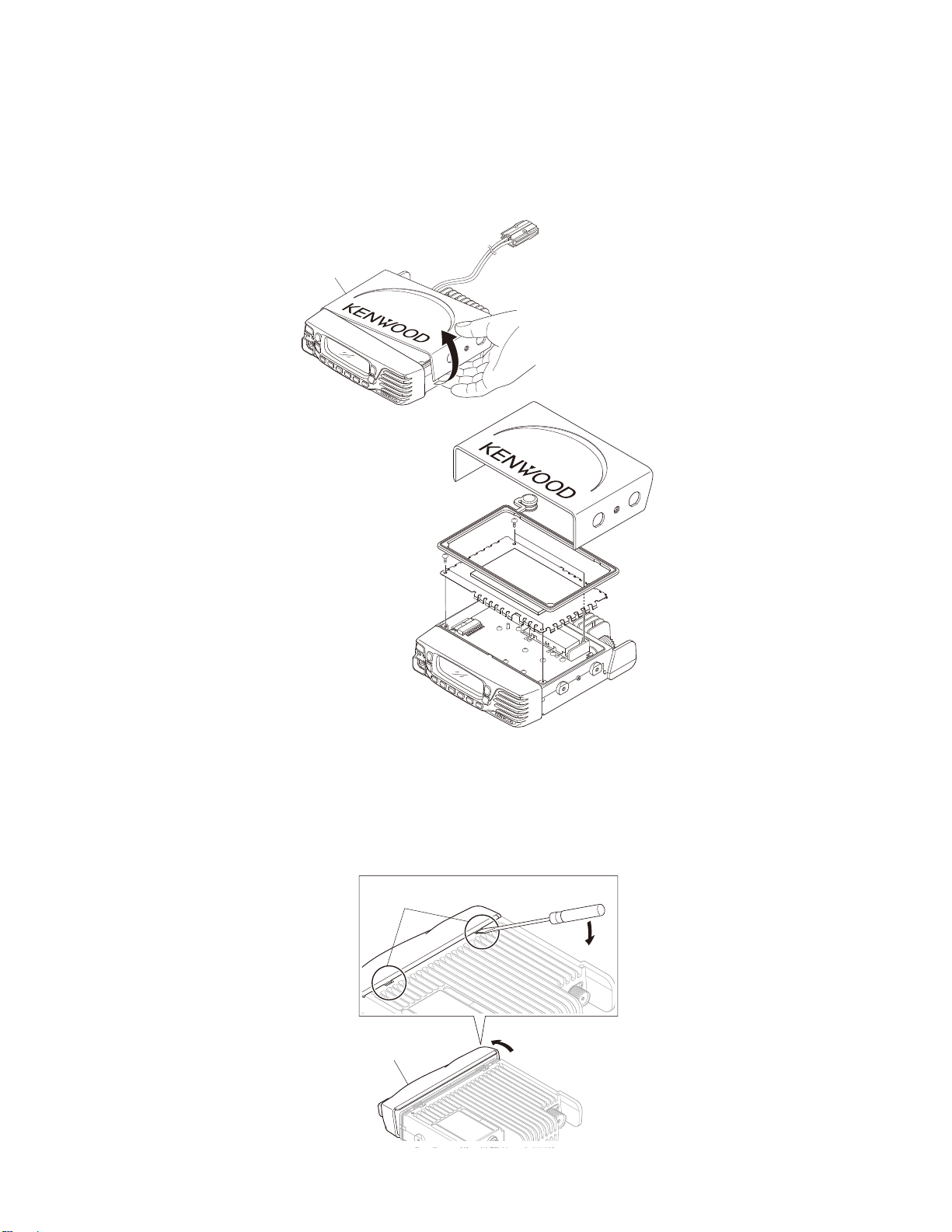
DISASSEMBLY FOR REPAIR /
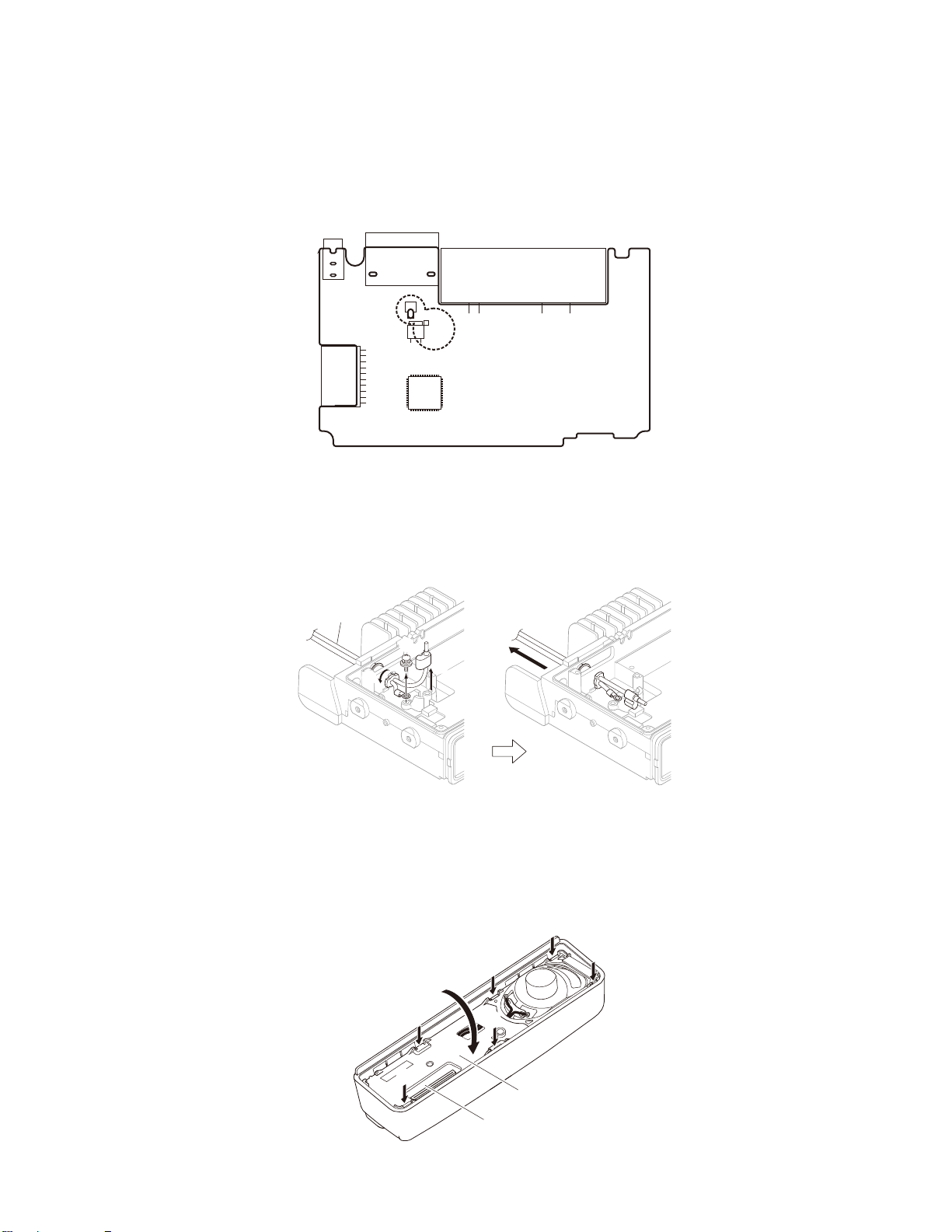
1. Disassembly Procedure
1. Remove the cabinet, top packing and shielding plate of
the transceiver.
Cabinet
机壳
/
维修拆卸
1. 拆卸步骤
1. 取下车载对讲机的机壳、顶盖和屏蔽板。
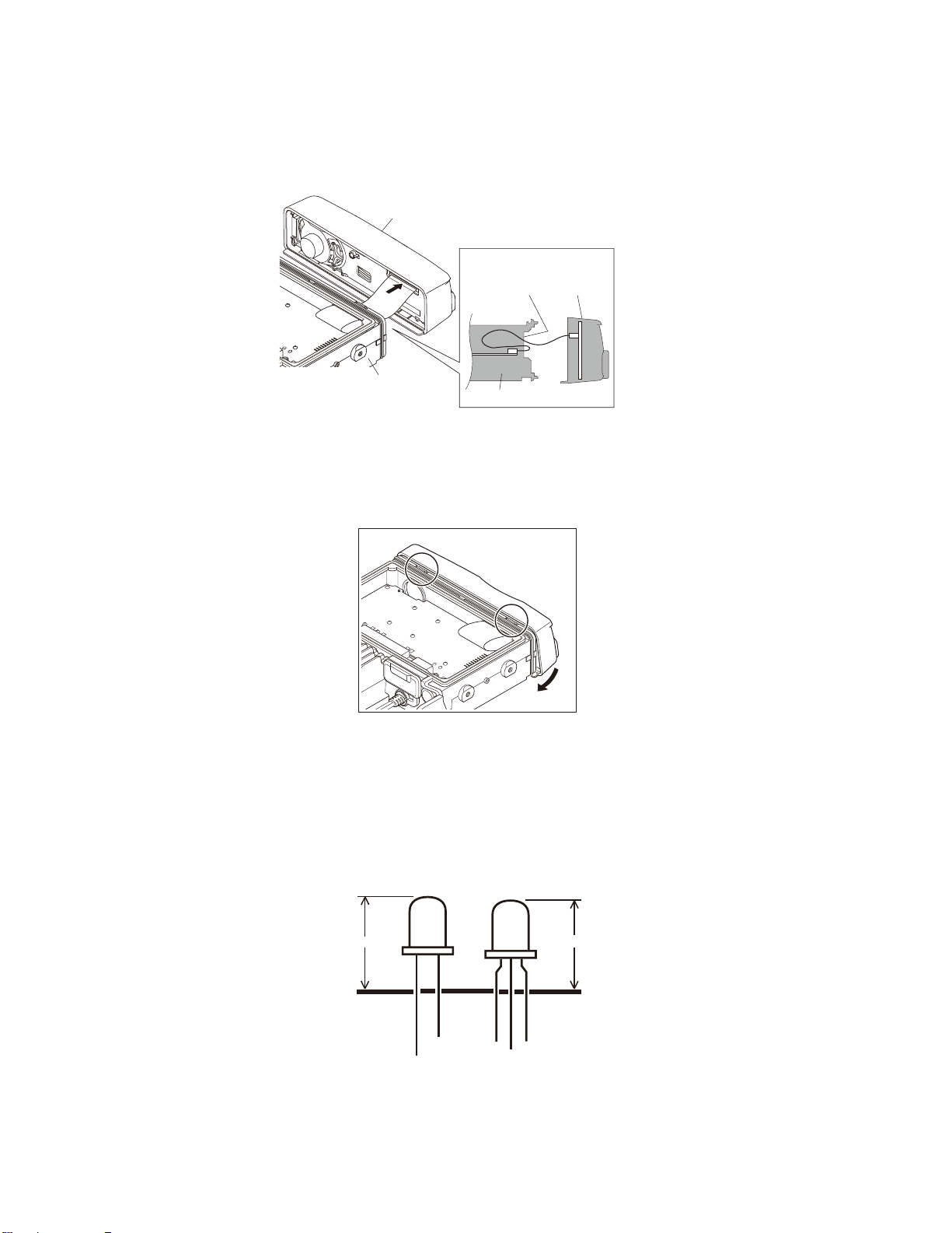
2. To remove the panel assembly, fi rst turn the transceiver
upside down.
Then, insert a fl at-head screwdriver into the holes of the
chassis and tilt it in the direction as shown by the arrow.
Holes
孔
/
Panel assembly
面板组件
2. 要拆卸面板组件,应先将车载对讲机颠倒放置。
然后,将一字螺丝刀插入底座的孔内,使其按箭头所示的
方向倾斜。
15
NX-820
DISASSEMBLY FOR REPAIR /
3. Disconnect the fl at cable from connector of the panel assembly.
4. Hook the finger to hole and while pulling the speaker
holder to this side, expand the panel side of a to c, and
remove the speaker holder from the front panel.
维修拆卸
3. 从面板组件的连接器断开带状电缆。
Flat cable
带状电缆
4. 拇指放入如图所示的洞孔中,然后同时拉起扬声器座和拉
开面板的①到③处,就可以从面板上卸下扬声器座。
b
a
c
Speaker holder
扬声器座
5. When removing the TX-RX PCB, first remove the top
packing.
Then, remove the solder of the antenna hot pin and posi-
tive terminal of the DC cord.
Remove the 16 screws from the TX-RX PCB, power mod-
ule, and audio amp.
Positive terminal of
the DC cord
直流电源线的正极端子
Audio amp
音频放大器
5. 拆卸收发 PCB 时,应先拆下顶盖。
然后,除去天线热端和直流电源线的正极端子的焊锡。
拆下收发 PCB、功率模块和音频放大器上的 16 颗螺丝。
Antenna hot pin
天线热端
16
TX-RX PCB
收发 PCB
Power module
功率模块
Top packing
顶盖
NX-820
DISASSEMBLY FOR REPAIR /
Note:
When you supply power to the TX-RX PCB after remov-
ing the TX-RX PCB from the chassis, solder the positive
and ground terminals of the DC cord (Recommendation:
E30-3448-25) to the + and GND terminals of the TX-RX
PCB.
+
GND
6. Pull it out behind the chassis by rotating the bush c of
the DC cord 90 degrees in the direction of the arrow after
the screw a in the negative terminal is removed, and the
positive terminal b is removed from the chassis.
维修拆卸
注意 :
从底座上拆下收发 PCB 之后对收发 PCB 供电时,将直流电
源线 ( 推荐 : E30-3448-25) 的正极和接地端子焊接到收
发PCB的+和GND端子。
TX-RX PCB
Component side
6. 拆下负极端子的螺丝①,并从底座上拆下正极端子②之后,
将直流电源线的套管③以箭头方向旋转 90 度,将其拉出
至底座后面。
收发 PCB
/
元件面
/
DC cord
直流电源线
a
c
b
2. Precautions for Reassembly
1. The tab from a to c is applied the front panel fi rst. And,
to f tabs inside the front panel is pushed.
d
c
2. 重新组装注意事项
1. 首先放下①到③的凸起部 , 然后再按住④到⑥的凸起部。
b
e
a
d
f
Speaker holder
扬声器座
Display PCB
显示 PCB
17
NX-820
DISASSEMBLY FOR REPAIR /
2. When mounting the panel assembly, pass the fl at cable
through the hole of the chassis as shown below then connect the fl at cable to connector of the panel assembly.
Panel assembly
面板组件
Chassis
底座
3. Fit the panel assembly into the two tabs of the chassis
top side fi rst.
Then, fit the panel assembly into the two tabs of the
chassis bottom side by turning the panel assembly.
维修拆卸
2. 安装面板组件时,如下图所示将带状电缆穿过底座的孔,
然后将带状电缆连接到面板组件的连接器。
Hole of
the chassis
底座的孔 面板组件
Chassis
3. 先将面板组件装配到底座顶侧的两个凸起内。然后,再通
Panel
assembly
底座
/
过转动面板组件,将面板组件装配到底座底侧的两个凸起
内。
3. Correspondence when replacing the
LED (D22 and D23)
When replacing the LED (D22 and D23), it makes it to
length.
13mm
18
LED
D22
3. 更换 LED (D22 和 D23) 时的相应操作
更换 LED (D22 和 D23) 时,将 LED 的引线截到如下图所的
尺寸。
LED
D23
12mm
NX-820
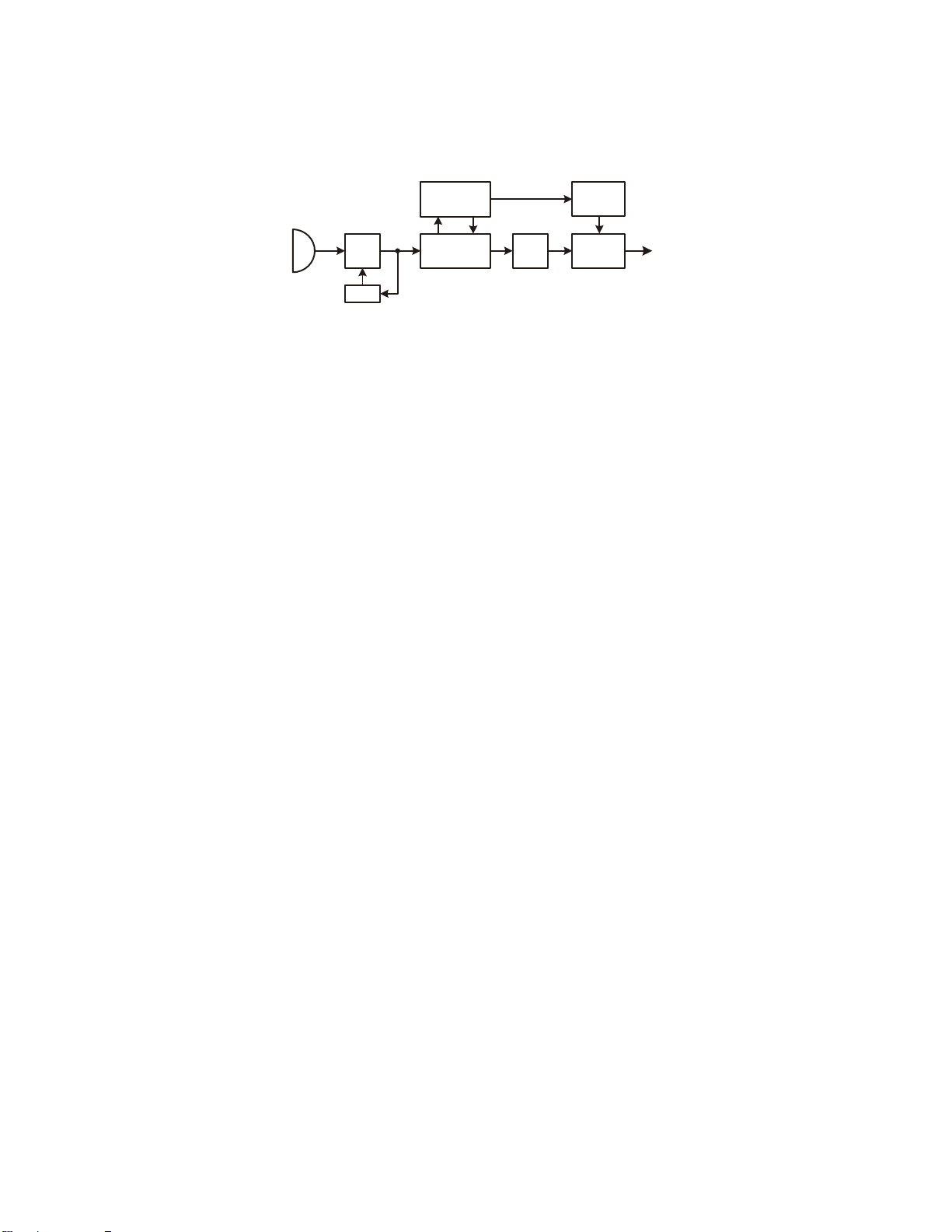
CIRCUIT DESCRIPTION /
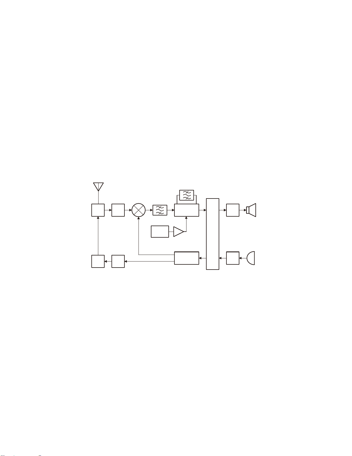
1. Overview
The NX-820 is a UHF Mobile transceiver designed to
operate in the frequency range of 400 to 470MHz. The unit
consists of a receiver, transmitter, phase-locked loop (PLL)
frequency synthesizer, baseband parts, power supply, and
control circuits.
2. Frequency Confi guration
The receiver is a double-conversion super-heterodyne
using the fi rst intermediate frequency (IF) of 49.95MHz and
the second IF of 450kHz. Incoming signals from the antenna are mixed with the local signal from the PLL circuit to
produce the fi rst IF of 49.95MHz. This is then mixed with
the 50.4MHz second local oscillator output to produce the
450kHz second IF. The transmit signal frequency is generated by the PLL VCO, and modulated by the signal from the
DSP. It is then amplifi ed and fed to the antenna.
ANT
TX/RX : 400~470MHz
MCF
49.95MHz
ANT
SW
RF
AMP
1st MIX
电路说明
1. 概述
NX-820 为 UHF 车载对讲机,设计用于 400 至 470MHz 的频
率范围。该设备由接收机、发射机、锁相环 (PLL) 频率合成
器、基带部件、电源和控制电路组成。
2. 频率构成
接收机为二次变频超外差方式,使用的第一中频 (IF) 为
49.95MHz,第二中频为 450kHz。天线接收到的信号与 PLL 电
路的本振信号混频,从而产生第一个 49.95MHz 的中频。然
后与第二个 50.4M H z 的本地振荡器输出信号混频,进而产生
第二个 450kHz 的中频。发射的信号频率由 PL L VC O 生成,
并经 DSP 信号调制。最后,该信号频率经过放大并发送到天线。
CF
450kHz
SP
MIX
IF AMP
AF
AMP
16.8MHz
TCXO
350.05~
420.05MHz
PA
AMP
TX
AMP
400~470MHz
Fig.1 Frequency confi guration / 图 1 频率构成
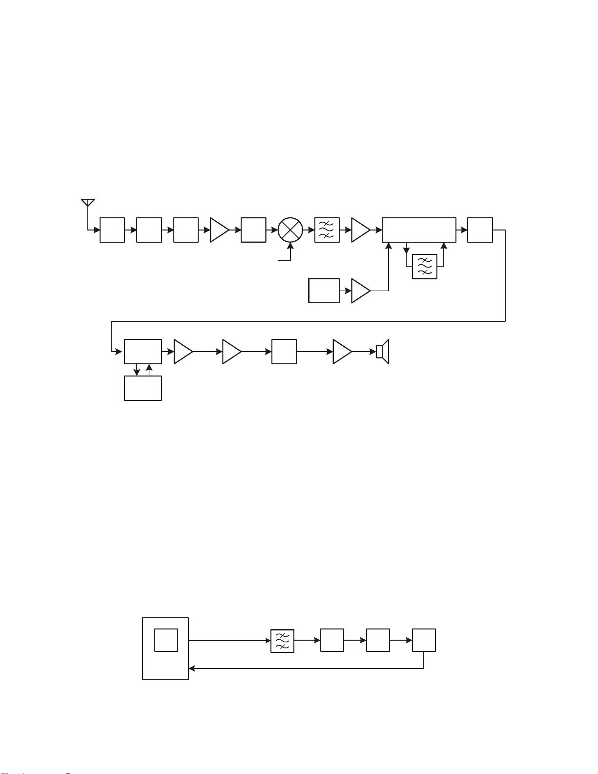
3. Receiver System
3-1. RF circuit
An incoming RF signal from the antenna terminal is
passed through the antenna switch (D110, 111 and 107) and
then the bandpass fi lter (L215, 216 and 210). The bandpass
fi lter is adjusted by a variable capacitor. The input voltage to
the variable capacitor is regulated by the voltage output from
the D/A converter (IC712). The signal is amplifi ed by an RF
amplifier (Q202), and passed through the bandpass filter
(L207, 208, 209 and 211). The resulting signal is applied to
the fi rst mixer (Q201) where it is mixed with the fi rst local
oscillator signal output from the frequency synthesizer to
produce the fi rst IF (49.95MHz).
3-2. IF circuit
The fi rst IF signal is passed through a four-pole monolithic crystal fi lter (XF1) to reject the adjacent channel signal.
The fi ltered fi rst IF signal is amplifi ed by the fi rst IF amplifi er
(Q305) and then applied to the IF system IC (IC303). The
IF system IC provides a second mixer, AGC amplifi er , and
RSSI (Received Signal Strength Indicator).
×
3
50.4MHz
MIC
PLL
VCO
Baseband Circuit
MIC
AMP
3. 接收部系统
3-1. RF 电路
天线端子接收到的 RF 输入信号依次通过天线开关 (D110、
111 和 107) 和带通滤波器 (L215、216 和 210)。带通滤波
器经由可变电容器调整。可变电容器的输入电压经由数模转
换器 ( I C712) 的输出电压进行调整。随后,信号被 RF 放大
器 ( Q202) 放大,然后通过带通滤波器 ( L207、208、209 和
211)。最终的信号被运用到第一混频器 (Q201)。在该混频器
中,信号与频率合成器输出的第一本地振荡器信号混频,从
而产生第一中频 (49.95MHz)。
3-2. 中频电路
第一中频信号经过一个四极单片晶体滤波器 (XF1) 以消除
临近信道的信号。滤波后的第一中频信号经过第一中频放大
器 (Q305) 的放大后,加载到中频系统 IC (IC303) 上。中频
系统 IC 提供一个第二混频器、AGC 放大器和 RSSI ( 接收信号
强度指示器 )。
19
NX-820
CIRCUIT DESCRIPTION /
The second mixer mixes the first IF signal with the
50.4MHz of the second local oscillator output and produces
the second IF signal of 450kHz.
The second IF signal is passed through the ceramic fi lter
(CF1) to reject the adjacent channel signal. The fi ltered second IF signal is amplifi ed by the AGC amplifi er.
The signal from the AGC amplifi er is input to the ASIC
(IC507) through the ceramic fi lter (CF2).
ANT
L116, 117
LPF
110,111
D
D107
ANT
SW
IC507
ASIC
L215
IC711
,
216
210
BPF
(1/2)
,
Q202
RF AMP
IC711
(2/2)
L207,208
L209,211
BPF
1st PLL
OSC(PLL)
Q201
1st MIX
IC712
VOL
电路说明
第二混频器混合第一中频信号及 50.4M H z 的第二本地振荡
器输出,生成 450kHz 的第二中频信号。
第二中频信号通过陶瓷滤波器 (CF1) 以消除临近信道的信
号。滤波后的信号由 AGC 放大器进行放大。
AGC 放大器的信号通过陶瓷滤波器 (CF2) 被输入 ASIC
(IC507)。
XF1 Q 305
MCF IF AMP
X1
TCXO
16.8MHz
IC714
Q303
x
IC303
MIX , AGC
2nd OSC
3
CF1
SP
CF2
BPF
IC502
DSP
Fig.2 Receiver System / 图 2 接收机系统
3-3. Audio amplifi er circuit
Audio processing (high-pass filter, low-pass filter, deemphasized and so on) in FM mode and decoding in NXDN
mode are processed by the DSP (IC502). Audio signals from
the ASIC (IC507), IC502 goes through the amplifi er (IC711).
The signal then goes through the D/A converter (IC712) and
an amplifi er (IC714).
3-4. Squelch circuit
It amplifies the demodulated noise signal from ASIC
(IC507) after fi ltering through the LPF and HPF circuit. The
amplifi ed signal is then converted to a DC signal by the detection circuit. The converted signal is fed back to IC507.
IC705 (1/ 2)
DET
IC507
ASQAPC
ASQDET
3-3. 音频放大器电路
FM 模式的音频处理 ( 高通滤波器、低通滤波器、去加重等 )
和 NXDN 模式的解码由 DSP (IC502) 进行处理。ASIC (IC507)
和 I C502 的音频信号通过放大器 (IC711)。然后信号通过数
模转换器 (IC712) 和放大器 (IC714)。
3-4. 静噪电路
通过 L P F 和 HPF 电路滤波后,该电路放大 ASIC (IC507)
的已解调噪音信号。随后,放大的信号由检测电路转换为 DC
信号。转换的信号被反馈给 IC507。
Q702 D702
AMP RECT
ASQ
IC705 (
AMP
2)
2
/
20
Fig. 3 Squelch Circuit / 图 3 静噪电路
NX-820
CIRCUIT DESCRIPTION /
4. T ransmitter System
MIC
IC703 (2/2)
AMP
AGC
D703,704
Q703,704
Fig. 4 Transmitter System / 图 4 发射机系统
4-1. Audio Band Circuit
The signal from the microphone is amplifi ed by IC703 (1/2)
and limited by the AGC circuit composed of D703, D704,
Q703 and Q704. IC703 (2/2) works as an anti-aliasing LPF
fi lter.
4-2. Baseband Circuit
The audio signal output from the Audio band circuit is
converted to digital data with a sampling frequency of 48
kHz. This digital data is sent to the DSP (IC502), and voice
signals of 300Hz or lower and frequencies of 3kHz or higher
are cut off so that an audio range 300Hz to 3kHz is extracted. The audio signal is then pre-emphasized in FM mode
and synthesized with the signals, such as QT and DQT, as
required, and is then output from the ASIC (IC507). In Digital mode, the audio signal is converted to the 4-Level FSK
baseband signal and is output from IC507. The DTMF and
MSK baseband signals are also generated by the DSP and
output from IC507.
LPF (IC701) works as smoothing fi lter. The output level
according to the transmit carrier is fi ne-adjusted according to
each modulation method.
IC502
DSP
IC507
ASIC
电路说明
4. 发射机系统
IC2
PLLIC
IC701(1/ 2)
LPF
VCO
4-1. 音频频带电路
麦克风信号被 IC703 (1/2) 放大并被 D703、D704、Q703
和 Q704 组 成的 A G C 电路所限制。IC703 (2/2) 用作抗混叠
LPF 滤波器。
4-2. 基带电路
从音频频带电路输出的音频信号被转换为取样频率为
48kHz 的数字数据。该数字数据被发送给 DSP (IC502),
300Hz 或更低的语音信号以及 3k H z 或更高的频率被截止,并
选取 300H z 至 3k H z 的音频范围。然后,音频信号以 FM 模
式预加重,并与所需的 QT 和 DQT 等信号合成,然后从 ASIC
(IC507) 输出。在数字模式下,音频信号被转换为4级FSK
基带信号并从 IC507 输出。DTMF 和 MSK 基带信号也由 DSP 生
成并由 IC507 输出。
LPF (IC701) 用作平滑滤波器。根据各自的调制方式对按
照发射载波输出的电平进行微调。
To TX
stage
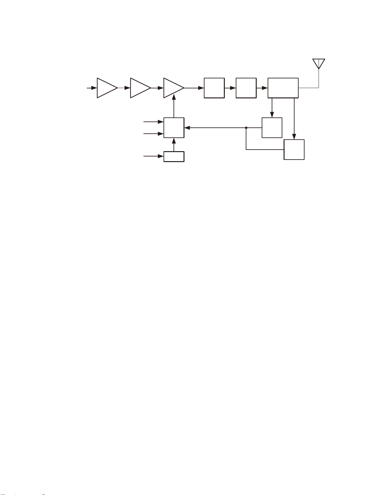
4-3. Drive and Final amplifi er
The signal from the T/R switch (D17 is on) is amplifi ed
by the drive amplifier (Q102) to 16~17dBm. The output of
the drive amplifi er is amplifi ed by the fi nal amplifi er module
(IC102) to 25W (5.0W when the power is low). The output
of the fi nal amplifi er module is then passed through the harmonic fi lter (LPF) and antenna switch (D110, D111 are on)
and directional coupler and is applied to the antenna terminal.
4-4. APC circuit
The Automatic transmission power control (APC) circuit
stabilizes the transmitter output power at a predetermined
level by detecting the power module output with the directional coupler and diode detector (D104 and D105). The diode detector (D104 and D105) applies the detected voltage
to the DC amplifi er IC103 (2/2).
The APC circuit is confi gured to protect over-current of
the power module due to fl uctuations of the load at the antenna end and to stabilize transmission output at voltage and
temperature variations.
4-3. 驱动器和末级放大器
T/R 开关 (D17 开启 ) 的信号由驱动放大器 ( Q102) 放大
到 16 ~ 17dBm。驱动放大器的输出信号由末级放大器模块
(IC102) 放大到 25W ( 当功率低为 5.0W 时 )。末级放大器模
块的输出信号随即通过谐波滤波器 (LPF) 及天线开关 (D110、
D111 开启 ) 及方向性耦合器,然后加载到天线端子上。
4-4. APC 电路
通过使用方向性耦合器和二极管 (D104 和 D105) 检测功
率模块输出,自动发射功率控制 (APC) 电路将发射器输出功
率稳定在预定电平。二极管 (D104 和 D105) 对直流放大器
IC103 (2/2) 施加电压。
配置 A PC 电路是为了保护因天线端负载波动而引起的功率
模块过流,以及在电压和温度变化时稳定发射输出。
21
NX-820
CIRCUIT DESCRIPTION /
Q101
From T/ R SW
D17
Pre
DRIVE
5. PLL Frequency Synthesizer
5-1. TCXO (X1)
The TCXO (X1) generates a reference frequency of
16.8MHz for the PLL frequency synthesizer. This reference
frequency is applied to pin 9 of the PLL IC (IC2) and is connected to the IF circuit as a 2nd local signal through the Tripler.
The frequency adjustment is achieved by switching the
ratio of the dividing frequency. The resolution of the adjusting
frequency is approximately 4Hz.
Q102
DRIVE
80T
MP
/H_L
IC102
FINAL
Gate
bias
APC
DC SW
Fig. 5 APC Circuit / 图 5 APC 电路
IC103
Q105
电路说明
ANT
D107,110,111
ANT
SW
5. PLL 频率合成器
5-1. TCXO (X1)
TCXO (X1) 生成 16.8MHz PLL 频率合成器的基准频率。该
基准频率作为第 2 本振信号通过三倍频器,被加载到 PLL IC
(IC2) 的第 9 脚并送至 IF 电路。
通过切换分频比进行频率调整。调整频率的分辨率约为
4Hz。
ANT
LPF
CPL
D105
For
DET
D104
Rev
DET
5-2. VCO
There is an RX VCO and a TX VCO.
The TX VCO (Q6) generates a transmit carrier and the
RX VCO (Q5) generates the 1st local signal. For the VCO
oscillation frequency, the transmit carrier is 400 to 470 MHz
and the 1st local signal is 350.05 to 420.05MHz.
The VCO oscillation frequency is determined by one system of operation switching terminal "T/R" and two systems
of voltage control terminals "CV" and "ASSIST".
The operation switching terminal, "T/R", is controlled by
the control line (/T_R) output from the ASIC (IC507). When
the /T_R logic is low, the VCO outputs the transmit carrier
and when it is high, it outputs the 1st local receive signal.
The voltage control terminals, "CV" and "ASSIST", are
controlled by the PLL IC (IC2) and ASIC (IC507) and the
output frequency changes continuously according to the
applied voltage. For the modulation input terminal, "VCO_
MOD", the output frequency changes according to the applied voltage. This is used to modulate the VCO output.
"VCO_MOD" works only when "/T_R" is low.
5-3. PLL IC (IC2)
The PLL IC compares the differences in phases of the
VCO oscillation frequency and the TCXO reference frequency, returns the difference to the VCO CV terminal and
realizes the "Phase Locked Loop" for the return control. This
allows the VCO oscillation frequency to accurately match
(lock) the desired frequency.
5-2. VCO
设有一个 RX VCO 和一个 TX VCO。
TX VCO (Q6) 生成发射载波,RX VCO (Q5) 生成第 1 本振
信号。对于 VCO 震荡频率,发射载波为 400 至 470MHz,第 1
本振信号为 350.05 至 420.05MHz。
VCO 震荡频率由一个操作切换端子“T/R”系统和两个电压
控制端子“CV”和“ASSIST”系统确定。
操作切换端子“T/R”由 ASIC (IC507) 控制线路 (/T_R)
的输出信号进行控制。/T_R逻辑低时,VCO 输出发射载波 ;
高时,输出第 1 本振接收信号。
电压控制端子“CV”和“ASSIST”由PLL IC (IC2) 和
ASIC (IC507) 控制,输出频率根据加载的电压持续改变。对
于调制输入端子“VCO_MOD”,输出频率根据加载的电压改变。
籍此调制 VCO 输出。“VCO_MOD”仅在“/T_R”低时工作。
5-3. PLL IC (IC2)
PLL IC 对比 VCO 震荡频率和 TCXO 基准频率的相位差,将
相位差返回至 VCO CV 端子,从而实现反馈控制的“锁相环路”。
这样可以使 VCO 震荡频率与所需的频率精确匹配 ( 锁定 )。
22
NX-820
CIRCUIT DESCRIPTION /
When the frequency is controlled by the PLL, the frequency convergence time increases as the frequency difference increases when the set frequency is changed. To
supplement this, the ASIC (IC507) is used before control by
the PLL IC to bring the VCO oscillation frequency close to
the desired frequency. As a result, the VCO CV voltage does
not change and is always stable at approximately 2.5V.
The desired frequency is set for the PLL IC by the ASIC
(IC507) through the 3-line "SDO1", "P_SCK1", "/PCS_RF"
serial bus. Whether the PLL IC is locked or not is monitored
by the ASIC through the “PLD” signal line. If the VCO is not
the desired frequency (unlocked), the "PLD" logic is low.
The modulation signal of the Low-speed-Data is applied
to pin 23 of the PLL IC (IC2).
The modulation signal that is digital data of a sampling
frequency of 96 kHz is set for the PLL IC by the DSP (IC502)
through the “PLL_MOD” line.
5-4. Local Switch (D16, D17)
The connection destination of the signal output from the
buffer amplifi er (Q11) is changed with the diode switch (D17)
that is controlled by the transmission power supply, HSW,
and the diode switch (D16) that is controlled by the reception
power supply, 50R. If the HSW logic is high, it is connected
to a transmit-side drive (Q102). If the HSW logic is low, it is
connected to a receive-side mixer (Q202).
电路说明
频率由 P LL 控制时,频率锁定时间将随着设定频率改变时
频率差的增大而增加。为对此进行补充,在由 PLL IC 控制之
前使用 ASIC (IC507) 以使 VCO 震荡频率接近所需的频率。因
此,VCO CV 的电压不变,始终稳定在约 2.5V。
PLL IC 的所需频率由 ASIC (IC507) 通过 3 线“SDO1”、“P_
SC K1”、“/PCS_RF”串行总线进行设置。PL L I C 是否锁定由
ASIC 通过“PLD”信号线路进行监测。如果 VCO 不是所需的频
率 ( 失锁 ),则“PLD”逻辑变低。
低速数据调制信号被加载到 PLL IC (IC2) 的第 23 脚。
调制信号是 DSP (IC502) 通过“PLL_MOD”线路为 PLL IC
设置的 96kHz 采样频率的数字数据。
5-4. 本振开关 (D16,D17)
缓冲放大器 (Q11) 输出信号的连接目标由发射电源 HSW
控制的二极管开关 ( D17) 和接收电源 50R 控制的二极管开关
(D16) 进行切换。如果 HSW 逻辑为高,则被连接到发送侧驱动
(Q102)。如果 HSW 逻辑为低,则被连接到接收侧混频器 (Q202)。
TCXO
X1 16.8MHz
SDO1
PCK_RF
/PCS RF
PLLMOD
IC2
PLL
CV
VCO MOD
ASSIST
Q5,6
D3,4,7,8,9,
D10,11,12
Loop
Filter
IC3(1/2)
150C
D13
VCO
IC3(2/2)
Q10
BUFF
AMP
BPF
Fig. 6 PLL circuit / 图 6 PLL 电路
Q11
BUFF
AMP
50CS
D16,17
T/ R
SW
HSW
to TX stage
50R
to 1st MIXer
23

NX-820
CIRCUIT DESCRIPTION /
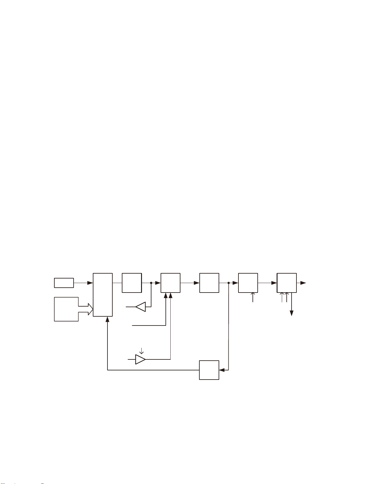
6. Control Circuit
The control circuit consists of the ASIC (IC507) and its
peripheral circuits. IC507 mainly performs the following:
1) Switching between transmission and reception via the
PTT signal input.
2) Reading system, zone, frequency, and program data from
the memory circuit.
3) Sending frequency program data to the PLL.
4) Controlling the squelch on/off using the DC voltage from
the squelch circuit.
5) Controlling the audio mute circuit using the decode data
input.
6-1. ASIC
The ASIC (IC507) is a 32bit RISC processor, equipped
with a peripheral function and ADC/DAC.
This ASIC operates at 18.432MHz clock and 3.3V/1.5V
DC. It controls the fl ash memory, SRAM, DSP, the receive
circuit, the transmitter circuit, the control circuit, and the display circuit and transfers data to or from an external device.
6-2. Memory Circuit
The memory circuit consists of the ASIC (IC507), the
SRAM (IC503) and the flash memory (IC501). The flash
memory has a capacity of 32Mbit which contains the transceiver control program for the ASIC and stores the data. It
also stores the data for the transceiver channels and operating parameters that are written by the FPU. This program
can be easily written from external devices. The SRAM has
a capacity of 1Mbit which contains the work area and data
area.
电路说明
6. 控制电路
控制电路由 ASIC (IC507) 和外围电路组成。IC507 主要执
行以下功能 :
1) 由输入的 PTT 信号切换发射和接收。
2) 从存储电路读取系统、区域、频率和编程数据。
3) 将频率数据发送到 PLL。
4) 由静噪电路的 DC 电压控制静噪的开 / 关。
5) 由输入的解码数据控制音频静音电路。
6-1. ASIC
ASIC (IC507) 是 32 位 RISC 处理器,具备外围功能和
ADC/DAC。
该 ASIC 以 18.432MHz 时钟和 3.3V/1.5V DC 运行。用以控
制闪存、SRAM、DSP、接收电路、发射电路、控制电路以及显
示电路,并与外部设备双向传输数据。
6-2. 存储电路
存储电路由 ASIC (IC507)、SRAM (IC503) 和闪存 (IC501)
组成。闪存具有 32M 位的容量,包含 ASIC 的车载对讲机控制
程序并储存数据。同时还保存车载对讲机信道的数据及 FPU
写入的运行参数。可以轻松通过外部设备写入此程序。SRAM
具有 1M 位的容量,包含工作区和数据区。
Flash memory
■
Note: The flash memory stores the data that is written
by the FPU (KPG-141D(C)), tuning data (Deviation,
Squelch, etc.) and fi rmware program (User mode, Test
mode, Tuning mode, etc.).
SRAM (static memory)
■
Note: The SRAM has a temporary data area and work area.
6-3. Display Unit
The display unit is composed of the LCD driver IC (IC1),
the LCD & Key backlight, etc.
The LCD is controlled using the 4 serial lines (LCDDI,
LCDCE, LCDCL, LCDDO) from the ASIC (IC507).
6-4. Key Detection Circuit
The keys are detected using an LCD driver IC (IC1). If a
pressed key is detected by IC1, the information is passed to
IC507 through the serial line.
■ 闪存
注意 : 闪存可储存 FPU (KPG-141D(C)) 写入的数据、调谐数
据 ( 频偏、静噪等 ) 以及固件程序 ( 用户模式、测试模式、
调谐模式等 )。
■ SRAM ( 静态存储器 )
注意 : SRAM 设有临时数据区和工作区。
6-3. 显示单元
显示单元由 LCD 驱动 IC (IC1)、以及 LCD 和按键背光等部
分组成。
LCD 通过 ASIC (IC507)的4条串行控制线 (LCDDI、
LCDCE、LCDCL、LCDDO) 进行控制。
6-4. 按键检测电路
使用 L CD 驱动 IC ( IC1) 检测按键。如果 IC1 检测到已有
按键按下,则会通过串行线路通知 IC507。
24

NX-820
CIRCUIT DESCRIPTION /
6-5. DSP
The DSP circuit consists of a DSP (IC502) and processes the baseband signal. The DSP operates on an external
clock of 18.432MHz (the same as the IC507), the I/O section
operates at 3.3V and the core section operates at 1.5V. The
DSP carries out the following processes:
• 4 level FSK processing
• Analog FM pre-emphasis/de-emphasis
• Vocoder processing between the audio codec and modulation/demodulation
• CAI processing, such as error correction encoding
• QT/DQT encoding/decoding
• DTMF encoding/decoding
• MSK encoding/decoding
• 2-tone encoding/decoding
• Compressor/expander processing
• Voice scrambler processing
• Transmit/receive audio fi ltering processing
• Microphone amplifi er AGC processing
• Audio mute processing
• Modulation level processing
电路说明
6-5. DSP
DSP 电路由 D S P (IC502) 组成,用以处理基带信号。D SP
在 18.432M H z 的外部时钟上运行 ( 与 I C507 相同 ),I / O 部
分以 3.3V 运行,核心部分以 1.5V 运行。DSP 进行以下处理 :
· 4 级 FSK 处理
· 模拟 FM 预加重 / 去加重
· 音频编解码器和调制 / 解调之间的声码器处理
· CAI 处理,例如纠错编码
· QT/DQT 编码 / 解码
· DTMF 编码 / 解码
· MSK 编码 / 解码
· 2音编码/解码
· 压缩器 / 扩展器处理
· 语音扰频器处理
· 发射 / 接收音频滤波处理
· 麦克风放大器 AGC 处理
· 音频静音处理
· 调制电平处理
7. Power Supply Circuit
+B is connected to the Final amplifier and the DC/DC
converter IC (IC405). IC405 regulates the +B voltage to 5.0V
(50M). 50M operates whenever +B is supplied. IC401 (33M)
and IC408 (15M) are enabled while the 50M is operating.
33M and 15M provide the power to the ASIC (IC507),
DSP (IC502), and Flash memory. At this time the ASIC
starts working. The voltage detector IC (IC402) watches the
+B voltage. If the +B voltage is higher than 8.6V, IC402 (/
BINT) outputs High. If the /BINT signal is high, Q403 (SB
SW) is turned on by the SBC signal from the ASIC. (High :
SBC=ON, Low : SBC=OFF). When the SB is turned on, IC1
(80C), IC404 (50C), Q402 (80ANT), Q404 (80T), Q415, 416
(150C), Q417 (50R) and Q408 (50CS) start working. IC409,
Q409 and Q410 are controlled by the SBC signal. If the
SBC signal becomes High, IC409 (33C) operates, and Q409
(33A_2) and Q410 (50MC SW) turn on.
The ASIC sets the TXC signal to High during transmission to the supply power (80T) for the transmission circuit.
The ASIC sets the signals (RXC) to High during reception to
the supply power (50R) for the reception circuit.
When the ASIC detects the PSW (Power switch) signal,
IGN (Ignition sense) signal or /BINT signal, it sets the SBC
signal to Low, and turns the transceiver power (SB) off.
When D401 and Q401 detect an over-voltage condition, they
turn Q403 (SB SW) off, but the ASIC continues to function.
7. 电源电路
+B 连接至末级放大器和 DC/DC 转换器 IC (IC405)。IC405
将 +B 电压调整至 5.0V (50M )。提供 + B 时,50M 运行。50M
运行时,IC401 (33M) 和 IC408 (15M) 启用。
33M 和 15M 对 ASIC (IC507)、DSP (IC502) 和闪存供电。
此时 ASIC 开始工作。电压检测 IC (IC402) 观测 +B 电压。如
果 +B 电压高于 8.6V,则 IC402 (/BINT) 输出高。如果 /BINT
信号高,则 Q403 (SB SW) 由 ASI C 的 SBC 信号开启。( 高 :
SBC=ON,低 : SBC=OFF)。SB 开启时,IC1 (80C)、IC404 (50C)、
Q402 (80ANT)、Q404 (80T)、Q415、416 (150C)、Q417 (50R)
和 Q408 (50CS) 开始工作。IC409、Q409 和 Q410 由 SBC 信号
控制。如果 S B C 信号变高,I C409 (33C) 运行,并开启 Q409
(33A_2) 和 Q410 (50MC SW)。
发射期间,ASI C 将 T XC 信号控制为高,为发射电路供电
(80T)。接收期间,ASIC 将信号 (R XC ) 控制为高,为接收电
路供电 (50R)。
当 ASIC 检测 PSW ( 电源开关 ) 信号、IGN ( 点火感应 )
信号或 /BINT 信号时,它将SBC 信号控制为低,关闭车载对
讲机电源 (SB)。当 D401 和 Q401 检测到过电压情况时,它们
将关闭 Q403 (SB SW)。但 ASIC 仍然工作。
25
NX-820
㻗㻮
㻲㻠㻜㻝
㻽㻠㻜㻝
㻿㼃
㻵㻯㻠㻜㻞
㻰㻱㼀
㻽㻠㻜㻟
㻿㼃
CIRCUIT DESCRIPTION /
㻵㻯㻠㻜㻡
㻰㻯㻛㻰㻯
㻵㻯㻠㻜㻝
㻭㼂㻾
㻵㻯㻠㻜㻤
㻭㼂㻾
㻵㻯㻠㻜㻢
㻭㼂㻾
㻵㻯㻠㻜㻥
㻭㼂㻾
㻿㻮㻯㻞
㻛㻻㼂㻾㻮
㻳㻼㻿㻯
㻛㻮㻵㻺㼀
㻲㻡㻜㻞
㻿㻮㻯㻞
㻵㻯㻠㻜㻣
㻭㼂㻾
㻽㻠㻝㻜
㻿㼃
电路说明
㻵㻯㻠㻜㻥
㻭㼂㻾
㻿㻮㻯㻞
㻗㻮
㻡㻜㻹
㻟㻟㻹
㻝㻡㻹
㻟㻟㻭
㻟㻟㻭㼋㻞
㻟㻟㻯
㻟㻟㻳㻼㻿
㻡㻜㻹㻯
㻿㻮
㻲㼕㼚㼍㼘㻌㻭㻹㻼
㻲㻺㻯㻌㻮㼁㻲㻲
㻭㻿㻵㻯㻌㻰㼕㼓㼕㼠㼍㼘
㻰㻿㻼㻌㻵㻛㻻㻘㻌㻲㻸㻭㻿㻴
㼂㻯㼀㻯㼄㻻㻘㻌㻿㻾㻭㻹
㻯㼘㼛㼏㼗㻌㻮㼡㼒㼒
㻭㻿㻵㻯㻌㻯㼛㼞㼑
㻰㻿㻼㻌㻯㼛㼞㼑
㻭㻿㻵㻯㻌㻭㼚㼍㼘㼛㼓
㻰㻭㻯㻘㻌㻭㼡㼐㼕㼛
㻼㻸㻸㻌㻵㻯
㼀㻯㼄㻻㻔㻝㻢㻚㻤㻹㻴㼦㻕
㻾㻿㻞㻟㻞㻯㻌㻯㼛㼚㼢㼑㼞㼠㼑㼞
㻰㻙㼟㼡㼎㻌㻝㻡
㻭㼡㼐㼕㼛㻌㻼㼛㼣㼑㼞㻌㻭㻹㻼
㻰㼕㼟㼜㼘㼥㻌㼁㼚㼕㼠
㻰㻙㼟㼡㼎㻌㻝㻡
26
㻤㻜㻯
㻵㻯㻝
㻭㼂㻾
㻰㻰㻯㻸㻷
㻲㻡㻜㻟
㼀㼄㻯
㻰㻿㼃
㻽㻠㻝㻡㻘㻠㻝㻢
㻰㻯㻛㻰㻯
㻽㻠㻜㻠
㻿㼃
㻽㻠㻜㻞
㻿㼃
㻵㻯㻠㻜㻠
㻭㼂㻾
㻿㻭㼂㻱
㻾㼄㻯
Fig. 7 Power supply circuit / 图 7 电源电路
㻽㻠㻜㻤
㻿㼃
㻽㻠㻝㻣
㻿㼃
㻝㻡㻜㻯
㻤㻜㼀
㻤㻜㻭㻺㼀
㻡㻜㻯
㻡㻜㻯㻿
㻡㻜㻾
㼂㻯㻻㻌㼀㼡㼚㼑㻌㻔㻭㼟㼟㼕㼟㼠㻕
㻲㼞㼛㼚㼠㻌㻱㼚㼐㻌㼀㼡㼚㼕㼚㼓
㼀㼄㻌㻰㼞㼕㼢㼑㻘㻌㻭㻼㻯
㻭㻺㼀㻌㻿㼃
㻵㻛㻻㻌㻱㼤㼜㼍㼚㼐㼑㼞
㻼㻸㻸㻌㻵㻯
㻰㼕㼟㼜㼘㼥㻌㼁㼚㼕㼠㻔㻸㻱㻰㻕
㻯㼛㼙㼙㼛㼚㻌㻭㻹㻼
㻲㼋㼕㼚㻌㻭㻹㻼
㻾㻲㻌㻭㻹㻼㻔㼂㻯㻻㻌㻮㼡㼒㼒㻕
㼀㼄㻛㻾㼄㻌㼂㻯㻻
㻸㻺㻭㻘㻌㻹㼕㼤㼑㼞㻘㻌
㻵㻲㻌㻭㻹㻼㻘㻌㻲㻹㻌㻵㻯

NX-820
CIRCUIT DESCRIPTION /
8. Signaling Circuit
8-1. Encode (QT/DQT/DTMF/2-tone/MSK)
Each signaling data signal of the QT, DQT, DTMF, 2-tone
and MSK is generated by the DSP circuit, superposed on a
modulation signal and output from the ASIC (IC507). Each
deviation of the TX QT, DQT, DTMF, 2-tone and MSK tones
are adjusted by changing the output lev el of the DSP (IC502)
and the resulting signal is routed to the VCO and PLL.
8-2. Decode (QT/DQT/DTMF/2-tone/MSK)
The audio signal is removed from the FM detection signal
sent to the DSP circuit and the resulting signal is decoded
by the DSP.
9. Compander Circuit
The term “compander” means compressor and expander.
The compander reduces noise by utilizing a compressor and
an expander. The DSP (IC502) performs this operation. The
Compander can be turned on or off using the FPU.
电路说明
8. 信令电路
8-1. 编码 (QT/DQT/DTMF/2 音 /MSK)
DSP 电路生成 QT、DQT、DTMF、2 音和 MSK 的各信令信号,
这些信号被叠加到调制信号上并从 ASIC (IC507) 输出。T X
QT、DQT、DTMF、2 音和 MSK 音各自的频偏通过改变 DSP (IC502)
的输出电平进行调整,产生的信号被送至 VCO 和 PLL。
8-2. 解码 (QT/DQT/DTMF/2 音 /MSK)
音频信号从发送到 DSP 电路的 FM 检测信号中提取,产生
的信号由 DSP 解码。
9. 压扩器电路
“Compander”一词表示压缩器和扩展器。压扩器利用压缩
器和扩展器减低噪音。DSP (I C502) 用以执行此操作。可用
FPU 开启或关闭压扩器。
27
NX-820
COMPONENTS DESCRIPTION /
Display unit (X54-3830-10)
Ref. No. Part Name Description
IC1 IC LCD driver
Q3 Transistor TX/Busy LED switch
Q6 Transistor TX/Busy LED switch
Q8 Transistor LCD backlight switch
Q9 Transistor Backlight switch
Q10 Transistor Status LED switch
Q11 Transistor Backlight switch
D2 Diode Line protection
D5-9 LED Key backlight
D11-21 LED LCD backlight
D22 LED Status LED
D23 LED TX/Busy LED
D24 LED LCD backlight
D25 Varistor Line protection
D26 Diode Key control
D27 Zener diode Over DC supply protection
元件说明
显示单元 (X54-3830-10)
有关号码 零件名称 说 明
IC1 IC LCD 驱动
Q3 晶体管 LED 开关 (TX/BUSY)
Q6 晶体管 LED 开关 (TX/BUSY)
Q8 晶体管 LCD 背光开关
Q9 晶体管 背光开关
Q10 晶体管 LED 开关 ( 状态 )
Q11 晶体管 背光开关
D2 二极管 线路保护
D5-9 LED 键背光
D11-21 LED LCD 背光
D22 LED 状态 LED
D23 LED TX/BUSY LED
D24 LED LCD 背光
D25 变阻器 线路保护
D26 二极管 键控制
D27 稳压二极管 DC 供电过高保护
TX-RX unit (X57-8240-13)
Ref. No. Part Name Description
IC1 IC AVR (80C)
IC2 IC PLL system
IC3 IC DC AMP (CV/Assist)
IC102 IC TX power module
IC103 IC OP AMP (APC)
IC201 IC DC AMP (BPF)
IC301 IC AND gate
IC303 IC FM system
IC304 IC DC AMP (RSSI)
IC401 IC AVR (33M)
IC402 IC Voltage detector (BINT)
IC404 IC AVR (50C)
IC405 IC DC/DC converter (50M)
IC406 IC AVR (33A)
IC407 IC AVR (33GPS)
IC408 IC AVR (15M)
IC409 IC AVR (33C)
IC501 IC Flash memory
IC502 IC DSP
IC503 IC SRAM
IC504 IC Reset
IC506 IC Buffer AMP (Clock)
收发单元 (X57-8240-13)
有关号码 零件名称 说 明
IC1 IC 稳压器 (80C)
IC2 IC PLL 系统
IC3 IC 直流放大器 (CV/ 辅助 )
IC102 IC 功率模块
IC103 IC OP 放大器 (APC)
IC201 IC 直流放大器 (BPF)
IC301 IC AND 柵
IC303 IC FM 系统
IC304 IC 直流放大器 (RSSI)
IC401 IC 稳压器 (33M)
IC402 IC 电压检测器 (BINT)
IC404 IC 稳压器 (50C)
IC405 IC DC/DC 转换器 (50M)
IC406 IC 稳压器 (33A)
IC407 IC 稳压器 (33GPS)
IC408 IC 稳压器 (15M)
IC409 IC 稳压器 (33C)
IC501 IC 闪存
IC502 IC DSP
IC503 IC SRAM
IC504 IC 复位
IC506 IC 射频缓冲放大器 ( 时钟 )
28

NX-820
COMPONENTS DESCRIPTION /
Ref. No. Part Name Description
IC507 IC ASIC
IC508 IC AND gate
IC509 IC
IC511 IC BUS buffer
IC512 IC Level shift
IC513 IC Dual BUS buffer (FNC3/FNC1)
IC514 IC Dual BUS buffer (FNC2/FNC4)
IC515 IC I/O expander
IC516 IC RS-232C driver
IC701 IC VCO MOD/VREF
IC702 IC LPF (APC/DMO)
IC703 IC MIC SUM AMP/LPF (DI)
IC705 IC BPF/Buffer AMP (SQ)
IC711 IC RX SUM AMP/LPF (RX AF)
IC712 IC D/A converter
IC713 IC MIC/RX selector
IC714 IC AF power AMP
IC716 IC Dual BUS buffer (TXD1/MKEO)
IC801 IC Dual BUS buffer (TXD2/RXD2)
Q1 Transistor DC switch (Assist)
Q2 FET DC switch (Assist)
Q4 Transistor Ripple fi lter
Q5 Transistor Buffer AMP (PLL fi n)
Q6 FET RX VCO
Q7 FET TX VCO
Q8,9 FET T/R VCO switch
Q10,11 Transistor Buffer AMP
Q102 Transistor TX drive AMP
Q105 FET DC switch (H/L power)
Q106 Transistor DC switch (50C)
Q201 FET RX 1st mixer
Q202 Transistor LNA
Q303 Transistor Tripler
Q305 Transistor 1st IF AMP
Q401 Transistor
Q402 Transistor DC switch (80ANT)
Q403 FET DC switch (SB)
Q404 Transistor DC switch (80T)
Q405 Transistor DC switch (80ANT)
Q407 Transistor DC switch (50MC)
Q408 Transistor DC switch (50CS)
Q409 FET DC switch (33A_2)
Q410 Transistor DC switch (50MC)
Dual BUS buffer (HOOK/RXD/MKEYI)
DC switch (Over DC supply
protection)
元件说明
有关号码 零件名称 说 明
IC507 IC ASIC
IC508 IC AND 柵
IC509 IC 双总线缓冲器 (HOOK/RXD/MKEYI)
IC511 IC 总线缓冲器
IC512 IC 电平位移
IC513 IC 双总线缓冲器 (FNC3/FNC1)
IC514 IC 双总线缓冲器 (FNC2/FNC4)
IC515 IC I/O 扩展器
IC516 IC RS-232C 驱动
IC701 IC VCO 调制 /VREF
IC702 IC LPF (APC/DMO)
IC703 IC 麦克风 SUM 放大器 /LPF (DI)
IC705 IC BPF/ 射频缓冲放大器 (SQ)
IC711 IC RX SUM 放大器 /LPF (RX AF)
IC712 IC D/A 转换器
IC713 IC 麦克风 /RX 选择器
IC714 IC AF 功率放大器
IC716 IC 双总线缓冲器 (TXD1/MKEO)
IC801 IC 双总线缓冲器 (TXD2/RXD2)
Q1 晶体管 直流开关 ( 辅助 )
Q2 场效应管 直流开关 ( 辅助 )
Q4 晶体管 纹波滤波器
Q5 晶体管 射频缓冲放大器 (PLL fin)
Q6 场效应管 RX VCO 振荡器
Q7 场效应管 TX VCO 振荡器
Q8,9 场效应管 收发 VCO 直流开关
Q10,11 晶体管 射频缓冲放大器
Q102 晶体管 驱动放大器
Q105 场效应管 直流开关 ( 高 / 低功率 )
Q106 晶体管 直流开关 (50C)
Q201 场效应管 第一混频器
Q202 晶体管 LNA
Q303 晶体管 三倍频器
Q305 晶体管 第一 IF 放大器
Q401 晶体管 直流开关 (DC 供电过高保护 )
Q402 晶体管 直流开关 (80ANT)
Q403 场效应管 直流开关 (SB)
Q404 晶体管 直流开关 (80T)
Q405 晶体管 直流开关 (80ANT)
Q407 晶体管 直流开关 (50MC)
Q408 晶体管 直流开关 (50CS)
Q409 场效应管 直流开关 (33A_2)
Q410 晶体管 直流开关 (50MC)
29
NX-820
COMPONENTS DESCRIPTION /
Ref. No. Part Name Description
Q411 Transistor DC switch (80T)
Q412 Transistor DC switch (80ANT)
Q414 Transistor DC switch (150C)
Q415,416 Transistor DC/DC converter
Q417 Transistor DC switch (50R)
Q418 FET DC switch (SB)
Q501 FET DC switch (System)
Q502 Transistor DC switch (Horn alert)
Q503 FET DC switch (Horn alert)
Q504 Transistor DC switch (IGN)
Q701 FET SQL noise BW switch
Q702 Transistor Noise AMP
Q703,704 Transistor MIC AGC
Q705 FET Mute (MI1)
Q706 FET Mute (MI2)
Q708 Transistor Pop noise prevention switch
Q709 FET AF mute switch
D2 Zener diode Over voltage protection
D4
D5
D6
D7
D8
D9,10
D11
D13
D14 Diode Speed up
D15
D16,17 Diode T/R switch
D101 Zener diode Over voltage protection
D102 Diode Voltage shift
D103 Diode Reverse current prevention
D104,105 Diode TX power detection
D106 Diode Reverse current provention
D107 Diode Antenna switch
D108,109 Diode Over DC supply protection
D110,110 Diode Antenna switch
D112-114 Diode Over DC supply protection
D202-207
Variable capaci-
tance diode
Variable capaci-
tance diode
Variable capaci-
tance diode
Variable capaci-
tance diode
Variable capaci-
tance diode
Variable capaci-
tance diode
Variable capaci-
tance diode
Variable capaci-
tance diode
Variable capaci-
tance diode
Variable capaci-
tance diode
RX VCO frequency control
TX VCO frequency control
PLL f-in BPF tune
RX VCO assist tune
TX VCO assist tune
RX VCO assist tune
TX VCO assist tune
PLL f-in BPF tune
FM modulation
RX BPF tune
元件说明
有关号码 零件名称 说 明
Q411 晶体管 直流开关 (80T)
Q412 晶体管 直流开关 (80ANT)
Q414 晶体管 直流开关 (150C)
Q415,416 晶体管 DC/DC 转换器
Q417 晶体管 直流开关 (50R)
Q418 场效应管 直流开关 (SB)
Q501 场效应管 直流开关 ( 系统 )
Q502 晶体管 直流开关 ( 喇叭提示 )
Q503 场效应管 直流开关 ( 喇叭提示 )
Q504 晶体管 直流开关 (IGN)
Q701 场效应管 静噪噪声开关
Q702 晶体管 噪声放大器
Q703,704 晶体管 麦克风 AGC
Q705 场效应管 静音 (MI1)
Q706 场效应管 静音 (MI2)
Q708 晶体管 噪声预防开关
Q709 场效应管 AF 静音开关
D2 稳压二极管 过电压防护
D4 可变电容二极管 频率控制 /RX VCO
D5 可变电容二极管 频率控制 /TX VCO
D6 可变电容二极管 PLL f-in BPF 调谐
D7 可变电容二极管 RX VCO 辅助调谐
D8 可变电容二极管 TX VCO 辅助调谐
D9,10 可变电容二极管 RX VCO 辅助调谐
D11 可变电容二极管 TX VCO 辅助调谐
D13 可变电容二极管 PLL f-in BPF 调谐
D14 二极管 加速
D15 可变电容二极管 FM 调制器
D16,17 二极管 收发开关
D101 稳压二极管 过电压防护
D102 二极管 电压偏移
D103 二极管 逆向电流保护
D104,105 二极管 功率检测器
D106 二极管 逆向电流保护
D107 二极管 天线开关
D108,109 二极管 DC 供电过高保护
D110,110 二极管 天线开关
D112-114 二极管 DC 供电过高保护
D202-207 可变电容二极管 RX BPF 调谐
30
 Loading...