

Page 1
UHF DIGITAL TRANSCEIVER
NX-800/800H
SERVICE MANUAL
© 2008-4 PRINTED IN JA PAN
B51-8823-00 (N) 446
Cover
(A01-2194-11)
Key top
(K29-9401-03)
CONTENTS
GENERAL .....................................................2
SYSTEM SET-UP .........................................4
REALIGNMENT ...........................................5
INSTALLATION ............................................7
DISASSEMBLY FOR REPAIR ....................14
CIRCUIT DESCRIPTION ............................17
COMPONENTS DESCRIPTION .................23
PARTS LIST ...............................................26
EXPLODED VIEW ......................................39
PACKING ....................................................40
TROUBLE SHOOTING ..............................41
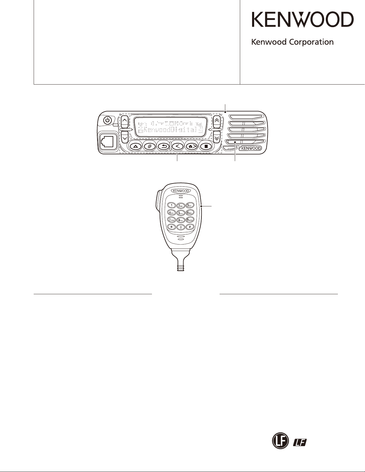
Panel assy
(A62-1162-03)
Microphone
(T91-0639-35)
ADJUSTMENT ..........................................44
TERMINAL FUNCTION .............................62
PC BOARD
DISPLAY UNIT (X54-3640-10) ...............72
TX-RX UNIT (X57-7390-XX) (A/2) ........ 74
TX-RX UNIT (X57-7390-XX) (B/2) ........78
INTERCONNECTION DIAGRAM ..............79
SCHEMATIC DIAGRAM ............................80
BLOCK DIAGRAM .....................................98
LEVEL DIAGRAM ....................................100
SPECIFICATIONS ...................BACK COVER
This product complies with the RoHS directive for the European market.
This product uses Lead Free solder.
Page 2

NX-800/800H
GENERAL
Document Copyrights
Copyright 2008 by Kenwood Corporation. All rights re-
served.
No part of this manual may be reproduced, translated,
distributed, or transmitted in any form or by any means,
electronic, mechanical, photocopying, recording, or otherwise, for any purpose without the prior written permission
of Kenwood.
Disclaimer
While every precaution has been taken in the preparation
of this manual, Kenwood assumes no responsibility for errors or omissions. Neither is any liability assumed for damages resulting from the use of the information contained
herein. Kenwood reserves the right to make changes to any
products herein at any time for improvement purposes.
Firmware Copyrights
The title to and ownership of copyrights for firmware
embedded in Kenwood product memories are reserved for
Kenwood Corporation. Any modifying, reverse engineering, copy, reproducing or disclosing on an Internet website
of the firmware is strictly prohibited without prior written
consent of Kenwood Corporation. Furthermore, any reselling, assigning or transferring of the fi rmware is also strictly
prohibited without embedding the firmware in Kenwood
product memories.
NXDN Transceivers:
The AMBE+2(TM) voice coding technology is embedded
in the fi rmware under the license of Digital Voice Systems,
Inc.
INTRODUCTION
SCOPE OF THIS MANUAL
This manual is intended for use by experienced technicians familiar with similar types of commercial grade communications equipment. It contains all required service
information for the equipment and is current as of this publication date. Changes which may occur after publication
are covered by either Service Bulletins or Manual Revisions,
which are issued as required.
ORDERING REPLACEMENT PARTS
When ordering replacement parts or equipment information, the full part identifi cation number should be included.
This applies to all parts: components, kits, and chassis. If
the part number is not known, include the chassis or kit
number of which it is a part and a suffi cient description of
the required component for proper identifi cation.
PERSONAL SAFETY
The following precautions are recommended for personal
safety :
• DO NOT transmit if someone is within two feet (0.6 meter) of the antenna.
• DO NOT transmit until all RF connectors are secure and
any open connectors are properly terminated.
• SHUT OFF this equipment when near electrical blasting
caps or while in an explosive atmosphere.
• All equipment should be properly grounded before power-up for safe operation.
• This equipment should be serviced by only qualified
technicians.
PRE-INSTALLATION CONSIDERATIONS
1. UNPACKING
Unpack the radio from its shipping container and check
for accessory items. If any item is missing, please contact
KENWOOD immediately.
2. LICENSING REQUIREMENTS
Federal regulations require a station license for each
radio installation (mobile or base) be obtained by the equipment owner. The licensee is responsible for ensuring transmitter power, frequency, and deviation are within the limits
permitted by the station license.
Transmitter adjustments may be performed only by a
licensed technician holding an FCC fi rst, second or general
class commercial radiotelephone operator’s license. There is
no license required to install or operate the radio.
3. PRE-INSTALLATION CHECKOUT
3-1. Introduction
Each radio is adjusted and tested before shipment. How-
ever, it is recommended that receiver and transmitter operation be checked for proper operation before installation.
3-2. Testing
The radio should be tested complete with all cabling and
accessories as they will be connected in the fi nal installation. Transmitter frequency, deviation, and power output
should be checked, as should receiver sensitivity, squelch
operation, and audio output. Signaling equipment operation
should be verifi ed.
4. PLANNING THE INSTALLATION
4-1. General
Inspect the vehicle and determine how and where the
radio antenna and accessories will be mounted.
Plan cable runs for protection against pinching or crush-
ing wiring, and radio installation to prevent overheating.
2
Page 3
GENERAL
NX-800/800H
4-2. Antenna
The favored location for an antenna is in the center of a
large, flat conductive area, usually at the roof center. The
trunk lid is preferred, bond the trunk lid and vehicle chassis
using ground straps to ensure the lid is at chassis ground.
4-3. Radio
The universal mount bracket allows the radio to be
mounted in a variety of ways. Be sure the mounting surface
is adequate to support the radio’s weight. Allow suffi cient
space around the radio for air cooling. Position the radio
close enough to the vehicle operator to permit easy access
to the controls when driving.
4-4. DC Power and wiring
1. This radio may be installed in negative ground electrical
systems only. Reverse polarity will cause the cable fuse
to blow. Check the vehicle ground polarity before instal-
lation to prevent wasted time and effort.
2. Connect the positive power lead directly to the vehicle
battery positive terminal. Connecting the Positive lead
to any other positive voltage source in the vehicle is not
recommended.
3. Connect the ground lead directly to the battery negative
terminal.
4. The cable provided with the radio is suffi cient to handle
the maximum radio current demand. If the cable must be
extended, be sure the additional wire is suffi cient for the
current to be carried and length of the added lead.
SERVICE
This radio is designed for easy servicing. Refer to the
schematic diagrams, printed circuit board views, and alignment procedures contained in this manual.
NOTE
• If you do not intend to use the speaker 3.5-mm jack and
the D-sub 25-pin connector, fi t the supplied speaker-jack
cap and D-sub cap to stop dust and sand from getting in.
• If the transceiver is turned ON or OFF when the power-
on/off status message is enabled, the transceiver sends
the status.
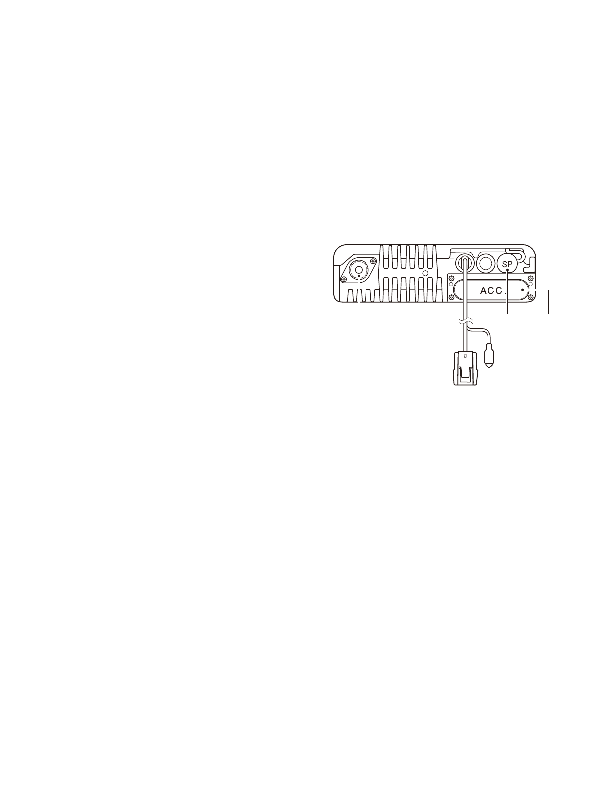
Antenna
connector
Speaker
jack cap
Ignition
sense cable
Power input
connector
D-sub
cap
5. INSTALLATION PLANNING – CONTROL STATIONS
5-1. Antenna system
Control station. The antenna system selection depends
on many factors and is beyond the scope of this manual.
Your KENWOOD dealer can help you select an antenna system that will best serve your particular needs.
5-2. Radio location
Select a convenient location for your control station radio which is as close as practical to the antenna cable entry
point. Secondly, use your system’s power supply (which
supplies the voltage and current required for your system).
Make sure suffi cient air can fl ow around the radio and power supply to allow adequate cooling.
3
Page 4
NX-800/800H
SYSTEM SET-UP
Merchandise received
License and frequency allocated by FCC
Choose the type of transceiver
Are you using
the remote kit?
NO
Are you using
the ignition sense cable?
NO
Transceiver programming
Are you using
the public address?
NO
Are you using
the voice guide & storage
unit?
NO
Frequency range RF power Type
450.0~520.0MHz 30W K
450.0~520.0MHz
YES
YES
See page 5.
A personal computer (IBM PC or compatible), programming
interface (KPG-46/46A), and programming software (KPG-111D)
are required for programming.
YES
YES
KRK-10
KCT-46
KAP-2
VGS-1
45W
(490~512MHz: 40W
512~520MHz: 35W)
See page 9.
(Option)
See page 7.
(Option)
See page 8.
(Option)
See page 10.
(Option)
HK
Are you using
the external speaker?
NO
Are you using
the keypad microphone?
NO
Supplied microphone
Delivery
YES
YES
KES-3, KES-5 or KES-6 External speaker
(Option)
KMC-32 or KMC-36
(Option)
Desk top microphone KMC-9C
4
Page 5
REALIGNMENT
NX-800/800H
1. Modes
User mode
Panel test mode
PC mode
Firmware
programming mode
Clone mode
Firmware version information
Mode Function
User mode For normal use.
Panel test mode
Panel tuning mode
PC mode
Data programming
mode
PC test mode
PC tuning mode
Firmware
programming mode
Clone mode
Firmware version
information
Used by the dealer to check the fundamental characteristics.
Used by the dealer to tune the audio.
Used for communication between the radio
and PC.
Used to read and write frequency data and
other features to and from the radio.
Used to check the radio using the PC.
This feature is included in the FPU.
Used to tune the radio using the PC.
This feature is included in the FPU.
Used when changing the main program of
the fl ash memory.
Used to transfer programming data from
one radio to another.
Used to confi rm the internal fi rmware version.
Panel tuning mode
Data programming mode
PC test mode
PC tuning mode
5. PC Mode
5-1. Preface
The transceiver is programmed by using a personal computer, programming interface (KPG-46/46A) and programming software (KPG-111D).
The programming software can be used with a PC or
compatible. Figure 1 shows the setup of a PC for programming.
PC
KPG-111D
PC
D-SUB
(25-pin)
KPG-46
Transceiver
PC
D-SUB
(9-pin)
KPG-46A
Transceiver
Fig. 1
5-2. Connection procedure
1. Connect the transceiver to the computer using the inter-
face cable and USB adapter (When the interface cable is
KPG-46A, the KCT-53U can be used.).
KPG-46 or KPG-46A or
KPG-46A + KCT-46 +
Tuning cable
(E30-3383-05)
PC
USB
KCT-53U
KPG-46A
Transceiver
2. How to Enter Each Mode
Mode Operation
User mode Power ON
Panel test mode [
PC mode Received commands from PC
Panel tuning mode [Panel test mode] + [
Firmware programming mode [
Clone mode [
Firmware version information [
] + Power ON
]
] + Power ON
] + Power ON
] + Power ON
3. Panel Test Mode
Setting method refer to ADJUSTMENT.
4. Panel Tuning Mode
Setting method refer to ADJUSTMENT.
Notes:
• You must install the KCT-53U driver in the computer to
use the USB adapter (KCT-53U).
• When using the USB adapter (KCT-53U) for the fi rst time,
plug the KCT-53U into a USB port on the computer with
the computer power ON.
2. When the POWER switch on, user mode can be entered
immediately. When PC sends command the transceiver
enter PC mode, and “PROGRAM” is displayed on the
LCD.
When data transmitting from transceiver, the red LED is
lights.
When data receiving to transceiver, the green LED is
lights.
Note:
The data stored in the computer must match the “Model
Name” when it is written into the fl ash memory.
5
Page 6

NX-800/800H
REALIGNMENT
5-3. KPG-46/KPG-46A description
(PC programming interface cable: Option)
The KPG-46/46A is required to interface the transceiver
to the computer. It has a circuit in its D-sub connector
(KPG-46: 25-pin, KPG-46A: 9-pin) case that converts the RS232C logic level to the TTL level.
The KPG-46/46A connects the 8-pin microphone connector of the transceiver to the RS-232C serial port of the computer.
5-4. KCT-53U description (USB adapter: Option)
The KCT-53U is a cable which connects the KPG-46A to
a USB port on a computer.
When using the KCT-53U, install the supplied CD-ROM
(with driver software) in the computer. The KCT-53U driver
runs under Windows 2000 or XP.
5-5. Programming software KPG-111D description
The KPG-111D is the programming software for the
transceiver supplied on a CD-ROM. This software runs under MS-Windows 2000, XP or Vista on an IBM-PC or compatible machine.
The data can be input to or read from the transceiver and
edited on the screen. The programmed or edited data can
be printed out. It is also possible to tune the transceiver.
6. Firmware Programming Mode
6-1. Preface
Flash memory is mounted on the transceiver. This allows the transceiver to be upgraded when new features
are released in the future. (For details on how to obtain the
fi rmware, contact Customer Service.)
6-2. Connection procedure
Connect the transceiver to the personal computer (IBM
PC or compatible) using the interface cable (KPG-46/46A)
and USB adapter (KCT-53U: when the interface cable is
KPG-46A, the KCT-53U can be used.). (Connection is the
same as in the PC Mode.)
Note:
You can only program firmware from the 8-pin microphone connector on the front panel. Using the 25-pin logic
interface on the rear panel will not work.
6-3. Programming
1. Start up the fi rmware programming software (Fpro.exe
(ver. 4.0 or later)). The Fpro.exe exists in the KPG-111D
installed holder.
2. Set the communications speed (normally, 115200 bps)
and communications port in the confi guration item.
3. Set the fi rmware to be updated by File name item.
4. Turn the transceiver power ON with the [
down. Then, the orange LED on the transceiver lights
and “PROGRAM 115200” is displayed.
5. Check the connection between the transceiver and the
personal computer, and make sure that the transceiver is
in the Program mode.
] key held
6. Press write button in the window. When the transceiver
starts to receive data, the [LOADING] display lights.
7. If writing ends successfully, the checksum is calculated
and a result is displayed.
8. If you want to continue programming other transceivers,
repeat steps 4 to 7.
Note:
This mode cannot be entered if the Firmware Program-
ming mode is set to Disable in the Programming software.
6-4. Function
1. If you press the [ ] key while “PROGRAM 115200” is
displayed, the display changes to “PROGRAM 19200”
(The LED blinks green) to indicate that the write speed
is low speed (19200 bps). If you press the [
while “PROGRAM 19200” is displayed, the display
changes to “PROGRAM 38400” (The LED lights red and
orange alternatively). If you press the [
“PROGRAM 38400” is displayed, the display changes
to “PROGRAM 57600” (The LED blinks orange). If you
press the [
played, the display returns to “PROGRAM 115200” (The
LED lights orange).
2. If you press the [
displayed, the checksum is calculated, and a result is displayed. If you press the [
sum is displayed, “PROGRAM 115200” is redisplayed.
] key again while “PROGRAM 57600” is dis-
] key while “PROGRAM 115200” is
] key again while the check-
] key again
] key again while
Note:
Normally, write in the high-speed mode.
7. Clone Mode
Programming data can be transferred from one radio to
another by connecting them via their 8-pin microphone connectors. The operation is as follows (the transmit radio is
the master and the receive radio is a slave).
The following data cannot be cloned.
• Tuning data
• Embedded message with password
• ESN (Electronic Serial Number) data
Notes:
The following data can be cloned.
• Fleet (own)/ID (own) for FleetSync
• Unit ID (own) for NXDN
1. Turn the master transceiver power ON with the [
held down. If the read authorization password is set to
the transceiver, the transceiver displays “CLONE LOCK”
If the password is not set, the transceiver displays
“CLONE MODE”.
2. When you enter the correct password, and “CLONE
MODE” is displayed, the transceiver can be used as the
cloning master. The following describes how to enter
the password.
] key
6
Page 7
REALIGNMENT
NX-800/800H
3.
•
How to enter the password with the microphone keypad;
If you press a key while “CLONE LOCK” is displayed,
the number that was pressed is displayed on the transceiver. Each press of the key shifts the display in order
to the left. When you enter the password and press
the [
] key, “CLONE MODE” is displayed if the entered password is correct. If the password is incorrect,
“CLONE LOCK” is redisplayed.
• How to enter the password with the [
If the [
is displayed, number (0 to 9) are displayd fl ashing. When
you press the [
is determined. If you press the [
the password in this procedure, “CLONE MODE” is
displayed if the entered password is correct. If the password is incorrect, “CLONE LOCK” is redisplayed.
4. Power on the slave transceiver.
5. Connect the cloning cable (Part No. E30-3382-05) to the
modular microphone jacks on the master and slave.
6. Press the [
plays “CLONE MODE” The data of the master is sent to
the slave. While the slave is receiving the data, “PROGRAM” is displayed. When cloning of data is completed,
the master displays “END”, and the slave automatically
] and [ ] keys is pressed while “CLONE LOCK”
] key, the currently selected number
] key on the master while the master dis-
] and [ ] keys;
] key after enterning
operates in the User mode. The slave can then be operated by the same program as the master.
7. The other slave can be continuously cloned. When the
[
] key on the master is pressed while the master displays “END”, the master displays “CLONE MODE”.
Carry out the operation in step 4 to 6. Can not be cloned
if the overwrite password is programmed to the slave.
Note:
Only the same models can be cloned together.
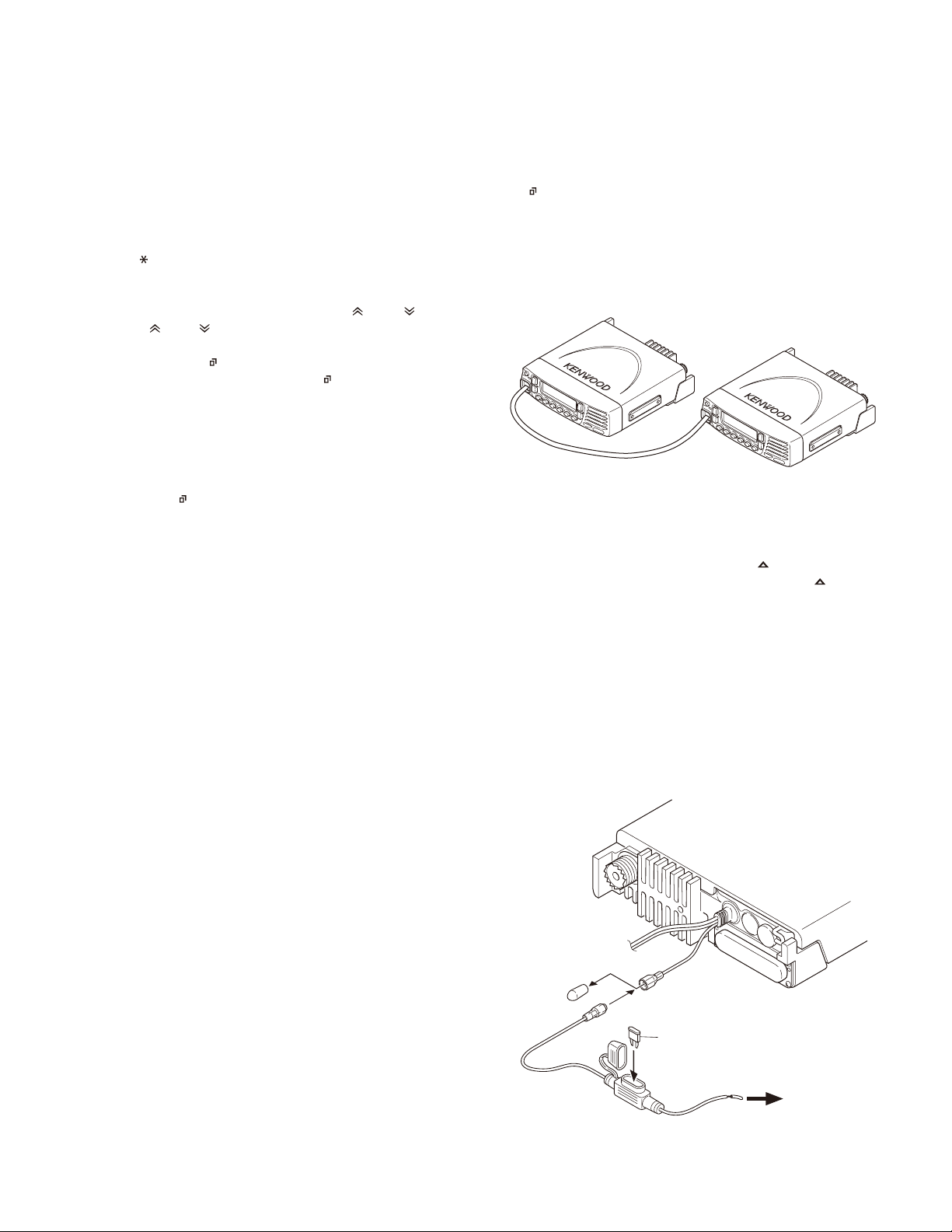
Cloning cable
(E30-3382-05)
Fig. 2
8. Firmware Version Information
Turn the transceiver ON with the [ ] key held down.
Then, the version is displayed during holding the [
] key.
INSTALLATION
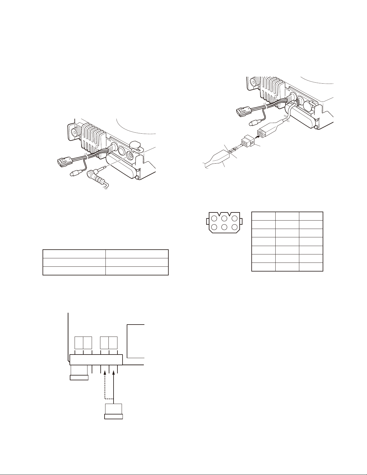
1. Ignition Sense Cable (KCT-46: Option)
The KCT-46 is an optional cable for enabling the ignition
function. The ignition function lets you turn the power to
the transceiver on and off with the car ignition key.
1-1.
Connecting the KCT-46 cable to the transceiver
1. Open the KCT-46 fuse holder and insert a mini blade fuse
(3A). ( q )
2. While holding a clear protective cover, remove the black
cap at the end of the yellow cable (ignition sense cable)
of the transceiver. (
3. Connect the plug of the KCT-46 to the yellow cable ter-
minal of the transceiver. (
4. Connect the other end of the KCT-46 to the ignition line
of the car. (
Note: You must setup using the KPG-111D.
r
)
w
)
)
e
@
.
:
F52-0019-05
Fig. 1
;
Ignition line
of the car
7
Page 8
NX-800/800H
INSTALLATION
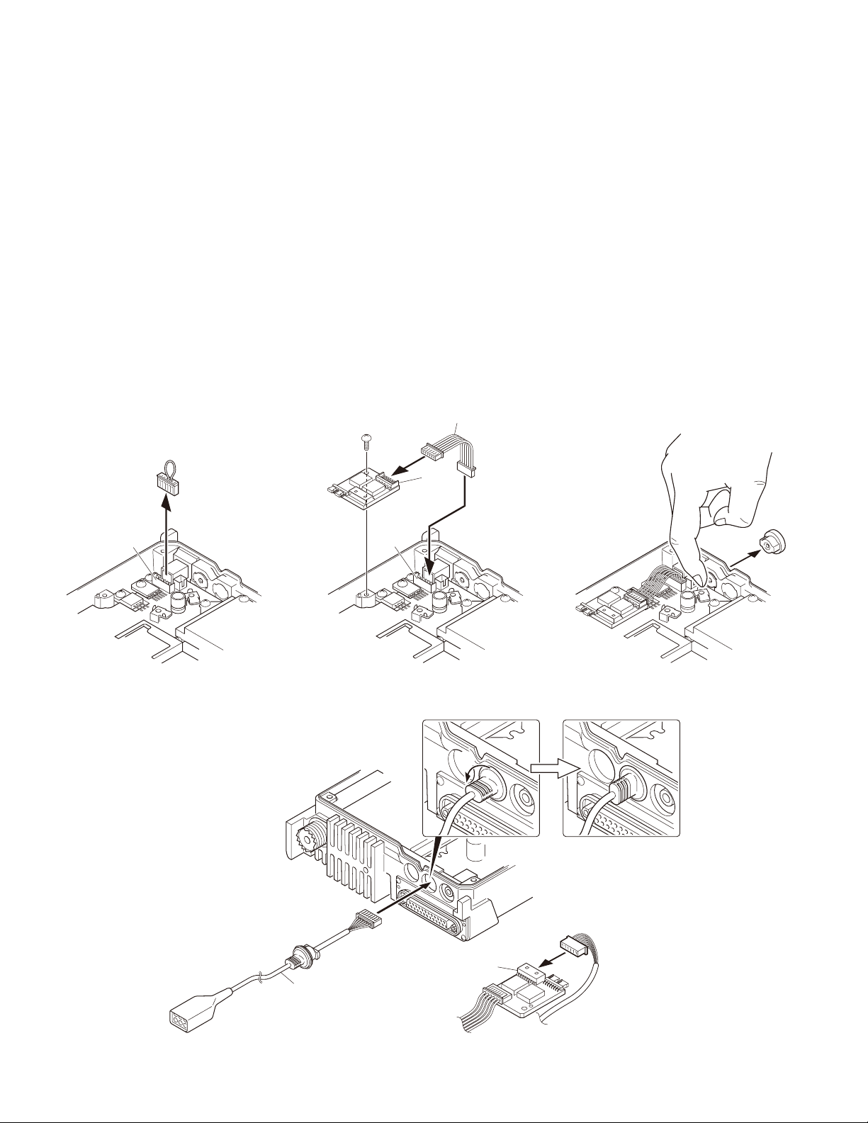
2. Horn Alert/P.A. Relay Unit (KAP-2: Option)
The Horn alert (max. 2A drive), Public address and External speaker function are enabled by installing the KAP-2 in
the transceiver.
2-1. Installing the KAP-2 unit in the transceiver
(The kit A is not used in the KAP-2 accessories)
1. Remove the cabinet, top packing and shielding plate of
the transceiver.
2. Set the KAP-2 relay unit jumper pins according to the
purpose of use.
3. Remove the 6-pin jumper connector inserted in the TX-
RX unit (A/2) connector (CN705). (
4. Insert one side of the lead wire with connector
(E37-1114-05) into the relay unit connector (CN3) (
and the other side into the TX-RX unit (A/2) connector
(CN705) (
e
).
:
CN705
q
)
)
w
@
CN705
5. Place the relay unit at the position shown in Figure 2-2
and secure it to the chassis with a screw.
6. Remove the cap on the rear of the chassis by pushing it
from the inside with your fi nger. (
7. Pass the 6-pin connector of the cable (E37-1113-15)
through the chassis hole (
the chassis hole.
8. Rotate the bush of the cable 90 degrees counterclockwise as viewed from the rear of the chassis. (
9. Insert the 6-pin connector of the cable into the connector
(CN2) of the KAP-2 relay unit. (
Note: You must setup using the KPG-111D.
E37-1114-05
CN3
t
)
r
) and insert the bush into
y
)
u
.
;
)
FIg. 2-1 FIg. 2-2 FIg. 2-3
B
=
CN2
E37-1113-15
>
FIg. 2-4
8
Page 9
INSTALLATION
3.
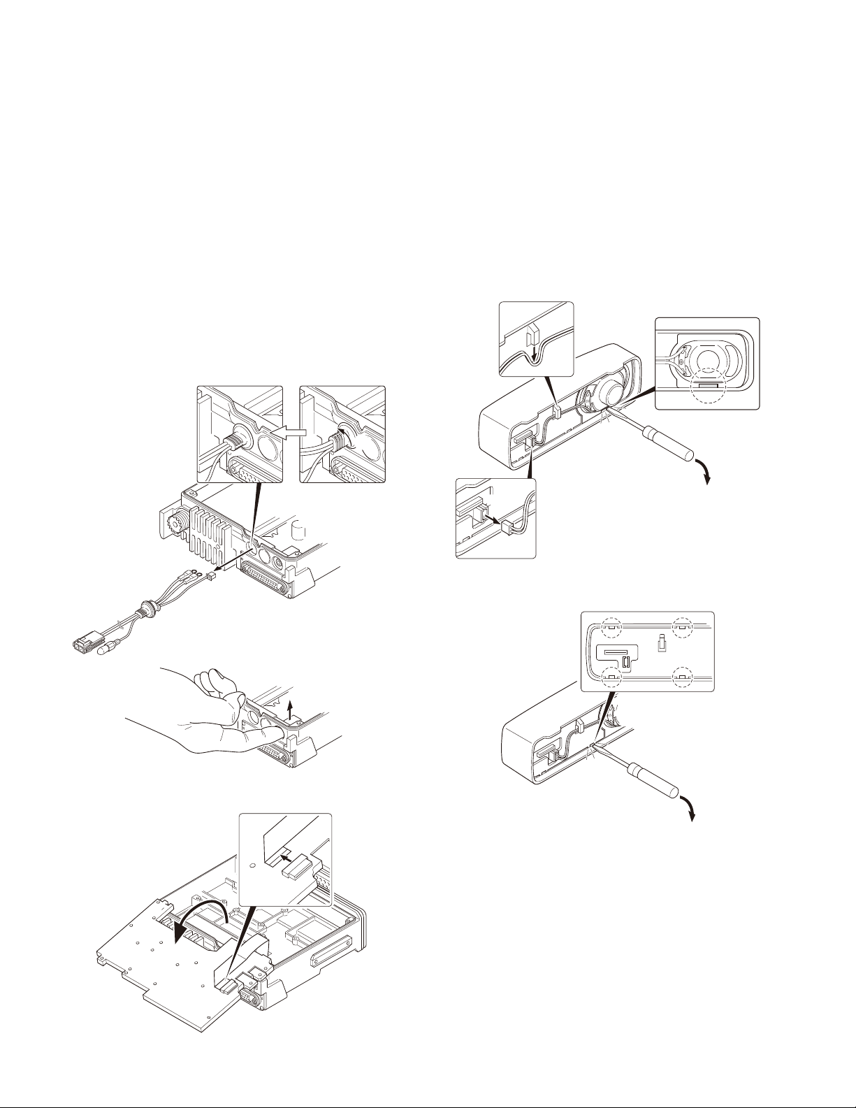
Control Head Remote Kit (KRK-10: Option)
The KRK-10 remote kit is used to remotely operate the
transceiver.
3-1. Installing the KRK-10 kit to the transceiver
1. Remove the front panel from the transceiver.
2. Install the KRK-10 main panel onto the transceiver.
3. Install the KRK-10 rear panel onto the front panel.
4. Connect the KRK-10 main panel to the rear panel with
the cable.
Remove the front panel from the transceiver
■
1. Lift the two tabs of the panel on the bottom of the transceiver with a fl at-head screwdriver (
panel from the chassis (
Note: Confi rm that the tabs of the speaker hardware fi x-
ture and holder is securely fi tted in the front panel.
2. Remove the fl at cable from the connector (CN901) of the
display unit of the panel. (
3. Fold the black line of the flat cable (in three parts) as
shown in Figure 3-2. ( r, t, y )
CN901
w
).
e
)
) and remove the
q
NX-800/800H
Install the KRK-10 main panel onto the transceiver
■
4. Insert the fl at cable that was removed in step 2 above
into the connector (CN1) of the interface unit (A/2) of the
KRK-10 main panel (A62-1101-11). (
Note: The terminal side of the fl at cable must face down
when inserting the fl at cable into the connector.
5. Fit the main panel with four tabs onto the front of the
chassis. (
Note: When installing the main panel onto the front of
the chassis, hold down the fl at cable with your fi ngers to
prevent it from being caught.
i
)
2
)
u
KRK-10 main panel
CN1
>
Chassis
side
B
;
=
;
.
@
Fig. 3-1
=
B
:
Fig. 3-3
Install the KRK-10 rear panel onto the front panel
■
6. Insert the fl at cable attached to the interface unit (A/2) of
the KRK-10 rear panel (A82-0056-21) into the connector
(CN901) of the display unit of the panel (
cable has been pre-inserted in the connector (CN2) of
the rear panel at the time of shipping.)
Note: The terminal side of the fl at cable must face down
when inserting the fl at cable into the connector.
7. Fit the four tabs of the rear panel into the front panel. (
CN901
). (The fl at
o
!0
8
CN2
KRK-10 rear panel
)
Panel
side
Fig. 3-2
Fig. 3-4
9
Page 10
NX-800/800H
CN4
INSTALLATION
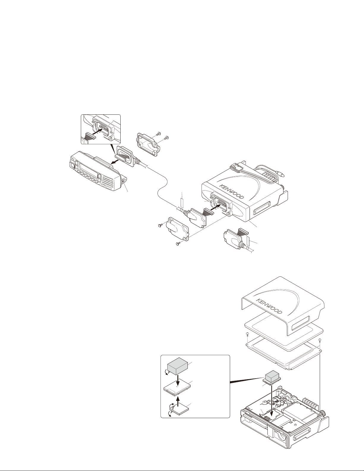
Connect the KRK-10 main panel to the rear
■
panel with the cable
8. Insert one 14-pin connector of the cable (E30-7514-15)
into the connector (CN3) of the interface unit (A/2) of the
main panel. (
Note: Insert the connector that has a sticker onto the
cable to the connector of the main panel.
9. Secure the cable bush on the main panel and fi t the waterproof packing (orange) (
!1
)
) securely over top.
!2
KRK-10
rear panel
10. Install the molded cover (
main panel and secure it with two screws (
11. Insert the other 14-pin connector of the cable into the
connector (CN4) of the interface unit (B/2) of the rear
panel. (
12. Secure the cable bush on the rear panel and fi t the waterproof packing (orange) (
13. Install the molded cover (
rear panel and secure it with two screws (
Note: A cable can be connected from the left side as shown
in the Figure 3-5 or from right side.
However, the 14-pin connector must be connected to correct direction.
Sticker
CN3
!5
)
) over the connector on the
!3
).
!4
) securely over top.
!6
) over the connector on the
!7
).
!8
4. Voice Guide & Storage Unit
(VGS-1: Option)
4-1. Installing the VGS-1 unit in the transceiver
1. Remove the cabinet, top packing and shielding plate of
the transceiver.
2. Attach two cushions to VGS-1 as shown in Figure 4. (
Note: Be sure not to cover the connector with the bot-
tom cushion.
3. Insert the VGS-1 connector (CN1) into the TX-RX unit (A/2)
connector (CN595). (
Note: You must setup using the KPG-111D.
w
)
q
:
Fig. 3-5
)
Cushion
(G13-1994-04)
20 x 30 x 12 mm
VGS-1
(Right side)
KRK-10
main panel
Sticker
CN1
@
10
Cushion
(G13-1992-04)
21 x 21 x 2.5 mm
CN595
Fig. 4
Page 11
INSTALLATION
5. External Speaker (Option)
5-1. KES-3
The KES-3 is an external speaker for the 3.5-mm-diameter
speaker jack.
Connection Procedure
■
1. Connect the KES-3 to the 3.5-mm-diameter speaker jack
on the rear of the transceiver.
NX-800/800H
Connection Procedure
■
Insert the crimp terminal into the Square plug supplied
with the KAP-2.
Fig. 5-1
5-2. KES-5 or KES-6
External speaker KES-5 or KES-6 can be installed for
KAP-2. If KES-5 or KES-6 is installed, it can be set by changing the CN1 short pin from pins 4 and 5 to pins 5 and 6 on
the KAP-2.
KAP-2 CN1 Connect Set Up
4-5 INT. SP or KES-3
5-6 KES-5 or KES-6
When you use the KES-5 or KES-6, plug the short pin to
pins 5 and 6 on the KAP-2.
When you use the INT. SP or KES-3, plug the short pin to
pins 4 and 5 on the KAP-2.
Black/White
lead
4
5
Black lead
Insulating cover
(F29-0481-15)
Square plug
(E59-0419-05)
Fig. 5-3
KAP-2 Cable (E37-1113-15) 6-pin Connector
■
21
3
654
Pin No.
1 Red HR2
2 Blue GND
3 Yellow OSP
4 Green ESP
5 Brown GND
6 Black HR1
Color Name
KAP-2 unit
HR1
INT. SP
KES-3
INT
HR2
CN116
or
EXT
KES-5
or
KES-6
Short pin
Fig. 5-2
11
Page 12
NX-800/800H
INSTALLATION
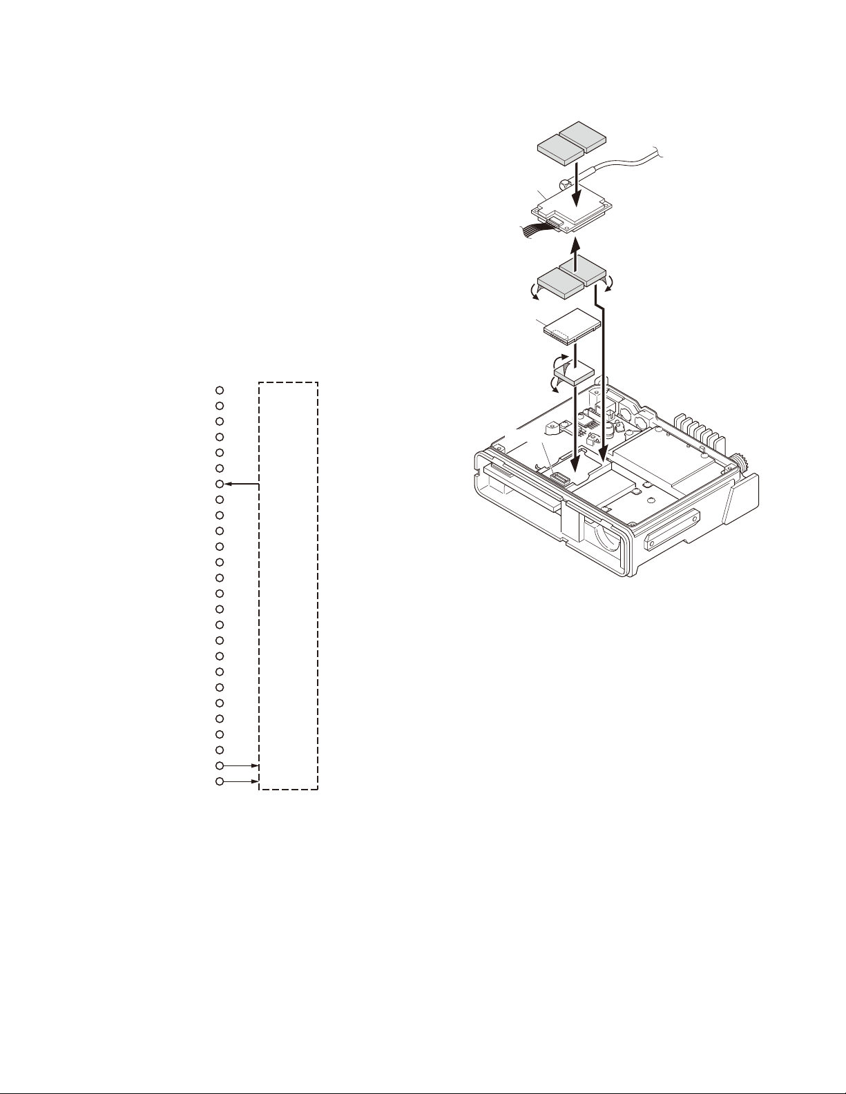
6. GPS Receiver Connection
6-1. Installing the GPS receiver
1. Remove the cabinet, top packing and shielding plate of
the transceiver.
2. Remove the front panel from the transceiver.
3. Attach two cushions to the top of the GPS receiver.
4. Attach the GPS receiver to the shield case with two
cushions as shown in Figure 6-2.
5. Solder each lead of the GPS receiver to a necessary location of each landing on the component side of the TX-RX
unit (A/2).
6. Place the GPS antenna cable in the hollow at the rear of
the chassis. (Fig. 6-2 q )
Note: If the GPS receiver is installed, cut the base of the
convex tab of the top packing with a pair of nippers, or
similar tool. (Fig. 6-3 w )
If the convex tab of the top packing is cut off, the water
proofi ng property is no longer guaranteed.
Note: You must setup using the KPG-111D.
TX-RX unit (A/2)
Solder land
OPT10
OPT11
AGND
26P_RD
26P_TD
TXD2
RXD2
OPT1
OPT3
OPT4
OPT5
5V_1
DTI
OPT8
TXO
OPT7
OPT2
OPT9
RXEO
TXI
RXEI
OPT6
POW
33V
5V_2
DGND
GPS receiver
3M Double coated cushion
No. 4016 (or No. 4416)
30 x 25 mm
GPS receiver
3M Double coated cushion
No. 4016 (or No. 4416)
30 x 25 mm
@
:
Fig. 6-2
Fig. 6-3
12
Fig. 6-1
Page 13
INSTALLATION
Installing the GPS receiver together with the VGS-1
6-2.
1. Remove the cabinet, top packing and shielding plate of
the transceiver.
2. Remove the front panel from the transceiver.
3. Attach a cushion to the bottom of the VGS-1 as shown in
Figure 6-5.
Note: Be sure not to cover the connector with the cush-
ion.
4. Insert the VGS-1 connector (CN1) into the TX-RX unit (A/2)
connector (CN595).
5. Perform step 3 to 6 of “6-1. Installing the GPS receiver”
described on page 13.
Note: You must setup using the KPG-111D.
TX-RX unit (A/2)
Solder land
OPT10
OPT11
AGND
26P_RD
26P_TD
TXD2
RXD2
OPT1
OPT3
OPT4
OPT5
5V_1
DTI
OPT8
TXO
OPT7
OPT2
OPT9
RXEO
TXI
RXEI
OPT6
POW
33V
5V_2
DGND
GPS receiver
NX-800/800H
GPS receiver
VGS-1
CN1
CN595
Fig. 6-5
Fig. 6-4
13
Page 14
NX-800/800H
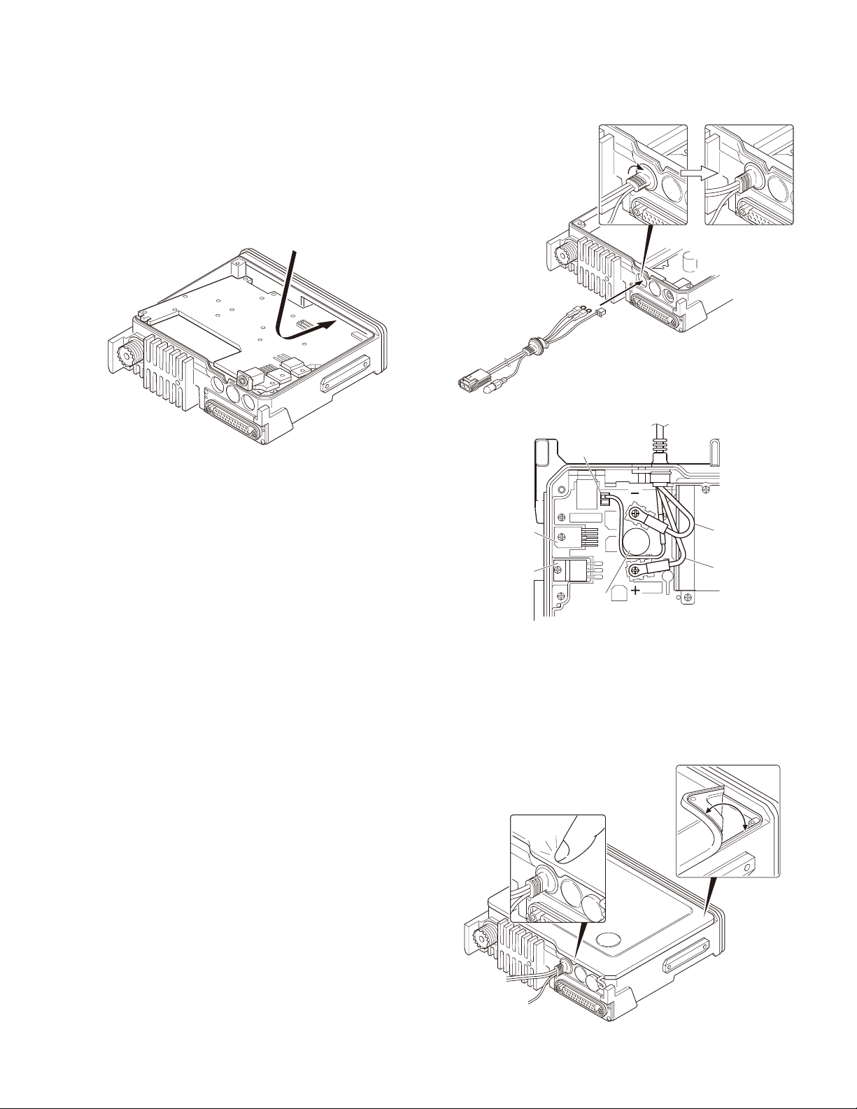
DISASSEMBLY FOR REPAIR
1. Precautions on Disassembly
TX-RX PCB (TX-RX unit A/2) Disassembly
■
1. Remove all screws and antenna terminals on the TX-RX
PCB.
2. Rotate the bush of the power supply cable 90 degrees
counterclockwise as viewed from the rear of the chassis
(
) and remove the power supply cable from the chas-
q
sis (
).
w
3. When the speaker phone jack is pushed up, using your
fi nger, from the rear of the chassis (
is removed from the chassis.
Note: The TX-RX PCB and D-sub PCB (TX-RX unit B/2)
are connected with a fl at cable. Remove them carefully.
4. Turn the TX-RX PCB over and remove the fl at cable from
the connector (CN600). (
5. Remove the TX-RX PCB from the chassis.
r
)
), the TX-RX PCB
e
Removing the speaker hardware fi xture
■
(J21-8481-03) and holder (J19-5485-12)
1. Remove the speaker lead from the holder hook. (
2. Remove the speaker connector from the display unit
connector (CN902). (
3. When removing the speaker hardware fixture, insert a
fl at-head screwdriver at the position shown in Figure 2-1
and tilt it in the direction shown by the arrow. (
4. To remove the holder, insert a fl at-head screwdriver into
tab of the holder and tilt it in the direction shown by the
arrow. (
r
)
w
)
e
q
)
)
:
@
Fig. 1-1
Fig. 1-2
;
:
.
CN902
@
Fig. 2-1
.
;
Fig. 2-2
14
CN600
Fig. 1-3
Page 15
DISASSEMBLY FOR REPAIR
2. Precautions on Reassembly
TX-RX PCB (TX-RX unit A/2) Reassembly
■
1. With the TX-RX PCB turned over, insert the flat cable
from the D-sub PCB (TX-RX unit B/2) into the connector
(CN600) on the TX-RX PCB.
2. Place the TX-RX PCB at its original position, tilt the TX-RX
PCB and install the chassis as shown in Figure 3.
NX-800/800H
@
:
Fig. 4-1
Fig. 3
FINAL shield case (F10-2489-13) installation
■
procedure
1. Place the shield case on the fi nal section of the TX-RX
unit (A/2).
2. The shield case is installed on the positioning boss of
the chassis by pushing down on “PUSH2” (on the shield
case) while pushing “PUSH1” (stamped on two parts on
the shield case) to the right.
Power supply cable installation procedure
■
1. Pass the power supply cable through the chassis hole (
as shown in Figure 4-1 and insert the bush into the chassis hole.
2. Rotate the bush of the power supply cable 90 degrees
clockwise as viewed from the rear of the chassis. (
3. Align the ignition sense connector (yellow) of the power
supply cable around the chemical capacitor (C401) and
connect it to the TX-RX unit (A/2) connector (CN403).
4. Align the + (positive) terminal of the power supply cable
(red) as shown in Figure 4-2 and fi x it to the terminal strip
with a screw.
5. Align the – (negative) terminal of the power supply cable
(black) as shown in Figure 4-2 and fi x it to the terminal
strip with a screw.
w
q
)
CN403
IC715
IC403
C401
Black
Red
Fig. 4-2
)
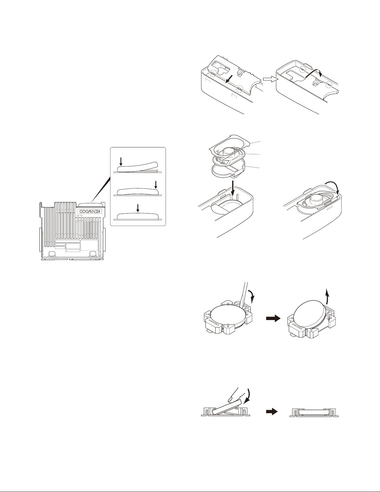
Top packing installation procedure
■
1. Place the top packing over the shielding plate.
2. Fit the convex tab of the top packing into the hollow of
the chassis. (
3. Fit the chassis into the groove of the top packing. (
Verify that the top packing is in close contact with the
chassis.
q
)
)
w
@
:
Fig. 5
15
Page 16
NX-800/800H
DISASSEMBLY FOR REPAIR
D-sub cap installation procedure
■
To improve water resistance, fi t the D-sub cap into the
D-sub terminal hardware fi xture of the transceiver in the following order:
:
@
1. Fit the left side (
fi xture.
2. Fit the right side (
fi xture.
3. Fit the center (
fi xture.
Verify that the D-sub cap is in close contact with the
hardware fi xture.
) of the D-sub cap into the hardware
q
) of the D-sub cap into the hardware
w
) of the D-sub cap into the hardware
e
:
@
.
Fig. 6
Installing the holder (J19-5485-12) and speaker
■
hardware
1. Insert two tabs of the holder (J19-5485-12) into the hol-
lows in the top of the panel. (
2. Push the two tabs of the holder in on the opposite side
of those in step 1 above and fi t them into the hollow in
the bottom of the panel. (
Note: Push in the holder until it snaps in place.
3. Install the speaker holder onto the panel. (
Note: To improve water resistance, fi t the panel into the
groove of the holder.
4. Place the speaker into the speaker holder.
Note: The speaker must not ride on the holder rib.
5. Place the spacer on the speaker.
6. Insert the hardware fi xture (J21-8481-03) into the hollow
of the panel as shown in Figure 7-3, then push two parts
of the hardware fi xture and fi t it into the hollow of the
top of the panel. (Fig. 7-3 r )
Note: Push in the hardware fi xture until it snaps in place.
7. Insert the speaker connector into the display unit con-
nector (CN902).
8. Place the speaker lead on the holder hook.
fi xture (J21-8481-03)
)
q
)
w
e
)
Fig. 7-1
Spacer
Speaker
Speaker holder
.
Fig. 7-2 Fig. 7-3
Removing the lithium cell (W09-0971-05)
■
Insert a screwdriver to groove of one side of the socket
(CN405) and pry the lithium cell up from the socket.
Fig. 8
Installing the lithium cell (W09-0971-05)
■
Insert a lithium cell into one side of the socket (CN405).
Push the lithium cell to insert the lithium cell into the
socket.
Fig. 9
;
16
Page 17
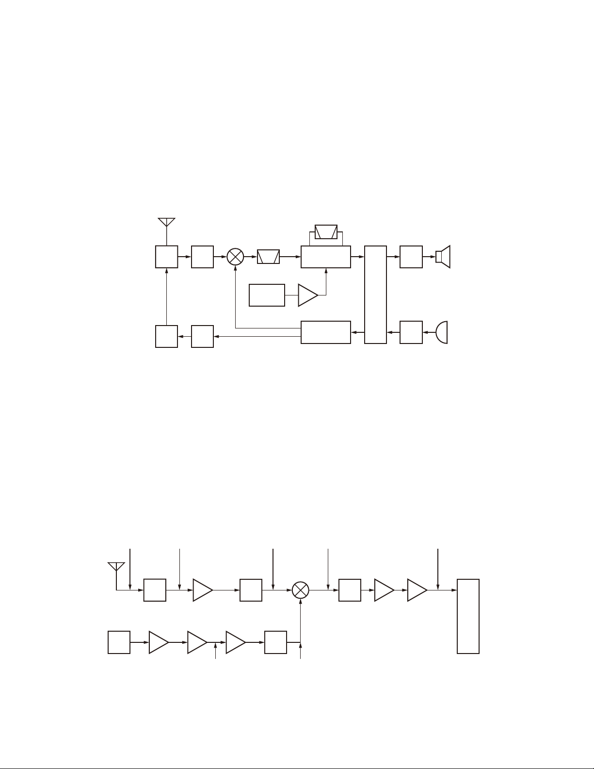
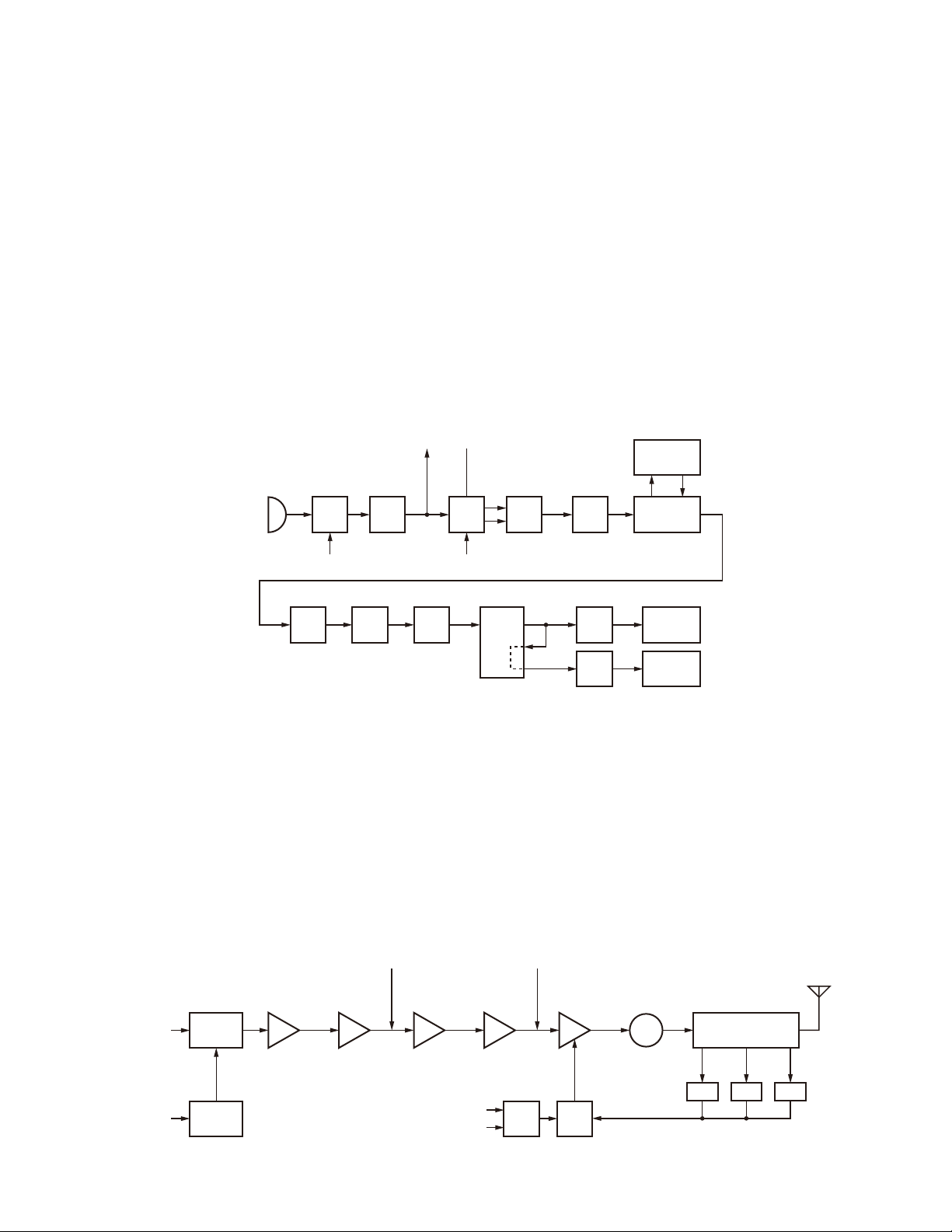
CIRCUIT DESCRIPTION
NX-800/800H
1. Overview
NX-800/800H is a UHF Mobile transceiver designed to
operate in the frequency range of 450 to 520MHz. The unit
consists of receiver, transmitter, phase-locked loop (PLL)
frequency synthesizer, base band parts, power supply, and
control circuits.
ANT
TX/RX: 450~520MHz
ANT
SW
PA
AMPTXAMP
RF
AMP
1st MIX
Fig. 1 Frequency confi guration
MCF
58.05MHz
19.2MHz
VCTCXO
391.95~
461.95MHz
450~520MHz
2. Frequency Confi guration
The receiver is a double-conversion super heterodyne
using first intermediate frequency (IF) of 58.05MHz and
second IF of 450kHz. Incoming signals from the antenna
are mixed with the local signal from the PLL circuit to produce the first IF of 58.05MHz. This is then mixed with
the 57.6MHz second local oscillator output to produce the
450kHz second IF. The transmit signal frequency is generated by the PLL VCO, and modulated by the signal from the
DSP. It is then amplifi ed and fed to the antenna.
CF
450kHz
SP
MIX
IF AMP
x3
57.6MHz
PLL
VCO
AF
AMP
Base band Circuit
MIC
AMP
MIC
3. Receiver System
3-1. RF circuit
The front-end circuit consists of former BPF (D212,
D213), RF amplifier Q210, and latter BPF (D207, D208,
D209 and D210).
The BPF covers frequency ranges 450 to 520MHz.
The latter BPF (D207, D208, D209 and D210) attenuates
the unwanted signals, and sends only the necessary signal
to the fi rst mixer.
–118dBm
ANT
RX
VCO
–120.5dBm –104dBm–114.5dBm –112.5dBm
D212,D213
BPF
Buff AMP
Q9
RF AMP
Q210
Buff AMP
Q10
D207~
D210
BPF
Buff AMP
Q208
1st MIX DBM
BPF
3-2. First Mixer
The signal from the BPF is heterodyned with the fi rst local oscillator signal from the PLL frequency synthesizer circuit at the fi rst mixer DBM (IC204) to become a 58.05MHz
fi rst intermediate frequency (IF) signal.
The fi rst IF signal is fed through a monolithic crystal fi lter
(XF202) to further remove spurious signals.
IC204
0dBm0dBm
XF202
IF AMP
MCF
Q205
IF AMP
Q204
FM SYSTEM IC
IC202
Fig. 2
17
Page 18
NX-800/800H
CIRCUIT DESCRIPTION
3-3. IF circuit
The fi rst IF signal is passed through a four-pole monolithic crystal fi lter (XF202) to reject adjacent channel signal.
The fi ltered fi rst IF signal is amplifi ed by the fi rst IF amplifi er
(Q204, Q205) and then applied to the lF system IC (IC202).
The IF system IC provides a second mixer, AGC amplifi er,
and RSSI (Received Signal Strength Indicator).
The second mixer mixes the first IF signal with the
57.6MHz of second local oscillator output and produces the
second IF signal of 450kHz.
ANT
RF Circuit (Front end)
TCXO
19.2MHz
IC711
(2/2)
IC510
DSP
IC701 IC707IC704
SW
AMT
X1
VC
IC712
Fig. 3
The second IF signal is passed through the ceramic fi lter
(CF201, CF202) to reject the adjacent channel signal. The
fi ltered second IF signal is amplifi ed by AGC amplifi er.
The signal from AGC amplifi er is input to AD converter
(IC510) through ceramic fi lter (CF203) and operational amplifi er (IC201 and IC704).
IC201
INT. SP
EXT. SP
2nd OSC
Q203
x3
VOL
INAMT
IC202
MIX. AGC
BPF
CF201
CF202
MUTE
SW
SW
Q709IC502
CF203
BPF
IC715Q710
AF AMP
3-4. Audio amplifi er circuit
Audio processing (high-pass filter, low-pass filter, deemphasized and so on) at FM mode and decoding at NXDN
mode are processed by DSP. Audio signal from IC510,
IC502 goes through the amplifi er (IC701). The signal then
goes through mute switch (IC707), amplifier (IC711), and
electronic volume control (IC712).
While busy, INAMT becomes High, turn switch (Q709)
on and Mute switch (Q710) off, and signal is fed to AF Power Amp (IC715). While Non-busy, INAMT is become Low,
turn switch (Q709) off and Mute switch (Q710) on, then
there is not AF output.
IC705 (2/2)
FMDET
IC202 IC510
BPF
18
Q702
AMP
3-5. Squelch Circuit
It amplifies the demodulated noise signal from IC202
after fi ltering through BPF circuit. Then, the amplifi ed signal
is converted to DC signal by the detection circuit. The converted signal is fed back to IC510.
D703
RECT
IC705 (1/2)
AMP
IC203 (1/2)
AMP
IC203 (2/2)
AMP
ASQDET
VAGC
RSSI
Fig. 4
Page 19
CIRCUIT DESCRIPTION
NX-800/800H
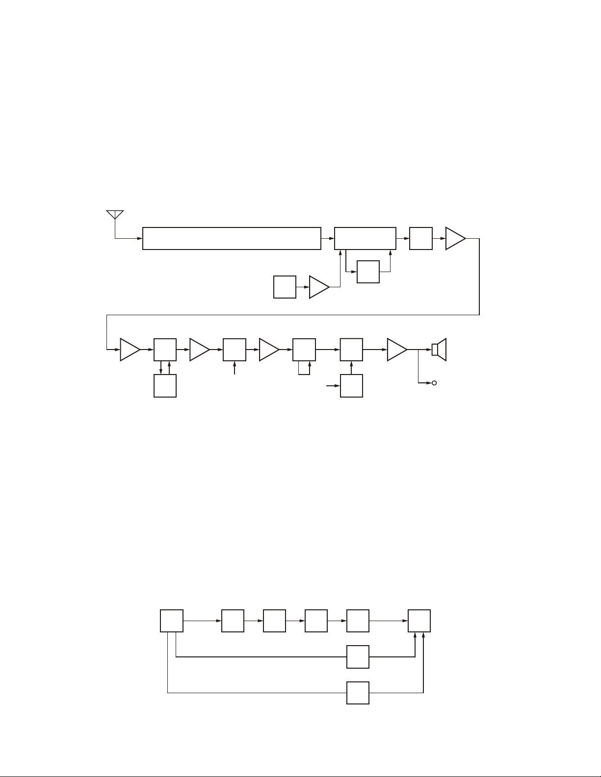
4. Transmitter System
4-1. Audio Band Circuit
The signal from the microphone goes through the mute
switch (Q706), the Mic-Mute signal (MM) becomes Low,
then mute switch (Q706) is turned off. The signal from
microphone goes through Mic-AGC (Q704, Q705, D704,
D705), and goes through switch IC (IC708), and amplifi ed by
Mic-Amp IC706 (1/2), LPF IC706 (2/2) works as anti-aliasing
fi lter.
If an optional scrambler board is installed, the switch
(IC708) adjusts the signal path so that the audio signal is input to the scrambler board.
Optional Scrambler Board
D703,D704
Q705,Q706
INT. MIC
Q707 IC708
SW
MM
AGC
SCSW
SW
4-2. Base Band Circuit
The audio signal output from the base band circuit is
converted to digital data of a sampling frequency of 48kHz.
This digital data is sent to the DSP (IC502), and voice signals
of 300Hz or lower and frequencies of 3kHz or higher are
cut off and an audio range 300Hz to 3kHz is extracted. The
audio signal is then pre-emphasized in FM mode and synthesized with the signals, such as QT and DQT, as required,
and is then output from the IC510. In Digital mode, the audio signal is converted to the 4-Level FSK base band signal
and output from the IC510. The DTMF and MSK base band
signals are also generated by the DSP and output by the
IC510.
LPF (IC702) works as smoothing fi lter. The DAC (IC712)
assigns the base band signal to the VCO and VCTCXO (X1).
At this time, the level output according to the transmit carrier is fi ne-adjusted according to each modulation method.
IC502
IC706
(1/2)
AMP
IC706
(1/2)
LPF
DSP
IC510
LPF
IC702
(2/2)
LPF
IC702
(1/2)
AMP IC712
IC709
(1/2)
4-3. Drive and Final amplifi er
The transmit signal obtained from the TX VCO buffer
amplifi er Q9, is amplifi ed to approximately +17dBm by the
driver amplifi ers Q10, Q101 and Q102.
This amplified signal is passed to the power amplifier
module (power module) IC102, which consists of a MOSFET amplifi er and capable of transmission output power.
4-4. APC circuit
The Automatic transmission power control (APC) circuit
stabilizers the transmitter output power at a predetermined
0dBm +17dBm
Drive AMP
Q10
Drive AMP
Q101
MOD
MB
Buff AMP
Q9
TX VCO
VCTCXO
19.2MHz
Fig. 5
IC1
AMP
AMP
IC5 (2/2)
X1
VCTCXO
VCO
level by detecting the power module output with a diodes
D108, D109 and D110. Diodes D108, D109 and D110 apply
a voltage to DC amplifi er IC103 (1/2).
IC103 (2/2) compares the APC control voltage (PC) generated by microprocessor IC510 and DC amplifi er IC101 (1/2,
2/2) with the detection output voltage from IC103 (1/2) to
control the Vgg Pin of IC102, and stabilizes transmission output.
The APC circuit is confi gured to protect over-current of
the power module due to fluctuations of the load at the
antenna end and to stabilize transmission output at voltage
and temperature variations.
*D103: NX-800H only
Drive AMP
Q102
PC
MP
Final AMP
IC102
Gate
bias
DC
AMP
IC101 IC103
DC
AMP
D103*,D104,
D106,D216
SW ANT Filter
D108
D109
DET
DET
D110
DET
ANT
Fig. 6
19
Page 20
NX-800/800H
CIRCUIT DESCRIPTION
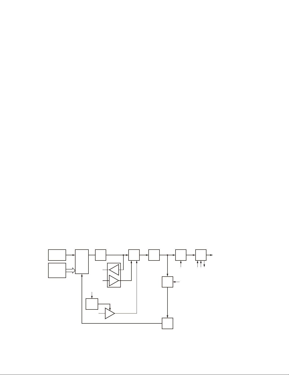
5. PLL Frequency Synthesizer
5-1. VCTCXO (X1)
VCTCXO (X1) generates a reference frequency of 19.2
MHz for the PLL frequency synthesizer. This reference
frequency is applied to pin 9 of the PLL IC (IC3) and connected to IF circuit as a 2nd local signal through Tripler. The
VCTCXO oscillation frequency is determined by DC voltage
of VC terminal. The VC voltage is fi xed to 1.65V by R1 and
R2, and supplied to VC terminal through IC2. Modulation
signal is also fed to VC terminal through IC2.
The frequency adjustment is achieved by switching the
ratio of dividing frequency that is not adjusted by the DC
voltage impressed to VC. The resolution of adjusting frequency is approximately 4Hz.
5-2. VCO
There is a RX VCO and a TX VCO.
The TX VCO (Q6) generates a transmit carrier and the RX
VCO (Q5) generates a 1st local signal. For the VCO oscillation frequency, the transmit carrier is 450 to 520MHz and
the 1st local signal is 391.95 to 461.95MHz.
The VCO oscillation frequency is determined by one system of operation switching terminal “T/R” and two systems
of voltage control terminals “C/V” and “V-assist”.
The operation switching terminal, “T/R”, is controlled by
the control line (/T_R) output from the MCU (IC510). When
the /T_R logic is low, the VCO outputs the transmit carrier
and when it is high, it outputs a 1st local receive signal.
The voltage control terminals, “CV” and “V-assist”, are
controlled by the PLL IC (IC3) and MCU (IC510) and the
output frequency changes continuously according to the
applied voltage. For the modulation input terminal, “VCO
MOD”, the output frequency changes according to the applied voltage. This is used to modulate the VCO output.
“VCO MOD” works only when “/T_R” is low.
5-3. PLL IC (IC3)
PLL IC compares the differences in phases of the VCO
oscillation frequency and the VCTCXO reference frequency,
returns the difference to the VCO CV terminal and realizes
the “Phase Locked Loop” for the return control. This allows
the VCO oscillation frequency to accurately match (lock) the
desired frequency.
When the frequency is controlled by the PLL, the frequency convergence time increases as the frequency difference increases when the set frequency is changed. To
supplement this, the MCU is used before control by the PLL
IC to bring the VCO oscillation frequency close to the desired frequency. As a result, the VCO CV voltage does not
change and is always stable at approx. 3.0V.
The desired frequency is set for the PLL IC by the MCU
(IC510) through the 3-line “SDO1”, “SCK1”, “PCS_RF” serial bus. Whether the PLL IC is locked or not is monitored
by the MCU through the “PLD” signal line. If the VCO is
not the desired frequency (unlock), the “PLD” logic is low.
5-4. Local Switch (D101, D205)
The connection destination of the signal output from
the buffer amplifi er (Q10) is changed with the diode switch
(D101) that is controlled by the transmission power supply,
80T, and the diode switch (D205) that is controlled by the
receive power supply, 50R. If the 80T logic is high, it is connected to a send-side pre-drive (Q101). If the 80T logic is
low, it is connected to a local amplifi er (Q208).
20
X1
19.2MHz
VC
TCXO
SDO1
SCK1
/PCS RF
Q5,Q6
D3,D4
IC4
D7~D12,D14
VCO
IC5
BUFF
AMP
IC3 Q9
PLL
Loop
Filter
CV
VCO MOD
150C
Q1
Ripple
Filter
ASSIST
Fig. 7
BUFF
AMP
LPF
Q3
Q10
BUFF
AMP
50C
50C
D101,D205
T/R
SW
80T
50R
to Local Amplifier
to TX stage
Page 21

CIRCUIT DESCRIPTION
NX-800/800H
6. Control Circuit
The control circuit consists of MCU (IC510) and its pe-
ripheral circuits. IC510 mainly performs the following;
1) Switching between transmission and reception by PTT
signal input.
2) Reading system, zone, frequency, and program data
from the memory circuit.
3) Sending frequency program data to the PLL.
4) Controlling squelch on/off by the DC voltage from the
squelch circuit.
5) Controlling the audio mute circuit by decode data input.
6-1. MCU
The MCU (IC510) is 32bit RISC processor, equipped with
peripheral function and ADC/DAC.
This MCU operates at 18.432MHz clock and 3.3V /1.5V
DC. Controls the flash memory, SRAM, DSP, the receive
circuit, the transmitter circuit, the control circuit, and the display circuit and transfers data to or from an external device.
6-2. Memory Circuit
Memory circuit consists of the MCU (IC510) and the
SRAM (IC503), the fl ash memory (IC501). The fl ash memory has capacity of 32Mbit that contains the transceiver control program for the MCU and stores the data. It also stores
the data for transceiver channels and operating parameter
that are written by the FPU. This program can be easily
written from external devices. The SRAM has capacity of
1Mbit that contains work area and data area.
Flash memory
■
Note: The fl ash memory stores the data that is written
by the FPU (KPG-111D), tuning data (Deviation, Squelch,
etc.), and fi rmware program.
SRAM (static memory)
■
Note: The SRAM has temporary data area and work
area.
When the power supply is off, it is backed up by an inter-
nal secondary lithium battery. Therefore, the save data does
not break.
Real-time clock
■
The clock function is based on real-time clock IC (IC504).
When the power supply is off, it is backed up by an internal
secondary lithium battery
6-3. Display Unit
The display unit is composed of the MCU (IC911) and
the memory IC (IC913), and the LCD & Key backlight etc.
The LCD Ass’y (with LCD Driver) is controlled using the
bus lines on the connector (CN905) of the display unit. It
corrects the LCD contrast voltage using IC909.
6-4. Key Detection Circuit
Keys are detected using Key scan circuit in IC911. The
/KI* and KO* signals that are normally pulled up go low
when any key is pressed.
6-5. DSP
The DSP circuit consists of a DSP (IC502) and processes
the base band signal. The DSP operates on an external
clock of 18.432MHz (the same as the IC510), the I/O section operates at 3.3V and the core section operates at 1.5V.
The DSP carries out the following processes:
• 4Level FSK processing
• Analog FM pre-emphasis/de-emphasis
• Vocoder processing between audio codec and modula-
tion/demodulation
• CAI processing, such as error correction encoding
• QT/DQT encoding/decoding
• DTMF encoding/decoding
• MSK encoding/decoding
• 2TONE encoding/decoding
• Compressor/expander processing
• Voice scrambler processing
• Transmit/receive audio fi ltering processing
• Microphone amplifi er AGC processing
• Audio mute processing
• Modulation level processing
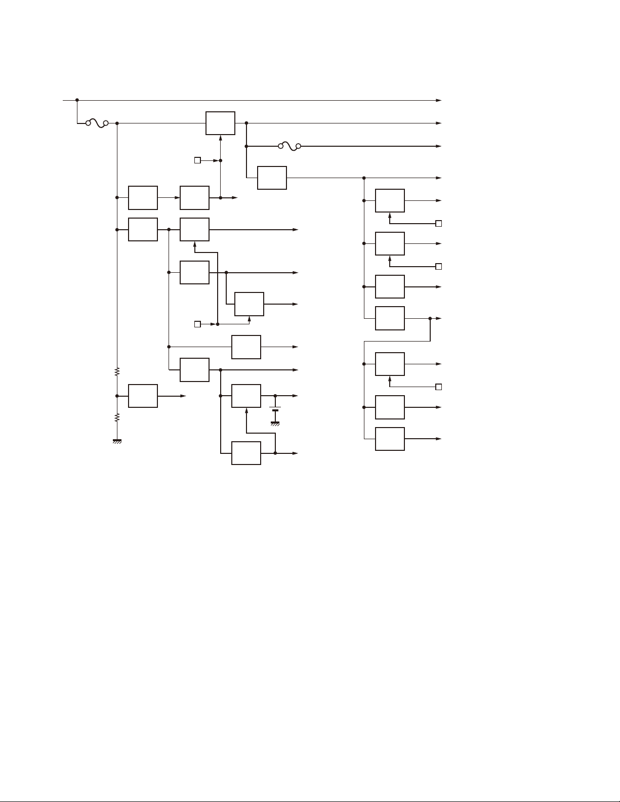
7. Power Supply Circuit
+B is connected to Final amplifi er and DC/DC converter
IC (IC405). IC405 regulates +B voltage to 5.0V (50M). 50M
operates whenever +B is supplied. IC402 (33M), IC408 (33A)
and IC409 (15M) are enabled while the 50M are operating.
33M and 15M provide the power to MCU, DSP, and
Flash memory. At this time MCU starts working. Voltage
detector IC (IC401) watches +B voltage. If +B voltage is
higher than 8.6V, IC401 (/BINT) outputs High. If the /BINT
signal is high, Q404 (SB SW) is turned on by SBC signal
from MCU. (High: SB=ON, Low: SB=OFF). When the SB
is turned on, IC403 (80C), IC404 (50C), IC406 (33C), IC407
(33GPS) and IC410 (150C) start working. Q416 and Q412
are controlled by SBC signal. If the SBC signal becomes
High, Q416 (33A-2) operates and Q412 (50MC SW) are
turned on.
The MCU controls the TXC signal to High during transmission to supply power (80T) for transmission circuit. The
MCU controls the signals (RXC) to High during reception to
supply power (80R, 50R) for reception circuit.
When the MCU detects the PSW (Power switch) signal,
IGN (Ignition sense) signal or /BINT signal, it controls the
SBC signal to Low, and turns the transceiver power (SB) off.
When D401 and Q401 detect over-voltage condition, they
turns Q404 (SB SW) off. But the MCU still works.
If +B is not provided to the transceiver, the power is provided to SRAM and RTC through the secondary battery connected with CN405.
21
Page 22
NX-800/800H
CIRCUIT DESCRIPTION
+B
F401
5A
D401
DET
IC405
DC/DC
IC401
DET
SBC
Q401
INV
Q412
50MC SW
IC408
AVR
SBC
IC402
AVR
/BINT
Q404
SB SW
IC403
/OVRB
Q416
SW
IC409
AVR
Q411
33BU SW
AVR
50MC
33A
33A-2
15M
33M
33BU
F501
2A
RS-232C Driver
ASIC (Analog)
Audio circuit
ASIC, DSP core
ASIC, DSP I/O
Flash memory
SRAM, RTC
CN405
Q407
80T SW
Q408
80R SW
IC410
DC/DC
IC404
AVR
Q409
50R SW
IC406
AVR
+B
SB
SB
80C
80T
80R
150C
50C
50R
33C
Final Amp
Audio Amp, Display Block
PA connector
D_Sub 25Pin connector
Internal Option
Display Block
TX circuit
TXC
RX circuit
RXC
Assist, Tune circuit
VCO, Internal Option,
I/O expander, FM IC
RX circuit
RXC
TCXO, PLL
IC506
DET
8. Signaling Circuit
8-1. Encode (QT/DQT/DTMF/MSK/2TONE)
Each signaling data signal of QT, DQT, DTMF and MSK is
generated by the DSP circuit, superposed on a modulation
signal and output from IC510. The modulation balance of
the QT/DQT signal is adjusted by the D/A converter (IC712)
and the resulting signal is routed to the modulation input of
the VCO and VCTCXO (X1). The each deviation of the TX
QT, DQT, DTMF and MSK tone is adjusted by changing the
output level of the IC510 and the resulting signal is routed
to VCO and VCXO. The RX DTMF tone is routed to the receive audio signal system, and is output from the speaker.
8-2. Decode (QT/DQT/DTMF/2TONE/MSK)
The audio signal is removed from the FM detection
signal sent to the DSP circuit and the resulting signal is decoded.
33GPS
IC407
AVR
MCU Reset
Internal Option
Fig. 8
9. Compander Circuit
The term “compander” means compressor and expander. The compander reduces noise by utilizing a compressor
and an expander. The NX-800/800H contains DSP (IC502) to
perform this operation. The NX-800/800H compander can
be turned on or off using the FPU.
22
Page 23
NX-800/800H
COMPONENTS DESCRIPTION
Display unit (X54-3640-10)
Ref. No. Part Name Description
IC901 MOS-IC AFO/BLC SW
IC902 MOS-IC AF Buffer AMP (AFO)
IC903 MOS-IC Voltage Regulator (5C)
IC904 MOS-IC Voltage Regulator (33C)
IC905 MOS-IC Bus Buffer (TXD0)
IC906 MOS-IC DC/DC Converter (N100C)
IC907 MOS-IC Dual Bus Buffer (RXD0/RXD1)
IC908 MOS-IC AND Gate (TXD1/RXD0)
IC909 MOS-IC Buffer AMP (LCD Contrast ADJ)
IC910 MOS-IC Bus Buffer (D0-D7)
IC911 MOS IC MCU
IC912 MOS-IC Bus Buffer (A1-A2)
IC913 ROM IC Flash ROM
Q901 FET AFO SW
Q902 Transistor HK/RXD0 SW
Q904 Transistor HK/RXD0 SW
Q905 Transistor TX/RX LED (TX)
Q906 Transistor TX/RX LED (BUSY)
Q908 Transistor LCD Back Light SW
Q909 Transistor DIMER SW (LCD Back Light)
Q910 Transistor LCD BACK LIGHT SW
Q911 FET Dimer SW (LCD Back Light)
Q913 FET LCD Reset SW
D901 Varistor Surge Absorption (DM/KVL)
D902 Varistor Surge Absorption (HK/RXD)
D903 Zener Diode Over DC Supply Protection
D904 Varistor Surge Absorption (BLC/AFO)
D906 Varistor LINE protection (SB)
D907 Zener Diode OVER DC Supply Protection
D908 Diode KEY Matrix
D910 Diode
D911,912 Diode KEY Matrix
D913 Diode Line Protection (PTT/TXDO)
D914 LED TX/RX LED
D915~926
D927~936
D937 Diode Level Shift (PRST)
LED LCD Back Light
LED KEY Back Light
Reverse Current Prevention (HK/
RXD)
TX-RX unit (X57-7390-XX)
Ref. No. Part Name Description
IC1 MOS-IC Temp Sensor
IC2 MOS-IC Buffer AMP (TCXO modulation)
IC3 MOS-IC PLL IC
IC4 MOS-IC Buffer AMP (VCO tune)
IC5 MOS-IC VCO Modulation/Buffer AMP (CV)
IC101 MOS-IC Auto Power Control
IC102 MOS-IC Final AMP (RF Power Module)
IC103 MOS-IC Auto Power Control
IC201 MOS-IC Buffer AMP (2nd IF DET)
IC202 Analogue IC IF IC
IC203 MOS-IC Buffer AMP (RSSI/VAGC)
IC204 MOS-IC 1st Mixer
IC205,206
IC401 MOS-IC Voltage Detector (BINT)
IC402 MOS-IC Voltage Regulator (33M)
IC403 MOS-IC Voltage Regulator (80C)
IC404 MOS-IC Voltage Regulator (50C)
IC405 Analogue IC DC/DC Converter (50M)
IC406 BI-POLAR IC Voltage Regulator (33C)
IC407 MOS-IC Voltage Regulator (33GPS)
IC408 MOS-IC Voltage Regulator (33A)
IC409 MOS-IC Voltage Regulator (15M)
IC410 Analogue IC DC/DC Converter (150C)
IC501 ROM IC Flash ROM
IC502 MCU DSP (BGA)
IC503 SRAM IC SRAM (BGA)
IC504 MOS-IC RTC
IC505 MOS-IC Delay
IC506 MOS-IC Reset (MCU)
IC507 MOS-IC Bus Buffer (BFSX2)
IC508 MOS-IC Buffer AMP (18.432MHz)
IC509 MOS-IC Bus Buffer (BER CLK/BER DATA)
IC510 MOS-IC MCU (BGA)
IC511 MOS-IC AND (PCS_RF/HD2)
IC512 MOS-IC Level Shift (AND ITXD1/SCTXD)
IC513 MOS-IC Buffer AMP (TXD2)
IC514 MOS-IC Level Shift (I2CCK/I2CDT)
IC515 MOS-IC Level Shift (TXDO/RTSO)
IC516 MOS-IC Level Shift (RXDO/CTSO)
IC517 MOS-IC I/O Expander
MOS-IC Buffer AMP (BPF tune)
23
Page 24

NX-800/800H
COMPONENTS DESCRIPTION
Ref. No. Part Name Description
IC518 MOS-IC RS-232C Driver
IC701 MOS-IC LPF (RXAF)
IC702 MOS-IC LPF (MOD)
IC703 MOS-IC LPF (APC/DEO)
IC704 MOS-IC Buffer AMP (2nd IF DET)
IC705 MOS-IC BRF/Buffer AMP (SQ)
IC706 MOS-IC LPF/SUM AMP
IC707 MOS-IC RXAF/RXEI SW
IC708 MOS-IC AF SW (TXO/TXI)
IC709 MOS-IC
IC710 MOS-IC AF SW (AI TONE OPT9/VREF)
IC711 MOS-IC SUM AMP (AF) / VREF
IC712 MOS-IC DAC
IC713 MOS-IC AO SW
IC714 MOS-IC AFO Buffer
IC715 Analogue IC AF Power AMP
Q1 Transistor Ripple Filter
Q3 Transistor Buffer AMP (PLL Fin)
Q4 Transistor Ripple Filter
Q5,6 FET VCO
Q7,8 FET T/R SW (VCO)
Q9 Transistor Buffer AMP (VCO)
Q10 Transistor Buffer AMP (RF)
Q11 FET Buffer AMP (19.2MHz)
Q101 Transistor RF Pre-Drive AMP
Q102 Transistor RF Drive AMP
Q105 Transistor SW (RF Power H/L)
Q106 FET SW (RF Power H/L)
Q201,202 Transistor SW (W/N)
Q203 Transistor 2nd Local buffer AMP (X3)
Q204,205 Transistor 1st IF AMP
Q208 Transistor Buffer AMP (Local)
Q210 Transistor LNA
Q212 Transistor SW (W/N)
Q401 Transistor SW (Over DC Supply Protection)
Q402 Transistor DC SW (SB)
Q403 Transistor DC SW (IGN)
Q404 FET DC SW (SB)
Q405 Transistor DC SW (SCTAM1)
Q406 FET DC SW (33BU)
SUM AMP (AI/TONE/MI1 MI2) /
(MOD/DI)
Ref. No. Part Name Description
Q407 Transistor DC SW (80T)
Q408 Transistor DC SW (80R)
Q409 Transistor DC SW (50R)
Q410 FET DC SW (50MC)
Q411 Transistor DC SW (33BU)
Q412 Transistor DC SW (50MC)
Q413 Transistor DC SW (80T)
Q414 Transistor DC SW (80R)
Q415 Transistor DC SW (50R)
Q416 FET DC SW (33A-2)
Q417 FET DC SW
Q501 FET DC SW
Q701 FET SW (W/N)
Q702 Transistor Noise AMP
Q703 FET TONE SW
Q704,705 Transistor Limit
Q706 FET Mute (MI1)
Q707 FET Mute (MI2)
Q708 Transistor OPT10 SW
Q709 Transistor DC SW
Q710 Transistor AF Mute
Q901,902 Transistor DC SW (AUXO1, AUXO2)
D2 Diode Bypass Diode
D3,4
D7~12
D14
D21 Diode 2nd Local SW
D101 Diode T/R SW
D102 Zener Diode PM Drain Baias Protection
D103,104 Diode Antenna Switch (NX-800H)
D104 Diode Antenna Switch (NX-800)
D106 Diode Antenna Switch
D108~110
D201,202 Diode CF SW (W/N)
D205 Diode T/R SW
D207~210
D212,213
Variable Capacitance Diode
Variable Capacitance Diode
Variable Capacitance Diode
Diode Power Det
Variable Capacitance Diode
Variable Capacitance Diode
Frequency Control
Frequency Control
TX Modulation
Vari-Cap Tune
Vari-Cap Tune
24
Page 25
NX-800/800H
COMPONENTS DESCRIPTION
Ref. No. Part Name Description
D216 Diode Antenna Switch
D401 Zener Diode Over DC Supply Protection
D403 Diode Reverse Current Prevention
D404 Varistor Surge Absorption
D405 Diode Reverse Protection
D406 Diode Reverse Current Prevention (BLVL)
D407 Diode DC/DC Converter (50M)
D408 Diode
D409 Diode DC/DC Converter (50M)
D410 Diode
D411 Diode
D412 Diode Discharge (33A, 33M, CE)
D501,502 Diode Line Protection
D503 Diode
D504 Diode Reverse Current Prevention (RXD)
D506 Diode
D507 Diode
D508 Diode Line Protection
Reverse Current Prevention (OR
33M/SBC_2)
Reverse Current Prevention (Buck
UP Battery)
Reverse Current Prevention
(33BU)
Reverse Current Prevention (PCS_
RF)
Reverse Current Prevention (OR
G_RXD2)
Reverse Current Prevention (OR
RXD2)
Ref. No. Part Name Description
D509,510 Diode Reverse Current Prevention
D511 Diode Line Protection (RXD2)
D512 Diode Line Protection (AUXIO9)
D702 Diode SQ Voltage Control
D703 Diode Noise Detector (SQ)
D704,705 Diode AF Detector (LIMIT)
D706 Zener Diode Line Protection (DI)
D707 Zener Diode Line Protection (DEO)
D901 Diode Line Protection (BER CK)
D902 Diode Line Protection (BER DT)
D903 Diode Line Protection (AUXIO1)
D904 Diode Line Protection (AUXIO2)
D905,906 Zener Diode Over DC Supply Protection
D907 Diode Line Protection (AUXIO3)
D908 Diode Line Protection (AUXIO4)
D909 Diode Reverse Current Prevention (SB)
D910 Zener Diode Over DC Supply Protection
D911 Diode Line Protection (AUXIO8)
D912 Diode Line Protection (AUXIO5)
D913 Diode Reverse Current Prevention (SB)
D914 Zener Diode Over DC Supply Protection
25
Page 26
NX-800/800H
CAPACITORS
C C 4 5 T H 1 H 2 2 0 J
1 2 3 4 5 6
1 = Type ... ceramic, electrolytic, etc. 4 = Voltage rating
2 = Shape ... round, square, etc. 5 = Value
3 = Temp. coefficient 6 = Tolerance
• Temperature coefficient
1st Word C L P R S T U
Color* Black Red Orange Yellow Green Blue Violet
ppm/°C 0 –80 –150 –220 –330 –470 –750
PARTS LIST
CC45
Color*
2nd Word G H J K L
ppm/°C ±30 ±60 ±120 ±250 ±500
Example : CC45TH = –470±60ppm/°C
• Capacitor value
010 = 1pF 2 2 0 = 22pF
100 = 10pF
101 = 100pF Multiplier
102 = 1000pF = 0.001μF 2nd number
103 = 0.01μF 1st number
• Tolerance (More than 10pF)
Code C D G J K M X Z P No code
(%) ±0.25 ±0.5 ±2 ±5 ±10 ±20 +40 +80 +100 More than 10μF : –10~+50
–20 –20 –0 Less than 4.7μF : –10~+75
• Voltage rating
2nd word
1st word
0 1.0 1.25 1.6 2.0 2.5 3.15 4.0 5.0 6.3 8.0 –
1 10 12.5 16 20 25 31.5 40 50 63 80 35
2 100 125 160 200 250 315 400 500 630 800 –
3 1000 1250 1600 2000 2500 2150 4000 5000 6300 8000 –
• Chip capacitors
(EX) C C 7 3 F S L 1 H 0 0 0 J Refer to the table above.
1 2 3 4 5 6 7 1 = Type
(Chip) (CH, RH, UJ, SL) 2 = Shape
3 = Dimension
(EX) C K 7 3 F F 1 H 0 0 0 Z 4 = Temp. coefficient
1 2 3 4 5 6 7 5 = Voltage rating
(Chip) (B, F) 6 = Value
7 = Tolerance
RESISTORS
• Chip resistor (Carbon)
(EX) R D 7 3 E B 2 B 0 0 0 J
1 2 3 4 5 6 7
(Chip) (B, F)
• Carbon resistor (Normal type)
(EX) R D 1 4 B B 2 C 0 0 0 J
1 2 3 4 5 6 7
1 = Type 5 = Rating wattage
2 = Shape 6 = Value
3 = Dimension 7 = Tolerance
4 = Temp. coefficient
A B C D E F G H J K V
• Dimension
Chip capacitor
Code L W T
Empty 5.6±0.5 5.0±0.5 Less than 2.0
A 4.5±0.5 3.2±0.4 Less than 2.0
B 4.5±0.5 2.0±0.3 Less than 2.0
C 4.5±0.5 1.25±0.2 Less than 1.25
D 3.2±0.4 2.5±0.3 Less than 1.5
E 3.2±0.2 1.6±0.2 Less than 1.25
F 2.0±0.3 1.25±0.2 Less than 1.25
G 1.6±0.2 0.8±0.2 Less than 1.0
H 1.0±0.05 0.5±0.05 0.5±0.05
Chip resistor
Code L W T
E 3.2±0.2 1.6±0.2 1.0
F 2.0±0.3 1.25±0.2 1.0
G 1.6±0.2 0.8±0.2 0.5±0.1
H 1.0±0.05 0.5±0.05 0.35±0.05
• Rating wattage
Code Wattage Code Wattage Code Wattage
1J 1/16W 2C 1/6W 3A 1W
2A 1/10W 2E 1/4W 3D 2W
2B 1/8W 2H 1/2W
(Less than 10pF)
Code B C D F G
(pF) ±0.1 ±0.25 ±0.5 ±1 ±2
L
T
W
26
Page 27
PARTS LIST
NX-800/800H
New Parts.
✽
Parts without Parts No. are not supplied.
Les articles non mentionnes dans le Parts No. ne sont pas fournis.
Teile ohne Parts No. werden nicht geliefert.
Ref. No.
indicates safety critical components.
New
Ad dress
Parts No. Description
parts
NX-800/800H
1 1B A01-2194-11 COVER
2 3A A62-1162-03 PANEL ASSY
4 2A B09-0681-03 CAP (KAP-2)
5 3B B11-1850-04 FILTER (LCD)
6 3B B38-0922-05 LCD ASSY
7 3A B42-7296-04 STICKER (NEXEGE)
8 1D B62-2000-00 INSTRUCTION MANUAL
10 2B E04-0167-15 RF COAXIAL RECEPTACLE (M)
11 2B E30-7520-15 DC CORD (PIG TAIL)
12 2C E30-7523-35 DC CORD ASSY ACCESSORY
13 1A E37-1118-05
14 3B E37-1124-05
15 2A E37-1378-05 FLAT CABLE (30P/D-SUB)
16 2A E37-1379-05 FLAT CABLE (30P/PANEL)
18 2B F10-2488-12 SHIELDING PLATE (CHASSIS)
19 1A F10-2489-13 SHIELDING CASE (FINAL)
20 1A F10-2490-13 SHIELDING CASE (VCO)
21 2C F52-0024-05 FUSE (BLADE TYPE) 15A/32V
- G10-1322-04 FIBROUS SHEET (PANEL-SP)
24 3B G10-1342-04 FIBROUS SHEET (BIRITUKI)
- G11-4336-04 SHEET (PANEL-FG)
26 1B G11-4343-04 SHEET (STEP)
27 1A G13-2018-04 CUSHION (FINAL)
28 2B G13-2047-04 CUSHION (DC SCREW)
29 2B ✽ G13-2262-04 CUSHION (PLATE FFC)
30 1B G53-1613-11 PACKING (SHIELD PLATE)
31 1A G53-1616-03 PACKING (PHONE JACK)
32 2B G53-1626-03 PACKING (D-SUB OUTER)
33 2B G53-1643-04 PACKING (DC CORD)
34 2A G53-1645-03 PACKING (D-SUB INNER)
35 2A G53-1662-04 PACKING (ANT)
36 3A G53-1676-03 PACKING (CHASSIS)
38 3C ✽ H02-0630-03 INNER CARTON CASE
39 2D ✽ H12-4235-05 PACKING FIXTURE
40 2D ✽ H12-4236-05 PACKING FIXTURE
41 3D ✽ H52-2197-02 ITEM CARTON CASE K
41 3D ✽ H52-2198-02 ITEM CARTON CASE HK
44 2C J19-1584-15 MIC HOLDER ACCESSORY
45 3B J19-5464-13 HOLDER (SP)
46 3B J19-5485-12 HOLDER (PANEL)
47 3B J19-5502-03 HOLDER (LCD)
48 2B J21-8479-02 MOUNTING HARDWARE (D-SUB)
49 3B J21-8481-03 MOUNTING HARDWARE (SP)
50 3B J21-8569-03 MOUNTING HARDWARE (LCD)
51 2C J29-0726-03 BRACKET ACCESSORY
52 3B J30-1289-04 SPACER (SP SHEET)
54 3A K29-9401-03 KEY TOP
A 2B N09-2292-05 HEXAGON HEAD SCREW
B 1A,2A N67-3008-48 PAN HEAD SEMS SCREW
C 1A,2B N87-2606-43 BRAZIER HEAD TAPTITE SCREW
D
56 2C N99-2039-05 SCREW SET ACCESSORY
1A,2A,2B
N87-2608-48 BRAZIER HEAD TAPTITE SCREW
LEAD WIRE WITH CONNECTOR (SHORT CABLE)
LEAD WIRE WITH CONNECTOR (2P SP)
Destination
L : Scandinavia K : USA P : Canada
Y : PX (Far East, Hawaii) T : England E : Eu rope
Y : AAFES (Europe) X : Australia M : Oth er Areas
NX-800 (Y51-5150-10)
NX-800H (Y51-5200-10)
DISPLAY UNIT (X54-3640-10)
Ref. No.
58 3B T07-0757-15 SPEAKER
59 1C T91-0639-35 MICROPHONE ACCESSORY
61 2A W09-0971-05 LITHIUM CELL
D914 B30-2304-05 LED (RED/GREEN)
D915-926 B30-2281-05 LED (Y)
D927-936 B30-2282-05 LED (Y)
C903 CK73HB1E103K CHIP C 0.010UF K
C905 CK73HB1A104K CHIP C 0.10UF K
C906 CK73HB1H222K CHIP C 2200PF K
C907-909 CK73HB1H102K CHIP C 1000PF K
C910-912 CC73HCH1H101J CHIP C 100PF J
C913 CK73HB1A104K CHIP C 0.10UF K
C914 CK73HB1H102K CHIP C 1000PF K
C915 CK73FB1E475K CHIP C 4.7UF K
C916 CK73GB1E105K CHIP C 1.0UF K
C917,918 CK73HB1A104K CHIP C 0.10UF K
C919 CK73HB1H102K CHIP C 1000PF K
C920 CC73HCH1H121J CHIP C 120PF J
C921 CK73HB1A104K CHIP C 0.10UF K
C922-925 CK73HB1H102K CHIP C 1000PF K
C926-929 CK73HB1A104K CHIP C 0.10UF K
C930 CK73GB1E105K CHIP C 1.0UF K
C931,932 CK73HB1H102K CHIP C 1000PF K
C933 CK73GB1E105K CHIP C 1.0UF K
C934 CK73HB1H102K CHIP C 1000PF K
C935 CS77BA1E4R7M CHIP TNTL 4.7UF 25WV
C936 CC73HCH1H100D CHIP C 10PF D
C938 CC73HCH1H100D CHIP C 10PF D
C939 CK73GB1C104K CHIP C 0.10UF K
C940 CK73FB1A106K CHIP C 10UF K
C941,942 CK73HB1H102K CHIP C 1000PF K
C943,944 CS77BA1E4R7M CHIP TNTL 4.7UF 25WV
C945 CK73GB1H103K CHIP C 0.010UF K
C946 CC73HCH1H101J CHIP C 100PF J
C947 CK73HB1A104K CHIP C 0.10UF K
C948 CC73HCH1H101J CHIP C 100PF J
C949-954 CK73GB1E105K CHIP C 1.0UF K
C955 CC73HCH1H101J CHIP C 100PF J
C956,957 CK73HB1E103K CHIP C 0.010UF K
C958 CK73HB1H102K CHIP C 1000PF K
C959,960 CK73HB1E103K CHIP C 0.010UF K
C961 CK73HB0J105K CHIP C 1.0UF K
C962 CK73HB1A104K CHIP C 0.10UF K
C963 CC73HCH1H101J CHIP C 100PF J
C964 CK73GB1E105K CHIP C 1.0UF K
C965 CK73HB1A104K CHIP C 0.10UF K
C966,967 CK73HB1H102K CHIP C 1000PF K
CN901 E40-6559-05 FLAT CABLE CONNECTOR
New
Ad dress
Parts No. Description
parts
DISPLAY UNIT (X54-3640-10)
Desti-
nation
27
Page 28
NX-800/800H
DISPLAY UNIT (X54-3640-10)
TX-RX UNIT (X57-7390-XX)
Ad dress
New
Parts No. Description
parts
Ref. No.
CN902 E41-2671-05 PIN ASSY
CN905 E40-6557-05 FLAT CABLE CONNECTOR
J901 E58-0522-05 MODULAR JACK
- J31-0551-05 COLLAR
PARTS LIST
Destination
Ref. No.
R956 RK73GB2A101J CHIP R 100 J 1/10W
R957,958 RK73GB2A271J CHIP R 270 J 1/10W
R960 RK73HB1J000J CHIP R 0.0 J 1/16W
R962 RK73HB1J000J CHIP R 0.0 J 1/16W
R963,964 RK73GB2A391J CHIP R 390 J 1/10W
Ad dress
New
Parts No. Description
parts
Desti-
nation
L901,902 L41-1095-39 SMALL FIXED INDUCTOR (1.0UH)
L903-905 L92-0140-05 CHIP FERRITE
L906 L92-0163-05 BEADS CORE
L907 L92-0140-05 CHIP FERRITE
L908 L92-0163-05 BEADS CORE
X901 L77-1950-05 CRYSTAL RESONATOR (11.0592MHZ)
CP907,908 RK75HA1JR00J CHIP-COM 0.00 J 1/16W
CP909 RK74HA1J104J CHIP-COM 100K J 1/16W
CP910 ✽ RK74HA1J101J CHIP-COM 100 J 1/16W
CP912 ✽ RK74HA1J101J CHIP-COM 100 J 1/16W
CP917 RK74HA1J104J CHIP-COM 100K J 1/16W
R900 RK73HB1J000J CHIP R 0.0 J 1/16W
R901 RK73GB2A000J CHIP R 0.0 J 1/10W
R902 RK73HB1J102J CHIP R 1.0K J 1/16W
R904 RK73HB1J101J CHIP R 100 J 1/16W
R905 RK73HB1J102J CHIP R 1.0K J 1/16W
R906 RK73HB1J331J CHIP R 330 J 1/16W
R907 RK73HB1J104J CHIP R 100K J 1/16W
R908 RK73HB1J473J CHIP R 47K J 1/16W
R909 RK73HB1J104J CHIP R 100K J 1/16W
R911 RK73HB1J472J CHIP R 4.7K J 1/16W
R912 RK73HB1J333J CHIP R 33K J 1/16W
R913 RK73HB1J823J CHIP R 82K J 1/16W
R914 RK73HB1J104J CHIP R 100K J 1/16W
R915 RK73HB1J473J CHIP R 47K J 1/16W
R916,917 RK73HB1J103J CHIP R 10K J 1/16W
R918 RK73GB2A100J CHIP R 10 J 1/10W
R919 RK73HB1J103J CHIP R 10K J 1/16W
R920,921 RK73HB1J101J CHIP R 100 J 1/16W
R922-925 RK73HB1J102J CHIP R 1.0K J 1/16W
R926 RK73HB1J103J CHIP R 10K J 1/16W
R927 RK73HB1J473J CHIP R 47K J 1/16W
R928 RK73HB1J103J CHIP R 10K J 1/16W
R929 RK73HB1J474J CHIP R 470K J 1/16W
R930 RK73HB1J103J CHIP R 10K J 1/16W
R931 RK73FB2B561J CHIP R 560 J 1/8W
R932 RK73FB2B471J CHIP R 470 J 1/8W
R933 RK73HB1J101J CHIP R 100 J 1/16W
R934-937 RK73HB1J473J CHIP R 47K J 1/16W
R938,939 RK73HB1J103J CHIP R 10K J 1/16W
R940 RK73HB1J274J CHIP R 270K J 1/16W
R941 RK73HB1J124J CHIP R 120K J 1/16W
R942 RK73HB1J000J CHIP R 0.0 J 1/16W
R943 RK73HB1J102J CHIP R 1.0K J 1/16W
R944 RK73HB1J104J CHIP R 100K J 1/16W
R945,946 RK73HB1J000J CHIP R 0.0 J 1/16W
R947 RK73HB1J474J CHIP R 470K J 1/16W
R948 RK73HB1J103J CHIP R 10K J 1/16W
R949 RK73HB1J102J CHIP R 1.0K J 1/16W
R950 RK73HB1J473J CHIP R 47K J 1/16W
R952 RK73HB1J000J CHIP R 0.0 J 1/16W
R953 RK73GB2A271J CHIP R 270 J 1/10W
R954 RK73GB2A470J CHIP R 47 J 1/10W
R955 RK73GB2A271J CHIP R 270 J 1/10W
R965,966 RK73GB2A821J CHIP R 820 J 1/10W
R967-974 RK73HB1J103J CHIP R 10K J 1/16W
R976 RK73HB1J000J CHIP R 0.0 J 1/16W
R977-979 RK73HB1J473J CHIP R 47K J 1/16W
R981,982 RK73HB1J103J CHIP R 10K J 1/16W
R986 RK73HB1J103J CHIP R 10K J 1/16W
R988 RK73HB1J473J CHIP R 47K J 1/16W
R989 RK73HB1J474J CHIP R 470K J 1/16W
R990 RK73HB1J472J CHIP R 4.7K J 1/16W
R991 RK73HB1J474J CHIP R 470K J 1/16W
R992 RK73HB1J000J CHIP R 0.0 J 1/16W
R996 RK73HB1J472J CHIP R 4.7K J 1/16W
R997 RK73GB2A000J CHIP R 0.0 J 1/10W
R998 RK73HB1J000J CHIP R 0.0 J 1/16W
R999 RK73HB1J101J CHIP R 100 J 1/16W
D901,902 AVRM16080MAAB VARISTOR
D903 02DZ18F-X ZENER DIODE
D904 AVRM16080MAAB VARISTOR
D906 MINISMDC020F VARISTOR
D907 02DZ18F-X ZENER DIODE
D908 HSC119 DIODE
D910 1SS416 DIODE
D911,912 HSC119 DIODE
D913 DA204U DIODE
D937 1SS416 DIODE
IC901 TC7W66FK-F MOS-IC
IC902 TC75S51FE(F) MOS-IC
IC903 XC6204B502PR MOS-IC
IC904 XC6204B332M MOS-IC
IC905 TC7SH126FU-F MOS-IC
IC906 LM2682MMX MOS-IC
IC907 TC7WH126FU-F MOS-IC
IC908 TC7SH08FU-F MOS-IC
IC909 LMC7101BIM5 MOS-IC
IC910 TC74LCX245FK MOS-IC
IC911 30620SPGPU3C MICROPROCESSOR IC
IC912 TC7WZ245FK-F MOS-IC
IC913 29AL16D7KCCA ROM IC
Q901 SSM3K15TE(F) FET
Q902 DTC144EE DIGITAL TRANSISTOR
Q904 DTC144EE DIGITAL TRANSISTOR
Q905,906 DTC114EE DIGITAL TRANSISTOR
Q908,909 DTC114EE DIGITAL TRANSISTOR
Q910 12A02CH TRANSISTOR
Q911 SSM3K15TE(F) FET
Q913 UPA672T-A FET
TH901 ERTJ0EV104H THERMISTOR
TX-RX UNIT (X57-7390-XX for service) -11 : NX-800 -13 : NX-800H
C1 CK73HB0J105K CHIP C 1.0UF K
C2 CC73HCH1H101J CHIP C 100PF J
C3 CK73HB1H471K CHIP C 470PF K
C4 CK73HB1A104K CHIP C 0.10UF K
28
Page 29

PARTS LIST
Ref. No.
C5 CK73HB1E103K CHIP C 0.010UF K
C6 CC73HCH1H101J CHIP C 100PF J
C7 CC73HCH1H180J CHIP C 18PF J
C8 CC73HCH1H080B CHIP C 8.0PF B
C9 CK73HB1E103K CHIP C 0.010UF K
Ad dress
New
Parts No. Description
parts
Destination
NX-800/800H
TX-RX UNIT (X57-7390-XX)
Ref. No.
C83,84 CK73HB1H471K CHIP C 470PF K
C85 CK73HB1A104K CHIP C 0.10UF K
C86 CC73HCH1H070B CHIP C 7.0PF B
C88 CK73HB1E103K CHIP C 0.010UF K
C90-92 CK73HB1E103K CHIP C 0.010UF K
Ad dress
New
Parts No. Description
parts
Destination
C10 CC73HCH1H390J CHIP C 39PF J
C11 CK73FB1A106K CHIP C 10UF K
C12 CC73HCH1H080B CHIP C 8.0PF B
C13 CK73HB1E103K CHIP C 0.010UF K
C14 CK73GB1E105K CHIP C 1.0UF K
C15 CC73HCH1H101J CHIP C 100PF J
C16,17 CK73HB1E103K CHIP C 0.010UF K
C18-23 CC73HCH1H101J CHIP C 100PF J
C24 CK73HB1A104K CHIP C 0.10UF K
C25,26 CC73HCH1H101J CHIP C 100PF J
C27 CK73HB1A104K CHIP C 0.10UF K
C28,29 CC73HCH1H101J CHIP C 100PF J
C31 CC73HCH1H101J CHIP C 100PF J
C32 CS77CA1VR15M CHIP TNTL 0.15UF 35WV
C33 CC73HCH1H330J CHIP C 33PF J
C34 CC73HCH1H470J CHIP C 47PF J
C35 CS77BA1D100M CHIP TNTL 10UF 20WV
C36 CC73HCH1H050B CHIP C 5.0PF B
C37 C92-0863-05 CHIP TNTL 0.047UF 35WV
C38 C93-0787-05 CHIP C 0.1UF K
C39 CC73HCH1H030B CHIP C 3.0PF B
C41 CK73HB1H471K CHIP C 470PF K
C43 CK73HB1H471K CHIP C 470PF K
C44,45 CC73HCH1H101J CHIP C 100PF J
C46 CC73HCH1H050B CHIP C 5.0PF B
C47 CC73HCH1H470J CHIP C 47PF J
C48 CK73HB0J105K CHIP C 1.0UF K
C49 CC73HCH1H100B CHIP C 10PF B
C50,51 CC73HCH1H151J CHIP C 150PF J
C52,53 CK73HB1H471K CHIP C 470PF K
C98 CK73HB1H471K CHIP C 470PF K
C101 CK73HB1H102K CHIP C 1000PF K
C102 CK73HB1H471K CHIP C 470PF K
C103 CK73HB1E103K CHIP C 0.010UF K
C104-107 CC73HCH1H101J CHIP C 100PF J
C108 CK73FB1E475K CHIP C 4.7UF K
C109 CC73HCH1H060D CHIP C 6.0PF D
C110-112 CC73HCH1H101J CHIP C 100PF J
C115-117 CC73HCH1H101J CHIP C 100PF J
C118 CC73HCH1H060D CHIP C 6.0PF D
C120 CK73HB1H471K CHIP C 470PF K
C123 CC73HCH1H220J CHIP C 22PF J
C125 CK73HB1H471K CHIP C 470PF K
C127 CK73HB1H471K CHIP C 470PF K
C128 CC73HCH1H470J CHIP C 47PF J
C131 CC73HCH1H101J CHIP C 100PF J
C132 CK73HB1H471K CHIP C 470PF K
C133 CC73HCH1H220J CHIP C 22PF J
C134 CK73HB1H471K CHIP C 470PF K
C135 CC73HCH1H101J CHIP C 100PF J
C136 CK73FB1H471K CHIP C 470PF K
C138 ✽ CS77CA1A6R8M CHIP TNTL 6.8UF 10WV
C141 CC73HCH1H220J CHIP C 22PF J
C142 CC73HCH1H470J CHIP C 47PF J
C145 CC73HCH1H101J CHIP C 100PF J
C147 CK73HB1H471K CHIP C 470PF K
C150 C92-0875-05 ELECTRO 47UF 25WV
C152,153 CC73HCH1H101J CHIP C 100PF J
C155,156 CC73HCH1H220J CHIP C 22PF J
C157 CC73HCH1H101J CHIP C 100PF J
C54 CK73HB1A104K CHIP C 0.10UF K
C55 CK73HB0J105K CHIP C 1.0UF K
C56 CK73HB1H471K CHIP C 470PF K
C58 CC73HCH1H120G CHIP C 12PF G
C59 CC73HCH1H150G CHIP C 15PF G
C60 CC73HCH1HR75B CHIP C 0.75PF B
C61 CC73HCH1H0R5B CHIP C 0.5PF B
C63 CC73HCH1HR75B CHIP C 0.75PF B
C64 CC73HCH1H070B CHIP C 7.0PF B
C65 CK73FB1A106K CHIP C 10UF K
C66,67 CC73HCH1H060B CHIP C 6.0PF B
C68 CC73HCH1H040B CHIP C 4.0PF B
C69 CC73HCH1H050B CHIP C 5.0PF B
C70 CK73HB1H471K CHIP C 470PF K
C71 CK73GB1E105K CHIP C 1.0UF K
C72 CC73HCH1H030B CHIP C 3.0PF B
C73 CK73HB1H471K CHIP C 470PF K
C74 CC73HCH1H0R5B CHIP C 0.5PF B
C75 CK73HB1H471K CHIP C 470PF K
C76 CC73HCH1H0R5B CHIP C 0.5PF B
C77,78 CK73HB1H471K CHIP C 470PF K
C79 CC73HCH1H070B CHIP C 7.0PF B
C80 CK73HB1H471K CHIP C 470PF K
C81 CC73HCH1H100B CHIP C 10PF B
C82 CC73HCH1H330J CHIP C 33PF J
C158 CK73HB1H471K CHIP C 470PF K
C162 CC73FCH1H020C CHIP C 2.0PF C
C164 CC73GCH1H0R5B CHIP C 0.5PF B
C165 CC73GCH1H010B CHIP C 1.0PF B K
C165 CC73GCH1H030B CHIP C 3.0PF B HK
C166 CC73HCH1H101J CHIP C 100PF J
C168 C93-0550-05 CHIP C 1.0PF C HK
C170 CC73GCH1H0R5B CHIP C 0.5PF B
C171 CC73GCH1H020B CHIP C 2.0PF B HK
C171 CC73GCH1H030B CHIP C 3.0PF B K
C172 CC73HCH1H101J CHIP C 100PF J
C174 C93-0553-05 CHIP C 3.0PF C K
C177 C93-0556-05 CHIP C 6.0PF D K
C178 CC73GCH1H0R5B CHIP C 0.5PF B
C179 CC73GCH1H020B CHIP C 2.0PF B HK
C179 CC73GCH1H030B CHIP C 3.0PF B K
C180 CC73HCH1H101J CHIP C 100PF J
C183 C93-0550-05 CHIP C 1.0PF C HK
C184 CM73F2H010C CHIP C 1.0PF C K
C185 CM73F2H040C CHIP C 4.0PF C HK
C185 CM73F2H060D CHIP C 6.0PF D K
C186 CM73F2H121J CHIP C 120PF J
C187 CM73F2H050C CHIP C 5.0PF C HK
C187 C93-0553-05 CHIP C 3.0PF C K
C188 CM73F2H080D CHIP C 8.0PF D K
29
Page 30

NX-800/800H
TX-RX UNIT (X57-7390-XX)
Ad dress
New
Parts No. Description
parts
Ref. No.
C188,189 CM73F2H080D CHIP C 8.0PF D HK
C189 CM73F2H070D CHIP C 7.0PF D K
C190 CM73F2H040C CHIP C 4.0PF C HK
C190 C93-0555-05 CHIP C 5.0PF C K
C193,194 CK73HB1H471K CHIP C 470PF K
PARTS LIST
Destination
Ref. No.
C288 CK73HB1H471K CHIP C 470PF K
C289 CK73GB1H104K CHIP C 0.10UF K
C290 CC73HCH1H180G CHIP C 18PF G
C291 CC73HCH1H070B CHIP C 7.0PF B
C292 CK73HB1H471K CHIP C 470PF K
Ad dress
New
Parts No. Description
parts
Desti-
nation
C201 CK73HB1E103K CHIP C 0.010UF K
C202-205 CK73HB1A104K CHIP C 0.10UF K
C206 CC73HCH1H100B CHIP C 10PF B
C207,208 CK73HB1E103K CHIP C 0.010UF K
C210 CK73HB1A104K CHIP C 0.10UF K
C211 CC73HCH1H100B CHIP C 10PF B
C212,213 CK73HB1A104K CHIP C 0.10UF K
C214 CC73HCH1H680J CHIP C 68PF J
C215 CC73HCH1H101J CHIP C 100PF J
C216 CC73HCH1H680J CHIP C 68PF J
C217 CK73HB1A104K CHIP C 0.10UF K
C218,219 CK73GB0J475K CHIP C 4.7UF K
C220 CC73HCH1H470J CHIP C 47PF J
C221 CK73FB1A106K CHIP C 10UF K
C222-224 CK73HB1E103K CHIP C 0.010UF K
C225 CK73HB1A104K CHIP C 0.10UF K
C226 CK73FB1A106K CHIP C 10UF K
C227 CC73HCH1H820J CHIP C 82PF J
C228-230 CK73HB1A104K CHIP C 0.10UF K
C231 CK73HB1E103K CHIP C 0.010UF K
C232 CK73HB1A104K CHIP C 0.10UF K
C233 CK73HB0J105K CHIP C 1.0UF K
C234 CK73HB1E103K CHIP C 0.010UF K
C236 CC73HCH1H470J CHIP C 47PF J
C237 CK73HB1H471K CHIP C 470PF K
C238-240 CK73HB1E103K CHIP C 0.010UF K
C242 CK73HB1H471K CHIP C 470PF K
C243 CK73HB1E103K CHIP C 0.010UF K
C244 CC73HCH1H470J CHIP C 47PF J
C245 CK73HB1H471K CHIP C 470PF K
C293 CC73HCH1H100B CHIP C 10PF B
C294 CK73HB1H471K CHIP C 470PF K
C295 CC73HCH1H180G CHIP C 18PF G
C296,297 CC73HCH1H070B CHIP C 7.0PF B
C298 CK73HB1H471K CHIP C 470PF K
C299 CC73HCH1H220G CHIP C 22PF G
C301 CC73HCH1H100B CHIP C 10PF B
C302 CK73GB1H104K CHIP C 0.10UF K
C307,308 CK73HB1H471K CHIP C 470PF K
C310 CC73HCH1H330G CHIP C 33PF G
C315 CC73HCH1H050B CHIP C 5.0PF B
C316 CK73HB1H471K CHIP C 470PF K
C317 CC73HCH1H100B CHIP C 10PF B
C318,319 CC73HCH1H020B CHIP C 2.0PF B
C320 CK73HB1H471K CHIP C 470PF K
C321 CC73HCH1H040B CHIP C 4.0PF B
C322 CC73HCH1H080B CHIP C 8.0PF B
C323 CC73HCH1H101J CHIP C 100PF J
C324 CC73HCH1H120G CHIP C 12PF G
C325 CC73HCH1H040B CHIP C 4.0PF B
C327 CK73HB1H471K CHIP C 470PF K
C330-334 CK73HB1A104K CHIP C 0.10UF K
C335 CC73HCH1H120G CHIP C 12PF G
C336 CK73HB1E103K CHIP C 0.010UF K
C337,338 CK73HB1A104K CHIP C 0.10UF K
C339 CK73HB1E103K CHIP C 0.010UF K
C341 CK73HB0J105K CHIP C 1.0UF K
C342 CK73FB1A106K CHIP C 10UF K
C343 CK73HB1A104K CHIP C 0.10UF K
C344 CC73HCH1H101J CHIP C 100PF J
C246 CK73HB1E103K CHIP C 0.010UF K
C247 CK73HB1A104K CHIP C 0.10UF K
C252 CC73HCH1H010B CHIP C 1.0PF B
C256 CC73HCH1H010B CHIP C 1.0PF B
C257 CK73HB1H471K CHIP C 470PF K
C260 CK73HB1E103K CHIP C 0.010UF K
C261 CC73HCH1H101J CHIP C 100PF J
C262 CK73HB1E103K CHIP C 0.010UF K
C263,264 CK73HB1H471K CHIP C 470PF K
C265 CK73HB1E103K CHIP C 0.010UF K
C266 CK73HB1H102K CHIP C 1000PF K
C267 CC73HCH1H070B CHIP C 7.0PF B
C268 CK73HB1E103K CHIP C 0.010UF K
C269,270 CK73HB1H471K CHIP C 470PF K
C271 CC73HCH1H100B CHIP C 10PF B
C272 CC73HCH1H020B CHIP C 2.0PF B
C273 CC73HCH1H120G CHIP C 12PF G
C275 CC73HCH1H010B CHIP C 1.0PF B
C276 CC73HCH1H060B CHIP C 6.0PF B
C278-281 CK73HB1H471K CHIP C 470PF K
C283 CC73HCH1H080B CHIP C 8.0PF B
C284 CK73HB1H471K CHIP C 470PF K
C285 CC73HCH1H220G CHIP C 22PF G
C286 CC73HCH1H070B CHIP C 7.0PF B
C287 CC73HCH1H050B CHIP C 5.0PF B
30
C347 CK73HB1H471K CHIP C 470PF K
C348 CK73HB1E103K CHIP C 0.010UF K
C358 CK73HB1H102K CHIP C 1000PF K
C401 C92-0777-05 ELECTRO 1000UF 25WV
C403 CK73HB1H471K CHIP C 470PF K
C405 CK73HB1H471K CHIP C 470PF K
C406 CK73HB1H102K CHIP C 1000PF K
C409 CK73HB1E103K CHIP C 0.010UF K
C410 CK73GB1H103K CHIP C 0.010UF K
C411 CK73HB1H471K CHIP C 470PF K
C413 CK73GB1E105K CHIP C 1.0UF K
C415 CK73HB1H471K CHIP C 470PF K
C417 CK73HB1H471K CHIP C 470PF K
C419 CK73HB1H102K CHIP C 1000PF K
C420 CK73HB1A104K CHIP C 0.10UF K
C421 CK73GB1H473K CHIP C 0.047UF K
C422 CK73FB1E475K CHIP C 4.7UF K
C424 CK73GB1E105K CHIP C 1.0UF K
C425 CK73GB1H104K CHIP C 0.10UF K
C426 CK73HB1E103K CHIP C 0.010UF K
C427 CK73HB1H471K CHIP C 470PF K
C428 CC73HCH1H101J CHIP C 100PF J
C429 CK73GB1H104K CHIP C 0.10UF K
C430,431 CK73FB1E475K CHIP C 4.7UF K
C432 C92-0875-05 ELECTRO 47UF 25WV
Page 31

PARTS LIST
Ref. No.
C433 CK73GB1H104K CHIP C 0.10UF K
C434 CK73HB1H102K CHIP C 1000PF K
C435 CK73FB1A106K CHIP C 10UF K
C436 CS77BA1A100M CHIP TNTL 10UF 10WV
C437 CK73HB1A224K CHIP C 0.22UF K
Ad dress
New
Parts No. Description
parts
Destination
NX-800/800H
TX-RX UNIT (X57-7390-XX)
Ref. No.
C552 CK73HB0J105K CHIP C 1.0UF K
C553 CC73HCH1H101J CHIP C 100PF J
C554-558 CK73HB1A104K CHIP C 0.10UF K
C559 CK73HB1E103K CHIP C 0.010UF K
C560 CK73HB0J105K CHIP C 1.0UF K
Ad dress
New
Parts No. Description
parts
Destination
C438 CK73FB1A106K CHIP C 10UF K
C439 CK73HB1E103K CHIP C 0.010UF K
C440 CK73GB1E105K CHIP C 1.0UF K
C441,442 CK73HB1E103K CHIP C 0.010UF K
C443,444 CK73GB1E105K CHIP C 1.0UF K
C445 CK73FB1A106K CHIP C 10UF K
C446 C92-0765-05 CHIP TNTL 4.7UF 16WV
C447 CK73HB1A224K CHIP C 0.22UF K
C448 CK73HB1E103K CHIP C 0.010UF K
C449 CK73GB1C225K CHIP C 2.2UF K
C450 CK73HB1E103K CHIP C 0.010UF K
C451 CK73GB1C225K CHIP C 2.2UF K
C452 CK73HB0J105K CHIP C 1.0UF K
C453 CK73GB1E105K CHIP C 1.0UF K
C454 CK73HB1H471K CHIP C 470PF K
C455,456 CK73HB1E103K CHIP C 0.010UF K
C457,458 CK73GB1E105K CHIP C 1.0UF K
C459 C92-0765-05 CHIP TNTL 4.7UF 16WV
C460 CK73HB1A104K CHIP C 0.10UF K
C461 CC73HCH1H181J CHIP C 180PF J
C462 CK73HB1H471K CHIP C 470PF K
C463 CK73HB0J105K CHIP C 1.0UF K
C464 CC73HCH1H220J CHIP C 22PF J
C465-467 CK73GB1E105K CHIP C 1.0UF K
C468 CK73HB1E103K CHIP C 0.010UF K
C471 CK73HB0J105K CHIP C 1.0UF K
C473 CS77BA1E4R7M CHIP TNTL 4.7UF 25WV
C474 CK73HB1E103K CHIP C 0.010UF K
C475 CK73FB1A106K CHIP C 10UF K
C501,502 CK73HB0J105K CHIP C 1.0UF K
C561-563 CC73HCH1H101J CHIP C 100PF J
C565,566 CC73HCH1H101J CHIP C 100PF J
C567 CK73HB1H102K CHIP C 1000PF K
C568-578 CC73HCH1H101J CHIP C 100PF J
C579 CK73HB1H102K CHIP C 1000PF K
C580 CC73HCH1H101J CHIP C 100PF J
C581-583 CK73HB1H102K CHIP C 1000PF K
C584,585 CC73HCH1H101J CHIP C 100PF J
C586 CK73HB1E103K CHIP C 0.010UF K
C587-589 CK73HB1H102K CHIP C 1000PF K
C590,591 CK73HB1E103K CHIP C 0.010UF K
C592,593 CC73HCH1H101J CHIP C 100PF J
C594,595 CK73HB1E103K CHIP C 0.010UF K
C596 CK73HB1A104K CHIP C 0.10UF K
C597-607 CK73HB1H102K CHIP C 1000PF K
C608 CC73HCH1H101J CHIP C 100PF J
C609 CK73HB1H102K CHIP C 1000PF K
C610 CC73HCH1H101J CHIP C 100PF J
C611 CK73HB1H102K CHIP C 1000PF K
C612 CK73GB1H103K CHIP C 0.010UF K
C613-616 CK73GB1E105K CHIP C 1.0UF K
C618 CK73HB1E103K CHIP C 0.010UF K
C620,621 CK73HB1E103K CHIP C 0.010UF K
C630 CK73GB1H104K CHIP C 0.10UF K
C701 CK73GB0J335K CHIP C 3.3UF K
C702 CK73HB0J105K CHIP C 1.0UF K
C705 CK73HB1H122K CHIP C 1200PF K
C706 CK73HB1H331K CHIP C 330PF K
C707 CK73HB1A104K CHIP C 0.10UF K
C708 CK73HB1H122K CHIP C 1200PF K
C503-507 CK73HB1A104K CHIP C 0.10UF K
C508 CK73HB1H102K CHIP C 1000PF K
C509 CK73HB1A104K CHIP C 0.10UF K
C511-514 CK73HB1A104K CHIP C 0.10UF K
C515 CK73HB0J105K CHIP C 1.0UF K
C516,517 CK73HB1A104K CHIP C 0.10UF K
C518 CK73GB1E105K CHIP C 1.0UF K
C520-523 CK73HB1E103K CHIP C 0.010UF K
C527 CK73HB1E103K CHIP C 0.010UF K
C528 CK73HB1A104K CHIP C 0.10UF K
C529,530 CK73HB1E103K CHIP C 0.010UF K
C531 CK73HB1A104K CHIP C 0.10UF K
C532 CK73HB1E103K CHIP C 0.010UF K
C533 CK73HB1A104K CHIP C 0.10UF K
C534 CC73HCH1H101J CHIP C 100PF J
C535 CS77CP0J100M CHIP TNTL 10UF 6.3WV
C536 CK73HB1E103K CHIP C 0.010UF K
C537,538 CK73HB1A104K CHIP C 0.10UF K
C539 CK73HB1E103K CHIP C 0.010UF K
C540 CK73HB0J105K CHIP C 1.0UF K
C541 CK73HB1A104K CHIP C 0.10UF K
C542 CS77CP0J100M CHIP TNTL 10UF 6.3WV
C543-546 CC73HCH1H101J CHIP C 100PF J
C547-550 CK73HB1A104K CHIP C 0.10UF K
C551 CK73HB1E103K CHIP C 0.010UF K
C709 CC73HCH1H221J CHIP C 220PF J
C710 CK73HB1E103K CHIP C 0.010UF K
C711 CC73HCH1H181J CHIP C 180PF J
C712 CC73HCH1H680J CHIP C 68PF J
C714 CK73HB1E103K CHIP C 0.010UF K
C715 CK73HB1H122K CHIP C 1200PF K
C716 CC73HCH1H221J CHIP C 220PF J
C717 CK73HB1A104K CHIP C 0.10UF K
C718 CC73HCH1H221J CHIP C 220PF J
C719,720 CK73HB1A104K CHIP C 0.10UF K
C721 CC73HCH1H221J CHIP C 220PF J
C722 CC73HCH1H470J CHIP C 47PF J
C723,724 CK73HB1A104K CHIP C 0.10UF K
C725 CK73HB1E103K CHIP C 0.010UF K
C726 CK73HB1A104K CHIP C 0.10UF K
C727 CC73HCH1H820J CHIP C 82PF J
C729 CK73HB1A104K CHIP C 0.10UF K
C730 CK73HB1H561K CHIP C 560PF K
C731 CK73HB1A104K CHIP C 0.10UF K
C732 CK73HB1E103K CHIP C 0.010UF K
C734 CK73HB1E103K CHIP C 0.010UF K
C735 CK73FB1E475K CHIP C 4.7UF K
C736 CC73HCH1H101J CHIP C 100PF J
C737 CK73HB1A104K CHIP C 0.10UF K
C738 CK73HB1H102K CHIP C 1000PF K
31
Page 32

NX-800/800H
TX-RX UNIT (X57-7390-XX)
Ad dress
New
Parts No. Description
parts
Ref. No.
C740 CK73HB1H472K CHIP C 4700PF K
C741 CK73HB1A154K CHIP C 0.15UF K
C742 CK73HB1A104K CHIP C 0.10UF K
C743 CK73HB1E103K CHIP C 0.010UF K
C744 CK73HB1A104K CHIP C 0.10UF K
PARTS LIST
Destination
Ref. No.
CN516,517 E23-1278-05 TERMINAL
CN520 E23-1278-05 TERMINAL
CN527 E23-1278-05 TERMINAL
CN540 E23-1278-05 TERMINAL
CN542,543 E23-1278-05 TERMINAL
Ad dress
New
Parts No. Description
parts
Desti-
nation
C745-747 CK73HB1E103K CHIP C 0.010UF K
C748-751 CK73HB1A104K CHIP C 0.10UF K
C752,753 CK73HB1E103K CHIP C 0.010UF K
C754 CK73HB1H102K CHIP C 1000PF K
C757 CC73HCH1H150J CHIP C 15PF J
C761 CK73HB1E103K CHIP C 0.010UF K
C762,763 CK73HB1A104K CHIP C 0.10UF K
C764 CC73HCH1H220J CHIP C 22PF J
C765,766 CK73GB1E105K CHIP C 1.0UF K
C767 CK73HB1A104K CHIP C 0.10UF K
C768,769 CK73HB1E103K CHIP C 0.010UF K
C770 CK73HB1A104K CHIP C 0.10UF K
C773 CK73HB1A104K CHIP C 0.10UF K
C774 CK73HB1H102K CHIP C 1000PF K
C775 CK73HB1A104K CHIP C 0.10UF K
C776 CK73HB0J105K CHIP C 1.0UF K
C777 CK73HB1H102K CHIP C 1000PF K
C778 CK73HB1A104K CHIP C 0.10UF K
C779 CC73HCH1H680J CHIP C 68PF J
C782-786 CK73HB1A104K CHIP C 0.10UF K
C787 CK73FB1A106K CHIP C 10UF K
C788 CK73HB1A104K CHIP C 0.10UF K
C789 CK73FB1E475K CHIP C 4.7UF K
C790 CK73FB1A106K CHIP C 10UF K
C791 CK73HB1H102K CHIP C 1000PF K
C792 CC73HCH1H470J CHIP C 47PF J
C793 CK73HB1H102K CHIP C 1000PF K
C794,795 CK73FB1A106K CHIP C 10UF K
C796-799 CK73HB1A104K CHIP C 0.10UF K
C801,802 CK73GB1E105K CHIP C 1.0UF K
C803-805 CK73HB1H102K CHIP C 1000PF K
C806 C92-0906-05 ELECTRO 330UF 16WV
C807 C92-0875-05 ELECTRO 47UF 25WV
C809 CK73HB1H102K CHIP C 1000PF K
C810 CK73HB1H471K CHIP C 470PF K
C811 CK73HB1H102K CHIP C 1000PF K
C813 CK73FB1A106K CHIP C 10UF K
C814 CK73HB1H471K CHIP C 470PF K
C815,816 CK73FB1A106K CHIP C 10UF K
C817 CK73HB1E103K CHIP C 0.010UF K
C818 CK73HB0J105K CHIP C 1.0UF K
C820 CK73GB1E105K CHIP C 1.0UF K
C821 CK73HB1H102K CHIP C 1000PF K
C824 CK73HB1H102K CHIP C 1000PF K
C825 CC73HCH1H101J CHIP C 100PF J
C901 CC73HCH1H101J CHIP C 100PF J
C902 CK73HB1H102K CHIP C 1000PF K
C903-906 CC73HCH1H101J CHIP C 100PF J
C907 CK73HB1H102K CHIP C 1000PF K
C908-921 CC73HCH1H101J CHIP C 100PF J
C922,923 CK73HB1H102K CHIP C 1000PF K
CN401,402 E23-1260-04 TERMINAL
CN403 E41-1682-05 PIN ASSY
CN502-513 E23-1278-05 TERMINAL
CN549 E40-6720-05 SOCKET FOR PIN ASSY
CN595 E40-6361-05 PIN ASSY
CN597 E40-6558-05 FLAT CABLE CONNECTOR
CN600 E40-6560-05 FLAT CABLE CONNECTOR
CN611,612 E23-1278-05 TERMINAL
CN614 E23-1278-05 TERMINAL
CN705 E40-6582-05 PIN ASSY
CN901 E40-6560-05 FLAT CABLE CONNECTOR
J701 E11-0425-05 3.5D PHONE JACK (3P)
J901 E58-0521-05 SUB SOCKET (D)
F401 F53-0328-05 FUSE 5A
F501 F53-0352-05 FUSE 2A
CN405 J19-5386-05 HOLDER
CD201 L79-1850-05 TUNING COIL
CF201 L72-1017-05 CERAMIC FILTER
CF202 L72-1021-05 CERAMIC FILTER
CF203 L72-1020-05 CERAMIC FILTER
L1 L41-4795-39 SMALL FIXED INDUCTOR (4.7UH)
L3 L92-0163-05 BEADS CORE
L4 L40-1275-92 SMALL FIXED INDUCTOR (12NH)
L6,7 L40-1001-86 SMALL FIXED INDUCTOR (10UH)
L10 L40-1878-92 SMALL FIXED INDUCTOR (18NH)
L11 L40-2285-92 SMALL FIXED INDUCTOR (220NH)
L12 L40-1885-92 SMALL FIXED INDUCTOR (180NH)
L13 L40-2285-92 SMALL FIXED INDUCTOR (220NH)
L14 L40-1885-92 SMALL FIXED INDUCTOR (180NH)
L15 L40-2285-92 SMALL FIXED INDUCTOR (220NH)
L16 L40-1885-92 SMALL FIXED INDUCTOR (180NH)
L17 L34-4607-05 AIR-CORE COIL
L18 L34-4608-05 AIR-CORE COIL
L19 L40-2285-92 SMALL FIXED INDUCTOR (220NH)
L20 L92-0446-05 BEADS CORE
L21 L40-1885-92 SMALL FIXED INDUCTOR (180NH)
L22 L40-2285-92 SMALL FIXED INDUCTOR (220NH)
L23 L40-1885-92 SMALL FIXED INDUCTOR (180NH)
L25 L40-2775-71 SMALL FIXED INDUCTOR (27NH)
L26 L40-2275-92 SMALL FIXED INDUCTOR (22NH)
L31-36 L92-0163-05 BEADS CORE
L40,41 L92-0163-05 BEADS CORE
L101 L40-1875-92 SMALL FIXED INDUCTOR (18NH)
L102 L92-0140-05 CHIP FERRITE
L103 L40-2275-92 SMALL FIXED INDUCTOR (22NH)
L106 L92-0140-05 CHIP FERRITE
L107-109 L92-0179-05 CHIP FERRITE HK
L108,109 L92-0179-05 CHIP FERRITE K
L110 L34-4638-05 AIR-CORE COIL
L111 L34-4758-05 AIR-CORE COIL
L112-114 L34-4743-05 AIR-CORE COIL
L115 L34-4848-05 AIR-CORE COIL
L201 L40-1085-71 SMALL FIXED INDUCTOR (100NH)
L202 L40-5681-86 SMALL FIXED INDUCTOR (0.56UH)
L204 L41-4778-45 SMALL FIXED INDUCTOR (47NH)
L205 L40-5681-86 SMALL FIXED INDUCTOR (0.56UH)
32
Page 33

PARTS LIST
Ref. No.
L206 L92-0138-05 CHIP FERRITE
L207 L40-5681-86 SMALL FIXED INDUCTOR (0.56UH)
L208 L92-0138-05 CHIP FERRITE
L209 L40-2275-92 SMALL FIXED INDUCTOR (22NH)
L210 L39-1498-05 TOROIDAL COIL
Ad dress
New
Parts No. Description
parts
Destination
NX-800/800H
TX-RX UNIT (X57-7390-XX)
Ref. No.
R42 RK73HB1J104J CHIP R 100K J 1/16W
R43 RK73HB1J100J CHIP R 10 J 1/16W
R44 RK73HB1J000J CHIP R 0.0 J 1/16W
R45 RK73HB1J104J CHIP R 100K J 1/16W
R46 RK73HB1J271J CHIP R 270 J 1/16W
Ad dress
New
Parts No. Description
parts
Destination
L211 L92-0138-05 CHIP FERRITE
L212 L39-1498-05 TOROIDAL COIL
L213 L40-1575-92 SMALL FIXED INDUCTOR (15NH)
L214 L40-1875-92 SMALL FIXED INDUCTOR (18NH)
L215 L39-1498-05 TOROIDAL COIL
L216-219 L34-4565-05 AIR-CORE COIL
L221 L41-1878-14 SMALL FIXED INDUCTOR (18NH)
L222 L41-6878-14 SMALL FIXED INDUCTOR (68NH)
L223,224 L34-4568-05 AIR-CORE COIL
L225 L41-6878-14 SMALL FIXED INDUCTOR (68NH)
L228 L40-2763-92 SMALL FIXED INDUCTOR (2.7NH)
L230 L92-0138-05 CHIP FERRITE
L401-403 L92-0179-05 CHIP FERRITE HK
L402,403 L92-0179-05 CHIP FERRITE K
L404 L92-0639-05 CHIP FERRITE
L405 L33-1496-05 SMALL FIXED INDUCTOR
L406 L33-1462-05 SMALL FIXED INDUCTOR
L501-503 L92-0138-05 CHIP FERRITE
L506-511 L92-0138-05 CHIP FERRITE
L512 L92-0140-05 CHIP FERRITE
L517,518 L92-0138-05 CHIP FERRITE
L521-523 L92-0162-05 BEADS CORE
L901,902 L92-0140-05 CHIP FERRITE
L903-905 L92-0162-05 BEADS CORE
X1 L77-3016-05 TCXO (19.2MHZ)
X501 L77-1802-05 CRYSTAL RESONATOR (32768HZ)
X502 L77-3015-05 TCXO (18.432MHZ)
XF202 L71-0649-05 MCF (58.05MHZ)
R1,2 RK73HH1J223D CHIP R 22K D 1/16W
R3 RK73HB1J334J CHIP R 330K J 1/16W
R4 RK73HB1J101J CHIP R 100 J 1/16W
R5 RK73HB1J224J CHIP R 220K J 1/16W
R6 RK73HB1J472J CHIP R 4.7K J 1/16W
R7 RK73HB1J103J CHIP R 10K J 1/16W
R8 RK73HB1J472J CHIP R 4.7K J 1/16W
R10 RK73HB1J000J CHIP R 0.0 J 1/16W
R12 RK73HB1J472J CHIP R 4.7K J 1/16W
R13 RK73HB1J473J CHIP R 47K J 1/16W
R15-19 RK73HB1J100J CHIP R 10 J 1/16W
R21 RK73HB1J100J CHIP R 10 J 1/16W
R22,23 RK73HB1J102J CHIP R 1.0K J 1/16W
R25 RK73HB1J000J CHIP R 0.0 J 1/16W
R26 RK73HB1J104J CHIP R 100K J 1/16W
R27 RK73HB1J473J CHIP R 47K J 1/16W
R28 RK73HB1J683J CHIP R 68K J 1/16W
R29 RK73HB1J000J CHIP R 0.0 J 1/16W
R30 RK73HB1J184J CHIP R 180K J 1/16W
R31 RK73HB1J473J CHIP R 47K J 1/16W
R32 RK73HB1J151J CHIP R 150 J 1/16W
R34 RK73HB1J102J CHIP R 1.0K J 1/16W
R35 RK73HH1J391D CHIP R 390 D 1/16W
R36 RK73HB1J106J CHIP R 10M J 1/16W
R37 RK73HB1J103J CHIP R 10K J 1/16W
R40,41 RK73HB1J000J CHIP R 0.0 J 1/16W
R47 RK73HB1J154J CHIP R 150K J 1/16W
R49 RK73HB1J683J CHIP R 68K J 1/16W
R53,54 RK73HB1J473J CHIP R 47K J 1/16W
R55 RK73HB1J472J CHIP R 4.7K J 1/16W
R56 RK73HB1J474J CHIP R 470K J 1/16W
R57 RK73HH1J181D CHIP R 180 D 1/16W
R58 RK73HB1J181J CHIP R 180 J 1/16W
R59 RK73HH1J181D CHIP R 180 D 1/16W
R60 RK73HB1J102J CHIP R 1.0K J 1/16W
R61 RK73HB1J473J CHIP R 47K J 1/16W
R62 RK73HB1J154J CHIP R 150K J 1/16W
R63 RK73HB1J101J CHIP R 100 J 1/16W
R64 RK73HB1J682J CHIP R 6.8K J 1/16W
R65 RK73HB1J103J CHIP R 10K J 1/16W
R66 RK73HB1J331J CHIP R 330 J 1/16W
R67 RK73HB1J222J CHIP R 2.2K J 1/16W
R68 RK73HB1J470J CHIP R 47 J 1/16W
R69 RK73HB1J000J CHIP R 0.0 J 1/16W
R70 RK73HB1J472J CHIP R 4.7K J 1/16W
R71 RK73HB1J474J CHIP R 470K J 1/16W
R72 RK73HB1J183J CHIP R 18K J 1/16W
R74 RK73HB1J102J CHIP R 1.0K J 1/16W
R75 RK73HB1J221J CHIP R 220 J 1/16W
R76 RK73HB1J474J CHIP R 470K J 1/16W
R77 RK73HB1J101J CHIP R 100 J 1/16W
R79-83 RK73HB1J000J CHIP R 0.0 J 1/16W
R84,85 RK73GB2A000J CHIP R 0.0 J 1/10W
R86 RK73GB2A272J CHIP R 2.7K J 1/10W
R101 RK73HB1J332J CHIP R 3.3K J 1/16W
R102 RK73HB1J821J CHIP R 820 J 1/16W
R103 RK73HB1J5R6J CHIP R 5.6 J 1/16W
R104 RK73HB1J821J CHIP R 820 J 1/16W
R105 RK73HB1J333J CHIP R 33K J 1/16W
R106 RK73HB1J221J CHIP R 220 J 1/16W
R107 RK73HB1J682J CHIP R 6.8K J 1/16W
R108 RK73GB2A100J CHIP R 10 J 1/10W
R109 RK73HB1J471J CHIP R 470 J 1/16W
R110 RK73GB2A220J CHIP R 22 J 1/10W
R111 RK73HB1J561J CHIP R 560 J 1/16W
R112 RK73HB1J272J CHIP R 2.7K J 1/16W
R113 RK73GB2A100J CHIP R 10 J 1/10W
R114 RK73HB1J331J CHIP R 330 J 1/16W
R115 RK73HB1J000J CHIP R 0.0 J 1/16W
R116 RK73GB2A000J CHIP R 0.0 J 1/10W
R117 RK73HB1J103J CHIP R 10K J 1/16W
R119 RK73HB1J473J CHIP R 47K J 1/16W
R120 RK73HB1J104J CHIP R 100K J 1/16W
R121 RK73GB2A000J CHIP R 0.0 J 1/10W
R122 RK73HB1J683J CHIP R 68K J 1/16W
R123 RK73HB1J273J CHIP R 27K J 1/16W
R124 RK73HB1J332J CHIP R 3.3K J 1/16W
R125 RK73FB2B271J CHIP R 270 J 1/8W
R126,127 RK73FB2B390J CHIP R 39 J 1/8W
R129 RK73FB2B271J CHIP R 270 J 1/8W
R131 RK73HB1J331J CHIP R 330 J 1/16W
33
Page 34

NX-800/800H
TX-RX UNIT (X57-7390-XX)
Ad dress
New
Parts No. Description
parts
Ref. No.
R132,133 RK73HB1J104J CHIP R 100K J 1/16W
R134 RK73HB1J224J CHIP R 220K J 1/16W HK
R134 RK73HB1J274J CHIP R 270K J 1/16W K
R136 RK73HB1J104J CHIP R 100K J 1/16W
R137 RK73HB1J334J CHIP R 330K J 1/16W
PARTS LIST
Destination
Ref. No.
R245,246 RK73HB1J104J CHIP R 100K J 1/16W
R248 RK73HB1J474J CHIP R 470K J 1/16W
R250 RK73HB1J000J CHIP R 0.0 J 1/16W
R256 RK73HB1J181J CHIP R 180 J 1/16W
R257 RK73HB1J000J CHIP R 0.0 J 1/16W
Ad dress
New
Parts No. Description
parts
Desti-
nation
R138 RK73EB2E301J CHIP R 300 J 1/4W
R140 RK73HB1J104J CHIP R 100K J 1/16W
R141 RK73HB1J124J CHIP R 120K J 1/16W
R142 RK73HB1J104J CHIP R 100K J 1/16W
R143 RK73GB2A000J CHIP R 0.0 J 1/10W
R144 RK73HB1J824J CHIP R 820K J 1/16W
R145 RK73HB1J393J CHIP R 39K J 1/16W HK
R145 RK73HB1J823J CHIP R 82K J 1/16W K
R146,147 RK73HB1J104J CHIP R 100K J 1/16W
R148 RK73HB1J103J CHIP R 10K J 1/16W
R149 RK73HB1J104J CHIP R 100K J 1/16W
R150 RK73HB1J823J CHIP R 82K J 1/16W
R151 RK73HB1J104J CHIP R 100K J 1/16W HK
R151 RK73HB1J124J CHIP R 120K J 1/16W K
R152 R92-1061-05 JUMPER REST 0 OHM
R153 RK73HB1J121J CHIP R 120 J 1/16W
R154 RK73EB2E301J CHIP R 300 J 1/4W
R156 RK73HB1J000J CHIP R 0.0 J 1/16W
R158 RK73HB1J000J CHIP R 0.0 J 1/16W
R160 RK73HB1J000J CHIP R 0.0 J 1/16W
R161 RK73HB1J332J CHIP R 3.3K J 1/16W
R201 RK73HB1J153J CHIP R 15K J 1/16W
R202,203 RK73HB1J223J CHIP R 22K J 1/16W
R204 RK73HB1J470J CHIP R 47 J 1/16W
R205,206 RK73HB1J223J CHIP R 22K J 1/16W
R207 RK73HB1J334J CHIP R 330K J 1/16W
R208 RK73HB1J153J CHIP R 15K J 1/16W
R209,210 RK73HB1J100J CHIP R 10 J 1/16W
R211 RK73HB1J102J CHIP R 1.0K J 1/16W
R212 RK73HB1J000J CHIP R 0.0 J 1/16W
R261 RK73HB1J472J CHIP R 4.7K J 1/16W
R262 RK73HB1J682J CHIP R 6.8K J 1/16W
R263 RK73HB1J000J CHIP R 0.0 J 1/16W
R265 RK73HB1J103J CHIP R 10K J 1/16W
R266 RK73HB1J222J CHIP R 2.2K J 1/16W
R267 RK73HB1J271J CHIP R 270 J 1/16W
R268,269 RK73HB1J470J CHIP R 47 J 1/16W
R270 RK73HB1J680J CHIP R 68 J 1/16W
R271 RK73HB1J222J CHIP R 2.2K J 1/16W
R272 RK73HB1J271J CHIP R 270 J 1/16W
R273 RK73HB1J180J CHIP R 18 J 1/16W
R274 RK73HB1J102J CHIP R 1.0K J 1/16W
R275 RK73HB1J271J CHIP R 270 J 1/16W
R276 RK73HB1J102J CHIP R 1.0K J 1/16W
R277 RK73GB2A000J CHIP R 0.0 J 1/10W
R279 RK73HB1J000J CHIP R 0.0 J 1/16W
R282 RK73HB1J000J CHIP R 0.0 J 1/16W
R283,284 RK73HB1J104J CHIP R 100K J 1/16W
R285 RK73HB1J103J CHIP R 10K J 1/16W
R286,287 RK73HB1J104J CHIP R 100K J 1/16W
R288 RK73HB1J101J CHIP R 100 J 1/16W
R289 RK73HB1J104J CHIP R 100K J 1/16W
R290 RK73HB1J274J CHIP R 270K J 1/16W
R291 RK73HB1J104J CHIP R 100K J 1/16W
R294 RK73HB1J000J CHIP R 0.0 J 1/16W
R296 RK73HB1J103J CHIP R 10K J 1/16W
R297 RK73HB1J000J CHIP R 0.0 J 1/16W
R299 RK73HB1J221J CHIP R 220 J 1/16W
R301 RK73HB1J564J CHIP R 560K J 1/16W
R302,303 RK73HB1J104J CHIP R 100K J 1/16W
R213 RK73HB1J102J CHIP R 1.0K J 1/16W
R215 RK73HB1J272J CHIP R 2.7K J 1/16W
R216 RK73HB1J000J CHIP R 0.0 J 1/16W
R218,219 RK73HB1J103J CHIP R 10K J 1/16W
R220 RK73HB1J473J CHIP R 47K J 1/16W
R221 RK73HB1J183J CHIP R 18K J 1/16W
R222 RK73HB1J222J CHIP R 2.2K J 1/16W
R223 RK73HB1J274J CHIP R 270K J 1/16W
R224 RK73HB1J103J CHIP R 10K J 1/16W
R225 RK73HB1J153J CHIP R 15K J 1/16W
R226 RK73HB1J473J CHIP R 47K J 1/16W
R227 RK73HB1J104J CHIP R 100K J 1/16W
R228 RK73HB1J223J CHIP R 22K J 1/16W
R229 RK73HB1J222J CHIP R 2.2K J 1/16W
R230 RK73HB1J223J CHIP R 22K J 1/16W
R231 RK73HB1J221J CHIP R 220 J 1/16W
R232 RK73HB1J101J CHIP R 100 J 1/16W
R234 RK73HB1J103J CHIP R 10K J 1/16W
R235 RK73HB1J000J CHIP R 0.0 J 1/16W
R237 RK73HB1J104J CHIP R 100K J 1/16W
R238 RK73HB1J103J CHIP R 10K J 1/16W
R239 RK73HB1J104J CHIP R 100K J 1/16W
R242 RK73HB1J221J CHIP R 220 J 1/16W
R243 RK73HB1J101J CHIP R 100 J 1/16W
R244 RK73HB1J000J CHIP R 0.0 J 1/16W
34
R306,307 RK73HB1J183J CHIP R 18K J 1/16W
R310 RK73HB1J000J CHIP R 0.0 J 1/16W
R313 RK73GB2A000J CHIP R 0.0 J 1/10W
R314 RK73HB1J000J CHIP R 0.0 J 1/16W
R315,316 RK73HB1J104J CHIP R 100K J 1/16W
R317 RK73HB1J000J CHIP R 0.0 J 1/16W
R320,321 RK73HB1J000J CHIP R 0.0 J 1/16W
R324,325 RK73HB1J182J CHIP R 1.8K J 1/16W
R327 RK73HB1J332J CHIP R 3.3K J 1/16W
R328 RK73HB1J102J CHIP R 1.0K J 1/16W
R329 RK73HB1J562J CHIP R 5.6K J 1/16W
R330 RK73GB2A100J CHIP R 10 J 1/10W
R331 RK73HB1J473J CHIP R 47K J 1/16W
R332 RK73HB1J000J CHIP R 0.0 J 1/16W
R333 RK73HB1J102J CHIP R 1.0K J 1/16W
R334 RK73HB1J000J CHIP R 0.0 J 1/16W
R338 RK73HB1J103J CHIP R 10K J 1/16W
R339 RK73HB1J470J CHIP R 47 J 1/16W
R340,341 RK73HB1J121J CHIP R 120 J 1/16W
R342,343 RK73HB1J000J CHIP R 0.0 J 1/16W
R344 RK73HB1J152J CHIP R 1.5K J 1/16W
R345 RK73HB1J000J CHIP R 0.0 J 1/16W
R346 RK73HB1J223J CHIP R 22K J 1/16W
R352,353 RK73HB1J000J CHIP R 0.0 J 1/16W
R401 RK73HH1J105D CHIP R 1.0M D 1/16W
Page 35

PARTS LIST
Ref. No.
R402 RK73HB1J471J CHIP R 470 J 1/16W
R403 RK73HH1J104D CHIP R 100K D 1/16W
R404 RK73HB1J103J CHIP R 10K J 1/16W
R405 RK73HH1J274D CHIP R 270K D 1/16W
R406 RK73HH1J104D CHIP R 100K D 1/16W
Ad dress
New
Parts No. Description
parts
Destination
NX-800/800H
TX-RX UNIT (X57-7390-XX)
Ref. No.
R533,534 RK73HB1J000J CHIP R 0.0 J 1/16W
R536,537 RK73HB1J000J CHIP R 0.0 J 1/16W
R538 RK73HB1J101J CHIP R 100 J 1/16W
R539 RK73HB1J000J CHIP R 0.0 J 1/16W
R540,541 RK73HB1J101J CHIP R 100 J 1/16W
Ad dress
New
Parts No. Description
parts
Destination
R407 RK73HB1J473J CHIP R 47K J 1/16W
R408 RK73HB1J103J CHIP R 10K J 1/16W
R409 RK73HB1J683J CHIP R 68K J 1/16W
R410 RK73HB1J684J CHIP R 680K J 1/16W
R411 RK73HB1J104J CHIP R 100K J 1/16W
R413 RK73HB1J474J CHIP R 470K J 1/16W
R415 RK73HB1J332J CHIP R 3.3K J 1/16W
R417 RK73HB1J473J CHIP R 47K J 1/16W
R418,419 RK73HB1J103J CHIP R 10K J 1/16W
R420 RK73HB1J473J CHIP R 47K J 1/16W
R421 RK73HB1J474J CHIP R 470K J 1/16W
R422 RK73HB1J103J CHIP R 10K J 1/16W
R423-425 RK73GB2A472J CHIP R 4.7K J 1/10W
R426 RK73HB1J474J CHIP R 470K J 1/16W
R428,429 RK73HB1J103J CHIP R 10K J 1/16W
R430 RK73HH1J124D CHIP R 120K D 1/16W
R431 RK73HH1J183D CHIP R 18K D 1/16W
R432 RK73HH1J223D CHIP R 22K D 1/16W
R433 RK73HB1J102J CHIP R 1.0K J 1/16W
R434 RK73HB1J330J CHIP R 33 J 1/16W
R435 RK73GB2A100J CHIP R 10 J 1/10W
R436 RK73HB1J000J CHIP R 0.0 J 1/16W
R437 RK73HB1J474J CHIP R 470K J 1/16W
R438 RK73HB1J154J CHIP R 150K J 1/16W
R440 RK73HB1J102J CHIP R 1.0K J 1/16W
R441 RK73HB1J123J CHIP R 12K J 1/16W
R442 RK73HH1J334D CHIP R 330K D 1/16W
R443 RK73HH1J223D CHIP R 22K D 1/16W
R444 RK73HB1J272J CHIP R 2.7K J 1/16W
R445 RK73HB1J473J CHIP R 47K J 1/16W
R542 RK73HB1J104J CHIP R 100K J 1/16W
R543 RK73HB1J000J CHIP R 0.0 J 1/16W
R544 RK73HB1J104J CHIP R 100K J 1/16W
R545 RK73HB1J000J CHIP R 0.0 J 1/16W
R548 RK73GB2A000J CHIP R 0.0 J 1/10W
R550 RK73GB2A000J CHIP R 0.0 J 1/10W
R551 RK73HB1J101J CHIP R 100 J 1/16W
R552-554 RK73HB1J104J CHIP R 100K J 1/16W
R556-558 RK73HB1J104J CHIP R 100K J 1/16W
R560 RK73HB1J000J CHIP R 0.0 J 1/16W
R561 RK73HB1J473J CHIP R 47K J 1/16W
R562 RK73GB2A000J CHIP R 0.0 J 1/10W
R565 RK73GB2A000J CHIP R 0.0 J 1/10W
R567 RK73HB1J151J CHIP R 150 J 1/16W
R568 RK73HB1J102J CHIP R 1.0K J 1/16W
R569 RK73HB1J220J CHIP R 22 J 1/16W
R572 RK73HB1J220J CHIP R 22 J 1/16W
R574 RK73GB2A000J CHIP R 0.0 J 1/10W
R575 RK73HB1J103J CHIP R 10K J 1/16W
R576 RK73HB1J000J CHIP R 0.0 J 1/16W
R577 RK73HB1J102J CHIP R 1.0K J 1/16W
R578-580 RK73HB1J000J CHIP R 0.0 J 1/16W
R581 RK73HB1J474J CHIP R 470K J 1/16W
R582-586 RK73HB1J000J CHIP R 0.0 J 1/16W
R587 RK73HB1J102J CHIP R 1.0K J 1/16W
R588-590 RK73HB1J000J CHIP R 0.0 J 1/16W
R591 RK73HB1J102J CHIP R 1.0K J 1/16W
R592,593 RK73HB1J000J CHIP R 0.0 J 1/16W
R594 RK73HB1J102J CHIP R 1.0K J 1/16W
R595 RK73HB1J000J CHIP R 0.0 J 1/16W
R446 RK73GB2A100J CHIP R 10 J 1/10W
R447 RK73HB1J473J CHIP R 47K J 1/16W
R448 RK73HB1J000J CHIP R 0.0 J 1/16W
R449 RK73GB2A220J CHIP R 22 J 1/10W
R450 RK73HB1J000J CHIP R 0.0 J 1/16W
R501 RK73HB1J104J CHIP R 100K J 1/16W
R503 RK73HB1J102J CHIP R 1.0K J 1/16W
R504 RK73HB1J104J CHIP R 100K J 1/16W
R506 RK73HB1J474J CHIP R 470K J 1/16W
R507 RK73HB1J000J CHIP R 0.0 J 1/16W
R509 RK73HB1J000J CHIP R 0.0 J 1/16W
R510 RK73HB1J474J CHIP R 470K J 1/16W
R511 RK73HB1J220J CHIP R 22 J 1/16W
R512 RK73HB1J104J CHIP R 100K J 1/16W
R514 RK73HB1J000J CHIP R 0.0 J 1/16W
R515,516 RK73HB1J104J CHIP R 100K J 1/16W
R520,521 RK73HB1J473J CHIP R 47K J 1/16W
R522 RK73HB1J474J CHIP R 470K J 1/16W
R523 RK73HB1J473J CHIP R 47K J 1/16W
R524 RK73HB1J000J CHIP R 0.0 J 1/16W
R525 RK73HB1J104J CHIP R 100K J 1/16W
R527 RK73HB1J104J CHIP R 100K J 1/16W
R528,529 RK73HB1J000J CHIP R 0.0 J 1/16W
R531 RK73HB1J104J CHIP R 100K J 1/16W
R532 RK73HB1J101J CHIP R 100 J 1/16W
R596 RK73HB1J104J CHIP R 100K J 1/16W
R597 RK73HB1J102J CHIP R 1.0K J 1/16W
R598-601 RK73FB2B102J CHIP R 1.0K J 1/8W
R602 RK73HB1J102J CHIP R 1.0K J 1/16W
R603,604 RK73HB1J000J CHIP R 0.0 J 1/16W
R605 RK73HB1J102J CHIP R 1.0K J 1/16W
R606 RK73HB1J103J CHIP R 10K J 1/16W
R607,608 RK73HB1J102J CHIP R 1.0K J 1/16W
R610 RK73HB1J102J CHIP R 1.0K J 1/16W
R611,612 RK73HB1J105J CHIP R 1.0M J 1/16W
R614 RK73HB1J474J CHIP R 470K J 1/16W
R615,616 RK73HB1J000J CHIP R 0.0 J 1/16W
R617-620 RK73HB1J102J CHIP R 1.0K J 1/16W
R621,622 RK73HB1J000J CHIP R 0.0 J 1/16W
R623-625 RK73HB1J104J CHIP R 100K J 1/16W
R627,628 RK73HB1J104J CHIP R 100K J 1/16W
R629 RK73HB1J105J CHIP R 1.0M J 1/16W
R630 RK73HB1J102J CHIP R 1.0K J 1/16W
R632 RK73HB1J103J CHIP R 10K J 1/16W
R633 RK73HB1J000J CHIP R 0.0 J 1/16W
R634 RK73HB1J103J CHIP R 10K J 1/16W
R636 RK73HB1J000J CHIP R 0.0 J 1/16W
R637 RK73HB1J103J CHIP R 10K J 1/16W
R638 RK73HB1J104J CHIP R 100K J 1/16W
R639 RK73HB1J102J CHIP R 1.0K J 1/16W
35
Page 36

NX-800/800H
TX-RX UNIT (X57-7390-XX)
Ad dress
New
Parts No. Description
parts
Ref. No.
R640 RK73HB1J103J CHIP R 10K J 1/16W
R641,642 RK73HB1J104J CHIP R 100K J 1/16W
R644 RK73GB2A000J CHIP R 0.0 J 1/10W
R646 RK73HB1J682J CHIP R 6.8K J 1/16W
R648 RK73HB1J682J CHIP R 6.8K J 1/16W
PARTS LIST
Destination
Ref. No.
R747 RK73HB1J334J CHIP R 330K J 1/16W
R748 RK73HB1J000J CHIP R 0.0 J 1/16W
R749 RK73HB1J823J CHIP R 82K J 1/16W
R750 RK73HB1J332J CHIP R 3.3K J 1/16W
R751 RK73HB1J271J CHIP R 270 J 1/16W
Ad dress
New
Parts No. Description
parts
Desti-
nation
R650 RK73GB2A000J CHIP R 0.0 J 1/10W
R651 RK73FB2B102J CHIP R 1.0K J 1/8W
R652 RK73HB1J104J CHIP R 100K J 1/16W
R654 RK73GB2A000J CHIP R 0.0 J 1/10W
R656 RK73HB1J471J CHIP R 470 J 1/16W
R658 RK73GB2A000J CHIP R 0.0 J 1/10W
R659-661 RK73HB1J104J CHIP R 100K J 1/16W
R662,663 RK73HB1J474J CHIP R 470K J 1/16W
R664-674 RK73HB1J104J CHIP R 100K J 1/16W
R676 RK73HB1J104J CHIP R 100K J 1/16W
R677 RK73HB1J474J CHIP R 470K J 1/16W
R678 RK73HB1J104J CHIP R 100K J 1/16W
R680-683 RK73HB1J000J CHIP R 0.0 J 1/16W
R684-686 RK73HB1J104J CHIP R 100K J 1/16W
R687,688 RK73HB1J472J CHIP R 4.7K J 1/16W
R689,690 RK73HB1J474J CHIP R 470K J 1/16W
R691-696 RK73HB1J104J CHIP R 100K J 1/16W
R697,698 RK73HB1J000J CHIP R 0.0 J 1/16W
R701 RK73HB1J104J CHIP R 100K J 1/16W
R703 RK73HB1J103J CHIP R 10K J 1/16W
R704 RK73HB1J563J CHIP R 56K J 1/16W
R705 RK73HB1J104J CHIP R 100K J 1/16W
R706 RK73HB1J683J CHIP R 68K J 1/16W
R707 RK73HB1J153J CHIP R 15K J 1/16W
R708 RK73HB1J683J CHIP R 68K J 1/16W
R709 RK73HB1J822J CHIP R 8.2K J 1/16W
R710 RK73HB1J104J CHIP R 100K J 1/16W
R712 RK73HB1J683J CHIP R 68K J 1/16W
R713 RK73HB1J563J CHIP R 56K J 1/16W
R714 RK73HB1J104J CHIP R 100K J 1/16W
R752 RK73HB1J102J CHIP R 1.0K J 1/16W
R753 RK73HB1J563J CHIP R 56K J 1/16W
R755 RK73HB1J103J CHIP R 10K J 1/16W
R756 RK73HB1J153J CHIP R 15K J 1/16W
R758 RK73HB1J103J CHIP R 10K J 1/16W
R759 RK73HB1J104J CHIP R 100K J 1/16W
R760 RK73HB1J152J CHIP R 1.5K J 1/16W
R761 RK73HB1J104J CHIP R 100K J 1/16W
R762 RK73HB1J474J CHIP R 470K J 1/16W
R763 RK73HB1J183J CHIP R 18K J 1/16W
R764 RK73HB1J124J CHIP R 120K J 1/16W
R765 RK73HB1J102J CHIP R 1.0K J 1/16W
R766 RK73HB1J104J CHIP R 100K J 1/16W
R767,768 RK73HB1J473J CHIP R 47K J 1/16W
R769 RK73HB1J472J CHIP R 4.7K J 1/16W
R770 RK73HB1J563J CHIP R 56K J 1/16W
R771 RK73HB1J104J CHIP R 100K J 1/16W
R772 RK73HB1J123J CHIP R 12K J 1/16W
R773 RK73HB1J684J CHIP R 680K J 1/16W
R774 RK73HB1J474J CHIP R 470K J 1/16W
R775 RK73HB1J823J CHIP R 82K J 1/16W
R776 RK73HB1J334J CHIP R 330K J 1/16W
R777 RK73HB1J154J CHIP R 150K J 1/16W
R778 RK73HB1J394J CHIP R 390K J 1/16W
R779 RK73HB1J474J CHIP R 470K J 1/16W
R780,781 RK73HB1J104J CHIP R 100K J 1/16W
R782 RK73HB1J153J CHIP R 15K J 1/16W
R783 RK73HB1J000J CHIP R 0.0 J 1/16W
R784 RK73HB1J154J CHIP R 150K J 1/16W
R785 RK73HB1J103J CHIP R 10K J 1/16W
R715 RK73HB1J473J CHIP R 47K J 1/16W
R716 RK73HB1J000J CHIP R 0.0 J 1/16W
R717 RK73HB1J473J CHIP R 47K J 1/16W
R718 RK73HB1J000J CHIP R 0.0 J 1/16W
R720 RK73HB1J104J CHIP R 100K J 1/16W
R721 RK73HB1J222J CHIP R 2.2K J 1/16W
R722 RK73HB1J683J CHIP R 68K J 1/16W
R724 RK73HB1J563J CHIP R 56K J 1/16W
R725 RK73HB1J683J CHIP R 68K J 1/16W
R726 RK73HB1J100J CHIP R 10 J 1/16W
R727 RK73HB1J274J CHIP R 270K J 1/16W
R728 RK73HB1J000J CHIP R 0.0 J 1/16W
R729 RK73HB1J104J CHIP R 100K J 1/16W
R730 RK73HB1J103J CHIP R 10K J 1/16W
R731 RK73HB1J000J CHIP R 0.0 J 1/16W
R732 RK73HB1J473J CHIP R 47K J 1/16W
R733 RK73HB1J333J CHIP R 33K J 1/16W
R734 RK73HB1J223J CHIP R 22K J 1/16W
R737 RK73HB1J473J CHIP R 47K J 1/16W
R738 RK73HB1J102J CHIP R 1.0K J 1/16W
R739 RK73HB1J000J CHIP R 0.0 J 1/16W
R740,741 RK73HB1J104J CHIP R 100K J 1/16W
R744 RK73HB1J473J CHIP R 47K J 1/16W
R745 RK73HB1J104J CHIP R 100K J 1/16W
R746 RK73HB1J103J CHIP R 10K J 1/16W
36
R786 RK73HB1J393J CHIP R 39K J 1/16W
R787 RK73HB1J274J CHIP R 270K J 1/16W
R788 RK73HB1J223J CHIP R 22K J 1/16W
R789 RK73HB1J000J CHIP R 0.0 J 1/16W
R790 RK73HB1J224J CHIP R 220K J 1/16W
R791 RK73HB1J564J CHIP R 560K J 1/16W
R792 RK73HB1J102J CHIP R 1.0K J 1/16W
R793,794 RK73HB1J000J CHIP R 0.0 J 1/16W
R795 RK73HB1J224J CHIP R 220K J 1/16W
R796 RK73HB1J103J CHIP R 10K J 1/16W
R797 RK73HB1J334J CHIP R 330K J 1/16W
R798 RK73HB1J684J CHIP R 680K J 1/16W
R799 RK73HB1J563J CHIP R 56K J 1/16W
R800 RK73HB1J472J CHIP R 4.7K J 1/16W
R801 RK73HB1J104J CHIP R 100K J 1/16W
R802 RK73HB1J273J CHIP R 27K J 1/16W
R803 RK73HB1J153J CHIP R 15K J 1/16W
R804 RK73HB1J681J CHIP R 680 J 1/16W
R805 RK73HB1J823J CHIP R 82K J 1/16W
R806 RK73HB1J562J CHIP R 5.6K J 1/16W
R807,808 RK73HB1J103J CHIP R 10K J 1/16W
R809 RK73HB1J104J CHIP R 100K J 1/16W
R810 RK73HB1J102J CHIP R 1.0K J 1/16W
R812,813 RK73HB1J472J CHIP R 4.7K J 1/16W
R814-816 RK73HB1J104J CHIP R 100K J 1/16W
Page 37

PARTS LIST
Ref. No.
R817 RK73HB1J473J CHIP R 47K J 1/16W
R818 RK73HB1J333J CHIP R 33K J 1/16W
R819 RK73HB1J000J CHIP R 0.0 J 1/16W
R820 RK73HB1J474J CHIP R 470K J 1/16W
R821 RK73HB1J000J CHIP R 0.0 J 1/16W
Ad dress
New
Parts No. Description
parts
Destination
NX-800/800H
Ref. No.
D703-705 RB706F-40 DIODE
D706,707 EMZ6.8N ZENER DIODE
D901-904 DA204U DIODE
D905,906 02DZ18F-X ZENER DIODE
D907,908 DA204U DIODE
Ad dress
New
Parts No. Description
parts
TX-RX UNIT (X57-7390-XX)
Destination
R822 RK73HB1J101J CHIP R 100 J 1/16W
R823 RK73HB1J472J CHIP R 4.7K J 1/16W
R825,826 RK73HB1J103J CHIP R 10K J 1/16W
R827 RK73HB1J332J CHIP R 3.3K J 1/16W
R828 RK73HB1J000J CHIP R 0.0 J 1/16W
R831 RK73HB1J000J CHIP R 0.0 J 1/16W
R833-835 RK73HB1J101J CHIP R 100 J 1/16W
R836 RK73HB1J000J CHIP R 0.0 J 1/16W
R837 RK73HB1J472J CHIP R 4.7K J 1/16W
R838 RK73HB1J000J CHIP R 0.0 J 1/16W
R841 RK73HB1J000J CHIP R 0.0 J 1/16W
R842 RK73FB2B102J CHIP R 1.0K J 1/8W
R843 RK73HB1J471J CHIP R 470 J 1/16W
R845 RK73HB1J102J CHIP R 1.0K J 1/16W
R846 RK73HB1J332J CHIP R 3.3K J 1/16W
R901 RK73GB2A471J CHIP R 470 J 1/10W
R902,903 RK73HB1J101J CHIP R 100 J 1/16W
R904-913 RK73HB1J471J CHIP R 470 J 1/16W
R914 RK73GB2A471J CHIP R 470 J 1/10W
R915-917 RK73HB1J000J CHIP R 0.0 J 1/16W
R918,919 RK73HB1J101J CHIP R 100 J 1/16W
R921 RK73HB1J474J CHIP R 470K J 1/16W
R922 RK73HB1J000J CHIP R 0.0 J 1/16W
D2 DA221 DIODE
D3,4 1SV325F VARIABLE CAPACITANCE DIODE
D7-12 1SV282-F VARIABLE CAPACITANCE DIODE
D14 1SV278F VARIABLE CAPACITANCE DIODE
D21 HVC131 DIODE
D101 HVC131 DIODE
D102 02DZ5.6F-X,Y ZENER DIODE
D103,104 L407CDB DIODE (50V/1W) HK
D104 L407CDB DIODE (50V/1W) K
D106 L7091CER DIODE
D108-110 HSM88AS-E DIODE
D201,202 DAN235E DIODE
D205 HVC131 DIODE
D207-210 1SV286F VARIABLE CAPACITANCE DIODE
D212,213 1SV286F VARIABLE CAPACITANCE DIODE
D216 HVC131 DIODE
D401 02DZ18F-X ZENER DIODE
D403 1SS416 DIODE
D404 22ZR-10D SURGE ABSORBER
D405 DSA3A1 DIODE
D406 HSC119 DIODE
D407 CRS02-Q DIODE
D408 1SS301F DIODE
D409-412 1SS388F DIODE
D501,502 1SS388F DIODE
D503,504 1SS416 DIODE
D506,507 1SS416 DIODE
D508 DA204U DIODE
D509,510 1SS416 DIODE
D511,512 DA204U DIODE
D702 HSC119 DIODE
D909 1SS355 DIODE
D910 02DZ18F-X ZENER DIODE
D911,912 DA204U DIODE
D913 1SS355 DIODE
D914 02DZ18F-X ZENER DIODE
IC1 LM73CIMKX-0 MOS-IC
IC2 LMC7101BIM5 MOS-IC
IC3 Note 1 MOS-IC
IC4 LMC7101BIM5 MOS-IC
IC5 TC75W51FK(F) MOS-IC
IC101 NJM2904V-ZB MOS-IC
IC102 2A RA30H4452M123 MOS-IC K
IC102 2A RA55H4452M123 MOS-IC HK
IC103 NJM2904V-ZB MOS-IC
IC201 MCP6021-E/OT MOS-IC
IC202 TK10931VTL-G ANALOGUE IC
IC203 TC75W51FK(F) MOS-IC
IC204 SPM5001 MOS-IC
IC205,206 LMC7101BIM5 MOS-IC
IC401 XC6108C23CMN MOS-IC
IC402 XC6204B332P1 ANALOGUE IC
IC403 2A NJM78M08FA-ZB ANALOGUE IC
IC404 TA7805FQ MOS-IC
IC405 LT1616ES6-PBF ANALOGUE IC
IC406 TK71733S BI-POLAR IC
IC407,408 XC6204B332M MOS-IC
IC409 XC6205B152PRN ANALOGUE IC
IC410 XC9101D09AKR ANALOGUE IC
IC501 Note 1 (BGA) ROM IC
IC502 Note 1 (BGA) MICROPROCESSOR IC
IC503 Note 1 (BGA) SRAM IC
IC504 RV5C386A MOS-IC
IC505 TC7SH08FU-F MOS-IC
IC506 XC6109C29ANN ANALOGUE IC
IC507 TC7SH126FU-F MOS-IC
IC508 SM5023CNDH-G MOS-IC
IC509 TC7WT125FUF MOS-IC
IC510 Note 1 (BGA) MOS-IC
IC511 TC7SH08FU-F MOS-IC
IC512,513 TC7SET08FU-F MOS-IC
IC514 TC7WBD125AFK MOS-IC
IC515 TC7WT126FU-F MOS-IC
IC516 TC7WH126FU-F MOS-IC
IC517 Note 1 MOS-IC
IC518 ADM202EARNZ MOS-IC
IC701 TC75S51FE(F) MOS-IC
IC702,703 TC75W51FK(F) MOS-IC
IC704 MCP6021-E/OT MOS-IC
IC705,706 TC75W51FK(F) MOS-IC
IC707,708 TC7W53FK(F) MOS-IC
IC709 TC75W51FK(F) MOS-IC
IC710 TC7W53FK(F) MOS-IC
IC711 TC75W51FK(F) MOS-IC
IC712 M62364FP-F MOS-IC
IC713 TC7W53FK(F) MOS-IC
Note 1: This part cannot be replaced. Therefore, this part is not supplied as a service part.
If a part reference number is listed in a shaded box, that part does not come with the PCB.
37
Page 38

NX-800/800H
TX-RX UNIT (X57-7390-XX)
Ad dress
New
Parts No. Description
parts
Ref. No.
IC714 TC75S51FE(F) MOS-IC
IC715 2A LA4425A MOS-IC
Q1 2SC5383-T111 TRANSISTOR
Q3 2SC5636 TRANSISTOR
Q4 2SC5383-T111 TRANSISTOR
Q5,6 2SK508NV(K52) FET
Q7 SSM6L05FU-F FET
Q8 2SJ347F FET
Q9,10 2SC5636 TRANSISTOR
Q11 2SK1215-E(E) FET
Q101 2SC5108(Y)F TRANSISTOR
Q102 2SC5455-A TRANSISTOR
Q105 DTC114EE DIGITAL TRANSISTOR
Q106 2SK1830F FET
Q201 DTA114EE DIGITAL TRANSISTOR
Q202 DTC144EE DIGITAL TRANSISTOR
Q203 2SC5636 TRANSISTOR
Q204,205 2SC3356(R23) TRANSISTOR
Q208 2SC5636 TRANSISTOR
Q210 2SC3357-A TRANSISTOR
PARTS LIST
Destination
Ref. No.
Ad dress
New
Parts No. Description
parts
Desti-
nation
Q212 EMD9 TRANSISTOR
Q401,402 DTC114EE DIGITAL TRANSISTOR
Q403 DTC114TE DIGITAL TRANSISTOR
Q404 2SJ645 FET
Q405 2SA1955A-F TRANSISTOR
Q406 UPA672T-A FET
Q407-409 12A02CH TRANSISTOR
Q410 SSM3K15TE(F) FET
Q411,412 2SA1955A-F TRANSISTOR
Q413-415 DTC114EE DIGITAL TRANSISTOR
Q416 SSM6L05FU-F FET
Q417 SSM5H01TU-F FET
Q501 UPA672T-A FET
Q701 SSM3K15TE(F) FET
Q702 2SC4617(Q) TRANSISTOR
Q703 SSM3K15TE(F) FET
Q704 2SC4738(GR)F TRANSISTOR
Q705 2SA1832(GR)F TRANSISTOR
Q706,707 2SJ243-A FET
Q708 2SA1832(GR)F TRANSISTOR
Q709 DTC114EE DIGITAL TRANSISTOR
Q710 DTC363EU DIGITAL TRANSISTOR
Q901,902 QSX6 TRANSISTOR
TH101,102 ERTJ0EV104H THERMISTOR
TH701 ERTJ0EV104H THERMISTOR
38
Page 39

NX-800/800H
EXPLODED VIEW
BA
1
A : N09-2292-05
B M3 x 8 : N67-3008-48
C M2.6 x 6 (Br-Tap) : N87-2606-43
D M2.6 x 8 (Br-Tap) : N87-2608-48
27
1
D
Dx2
Dx3
B
20
X57
IC403
X57
IC715
D
61
Dx2
B
D
19
13
Dx3
31
IC102
Bx2
Cx2
D
29
Dx2
16
26
30
Cx2
Cx2
D
TX-RX unit A/2
(X57-)
D
15
2
TX-RX unit B/2
(X57-)
701
4
35
33
Dx2
D
10
A
D
34
18
11
28
32
D
A
D
48
24
24
702
47
706
704
705
36
703
3
7
707
54
50
5
6
14
46
Display unit
(X54-)
24
24
2
Parts with the exploded numbers larger than 700 are not supplied.
If a part reference number is listed in a box on the exploded view of the PCB (for example,
the PCB. These parts must be ordered separately.
49
52
58
45
IC123
), that part does not come with
39
Page 40

NX-800/800H
PACKING
DC
711
1
21 Fuse (Blade type)15A/32V
(F52-0024-05)
44 Mic holder
(J19-1584-15)
2
59 Microphone
(T91-0639-35)
12 DC cord assy
(E30-7523-35)
8 Instruction manual
(B62-2000-00)
712
39 Packing fixture
(H12-4235-05)
56 Screw set
(N99-2039-05)
38 Inner carton case
(H02-0630-03)
3
51 Bracket
(J29-0726-03)
40 Packing fixture
(H12-4236-05)
41 Item carton case
(H52-2197-02) : K
(H52-2198-02) : HK
40
Parts with the exploded numbers larger than 700 are not supplied.
Page 41

NX-800/800H
TROUBLE SHOOTING
Fault diagnosis of the BGA (Ball Grid Array) IC
Overview: A fl owchart for determining whether or not the transceiver can be powered on (the LCD does not function even if
the power switch is turned on) due to broken BGA parts.
BGA parts: ASIC (IC510), DSP (IC502), FLASH (IC501), SRAM (IC503)
When the BGA IC is problematic, please bring the printed circuit board (X57-7390-XX) in for service. Various ESN/default adjustment values are written on the printed circuit board for service. Additionally various ESN stickers are included. The power module (RA30H4452M123: K, RA55H4452M123: HK), short connector (E37-1180-05) and button type lithium battery (W09-0971-05)
do not belong to the printed circuit board for service. Please use the part which has been attached to the printed circuit board.
After the printed circuit board has been readjusted, please attach any ESN stickers to the chassis. When “ESN Validation” is
used with NXDN Trunking, you must modify the ESN register.
● Checking power supply voltage
Checking voltage
Points to be checked Normal voltage
33M IC402 (5 pin) 3.3V
15M IC409 (5 pin) 1.5V
33A IC408 (5 pin) 3.3V
33BU D411 (Cathode side) 3.3V
Power supply of each device is connected through the coil.
[ASIC]
33M: L903, 15M: L511, 33A: R603
[DSP]
33M: L503, 15M: L502
[FLASH]
33M: L501
[SRAM]
33BU: L522
● Checking the clock
Checking the clock
Points to be checked Normal voltage (3.3V)
18.432MHz ASIC side R569 18.432MHz
DSP side R511 18.432MHz
32.768kHz IC504 (1 pin) or R545 32.768kHz
● Checking the Reset/Control signal
Checking the control signal input to the ASIC
Points to be checked Normal voltage
RST (RESET) IC506 (4 pin) 3.3V
/BINT IC401 (1 pin) 3.3V
/OVRB D403 (Cathode side) 3.3V
Checking the ASIC input switch signal
*Each signal is not masked by the setting of the FPU.
The POWER key is pressed and held.
Points to be checked Confirmed voltage
/PSW (R619) 0V
The ignition key is kept ON.
Points to be checked Confirmed voltage
/IGN (R618) 0V
When a normal
value is confirmed.
When a normal
value is confirmed.
When a normal
value is confirmed.
When an abnormal
value is confirmed.
When an abnormal
value is confirmed.
When an abnormal
value is confirmed.
When an abnormal
value is confirmed.
Checking for an abnormal point
33M has an abnormal voltage.
[ASIC]
Remove L508 to check the voltage of the 33M.
If the voltage becomes normal, the ASIC is broken.
[DSP]
Remove L503 to check the voltage of the 33M.
If the voltage becomes normal, the DSP is broken.
[FLASH]
Remove L501 to check the voltage of the 33M.
If the voltage becomes normal, the FLASH is broken.
15M has an abnormal voltage.
[ASIC]
Remove L511 to check the voltage of the 15M.
If the voltage becomes normal, the ASIC is broken.
[DSP]
Remove L502 to check the voltage of the 15M.
If the voltage becomes normal, the DSP is broken.
33A has an abnormal voltage.
[ASIC]
Remove R603 to check the voltage of the 33A.
If the voltage becomes normal, the ASIC is broken.
33BU has an abnormal voltage.
[SRAM]
Remove L522 to check the voltage of the 33BU.
If the voltage becomes normal, the SRAM is broken.
If the voltage is not corrected, there is a problem
other than the BGA parts.
Remove the R569, R511 and R545. If it oscillates
normally, the DSP and ASIC may be broken.
The BGA parts are not broken.
● Checking the output signal
from the ASIC
Points to be checked Normal voltage
/FRST R509 3.3V
When a normal
value is confirmed.
When a normal
value is confirmed.
When an abnormal
value is confirmed.
If the /FRST is always 0V, the ASIC is broken.
If the /FRST repeats 3.3V and 0V at intervals,
the ASIC, FLASH and SRAM may be broken.
41
Page 42

NX-800/800H
TROUBLE SHOOTING
● Checking the signal output from
the ASIC by software control
Points to be checked Normal voltage
SBC R408 3.3V
Points to be checked Normal voltage
/DRST R841 3.3V
● Panel control (TX-RX unit)
Points to be checked Normal voltage
/PRST R506 (Signal side) 3.3V
Points to be checked Normal voltage
80C C581 (Signal side) 8.0V
● Panel control (Panel unit)
Checking voltage
Points to be checked Normal voltage
5C IC903 (5 pin) 5.0V
33C IC904 (5 pin) 3.3V
Checking the clock/reset
Points to be checked Normal voltage
Xout R949 11.059MHz (5.0V)
/PRST R947 (Signal side) 5.0V
FLASH R986 3.3V
Checking the Control signal
Points to be checked Normal voltage
/CS0 IC911 (48 pin) 3.3V→0V→3.3V
/RD IC911 (42 pin) 3.3V→0V→3.3V
Checking the Control signal
Points to be checked Normal voltage
/LCDRST R991 (Signal side) 3.3V
/CS3 IC912 (7 pin) 3.3V→0V→3.3V
It is unlikely that the BGA parts are broken.
When a normal
value is confirmed.
When a normal
value is confirmed.
When a normal
value is confirmed.
When a normal
value is confirmed.
When a normal
value is confirmed.
When a normal
value is confirmed.
When a normal
value is confirmed.
When a normal
value is confirmed.
When a normal
value is confirmed.
When an abnormal
value is confirmed.
When an abnormal
value is confirmed.
When an abnormal
value is confirmed.
When an abnormal
value is confirmed.
When an abnormal
value is confirmed.
When an abnormal
value is confirmed.
When an abnormal
value is confirmed.
When an abnormal
value is confirmed.
Remove R408. If the ASIC side is 0V,
the ASIC/FALSH/SRAM may be broken.
If the /DRST is 0V, the ASIC/FALSH/SRAM are broken.
Remove the Q501. If the ASIC side is 0V,
the ASIC/FALSH/SRAM may be broken.
If the SBC is 3.3V and 80C regulator IC403 (pin 1)
input side is 8.5V or more, the BGA parts are not broken.
The BGA parts are not broken.
If nothing is displayed even after replacing the panel,
the BGA may be broken.
The panel microcomputer receives a request of LCD
display from the ASIC. Then, the LCD displays.
The /LCDRST and /CS3 signal become abnormal if
communication is disabled due to a trouble in
the ASIC.
● When an error display appears on the LCD.
The LCD displays “INIT ERROR1”.
The LCD displays “INIT ERROR2”.
The LCD displays “INIT ERROR3”.
42
An error occurs when the ASIC internal RAM reads
or writes. The ASIC may be broken.
An error occurs when the DSP internal RAM reads
or writes. The DSP may be broken.
An error occurs when the SRAM internal RAM
reads or writes. The SRAM may be broken.
Page 43

TROUBLE SHOOTING
Replacing TX-RX Unit
TX-RX Unit Information
■
Model Name
NX-800 (K) X57-7390-10 X57-7390-11
NX-800H (K) X57-7390-12 X57-7390-13
Method of confi rming “Original TX-RX unit” and
■
Original
TX-RX Unit Number
“Service TX-RX Unit”
For Service
TX-RX Unit Number
NX-800/800H
After Changing the PCB
■
1. After changing the printed circuit board, write the upto-date Firmware following the instructions in the “REALIGNMENT - 6.Firmware Programming Mode”.
2. Using the KPG-111D, select your desired item (Model
Name and Frequency) from the Model> Product Information menu, then use Program> Write to the Transceiver
to write the FPU data (PC Programming mode).
3. Enter Program> Test Mode, then adjust the various adjustment data (PC Test Mode) as described in the “ADJUSTMENT”.
4. Attach the new labels corresponding to the new printed
circuit board. (Refer to the images below for label placement.)
5. If necessary, write the FPU data used by the customer
with the KPG-111D.
X57-739 A/2
Component side
CN595
Silk print
Check box
The corresponding
TX-RX unit is checked.
Supplied Accessories of “Service TX-RX Unit”
■
Item (Including Parts Number) Quantity
TX-RX Unit 1
Kenwood ESN Label 1
NXDN ESN Label 1
Product Number Label 1
Addendum (B59-2533-XX) 1
Note:
• When using the ESN Validation function of NXDN Trunking, the NXDN ESN number changes when the circuit
board is changed (the number is written on the circuit
board); the NXDN Trunking System cannot be accessed.
Use the KPG-110SM on the NXDN Trunking System side
to reprogram the NXDN ESN number.
• When a new printed circuit board is used, the Kenwood
ESN changes, as does the Transceiver information display of the KPG-111D, but this does not have any effect
on the operation of the transceiver.
• If changing to the original Kenwood ESN and NXDN ESN,
please contact our service center.
Kenwood ESN lable
Cut-off Line
Product Number
Label (16 digits)
NXDN ESN
Label (12 digits)
“Service TX-RX Unit” Data
■
The following data is written on the service unit:
• Firmware
• FPU Data
• Various Adjustment Data
• Kenwood ESN (“S” is given after the model name.)
• NXDN ESN / Product number
NX-800/800H
Note: A UPC code and UPC barcode is not printed on the
Kenwood ESN Label. If necessary, cut the label at the cutoff line and attach only the serial number.
43
Page 44

NX-800/800H
ADJUSTMENT
Controls
Power switch
Volume Up/Down key
Modular
MIC jack
KMC-36
[PTT]
Programmable function keys
Channel Up/Down key
Keypad
[HOOK]
Panel Test Mode
Test mode operation features
■
This transceiver has a test mode. To enter test mode,
press and hold the [
power ON. Before the transceiver enters test mode, the
frequency version information appears on the LCD momentarily. Test mode can be inhibited by programming. To
exit test mode, turn the transceiver power OFF. The following functions are available in test mode.
Key operation
■
Key
] / [ ] Test CH up/down Channel No.
[
] / [ ] Volume up/down -
[
]
[
] Wide/Narrow/Very narrow
[
[
] Shift to panel tuning mode -
] Function on
[
] MSK 1200bps and 2400bps 2400bps: icon appears
[
] Test signaling CH up Signaling No.
[
“FNC” not appears on the sub LCD display
Push: Squelch level up
Hold: Squelch off
] key while turning the transceiver
Function Display
Squelch level
Squelch off: icon appears
Wide: “w”
Narrow: “n”
Very narrow: “v”
“FNC” appears on the sub
LCD display
Key
Microphone key
[PTT] Transmit -
[0] to [9]
and [A]
to [D],
]
[#], [
Key
]-
[
] Analog/NXDN
[
] / [ ] Function off -
[
]- -
[
] LCD all lights LCD all point appears
[
] High power/Low power Low: icon appears
[
] Function off -
[
] Compander on/off On: icon appears
[
] Beat shift on/off On: icon appears
[
Microphone key
[PTT] Transmit
[0] to [9]
and [A]
to [D],
]
[#], [
“FNC” not appears on the sub LCD display
Function Display
Use as the DTMF keypad.
If a key is pressed during
transmission, the DTMF
corresponding to the key
that was presses is sent.
“FNC” appears on the sub LCD display
Function Display
Function off -
-
Analog: “A”
NXDN: “N”
• LED indicator
Red LED Lights during transmission.
Green LED Lights when there is carrier.
• Sub LCD indicator
“FNC” Appears at function on.
• LCD display in panel test mode
Temperature
Sub LCD display
Main LCD display
An : Analog narrow mode
Aw : Analog wide mode
Nn : NXDN narrow mode
Nv : NXDN very narrow mode
+25
An SQ5 1- 1
Signaling No.
Squelch level
(Analog mode only)
Channel No.
44
Page 45

ADJUSTMENT
Frequency and Signaling
■
The transceiver has been adjusted for the frequencies
shown in the following table. When required, readjust them
following the adjustment procedure to obtain the frequencies you want in actual operation.
• Test frequency
CH RX (MHz) TX (MHz)
1 485.05000 485.10000
2 450.05000 450.10000
3 519.95000 519.90000
4 485.00000 485.00000
5 485.20000 485.20000
6 485.40000 485.40000
7~16 - -
• Analog mode signaling
No. RX TX
1 None None
2 None 100Hz Square Wave
LTR Data :
AREA=0, GOTO=12
3
HOME=12
ID=47, FREE=25
4 QT: 67.0Hz QT: 67.0Hz
5 QT: 151.4Hz QT: 151.4Hz
6 QT: 210.7Hz QT: 210.7Hz
7 QT: 254.1Hz QT: 254.1Hz
8 DQT: D023N DQT: D023N
9 DQT: D754I DQT: D754I
10 DTMF: 159D DTMF: 159D
11 None DTMF Code 9
2-tone :
12
A: 304.7Hz
B: 3106.0Hz
13 Single Tone: 979.9Hz Single Tone: 979.9Hz
14 None Single Tone: 1000Hz
15 None MSK
16 MSK MSK
• NXDN mode signaling
No. RX TX
1 RAN1 RAN1
2 None PN9
3 RAN1 Maximum deviation pattern
RAN: Radio Access Number
PN9: Pseudo-Random Pattern (For production only)
LTR Data :
AREA=0, GOTO=12
HOME=12
ID=47, FREE=25
2-tone :
A: 304.7Hz
B: 3106.0Hz
NX-800/800H
Panel Tuning Mode
Preparations for tuning the transceiver
■
Before attempting to tune the transceiver, connect the
unit to a suitable power supply.
Whenever the transmitter is turned, the unit must be
connected to a suitable dummy load (i.e. power meter).
The speaker output connector must be terminated with
a 4Ω dummy load and connected to an AC voltmeter and an
audio distortion meter or a SINAD measurement meter at all
times during tuning.
Transceiver tuning (To enter tuning mode)
■
To enter tuning mode, press the [ ] key while the transceiver is in test mode. Use the [
through tuning modes, and the [
requirements (1 to 4096 appears on the LCD).
Use the [
] key to select the adjustment item through
tuning modes. Use the [
adjustments, and use the [
Narrow/Very narrow.
• LCD display in panel tuning mode
CV voltage, AD value, etc
Sub LCD display
Main LCD display
An: Analog narrow mode
Aw: Analog wide mode
Nn: NXDN narrow mode
Nv: NXDN very narrow mode
Key operation
■
Key
] / [ ] Adjustment value up/down Continuation up/down
[
] / [ ] Volume up/down Continuation up/down
[
[ ] Auto adjustment start -
[ ] Wide/Narrow/Very narrow -
] Shift to panel test mode -
[
To enter 5 reference level
]
[
[
[
Microphone key
[PTT] Transmit -
[0] to [9]
and [A]
to [D],
[#], [
adjustments L/L’/C/H’/H
Writes the adjustment
]
value
]
Go to next adjustment item
--
]
2.6
An CNTR 256
Adjustment
point
L,L’,C,H’,H
Push Hold (1 second)
] key to write tuning data
]/[ ] key to adjust tuning
] key to adjust 5 reference level
] key to switch between Wide/
Adjustment value
(1~4096)
Proper value guide
(When the frequency
adjustment is necessary,
▼ or ▲ is displayed.)
Adjustment item
Function
-
-
Back to last adjustment item
45
Page 46

NX-800/800H
5 reference level adjustments frequency
■
Tuning point RX (MHz) TX (MHz)
Low 450.05000 450.10000
Low’ 467.55000 467.60000
Center 485.05000 485.10000
High’ 502.55000 502.60000
High 519.95000 519.90000
Adjustment item and Display
■
Order
Adjusutment
item
1 LCD contrast CNTR -
2 Receive Assist RAST (CV voltage)
3 Transmit Assist TAST (CV voltage)
4
5
6
7
8
9 Balance BAL
10
11
12 QT Deviation QT -
13 DQT Deviation DQT -
14 LTR Deviation LTR -
15 DTMF Deviation DTMF -
16
17 MSK Deviation MSK -
RTC
(Real-time clock)
High Transmit
Power Limit
Low Transmit
Power Limit
High Transmit
Power
Low Transmit
Power
Maximum
Deviation (NXDN)
Maximum
Deviation (Analog)
Single Tone
Deviation
Main LCD
display
RTC -
HILMT -
LOLMT -
HIPWR -
LOPWR -
NDEV -
ADEV -
TONE -
ADJUSTMENT
Sub-LCD display
(Encode
frequency)
Aw (Analog
Wide)
-5- -
-5- -
-5- -
-5- -
-5- -
--55
55 - -
11 - -
11 - -
11 - -
11 - -
11 - -
11 - -
An (Analog
Narrow)
Adjustment range
1 point ADJ
1~256
5 point ADJ
1~4096
5 point ADJ
1~4096
1 point ADJ
–62~ –1/0/+1~ +62
1~256
1~256
1~1024
1~1024
1~256
1~1024
1~1024
1~1024
1~1024
1~1024
1~1024
1~1024
1~1024
Nn (NXDN
Narrow)
Nv (NXDN
Very Narrow)
Adjust item
Number
Common
Section 2
Common
Section 3
Common
Section 3
Common
Section 4
Transmitter
Section 1
Transmitter
Section 2
Transmitter
Section 3
Transmitter
Section 4
Transmitter
Section 5
Transmitter
Section 6
Transmitter
Section 7
Transmitter
Section 8
ransmitter
T
Section 9
Transmitter
Section 10
Transmitter
Section 11
Transmitter
Section 12
Transmitter
Section 13
46
Page 47

ADJUSTMENT
NX-800/800H
Order
Adjusutment
item
Main LCD
display
Sub-LCD display
18 CWID Deviation CWID -
19 Sensitivity 1 SENS1
20 Sensitivity 2 SENS2
21 RSSI Reference RRSSI
22 Open Squelch SQL
23 Low RSSI LRSSI
24 High RSSI HRSSI
25 Tight Squelch SQLT
(RSSI measurement
(RSSI measurement
(RSSI measurement
measurement value)
(RSSI measurement
(RSSI measurement
measurement value)
value)
value)
value)
(ASQDET
value)
value)
(ASQDET
Aw (Analog
Wide)
---1
-5- -
-5- -
5 5 - *1 5
5 5 - *1 5
5 5 - *1 5
5 5 - *1 5
55 - -
An (Analog
Narrow)
Adjustment range
1~1024
1~256
1~256
1~256
1~256
1~256
1~256
1~256
Nn (NXDN
Narrow)
*1: Because NXDN Narrow adjusted by adjusting Analog Narrow, it is not necessary to adjust NXDN Narrow.
Nv (NXDN
Very Narrow)
Adjust item
Number
Transmitter
Section 14
Receive
Section 2
Receive
Section 3
Receive
Section 4
Receive
Section 5
Receive
Section 6
Receive
Section 7
Receive
Section 8
Panel tuning mode fl ow chart
■
Panel test mode
[ ]
[ ] hold
LCD Contrast
CNTR
[ ] press
RX Assist
RAST
[ ] press
TX Assist
TAST
[ ] press
RTC
RTC
[ ] press
High Power Limit
HILMT
[ ] press
Low ower Limit
LOLMT
[ ] press
High Power
HIPWR
[ ] press
Low Power
LOPWR
[ ] press
Balance
BAL
[ ] press
[ ] hold
[ ] hold
[ ] hold
[ ] hold
[ ] hold
[ ] hold
Narrow
[ ] hold
Narrow
[ ] hold
Narrow
[ ] hold
Adjustment Item
LCD Display
For all adjustment items, press the
[ ] key to write the adjustment value.
[ ]
5 reference level
Adjustments
[ ]
5 reference level
Adjustments
[ ]
5 reference level
Adjustments
[ ]
5 reference level
Adjustments
[ ]
5 reference level
Adjustments
[ ]
5 reference level
Adjustments
[ ]
5 reference level
Adjustments
N/W/VN
5 reference level
Adjustments
5 reference level
Adjustments exit
Low
L
[ ]
Low-Center
L’
[ ]
Center
C
[ ]
Center-High
H’
[ ]
High
H
[ ]
[ ]
[ ]
[ ]
[ ]
[ ]
Adjustment Point
LCD Display
47
Page 48

NX-800/800H
ADJUSTMENT
NXDN Deviation
NDEV
[ ] press
Analog MAX Deviation
ADEV
[ ] press
QT Deviation
QT
[ ] press
DQT Deviation
DQT
[ ] press
LTR Deviation
LTR
[ ] press
DTMF Deviation
DTMF
[ ] press
Single Tone Deviation
TONE
[ ] press
MSK Deviation
MSK
[ ] press
CW ID Deviation
CWID
[ ] press
Sensitivity 1
SENS1
[ ] press
Sensitivity 2
SENS2
[ ] press
[ ] hold
[ ] hold
[ ] hold
[ ] hold
[ ] hold
[ ] hold
[ ] hold
[ ] hold
[ ] hold
[ ] hold
[ ] hold
Narrow
[ ]
Narrow
[ ]
Narrow
Narrow
Narrow
Narrow
Narrow
Narrow
Very
Narrow
Narrow
Narrow
[■]
[■]
[■]
[■]
[■]
[■]
[■]
[■]
[ ]
[ ]
NXDN Deviation
NDEV
Analog MAX Deviation
ADEV
QT Deviation
QT
DQT Deviation
DQT
LTR Deviation
LTR
DTMF Deviation
DTMF
Single Tone Deviation
TONE
MSK Deviation
MSK
5 reference level
Adjustments
5 reference level
Adjustments
Ver y
Narrow
[ ]
Wide
[ ]
Wide
Wide
Wide
Wide
Wide
Wide
5 reference level
Adjustments
5 reference level
Adjustments
48
RSSI (Reference)
RRSSI
[ ] press
Squelch (Open)
SQL
[ ] press
RSSI (Low)
LRSSI
[ ] press
RSSI (High)
HRSSI
[ ] press
Squelch (Tight)
SQLT
[ ] press
[ ] hold
[ ] hold
[ ] hold
[ ] hold
[ ] hold
[■][■][■]
[■]
[■]
[■]
[■]
RSSI (Reference)
RRSSI
Squelch (Open)
SQL
RSSI (Low)
LRSSI
RSSI (High)
HRSSI
Squelch (Tight)
SQLT
Narrow
[ ] [ ]
Narrow
[ ] [ ]
Narrow
[ ] [ ]
Narrow
[ ] [ ]
Narrow
[ ] [ ]
Wide
Wide
Wide
Wide
Wide
RSSI (Reference)
RRSSI
[■][■]
Squelch (Open)
SQL
[■][■]
RSSI (Low)
LRSSI
[■][■]
RSSI (High)
HRSSI
Ver y
Narrow
[ ]
Ver y
Narrow
[ ]
Ver y
Narrow
[ ]
Ver y
Narrow
[ ]
5 reference level
Adjustments
5 reference level
Adjustments
5 reference level
Adjustments
5 reference level
Adjustments
5 reference level
Adjustments
Page 49

ADJUSTMENT
Test Equipment Required for Alignment
Test Equipment Major Specifi cations
Frequency Range 400 to 520MHz
Modulation Frequency modulation and external modulation
1. Standard Signal Generator
(SSG)
2. Power Meter
3. Deviation Meter Frequency Range 400 to 520MHz
4. Digital Volt Meter (DVM)
5. Oscilloscope DC through 30MHz
6. High Sensitivity
Frequency Counter
7. Ammeter 20A or more
8. AF Volt Meter (AF VTVM)
9. Audio Generator (AG)
10. Distortion Meter
11. 4Ω Dummy Load Approx. 4Ω, 20W
12. Regulated Power Supply
13. Spectrum Analyzer
14. Tracking Generator
Output –127dBm/0.1µV to greater than –20dBm/22.4mV
When performing the Frequency adjustment, the following accuracy is necessary.
• 0.001ppm
Use a standard oscillator for adjustments, if necessary.
Input Impedance 50
Operation Frequency 400 to 520MHz
Measurement Capability Vicinity of 100W
Measuring Range 10mV to 20V DC
Input Impedance High input impedance for minimum circuit loading
Frequency Range 10Hz to 1000MHz
Frequency Stability 0.01ppm or less
Frequency Range 50Hz to 10kHz
Voltage Range 1mV to 10V
Frequency Range 50Hz to 5kHz or more
Output 0 to 1V
Capability 3% or less at 1kHz
Input Level 50mV to 10Vrms
13.6V, approx. 20A (adjustable from 9V to 20V)
Useful if ammeter equipped
Frequency Range 40MHz to 520MHz
Input Level Up to +20dBm
Input Sensitivity –100dBm
Resolution Bandwidth 100Hz
Video Bandwidth 100Hz
Frequency Range 40MHz to 520MHz
Output Level –30dBm to 0dBm
Ω
NX-800/800H
Test cable for microphone input (E30-3360-08)
GREEN
1
RED
2
BLACK
3
BLUE
4
SHIELD
5
WHITE
6
GRAY
7
YELLOW
8
PTT
MIC-E
MIC
HK
1
2
E
3
4
5
6
7
8
MIC connector (Front panel view)
1 : BLC/AFO
2 : +B
8
3 : GND
4 : PTT/TXD (PC serial data from radio)
5 : MICE
6 : MIC
1
7 : HOOK/RXD (PC serial data to radio)
8 : DM/KVL
Tuning cable (E30-3383-05)
Adapter cable (E30-3383-05) is required for injecting an audio if PC tuning is used.
See “PC Mode” section fot the connection.
Lead wire +
Shield wire –
MIC
49
Page 50

NX-800/800H
Radio Check Section
Condition Measurement Adjustment
Item
1. Frequency
check
2. High
power
check
3. Low
power
check
4. MIC
sensitivity
check
Panel test mode PC test mode
1) CH-Sig: 1-1
PTT: ON
1) CH-Sig: 1-1
PTT: ON
2) CH-Sig: 2-1
PTT: ON
3) CH-Sig: 3-1
PTT: ON
1) CH-Sig: 1-1
PTT: ON
2) CH-Sig: 2-1
PTT: ON
3) CH-Sig: 3-1
PTT: ON
1) CH-Sig: 1-1
AG: 1kHz
PTT: ON
1) Test Channel
Channel: 1
Test Signaling
Mode: Analog
Signaling: 1
PTT: Press
[Transmit] button.
1) Test Channel
Channel: 1
Test Signaling
Mode: Analog
Signaling: 1
PTT: Press
[Transmit] button.
2) Test Channel
Channel: 2
Test Signaling
Mode: Analog
Signaling: 1
PTT: Press
[Transmit] button.
3) Test Channel
Channel: 3
Test Signaling
Mode: Analog
Signaling: 1
PTT: Press
[Transmit] button.
1) Test Channel
Channel: 1
Test Signaling
Mode: Analog
Signaling: 1
PTT: Press
[Transmit] button.
2) Test Channel
Channel: 2
Test Signaling
Mode: Analog
Signaling: 1
PTT: Press
[Transmit] button.
3) Test Channel
Channel: 3
Test Signaling
Mode: Analog
Signaling: 1
PTT: Press
[Transmit] button.
1) Test Channel
Channel: 1
Test Signaling
Mode: Analog
Signaling: 1
AG: 1kHz
PTT: Press
[Transmit] button.
ADJUSTMENT
Test-
equipment
f. counter Panel ANT Check an internal
Power
meter
Ammeter
Deviation
meter
Oscilloscope
AG
AF VTVM
Unit
Terminal
Unit Parts Method
temperature of
radio within 25˚C ±
2˚C.
Check 25W~35W
Adjust AG input
to get a standard
MOD.
Specifi cations /
Remarks
0.3±0.25ppm
+24.255Hz~
+266.805Hz
@485.1MHz
9.0A or less K
40W~50W
13A or less HK
21W~29W
9.0A or less K
30W~40W
13A or less HK
3.5W~6.5W
5.0A or less K
7W~13W
8A or less HK
Dev: 3kHz at
5mV±1mV
50
Page 51

ADJUSTMENT
NX-800/800H
Item
5. Sensitivity
check
Panel test mode PC test mode
1) CH-Sig : 1-1
SSG output
Wide:
–117dBm (0.32µV)
(MOD: 1kHz/±3kHz)
Narrow:
–117dBm (0.32µV)
(MOD: 1kHz,
Dev: ±1.5kHz)
Common Section
Item
1. Setting 1) DC voltage: 13.6V
2. LCD
contrast
3. Receive
Assist
Transmit
Assist
4. RTC
oscillation
frequency
adjust
Panel test mode PC test mode
2) SSG standard modulation
[Wide] MOD: 1kHz, DEV: 3kHz
[Narrow] MOD: 1kHz, DEV: 1.5kHz
1) Adj item: [CNTR]
Adjust: [
Press [ ] key to store
the adjustment value.
1) Adj item: [RAST]
Adjust: [
2) Adj item:
[L’ RAST]→[C RAST]
[H’ RAST]→[H RAST]
Adjust: [
Press [ ] key to store
the adjustment value.
1) Adj item: [TAST]
Adjust: [
2) Adj item:
[L’ TAST]→[C TAST]
[H’ TAST]→[H TAST]
Adjust: [
PTT : ON
Press [ ] key to store
the adjustment value.
1) Adj item: [RTC]
Adjust: [
]
✳✳✳
]
✳✳✳
[L RAST]
]
✳✳✳
]
✳✳✳
[L TAST]
]
✳✳✳
]
✳✳✳
Condition Measurement Adjustment
Test-
equipment
1) Test Channel
Channel: 1
Test Signaling
Mode: Analog
Signaling: 1
SSG output
Wide:
–117dBm (0.32µV)
(MOD: 1kHz/±3kHz)
Narrow:
–117dBm (0.32µV)
(MOD: 1kHz,
Dev : ±1.5kHz)
Condition Measurement Adjustment
1) Adj item:
[LCD Contrast]
Press [Apply]
button to store the
adjustment value.
1) Adj item:
[Receive Assist]
2) Adj item: [Low],
→
[Low’], [Center],
→
[High’], [High]
Press [Apply All]
button to store the
adjustment value.
1) Adj item:
[Transmit Assist]
2) Adj item: [Low],
→
[Low’], [Center],
→
[High’], [High]
PTT: Press
[Transmit] button.
Press [Apply All]
button to store the
adjustment value.
1) Adj item: [RTC
(Real-time clock)]
SSG
AF VTVM
Oscilloscope
Distortion
meter
Test-
equipment
Unit
Unit
Terminal
ANT
EXT SP
connector
Terminal
Unit Parts Method
Check 12dB SINAD or
Unit Parts Method
Adjust the LCD
[Panel
contrast by looking.
tuning
mode]
[ ],[ ]
[PC test
The sub LCD display
mode]
and [V] indicator
[ ],[ ]
on the PC window
shows VCO lock
voltage. Change the
adjustment value
to get VCO lock
voltage within the
limit of the specifi ed voltage.
Note:
Confi rm the VCO
lock voltage approximately 3 seconds
after the adjustment
value is changed.
[
]
[Panel tuning mode]
Press [
automatic adjustment adjusted value
is displayed on LCD.
Press [
store the adjustment value.
[PC test mode]
Press [Start] button
of “Auto Tuning”.
Press [Apply] button
to store the adjustment value after the
automatic adjustment was fi nished.
] key. After
] key to
Specifi cations /
Remarks
more
Specifi cations /
Remarks
After replacing the
LCD align contrast.
3.0V±0.1V
[PC test mode]
Press [Apply All]
button to store the
adjustment value
after all adjustment
point was adjusted.
Adjustment of the
transceiver’s internal clock.
51
Page 52

NX-800/800H
ADJUSTMENT
Item
5. Frequency
adjust
Condition Measurement Adjustment
Panel test mode PC test mode
* The Frequency
adjustment can be
performed only in
PC test mode.
1) Adj item:
[Frequency]
2) CH-Sig: 1-1
SSG output :
–20dBm (CW (with-
out modulation))
Caution:
Perform the frequency
adjustment under the
following conditions.
• Temperature range
of +23˚C to +27˚C
(+73.4˚F to +80.6˚F).
(The temperature
is displayed on the
Frequency adjustment
screen of the KPG 111D and the LCD of
the transceiver.)
• Use an accuracy of
0.001ppm for the
SSG. (Use a standard
oscillator if necessary.)
Test-
equipment
SSG ANT [ ] [PC test mode]
Unit
Terminal
Unit Parts Method
Press [Start] button
of “Auto Tuning”.
Press [Apply] button
to store the adjustment value after the
automatic adjustment was fi nished.
Specifi cations /
Remarks
[PC test mode]
“IF20” value =
Within 0±12 digits.
The value of “IF20”
will become around
“0” after the adjustment was fi nished.
Frequency is adjusted under receiving
condition with SSG.
Transmitter Section
Item
1. High
Transmit
Power
Limit
adjust
Panel test mode PC test mode
1) Adj item: [HILMT]
Adjust: [
2) Adj item:
[L HILMT]
[L’ HILMT]
[C HILMT]
[H’ HILMT]
[H HILMT]
Adjust: [
PTT: ON
the adjustment value.
✳✳✳✳
→
→
→
→
✳✳✳✳
Press [ ] key to store
Condition Measurement Adjustment
1) Adj item:
]
mit Power Limit]
2) Adj item: [Low],
[Low’], [Center],
[High’], [High]
PTT: Press
[Transmit] button.
Press [Apply All]
]
button to store the
adjustment value.
[High Trans-
Test-
equipment
Power
meter
Ammeter
Unit
Terminal
ANT
Unit Parts Method
[Panel
[L HILMT]
tuning
: 33W K, 48W HK
mode]
[L’ HILMT]
[ ],[ ]
: 33W K, 48W HK
[C HILMT]
[PC test
: 33W K, 48W HK
mode]
[H’ HILMT]
[ ],[ ]
: 28W K, 43W HK
[H HILMT]
: 28W K, 38W HK
Specifi cations /
Remarks
±3.0W
[PC test mode]
Press [Apply All]
button to store the
adjustment value
after all adjustment
point was adjusted.
CAUTION!
Do not attempt to
adjust the transceiver’s transmit output
power beyond its
specifi cations.
If the transceiver
is adjusted beyond
the specifi cations, it
may cause deterioration of the parts
reliability and the
output power may
be lowered suddenly and unstable.
The transceiver may
be also extremely
hot.
52
Page 53

ADJUSTMENT
NX-800/800H
Item
2. Low
Transmit
Power
Limit
adjust
Condition Measurement Adjustment
Panel test mode PC test mode
1) Adj item: [LOLMT]
Adjust: [
2) Adj item:
[L LOLMT]
[L’ LOLMT]
[C LOLMT]
[H’ LOLMT]
[H LOLMT]
Adjust: [
PTT: ON
the adjustment value.
✳✳✳✳
→
→
→
→
✳✳✳✳
Press [ ] key to store
1) Adj item:
]
mit Power Limit]
2) Adj item: [Low],
[Low’], [Center],
[High’], [High]
PTT: Press
[Transmit] button.
Press [Apply All]
]
button to store the
adjustment value.
[Low Trans-
Test-
equipment
Power
meter
Ammeter
Unit
Terminal
ANT
Unit Parts Method
[Panel
15.0W K
tuning
25.0W HK
mode]
[ ],[ ]
[PC test
mode]
[ ],[ ]
Specifi cations /
Remarks
±1.0W
[PC test mode]
Press [Apply All]
button to store the
adjustment value
after all adjustment
point was adjusted.
CAUTION!
Do not attempt to
adjust the transceiver’s transmit output
power beyond its
specifi cations.
If the transceiver
is adjusted beyond
the specifi cations, it
may cause deterioration of the parts
reliability and the
output power may
be lowered suddenly and unstable.
The transceiver may
be also extremely
hot.
3. High
Transmit
Power
adjust
4. Low
Transmit
Power
adjust
1) Adj item: [HIPWR]
Adjust: [
2) Adj item:
[L HIPWR]
[L’ HIPWR]
[C HIPWR]
[H’ HIPWR]
[H HIPWR]
Adjust: [
PTT: ON
Press [ ] key to store
the adjustment value.
1) Adj item: [LOPWR]
Adjust: [
2) Adj item:
[L LOPWR]
[L’ LOPWR]
[C LOPWR]
[H’ LOPWR]
[H LOPWR]
Adjust: [
PTT: ON
Press [ ] key to store
the adjustment value.
✳✳✳✳
→
→
→
→
✳✳✳✳
✳✳✳✳
→
→
→
→
✳✳✳✳
]
]
]
]
1) Adj item: [High
Transmit Power]
2) Adj item: [Low],
[Low’], [Center],
[High’], [High]
PTT: Press
[Transmit] button.
Press [Apply All]
button to store the
adjustment value.
1) Adj item: [Low
Transmit Power]
2) Adj item: [Low],
[Low’], [Center],
[High’], [High]
PTT: Press
[Transmit] button.
Press [Apply All]
button to store the
adjustment value.
[L HIPWR]
: 30W K, 45W HK
[L’ HIPWR]
: 30W K, 45W HK
[C HIPWR]
: 30W K, 45W HK
[H’ HIPWR]
: 25W K, 40W HK
[H HIPWR]
: 25W K, 35W HK
5.0W K
10.0W HK
±1.0W
9.0A or less K
13.0A or less HK
[PC test mode]
Press [Apply All]
button to store the
adjustment value
after all adjustment
point was adjusted.
±0.5W K,
±1.0W K2
5.0A or less K
8.0A or less HK
[PC test mode]
Press [Apply All]
button to store the
adjustment value
after all adjustment
point was adjusted.
53
Page 54

NX-800/800H
ADJUSTMENT
Condition Measurement Adjustment
Item
5. Balance
adjust *2
*2: Refer to the “Necessary Deviation adjustment item for each signaling and mode” table on page 57.
Balance adjustment is common with the adjustment of all signaling deviation.
6. Maximum
Deviation
(NXDN)
adjust *3
[Narrow]
[Very
Narrow]
7. Maximum
Deviation
(Analog)
adjust *3
[Narrow]
Panel test mode PC test mode
1) Adj item: [BAL]
Adjust: [
Deviation meter
LPF: 3kHz
HPF: OFF
2) Adj item: [L BAL]
[L’ BAL]→[C BAL]
[H’ BAL]→[H BAL]
Adjust: [
PTT: ON
the adjustment value.
Tone frequency
[
transmitting to change
20Hz and 2kHz.
1) Adj item:
Adjust: [
Deviation meter
LPF: 3kHz
HPF: OFF
2) Adj item:
[NnL NDEV]
[NnL’ NDEV]
[NnC NDEV]
[NnH’ NDEV]
[NnH NDEV]
Adjust: [
PTT: ON
the adjustment value.
1) Adj item:
Adjust: [
2) Adj item:
[NvL NDEV]
[NvL’ NDEV]
[NvC NDEV]
[NvH’ NDEV]
[NvH NDEV]
Adjust: [
PTT: ON
the adjustment value.
1) Adj item:
Adjust: [
Deviation meter
LPF: 15kHz
HPF: OFF
2) Adj item:
[AnL ADEV]
[AnL’ ADEV]
[AnC ADEV]
[AnH’ ADEV]
[AnH ADEV]
Adjust: [
PTT: ON
the adjustment value.
✳✳✳
✳✳✳
Press [ ] key to store
Sub LCD:
] key:
Press while
[Nn NDEV]
✳✳✳✳
→
→
→
→
✳✳✳✳
Press [ ] key to store
[Nv NDEV]
✳✳✳✳
→
→
→
→
✳✳✳✳
Press [ ] key to store
[An ADEV]
✳✳✳✳
→
→
→
→
✳✳✳✳
Press [ ] key to store
1) Adj item: [Balance]
]
Deviation meter
LPF : 3kHz
HPF : OFF
2) Adj item: [Low],
[Low’], [Center],
→
[High’], [High]
→
PTT: Press
]
[Transmit] button.
Press [Apply All]
button to store the
adjustment value.
[2kHz Sine Wave
Check box]: Check
while transmitting
change to 2kHz.
1) Adj item:
]
Deviation meter
LPF: 3kHz
HPF: OFF
2) Adj item: [Low],
[Low’], [Center],
[High’], [High]
PTT: Press
[Transmit] button.
]
Press [Apply All]
button to store the
adjustment value.
1) Adj item:
]
Very
2) Adj item: [Low],
[Low’], [Center],
[High’], [High]
PTT: Press
[Transmit] button.
]
Press [Apply All]
button to store the
adjustment value.
1) Adj item:
]
Deviation meter
LPF: 15kHz
HPF: OFF
2) Adj item: [Low],
[Low’], [Center],
[High’], [High]
PTT: Press
[Transmit] button.
]
Press [Apply All]
button to store the
adjustment value.
Deviation (NXDN
Narrow)]
Deviation (NXDN
Narrow)]
Deviation (Analog
Narrow)]
[Maximum
[Maximum
[Maximum
Test-
equipment
Deviation
meter
Oscilloscope
Deviation
meter
Oscilloscope
Unit
Terminal
ANT
ANT
Unit Parts Method
[Panel
tuning
mode]
[ ],[ ]
[PC test
mode]
[ ],[ ]
[Panel
tuning
mode]
[ ],[ ]
[PC test
mode]
[ ],[ ]
Specifi cations /
The Deviation of
20Hz frequency is
fi xed. Change the
2kHz adjustment
value to become
the same deviation
of 20Hz within the
specifi ed range.
3056Hz ±50Hz
1337Hz ±50Hz
Write the same
adjustment value of
“NXDN Deviation
[Narrow]” for each
adjustment point.
Transmit at each
adjustment point and
check that the Analog
deviation is between
2050Hz and 2150Hz.
Deviation meter
LPF: 15kHz
HPF: OFF
[Panel tuning mode]
PTT: ON
[PC test mode]
PTT: Press
[Transmit] button
2kHz Tone deviation
is within ±1.0% of
20Hz tone deviation.
[PC test mode]
Press [Apply All]
button to store the
adjustment value
after all adjustment
point was adjusted.
[PC test mode]
Press [Apply All]
button to store the
adjustment value
after all adjustment
point was adjusted.
[PC test mode]
Press [Apply All]
button to store the
adjustment value
after all adjustment
point was adjusted.
2050~2150Hz
[PC test mode]
Press [Apply All]
button to store the
adjustment value
after all adjustment
point was adjusted.
Remarks
54
Page 55

ADJUSTMENT
NX-800/800H
Condition Measurement Adjustment
Item
[Wide] 1) Adj item:
*3: Refer to the “Necessary Deviation adjustment item for each signaling and mode” table on page 57.
Analog deviation adjustment (Narrow/Wide) is common with the adjustment of all analog signaling.
8. QT
Deviation
adjust *4
[Narrow]
Panel test mode PC test mode
[Aw ADEV]
Adjust: [
2) Adj item:
[AwL ADEV]
[AwL’ ADEV]
[AwC ADEV]
[NvH’ NDEV]
[NvH NDEV]
Adjust: [
PTT: ON
the adjustment value.
1) Adj item: [An QT]
Adjust: [
Deviation meter
LPF: 3kHz
HPF: OFF
PTT: ON
the adjustment value.
✳✳✳✳
→
→
→
→
✳✳✳✳
Press [ ] key to store
✳✳✳✳
Press [ ] key to store
1) Adj item:
]
Deviation (Analog
Wide
2) Adj item: [Low],
[Low’], [Center],
[High’], [High]
PTT: Press
[Transmit] button.
]
Press [Apply All]
button to store the
adjustment value.
1) Adj item: [QT
]
Deviation (Narrow)]
Deviation meter
LPF: 3kHz
HPF: OFF
PTT: Press
[Transmit] button.
Press [Apply]
button to store the
adjustment value.
)]
[Maximum
Test-
equipment
Deviation
meter
Oscilloscope
Deviation
meter
Oscilloscope
Unit
Terminal
ANT
ANT
Unit Parts Method
[Panel
tuning
mode]
[ ],[ ]
[PC test
mode]
[ ],[ ]
[Panel
tuning
mode]
[ ],[ ]
[PC test
mode]
[ ],[ ]
Write the same
adjustment value of
“NXDN Deviation
[Narrow]” for each
adjustment point.
Transmit at each
adjustment point and
check that the Analog
deviation is between
4150Hz and 4250Hz.
Deviation meter
LPF: 15kHz
HPF: OFF
[Panel tuning mode]
PTT: ON
[PC test mode]
PTT: Press
[Transmit] button
Write the value as
followings.
513 (Reference
value)
Specifi cations /
Remarks
4150~4250Hz
[PC test mode]
Press [Apply All]
button to store the
adjustment value
after all adjustment
point was adjusted.
0.30~0.40kHz
[Wide] 1) Adj item: [Aw QT]
Adjust: [
PTT: ON
the adjustment value.
9. DQT
Deviation
adjust *4
[Narrow]
[Wide] 1) Adj item: [Aw DQT]
1) Adj item: [An DQT]
Adjust: [
Deviation meter
LPF: 3kHz
HPF: OFF
PTT: ON
the adjustment value.
Adjust: [
PTT: ON
the adjustment value.
✳✳✳✳
Press [ ] key to store
✳✳✳✳
Press [ ] key to store
✳✳✳✳
Press [ ] key to store
1) Adj item: [QT
Deviation (Wide)]
]
PTT: Press
[Transmit] button.
Press [Apply]
button to store the
adjustment value.
1) Adj item: [DQT
]
Deviation (Narrow)]
Deviation meter
LPF: 3kHz
HPF: OFF
PTT: Press
[Transmit] button.
Press [Apply]
button to store the
adjustment value.
1) Adj item: [DQT
Deviation (Wide)]
]
PTT: Press
[Transmit] button.
Press [Apply]
button to store the
adjustment value.
Write the value as
followings.
430 (Reference
value)
0.70~0.80kHz
0.30~0.40kHz
0.70~0.80kHz
55
Page 56

NX-800/800H
ADJUSTMENT
Item
10. LTR
Deviation
adjust *4
[Narrow]
[Wide] 1) Adj item: [Aw LTR]
11. DTMF
Deviation
adjust *4
[Narrow]
[Wide] 1) Adj item:
12. Single
Tone
Deviation
(2TONE
deviation
adjust)
adjust *4
[Narrow]
[Wide] 1) Adj item:
13. MSK
Deviation
adjust *4
[Narrow]
Panel test mode PC test mode
1) Adj item: [An LTR]
Adjust: [
Deviation meter
LPF: 3kHz
HPF: OFF
PTT: ON
the adjustment value.
Adjust: [
PTT: ON
the adjustment value.
1) Adj item: [
Adjust: [
Deviation meter
LPF: 15kHz
HPF: OFF
PTT: ON
the adjustment value.
Adjust: [
PTT: ON
the adjustment value.
1) Adj item:
Adjust: [
Deviation meter
LPF: 15kHz
HPF: OFF
PTT: ON
the adjustment value.
Adjust: [
PTT: ON
the adjustment value.
1) Adj item: [An MSK]
Adjust: [
Deviation meter
LPF: 15kHz
HPF: OFF
PTT: ON
the adjustment value.
✳✳✳✳
Press [ ] key to store
✳✳✳✳
Press [ ] key to store
An DTMF]
✳✳✳✳
Press [ ] key to store
[Aw DTMF]
✳✳✳✳
Press [ ] key to store
[An TONE]
✳✳✳✳
Press [ ] key to store
[Aw TONE]
✳✳✳✳
Press [ ] key to store
✳✳✳✳
Press [ ] key to store
Condition Measurement Adjustment
1) Adj item: [LTR
Deviation (Narrow)]
]
Deviation meter
LPF: 3kHz
HPF: OFF
PTT: Press
[Transmit] button.
Press [Apply]
button to store the
adjustment value.
1) Adj item: [LTR
Deviation (Wide)]
]
PTT: Press
[Transmit] button.
Press [Apply]
button to store the
adjustment value.
1) Adj item: [DTMF
Deviation (Narrow)]
]
Deviation meter
LPF: 15kHz
HPF: OFF
PTT: Press
[Transmit] button.
Press [Apply]
button to store the
adjustment value.
1) Adj item: [DTMF
Deviation (Wide)]
]
PTT: Press
[Transmit] button.
Press [Apply]
button to store the
adjustment value.
1) Adj item:
]
]
]
Deviation (Narrow)]
Deviation meter
LPF: 15kHz
HPF: OFF
PTT: Press
[Transmit] button.
Press [Apply]
button to store the
adjustment value.
1) Adj item:
Tone Deviation (Wide)]
PTT: Press
[Transmit] button.
Press [Apply]
button to store the
adjustment value.
1) Adj item: [MSK
Deviation (Narrow)]
Deviation meter
LPF: 15kHz
HPF: OFF
PTT: Press
[Transmit] button.
Press [Apply]
button to store the
adjustment value.
Test-
equipment
Deviation
meter
Oscilloscope
[Single Tone
[Single
Unit
Terminal
ANT
Unit Parts Method
[Panel
Write the value as
tuning
followings.
mode]
465 (Reference
[ ],[ ]
value)
[PC test
mode]
[ ],[ ]
Write the value as
followings.
650 (Reference
value)
Write the value as
followings.
513 (Reference
value)
Write the value as
followings.
513 (Reference
value)
Specifi cations /
Remarks
0.65~0.85kHz
0.90~1.10kHz
1.40~1.60kHz
2.90~3.10kHz
1.40~1.60kHz
2.90~3.10kHz
1.40~1.60kHz
56
Page 57

ADJUSTMENT
NX-800/800H
Condition Measurement Adjustment
Item
[Wide] 1) Adj item: [Aw MSK]
14. CWID
Deviation
adjust *4
[Very
Narrow]
*4: Refer to the “Necessary Deviation adjustment item for each signaling and mode” table on page 57.
Necessary Deviation adjustment for each signaling and mode
■
The following shows the necessary adjustment items for each signaling deviation. Please read the following table like the following example. In the
case of the signaling “QT (Wide)”, this signaling is composed of three elements [Balance, Maximum Deviation (Analog Wide) and QT Deviation (Wide)].
Please adjust Balance and Maximum Deviation (Analog Wide) before adjusting QT Deviation (Wide).
Mode Signaling
Analog
NXDN
Balance is common with all the above deviation adjustments. If Balance (Transmitter Section5) has already adjusted, please skip Step1 and adjust from Step2.
Maximum Deviation (Analog Wide/Narrow) is common with all the analog signaling deviations and CWID Deviation (NXDN Very Narrow). If Balance and
Maximum Deviation (Analog Wide/Narrow) (Transmitter Section7) have already adjusted, please skip Step2 and adjust from Step3.
Panel test mode PC test mode
Adjust: [
PTT: ON
the adjustment value.
1) Adj item:
Adjust: [
Deviation meter
LPF: 3kHz
HPF: OFF
PTT: ON
the adjustment value.
Audio
QT
DQT
LTR
DTMF
2TONE
MSK
(FleetSync)
Audio -
CEID - -
✳✳✳✳
Press [ ] key to store
[Nv CWID]
✳✳✳✳
Press [ ] key to store
Step1. Balance adjust
Step2. Maximum Deviation (Analog Wide)
Step1. Balance adjust
Step2. Maximum Deviation (Analog Wide)
Step3. QT Deviation (Wide)
Step1. Balance adjust
Step2. Maximum Deviation (Analog Wide)
Step3. DQT Deviation (Wide)
Step1. Balance adjust
Step2. Maximum Deviation (Analog Wide)
Step3. LTR Deviation (Wide)
Step1. Balance adjust
Step2. Maximum Deviation (Analog Wide)
Step3. DTMF Deviation (Wide)
Step1. Balance adjust
Step2. Maximum Deviation (Analog Wide)
Step3. Single Tone Deviation (Analog
Wide)
Step1. Balance adjust
Step2. Maximum Deviation (Analog Wide)
Step3. MSK Deviation (Analog Wide)
1) Adj item: [MSK
]
Deviation (Wide)]
PTT: Press
[Transmit] button.
Press [Apply]
button to store the
adjustment value.
1) Adj item: [CWID
]
Deviation]
Deviation meter
LPF: 3kHz
HPF: OFF
PTT: Press
[Transmit] button.
Press [Apply]
button to store the
adjustment value.
Wide Narrow Very Narrow
Test-
equipment
Deviation
meter
Oscilloscope
Step1. Balance adjust
Step2. Maximum Deviation (Analog Narrow)
Step1. Balance adjust
Step2. Maximum Deviation (Analog Narrow)
Step3. QT Deviation (Narrow)
Step1. Balance adjust
Step2. Maximum Deviation (Analog Narrow)
Step3. DQT Deviation (Narrow)
Step1. Balance adjust
Step2. Maximum Deviation (Analog Narrow)
Step3. LTR Deviation (Narrow)
Step1. Balance adjust
Step2. Maximum Deviation (Analog Narrow)
Step3. DTMF Deviation (Narrow)
Step1. Balance adjust
Step2. Maximum Deviation (Analog Narrow)
Step3. Single Tone Deviation (Analog Wide)
Step1. Balance adjust
Step2. Maximum Deviation (Analog Narrow)
Step3. MSK Deviation (Analog Wide)
Step1. Balance adjust
Step2. Maximum Deviation (NSDN Narrow)
Unit
Terminal
ANT
Necessary adjustment and order
Unit Parts Method
[Panel
tuning
mode]
[ ],[ ]
[PC test
mode]
[ ],[ ]
Write the value as
followings.
513 (Reference
value)
Write the value as
followings.
375 (Reference
value)
-
-
-
-
-
-
-
Step1. Balance adjust
Step2. Maximum Deviation (NXDN Very Narrow)
Step1. Balance adjust
Step2. Maximum Deviation (Analog Narrow)
Step3. CWID Deviation (NXDN Very Narrow)
Specifi cations /
Remarks
2.90~3.10kHz
0.90~1.10kHz
57
Page 58

NX-800/800H
Receiver Section
Condition Measurement Adjustment
Item
1. AF level
setting
2.
Sensitivity 1
Adjust
(BPF adjust)
Sensitivity 2
3.
Adjust
(BPF adjust)
4. RSSI
reference
adjust *5
[Analog
Narrow]
[Analog
Wide]
Panel test mode PC test mode
[Panel test mode]
1) CH-Sig: 1-1
SSG output:
–47dBm (1mV)
(MOD: 1kHz,
Dev: ±1.5kHz)
1) Adj item: [SENS1]
Adjust: [
2) Adj item:
[L SENS1]
[L’ SENS1]
[C SENS1]
[H’ SENS1]
[H SENS1]
Adjust: [
the adjustment value.
1) Adj item: [SENS2]
Adjust: [
2) Adj item:
[L SENS2]
[L’ SENS2]
[C SENS2]
[H’ SENS2]
[H SENS2]
Adjust: [
the adjustment value.
1) Adj item:
Adjust: [
2) Adj item:
[AnL RRSSI]
[AnL’ RRSSI]
[AnC RRSSI]
[AnH’ RRSSI]
[AnH RRSSI]
SSG output: 12dB
SINAD level –3dB
(MOD: 1kHz,
Dev: ±1.5kHz)
1) Adj item:
Adjust: [
2) Adj item:
[AwL RRSSI]
[AwL’ RRSSI]
[AwC RRSSI]
[AwH’ RRSSI]
[AwH RRSSI]
SSG output: 12dB
SINAD level –3dB
(MOD: 1kHz,
Dev: ±3kHz)
✳✳✳
→
→
→
→
✳✳✳
Press [ ] key to store
✳✳✳
→
→
→
→
✳✳✳
Press [ ] key to store
[An RRSSI]
]
✳✳✳
→
→
→
[Aw RRSSI]
]
✳✳✳
→
→
1) Test Channel
Channel: 1
Test Signaling
Mode: Analog
Signaling: 1
SSG output:
–47dBm (1mV)
(MOD: 1kHz,
Dev: ±1.5kHz)
1) Adj item:
]
[Sensitivity 1]
2) Adj item: [Low],
[Low’], [Center],
[High’], [High]
Press [Apply All]
button to store the
adjustment value.
]
1) Adj item:
]
[Sensitivity 2]
2) Adj item: [Low],
[Low’], [Center],
[High’], [High]
Press [Apply All]
button to store the
adjustment value.
]
1) Adj item: [RSSI
Reference (Narrow)]
2) Adj item: [Low],
[Low’], [Center],
[High’], [High]
SSG output: 12dB
SINAD level –3dB
→
(MOD: 1kHz,
Dev: ±1.5kHz)
1) Adj item: [RSSI
Reference (Wide)]
2) Adj item: [Low],
[Low’], [Center],
[High’], [High]
→
SSG output: 12dB
SINAD level –3dB
→
(MOD: 1kHz,
Dev: ±3kHz)
ADJUSTMENT
Test-
equipment
SSG
DVM
AF VTVM
Dummy
load (4Ω)
SSG
AF VTVM
Oscilloscope
Distortion
meter
Dummy
load
Unit
Terminal
ANT
Ext.SP
connector
Unit Parts Method
[Panel
Volume Up/Down
tuning
knob to obtain
mode]
2.83V AF output.
[ ],[ ]
(2.0W @ 4Ω load)
[PC test
mode]
[ ],[ ]
(Volume
Button in
PC test
mode
screen)
[Panel
Write the value as
followings
tuning
[L SENS1] / [Low]
mode]
: 90
[ ],[ ]
[L’ SENS1] / [Low’]
: 119
[PC test
[C SENS1] / [Center]
mode]
: 150
[ ],[ ]
[H’ SENS1] / [High’]
: 184
[H SENS1] / [High]
: 224
Write the value as
followings
[L SENS2] / [Low]
: 70
[L’ SENS2] / [Low’]
: 120
[C SENS2] / [Center]
: 160
[H’ SENS2] / [High’]
: 206
[H SENS2] / [High]
: 245
[Panel test mode]
After input signal
from SSG, press
[ ]
key to store the
adjustment value.
[PC test mode]
After input signal
from SSG, press
[Apply] button to
store the adjustment value.
Specifi cations /
Remarks
2.83V±0.3V
Variable-Capacitor
Tune voltage is
adjusted.
(Output voltage adjustment of IC206)
Variable-Capacitor
Tune voltage is
adjusted.
(Output voltage adjustment of IC205)
58
Page 59

ADJUSTMENT
NX-800/800H
Condition Measurement Adjustment
Item
[NXDN
Very
Narrow]
*5: Because “RSSI reference adjust” of NXDN Narrow is adjusted by adjusting “RSSI reference adjust [Analog Narrow]”, it is not necessary to
adjust “RSSI reference adjust” of NXDN Narrow.
5. Open
Squelch
adjust *6
(Squelch
level 5
adjust)
[Analog
Narrow]
Panel test mode PC test mode
1) Adj item:
Adjust: [
2) Adj item:
[NvL RRSSI]
[NvL’ RRSSI]
[NvC RRSSI]
[NvH’ RRSSI]
[NvH RRSSI]
SSG output: 12dB
SINAD level –3dB
(MOD: 1kHz,
Dev: ±1.5kHz)
1) Adj item: [An SQL]
Adjust: [
2) Adj item:
[AnL SQL]
[AnL’ SQL]
[AnC SQL]
[AnH’ SQL]
[AnH SQL]
SSG output: 12dB
SINAD level +1dB
(MOD: 1kHz,
Dev: ±1.5kHz)
[Nv RRSSI]
✳✳✳
✳✳✳
→
→
→
1) Adj item:
]
→
→
→
]
→
2) Adj item: [Low],
[Low’], [Center],
[High’], [High]
SSG output: 12dB
SINAD level –3dB
→
(MOD: 1kHz,
Dev: ±1.5kHz)
1) Adj item: [Open
Squelch (Narrow)]
2) Adj item: [Low],
[Low’], [Center],
[High’], [High]
SSG output: 12dB
SINAD level +1dB
(MOD: 1kHz,
Dev: ±1.5kHz)
erence (Very Narrow)]
[RSSI Ref-
Test-
equipment
SSG
AF VTVM
Oscilloscope
Distortion
meter
Dummy
load
SSG
AF VTVM
Oscilloscope
Distortion
meter
Dummy
load
Unit
Terminal
ANT
Ext.SP
connector
ANT
Ext.SP
connector
Unit Parts Method
[Panel
[Panel test mode]
tuning
After input signal
mode]
from SSG, press
[ ],[ ]
[ ]
key to store the
adjustment value.
[PC test
mode]
[PC test mode]
[ ],[ ]
After input signal
from SSG, press
[Apply] button to
store the adjustment value.
[Panel test mode]
After input signal
from SSG, press
[ ]
key to store the
adjustment value.
[PC test mode]
After input signal
from SSG, press
[Apply] button to
store the adjustment value.
Specifi cations /
Remarks
Adjust with the analog signal.
“Open Squelch”
will not be adjusted
correctly if MOD
and Deviation are
wrong.
[Analog
Wide]
[NXDN
Very
Narrow]
*6: Because “Squelch (Open) adjust” of NXDN Narrow is adjusted by adjusting “Squelch (Open) adjust [Analog Narrow]”, it is not necessary to
adjust “Squelch (Open) adjust” of NXDN Narrow.
1) Adj item: [Aw SQL]
Adjust: [
2) Adj item:
[AwL SQL]
[AwL’ SQL]
[AwC SQL]
[AwH’ SQL]
[AwH SQL
SSG output: 12dB
SINAD level +1dB
(MOD: 1kHz,
Dev: ±3kHz)
1) Adj item: [Nv SQL]
Adjust: [
2) Adj item:
[NvL SQL]
[NvL’ SQL]
[NvC SQL]
[NvH’ SQL]
[NvH SQL]
SSG output: 12dB
SINAD level –2dB
(MOD: non)
✳✳✳
✳✳✳
]
→
→
→
→
]
→
→
→
→
1) Adj item: [Open
Squelch (Wide)]
2) Adj item: [Low],
[Low’], [Center],
[High’], [High]
SSG output: 12dB
SINAD level +1dB
(MOD: 1kHz,
Dev: ±3kHz)
[Open
1) Adj item:
Squelch (Very Narrow)]
2) Adj item: [Low],
[Low’], [Center],
[High’], [High]
SSG output: 12dB
SINAD level –2dB
(MOD: non)
Adjust with the analog signal.
This item is adjusted under the
condition that MOD
is “non” due to the
circuit confi guration.
59
Page 60

NX-800/800H
ADJUSTMENT
Item
6. Low RSSI
at –118dBm
adjust *7
[Analog
Narrow]
[Analog
Wide]
Condition Measurement Adjustment
Panel test mode PC test mode
1) Adj item:
Adjust: [
2) Adj item:
[AnL LRSSI]
[AnL’ LRSSI]
[AnC LRSSI]
[AnH’ LRSSI]
[AnH LRSSI]
SSG output:
–118dBm (0.28µV)
(MOD: 1kHz,
Dev: ±1.5kHz)
1) Adj item:
Adjust: [
2) Adj item:
[AwL LRSSI]
[AwL’ LRSSI]
[AwC LRSSI]
[AwH’ LRSSI]
[AwH LRSSI]
SSG output:
–118dBm (0.28µV)
(MOD: 1kHz,
Dev: ±3kHz)
[An LRSSI]
✳✳✳
[Aw LRSSI]
✳✳✳
1) Adj item: [Low
]
→
→
→
→
]
→
→
→
RSSI (Narrow)]
2) Adj item: [Low],
[Low’], [Center],
[High’], [High]
SSG output:
–118dBm (0.28µV)
(MOD: 1kHz,
Dev: ±1.5kHz)
1) Adj item: [Low
RSSI (Wide)]
2) Adj item: [Low],
[Low’], [Center],
[High’], [High]
SSG output:
–118dBm (0.28µV)
→
(MOD: 1kHz,
Dev: ±3kHz)
Test-
equipment
SSG ANT
Unit
Terminal
Ext.SP
connector
Unit Parts Method
[Panel test mode]
After input signal
from SSG, press
[ ]
key to store the
adjustment value.
[PC test mode]
After input signal
from SSG, press
[Apply] button to
store the adjustment value.
Specifi cations /
Remarks
[NXDN
Very
Narrow]
*7: Because “RSSI at –118dBm adjust” of NXDN Narrow is adjusted by adjusting “RSSI at –118dBm adjust [Analog Narrow]”, it is not necessary to
adjust “RSSI at –118dBm adjust” of NXDN Narrow.
7. High RSSI
at –80dBm
adjust *8
[Analog
Narrow]
1) Adj item:
Adjust: [
2) Adj item:
[NvL LRSSI]
[NvL’ LRSSI]
[NvC LRSSI]
[NvH’ LRSSI]
[NvH LRSSI]
SSG output:
–118dBm (0.28µV)
(MOD: 1kHz,
Dev: ±1.5kHz)
1) Adj item:
Adjust: [
2) Adj item:
[AnL HRSSI]
[AnL’ HRSSI]
[AnC HRSSI]
[AnH’ HRSSI]
[AnH HRSSI]
SSG output:
–80dBm (22.4µV)
(MOD: 1kHz,
Dev: ±1.5kHz)
[Nv LRSSI]
✳✳✳
[An HRSSI]
✳✳✳
]
→
→
→
→
]
→
→
→
1) Adj item: [Low
RSSI (Very Narrow)]
2) Adj item: [Low],
[Low’], [Center],
[High’], [High]
SSG output:
–118dBm (0.28µV)
(MOD: 1kHz,
Dev: ±1.5kHz)
1) Adj item: [High
RSSI (Narrow)]
2) Adj item: [Low],
[Low’], [Center],
[High’], [High]
SSG output:
–80dBm (22.4µV)
→
(MOD: 1kHz,
Dev: ±1.5kHz)
SSG ANT
Ext.SP
connector
[Panel test mode]
After input signal
from SSG, press
[ ]
key to store the
adjustment value.
[PC test mode]
After input signal
from SSG, press
[Apply] button to
store the adjustment value.
Adjust with the analog signal.
60
Page 61

ADJUSTMENT
NX-800/800H
Item
[Analog
Wide]
[NXDN
Very
Narrow]
Condition Measurement Adjustment
Panel test mode PC test mode
1) Adj item:
Adjust: [
2) Adj item:
[AwL HRSSI]
[AwL’ HRSSI]
[AwC HRSSI]
[AwH’ HRSSI]
[AwH HRSSI]
SSG output:
–80dBm (22.4µV)
(MOD: 1kHz,
Dev: ±3kHz)
1) Adj item:
Adjust: [
2) Adj item:
[NvL HRSSI]
[NvL’ HRSSI]
[NvC HRSSI]
[NvH’ HRSSI]
[NvH HRSSI]
SSG output:
–80dBm (22.4µV)
(MOD: 1kHz,
Dev: ±1.5kHz)
[Aw HRSSI]
]
✳✳✳
[Nv HRSSI]
]
✳✳✳
1) Adj item: [High
RSSI (Wide)]
2) Adj item: [Low],
→
→
→
→
[Low’], [Center],
[High’], [High]
→
SSG output:
→
–80dBm (22.4µV)
→
(MOD: 1kHz,
Dev: ±3kHz)
1) Adj item: [High
RSSI (Very Narrow)]
2) Adj item: [Low],
[Low’], [Center],
[High’], [High]
SSG output:
–80dBm (22.4µV)
→
(MOD: 1kHz,
Dev: ±1.5kHz)
Test-
equipment
SSG ANT
Unit
Terminal
Ext.SP
connector
Unit Parts Method
[Panel test mode]
After input signal
from SSG, press
[ ]
key to store the
adjustment value.
[PC test mode]
After input signal
from SSG, press
[Apply] button to
store the adjustment value.
Specifi cations /
Remarks
Adjust with the analog signal.
*8: Because “RSSI at –80dBm adjust” of NXDN Narrow is adjusted by adjusting “RSSI at –80dBm adjust [Analog Narrow]”, it is not necessary to
adjust “RSSI at –80dBm adjust” of NXDN Narrow.
8. Tight
Squelch
adjust
(Squelch
level 9
adjust)
[Analog
Narrow]
[Analog
Wide]
1) Adj item: [An SQLT]
Adjust: [
2) Adj item:
[AnL SQLT]
[AnL’ SQLT]
[AnC SQLT]
[AnH’ SQLT]
[AnH SQLT]
SSG output: 12dB
SINAD level +6dB
(MOD: 1kHz,
Dev: ±1.5kHz)
1) Adj item:
Adjust: [
2) Adj item:
[AwL SQLT]
[AwL’ SQLT]
[AwC SQLT]
[AwH’ SQLT]
[AwH SQLT
SSG output: 12dB
SINAD level +6dB
(MOD: 1kHz,
Dev: ±3kHz)
✳✳✳
[Aw SQLT]
✳✳✳
]
→
→
→
→
]
→
→
→
→
1) Adj item: [Tight
Squelch (Narrow)]
2) Adj item: [Low],
[Low’], [Center],
[High’], [High]
SSG output: 12dB
SINAD level +6dB
(MOD: 1kHz,
Dev: ±1.5kHz)
1) Adj item: [Tight
Squelch (Wide)]
2) Adj item: [Low],
[Low’], [Center],
[High’], [High]
SSG output: 12dB
SINAD level +6dB
(MOD: 1kHz,
Dev: ±3kHz)
SSG
AF VTVM
Oscilloscope
Distortion
meter
Dummy
load
ANT
Ext.SP
connector
[Panel test mode]
After input signal
from SSG, press
[ ]
key to store the
adjustment value.
[PC test mode]
After input signal
from SSG, press
[Apply] button to
store the adjustment value.
61
Page 62

NX-800/800H
TERMINAL FUNCTION
Display unit (X54-3640-10)
Pin No.
1~6 SPO Speaker input.
7 GND Ground.
8 80C 8V input.
9,10 SB Power input of switched power supply.
11 NC Non connection.
12 /PSW Detection signal output of power switch.
13,14 GND Ground.
15 MIC MIC signal output.
16 ME MIC ground.
17 GND Ground.
18 AFO RX fi ltered AF signal input.
19 /PRST Display MCU reset signal input.
20~23 GND Ground.
24 SHIFT Control signal input of Beat-shift function.
25 NC Non connection.
26 5C 5V output.
27 TXD Serial data signal input.
28 RXD Serial data signal output.
29,30 GND Ground.
1 GND Ground.
2 SPO Speaker output.
1 V5 LCD Drive voltage output.
2 V4 LCD Drive voltage output.
3 V3 LCD Drive voltage output.
4 V2 LCD Drive voltage output.
5 V1 LCD Drive voltage output.
6 Vdd LCD Driver DC power supply.
7 Vss LCD Driver Ground.
8 Vdd LCD Driver DC power supply.
9 D7 LCD Driver data output.
10 D6 LCD Driver data output.
11 D5 LCD Driver data output.
12 D4 LCD Driver data output.
13 D3 LCD Driver data output.
14 D2 LCD Driver data output.
15 D1 LCD Driver data output.
16 D0 LCD Driver data output.
17 /WR LCD Driver WR signal output.
18 A0 LCD Driver address output.
19 /RES LCD Driver Reset signal output.
20 /CS LCD Driver Chip-select signal output.
Name Function
CN901 (to TX-RX unit A/2 CN597)
CN902 (to internal speaker)
CN905 (to LCD ASSY)
Pin No.
1 BLC MIC key backlight control.
2SB
3 E Ground.
4 PTT/TXD PTT: PTT input, TXD:S erial data output.
5 ME MIC ground.
6 MIC MIC signal input.
7 HOOK/RXD
8 DM MIC data detection.
Name Function
J901 (MIC jack)
Power output of switched power supply.
DC13.6V±15%, 200mA typ.
HOOK: Hook detection,
RXD: Serial data input.
TX-RX unit (X57-7390-XX) (A/2)
Pin No.
1 OPT1
2 OPT3
3 26P_RD
4 26P_TD
5NC
6 OPT4
7 OPT10
8 OPT5
9 DGND
10 AGND
11 AI
12 AO
13 AGND
14 5V
15 OPT9
16 DTI
17 OPT8
18 OPT11
19 OPT7
20 OPT2
21 TXO
22 RXEO
23 RXEI
24 TXI
25 OPT6
26 POW
1,2 GND Ground
3 RXD Serial data signal input
4 TXD Serial data signal output
Name Function
CN595 (to Option board)
Refer to “CN595 26-pin connector specifi cation”.
CN597 (to Display Unit CN901)
62
Page 63

TERMINAL FUNCTION
NX-800/800H
Pin No.
5 NC No connection
6 50C 5V output.
7 SHIFT Control signal output of Beat-shift function
8~11 GND Ground
12 /PRST Display MCU reset signal output
13 AFO RX fi ltered AF signal output
14 GND Ground
15 ME MIC ground
16 MIC MIC signal input
17,18 GND Ground
19 /PSW Detection signal input of power switch
20 NC No connection
21,22 SB Power output of switched power supply
23 80C 8V output
24 GND Ground
25~30 SPO Speaker output
1 NC No connection.
2~7 SB Power output of switched power supply.
8 AFO RX fi ltered AF signal output.
9 DI Data signal input.
10 50C 5V output.
11 GND Ground.
12 DEO RX Detected signal output.
13 MI2 External MIC signal input.
14 ME MIC ground.
15 GND Ground.
16 RXD0 Serial data input 0.
17 AUXO2 AUX output 2.
18 TXD0 Serial data output 0.
19 AUXO1 AUX output 1.
20 AUXIO9 AUX input/output 9.
21 AUXIO5 AUX input/output 5.
22 AUXIO8 AUX input/output 8.
23 AUXIO4 AUX input/output 4.
24 TXD2 Serial data output 2.
25 AUXIO3 AUX input/output 3.
26 RXD2 Serial data input 2.
27 AUXIO2 AUX input/output 2.
28 AUXIO1 AUX input/output 1.
29 AUXIO7 AUX input/output 7.
30 AUXIO6 AUX input/output 6.
1 SB Power output of switched power supply.
2 SPI Speaker output.
Name Function
CN600 (to TX-RX unit B/2 CN901)
CN705
Pin No.
3 SPO Speaker input.
4 PA Control signal output of PA function.
5 HOR Control signal output of Horn alert function.
6 GND Ground.
1 IGN Ignition sense input.
2 GND Ground.
Name Function
CN403
TX-RX unit (X57-7390-XX) (B/2)
Pin No.
1 AUXIO6 AUX input/output 6.
2 AUXIO7 AUX input/output 7.
3 AUXIO1 AUX input/output 1.
4 AUXIO2 AUX input/output 2.
5 RXD2 Serial data output 2.
6 AUXIO3 AUX input/output 3.
7 TXD2 Serial data input 2.
8 AUXIO4 AUX input/output 4.
9 AUXIO8 AUX input/output 8.
10 AUXIO5 AUX input/output 5.
11 AUXIO9 AUX input/output 9.
12 AUXO1 AUX input 1.
13 TXD0 Serial data input 0.
14 AUXO2 AUX input 2.
15 RXD0 Serial data output 0.
16 GND Ground.
17 ME MIC ground.
18 MI2 External MIC signal output.
19 DEO RX Detected signal input.
20 GND Ground.
21 50C 5V input.
22 DI Data signal output.
23 AFO RX fi ltered AF signal input.
24 SB Power input of switched power supply.
25 SB Power input of switched power supply.
26 SB Power input of switched power supply.
27 SB Power input of switched power supply.
28 SB Power input of switched power supply.
29 SB Power input of switched power supply.
30 NC No connection.
1NC
2 RXD1
3 TXD1
Name Function
CN901 (to TX-RX unit A/2 CN600)
J901 (ACC. D-Sub 25pin)
Refer to “D-sub 25-pin connector specifi cation”.
63
Page 64

NX-800/800H
TERMINAL FUNCTION
Pin No.
4 AUXIO9
5DI
6 MI2
7 GND
8 AUXIO8
9 TXD2
10 RXD2
11 GND
12 AUXIO7
13 AUXIO6
14 SB
15 AUXO2
16 AUXO1
17 AFO
18 GND
Name Function
Refer to “D-sub 25-pin connector specifi cation”.
Pin No.
19 DEO
20 AUXIO5
21 AUXIO4
22 AUXIO3
23 AUXIO2
24 AUXIO1
25 ME
Name Function
Refer to “D-sub 25-pin connector specifi cation”.
Solder Land
Name Description
to GPS receiver
DGND Ground
RXD2 Data input
5V_2 5V power supply
Solder Pad Interface Description
Pin Name I/O SignalType
OPT1 I/O Digital/CMOS Out/CMOS In with Interrupt
OPT3 I/O Digital/CMOS Out/CMOS In with Interrupt
26P_RD I Digital/CMOS In with Interruput
26P_TD O Digital/CMOS Out
OPT4 I/O Digital/CMOS Out/CMOS In
OPT10
(USEL)
O Digital/Analog
Rating and Condition
Parameter Min Typ Max Unit
VIH 2.7 - 3.5 V
VIL –0.3 - 0.7 V
VOH (Io=–2mA) 2.8 - 3.4 V
VOL (Io=2mA) - - 0.7 V
VIH 2.7 - 3.5 V
VIL –0.3 - 0.7 V
VOH (Io=–2mA) 2.8 - 3.4 V
VOL (Io=2mA) - - 0.7 V
VIH 2.7 - 3.5 V
VIL –0.3 - 0.7 V
Baud Rate - - 19200 bps
VOH (Io=–2mA) 2.8 - 3.4 V
VOL (Io=2mA) - - 0.7 V
Baud Rate - - 19200 bps
VIH 2.7 - 3.5 V
VIL –0.3 - 0.7 V
VOH (Io=–2mA) 2.8 - 3.4 V
VOL (Io=2mA) - - 0.7 V
Output Amplitude - 0.28 - Vp-p
Coupling Capacitor 0.1 uF
Allowable Load 100 - - k
Pull Down Registor - 470 - k
Ω
Ω
64
Page 65

TERMINAL FUNCTION
NX-800/800H
Pin Name I/O SignalType
OPT5 I/O Digital/CMOS Out/CMOS In
DGND - -
AGND - -
OPT9
(STON)
DTI I Analog
OPT8 I/O Digital/CMOS Out/CMOS In with Interrupt
OPT11 I/O Digital/CMOS Out/CMOS In
OPT7 I/O Digital/CMOS Out/CMOS In with Interrupt
OPT2 I/O Digital/CMOS Out/CMOS In with Interrupt
TXO O Analog
RXEO O Analog
RXEI I Analog
TXI I Analog
OPT6 I/O Digital/CMOS Out/CMOS In
I Analog
Rating and Condition
Parameter Min Typ Max Unit
VIH 2.7 - 3.5 V
VIL –0.3 - 0.7 V
VOH (Io=–2mA) 2.8 - 3.4 V
VOL (Io=2mA) - - 0.7 V
Input Level - 3.3 - Vp-p
Coupling Capacitor - 0.01 - uF
Input Impedance 22 - - k
Input Level - 0.6 - Vp-p
Coupling Capacitor - 0.1 - uF
Input Impedance 22 - - k
VIH 2.7 - 3.5 V
VIL –0.3 - 0.7 V
VOH (Io=–2mA) 2.8 - 3.4 V
VOL (Io=2mA) - - 0.7 V
VIH 2.7 - 3.5 V
VIL –0.3 - 0.7 V
VOH (Io=–2mA) 2.8 - 3.4 V
VOL (Io=2mA) - - 0.7 V
VIH 2.7 - 3.5 V
VIL –0.3 - 0.7 V
VOH (Io=–2mA) 2.8 - 3.4 V
VOL (Io=2mA) - - 0.7 V
VIH 2.7 - 3.5 V
VIL –0.3 - 0.7 V
VOH (Io=–2mA) 2.8 - 3.4 V
VOL (Io=2mA) - - 0.7 V
Output Level - 130 - mVp-p
Coupling Capacitor - 0.1 - uF
Allowable Load 100 - - k
Output Level - 640 - mVp-p
Coupling Capacitor - 0.1 - uF
allowable Load 100 - - k
Input Level - 640 - mVp-p
Coupling Capacitor 0.1 uF
Input Impedance 22 - - k
Input Level - 130 - mVp-p
Coupling Capacitor 0.1 uF
Input Impedance 22 - - k
VIH 2.7 - 3.5 V
VIL –0.3 - 0.7 V
VOH (Io=–2mA) 2.8 - 3.4 V
VOL (Io=2mA) - - 0.7 V
Ω
Ω
Ω
Ω
Ω
Ω
65
Page 66

NX-800/800H
TERMINAL FUNCTION
Pin Name I/O SignalType
POW - Power
RXD2 I Digital/CMOS In with Interrupt
TXD2 O Digital/CMOS Out
5V_2 - Power
33V - Power
Ouput Voltage (Iout=100mA) 7.6 8.0 8.4 V
Output Current - - 100 mA
VIH 2.7 - 25 V
VIL –10 - 0.6 V
Baud Rate - - 19200 bps
VOH(Io=-8mA) 4.3 - 5.2 V
VOL(Io=8mA) - - 0.5
Baud Rate - - 19200 bps
Output Voltage (Iout=100mA) 4.65 5.0 5.2 V
Output Current - - 100 mA
Output Voltage (Iout=100mA) 3.2 3.3 3.4 V
Output Current - - 100 mA
Parameter Min Typ Max Unit
CN595 26-pin connector specifi cation (Rating/Condition)
Pin No.
Pin Name I/O Signal Type
1 OPT1 I/O Digital/CMOS Out/CMOS Inwith Interrupt
2 OPT3 I/O Digital/CMOS Out/CMOS Inwith Interrupt
3 26P_RD I Digital/CMOS Inwith Interrupt
4 26P_TD O Digital/CMOS Out
5NC--
6 OPT4 I/O Digital/CMOS Out/CMOS In
OPT10
7
(USEL)
8 OPT5 I/O Digital/CMOS Out/CMOS In
O Digital/Analog
Parameter Min Typ Max Unit
VIH 2.7 - 3.5 V
VIL –0.3 - 0.7 V
VOH (Io=–2mA) 2.8 - 3.4 V
VOL (Io=2mA) - - 0.7 V
VIH 2.7 - 3.5 V
VIL –0.3 - 0.7 V
VOH (Io=–2mA) 2.8 - 3.4 V
VOL (Io=2mA) - - 0.7 V
VIH 2.7 - 3.5 V
VIL –0.3 - 0.7 V
Baud Rate 19200 bps
VOH (Io=–2mA) 2.8 - 3.4 V
VOL (Io=2mA) - - 0.7 V
Baud Rate 19200 bps
VIH 2.7 - 3.5 V
VIL –0.3 - 0.7 V
VOH (Io=–2mA) 2.8 - 3.4 V
VOL (Io=2mA) - - 0.7 V
Output Amplitude - 0.28 - Vp-p
Coupling Capacitor 0.1 uF
Allowable Load 100 - - k
Pull_Down Register - 470 - k
VIH 2.7 - 3.5 V
VIL –0.3 - 0.7 V
VOH (Io=–2mA) 2.8 - 3.4 V
VOL (Io=2mA) - - 0.7 V
Rating and Condition
Rating and Condition
Ω
Ω
66
Page 67

TERMINAL FUNCTION
NX-800/800H
Pin No.
Pin Name I/O Signal Type
9 DGND - -
10 AGND - -
11 AI - Analog
12 AO O Analog
13 AGND - -
14 5V - Power
OPT9
15
(STON)
16 DTI I Analog
17 OPT8 I/O Digital/CMOS Out/CMOS Inwith Interrupt
18 OPT11 I/O Digital/CMOS Out/CMOS In
19 OPT7 I/O Digital/CMOS Out/CMOS Inwith Interrupt
20 OPT2 I/O Digital/CMOS Out/CMOS Inwith Interrupt
21 TXO O Analog
22 RXEO O Analog
23 RXEI I Analog
I Analog
Rating and Condition
Parameter Min Typ Max Unit
Input Amplitude - 0.5 - Vp-p
Coupling Capacitor - 0.1 - uF
Input Impedance 22 - - k
Output Amplitude - 50.0 - mVp-p
Coupling Capacitor - 0.1 - uF
Allowable Load 220 - - k
Output Voltage
(Iout=200mA)
Output Current - - 100 mA
Input Level - 3.3 - Vp-p
Coupling Capacitor - 0.01 - uF
Input Impedance 22 - - k
Input Level - 0.6 - Vp-p
Coupling Capacitor - 0.1 - uF
Input Impedance 22 - - k
VIH 2.7 - 3.5 V
VIL –0.3 - 0.7 V
VOH (Io=–2mA) 2.8 - 3.4 V
VOL (Io=2mA) - - 0.7 V
VIH 2.7 - 3.5 V
VIL –0.3 - 0.7 V
VOH (Io=–2mA) 2.8 - 3.4 V
VOL (Io=2mA) - - 0.7 V
VIH 2.7 - 3.5 V
VIL –0.3 - 0.7 V
VOH (Io=–2mA) 2.8 - 3.4 V
VOL (Io=2mA) - - 0.7 V
VIH 2.7 - 3.5 V
VIL –0.3 - 0.7 V
VOH (Io=–2mA) 2.8 - 3.4 V
VOL (Io=2mA) - - 0.7 V
Output Level - 130 - mVp-p
Coupling Capacitor - 0.1 - uF
Allowable Load 100 - - k
Output Level - 640 - mVp-p
Coupling Capacitor - 0.1 - uF
Allowable Load 100 - - k
Input Level - 640 - mVp-p
Coupling Capacitor 0.1 uF
Input Impedance 22 - - k
4.7 5.0 5.1 V
Ω
Ω
Ω
Ω
Ω
Ω
Ω
67
Page 68

NX-800/800H
TERMINAL FUNCTION
Pin No.
Pin Name I/O Signal Type
Input Level - 130 - mVp-p
24 TXI I Analog
25 OPT6 I/O Digital/CMOS Out/CMOS In
26 POW - Power
Coupling Capacitor 0.1 uF
Input Impedance 22 - - k
VIH 2.7 - 3.5 V
VIL –0.3 - 0.7 V
VOH (Io=–2mA) 2.8 - 3.4 V
VOL (Io=2mA) - - 0.7 V
Output Voltage
(Iout=100mA)
Output Current - - 100 mA
CN595 26-pin connector specifi cation (Function)
Pin No.
Pin Name Device I/O Connection Description/Function
[COR]
Conv/LTR
L: Not activity receiving
H: Activity receiving
[TOR]
1 OPT1
2 OPT3
3 26P_RD
4 26P_TD
5NC ----
6 OPT4
OPT10
7
(USEL)
8 OPT5
9 DGND
10 AGND
11 AI
ANI board O Aux Input
VGS-1 I BUSY BUSY indication
ANI board I KEY TX requirement input
VGS-1 I PLAY PLAY indication
ANI board - - -
VGS-1 I SO Serial data input
ANI board - - -
VGS-1 O SI Serial data output
ANI board O PTT PTT signal output
VGS-1 O EN Enable signal output
ANI board - - -
VGS-1 O USEL UART speed select signal output
ANI board O Emergency Emergency signal output
VGS-1 O RST Reset signal output
ANI board - A- GND
VGS-1 - DGND DGND
ANI board - A- GND
VGS-1 - AGND AGND
ANI board - - -
VGS-1 I AO VGS Audio signal input
Conv/LTR
L: Not activity receiving
H: Activity receiving
[LOK]
Conv
L: TX Complete
Rating and Condition
Parameter Min Typ Max Unit
Ω
7.6 8.0 8.4 V
68
Page 69

TERMINAL FUNCTION
Pin No.
Pin Name Device I/O Connection Description/Function
12 AO
13 AGND
14 5V
OPT9
15
(STON)
16 DTI
17 OPT8
18 OPT11
19 OPT7
20 OPT2
21 TXO
22 RXEO
23 RXEI
24 TXI
25 OPT6
26 POW
ANI board - - -
VGS-1 O AI VGS Audio signal output
ANI board - A- GND
VGS-1 - AGND AGND
ANI board - - Note: POW and 5V can not be used simultaneously.
VGS-1 O 5C 5V power supply
ANI board I Sidetone Side tone signal input
VGS-1 - - -
ANI board I Data out Data signal input
VGS-1 - - -
ANI board I Tone Control Speaker mute signal input
VGS-1 - - -
ANI board O Man-Down Man-Down signal output
VGS-1 - - -
ANI board I MIC Mute MIC mute signal input
VGS-1 - - -
ANI board I Aux Output Emergency signal input
VGS-1 - - -
ANI board - - -
VGS-1 - - -
ANI board - - -
VGS-1 - - -
ANI board - - -
VGS-1 - - -
ANI board - - -
VGS-1 - - -
ANI board - - -
VGS-1 - - -
ANI board O A+ 8V power supply
VGS-1 - - Note: POW and 5V can not be used simultaneously.
NX-800/800H
D-sub 25-pin connector specifi cation
Pin No.
1 NC (Non-connection) - - -
2
3
Pin Name I/O A/D
RXD1
Serial data input 1.
RS-232C level.
TXD1
Serial data output 1.
RS-232C level.
I Digital
O Digital
Parameter Min Typ Max Unit
Input Voltage Range –30 30 V
Threshold Low 0.5 1.3 V
Threshold High 1.75 2.6 V
Baud Rate 11520 bps
CL 100 pF
Voltage Swing (3kΩ Load) ±5 ±9 V
Baud Rate 11520 bps
CL 100 pF
Rating and Condition
69
Page 70

NX-800/800H
TERMINAL FUNCTION
Pin No.
4
5
6
7 GND (Ground) - GND
8
9
10
11 GND (Ground) - GND
12
13
14SBPower output after
15
16
17
18 GND (Ground) - GND
Pin Name I/O A/D
AUXIO9
AUX input/output 9.
DI
Data signal input.
MI2
External MIC input.
AUXIO8
AUX input/output 8.
TXD2
Serial data output 2.
TTL level.
RXD2
Serial data input 2.
TTL level.
AUXIO7/
BER_DATA
AUX input/output 7.
BER data input.
AUXIO6/
BER_CLK
AUX input/output 6.
BER CLK input.
power switch.
AUXO2
AUX output 2.
AUXO1
AUX output 1.
AFO
RX fi ltered audio
output.
I/O Digital
I Analog
I Analog
I/O Digital
O Digital
I Digital
I/O Digital
I/O Digital
- Power
O Digital
O Digital
O Analog
Rating and Condition
Parameter Min Typ Max Unit
VIH 4 - 5.2 V
VIL –0.5 - 1 V
VOH (Io=–1.5mA) 4 - 5.2 V
VOL (Io=1.5mA) - - 1.1 V
Input Voltage range (STD Deviation) - 0.5 - Vp-p
Freq Response (STD Dev.) 20~9600Hz –3 3 dB
Audio Level (STD Deviation) - 5 - mVrms
Allowable Freq 300 3000 Hz
Input Impedance - 600 -
VIH 4 - 5.2 V
VIL –0.5 - 1 V
VOH (Io=–1.5mA) 4 - 5.2 V
VOL (Io=1.5mA) - - 1.1 V
VOH (Io=–1.5mA) 3.7 - 5.2 V
VOL (Io=1.5mA) - - 1.1 V
CL 100 pF
VIH 2.8 - 5.2 V
VIL - - 0.65 V
CL 100 pF
VIH 4 - 5.2 V
VIL –0.5 - 1 V
VOH (Io=–1.5mA) 3.7 - 5.2 V
VOL (Io=1.5mA) - - 1.1 V
VIH 4 - 5.2 V
VIL –0.5 - 1 V
VOH (Io=–1.5mA) 3.7 - 5.2 V
VOL (Io=1.5mA) - - 1.1 V
Voltage This parameter depends on Battery Voltage
Supply Current - - 2 A
The type of this port is open collector.
VOL 0.4 V
IOL –500 mA
The type of this port is open collector.
VOL 0.4 V
IOL –500 mA
Output Level 0.7 Vp-p
Coupling Capacitor 0.1 uF
allowable Load 100 - - k
allowable freq
300 3000 Hz
Ω
Ω
70
Page 71

TERMINAL FUNCTION
NX-800/800H
Pin No.
19
20
21
22
23
24
25 ME (Mic ground) - Analog This is GND port for Microphone.
Pin Name I/O A/D
DEO
Detected signal
output.
AUXIO5
AUX input/output 5.
AUXIO4
AUX input/output 4.
AUXIO3
AUX input/output 3.
AUXIO2
AUX input/output 2.
AUXIO1
AUX input/output 1.
O Analog
I/O Digital
I/O Digital
I/O Digital
I/O Digital
I/O Digital
Parameter Min Typ Max Unit
Output Level - 0.28 - Vp-p
Coupling Capacitor - 4.7 - uF
allowable Load 47 - - k
Freq. Response (STD Dev) Wide; 20~4800Hz –6 1 dB
Freq. Response (STD Dev) Wide; 4800-7200Hz –24 1 dB
Freq. Response (STD Dev) Narrow; 20-4800Hz –15 1 dB
VIH 4 - 5.2 V
VIL –0.5 - 1 V
VOH (Io=–1.5mA) 4 - 5.2 V
VOL (Io=1.5mA) - - 1.1 V
VIH 4 - 5.2 V
VIL –0.5 - 1 V
VOH (Io=–1.5mA) 4 - 5.2 V
VOL (Io=1.5mA) - - 1.1 V
VIH 4 - 5.2 V
VIL –0.5 - 1 V
VOH (Io=–1.5mA) 4 - 5.2 V
VOL (Io=1.5mA) - - 1.1 V
VIH 4 - 5.2 V
VIL –0.5 - 1 V
VOH (Io=–1.5mA) 4 - 5.2 V
VOL (Io=1.5mA) - - 1.1 V
VIH 4 - 5.2 V
VIL –0.5 - 1 V
VOH (Io=–1.5mA) 4 - 5.2 V
VOL (Io=1.5mA) - - 1.1 V
Rating and Condition
Ω
71
Page 72

CP912
5
NX-800/800H PC BOARD
1
DISPLAY UNIT (X54-3640-10) Component side view (J79-0157-29)
2
LEFT
3
PSW
UP
D929
C949
C950
C951
C952
C953
C954
C955
C956
R962
R967
R968
R969
R970
R971
R972
R973
JIHGFEDCBA
R974
R982
C963
D914
D915
R925
C922
D916D919
D922
4
R921
D912
R945
D931
D921
C925
R924
C924
R923
R922
D920
C923
5
DM/KVL
HK/RXD
MIC
ME
PTT/TXD
6
E
SB
BLC/AFO
J901
D935
DOWN
LEFT
D927
D932
PF1 PF2
7
8
DISPLAY UNIT (X54-3640-10) Foil side view (J79-0157-29)
10
11
12
13
14
L905
VDD
CP908
VSS
R952
C948
C957
VDD
CN905
CP909
D7D6D5D4D3D2D1
CP917
IC911
R977
D0
/WR
R978
AO
/RES
CP910
R979
20
/CS
Q908
Q910
C915
R963
Q904
R933
C926
R927
IC908
C941
R919
4
5
C933
IC905
C929
IC903
L903
C934
453
1
R934
4
5
3
1
3
1
R930
C930
+
584
IC906
+
C935
R935
1
4
R936
C944
IC907
C940
IC904
1
C939
1
3
C927
8
5
5
4
R997
100
L904
R996
C967
R948
X901
R942
R941
4
IC909
531
GND
LDM
TH901
R943
R999
L908
C964
R940
R929
C945
+
C943
R946
C946
R949
C938
C936
C947
R950
L906
R944
R947
1
25
26
CP907
1
V5V4V3V2V1
R907
C911
D901
SHIFT
Q905
R926
GND
C903
L902
L901
GND
GND
D913
R908
R901
CN901
AFO
/PRST
C932
R932R931
GND
C914
ME
MIC
Q906
S
D
C908
GND
GNDNCSB
G
D906
/PSW
D907
Q901
R965
R909
SB
851
C917
C909
8C
GND
IC901
C919
SPO
R914
R913
SPO
R915
SPO
4
SPO
C920
C918
2
SPO
SPO
1
1
2
3
4
C913
IC902
1
5
D910
R911
C921
C928
Q902
R912
R917
R916
R939
R938
R918
C916
CN902
D904
S
MIC
SB
D
R937
G
R954
R958
R957
R955
R953
R902
D903
C906 C907
R906
D902
30
GND
GND
29
C912
C910
R905
C965
5C
RXD
TXDNCGND
C931
9
BLC/AFO
C905
HK/RXD
E
PTT/TXD
ME
DM/KVL
Q909
C942
Q911
R956
72
Page 73

JKLMNOPQRS
R979
/CS
20
R973
R974
C924
R923
R982
C963
R981
DISPLAY UNIT (X54-3640-10) Component side view (J79-0157-29)
R988
R990
1
6
Q913
34
D917
D924
D928
PF3 PF4
R989
R991 C958
R960R976
D918
D923
R920
D911
D934
D926
D925
PC BOARD NX-800/800H
R904
D908
D933
RIGHT
UP
D936
D930
RIGHT
DOWN
J79-0157-29
Ref. No. Address
Q913 2K
D908 4N
D911 4M
D912 4H
D914 3C
D915 3G
D916 3H
D917 3K
D918 3L
D919 5H
D920 5G
D921 5I
D922 3I
D923 5L
Layer 1
Layer 2
Layer 3
Layer 4
Ref. No. Address
D924 5K
D925 5N
D926 3M
D927 6E
D928 6K
D929 3D
D930 5P
D931 6I
D932 6G
D933 6O
D934 6M
D935 5D
D936 3P
Component side
Foil side
1
2
3
4
5
6
7
CP910
76
75
51
50
CP912
C959
C961
1011
IC910
R964
R992
DISPLAY UNIT (X54-3640-10) Foil side view (J79-0157-29)
J79-0157-29
R966
C962
48
IC913
R900
Ref. No. Address
IC901 9D
IC902 10E
IC903 11F
IC904 11G
IC905 9F
IC906 12F
IC907 9F
IC908 9F
IC909 12G
IC910 12K
IC911 10I
IC912 13L
IC913 11L
Q901 9D
Q902 9E
Ref. No. Address
Q905 12C
Q906 12C
Q908 10E
Q909 11B
Q910 10E
Q911 12B
D901 10C
D902 10B
D903 10B
D904 9B
D906 10D
D907 11D
D910 9E
D913 9C
D937 12L
8
9
10
11
Q904 9E
1
D937
4
IC912
1
R998 C960
R986
R928
L907
5
8
120
C966
24 25
12
Component side
Layer 1
Layer 2
Layer 3
13
Layer 4
Foil side
73
14
Page 74

5
R133
D2
NX-800/800H PC BOARD
1
TX-RX UNIT (X57-7390-XX) (A/2) -10: K -12: HK
J701
EXT. SP
2
R831
Component side view (J79-0130-29 A/2)
1
CN403
2
R401
R403
C406
Q403
C410
JIHGFEDCBA
10
11
12
13
14
6 GMD
CN705
PA
HOR
5
1
SPO
SB
SPI
1
3
4
IC715
5
O
IC403
G
I
6
F501
7
C593
C592
R650
D508
IC513
314
D410
C588
C589
R413
CN405
IC512
D504
1
(DM)
D512
R433
GND
R651
R842
D411
R634
3
4
C590
RXD
TTL
C817
TXD
R674
R673
R672
C584C585
NC
1
5
5C
R654
R644
R658
D511
R669
7
12
13 18
R670
R671
R506
4
6
1
3
R523
L522
C515
C587
GND
(LCDDI)
(LCDCB)
(LCDDO)
RST2(LCDCLK)
SHIFT/MODEL
R668
R663
Q501
C586
AFO
CN597
R667
R662
C527
ME
GND
R640
R666
IC517
R661
R575
C583
MIC
GND
R665
16
24
19
R660
R630
GND
D506
D507
5
IC507
PSW
C618
8
R678
Q405
145
3
C438
C435
R415
9
R426
6
Q406
R422
Q411
R444
R445
BATT CHK
R633
R632
C825
74
J79-0130-29 A/2
C615
89
IC518
R689R690
RS-232C
8
C595
IC516
1
R664
R639
R641
C596
R646R648
415
IC514
8
R659
C591
314
R576
R579
R582
L506
1920
R583 R589
CN549
R580
R578
C581
C582
30
8C
SB
SB
NC
SPO
SPO
SPO
SPO
SPO
SPO
GND
5
4
R642
R585
R826
C820
C422
R656
R637
D510
D509
C580
R586
R638
R588
12
C613C614
C612
R590
+
+
C807
Q709
4
5
R652
R593
C806
C429
1
16
R636
R592
R595
IC515
C534
+
C616
1
8
C805
R823
C473
C594
BSC1
OPT10
DGND
BSC0
OPT11
+
C432
AGND
C550
C557
C549 C551
R534
FLDM
26P_RD
+
C630
L511
C560
C559
C555
C554
26P_TD
C401
R922
C558
CN402
CN401
TXD2
GND
+B
L508
L903
C552
C547C548
C556
R684
RXD2
D404
C540
C539
C538
C537
OPT1
R918
R919
R603
C403
F401
OPT3
L401
L402
L403
OPT4
C421
C419
OPT5
C543
C545
1
OPT1
OPT3
2
C553
5V_1
D408
D405
C546
C562
26P_RD
26P_TD
OPT4
C561
C427
OPT10
OPT5
C563
DTI
C428
L512
C565
AI
GND
CN595
GNDAODTI
C566
C567
L517
OPT8
C568
OPT9
C569
TXO
C570
C572
OPT8
OPT7
OPT11
OPT2
C571
OPT7
TXO
RXEO
C573
C574
RXEI
TXI
C575
OPT2
C576
25
OPT6
26
C577
C578
C579
C448
C449
OPT9
R129
R125
314
IC407
5
C440
L509
L510
33V 5V_2 DGND
TXI
RXEI
RXEO
12
C132
L106
C131
C128
C123
+
D102
C138
R127 C136
R126
R115
C125R117
C439
POW
OPT6
R119
C120
R131
R120
R122
3
4
C447
R17
R18
R12R22
C29
R76
R132
415
R123
R417
1
5
IC406
C471
L32
R15
C19
C20
C21
L35
CV
3
4
R25R29R35
R21
C25
IC4
C434
C450
C18
25
R13
+
+
R37
C27
C48
R49
1
5
18
19
IC101
C437
C452
1
C25
C32
C35
+
R54
R30R31
C37
C134
8
C15
C28
R45
C55
L31
R53
R36
C33
IC3
C22
R23
C
Page 75

JKLMNOPQRS
3
4
PC BOARD NX-800/800H
1
TX-RX UNIT (X57-7390-XX) (A/2) -10: K -12: HK
Component side view (J79-0130-29 A/2)
2
Ref. No. Address
IC1 9K
IC2 10L
IC3 9J
IC102
C190
R152
C183
IC4 12J
IC5 11J
C189
C177
IC101 7J
IC102 3K
IC103 7K
34
C188
C174
TH102
C194
R161
IC201 10N
IC202 9O
IC203 10P
IC205 7N
IC206 7O
C187
C186
TH101
C127
R124
C168
IC403 5B
IC406 8J
IC407 12H
IC507 10C
IC512 12B
C150
L107
C147
C145
C142
L108
L109
C141
C184
C185
+
IC513 8B
IC514 9D
R142
IC103
415
G
D
S
C157
Q106
R86
D
S
G
C88
R72
4
6
IC1
3
1
C5
C1
C1
C3
R3
R79
R5
C11
R80
R74
C90C91
R1
R1
R4
Q11
8
3
4
R144
C6
C9
C158
R146
X1
R77
C4
IC2
C2
C193
1
5
R147
R148
R145
R156
R921
C327
R310
L219
R288
C299
R287
C298
D210
C293C294
L218
R286
C295
D209
L217
C290
R284
C288
D208
L216
C292
R283
C284 C285
D207
R277
R276
BPF
R294
C297
C287
C283
C296
C291
C286
C281
R279
C134
R132
1
8
IC101
4
5
7
15
C437
C434
C450
C452
L31
1
C15
2
C18
5
19
C19
C20
1
C21
25
C22
R21
C25
C27
C28
R13
+
R25R29R35
C32
+
C35
+
R37
C37
C48
R49
C55
R53
R54
C25
R36
R30R31
1
IC4
5
C33
R141
R136
R134
R137
R133
L33
1318
12
IC3
7
6
C23
C24
R23
R19
R32
R42R45
C47
IC5
8
C54
R352
D2
C13
R44
415
R140
Q105
R75
C92
D21
L1
R16
C10
C7
R6
R10
C16 C17
R8
L34
R2
R2
C31
R28
R34
R27
R26
C38
C14
R81
Q1
R7
LO
GND
C202 C201
Q201
R548
IFDET
R282
R353
CD201
Q202
C212
R328
R211R212
R550
C213
5
1
R285
R562
R209
R330
IC201
R342
3
4
4
3
R248
C289
IC205
R221
R215
R331
R218
C224
C245
1
5
R216
C218
C219
Q212
C342
C230
6
C343
R220
R290R291
C210
R210
R338
C225
C217
314
R222
R289
R565
C228
C227
R329
R296
C221
C358
C336
CF203
C302
3
4
IC206
C222
R333
C223
C229
1
12 13
C226
R219
1
5
R230
R229
R301R302
IC202
C334
R303
R345
24
RAGC
R239
C339
C231
C236
R226
R223
C233
R238
8
C239
C341
R228
C338
C337
IC203
C232
R334
R234
R224
VAGC
R225
415
C244
R227
R246
IC515 8D
IC516 8D
IC517 9C
IC518 7D
IC715 4B
Q1 12K
Q11 9K
Q105 8K
Q106 8K
Layer 1
Layer 2
Layer 3
Layer 4
Layer 5
Layer 6
Ref. No. Address
Q201 10N
Q202 10N
Q212 10O
Q403 2E
Q405 9B
Q406 9B
Q411 10B
Q501 11C
Q709 5D
D2 12J
D21 9K
D102 5I
D207 11M
D208 10M
D209 9M
D210 8M
D404 6F
D405 6G
D408 5G
D410 10B
D411 10B
D504 13B
D506 8C
D507 8C
D508 8B
D509 9D
D510 8D
D511 8C
D512 9B
Component side
Foil side
3
4
5
6
7
8
9
10
11
12
75
13
14
Page 76

4
L103
R113
R82R83
NX-800/800H PC BOARD
1
TX-RX UNIT (X57-7390-XX) (A/2) -10: K -12: HK
Foil side view (J79-0130-29 A/2)
2
10
11
12
3
4
5
6
7
8
9
Ref. No. Address
IC204 11F
IC401 7M
IC402 6N
IC404 6P
IC405 5N
IC408 5M
IC409 7N
IC410 12J
IC501 12P
IC502 10Q
IC503 12Q
IC504 10N
IC505 10P
IC506 13P
IC508 10O
IC509 9P
IC510 12O
IC511 9O
IC701 12M
IC702 8N
IC703 12L
IC704 10M
IC705 12L
IC706 8M
IC707 12M
IC708 8N
IC709 8O
IC710 11M
IC711 11L
IC712 9L
IC713 11K
IC714 11L
Q3 9I
Q4 9J
Q5 10I
Q6 10J
Ref. No. Address
Q7 10K
Q8 10J
Q9 10I
Q10 10I
Q101 7I
Q102 7J
Q203 8E
Q204 9D
Q205 10D
Q208 10G
Q210 7G
Q401 3P
Q402 4P
Q404 4P
Q407 5P
Q408 5P
Q409 7O
Q410 7N
Q412 6N
Q413 5P
Q414 5P
Q415 7O
Q416 5N
Q417 12I
Q701 12K
Q702 11L
Q703 12M
Q704 7P
Q705 8P
Q706 8R
Q707 8R
Q708 10L
Q710 5Q
D3 11I
D4 11J
D7 11H
Component side
Layer 1
Layer 2
Layer 3
Layer 4
Layer 5
Layer 6
Foil side
Ref. No. Address
D8 11J
D9 11H
D10 11I
D11 11J
D12 11I
D14 11J
D101 9H
D103 5F
D104 6F
D106 6E
D108 6D
D109 5D
D110 4D
D201 10E
D202 10F
D205 9H
D212 7E
D213 7E
D216 7D
D401 3O
D403 4P
D406 3P
D407 4N
D409 4N
D412 5N
D501 13O
D502 13O
D503 9O
D702 11L
D703 11L
D704 7O
D705 8O
D706 9L
D707 9M
R151
R150
R149
D216
C243
R244
R320
C180
C171
C170
L206
C237
C238
R235
C242
L208
C252
C172
C166
L228
CN505
R231
R242
C246
CN510
L115
C179
D110
R232
L205
C240
R243
L207
R250
R256
D109
C165
D108
C325
L113
C234
Q204
XF202
L112
L225
Q205
C178
C323C324
L201
R201
R245
C164
C220
R237
D106
C216
C215
R143
R314
C316
C204
R203
C330
R343
L204
C203
D201
L114
CN502
R316
C322
L224
CN503
C214
C211
R344
C332
R202
R324
C319
R332
L111
C321
R204
CF202
CF201
R321
R257
C256
D213
C318
L202
CN507
R263
C162
C320
D212
L223
C335
Q203
C207
R207
NARROW
WIDE
C247
R315
C208
C265
C262
C317
C206
R213
C333
C331
R325
CN504
R327
D202
R205 R206
C205
CN511
C348
R346
R208
L210
C268
L222
L211
D103
D104
C270
R268
C310
R313
L212
IC204
C263
314
R317
C315
JIHGFEDCBA
CN513
CN517
L110
C153
C155
R138
R154
C156
C152
CN508
R306
R307
6
B
C280
R274
R271
Q210
C
R273
R270
R340
R341
Q208
R275
E
R272
L215
C307
R299
C267
L213
L221
C301
R339
C344
L209
R266
C275
C261
R265
R262
R267
C264
C279
C278
C308
C257
R269
C269
C271
C272
C273
L214
C276
C260
L230
C347
R261
C266
R297
CN540CN543
D101
D205
R70
R69
R160
C103
C41
C98
C102
L36
C85
R158
L18
C59
L13
R101
C86
C61
D7D8D9
L40
C101
R67 R68
L11
R103
R102
Q10
C64
L15
R84
C135
C133
CN520
R106
C105
C104
Q101
R107
R105
R104
C107
C106
R108
CN527
R43
C53
C52
R46
R47
L10
Q3
C49
C84
L26
C83
R66
C81
R63
L25
C82
C79
R65
R64
Q9
C70
R62
L19
R58
C66
C74
Q5
S
D
G
L22
C68
R57
L16
C8
R450
C464
R442
D12
D3
L3
C44
L6
R40
R441
C461
R443
C465
C467
C466
D10
C50
L101
C111
C46
C39
C80
IC410
8
3
4
R109
L4
Q417
R110
C110
C43
L41
1
5
C109
D11
L14
C460C462
415
C78
C36
R41
C58
R112
R111
C34
Q8
R153
L17
C60
L12
L406
E
Q102
S
D
G
R85
C45
R438
C
EB
L21
C63
C459
C115
C73
C67
L7
C77
D1
C112
C12
C51
+
R436
R61
13
14
76
Page 77

JKLMNOPQRS
C36
PC BOARD NX-800/800H
1
TX-RX UNIT (X57-7390-XX) (A/2) -10: K -12: HK
Foil side view (J79-0130-29 A/2)
2
C811
C810
C809
R411
C417
R410
D406
D401
Q401
R404
C405
Q402
Q409
D704
D705
C770
R687
R611
R402
R407
C411
C415
Q414
R424
C433
+
C436
R420
R425
Q415
R784
C765C766
R787
8
C773
R779
R786
C764
R797
R801
C783
R806
R574
IC511
3
1
4
5
D503
R916
R581
6
C530
314
IC508
R572
R625
R688
C621
R620 R624
R619
R612
R618
R602
R622
R676
R681
R683
R682
R598
R599
D502
C475
D409
R430
C454
1
5
+
R440
C463
R437
R431
3
4
R432
IC405
314
R447
Q416
1
6
C468
D412
C409
C413
L405
D407
6
L404
C430
C431
3
1
IC402
4
5
C426
C424
CN542
C474
C443
C441
3
4
C456
C453
C445
C446
R448
IC408
R446
Q412
R428
R429
G
D
S
R449
R421
C444C451
R748
C442
C455
R766
C712
CN611CN612CN614
C720
R753
C742
R759
IC702
8
R577
R720
R606
R691
R605
R692
R607
R587
R608
R610
R503
R568
C533
4
5
L523
C521
R545
R706
R701
+
IC409
158
IC708
4
415
C535
R745
8
IC504
1
C542
C541
Q410
3
1
C744
X501
+
R591
R731
R597
R739
6
5
C620
R767
R768
R765
R741
R623
R774
R775
R561
L521
R569
R628
C762
R917
R677
R601
C750
C751
C757
R594R596
R680
R627
C763
R773
C544
R616
R604
C532
R615
IC510
R614
R600
R789
IC709
415
C531
X502
R629
R617
R621
520
R121
C118
E
C
Q102
R112
L103
EB
C112
R113
C115
9
R111
R114
C116
L102
C117
C108
R116
R722
R724
R725
C715
R716
C815
C813
C790
C789
Q708
D703
D702
D706
8
1
R783
R761
IC711
C741
R760
R762
R818
C799
R817
R790
R794
5
4
R744
C730
R822
R821
R845
TH701
C814
C754
R820
C724
R738
C717
C816
IC704
C767
R770
4
5
R728
5
IC701
R55
C65
C56
Q4
R82R83
R71
C71
C45
S
G
R85
L20
R60
314
R56
Q7
6
C76
C69
C75
Q6
S
D
G
L23
C72
R59
C788
CN512 CN516
D4
C77
R61
C73
L21
C67
C63
D14
C12
C51
L7
R41
C34
Q8
R153
C58
L12
D
L17
C60
D8
60
R438
+
C459
L406
R436
C458
R435
C457
R434
Q701
R715
G
1213
D
8
1
R721
S
IC713
R747
C716
R707
R703
R799
R802
5
4
C734
C718
R709
C821
R838
C705
R712
C709
R833
R800
R803
C737
R834
IC712
R836
R810
C798
R819
Q702
R751
R727
R718
C776
C777
R835
C774
C785
R846
R805
R814
C792
314
5
R807 R808
C796C797
C786
C740
C738
R750
R843
C818
C719 R755
8
IC705
415
R837
C723
8
IC703
415
IC714
R780
R781
C761
R746
1
24
C722
C735
C727
R795
C779
C778
R729
R740
R737
L518
C721
D707
R776
R764
C745
R769
5
1
C707
R733
C714
8
1
G
S
Q703
1
IC707
8
C726
314
IC706
415
R726
5
IC710
4
R777
C752
C749
D
R732
R713
C708
IC401
3
145
C725
R778
C753
R772
R752
C731
C711
L507
4
3
C729
8
R717
R730
R792
R791
C769
R788
R771
C732
C768
R763
C746
R756
R406
C420
C706
R714
R705
R710
C701
C747
R758
R708
R704
R405
R749
C736
C748
R734
C710
C775
R785
R782
C743
C702
D501
O
Q704
Q705
R798
C784
CN509
C536
R915
C522
C528
R551
C520
Q408
R793
R796
C782
4
5
314
1234
IC506
R409
L905
R567
R560
R511
C502
C501
G
S
R423
IC509
5
IC505
R418R419
C425
IC404
G
1
8
L501
L904
Q404
C523
D403
C529
Q413
Q407
I
R552
R537
R536
R533
R532
R698
R528
R697
R520
R521
R525
C512
R514R515
L502
R509
R408
C514
R524
C518
D
R554
R510
C804
C803
R557
IC501
R558
C508
R504
R825
C801
C802
R828
CN506
R841
R538
C503
Q710
R827
NC/RSSI
DI/RTS
AUXO2
CN600
AUXO1
AUXIO9/CTS
AUXIO5
AUXIO8
AUXIO4
TXD2/AUXIO9
AUXIO3
RXD2/DI
AUXIO2
AUXIO1
AUXIO7/BER DT
AUXIO6/BER CK
C516
R553
R539
IC502
R556
R501
C824
AFO
GND
DEO
GND
RXD0
TXD0
R540
C504
R522
50C
MI2
ME
SB
SB
SB
SB
SB
SB
R541
C506
C597
1
30
R695
IC503
C611
C610
C609
C608
R696
C607
C606
C605
C604
C603
C602
C601
C600
C599
C598
C517
C505
R685
R584
R694
R804
C793
R812
R816
C787
R809
G
D
S
C795
R686
R542
R543
C513
R531
R529
R527
R516
C511
R512
C509
R507
C507
R815
Q706
R544
C794
S
R693
D
L503
C791
R813
G
Q707
3
4
5
6
7
8
9
10
11
12
13
J79-0130-29 A/2
77
14
Page 78

NX-800/800H PC BOARD
1
TX-RX UNIT (X57-7390-XX) (B/2) -10: K -12: HK
Component side view (J79-0130-29 B/2)
2
3
R902
C911
R903
C912
R904
C913
R905
C914
R906
C916
R907
C917
R908
C918
C919
R909
C920
R910
R911
C921
R912
C909
R913
C910
JIHGFEDCBA
C923
10
11
4
Component side
5
Layer 1
Layer 2
Layer 3
Layer 4
Layer 5
6
Layer 6
Foil side
7
TX-RX UNIT (X57-7390-XX) (B/2) -10: K -12: HK
Ref. No. Address
D905 5G
D906 5H
25
13
J79-0130-29 B/2
C915
1
AUXIO3
AUXIO2
AUXIO1
RXD2/DI
TXD2/AUXIO9
AUXIO7/BER DT
AUXIO6/BER CK
AUXIO5
AUXIO4
AUXIO8
C906 C904C905
L902
GND
TXD0
RXD0
AUXO2
AUXO1
AUXIO9/CTS
CN901
C902
ME
L901
MI2
DEO
GND
50C
D905
AFO
DI/RTS
C903
C901
C908
30
SB
SBSBSB
SB
SB
NC/RSSI
14
1
D906
Foil side view (J79-0130-29 B/2)
Q901
C907
R901
BECCCC
D910
D909
8
J79-0130-29 B/2
9
D901 D902 D903 D904 D907 D908
13
25
D911
D912
J901
Component side
Layer 1
Layer 2
Layer 3
Layer 4
Layer 5
Layer 6
Foil side
Q902
C922
R914
BECCCC
D914
D913
1
14
12
13
14
78
Ref. No. Address
Q901 8G
Q902 8H
D901 9C
D902 9D
D903 9D
Ref. No. Address
D904 9E
D907 9E
D908 9E
D909 9G
D910 9G
Ref. No. Address
D911 9F
D912 9F
D913 9H
D914 9H
Page 79

ANT
NX-800/800H
INTERCONNECTION DIAGRAM
AUXIO9
DI
MI2
GND
AUXIO8
TXD2
RXD2
GND
AUXIO7
AUXIO6
AFO
GND
DEO
AUXIO5
AUXIO4
AUXIO3
AUXIO2
AUXIO1
EXT SP
ME
11
12
–
+
13.6V
1
AUXIO1
AUXIO6
AUXIO7
CN901
J901
AUXIO2
RXD2
AUXIO3
13
AUXIO4
TXD2
25
AUXIO8
24
AUXIO5
9
10
22
23
TXD0
AUXIO9
AUXO1SBAUXO2
8
21
RXD0MEMI2
20
GND
5
6
7
17
18
19
DEO
GND
TXD1
AUXO1
3
4
16
50C
DI
AUXO2
2
14
15
AFO
SB
NCSBRXD1
1
TX-RX UNIT
X57-739 B/2
SB
NC
SB
SB
SB
30
IC102
14
RA30H4452M123 : K
RA55H4452M123 : HK
26 PIN BOARD TO BOARD CONNECTOR
1
SB
SPI
R150
26
80C
TXI
TXO
DTI
50C
AO
AI
NC
TD
RD
1
CN595
1
IGN
2
CN705
OPT6
RXEI
RXEO
OPT2
OPT7
OPT11
OPT8
OPT9
GND
GND
DGND
OPT5
OPT1O
OPT4
OPT3
OPT1
GND
SPO
CN403
PA
CN597
HOR
1
GND
GND
6
GND
RXD
TXD
30
CN402
CN600
AUXIO6
AUXIO7
CN401
TX-RX UNIT
GND
PRST
GND
SHIFT
5C
GND
AFO
GNDNCGND
RXD2
AUXIO1
AUXIO3
AUXIO2
X57-739 A/2
PSW
GND
GNDMEMIC
TXD2
AUXIO4
NC
AUXIO8
SB
SB
AUXO1SBAUXO2
AUXIO5
AUXIO9
80C
GND
SPO
TXD0
SPO
SPO
GND
RXD0
SPO
SPO
ME
SPO
MI2
30
DEO
GND
50C
DI
SB
SB
SB
AFO
1
SB
SB
NC
IC403
80C AVR
NJM78M08FA-ZB
IC715
LA4425A
AUDIO IC
1135
20
DGND
DGND
/SCBFS
/SCWKUP
SCMISO
/SCSS
SCBCK
SCMOSI
33M
SCTAM1
NC
SCTAM2
SCBSY
/SCREQ
SCRXD
SCSCK
SCTXD
/SCRST
20 PIN BOARD TO BOARD CONNECTOR
DGND
DGND
1
CN549
30
CN901
GND
GND
RXD
TXD
5C
2
CN902
GND
SHIFT
SPO
GNDNCGND
GND
GND
1
AFO
PRST
INT SP
GND
ME
MIC
X54-364
DISPLAY UNIT
GND
GND
PSW
NC
SB
SB
80C
SPO
SPO
GND
DM
8
J901
SPO
MICSBME
SPO
PTTHKE
SPO
SPO
BLC
1
20
/CS
/RES
A0
/WR
D0
D1
D2
D3
D4
D5
D6
D7
VDD
VSS
VDD
V1
V2
V3
V4
V5
1
1
CN905
LCD
79
Page 80

A B C D E
NX-800/800H
TX-RX UNIT (X57-739X-XX) (A/2)
1
CN401
C401
CN402
2
D412
3
(K)
R : 3.62V
T : 3.50V
(HK)
R : 3.63V
T : 3.43V
4
5
CN403
1
2
6
X57-739X-XX
0-10
7
0-12
+
1000u25
R447
1SS388F
C474
0.01u
270k
R405
100k
R406
R401
1M
K
HK
R : 13.57V
T : 13.09V
470p
C403
10
R446
C413 1u
C409 0.01u
47k
XC6108C23CMN
4
VSEN
5
CD
VOLTAGE
DETECTOR (BINT)
/BINT
OVER DC
SUPPLY
PROTECTION
100k
R403
L401
NO
L92-0179-05
R : 13.6V
(HK)(K)
∗
4.99V
IC401
C406
L401
L402
L403
IC402
T : 13.84V
D404
SURGE REVERSE
VOLTAGE
REGULATOR (33M)
3.32V
4
5
VIN
VoUT
VSS
NC
CE
XC6204B332P1
1
3
2
3
VIN
2
VSS
1
VoUT
470
R402
D401
02DZ18F-X
Q401
DTC114EE
0V
470p
C405
SW (OVER DC
SUPPLY
PROTECTION)
DC SW
(IGN)
Q403
DTC114TE
C410
0.01u
1000p
7.84V
22ZR-10D
PROTECTIONABSORPTION
C424 1u
C426 0.01u
0.1u
C420
33
R434
R435
10
1u
C457
R404
/IGN
D405
10k
DSA3A1
REVERSE
CURRENT
PREVENTION
D403
1SS416
1.88V
1u
C458
R448
C441 0.01u
C411
C459
0
5.01V
C443 1u
470p
R436
4.7u16
C419 1000p
R407
Q402
DTC114EE
DC SW
(SB)
0
R438
+
C460
SCHEMATIC DIAGRAM
LT1616ES6-PBF
4
SHDN
5
VIN GND
6
SW BooST
IC405,D407,409
C431 4.7u
DC/DC
Converter (50M)
3.29V
1.88V
1k
R440
D408
1SS301F
3.31V
3.3k
R415
10u
10u
C438
0V
IC403
NJM78M08FA-ZB
1
oUTIN
GND
2
4.7u
C433 0.1u
R450
330k
C465 1u
C466 1u
C467 1u
22k
IC405
1u
C463
470k
R421
DC SW
(33BU)
Q406
UPA672T-A
3
C473
4.99V
+
C436
10u10
0
FB
4.7u25
C427 470p
C421 0.047u
IC408
XC6204B332M
1
VIN VOUT
2
VSS
3
CE
VOLTAGE
REGULATOR (33A)
C415
470p
Q404
2SJ645
47k
DC SW
(SB)
68k
R409
0V
(K)
R : 1.73V
T : 1.66V
(HK)
R : 1.76V
T : 1.67V
R408
10k
L406
68u
Q417
XC9101D09AKR
1
EXT
2
LSEN
3
VIN
4
CE/SS
150k
DC/DC
CONVERTER
(150C)
0.1u
F401
C428 100p
5
4
NC
D406
HSC119
470p
C417
SSM5H01TU-F
IC410
VoUT/FB
CC/GAIN
5A
R410
R411
/OVRB
VSS
CLK
(K) (HK)
R : 13.57V
T : 13.07V
L404
3.29V
C453 1u
C456 0.01u
R : 13.55V
T : 13.02V
D406
REVERSE
CURRENT
PREVENTION
680k100k
(BLVL)
BLVL
SBC
DC SW
8
7
6
5
C461
SSM6L05FU-F
470k
R437
0V
DC SW (50IF)
Q405
2SA1955A-F
DC SW
(SCTAM1)
VOLTAGE
REGULATOR (80C)
(HK)(K)
R : 13.59V
T : 12.80V
C425 0.1u
C462
470p
12k
180p
R441
R : 13.6V
T : 12.84V
C430 4.7u
Q416
REVERSE
CURRENT
PREVENTION
(OR 33M/SBC 2)
C435
470k
R413
C422
VOLTAGE
REGULATOR (50C)
IC404
TA7805FQ
1
IN2oUT
GND
3
1
14.34V
R442
C464 22p
R443
3
2
1
10k
R428
10k
R429
1.57V
0V
R426
R : 8.03V
T : 7.97V
+
C429
C437 0.22u
C434 1000p
C440 1u
C439 0.01u
C468
0.01u
D407
CRS02-Q
Q412
2SA1955A-F
DC SW
(50MC)
0V
Q410
SSM3K15TE(F)
DC SW
(50MC)
Q411
2SA1955A-F
DC SW
(33BU)
R422
10k
470k
+
0.1u
C432
47u25
47k
R417
D409
1SS388F
L405
22uH
10u
10u
C475
C445
5.00V
C444 1u
C442 0.01u
VOLTAGE
REGULATOR (15M)
2.7k
R444
D410
1SS388F
47k
R445
Q407
12A02CH
10k
R418
R : 8.01V
T : 0V
Q408
12A02CH
10k
R419
R : 0V
T : 8.01V
Q409
12A02CH
47k
R420
R : 0V
T : 4.96V
IC406
TK71733S
1
VIN
VoUT
2
GND
3
NP/VREF
oN/oFF
VOLTAGE
REGULATOR (33C)
IC407
XC6204B332M
1
VOUTVIN
2
VSS
3
CE
VOLTAGE
REGULATOR (33GPS)
5.01V
120k
470p
R430
C454
18k22k
R431R432
+
C446
4.7u16
3.89V 1.49V
3.31V
2.97V
R424
R425
R423
4.7k
4.7k
4.7k
NC
IC409
R : 0V
T : 7.96V
R : 4.96V
T : 0V
5
4
5
4
22
R449
5
4
VIN
VoUT
CE
NC
VSS
XC6205B152PRN
1
3
2
REVERSE
CURRENT
D411
PREVENTION
1SS388F
(33BU)
1k
R433
REVERSE
CURRENT
PREVENTION
(BACK UP BATTERY)
CN405
BATT CHK
DC SW (80T)
Q413
DTC114EE
DC SW (80R)
Q414
DTC114EE
DC SW (50R)
Q415
DTC114EE
3.30V
C447
0.22u
C450 0.01u
3.28V
C448
C452 1u
0.01u
C451 2.2u
C455 0.01u
SCTAM1
R : 8.01V
T : 0V
C471 1u
2.2u
C449
50M
33A
33A_2
50MC
15M
33M
33BU
/BINT
/RST
80C
80T
TXC
80R
50C
50R
RXC
33C
33GPS
150C
+B
SB
1
1
80
X57-739 (A/2) 1/16
Page 81

TX-RX UNIT (X57-739X-XX) (A/2)
SCHEMATIC DIAGRAM
JIHGF
NX-800/800H
C52
C49
10p
0.92V
C53
INPUT-
470p
V-
470p
L10
R46
5
43
4.95V
18n
2SC5636
BUFFER AMP
270
(PLL FIN)
C33
R47
150k
1.44V
Q3
BYPASS
DIODE
D2
DA221
33p
R36
10M
C38
R30
180k
R76
470k
47k
R31
0.1u
50C
CV
C36
R22 1k
R43
10
C39
3p
L4
12n
C29
LMC7101BIM5
1
OUTPUT
2
V+
INPUT+
BUFFER AMP
100p
(VCO TUNE)
VCO TUNE
5p
C46
IC4
5p
50C
C34
47p
14.30V
1u
FC-R : 7.08V
FC-T : 6.61V
R81
0
C25
100p
13.72V
RIPPLE
FILTER
14.34V
Q1
2SC5383-T111
R80
0
R7
10k
C14
50C
150C
33C
50C
L34
10
R19
C23 100p
C22 100p
4.97V
C24 0.1u
R21
C27 0.1u
C26 100p
R13
47k
10
1k
R23
C28
100p
6
5
4
3
2
1
R918
R919
100
100
R77
4
5
6
C2
100p
100
33C
C1
TEMP
SENSOR
IC1
LM73CIMKX-0
SMBCLK
ALERT
X1
19.2MHz
VC
GND oUTPUT
TCXO MOD
R1
1u
C3
R2
470p
ADDRSMBDAT
VCC
22k
22k
VDD
GND
3.21V
C4
3
2
1
1.65V
3.31V
C5
0.01u
1 OUTPUT
2
3
BUFFER AMP
(TCXO MODULATION)
0.1u
R4
100
C6
C9
100p
0.01u
C88
0.01u
R3
330k
IC2
LMC7101BIM5
V+
INPUT+ INPUT-
BUFFER AMP
(19.2MHz)
Q11
2SK1215-E(E)
0V
18k
R72
R74
5
V-
4
L35
33C
220
R75
3.17V
C13
0.01u
C91
R86
2.7k
0.01u
C92
L1
0.01u
C7
0.64V
1k
C90
0.01u
0
R79
1.65V
R5
C11
10u
220k
4.7u
R6
R10
4.7k
0
18p
C10
R8
39p
D21
4.7k
HVC131
C16 0.01u
C17 0.01u
3.31V
L31
C15
100p
R12
4.7k
L33
10
R16
3.29V
IC3
PLL IC
9
101112
7
8
NC
13
LD/PS2
14
VCCcp 2
15
CPout2
16
/FVco
17
FVco
18
VCCcp2
19
L32
3.31V
C18
VCC_SOC
GND_OSC
Data
VCC_digital
21
20
100p
R17 10
R15 10
OSCout
/CS
22
R18 10
OSC
/OSC_AC_GND
Mod_in
Clock
23
24
C19 100p
C20 100p
C21 100p
CPout1
VCCcp1
LD/PS1
/Fin
VCC
Max_out
25
Fin
GND
3.26V
I2CCK
I2CDT
1 11
TCXO_MOD
SDO1
/PCS_RF
SCK1
CV
PLD
ASSIST
81
X57-739 (A/2) 2/16
222
Page 82

K L M N O
NX-800/800H
L6
R40
10u
0
D3
C44
100p
1SV325F
L40
L7
R41
10u
0
D4
L3
CV
R29R25
39000
+
+
C35
10u20
C32
0.15u35
C37
0.047u35
150
R32
C45
100p
1SV325F
L41
R352
0
R27
47k
68k
R28
C31
100p
R37R35
10k
R : 3.07V
+
T : 3.05V
C8
C12
R34
1k
C50
150p
8p
C51
150p
8p
R26
R84
0
L11
C41
R85
0
L12
C43
TC75W51FK(F)
1
100k
2
3
4
VSS
VCO MODULATION/
BUFFER AMP (CV)
SCHEMATIC DIAGRAM
VCO
Q5
2SK508NV(K52)
7p
VCO
Q6
2SK508NV(K52)
6p
R56
470k
1u
C71
L20
4.21V
L19
220n
C66
6p
L21
180n
C69
5p
Q7
SSM6L05FU-F
D3,7,9,10
FREQUENCY
CONTROL
D7
1SV282-F
220n
L13
D4,8,11,12
470p
FREQUENCY
CONTROL
D8
1SV282-F
180n
L14
470p
C54
0.1u
IC5
VDD
220n
180n
8
7
1.65V
6
5
D9
D10
D11
D12
1SV282-F
L15
1SV282-F
1SV282-F
L16
1SV282-F
C55
1.65V
C47
R44
R45
C48
1u
47p
0
100k
1u
220n
180n
R42
C59
15p
C58
12p
RX VCO
TX VCO
R49
68k
100k
L18
22n
C61
0.5p
L17
17.5n
C60
0.75p
47k
R53
47k
R54
R82
0
4.98V
C56
470p
4.87V
C63
0.75p
D14
1SV278F
TX
MODULATION
Q4
2SC5383-T111
R55
4.7k
C65
C64
C67
10u
RIPPLE
FILTER
R : 3.21V
T : 0V
C68
C72
R83
0
TX-RX UNIT (X57-739X-XX) (A/2)
R58
180
C70
470p
C74
0.5p
L22
220n
4p
180
R57
R : 0V
T : 3.47V
R153
120
C78
C73
3p
470p
L23
R59
T/R SW
(VCO)
C75
180n
180
R71
C76
0.5p
470p
R60
470k
470p
C77
1k
R : 0.02V
T : 3.31V
470p
2SJ347F
R61
Q8
47k
0.74V
R62
150k
Q9
2SC5636
BUFFER AMP
(VCO)
C81
10p
C79
TX
7p
3.94V
27n
L25
100
C80
R63
470p
SW
(W/N)
Q201
DTA114EE
SW
(W/N)
Q202
DTC144EE
C202
0.1u
VCO_MOD
33C
C203
R201
C204
R346
22k
0.1u
W : 0.99V
N : 1.09V
D201
DAN235E
CF SW
15k
(W/N)
0.1u
C205
50R
C348
0.01u
0.1u
R202
R203
W : 0V
N : 3.29V
R204
47
R213
1k
W : 2.89V
N : 0.29V
22k
C330
0.1u
C332
0.1u
22k
C207
R343
R344
1.5k
4.86V
0.01u
0
C206
R324
10p
L202
560n
C208
0.01u
0.66V
WIDE
CF201
L72-1017-05
IN
1.8k
Narrow
CF202
L72-1021-05
IN
R207
R3320C211
330k
Q203
2SC5636
2nd LOCAL
BUFFER AMP (X3)
C331
oUT
0.1u
1.8k
R325
C333
oUT
0.1u
3.3k
R327
R205
R206
10p
22k
W : 0.99V
N : 1.09V
CF SW
(W/N)
D202
DAN235E
22k
R208
15k
C214
C215
100p
L204
47n
68p
R330
R331
10
4.97V
47k
C216
10u
C342
L79-1850-05
C220
47p
68p
C343
CD201
R215
2.7k
Q212
EMD9
50C
22
50C
1k
R333
0.1u
L201
C222
0.01u
100n
R329
5.6k
C223
0.01u
0
R353
C210
0.1u
R210 10
C225
R338 10k
0.1u
C217 0.1u
R216 C228 0.1u
0
C218 4.7u
C219 4.7u
C227 82p
R219
10k
C336
0.01u
C358
1
2
3
4
5
6
7
8
9
10
11
12
1000p
TK10931VTL-G
OSC<B>
OSC<E>
MIXo
VCC
AMIFi
AMIFdecp
FMIFi
FMIFdecp1
FMIFdecp2
LIMo
QUADi
FMDETo
C221
/T_R
50R
L206
220
R231
4.35V
IF IC
IC202
RFin
GND
COMPo
COMPi
4.92V
NAMPo
NAMPi
AGC
AGCAMPo
RFAGCo
RSSIo
AMSW
AMDETo
10u
10u
C226
C229
0.1u
24
23
22
21
20
19
18
17
16
15
14
13
C231
R226
0.01u
C339
47k
R223
270k
R225 15k
0.01u
R345
C232 0.1u
R227 100k
C3411uR334
R228
R224 10k
C337 0.1u
C234
0.01u0
0
22k
C338 0.1u
L205
R230
R234
C233 1u
560n
22k
10k
R235
R232
0
100
C238 C237
0.01u 470p
R237
100k
0.74V
Q204
2SC3356(R23)
1st
IF AMP
RX
1k
C201
0.01u
R328
W : 3.27V
N : 0.02V
VCO_MOD,/T_R
W_/N
1 11
82
X57-739 (A/2) 3/16
FM_DET
222
Page 83

TX-RX UNIT (X57-739X-XX) (A/2)
SCHEMATIC DIAGRAM
TSRQP
NX-800/800H
BUFFER AMP
(RF)
Q10
2SC5636
TX
33p
1.19V
6.8k
R64
50C
C83
10k
R65
R67
330
R66
470p
C84
L36
C98
470p
50R
C261
100p
R339
47
120
R340
1.79V
C82
2.2k
470p
R341
120
L26
R68
C85
C344
100p
22n
4.80V
47
0.1u
C86
R265
R262
R158
7p
0
470p
C257
4.75V
10k
R266
1.76V
1.20V
6.8k
C264
R1600R69
C260
0.01u
R269
2.2k
L209
Q208
2SC5636
470p
R267
R : 2.14V
T : 4.26V
0
R : 2.81V
T : 0V
R261
4.7k
C269
47
C266
22n
270
BUFFER AMP
(LOCAL)
R70
T/R
SW
C267
4.7k
470p
1000p
7p
D205
C271
T/R
SW
D101
HVC131
HVC131
C272
10p
L213
15n
R : 0V
T : 4.94V
C101
R103
1000p
820
R102
3.3k
R101
470p
C103
C102
0.01u
80T
L214
18n
C273
C275
1p
12p
2p
C104
5.6
100p
820
R104
33k
R105
R107
R273
18
6p
270
C276
R272
R106
220
Q101
2SC5108(Y)F
0.87V
6.8k
1k
R274R275
270
RF
PRE-DRIVE AMP
C105
100p
0.15V
10
R108
C280
470p
C106
100p
R109
C107
470
100p
R110
L101
22
C108
18n
C109
C111
C110
4.7u
6p
100p
100p
R112
RF DRIVE AMP
1.14V
2.7k
R111
Q102
2SC5455-A
560
100p
C112
0.52V7.60V
R113
10
C117 C116
R114
100p100p
L102
330
7.92V
L103
C115
C118
6p
22n
100p
TX
RX
50R
C240
0.01u
Q205
2SC3356(R23)
1st
IF AMP
50R
4.34V
L207
470p
C279
470p
R342
C245
0
470p
80T
R276
R248
C247
33A_2
1k
RX
470k
0.1u
50C
560n
L208
R209
10
R242
R243
R244
100 2200
R245
100k
C242
C243
C213
50R
470p
0.01u
R320
R250
00 0
C246
0.01u
0.74V
0.1u
1k
R211
1.39V
4.95V
5
VDD
IC201
VoUT
MCP6021-E/OT
1
R212
C212
0
0.1u
R256
180
VSS
2
1p
C252
4
VIN-
VIN+
3
1.39V
BUFFER AMP
(2nd IF DET)
3
XF202
58.05MHz
5
4
10k
R218
C224
0.01u
INoUT
6
1
2
C256
47k
R220R221
C230
0.1u
18k
R257
1p
R222
oUT
50R
C270
470p
L212
C236
C268
47p
L39-1498-05
R271
IC204
SPM5001
1
G1
2
D1
3
D2
1st
MIXER
0.01u
33A_2
R238
C239
TC75W51FK(F)
5
10k
63
100k
R239
7
8
VDD
3.29V
0.01u
BUFFER AMP
(RSSI/VAGC)
2.2k
G2
S1
S2
IC203
0.93V
R270
4
2
1
L215
L39-1498-05
68
R246
100k
C244
C278
47p
6
5
4
VSS
L211
R268
47
470p
C263
R263
R321
0
0
CF203
450kHz
2.2k
C262
0.01u
C265
C334
R229
IN
2.2k
0.1u
0.01u
L210
L39-1498-05
4.33V
IF_DET
1 11
RSSI
VAGC
X57-739 (A/2) 4/16
W_/V
22 2
83
Page 84

U V W X Y
NX-800/800H
∗
IC102
-t °
3.3k
100k
470p
C127
R124
TH100
R126
39
R121
TX
RX
R116
0
0
R125
47p
22p
C123
C128
+B
80T
68k
R122
27k
R123
THP
+B
80T
2 22
150C
R277
0
150C
R279
C131
R119
R120
0
100p
C132
PM DRAIN BIAS
PROTECTION
47k
100k
APC
470p
D102
22p
C133
AUTO
POEWR CONTROL
NJM2904V-ZB
1
2
3
4
GND
R117
10k
DSW
C281
470p
R282
R127
39
270
C138
6.8u10
02DZ5.6F-X,Y
100p
C135
R132
100k
IC101
V+
C134
470p
470p
C125
C283
R283
0
R129
+
8
7
6
5
8p
100k
C284
14.33V
C289
L106
R131
C136
470p
270
L216
C285
D207
470p
0.1u
L107
∗
330
C286
5T
L108
C141
∗
R134
100k
R133
MP
7p
C287
22p
R284
1SV286F
10k
R285
RFINPUT
GATEBIAS
1
3
2
(K)
FC-H : 3.77V
FC-L : 3.34V
(HK)
FC-H : 3.71V
FC-L : 3.37V
(K)
FC-H : 13.01V
L109
FC-L : 13.38V
(HK)
FC-H : 12.80V
FC-L : 13.25V
47p
22p
100p
C145
C142
C147
R136
100k
SW
(RF PWER H/L)
Q105
DTC114EE
/H_L
D207-210
VARI-CAP TUNE
C291
7p
5p
5T
L217
C293
18p
C290
R286
D208
1SV286F
470p
FL : 1.60V
FC : 3.69V
470p
C292
FH : 5.64V
IC205
LMC7101BIM5
INPUT-
BUFFER AMP
(BPF TUNE)
100k
C294
100k
C288
OUTPUT15
2
V+
3
INPUT+
SCHEMATIC DIAGRAM
ANTENNA
SWITCH
∗
10T
L110
R : 0V
T : 1.59V
300
1/4W
R154
C152
ANTENNA
SWITCH
AUTO
POEWR CONTROL
120k
NJM2904V-ZB
1
2
3
4
SW
(RF PWER H/L)
R140
100k
7p
C297
100k
R287
C298
100
R288
100k
R289
270k
R290
100k
R291
L407CDB
L407CDB
1/4W100p
R142
IC103
GND
C299
D210 L219
470p
D103
D104
C153
C156
100k
C158
470p
5T
22p
1SV286F
100p
22p
V+
R294
C155
D106
C157
C185
∗
22p
R : 0V
T : 0.78V
C162
L7091CER
8
7
6
5
Q106
2SK1830F
100p
C302
2p
R145
∗
R144
C301
10p0
2.62V
14.33V
0.1u
L111
R143
C308
R299
820k
2.5T
0
470p
C186
120p
R146
220
C165
∗
D108
C166
R147
100k
100k
80R
L230
R297
L221
2SC3357-A
C307
10k
R296
0.5p
C164
HSM88AS-E
100p
R149
C193
0
8.01V
18n
LNA
Q210
470p
LMC7101BIM5
OUTPUT1
2
V+
3
INPUT+
BUFFER AMP
(BPF TUNE)
C187
∗
POWER
DET
100k
R148
470p
IC206
∗
C168
10k
R306
R307
L112
1p
50R
C347
18k
3.37V
C315
18k
INPUT-
C170
C171
∗
D109
HSM88AS-E
C172
470p
5p
V-
RFoUTPUT
DRAINBIAS
4
C184
∗
R138
470p
C150
47u25
330k
R137
R115
C120
10p
L218
C295
D209
470p
V-
4
1p
300
+
R141
0
470p
C296
7p
5T
18p
1SV286F
0.5p
C188
POWER
DET
100p
R150
0
R156
MPL
00
5
4
TX-RX UNIT (X57-739X-XX) (A/2)
3.3k
C189
∗
C310
33p
R310
C177
∗
D110
C180
C178
6p
HSM88AS-E
R151
100p
∗
TH2
470p
C194
C335
12p
68n
L222
100k
470p
C316 R315
FL : 3.70V
FC : 6.16V
FH : 9.21V
0
470k
R921
L114
1.5T1.5T1.5T
0.5p
∗
L223
C179
TH102
C327
POWER
DET
ANTENNA
SWITCH
8T
C317
D212
C190
C183
∗
∗
FC-H : 2.32V
FC-L : 0.81V
-t °
100k
C319
2p
C318
10p
1SV286F
0
R314
D212,213
VARI-CAP TUNE
470p
0
HVC131
4p
68n
470p 100k
L228
C324
C323
L224
C322
D213
ANT
2.7n
12p
100p
8T
8p
2
1SV286F
R152
1p
9.5T
L115
D216
C325
L225
2p
4p
C321
R316
C320
L113
8p
3p
C174
∗
82k
R161
THP2
R317R313
R303
100k
560k
R301
100k
R302
2
1
84
X57-739 (A/2) 5/16
X57-739X-XX
0-10
0-12
C171
3p
TV1
C183 C184
NO
1p
1p
NO
C185 C187
6p 3p
4p 5p
C179
C174
C177
3p
6p 3p
2p
2p
NO
NO
C189
7p 5p
8p
RFAGC
C190
2
11
4p
TV2
D103
NO
IC102
RA30H4452M123
RA55H4452M123
K
HK
L407CDB
L107
NO
R134
270k
220kL92-0179-05
R145 R151
82k 120k
39k 100k
C165
2
C168
1p
NO
1p
3p
Page 85

TX-RX UNIT (X57-739X-XX) (A/2)
15M
33M
L502
L503
C503
0.1u
R501
100k
C504
0.1u
C506
0.1u
C505
0.1u
3
3
3
1.48V 3.31V
5
5
/RD
/HDS2
5
/SCRST
ADACABAAZ
SCHEMATIC DIAGRAM
4
C508
4
3
A13
A19
A12
4
A20
B11
CVSS9
A11
DVDD5
D10
D6
D6
C10
D7
D7
B10
D8
D8
A10
D9
D9
D9
D10
D10
C9
D11
D11
B9
D12
D12
A9
HD4
D8
D13
D13
C8
D14
D14
B8
D15
D15
A8
HD5
B7
CVDD6
A7
CVSS10
C7
HDS1
D7
DVSS8
A6
HDS2
B6
DVDD6
C6
A0
A0
D6
A1
A1
A5
A2
A2
B5
A3
A3
C5
HD6
D5
A4
A4
A4
A5
A5
B4
A6
A6
C4
A7
A7
A3
A8
A8
B3
A9
A9
C3
CVDD7
A2
A21
B2
DVSS9
A1
B12
A18
CVSS1
D5
D4
A16
A17
C11
B13
C13
C12
D12
D11
D5
D4
A16
A17
DVSS4
CVSS2
HD7
DVDD1
A22
A10
B1
C1
D3
C2
D4
R507
A10
3
0.1u
C507
HD7
/DRST
0
470k
R841
R510
1000p
D1
D0
D3
D2
E12
E11
E10
D13
D0
D3
D2
RS
A12
A11
A14
A13
D1
E3
E2
E4
D2
0
A11
A13
A12
A14
R511
E13D1F10
A15
E1
A15
C509
22
R514
F11
X1
X2_CLKIN
CVDD1
HAS
F4
100k
R512
0.1u
HD3
DVSS1
F3
100k
R515
0
F13
F12
CLKoUT
CVSS3
F2
C511
5
DVSS3
CVDD2
F1
0.1
C512
G10
HPIENA
G2
0.1u
G11
HCS
/CS3
G13
CVDD3
IC502
DSP
HR_W
G1
/WR
G12
CVSS5
READY
G3
R516
TMS
G4
100k
H13
H12
TCK
H1
15M_1
TRST
H2
100k
R525
47k
47k
R521
R520
R524 0
K13
J10
J12
J13
H10
H11
J11
TDI
TDo
HD2
ToUT
EMU0
HPI16
EMU1_oFF
IoSTRB
MSTRB
J1
33M_1
HoLDA
MSC
XF
K1
J3
J2
J4
R_W
ISDSPS
H3
H4
NX-800/800H
0.1u
IAQ
R527
R698 0
K12
CLKMD3
HoLD
K2
100k
C514
R528 0
K11
CLKMD2
BIo
K3
R529 0
RXC
R697 0
L13
K10
CLKMD1
MP_MC
L1
R531
DVSS2
L2
100k
C513
L12
DVDD3
DVDD2
L3
0.1u
N13
M13
BDX1
DVSS7
BCLKX1
CVSS8
CVDD5
INT3
INT2
INT1
INT0
HBIL
IACK
BDX2
BDX0
HD0
DVSS6
DVDD4
HRDY
BFSX2
BFSX0
CVDD4
HINT
CVSS7
BCLKX2
BCLKX0
BDR2
HCNTL1
BDR0
BFSR2
BFSR0
BCLKR2
BCLKR0
DVSS5
HCNTL0
BCLKR1
CVSS6
CVSS4
BDR1
M1
R532 100
BFSX1
HD1
NMI
BFSR1
M2
15M_1
R533 0
M12
N12
L11
M11
N11
L10
M10
N10
K9
L9
M9
N9
K8
L8
M8
N8
K7
L7
N7
M7
N6
M6
L6
K6
N5
M5
L5
K5
N4
M4
L4
K4
N3
M3
N2
N1
R584
0
33M_1
R536 0
R537 0
C518 1u
R558 100k
R538 100
R539 0
C516 0.1u
R540 100
R541 100
C517 0.1u
R544
100k
R542 100k
R543
0
R685
100k
R552 100k
R554 100k
R553
R696
100k
R686 100k
R560
0
R556 100k
C824 1000p
100k
R694 100k
R693 100k
R567
MCDIAF
/MCCSAF
R557 100k
MCSCKAF
/SYMTIM
MCDICN
/MCCSXCN
MCDOCN
/MCCSRCN
BCLKR2
R695 100k
/MCCSAF
MCDOAF
MCSCKCN
150
/BER_EN
FSDET
INT3
/DINT
/DWUP
BDX2
/BFSX2
BCLKX2
BDR2
BFSR2
X2_CLKIN
555
6
6
HD2
444
/HINT
BCLKR0
BCLKX0
33 3
/HRDY
6
1
77 7
1
2 22
1
85
X57-739 (A/2) 6/16
Page 86

AE AF AG AH AI
NX-800/800H
SCHEMATIC DIAGRAM
TX-RX UNIT (X57-739X-XX) (A/2)
HD2 HD2
X2_CLKIN
33M
3 33
4 4 4
5
/RD
SCTAM1
F6F5F4F3F2
oE
DQ9
DQ11
VCC
DQ13
DQ15
VSS1
DQ1
DQ3
DQ4
DQ6
VSS2
3.31V
100
0.01u
D
NC
A3
A1
A2
A3
33M
RESET (MCU)
IC506
XC6109C29ANN
1
VIN
2
VSS
4
G1
G2
D9
3.31V
L501
1u
1u
C501
C502
D
DELAY
IC505
TC7SH08FU-F
1 INB
2 INA
3
D
6 66
GND
C522
0.01u
VCC
oUTY
G3
D11
G4
G5
D13
G6
D15
H1
H2
D1
H3
D3
H4
D4
H5 C2
D6
H6
R504
100k
L905
L904
3.31V
R551
5
4
C520
D14
DQ14
A7
A7
VoUT
D12
DQ12
RY/BYWEA9
A3
CD
D8
D10
DQ8
DQ10
IC501
FLASH ROM
A5
A4
A9
/WR
4
3
C523
/CS0
D7
E6E5E4E3E2
F1
CE
A16
DQ7
A13
A17
A4
B1
A6
B2
A13
A4
A17
0.01u
D5
DQ5
WP/ACC
B3
/WP
5 5
/RD
/CS2
B4
R509
A16
D0
D2
E1
A0
DQ0
DQ2
D6
A15
D5
A11
D4
A19
D3
A20
D2
A5
D1
A1 A12
C6
A14
C5
A10
C4
A21
C3
A18
A6
C1
A2
A12
RESET
A8
B6
B5
0
A8
A12
3
/FRST
5
0
I2CDT
33M
SCTAM1
RV5C386A
1
32KOUT
2
3
SDA
4
INTRB
5
VSS
D
32K
R545
I2CCK
IC504
C521
0.01u
OSCOUT
8
A15
A19
A20
A14
A10
A18
OSCINSCL
CLKC
INTRA
A11
VDD
3
A0
A5
A1
A6
A2
3
RTC
D3
3
5
G4
A16
G5
A15
G6
H1
A9
H2
A10
H3
A11
H4
A12
H5
A13
H6
A14
/WR
3.31V
47k
R561
10
9
8
7
6
/RINT
X501
32768Hz
A16
A15
DQ3
A9
A10
A11
A13
A14
oE
CE
A1
A1
A3
A2
A1
A0
3
C529
D
D6
D2
D7
F6G1G2
F4F3E6G3F1
NC3
NC2
DQ6
DQ2
DQ7
IC503
SRAM
DQ4A8WE
A6A0A3
CE2
B1
A6
A5
A4
A8
A3
A6
470k
R522
D
33BU
TC7WT125FUF
0.01u
1G1
2A1 7
3Y2
4
GND
BUFFER AMP
(BER CLK/BER DATA)
B2
IC509
VSS2
A2
A2
E1
B3
VCC2
3.31V
VCC1
VSS1
VCC
DQ5
A2
DQ1
NC1
44
D6
D1
C6
C4
A5
C3
C1
B6
B5
A7
B4
A4
8
6G2
5Y1
C515
1u
D1
D5
D0DQ0
4
A7
A4
D4
4.99V
50C
AIO7
AIO6
X2_CLKIN
50C
33BU
D
L522
A5
9
8
BCLKR0
BCLKX0
1 11
7 7
/BFSX2
2
2
RST
BUFFER AMP
/BER_EN
(OP : 20PIN BER CLK/BER DATA)
IC507
TC7SH126FU-F
D
1G
2 INA
GND
C527
0.01u
VCC
oUTY
3.31V
5
10k
43
R575
D
CN549
86
X57-739 (A/2) 7/16
192018
BFSR2
R578 0
HD7
R576 0
17
BDR2
R580 0
16
R579 0
BDX2
BCLKR2
R583 0
R582 0
141513
L506
R585 0
111210
R586 0
R589 0
987
INT3
R588 0
R592 0
6
BCLKX2
R590 0
5
R595 0
R593
/SCRST
0
C534
2
143
100p
SCRXD
SCTXD
SCBSY
22
9
Page 87

SCHEMATIC DIAGRAM
NX-800/800H
TX-RX UNIT (X57-739X-XX) (A/2)
HD2
X2_CLKIN X2_CLKIN
33A_2
32K
/RINT
8
8
8
AMT
I2CCK
I2CDT
6
8
2 22
33A_2
6 66
32K
9
5
8
6
1
2
9
3
4
SCBSY
R572 22
33A_2
R577
R720
1k
100k
T6
SPo0
V5
SDO0
SPCS00
SPCS01
U4
/EVCS
/WP
D5J4F3T1N4
IFIR
SPCS02
SPCK1
T4
V6
STSW
SCK1
3
R569
4
22
A4
ALI
5
/HINT
A0
A1
A2
A3
A4
A5
A6
A7
A8
A9
A10
A11
A12
A13
A14
A15
A16
A17
A18
A19
A20
4
5
D0
D1
D2
D3
D4
D5
D6
D7
D8
D9
D10
D11
D12
D13
D14
D15
/WR
/CS3
/CS2
/CS0
/HRDY
TXD0
RXD0
RTS0
CTS0
TXD1
RXD1
TXD2
RXD2
5
9
RXD3
I2CCK
I2CDT
XT
B4
XTALo
A10
32I
A12
DSPCK
B11
CKo
A11
USRCKI
H18
ADD0
J18
ADD1
K18
ADD2
L18
ADD3
M18
ADD4
N18
ADD5
J17
ADD6
K17
ADD7
M17
ADD8
N17
ADD9
P17
ADD10
K16
ADD11
L16
ADD12
M16
ADD13
P16
ADD14
J15
ADD15
K15
ADD16
M15
ADD17
N15
ADD18
P15
ADD19
J16
ADD20
H15
ADD21
G17
DT0
H16
DT1
G15
DT2
F18
DT3
F17
DT4
G16
DT5
E18
DT6
E17
DT7
F16
DT8
D18
DT9
D17
DT10
B15
DT11
D16
DT12
C15
DT13
D15
DT14
E15
DT15
A15
WRITE
A16
READ/RD
B14
BHE
C14
BLE
A13
CS4
D13
CS3
C13
CS2
B13
CS1
A14
CS0
B12
HRADY
D14
HDS2/HDS2
R18
TXD0
T18
RXD0
R16
RTS0
R15
CTS0
U15
TXD1
T15
RXD1
V15
TXD2
V14
RXD2
T14
TXD3
SPCK0
SPI0
SCK
SDT
RXD3
A9
V4
U5
C10
R14
1M
1M
R611
R612
DD
R687 4.7k
R688 4.7k
1 11
R503 1k
I2CCK
I2CDT
SCK0
TONESW
T17
R13
F15
T16
ADC1
NC30
NC28
NC29
SPo1
SDO1
SPCS10
V7
/PCS
SPCS11
U6
SPCS12
T5
W_/N
NC27
G3
R587 1k
MICIR
SPI1
T8
U7
NC26
ADC4
H1
R568 1k
CV
NC25
ADC5
H2
THP2
C18
ADC6
C16A3D4
NC23
NC24
ADC7
J1
H3
1k
R591
D6
B16C5C3V2V1
NC21
NC20
NC22
ADC8
ADC9
J2
0.1u
C533
BLVL
MPL
NC19
C535
NC18
MICVR
J3
10u6.3
NC17
+
SPDAC
K1
RXAF
NC16
K2
R597
NC15
NC14
MICADC0
MoDDAC
L2
K3
1k
MIC
MOD
9
V18U2U1
V17
NC13
NC12
KEYI0
MICADC1
R9
T10
OPT1
NC11
KEYI1
OPT3
U18
V11
NC10
KEYI2
OPT8
B17
U17
B18
A18
NC9
NC8
NC6
NC7
KEYI3
KEYI4
KEYo0
T11
U11
V12
U10
OPT2
OPT4
OPT7
ANAMALAKAJ
A17B2B1
NC5
NC4
IC510
MCU
KEYo2
KEYo1
KEYo3
T12
V13
OPT10SEL
OPT6
OPT5
U12
A2
NC3
KEYo4
OPT11
NC2
PWM1
R4
BEEP
ASQDET
A1
NC1
PWM2
P4
TONE
55 5
SCBSY
HD2
TI
V8
9
87
X57-739 (A/2) 8/16
Page 88

AO AP AQ AR AS
NX-800/800H
X2_CLKIN
ASQDET
0.1u
0.1u
C540
C538
C539
C537
G5F5E5U3M1L3K4T3H4
H5
E6L1K5
J5
AGND9
AGND8
AGND6
AGND3
AGND5
AGND7
TDI
TMS
TDo
R11
R10
R12
9 99
1 11
2 22
5
6 6
SCBSY
AGND2
AGND4
BSCAN0
BSCAN1
TCK
TRST
RTCK
T13
E16
P18
U13
U14
H17
1k
R602
NC34
RST
RST
AVCC10
R17
RSTo
G18
/FRST
AVCC9
TEST0
L17
/DRST
AVCC8
TEST1
N16
0.01u
NC35
TEST2
G4F4V16
AVCC6
TEST3
V3
L15
0
R604
AVCC5
1u
BooT
C2
3.29V
NC36
AVCC4
SQDAC
F1
R605
ASQAPC
E4
AVCC2
ADC0
F2
R606 10k
1k
RSSI
D3
DAC0
RFAGC
AVCC1
E1
R603
U16
DGND15
IFR
33A
0
C17T2C4A5B3P7P8
DGND11
DGND13
DGND12
DGND14
FCDADC
IFADCP
ADC2
ADC3
G1
E2
D2
G2
1k
R845
R608 1k
R701D
100k
R691 100k
R692 100k
1k
R607
VAGC
THP
ASSIST
SCHEMATIC DIAGRAM
K14
P12
P13
DGND6
DGND8
DGND9
DGND7
DGND10
IFADCN
IFVR
D1
E3
C541
0.1u
C542
10u6.3
+
R706
68k
R610
1k
88
X57-739 (A/2) 9/16
J14
DGND5
15M
33M
E12
DGND3
E11
DGND2
DGND4
E10
DGND1
DVDIo7
DVDIo6
DVDIo5
DVDIo4
DVDIo3
DVDIo2
DVDIo1
DVDD10
DVDD9
DVDD8
DVDD7
DVDD6
DVDD5
DVDD4
DVDD3
DVDD2
DVDD1
GPIo11
GPIo10
GPIo9
GPIo8
GPIo7
GPIo6
GPIo5
GPIo4
GPIo3
GPIo2
GPIo1
GPIo0
SIMRST
SIMCK
SIMDT
SYMTIM
FSDET
TXRVE
TRAMP
TMoD
PSTPA
PSTIF
PSTPLL
RXRVE
RXSLT
PSRRF RXC
PSRIF
PSRPLL
RSSIT
VFRM
VoINT
MCo2
MCCS2
MCCK2
MCCR1
MCCX1
MCo1
MCCS0
MCo0
MCI0
MCCK0
AGCDAC
33A-2
MCI1
L5
P6
P11
L14
H14
E13
E7
M5
N5
P9
P10
N14
M14
G14
F14
E9
E8
B5
C6
B6
A6
U8
R8
R7
T7
V10
U9
V9
T9
C11
D12
C12
R5
R6
R2
P3
P2
M4
R1
N3
N2
P1
L4
M2
M3
N1
D8
D7
C7
D10
C8
D9
B7
C9
B8
A7
B10
B9
D11
A8
R3
C547 0.1u
C548 0.1u
C549 0.1u
C550 0.1u
C551 0.01u
C552 1u
C554 0.1u
C555 0.1u
C556 0.1u
C557 0.1u
C558 0.1u
C559 0.01u
C560 1u
1.48V
R680 0
R681 0
R622 0
R682 0
R683 0
R618 1k
R619 1k
R620 1k
R621 0
R623 100k
R615 0
R616 0
∗
R922 0
R617 1k
L511
C544
L508
L903
3.31V
D
15M
470k
R677
D
100k
100k
R676
R625
/SYMTIM
FSDET
/DWUP
/DINT
MCDOCN
MCDICN
/MCCSAF
MCDOAF
MCDIAF
R624
6
100k
R684
D
R629
D
6
D
D
/MCCSRCN
/MCCSXCN
MCSCKCNMCCK1
MCSCKAF
470k
100p
R614
D
D
100k
C621
0.01u
1M
X57-739X-XX
0-10
0-12
/INT25P
/PSW
D
/PRST
R627 100k
R628 100k
470p
C814
K
HK
TX-RX UNIT (X57-739X-XX) (A/2)
2
ASQDET
/H_L
SBC
/INAMT
33M
/OVRB
/IGN
/BINT
9
TXC
MM
MM2
/SCSW
9
R922
NO
0
2
1
DSW
W_/V
/T_R
PLD
33M
33A_2
HD2HD2
X2_CLKIN
33M_4
BSHIFT
450K
PLD
2
1
Page 89

TX-RX UNIT (X57-739X-XX) (A/2)
HD2
X2_CLKIN
AXAWAVAUAT
SCHEMATIC DIAGRAM
80C
50C
33M
NX-800/800H
2
33GPS
2
33M_4
L521
IC508
SM5023CNDH-G
4
VSS
Q
5
XT
VDD
6
XTN INHN
BUFFER AMP
0.1u
C528
(18.432MHz)
BSHIFT
1 11
26P_RD
R599 1k
26P_TD
25P_TXD2
L518
R600 1k
80C
9
LINE
PROTECTION
OPT11
OPT10
D501
1SS388F
D502
1SS388F
9
R598 1k
3
2
1
G_RXD2
R601 1k
13
OPT1
R581
OPT3
470k
D
OPT4
3.31V
C530
0.01u
OPT5
L507
X502
18.432MHz
3
oUTPUT
4
VCC
DT1
TXO
OPT8
OPT7
C531
0.1u
50C
OPT2
OPT9
GND
VC
RXEO
2
1
C532
D
TXI
RXEI
OPT6
R594
0.01u
2
R915
0
IC511
TC7SH08FU-F
1
INB
2
INA
3
GND
AND
(PCS RF/HD2)
R596
100k
/PCS
D
L510
L509
1k
13
VCC
oUTY
3.31V
5
4
C536
0.01u
33GPS
D
D503
1SS416
REVERSW
CURRENT
PREVENTION
(PCS RF)
/PCS_RF
L517
450K 450K
RXEO
RXEO
C575 100p
23
R548 0
R550 0
TXI
RXEI
RXEI
OPT6
C576 100p
C577 100p
C578 100p
C579 1000p
24
252226
R562 0 R534 0
R565 0
AVR (E23-1278-05)TX-DRIVE (E23-1278-05)
R916
0
R917
0
R574
0
DD
14
OPT9
C568 100p
15
DTI
OPT8
OPT11
C569 100p
C570 100p
C571 100p
16
17
18
RX-FRONT (E23-1278-05)
OPT10
AI
C566 100p
C565 100p
AO
C567 1000p
131112
OPT1
OPT3
26P_TD
26P_TD
26P_RD
26P_RD
9
9
CN612 CN614
TX-MODULE (E23-1278-05)
CN511 CN513 CN517 CN520 CN542
C543 100p
C545 100p
C546 100p
C553 100p
231
CN595
VCO (E23-1278-05)CONTROL (E23-1278-05) DIGITAL GND
CN512 CN516 CN527 CN540 CN543CN506 CN509 CN611
RX-IF (E23-1278-05)
CN503 CN505 CN510CN507 CN502 CN504 CN508
674
5
OPT4
C561 100p
OPT5
C562 100p
C563 100p
L512
8910
OPT7
C572 100p
19
OPT2
C573 100p
20
TXO
C574 100p
21
RX-IF GND
C620
0.01u
PLDPLD
1313
99 9
89
X57-739 (A/2) 10/16
Page 90

AY AZ BA BB BC
NX-800/800H
2 22
450K
PLD
13
33A_2
10
3.28V
47k
C714
0.01u
R717
1.65V
C710
0.01u
MIC
MOD
1
/SCSW
1
9
13
9
BUFFER AMP
R726
(2nd IF DET)
5
VDD
IC704
VSS
VoUT
MCP6021-E/OT
1
2
1.31V1.31V
1.65V 1.63V
C701 R705 100k
4
VIN-
10k
R730
VIN+
3
C725
0.01u
100k3.3u
C750
C751
MIC SUM1
33A-2
SUM AMP
(AI/TONE/MI1/MI2)
/(MOD/DI)
IC709
TC75W51FK(F)
MOD SUM
1.63V
2nd IF BUFF
R733
R734
0.1u
0.1u
IF_DET
33k
C732
0.01u
22k
330p
C706
R714
100k
R710
D704,705
AF DETECTOR
(LIMIT)
D704
RB706F-40
D705
RB706F-40
R779
470k
1.62V 1.62V
C764
3.28V
8
7
VDD
1
R773 680k
C757 15p
R774 470k
R775
1
R : 0V
T : 1.63V
C712
22p
SCHEMATIC DIAGRAM
1.63V
MIC AA
R716C707
00.1u
56k
R725
R724
68k
5
6
7
8
2SC4738(GR)F
2SA1832(GR)F
C773
0.1u
C770
68k
1.63V
C715
1200p
IC702
TC75W51FK(F)
VSS
VDD
LPF (MOD)
C720
0.1u
Q704,705
LIMIT
Q704
Q705
0.1u
R789
0
2
R722
1.63V
68p
3.28V
MOD SMF
R784
150k
1u
C765
1u
C766
R787
270k
R786
39k
5
6
VSS
3
2
4
1.63V
C815 10u
82k
C816 10u
C721
4
3
2
1
220p
0
R793
R796
R798 C784
680k 0.1u
R797
330k
1.62V
10k
1
2
3
4
1.62V
C729
0.1u
IC706
TC75W51FK(F)
VDD
VSS
LPF/SUM AMP
R739
0
R731
0
C782
0.1u
C783
0.1u
R801
8
7
6
5
100k
R741
MUTE (MI2)
MUTE (MI1)
R804
R806
5.6k
100k
R745
100p
C736
1.63V
MIC SUM2
100k
C787
10u
680
33A_2
1
2
6
3.28V
1.63V
R748
0
R809
3.25V
R : 3.31V
T : 0V
R749
100k
Q707
2SJ243-A
Q706
2SJ243-A
TX-RX UNIT (X57-739X-XX) (A/2)
33A_2
OPT10
11
0.1u
0.1u
OPT10
DTI
TXI
TXO
13
VREF
11
1111
1010
13
PLD
82k
C791
R813
R812
R753
56k
1000p
4.7k
4.7k
2
4
3
R815
3.26V
R816
C793
CoMMoN
INH
VEE
GND
C742
0.1u
C744
0.1
IC708
TC7W53FK(F)
AF SW
(TXO/TXI)
SCSW(MIC)
100k
C794
10u
C795
10u
100k
1000p
VCC
CH0
CH1
R759
A
100k
81
7
6
5
R766
100k
R765
3.28V
1k
R767
47k
R768
47k
C748
0.1u
C762
C763
1 11
9 99
90
X57-739 (A/2) 11/16
MM
1313
MM2
13
MI2
MI1
ME
Page 91

TX-RX UNIT (X57-739X-XX) (A/2)
2
SCHEMATIC DIAGRAM
BHBGBFBEBD
NX-800/800H
33A_2
11 1111
2 22
C705
R709
1200p
R712
W_/N
R729
100k
ASQ DET
BRF/BUFFER
AMP (SQ)
ASQ BPF
2.2k
R715
47k
R721
Q701
SSM3K15TE(F)
R718
C709
8.2k
68k
220p 0
C716
220p
C718
220p
C719
R727
IC703
TC75W51FK(F)
1
2
3
4
VSS
LPF
(APC/DEO)
270k
0.1u
VDD
3.28V
8
7
6
5
81
3.28V
VDD
C722
R746
47p
7
5
6
VSS
3
2
4
82p
C727
0.1u
C723
FMDET
4.7k
R837
0
R838
C821
1000p
R703
10k
APC SMF
R707
15k
10k
IC705
TC75W51FK(F)
R737
R740
47k
C730
C734
0.01
100k
560p
R744
47k
330k
R747
Q702
2SC4617(Q)
NOISE
AMP
C735
4.7u
R751
R843
R750
270
50R
SQ VOLTAGE
CONTROL
D702
R755
10k
HSC119
470
1u
NOISE
C818
DETECTOR (SQ)
3.3k
C738
C737
1000p
0.1u
C740
4700p
33A_2
D703
RB706F-40
C741
0.15u
R760
1.5k
100k
TH701
R761
100k
-t °
R762
33A_2
OPT10OPT10
APC
470k
VREFVREF
VIN8
R738
1k
/SCSW
C731
0.1u
DEO BUFF
3.28V
10
SCSW(RXAF)
TC7W53FK(F)
5
A
6
CH1
7
CH0
8
VCC
RXAF/RXEI SW
IC707
GND
VEE
CoMMoN
4
3
2
INH
1
10
1k
R752
0V
AMT
C717
RXAF SMF
C708
R704
56k
R708
1200p
R713
56k
68k
C711
1.62V
180p
1.64V
C702
1u
10
PLD
W_/N
ASQAPC
ASQDET
1 11
9
13 13 13
MI2
MI1
ME
RXAF
TC75S51FE(F)
IN+1
2
VSS
3
IN-
LPF (RXAF)
IC701
0.1u
VDD
oUT
3.28V
5
1.62V
4
47k
R732
R728
0
0.1u
0.1u
C726
C724
RXEI
RXEO
10
99
MI2
MI1
ME
91
X57-739 (A/2) 12/16
Page 92

BI BJ BK BL BM
NX-800/800H
33A_2
OPT10
11 11
2 2
VREF
2
DAC
SCHEMATIC DIAGRAM
TV2
C776
1u
C777
1000p
11
12
VIN4
VoUT4
IC712
M62364FP-F
VoUT5
VIN5
13
14
R836
0
10
15
1.62V
TV1
VoUT3
VoUT6
R833 100
897
VIN3
VIN6
16
R834 100
DI
D0
18
17
C774
CLK
3.28V
VDAREF
R835 100
5
6
LD
VDD
GND
RESET
20
19
1000p
4
VIN2
VIN7
21
VCO_MOD
TCXO_MOD
231
VoUT2
1.62V
VoUT7
23
22
VoUT1
VoUT8
TX-RX UNIT (X57-739X-XX) (A/2)
50C
/INAMT
1
MP
1.62V
VIN1
Q708
2SA1832(GR)F
VIN8
24
C789 4.7u
C790 10u
C813 10u
LINE
PROTECTION
(DI)
OPT10
SW
D706
EMZ6.8N
R817
R818
33k
EMZ6.8N
47k
D707
C799
0.1u
470k
R820
R821
0
R822
100
LINE
PROTECTION
(DEO)
OPT10SEL
SDO0
SCK0
/EVCS
/INAMT
1
10
VIN8
R756
C743
R758
10k15k
0.01u
C746
0.01u
6
R763
C745
0.01u
C747
0.01u
18k
R769
4.7k
33A-2
C754
1000p
VREF
C761
0.01u
1
2
R770
R764
120k
C749 C752
R771
C753
100k
0.01u
12k
R772
SSM3K15TE(F)
TONE SW
Q703
VREF
IC711
TC75W51FK(F)
0
R783
1
100k
R780
1.62V
100k
R781
C767
56k
R776
330k
R777
150k0.01u0.1u
R778
390k
R782
15k
C768
VDD
2
3
4
VSS
SUM AMP
(AF) / VREF
0.1u
IC710
TC7W53FK(F)
1
CoMMoN
2
INH
VEE
4
GND
AF SW
(AI TONE OPT9/VREF)
SIDE TONE MUTE
R785
10k
C769
0.01u
0.01u
R788
8
7
6
5
VCC
CH0
CH1
22k
3.28V
A
C775
0.1u
R790
220k
C778
8
7
63
5
3.28V
0.1u
1.62V
1.62V
R792
R791
560k
RX SUM
68p0
C779
220k
R795
R794
1k
R846
C785
3.3k
0.1u
56k
R799
4.7k
R800
LEVEL
SHIFT (TXD)
C786
R805
82k
0.1u
R802
R803
15k 27k
R807
R808
10k
10k
VGS REC SEL
TC7W53FK(F)
5
A
6
CH1
7
CH0
8
VCC CoMMoN
3.28V
AFO BEFF
TC75S51FE(F)
1
IN+
2
VSS
3
IN-
R810
1k
IC713
AO SW
C788
0.1u
IC714
C792 47p
R814
100k
VDD
oUT
GND
VEE
4
3
2
INH
5
4
C797
1
0.1u
4.98V
0.1u
C796
C798
R819
0.1u
9
OPT6
AO
1
50C
0
9
DEO
DI
1 11
9 99
MI2
MI1
ME ME
TONE
AI
OPT9
13 1313
BEEP
TONESW
STSW
AFO
AFO
92
X57-739 (A/2) 13/16
MI2
MI1
Page 93

TX-RX UNIT (X57-739X-XX) (A/2)
SCHEMATIC DIAGRAM
BRBQBPBOBN
NX-800/800H
/INAMT
SB
50C
50C
33M
G_RXD2
50C
25P_TXD2
I2CCK
I2CDT
9
/INT25P
RXD2
AIO6,AIO7
TXD2
R640
100k
R678
1
LINE
PROTECTION
C591
0.01u
IC514
TC7WBD125AFK
1
oE1
VCC
2
oE2
A1
3
B1
B2
4
A2
GND
LEVEL SHIFT
(I2CCK/I2CDT)
REVERSE
CURRENT
PREVENTION
(OR G RXD2)
10k
D506
1SS416
D507
1SS416
IC513
TC7SET08FU-F
INB
VCC
INA32
GND
oUTY
BUFFERAMP (TXD2)
D508
DA204U
4.98V
8
7
6.8k
6
R646
5
D511
DA204U
REVERSE
CURRENT
PREVENTION
(OR RXD2)
5
R644
4
C618
4.98V
0
R648
4.98V
0.01u
6.8k
C596
LINE
PROTECTION
(RXD2)
0.1u
19
20
21
22
23
24
R651
R842
SB
10k
R826
C801
R825
1u
10k
R827
0V
R662 470k
R663 470k
LINE
PROTECTION
D512
DA204U
R661 100k
R659 100k
R660 100k
13
14
15
16
17
18
A0
P16P02
P15
P17
P00
IC517
2
P01
AIO2
P14
P03
P04
P05
6
3
5
4
AIO3
AIO6
AIO5
AIO4
SCL
SDA
VCC
I/O
INT
EXPANDER
A1
A2
1
1k
1k
0
R658
AIO1
(AID9)
12
P13
P12
11
P11
10
P10
9
GND
8
P07
7
P06
100k
R670
R664 100k
R665 100k
R666 100k
R667 100k
R668 100k
R669 100k
12 12
R671
100k
R673 100k
R672 100k
R674 100k
AO2
AO1
AIO9
AIO8
AIO7
12
R823
4.7k
Q709
DTC114EE
DC
SW
C820
1u
3.3k
1u 0
Q710
DTC363EU
AF
MUTE
R828C802
TXD2/AUXIO9
HOR
RXD2/DI
PA
99 9
DEO
DI
AFO
9
MI2
MI1
ME
13
R650
C595
3.31V
0.01u
R652
100k
R689
0
470
R656
IC518
ADM202EARNZ
470k
R690
470k
C612
0.01u
9
R2oUT
10
T2IN
11
T1IN
12
R1oUT
13
R1IN
14
T1oUT
15
GND
16
VCC
5.01V
R2IN
T2oUT
RS-232C
DRIVER
C2+
C1+
8
C614
1u
7
6
C615
V-
C2-
C1-
V+
1u
5
4
3
2
C616
1u
1
C613
1u
C593
100p
C592
100p
33M
R639 1k
R637 10k
R642 100k
R641 100k
R638 100k
RXD3
9
CTS0
RXD0
26P_RD
RTS0
TXD0
26P_TD
R636
REVERSE
CURRENT
PREVENTION
1
G1
2
A1
3
Y2
4
GND
0
50MC
50M
13
TC7WH126FU-F
1
G1
2
A1
Y2
3
4
GND
LEVEL SHIFT
(RXDO/CTSO)
IC515
TC7WT126FU-F
LEVEL SHIFT
(TXDO/RTSO)
VCC
IC516
D509
G2
Y1 5
A2
1SS416
5.01V
8
7
6
VCC
D510
G2 6
Y1 5
A2
C594
8
7
1SS416
0.01u
TXD0
RXD0
DEO
DI/RTS
AFO
ME
MI2
99
MI1
ME
93
X57-739 (A/2) 14/16
Page 94

BS BT BU BV BW
NX-800/800H
TX-RX UNIT (X57-739X-XX) (A/2)
SB
IC715
LA4425A
VCC
OUT
GND2
GND1
1.34V
C803
PA
HOR
12
9
RXD2/DI
TXD2/AUXIO9
TXD0
RXD0
ME
MI2
DEO
DI/RTS
AFO
1000p
1
C804
IN
2
1000p
3
C806
AIO6
AIO6
AIO7
AIO7
AIO1
AIO2
AIO3
AIO4
AIO8
AIO5
AIO9
AO1
AO2
4
330u16
F501
2A
5
6.38V
+
C809
13.54V
C805
1000p
1000p
R831
0
C598 1000p
C599 1000p
C600 1000p
C601 1000p
C602 1000p
C603 1000p
C604 1000p
C605 1000p
C606 1000p
C607 1000p
C608 100p
C609 1000p
C610 100p
C611
C807
C811
47u25
C810
470p
1000p
1000p
+
R654
0
C597
CN705
1
2
SPO
3
4
5
HOR
GND
6
J701
CN600
30
29
28
26
25
24
23 AUXIO4
22
21
20
19 AUXO1
18
17
15 GND
14
13
12
11
10
9
8
7
6
5
4
3
2
1
1000p
SB
SPI
PA
EXT.SP
AUXIO6/BER CK
AUXIO7/BER DT
AUXIO1
AUXIO227
RXD2/DI
AUXIO3
TXD2/AUXIO9
AUXIO8
AUXIO5
AUXIO9/CTS
AUXO2
DI/RTS
NC/RSSI
TXD0
RXD016
ME
MI2
DEO
GND
50C
AFO
SB
SB
SB
SB
SB
SB
CN901
SCHEMATIC DIAGRAM
TX-RX UNIT (X57-739X-XX) (B/2): D-SUB25
D901
LINE
PROTECTION
(BER CK)
D902
LINE
PROTECTION
(BER DT)
1
2
3
4
5
6
7
8
9
10
11
12
13
14
15
16
17
18
19
20
A
21
22
23
24
25
26
27
28
29
30
C901 100p
OVER DC
SUPPLY
PROTECTION
D901
D902
C903 100p
A
AA
D903 D907
LINE
PROTECTION
D904
LINE
PROTECTION
(AUXIO2)
DA204U
DA204U
D906
02DZ18F-X
D903
D904
R901
DC SW
(AUXO1)
DA204U
DA204U
470
LINE
PROTECTION
(AUXIO3)(AUXIO1)
D908
LINE
PROTECTION
(AUXIO4)
D907
DA204U
D908
DA204U
OVER DC
SUPPLY PROTECTION
C902
D905
1000p
AA
REVERSE
CURRENT
PREVENTION
(SB)
Q901
QSX6
A
OVER DC
SUPPLY
PROTECTION
D911
LINE
PROTECTION
(AUXIO8)
D912
LINE
PROTECTION
(AUXIO5)
D911
DA204U
D912
DA204U
L901
02DZ18F-X
L902
D909
1SS355
D910
02DZ18F-X
C907
C904
C905
100p
100p
C923
1000p
A
1000p
A
R914
470
DC SW
(AUXO1)
R902
R903
R904
R905
R906
R907
R908
R909
R910
R911
R912
R913
100
100
470
470
470
470
470
470
470
470
470
470
100p
C906
REVERSE
CURRENT
PREVENTION
(SB)
Q902
QSX6
C908
100p
AAA
A
C911 100p
C912 100p
C913 100p
C914 100p
C915 100p
C916 100p
C917 100p
C918 100p
C919 100p
C920 100p
C921 100p
C909 100p
C910 100p
D913
D914
OVER DC
SUPPLY
PROTECTION
1SS355
C922
02DZ18F-X
1000p
13
12
24
13
23
25
10
12
24
22
23
10
9
22
21
8
20
20
19
4
17
3
16
2
15
19
6
25
5
17
16
15
J901
27
13
25
12
24
11
23
10
22
9
9
21
21
8
8
20
7
19
6
6
18
5
5
17
4
4
16
3
3
15
2
2
14
1
26
SB
SPO
50C
9 99
MI1
94
X57-739 (A/2) 15/16, X57-739 (B/2) 1/1
MI1
MEME
Page 95

TX-RX UNIT (X57-739X-XX) (A/2)
SPO
80C
SB
/PSW
9
AFO
/PRST
RXD1
SCRXD
33M
SCTXD
TXD1
9
50C
9
MI1
ME
R633
5
4.98V
LEVEL SHIFT
(AND ITXD1/SCTXD)
SCHEMATIC DIAGRAM
SP
CN597
30
SPO
29
SPO
28
SPO
27
0
10k
R632
C590
0.01u
IC512
TC7SET08FU-F
VCC
DC SW
R506
C817
D504
1SS416
REVERSE
CURRENT
PREVENTION
(RXD)
GND
INB
R630
470k
0.01u
3oUTY4
2
1INA
1k
C580
100p
C581
1000p
C582
1000p
C583
1000p
C584
100p
C585
100p
C586
0.01u
C587 1000p
Q501
UPA672T-A
R523 47k
C588 1000p
C589
1000p
C825
100p
10k
R634
26
25
24
23
22
21
20
19
18
17
16
15
14
13
12
11
10
9
8
7
6
5
4
3
2
1
SPO
SPO
SPO
GND
8C
SB
SB
NC
PSW
GND
GND
MIC
ME
GND
AFO
RST2 (LCDCE)
(LCDCLK)
(LCDDI)
(LCDDO)
GND
SHIFT/MODEL
5C
NC
TXD
RXD
GND
(DM)
NX-800/800H
DISPLAY UNIT (X54-3640-10)
CN902
2
1
CN901
1
SPO
2
SPO
3
SPO
4
SPO
5
SPO
6
SPO
7
GND
8
8C
9
SB
10
SB
11
NC
12
/PSW
13
GND
14
GND
15
MIC
16
ME
17
GND
18
AFO
GND
GND
GND
GND
TXD
RXD
GND
GND
19
20
21
22
23
24
25
NC
26
5C
27
28
29
30
J901
8 DM/KVL
7
MIC
56ME
4 PTT/TXD
3E
2SB
1 BLC/AFO
D901
SURGE
ABSORPTION
(DM/KVL)
SURGE
ABSORPTION
(HK/RXD) PROTECTION
/PRST
SHIFT
R904
D908
R901
5.01V
5.01V
13.52V
5.01V
KO2
PSW
0
CH UP
CH DOWN
100
HSC119
3.12V
C965 0.1u
C903 0.01u
v
D901
AVRM16080MAAB
100
R920
D911
HSC119
KO1
C908 1000p
C909 1000p
v
D902
AVRM16080MAAB
POWER
D907
L901
D903
02DZ18F-X
1u
VOL UP"PF4"
VOL DOWN"PF3"
100
R921
D912
HSC119
KO0
C914
D907
1000p
02DZ18F-X
OVER DC
SUPPLY
PROTECTION
C910 C912
100p 100p
C911 100p
C905 0.1u
"PF1""PF2"
D908,911,912
KEY MATRIX
L902
C906 2200p
C907 1000p
R924
1k
R925
1k
R922
1k
R923
1k
1u
v
D906
MINISMDC020F
D904
v
D904
D903D902
AVRM16080MAAB
CBCABZBYBX
C925
1000p
C922
1000p
C923
1000p
C924
1000p
LINE
PROTECTION
(SB)
R902
1k
SURGE
ABSORPTION
(BLC/AFO)
OVER DC
SUPPLY
KI1
KI0
KI3
KI2
15
8C
/PRST
5C
TXD
RXD
DM/KVL
HK/RXDHK/RXD
PTT/TXDO
95
X57-739 (A/2) 16/16, X54-364 1/3
Page 96

CC CD CE CF CG
NX-800/800H
8.00V 7.97V
Q910
34
2
15
C921
120p
C941
1000p
4.99V
VOLTAGE
REGULATOR
(5C)
0.1u
12A02CH
7.27V
10k
R938
R939
AF BUFFER AMP
(AFO)
IC902
TC75S51FE(F)
1
IN+
2
VSS
3
10k
Q908
DTC114EE
GREEN
VDD
oUTIN-
LCD
BACK
LIGHT
SW
BLC1
RED
16
5
4
8C
TX/RX LED
470
560
TX/RX LED
(TX)
R :0V
Q905
T : 5.00V
DTC114EE
C931
1000p
R :0V
TX/RX
LED
D914
8.00V
7.87V
R918
10
1u
C916
15 15
8C
C918 R913
0.1u 82k
/PRST
R931
R932
B30-2304-05
4.7u
C915
5.02V
5C
R914
(BUSY)
Q906
DTC114EE
C932
R :1.98V
T : 0VT : 1.86V
R919
10k
IC903
XC6204B502PR
VIN
VSS
R916
C919
1000p
R915
47k
100k
R : 5.00V
T : 0V
1000p
CE
NCVo UT
10k
R917 10k
C920
SCHEMATIC DIAGRAM
D915-926
LCD
BACK LIGHT
5C
DIMM
L903
VOLTAGE
REGULATOR (33C)
5.02V
0.1u
C928
LCD KEY
D921
D919
D920
D922
B30-2281-05
B30-2281-05
D916
D915
270
270
R953
R955
0.76V
Q909
0V
DTC114EE
C942
1000p
5.02V 3.31V
1u
C930
10k
R930
5C
5.02V
D923
D924
D917
270
R957
47k
R937
5.00V
IC904
XC6204B332M
VIN
2
VSS
3
CE
4 oUTY
5
0.1u
C929
D925
D926
B30-2281-05
D918
270
R958
47
R956
R954
VOUT
NC
IC908
TC7SH08FU-F
VCC
AND GATE
(TXD1/RXD0)
D931
D932
B30-2281-05
D927
390
R963
Q909,911
100
DIMMER SW
(LCD BACK LIGHT)
Q911
SSM3K15TE(F)
51
4
C939
GND
INA 1
INB
DISPLAY UNIT (X54-3640-10)
D933
D936
D935
D934
B30-2282-05
B30-2282-05
0.1u
C940
3
2
D928
R964
10u
390
L908
D929
R965
C964
R936
B30-2282-05
D930
820
R966
1u
47k
D927-936
KEY
BACK LIGHT
B30-2282-05
820
16
15
33C
5C
15
16
AFOSW
BLC2
5C
TXD
RXD
DM/KVL
HK/RXD
PTT/TXDO
C913
0.1u
C917
0.1u
IC901
TC7W66FK-F
1
IN oUT1
2
oUT IN1 CoNT1
3
CoNT2 oUT_IN2
GND
AFO/BLC SW
R905
1k
R906
330
VCC
IN_oUT2
8
7
6
54
R907
D910
REVERSE CURRENT
PREVENTION(HK/RXD)
D910
4.7k
R911
1SS416
DTC144EE
Q902
5C
33k
R912
ON HOOK
HK/RXD0 SW
: 0V
Q904
DTC144EE
5.02V 5.02V
100k
R909
Q901
SSM3K15TE(F)
AFO SW
100k
5C A1 18
47k
R927
47k
R908
LINE
PROTECTION
(PTT/TXDO)
5C
DM/KVL
PTT/TXD0
DUAL BUS
BUFFER
(RXD0/RXD1)
BUS BUFFER
(TXD0)
5.02V
D913
DA204U
17 17
IC907
TC7WH126FU-F
C927
R926
C926
0.1u
0.1u
10k
R933
A25
Y16
7
VCC
IC905
TC7SH126FU-F
45oUTY
100
1u
C933
4.86V
C934
GND
INA
1000p
GND
Y2G2
G1
G
4
3
2
3
2
1
LM2682MMX
6
7
8
IC906
C935
4.7u25
+
R935
R934
VoUTGND
C2-VIN
C2+C1+
C1-NC
47k
TXD1
RXD1
RXD0
TXD0
47k
DC/DC CONVERTER
(N100C)
45
2
1
C943
19
BUCNT2
18 18
BUCNT1VCC
4.7u25
+
-9.69V
C944
4.7u25
R940
+
2.23V
270k
R929 R941
470k 120k
LMC7101BIM5
43
5
V-
BUFFER AMP
C945
0.01u
(LCD CONTRAST ADJ)
IC909
TH901
100k
INPUT+INPUT-
OUTPUT
19
LCDADJ
/PRST
100
R999
-t °
3
2
V+
1
96
X54-364 2/3
Page 97

SCHEMATIC DIAGRAM
CLCKCJCICH
NX-800/800H
LCD
DISPLAY UNIT (X54-3640-10)
470k
R991
Q913
UPA672T-A
LCD
RESET
SW
47k
R988
33C
5C
15 15
16 16
AFOSW
BLC2
19
LCDADJ
17
/PRST
18
R990
4.7k
1000p
17
C960
0.01u
BUS BUFFER
(A1-A2)
C967 R944
R996
4.7k
10p
C938
10p
C936
DM/KVL
PTT/TXD0
10k
R982
3.30V 3.30V
IC912
X901
11.0592MHz
687
G
B1
VCC
A2A1DIR
TC7WZ245FK-F
1
3
2
A1
/WR
5C
BLC1
L904
100k
R945 0
R946 0
C946 100p
R947 470k
R948 10k
R949 1k
C947 0.1u
R950 47k
R942
R943
1k
5
4
0
33C
B2
GND
C963
100p
20
DIMM
19
10
12
13
14
15
16
17
18
19
20
22
23
24
25
R981
R976
C959
L905
R952
BUCNT1
BUCNT2
1
2
3
4
5
6
7
8
9
11
21
CN905
10k
470k
R989
0
0.01u
BUS BUFFER
(D0-D7)
0
LCDADJ
DIMM
/LCDRST
WP
AFOSW
BYTE
CNVSS
BLC1
BLC2
RST2
Xout
VSS
Xin
5.02V
VCC1
/NMI
LDM
DM/KVL
/PTT
12KEY_1
12KEY_2
12KEY_3
12KEY_4
12KEY_5
12KEY_6
12KEY_7
IC910
C948
A0
/RES
/CS
20
181716
19
C958
1000p
19
20
oE
VCC
DIR
TC74LCX245FK
1
100p
C957
0.01u
100
BUCNT2
12KEY_8
26
D0D2D1
/WR
R974 10k
18
B1
2
D0
GREEN
99
LEDG
BUCNT1
15
R973 10k
B2
3
D1
5.02V
969897
VREF
AVCC
TXD1NCNC
RXD1
30
292728
14
R972 10k
B3
A3A1A2
5
4
D2
RED
94
AVSS
LEDR
12KEY_9
31
32
D3
13
R970 10k
R971 10k
151716
B4
A5
A4
6
D3
D4
100k
CP909
KO1
KO0
939295
KO1
KO0
12KEY_10
TXD0
33
34
D4D5D6
11
12
R969 10k
13
14
B5
A6
879
D5
KI0
KO2
91
90
89
/KI0
KO2
30620SPGPU3C
RXD0
12KEY_12
12KEY_11
36
35
37
R968 10k
B6
A7
D6
100k
CP917
KI1
KI2
/KI1
/KI2
IC911
MCU
/RDY38ALE
10
12
B7
A8
D7
KI3
/KI3
/HOLD
39
D7
978
R967 10k
11
B8
GND
10
D1
D0
85
868887
D1
D0
BCLK
/HLDA
41
40
1
V4
V3
V2
V1
VDD
VDD
VSS
6
5
3.30V
C953 1u
C954 1u
C956
0.01u
C955
100p
0
R962
0
R960
0
R998
20
D6
D3
D5
D2
D4
808382
84
79
81
D6
D3
D5
D2
D4
/CS2
/WR
/BHE
/RD
/CS3
46
43
45
42
44
3
4
C951 1u
C952 1u
20
D8D7D9
D8D7D9
47
C950 1u
/CS3
L907
767877
/CS1
48
2
D10
D10
21
/CS0
49
V51
-4.29V
C949 1u
33C-2
/CS0
/RD
3.30V
C962
R992
A18
A19
50
R900
0.1u
0
0
D12
D13
D14
D15
VSS
VCC2
A14
A17
2
20
FLASH ROM
IC913
29AL16D7KCCA
25
A1
A0
26
CE
27
VSS1
28
oE
29
D0
DQ0 A5
30
D8
31
D1
DQ1 A7
32
D9
DQ9
D2
DQ2
34
D10
DQ10
35
D3
DQ3
D11
DQ11 NC2
37
38
D4
39
D12
DQ12
40
D5
DQ5
41
D13
DQ13 A8
42
D6
DQ6
43
D14
DQ14
44
D7
45
D15
DQ15/A-1 A12
46
VSS2
BYTE
48
A17
A16 A15
20
75
D11
A10
A12
A13
A15
A16
D11
74
D12
73
D13
72
D14
71
D15
70
A0
69
A1
A2
A3
A4
A5
A6
A7
A8
A9
A11
A1
68
A2
67
A3
66
A4
65
A5
64
A6
63
A7
62
61
A8
60
59
A9
58
A10
57
A11
56
A12
55
A13
54
A14
53
A15
52
A16
51
A17
20
C961
RY/BY
RESETVCC
24
A2
A1
23
A3
A2
22
A4
A3
21
A5
A4
20
A6
19
A7
A6DQ8
18
NC3
A17
A18
NC1
A19
A10
A11DQ7
A13
A14
A8
17
A19
1633
/CS1
15
14
1336
R986
10k
12
11
/WRDQ4 WE
10
9
/CS2
8
A9
7
A10
A9
6
A11
5
A12
4
A13
3
A14
247
A15
1
A16
D937
REVERSE
CURRENT
PREVENTION
(SRAM WR)
21
10k
R928
21
D937
1SS416
C966
1000p
3
4
5
1u
6
21
0
R997
33C
DGND
CP907
TXD1
TXD0
RXD1
18
RXD0
L906
R977 47k
R978 47k
R979 47k
0
0
CP908
Note : The components marked with a dot (•) are parts of foil side.
100
CP910
100
CP912
/CS1
/CS2
/CS0
A19
21
DGND
7
/CS3
/WR
/RD
97
X54-364 3/3
Page 98

NX-800/800H
S
,
/
V
S
R
]
)
K
F
C
M
5
W
T
CN401
DCin
(13.6V)
GND
CN549
(for production)
CN402
CN403
E41-0927-05
1
2
DTC114TE
SCTAM1 33M
SCBSY
SCRXD
SCTXD
BER_DATA
XC6108C23CMN
Q403
BER_CLK
F401
F53-0328-05
DCDC
Converter
IC405
XC6204B332P1
2SJ645
DC SW
IC401
Detect
Protect
D401
02DZ18F-X,Y
Q401
DTC114EE
/IGN
TC7WT125FUF
Q404
SBC_2
SBC
IC509
BUFF
IC402
XC6204B332P1
3.3V AVR
IC408
XC6204B332M
3.3V AVR
Q412
2SA1955A-F
DC SW
XC6205B152PRN
1.5V AVR
/BINT
NJM78M08FA-ZB
+B
50M
IC409
SB
8V AVR
SBC_2
1SS301F
IC403
SBC_2
D408
/BER_EN
33M
33BU
DC SW
12A02CH
12A02CH
XC9101D09AKR
BLOCK DIAGRAM
33M
33A
Q416
SSM6L05FU
50MC
33M
SBC_2
15M
Q407
DC SW
TXC
Q408
DC SW
RXC
DCDC
Converter
IC410
5V AVR
IC404
TA7805FQ
33M 15M
FLASH ROM
Q405
2SA1955A-F
DC SW
33A2
Q411
2SA1955A-F
DC SW
RESET
IC506
XC6109C29ANLN
80C
80T
80R
150C
50C
Q409
12A02CH
DC SW
3.3V AVR
TK71733S
3.3V AVR
XC6204B332M
Main_CLK
IC502
DSP
IC501
IC503
SRAM
/BINT
/RST
RXC
IC406
IC407
Main_CLK
SCTAM1
CN405
Buck UP Battery
SM5023CNDH-G
HD2
BCLKX0
BCLKR0
TCXO_MOD
33BU
/RST
50R
33C
33GPS
IC508
BUFF
/SYMTIM, FSDET, /DWUP, /DINT
/MCCSRCN, /MCCSXCN, MCDOCN, MCDICN
/MCCSAF, MCDOAF, MCDIAF
MCSCKAF
TC7SH08FU-F
TC7SH08FU-F
A[0-20], D[0-15], /RD, /WR
/CS0, /CS2, /CS3, /HRDY, /WP
/FRST, /DRST, /HINT, /HDS2
/RST
X502
L77-3015-05
VCTCXO
18.432MHz
IC511
IC505
BUFF
IC2
LMC7101BIM5
/PCS_RF
R567
150
I2CCK, I2CDT
33BU
IC504
RTC
RV5C386A
I2CCK
I2CDT
33C
MCSCKCN
32.768kHz
L77-1802-05
33C
L77-3016-05
BSHIFT
SCBSY
/PCS
C544
100p
/RINT
32K
X501
IC1
LM73CIMKX-0
TEMP
SENSOR
X1
VCTCXO
19.2MHz
33C
W_/N
BUFF
Q11
2SK1215-E(E)
SCK1, SDO1, /PCS_RF
50R
D201
DAN235E
CF
SW
Q201 DTA114EE
Q202 DTC144EE
W_/N
IC510
MCU
BPF
(Narrow)
EMD9
X3
Q203
2SC5636
SW
33M 15M
PLD
CF201
(Wide)
CF202
SW
Q212
Main_CLK
33C
2nd Local
D202
DAN235E
CF
SW
CD
CD201
L79-1850-05
/RST
50C
IC3
PLL
VCO_MOD
RFAGC, ASSIST
/T_R, W_/N, W_/
SCK1, SDO1
CV, THP, THP2, R
450k
ASQAPC
RXAF
TC75W51FK(F)
MIC
TC75W51FK(F)
MOD
TONESW, AMT, ST
MM, MM2, INAMT,
TXD[0-3], IFC, TXC,
OPT10SEL, /EVCS, S
/OVRB, /IGN, /P
CTS0, RXD[0-3
/INT25P
OPT[1-8]
OPT11
ASSIST
TC7
TC75
Fin
50C
IF IC
IC202
TK10931V
VAGC, PLD, M
IC703(1/2
TC75W51F
LPF
AI
TONE
OPT9
IC701
TC75S51FE(F)
LPF
RXEO
IC706(1/2)
LPF
IC702(2/2)
LPF
L
I
IC
98
Page 99

BLOCK DIAGRAM
NX-800/800H
150C
Q1
Ripple
2SC5383-T111
FILTER
ASSIST
BUFF
IC4
LMC7101BIM5
LOOP
FILTER
IC5(1/2)
TC75W51FK(F)
CV
IC5(2/2)
TC75W51FK(F)
VCO_MOD
Fin
50C
IF IC
IC202
TK10931VTL-G
FAGC, ASSIST, DSW
_R, W_/N, W_/V, /H_L
CK1, SDO1
, THP, THP2, RSSI, ASQDET
VAGC, PLD, MPL, BLVL
IC703(1/2)
TC75W51FK(F)
PC
IC701
TC75S51FE(F)
LPF
IC706(1/2)
C75W51FK(F)
LPF
IC702(2/2)
TC75W51FK(F) TC75W51FK(F)
LPF
ESW, AMT, STSW, BEEP, TONE, /PRST
MM2, INAMT, /SCSW, RTS0, PBSHIFT
0-3], IFC, TXC, RXC, SBC
0SEL, /EVCS, SCK0, SDO0
/OVRB, /IGN, /PSW, /BINT
CTS0, RXD[0-3]
/INT25P
PT[1-8]
OPT11
LPF
AI
TONE
OPT9
RXEO RXEI
TC75W51FK(F)
26pin Option Board
TC75W51FK(F)
IC710
TC7W53FK(F)
IC707
TC7W53FK(F)
IC706(2/2)
SUM
IC702(1/2)
CN595
MCP6021-E/0T
IC703(2/2)
LPF
APC
STSW
/SCSW
AMT
LPF
RXEO
RXEI
TXO
TXI
2SK508NV(K52)
BPF
50R
AMP
Q204
2SC3356(R23)
IC203(1/2)
TC75W51FK(F)
IC203(2/2)
TC75W51FK(F)
IC704
/EVCS, SCK0, SDO0
VREF
TC75W51FK(F)
BEEP
DTI
TC7W53FK(F)
OPT10
OPT9
DTIAOAI
/T_R
T/R SW
Q11
SSM6L05FU
Q12
2SJ347F
VCO
Q5,Q6
IF
CF203
33A2
BUFF
IC712(8/8)
M62364FP-F
DAC
IC711(2/2)
SUM
IC708
/SCSW
TC75W51FK(F)
POW
5V_1
26P_RD
26P_TD
50C
Ripple
FILTER
BUFF
2SC5636
50C
BUFF
Q3
2SC5636
50R
IF
AMP
Q205
2SC3356(R23)
VAGC
RSSI
BUFF
MCP6021-E/0T
OPT10SEL
IC713
TC7W53FK(F)
TXO
TXI
IC709(1/2)
SUM
IC712(6/8)
M62364FP-F
/EVCS, SCK0, SDO0
Q4
2SC5383-T111
50C
BUFF
Q9
50R
SW
OPT6
D704,705 RD706F-40
Q704 2SC4738(GR)F
Q705 2SA1832(GR)F
/EVCS, SCK0, SDO0
DAC
2SC5636
IF_DET
IC201
DEO
OPT10
Q708
2SA1832(GR)F
/EVCS, SCK0, SDO0
AO
LIMIT
IC709(2/2)
TC75W51FK(F)
SUM
IC712(1/8)
M62364FP-F
DAC
DI
SPO
Q10
XF202
/PSW
D101,205
HVC131
T/R
SW
50R
BUFF
Q208
2SC5636
MCF
SW
Q701
SSM3K15TE(F)
33A2
100k
R780
R781
100k
IC712(5/8)
M62364FP-F
DAC
AI
TONE
IC712(2/8)
M62364FP-F
DAC
/EVCS, SCK0, SDO0
80C
SB
/PRST
PBSHIFT
AFOMEMI1
CN597
Display UNIT
80T 80T
AMP
2SC5108(Y)F
LPF
50R
1st
MIXER
IC712(4/8)
M62364FP-F
IC705(1/2)
TC75W51FK(F)
BPF
IC711(1/2)
TC75W51FK(F)
BUFF
Q709
DTC114EE
Q710
DTC363EU
MUTE
INAMT
MM2
Q707
2SJ243-A
MUTE
MUTE
Q706
2SJ243-A
MM
TCXO_MOD
VCO_MOD
IC512
TC7SET08FU-F
SCRXD
RXD1
50C
PREDRIVE
Q101
IC712(7/8)
M62364FP-F
/EVCS, SCK0, SDO0
IC204
SPM5001
L210,212,215
L39-1498-05
TV2
DAC
2SC5383-T111
VREF
MI2
MI1
TXD1
SCTXD
DRIVE
AMP
Q102
2SC5455-A
DAC
150C
BUFF
IC205
LMC7101BIM5
Q702
AMP
I2CCK
I2CDT
25P_TXD2
CN556
SB
AMP
APC
MP
/H_L
D207,208
D209,210
1SV286F
BPF
D703
RB706-40
DET
LEVEL SHIFT
TC7WBD125AFK
RXD0
CTS0
TXD0
RTS0
G_RXD2
CN557
D103 L407CDB : HK
D104 L407CDB
D106 L7091CER
FINAL
IC102
RA30H4452M123 : K
RA55H4452M123 : HK
80T
APC
IC514
IC516
TC7WH126FU-F
LEVEL SHIFT
50MC
50MC
IC515
LEVEL SHIFT
TC7WT126FU-F
IC101,103
NJM2904V-ZB
Q210
2SC3357-A
IC712(3/8)
M62364FP-F
/EVCS, SCK0, SDO0/EVCS, SCK0, SDO0
IC705(2/2)
TC75W51FK(F)
BUFF
SB
AMP
IC715
LA4425A
I2CCK
I2CDT
/INT25P
50MC
ANT
SW
80R
LNA
DAC
ASQDET
50C
I/O Expander
50MC
ANT
LPF
PWR
DET
D108,109,110
HSM88AS-E
150C
TV1
BUFF
IC206
LMC7101BIM5
BER_CLK
BER_DATA
IC517
IC513
TC7SET08FU-F
BUFF
TXD2
25P_TXD2
RXD2
D506,507
1SS416
IC518
RS-232C Driver
ADM202EARNZ
TEMP
DET
THP,THP2
D212,213
1SV286F
BPF
SPO
AUXIO[1-9]
G_RXD2
SB
SPI
HOR
PA
MI2
ME
DI
DEO
AFO
AUXO1
AUXO2
SB
50C
TXD2
RXD2
TXD0
RXD0
RTS0
CTS0
CN705
6pin Option Connector
Ext SP JACK
J701
E11-0425-05
D905
VOLTEGE
PROTECT
02DZ18F-X,Y
VOLTEGE
D906
02DZ18F-X,Y
PROTECT
D901 D904
SURGE
D907 D908
PROTECT
D911 D912
INVERTER
Q901,Q902
QSX6
CN600-CN901
D-SUB UNIT
02DZ18F-X,Y
VOLTEGE
PROTECT
D910,914
D909,913
1SS355
99
Page 100

NX-800/800H
Receiver Section
Radio Frequency 58.05MHz 450kHz
LEVEL DIAGRAM
–118dBm
ANT
RX VCO
–120.5dBm –114.5dBm
D212,D213
BPF
Buff AMP
Q9
RF AMP
Buff AMP
Transmitter Section
Q210
Q10
D207~D210
Buff AMP
Q208
0dBm
BPF
1st MIX DBM
IC204
BPF
0dBm
–121.5dBm
–112.5dBm
XF202
MCF
SG input level for 12dB SINAD are obtained Measured by
connecting SG to each point via a 0.01μF capacitor.
–118.0dBm
IF AMP
Q205
–104dBm
IF AMP
Q204
FM SYSTEM IC
IC202
CF
CF201
CF202
W: –85.5dBm
N: –83.0dBm
–72.0dBm
CF203
CF
W: –92.0dBm
N: –93.0dBm
5.2mVrms
MIC
4.0mVrms
(MIC SUM1)
67
IC709
48.2mVrms
(MIC SUM2)
61
IC706
W: 244mVrms
69.2mVrms
(ASIC)
K2 K3
IC510
MIC input : 3kHz DEV. (Wide), 1.5kHz DEV. (Narrow) at 1kHz MOD.
Transmitting frequency : Center frequency
N: 122mVrms
(MOD SMF)
61
IC702
W: 244mVrms
N: 122mVrms
(MOD SUM)
21
IC709
100
 Loading...