

Kenwood NX-740H, NX-740, NX-740V, NX-740HV Service Manual

SERVICE MANUAL
VHF DIGITAL TRANSCEIVER
RA010<Rev.001>20145SERVICE MANUALB5B-7126-00
NX-740H, NX-740H(V), NX-740
ACC.
COPYRIGHT © 2014 JVC KENWOOD Corporation
1 PRECAUTION. . . . . . . . . . . . . . . . . . . . . . . . . . . . . . . . . . . . . . . . . . . . . . . . . . . . . . . . . . . . . . . . . . . . . . . . . 1-4
2 SPECIFIC SERVICE INSTRUCTIONS . . . . . . . . . . . . . . . . . . . . . . . . . . . . . . . . . . . . . . . . . . . . . . . . . . . . . . 1-4
3 DISASSEMBLY . . . . . . . . . . . . . . . . . . . . . . . . . . . . . . . . . . . . . . . . . . . . . . . . . . . . . . . . . . . . . . . . . . . . . . 1-21
4 ADJUSTMENT . . . . . . . . . . . . . . . . . . . . . . . . . . . . . . . . . . . . . . . . . . . . . . . . . . . . . . . . . . . . . . . . . . . . . . . 1-23
5 TROUBLESHOOTING . . . . . . . . . . . . . . . . . . . . . . . . . . . . . . . . . . . . . . . . . . . . . . . . . . . . . . . . . . . . . . . . . 1-29
his product complies with the RoHS directive for the European market.
B5B-7126-00
Note :
Lead free solder used in the board (material : Sn, Ag, In, Bi, melting point : 227 Centigrade)
TABLE OF CONTENTS
This product uses Lead Free solder.
COPYRIGHT © 2014 JVC KENWOOD Corporation
No.RA010<Rev.001>
2014/5

Document Copyrights
Copyright 2014 by JVC KENWOOD Corporation. All rights reserved.
No part of this manual may be reproduced, translated, distributed, or transmitted in any form or by any means, electronic, mechanical, photocopying, recording, or otherwise, for any purpose without the prior written permission of JVC KENWOOD Corporation.
Disclaimer
While every precaution has been taken in the preparation of this manual, JVC KENWOOD Corporation assumes no responsibility
for errors or omissions. Neither is any liability assumed for damages resulting from the use of the information contained herein.
JVC KENWOOD Corporation reserves the right to make changes to any products herein at any time for improvement purposes.
Firmware Copyrights
The title to and ownership of copyrights for firmware embedded in KENWOOD product memories are reserved for JVC KENWOOD
Corporation. Any modifying, reverse engineering, copy, reproducing or disclosing on an Internet website of the firmware is strictly
prohibited without prior written consent of JVC KENWOOD Corporation. Furthermore, any reselling, assigning or transferring of the
firmware is also strictly prohibited without embedding the firmware in KENWOOD product memories.
Transceivers containing AMBE+2 Vocoder:
The AMBE+2 voice coding technology is embedded in the firmware under the license of Digital Voice Systems, Inc.
TM
TM
1-2 (No.RA010<Rev.001>)

SPECIFICATION
GENERAL
Frequency Range 136 ~ 174MHz
Number of Channels Max. 32ch
Number of Zones 2 zones (Max. 16ch per Zone)
Channel Spacing Analog 12.5kHz
Digital 6.25kHz
Operating Voltage 13.6V DC ±15%
Operating Temperature Range -22°F ~ +140°F (-30°C ~ +60°C)
Frequency Stability ±2.0ppm
Antenna Impedance 50Ω
Dimensions (W x H x D)
(Projections not included)
Weight (net) Transceiver only 1.10 kg (2.42 lb)
RECEIVER
Sensitivity Digital 0.28µV
Analog (12dB SINAD) 0.28µV
Selectivity Analog 65dB
Intermodulation Distortion Analog 65dB
Spurious Response Analog 75dB
Audio Output (4Ω impedance) 4W with less than 5% distortion
TRANSMITTER
RF Power Output 5W ~ 50W (NX-740H)
Spurious Response 70dB
FM Hum & Noise Analog 40dB
Audio Distortion Less than 5%
Modulation 11K0F3E, 4K00F1E, 4K00F1D, 4K00F7W, 4K00F2D
Measurements made per TIA/EIA-603 and specifications shown are typical.
JVC KENWOOD Corporation reserves the right to change specifications without prior notice or obligation.
160 x 43 x 122.6 mm (6.29 x 1.69 x 4.82 in)
5W ~ 25W (NX-740)
(No.RA010<Rev.001>)1-3
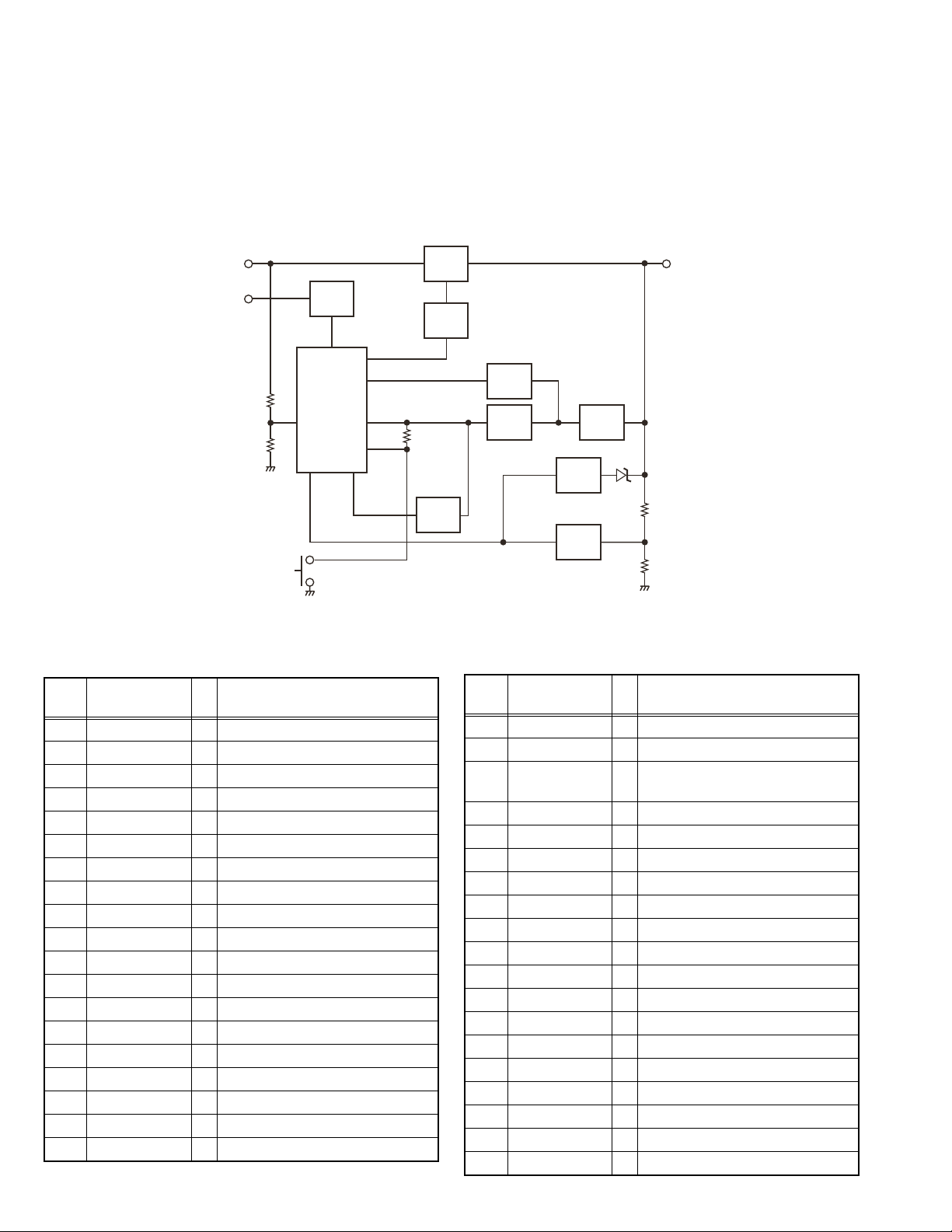
2.1 SYSTEM SET-UP
SECTION 1
PRECAUTION
This service manual does not describe PRECAUTION.
SECTION 2
SPECIFIC SERVICE INSTRUCTIONS
2.2 REALIGNMENT
2.2.1 Modes
User mode
PC mode
Merchandise received
Choose the type of transceiver
Transceiver programming
(Option)
KES-3
External speaker
Data programming mode
A personal computer, programming interface (KPG-46A/46U),
and FPU (programming software) are required for programming.
KCT-60
Connection cable
Extension cable
KCT-18
Ignition sense cable
Delivery
Frequency range (MHz)
136~174 25W NX-740 M
136~174
136~174
(Option)
KCT-36
(Option)
External speaker
RF power
50W
50W
(Option)
(Option)
KES-5
Type
NX-740H K
NX-740H(V) K
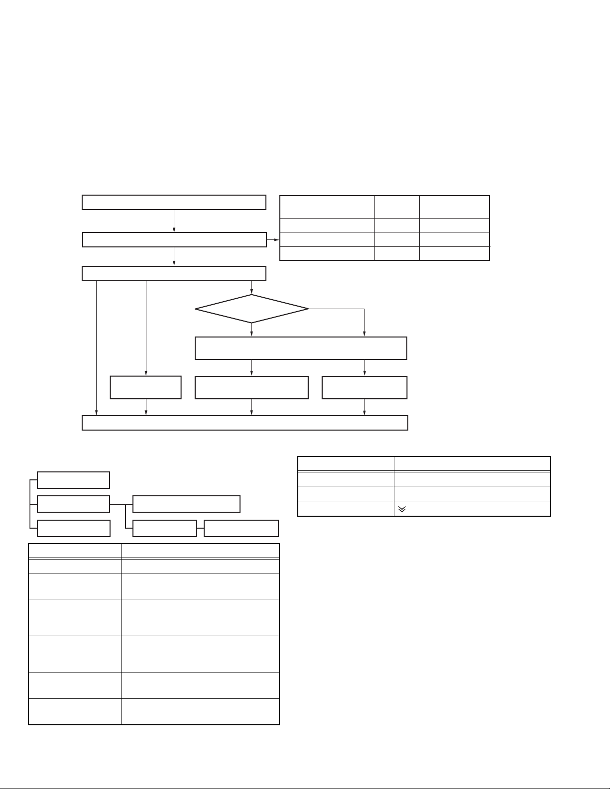
2.2.2 How to Enter Each Mode
Mode Function
User mode Power ON
PC mode Received commands from PC
Clone mode [ ] + Power ON (Two seconds)
Clone mode
PC test mode
PC tuning mode
Mode Function
User mode For normal use.
PC mode Used for communication between the
transceiver and PC (IBM compatible).
PC programming
mode
Used to read and write frequency data
and other features to and from the
transceiver.
PC test mode Used to check the transceiver using the
PC.
This feature is included in the FPU.
PC tuning mode Used to tune the transceiver using the
PC.
Clone mode Used to transfer programming data
from one transceiver to another.
1-4 (No.RA010<Rev.001>)
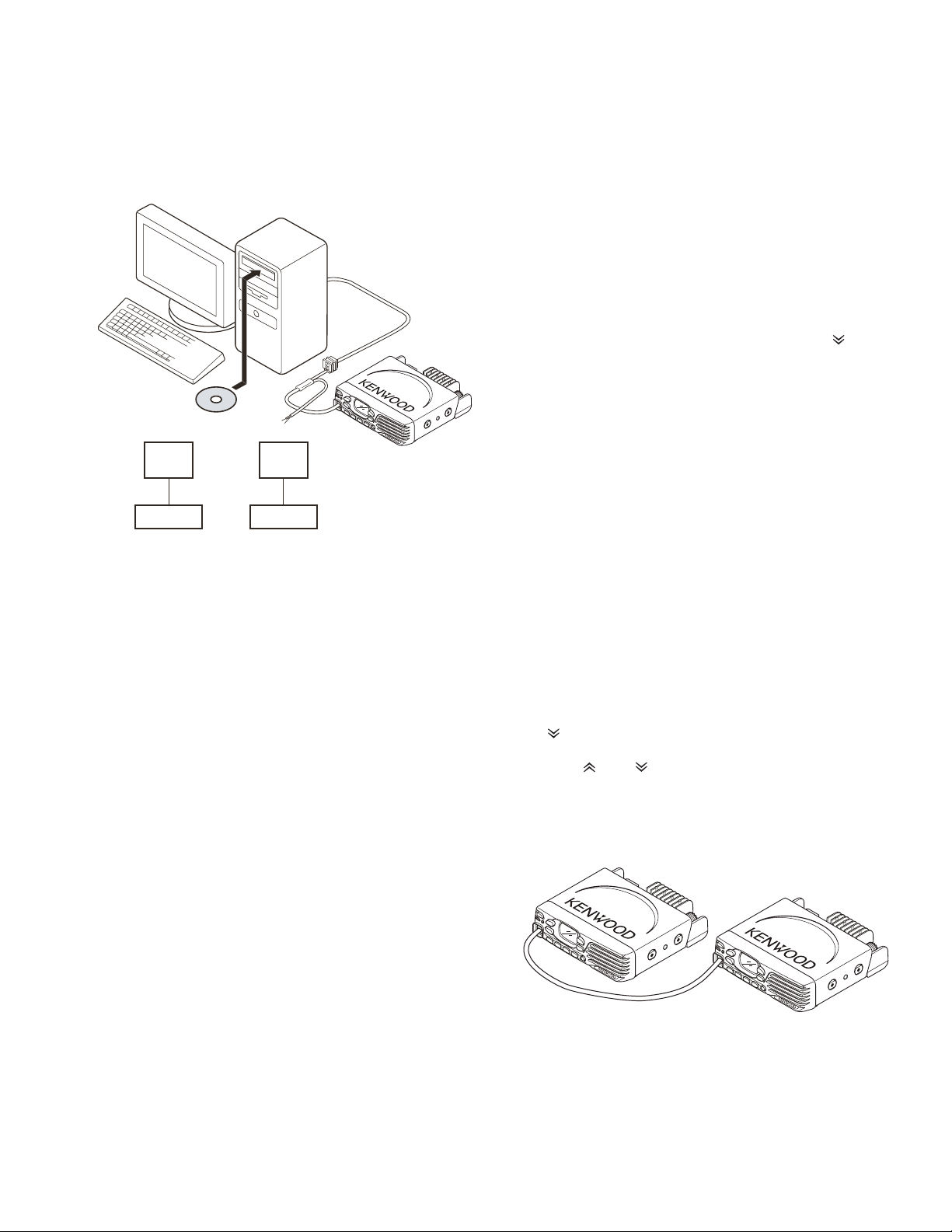
2.2.3 PC Mode
2.2.3.1 Preface
The transceiver is programmed using a personal computer, a
programming interface (KPG-46A/46U) and FPU (programming
software).
The programming software can be used with a PC. Figure 1
shows the setup of a PC for programming.
PC
KPG-46A or KPG-46U
+ Tuning cable
(E30-3383-05)
FPU
PC
D-SUB
(9-pin)
KPG-46A
Transceiver
PC
USB
KPG-46U
Transceiver
Fig.1
2.2.3.2 Connection procedure
(1) Connect the transceiver to the computer using the interface
cable.
Note:
You must install the KPG-46U driver in the computer to
use the USB programming interface cable (KPG-46U).
(2) When the Power is switched on, you can immediately enter
user mode. When the PC sends a command, the transceiver enters PC mode, and “Pc” is displayed on the LED.
When data is transmitting from the transceiver, the red LED
blinks.
When data is receiving by the transceiver, the green LED
blinks.
Note:
The data stored in the computer must match the “Model
Name” when it is written into the EEPROM.
2.2.3.3 KPG-46A description
(PC programming interface cable: Option)
The KPG-46A is required to interface the transceiver to the computer. It has a circuit in its D-sub connector (KPG-46A: 9-pin)
case that converts the RS-232C logic level to the TTL level.
The KPG-46A connects the 8-pin microphone connector of the
transceiver to the RS-232C serial port of the computer.
2.2.3.4 KPG-46U description
(USB programming interface cable: Option)
The KPG-46U is a cable which connects to a USB port on a computer.
When using the KPG-46U, install the supplied CD (with driver
software) in the computer. The KPG-46U driver runs under Windows XP, Vista, 7 or 8.
The latest version of the USB driver is available for download
from the following URL:
http://www.kenwood.com/usb-com/
(This URL may change without notice.)
2.2.3.5 Programming Software: KPG-175D description
The FPU is the programming software for the transceiver supplied on a CD. This software runs under Windows XP, Vista, 7 or
8 on a PC.
The data can be input to or read from the transceiver and edited
on the screen. The programmed or edited data can be printed
out. It is also possible to tune the transceiver.
2.2.4 Clone Mode
Programming data can be transferred from one transceiver to another by connecting them via their cloning cable. The operation
is as follows (the transmit transceiver is the source and the receive transceiver is a target).
Note:
Clone mode should be enabled.
(1) Turn the source transceiver power ON with the [ ] key held
down (2 seconds), “cL” is displayed on the LED.
(2) Power on the target transceiver.
(3) Connect the cloning cable (No. E30-3382-05) to the modu-
lar microphone jacks on the source and target.
(4) Press the [S] key on the source transceiver.
The data of the source is sent to the target. While the
source is sending data, red LED blinked.
While the target is receiving the data, “Pc” is displayed and
green LED blinked. When cloning of data is completed, the
source displays “En”, and the source red LED turned off,
and the target automatically operates in the User mode.
The target can then be operated by the same program as
the source.
(5) The other target can be continuously cloned. Carry out the
operation in step 2 to 4.
2.2.4.1 Adding the data password.
If the data password is set in the optional feature menu, you must
enter the password (Source transceiver) to activate a clone
mode.
You can use 0~9 to configure the password. The maximum
length of the password is 6 digits.
(1) [ ]+Power ON.
(2) “PS” is displayed on the LED.
(3) If the [ ] and [ ] keys is pressed while “PS” is displayed,
numbers (0 to 9) are displayed flashing. When you press
the [C>] key, the currently selected number is determined.
If you press the [S] key after entering the password in this
procedure, “cL” is displayed if the entered password is cor-
rect. If the password is incorrect, “PS” is redisplayed.
Cloning cable
(E30-3382-05)
Fig.2
(No.RA010<Rev.001>)1-5
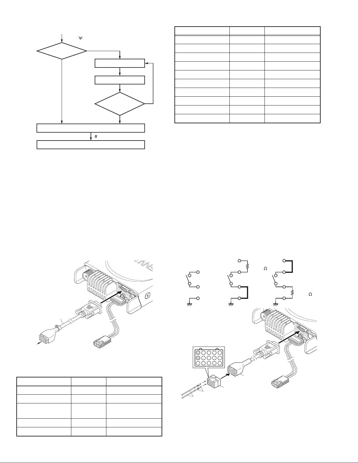
2.2.4.2 Flow chart (Source transceiver)
Press [ ] key + Power ON for 2 seconds
password*
* Read
Authorization
password
Is
set?
No
Start the clone funnction
Yes
Clone mode
[ ]
Shows PS
Enter password
Is entered
password
correct?
Yes
No
D-sub 15-pin Pin No. Name Molex 15-pin Pin No.
6 FNC1 9
7 FNC2 11
8 FNC3 7
9 FNC4 6
10 FNC5 8
11 FNC6 10
12 5MS NC
13 HR1 13
14 HR2 14
15 GND 3
2.3.2 Horn Alert Function
The Horn alert function (max. 2A drive) is enabled by installing
the KCT-60 in the transceiver.
2.3 INSTALLATION
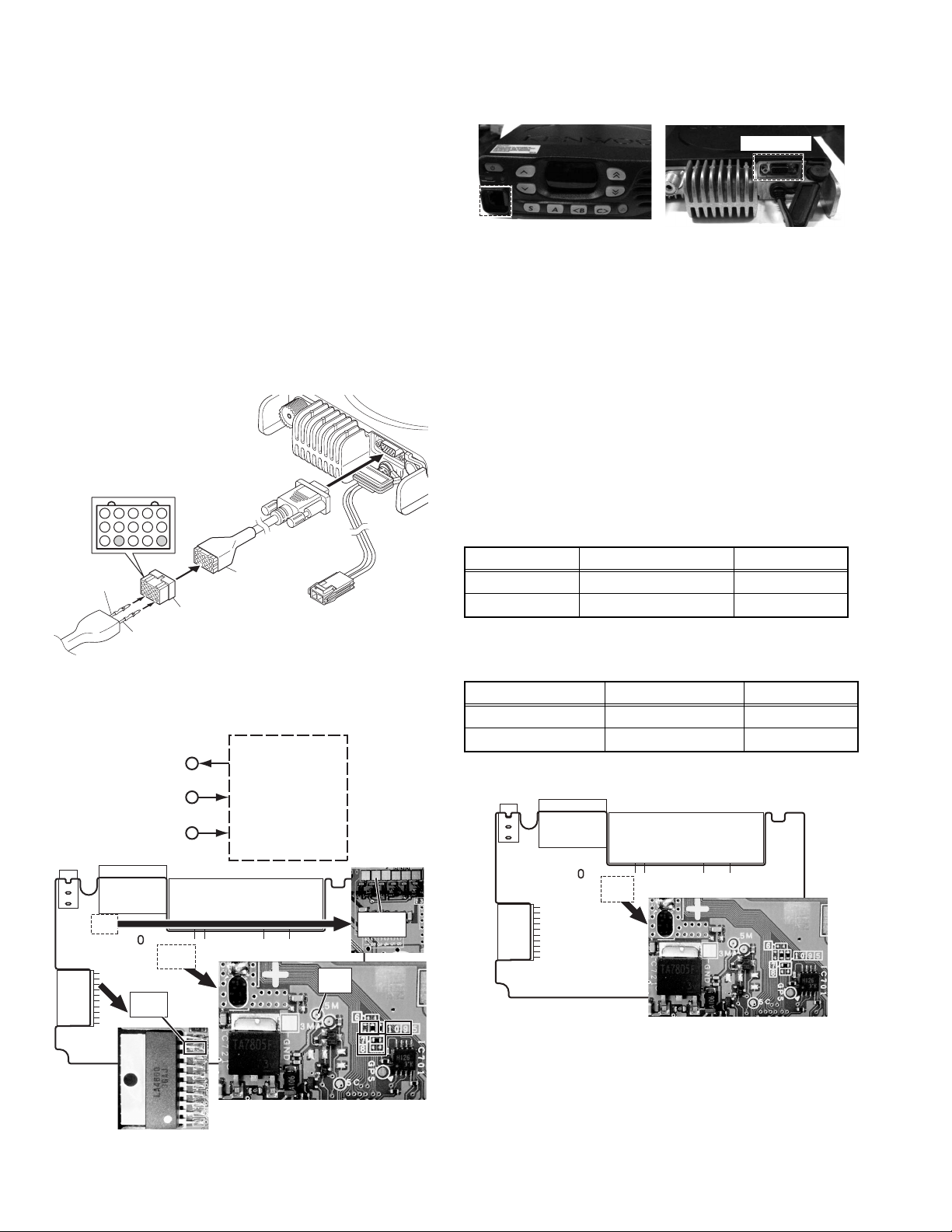
2.3.1 Connection Cable (KCT-60: Option)
The KCT-60 connection cable kit is used to connect the transceiver to a Horn alert cable, KCT-18 (Ignition sense cable), KES5 (External speaker), or through the KCT-36 extension cable.
2.3.1.1 Installing the KCT-60 (Connection cable) in the
transceiver
(1) Remove the ACC. cap on the rear of the transceiver.
(2) Connect the D-sub connector of the KCT-60 to the D-sub
15-pin terminal of the transceiver.
(3) Connect the 15-pin connector of the KCT-60 to a Horn alert
cable, KCT-18, KES-5, or through a KCT-36 extension cable.
Note:
You must set up using the KPG-175D.
KCT-60
2.3.2.1 Installation Procedure
(1) Remove the ACC. cap on the rear of the transceiver.
(2) Connect the D-sub connector of the KCT-60 to the D-sub
15-pin terminal of the transceiver.
(3) Insert the two crimp terminals of the Horn alert cable to pins
13 and 14 of the square plug.
(4) Connect the square plug to the 15-pin connector of the
KCT-60.
(5) Connect the remaining two Horn alert cables to your car
Horn alert signal control.
The internal FET switch can be controlled by turning the HA
function on/off and by using a signaling decode output. The
maximum current of HA is 2A. This FET switch is the open
drain circuit. Therefore, a DC power supply is necessary to
use the HR1. The voltage range is from 5V to 16V.
1. SB
13. HR1
14. HR2
3. GND
More
than 8
(Default)
13. HR1
14. HR2
3. GND
1. SB
More
than 8
13. HR1
14. HR2
3. GND
Horn alert cable, KCT-18,
KES-5 or through KCT-36
extension cable
2.3.1.2 Terminal function
D-sub 15-pin Pin No. Name Molex 15-pin Pin No.
1SB1
2IGN2
3 PA or
12
External SP
4DETO 4
5 DATAI 5
1-6 (No.RA010<Rev.001>)
13
10
7
4
14
11
15
12
13
Horn alert cable
1
8
5
2
9
6
3
14
Crimp terminal
KCT-60
Square plug
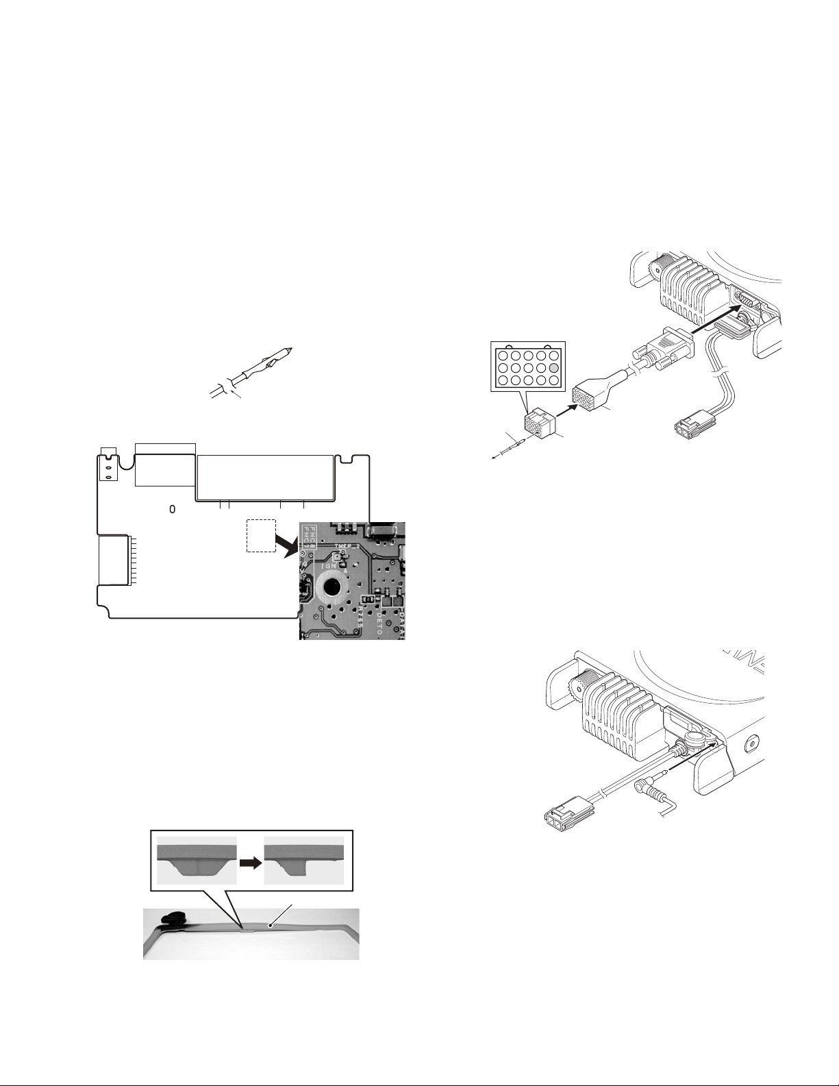
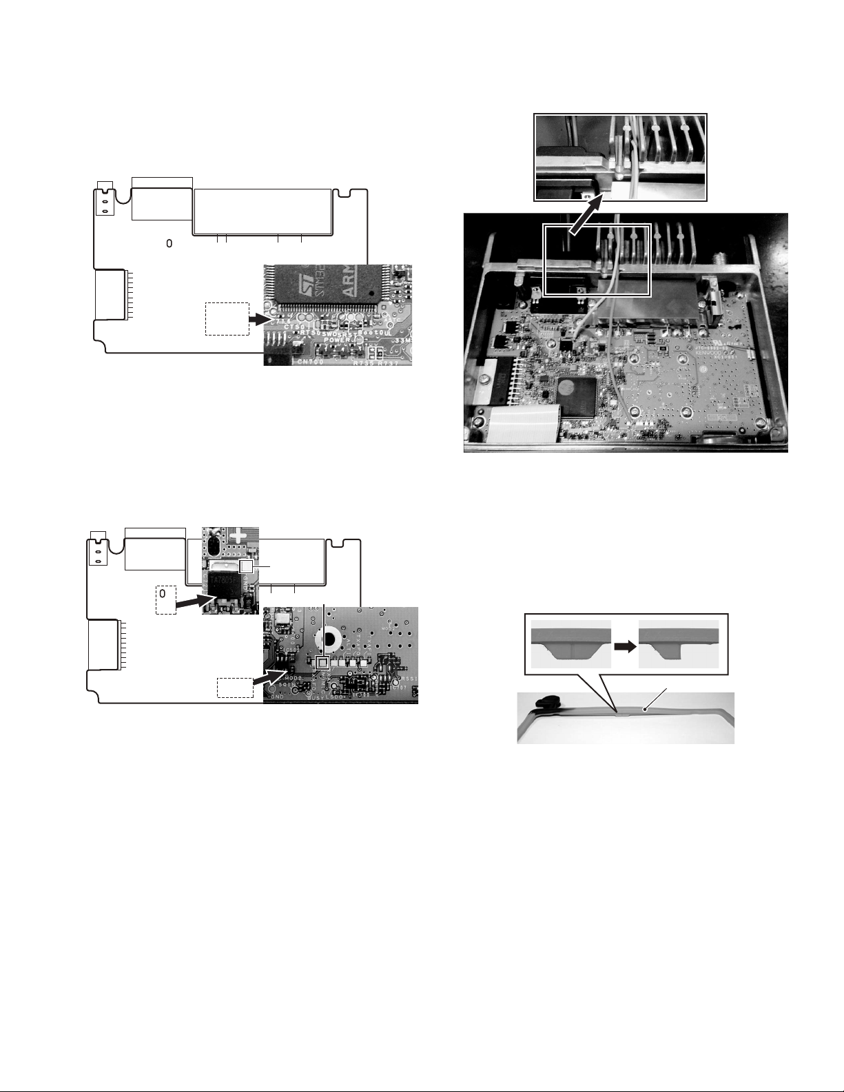
2.3.3 Ignition Sense Cable (KCT-18: Option)
The KCT-18 is an optional cable for enabling the ignition function. The ignition function lets you turn the transceiver power on
and off with the car ignition key.
2.3.3.1 Installing the KCT-18 (Ignition sense cable) in the
transceiver
(1) The KCT-18 can be installed in the transceiver by the fol-
lowing two methods (Method A, Method B).
Method A: The KCT-18 is soldered to the “IGN” pad on the
TX-RX unit.
Method B: The KCT-18 is connected to the 15-pin connector of the KCT-60 connected to the transceiver.
Installation Procedure: Method A
(1) Remove the two screws on both the right and left sides
of the transceiver, then remove the cabinet and top packing from the transceiver.
(2) Cut the crimp terminal side of the KCT-18 using a pair of
nippers or similar tool.
Cut
(3) Solder the cable side cut in the above step 3 to the “IGN”
pad on the TX-RX unit.
Installation Procedure: Method B
(1) Remove the ACC. cap on the rear of the transceiver.
(2) Connect the D-sub connector of the KCT-60 to the D-sub
15-pin terminal of the transceiver.
(3) Insert the crimp terminal side of the KCT-18 to pin 2 of
the square plug.
(4) Connect the square plug to the 15-pin connector of the
KCT-60.
(5) Connect the other side of the KCT-18 to the ignition line
of the car.
Note:
You must set up using the KPG-175D.
13
10
7
4
1
14
11
15
12
KCT-18
Ignition
line of the car
2
8
5
9
6
3
KCT-60
2
Square plug
TX-RX unit
Component side
(4) Dress the KCT-18 cable as shown in the figure. The
KCT-18 cable needs to pass through one of two indentations located on the rear panel of the transceiver.
(5) Cut off the projection of the top packing using a pair of
nippers or similar tool.
If the KCT-18 cable is dressed to be routed through the
indentations on the right side in step 5, the right side of
the projection needs to be cut off. If the KCT-18 cable is
dressed to be routed through the indentations on the left
side, the left side of the projection needs to be cut off.
Following is a figure presenting an example for when the
right side of the projection is cut off.
Top packing
2.3.4 External Speaker (Option)
2.3.4.1 KES-3
The KES-3 is an external speaker for the 3.5-mm-diameter
speaker jack.
Connection procedure
(1) Remove the speaker-jack cap on the rear of the trans-
ceiver.
(2) Connect the KES-3 to the 3.5-mm-diameter speaker jack
on the rear of the transceiver.
(6) Reinstall the top packing. Check the correct fitting of the
top packing, then reinstall the cabinet and two screws for
the right and left sides.
(7) Connect the other side of the KCT-18 to the ignition line
of the car.
(No.RA010<Rev.001>)1-7
2.3.4.2 KES-5
External speaker KES-5 can be installed for KCT-60.
Connection procedure
(1) Remove the ACC. cap on the rear of the transceiver.
(2) Connect the D-sub connector of the KCT-60 to the D-sub
15-pin terminal of the transceiver.
(3) Insert the two crimp terminals of the KES-5 to pins 3 and
12 of the square plug.
(4) Connect the square plug to the 15-pin connector of the
KCT-60.
Note:
• You must set up using the KPG-175D.
Before the external speaker can be used, you must assign
one of the keys as “External Speaker”, using the KPG175D.
• This also applicable to public address provide you must
assign one of the keys as “Public Address”, using the
KPG-175D.
13
10
7
4
11
8
12
9
12
Black lead
1
5
2
6
3
3
KCT-60
Square plug
14
15
Black/
White lead
2.3.5 GPS Receiver Connection
2.3.5.1 Connecting the GPS receiver
(1) Soldering position
TX-RX unit
FNC2
5M
DATA OUT
POWER
2.3.6 Extended Function: COM Port 0 and COM Port 1
Location of COM Port 0 and COM Port 1 of the transceiver is
shown below.
COM Port 1
COM Port 0
You must configure the transceiver COM Port 0 and COM Port 1
using the KPG-175D.
When you set as “Data”, the Function port 1 and 2 will be automatically fixed as Input ports.
The reason for this is because function port 1 (TXD) and 2 (RXD)
share the same circuit path of TXD and RXD line.
2.3.7 Changing Serial Port Level
2.3.7.1 Change FNC1 (TXD) and FNC2 (RXD) of D-SUB 15pin connector from TTL level to RS-232C level
FNC1 (TXD /6pin ) and FNC2 (RXD /7pin ) of D-SUB 15-pin connector are configured at the TTL level as the default value. But
you can change these serial port level to RS-232C level through
the RS-232C level converter IC (IC704) by configuring the port.
FNC1 (TXD)
Remove the R761 chip jumper and solder the clip jumper to
R767.
TTL level RS-232C level
R761[5] *1 0Ω chip jumper. open
R767[6] *1 open 0Ω chip jumper.
FNC2 (RXD)
Remove the R724 and R762 chip jumpers and solder the chip
jumpers to R725 and R756.
TTL level RS-232C level
R724[7], R762[9] *1 0Ω chip jumper. open
R725[8], R756[10] *1 open 0Ω chip jumper.
*1: The value in square bracket [ ] is the silk print number on
the TX-RX unit.
GND
TX-RX unit
Component side
GND
GROUND
GPS receiver
FNC2
5M
(2) Refer to FNC2 (RXD) of “2.3.7 Changing Serial Port Level”.
1-8 (No.RA010<Rev.001>)
TX-RX unit
Component side
2.3.8 Changing of Signal Type
MIC +ve cable (signal line)
MIC -ve cable (GND)
2.3.8.1 Change signal input of D-SUB connector from DI to
MIC
The input (5pin) of D-SUB 15-pin connector is configured at the
DI as the default value.
Remove the R737 chip jumper and solder the chip jumper to
R735.
TX-RX unit
Component side
2.3.9 Emergency MIC
2.3.9.1 Installation Procedure
(1) Remove the two screws on both the right and left sides of
the transceiver, then remove the cabinet and top packing
from the transceiver.
(2) solder the MIC connection cable as below
a) solder the MIC +ve cable (signal line) to EMGMIC
solder pad
b) solder the -ve cable (GND) to GND solder pad
MIC -ve cable (GND)
MIC -ve cable (GND)
MIC +ve cable (signal line)
MIC +ve cable (signal line)
(3) Dress the cable as shown in the figure. The cable needs to
pass through one of two indentations located on the rear
panel of the transceiver.
(4) Cut off the projection of the top packing using a pair of nip-
pers or similar tool.
If the cable is dressed to be routed through the indentations
on the right side in step 4, the right side of the projection
needs to be cut off.
If the cable is dressed to be routed through the indentations
on the left side, the left side of the projection needs to be
cut off.
Following is a figure presenting an example for when the
right side of the projection is cut off.
TX-RX unit
Component side
Note:
You must set up using the KPG-175D.
Top packing
(5) Reinstall the top packing. Check the correct fitting of the
top packing, then reinstall the cabinet and two screws for
the right and left sides.
(No.RA010<Rev.001>)1-9
2.4 CIRCUIT DESCRIPTION
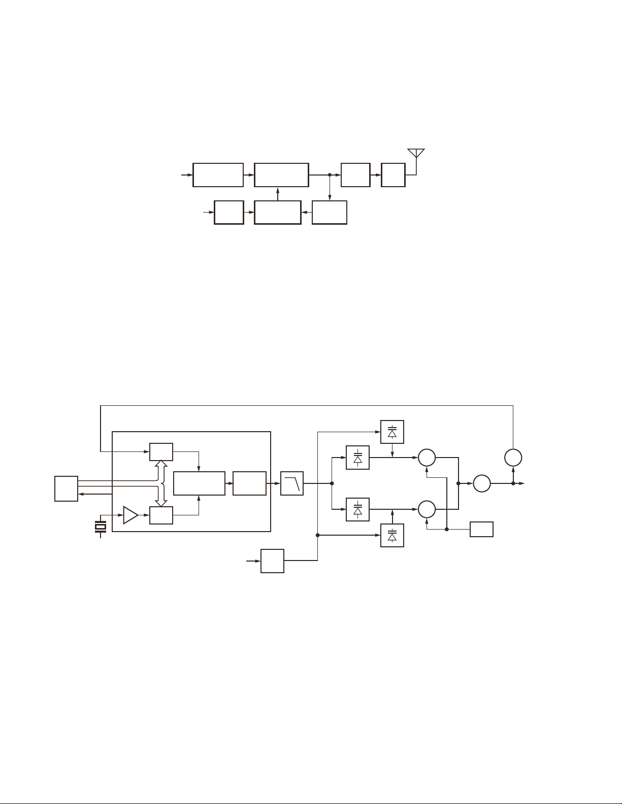
2.4.1 Frequency Configuration
The receiver utilizes double conversion. The first IF is 49.95MHz and the second IF is 450kHz. The first local oscillator signal is supplied from the PLL circuit.
The PLL circuit in the transmitter generates the necessary frequencies. Figure 1 shows the frequencies.
ANT
ANT
SW
RF
AMP
1st
MIX
MCF
49.95MHz
IF SYSTEM
50.4MHz
x3
Tripler
SP
AF
PA
16.8MHz
MIC
MIC
AMP
POWER
AMP
RF
AMP
TCXO
RX
PLL/VCO
TX
Fig.1 Frequency configuration
2.4.2 Receiver System
The receiver is double conversion superheterodyne.
The frequency configuration is shown in Figure 1.
D305,D306
D309,D310
ANT
SW
L512,L513
D504,D505
BPF
IC503
DC OP AMP
Q506
RF AMP
TV
TVC
L507,L508
D502,D503
BPF
OSC (VCO/PLL)
Q503
MIX
1st local
XF500
MCF
Q501
IF AMP
X1
TCXO
IC501
FM IC system
Q500
Tripler
IC709
Baseband IC
Fig.2 Receiver system
2.4.2.1 Front-end RF Amplifier
An incoming signal from the antenna is applied to an RF amplifier (Q506) after passing through a transmit/receive switch circuit (D305,
D306, D309 and D310) , BPF (L512, L513, and varactor diodes : D504, D505).
After the signal is amplified (Q506), the signal is filtered by a BPF (L507, L508 and varactor diodes : D502, D503) to eliminate unwanted signals before it is passed to the first mixer.
The voltage of these diodes are controlled by the TVC according to the channel frequency. (See Figure 2)
2.4.2.2 First Mixer
The signal from the RF amplifier is heterodyned with the first local oscillator signal from the PLL frequency synthesizer circuit at the
first mixer (Q503) to create a 49.95MHz first intermediate frequency (1st IF) signal. The first IF signal is then fed through one pair of
monolithic crystal filter (MCF : XF500) to further remove spurious signals.
2.4.2.3 IF Amplifier Circuit
The first IF signal is amplified by Q501, and the enters IC501 (FM processing IC). The signal is heterodyned again with a second local
oscillator signal within IC501 to create a 450kHz second IF signal. The second IF signal is fed through a 450 kHz filter in IC501 to
further eliminate unwanted signals before it is amplified and FM detected in IC501.
1-10 (No.RA010<Rev.001>)
2.4.2.4 AF Signal System
The detection signal from FM IC (IC501) goes to the baseband IC (IC709) DISC input (pin 16) after pass through IC500 for characterizing the signal.
• Analog signal
The demodulated AF signal pass through IC709 with the signal processing and output at AUDIO (pin26) to the E-Vol before the
Audio amplifier (IC719). The AF signal from IC719 switches between the internal speaker and speaker jack (J701) output.
• NXDN (Digital signal)
The recovered 4L-FSK signal obtained from IC501 is decoded in the baseband IC (IC709).
Decoded signal is fed into microprocessor (IC714) and converted to PCM audio signal, and return to baseband IC (IC709) for converting to audio signal.
This audio signal will output at AUDIO (pin26) to the E-Vol before the Audio amplifier (IC719).
The AF signal from IC719 switches between the internal speaker and speaker jack (J701) output.
IC501
IC500
IC709
IC715
IC719
FM IC
AMP
Baseband IC
MCU
(Build in Vocoder)
E-Vol
IC714
AF PA
Fig.3 AF signal system
2.4.2.5 Squelch Circuit
Part of the AF signal goes a rectifier circuit to produce a DC voltage corresponding to the noise level after filtering and amplification.
This DC voltage send to MCU (IC714) SQIN input pin.
The MCU controls squelch according to the voltage (SQIN) level.
The signal from the RSSI pin of IC501 is monitored. The electric field strength of the receive signal can be known before the SQIN
voltage is input to the MCU, and the scan stop speed is improved.
Q500
Noise DET
SQIN
IC714
MCU
RSSI
IC501
FM IC
NAMPO
RSSI
Q502
Noise
AMP
Fig.4 Squelch circuit
2.4.3 Transmitter System
2.4.3.1 Outline
The transmitter circuit produces and amplifies the desired frequency directly. It FM-modulates the carrier signal by means of a varicap
diode.
ANT
IC706MIC
MIC
AMP
D712, Q701
SW
IC709
Baseband
IC
Q7
TX
VCO
Q11
BUFF
AMP
Q12
RF
AMP
Q300 IC300
DRIVE
AMP
RF POWER
module
MIC key
input
MCU
IC714
TCXO
16.8MHz
X1
PLL IC
IC2
RF
AMP
Q2
Fig.5 Transmitter system
2.4.3.2 Power Amplifier Circuit
The transmit output signal from the VCO passes through the transmission/reception selection diode (D16) and amplified by Q300.
The amplified signal goes to the RF power module (IC300) through a low-pass filter.
The lowpass filter removes unwanted high-frequency harmonic components, and the resulting signal is goes the antenna terminal.
(No.RA010<Rev.001>)1-11
2.4.3.3 APC Circuit
The automatic transmission power control (APC) circuit detects part of a final amplifier output with a coupler circuit and applies a voltage to IC301.
IC301 compares the APC control voltage (APCC) generated by the baseband IC (IC709) and DC amplifier (IC503) with the detection
output voltage.
IC301 generates the voltage to control IC300 and stabilizes transmission output.
The APC circuit is configured to protect over current of Q300 and IC300 due to fluctuations of the load at the antenna end and to
stabilize transmission output at voltage and temperature variations.
ANT
LPF
D16
DRIVE AMP
IC300Q300
RF POWER
MODULE
D305,D306
D309,D310
ANT
SW
APCC
IC709
pin 32
DC
AMP
IC503
APC
control
IC301
Coupler
circuit
Fig.6 APC circuit and Power amplifier circuit
2.4.4 PLL Frequency Synthesizer
The PLL circuit generates the first local oscillator signal for reception and the RF signal for transmission.
2.4.4.1 PLL Circuit
The frequency step of the PLL is 2.5, 5.0, 6.25 or 7.5 kHz. A 16.8MHz reference signal is divided at IC2 by a fixed counter to produce
the reference frequency.
The voltage controlled oscillator (VCO) feedback output is divided by a programmable counter in IC2.
The 2 signals are phase compared, filtered through a low pass filter and passed to VCO to control the oscillator frequency.
2.4.4.2 VCO Circuit
The operating frequency is generated by Q7 in transmit mode and Q5 in receive mode.
The oscillator frequency is controlled by applying the control voltage, which obtained from the phase comparator, to varactor diodes
(D5, D6, D9, D10, D11 in transmit mode and D7, D8, D12, D13, D14 in receive mode).
The TX/RX pin is set “High” in receive mode causing turn on Q9. And T/R pin is set “Low” in transmit mode causing turn on Q6.
D9,D10,D11
PLL_DATA
MCU
PLL_UL
16.8MHz
IC2: PLL IC
REF
OSC
1/N
1/M
Phase
comparator
Charge
ASTC
pump
IC2
OP
AMP
LPF
D5,D6
D7,D8
Assist
voltage
D12,D13,D14
Q7
TX VCO
Q5
RX VCO
Q11
BUFF
AMP
Q6,Q9
T/R SW
Q2
AMP
Fig.7 PLL and VCO circuit
2.4.4.3 Unlock Circuit
If low level appears at the “LD” pin of IC2, then PLL an unlock condition occurs.
It causes the voltage applied to the “PLL_UL” pin of the microprocessor to go low.
When the microprocessor detects this condition, the transmitter is disabled by ignoring the push-to-talk switch input signal.
1-12 (No.RA010<Rev.001>)
2.4.5 Control Circuit
The MCU carries out the following tasks:
(1) Controls the FM IC (IC501).
(2) Controls the baseband IC (IC709).
(3) Controls the PLL (IC2) & TX/RX outputs.
(4) Controls IO expender through I2C level converter.
(5) Controls the display unit.
PLL IC
PLL_U
PLL_PDN2
PDN
RSTN
IC501
FM IC
CSN
SCLK
SDATA
BLED
RLED
GLED
IC714
MCU
MBL
Fig.8 Control circuit
2.4.5.1 Memory Circuit
The transceiver has an 256k-bit EEPROM (IC716). The EEPROM contains adjustment data. The MCU (IC714) controls the
EEPROM through three serial data lines.
IC2
PLL_CLK
PLL_DATA
PLL_LE
LECI
LECE
LECL
IC1
LED Driver
Display unit
LELH
C.DATA
R.DATA
SCLK
IRQ
CSN
converterIOexpender
IC714
MCU
IC709
Baseband
I2C level
IC700 IC702
EEP_DATAO
EEP_CLK
EEP_DATAI
EEP_CS
EEP_WP
IC716
EEPROM
2.4.5.2 Display Circuit
The MCU (IC714) controls the Display 7-segment LED and
LEDs.
When power is on, the MCU will use the MBL line to control the
key backlight LEDs.
When the transceiver is busy, the GLED line goes high, Q1 turns
on and the green LED (D23) lights after Q4 turn on. In transmit
mode, the RLED line goes high, Q2and Q8 turns on and the red
LED (D23) lights.
BLED will be set high when the function select (FPU setting) is
on, Q6 turn on and the blue LED (D22) lights.
The dimmer function is controlled by the switch Q5. The LED
driver (IC1) controls the functions of the 7-segment LED through
the LEDI, LECE, LECL, LELH lines from the MCU.
IC714
MCU
Fig.9 Memory circuit
LEDM
LEDI
LECE
LECL
LELH
MBL
GLED
RLED
BLED
Q5
SW
IC1
LED
driver
Q3
SW
Q1
SW
Q2
SW
Fig.10 Dsplay circuit
Q4
SW
Q7
SW
Q8
SW
Q6
SW
Display
7-segment
D1~D5
Key backlight
D23
D22
(No.RA010<Rev.001>)1-13
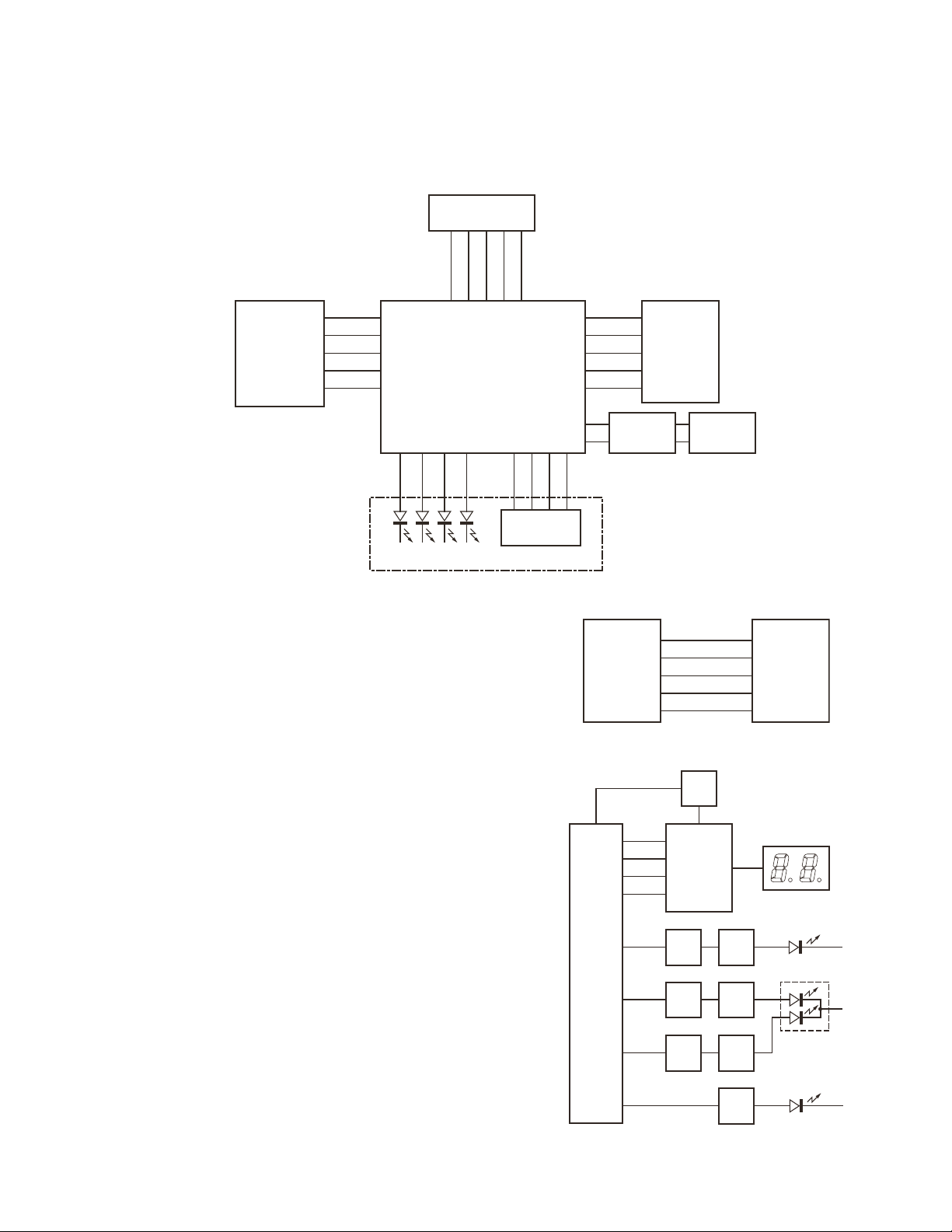
2.4.5.3 Key Matrix Circuit
The front panel has function keys. Each of them is connected to
KMO1
<
B
A
a cross point of a matrix of the KMI1 to KMO3 ports of the microprocessor.
The KMO1 to KMO3 ports are always high, while the KMI1 to
KMI3 ports are always low.
The microprocessor monitors the status of the KMI1 to KMO3
ports. If the state of one of the ports changes, the microprocessor
assumes that the key at the matrix point corresponding to that
port has been pressed.
IC714
MCU
KMO2
KMO3
KMI3
KMI2
KMI1
CH UP
VOL DN
VOL UP
Fig.11 Key matrix circuit
2.4.6 Signaling Circuit
2.4.6.1 Encode
(1) Low-speed data (QT, DQT)
Low-speed data is output from pin 40 (LSDO) of the MCU (IC714).
The signal passes through a low-pass CR filter. The signal is mixed with the audio signal and goes to the VCO and TCXO (X1)
modulation input after signal processing in the baseband IC (IC709).
(2) High-speed data (2-tone)
High-speed data (HSD) is output from pin 41 (HSDO) of the MCU.
The signal passes through a low-pass CR filter. TX deviation making an adjustment by microprocessor is applied to the baseband IC (IC709).
The signal is mixed with the audio signal and goes to the VCO and TCXO.
The side tone is audio ouput of baseband IC(IC709) at the same time to audio power amplifier and then to the speaker.
(3) MSK / DTMF
MSK and DTMF signal is self genarated by the baseband IC(IC709).
The TX deviation adjustment is done by the output gain of baseband IC(IC709), and is routed to the VCO.
When encoding MSK/DTMF, the microphone-input signal is muted.
TCXO
MOD
VCO
MOD
X1
TCXO
IC1
PLL
VCO
IC714
MCU
LSDO
QT/DQT
HSDO
2-TONE
IC709
Baseband IC
DTMF/
MSK
Fig.12 Encode
S
C
>
CH DN
2.4.6.2 Decode
(1) Low-speed data (QT, DQT)
The demodulated signal from the FM IC (IC501) will input to baseband IC(IC701) to remove frequency above 300Hz.
The signal is input to pin 26(LSDI) of the MCU.
The MCU digitizes this signal, performs processing such as DC restoration, and decodes the signal.
(2) High-speed data (2-tone)
The demodulated signal from the FM IC (IC501) is amplified by baseband IC and passes through a band-pass filter in IC709 to
remove frequency of 3kHz or above and 300Hz or below.
The MCU digitizes this signal anddecodes the signal after receive the signal at pin 27(HSDI).
(3) MSK / DTMF
The demodulated signal from theFM IC(IC501) will input to baseband IC(IC709), then the baseband IC will decode and send the
decode information to MCU by the data line.
The MCU then processes the decoded information.
REPLAY data
DTMF/MSK
decode data
LSDI
QT/DQT
HSDI
2-TONE
IC714
MCU
IC501
FM IC
IC709
Baseband IC
DTMF/MSK
decode
Fig.13 Decode
1-14 (No.RA010<Rev.001>)
2.4.6.3 NXDN Receiving
r
r
• For Digital Data Mode:
The demodulated signal from IC501 (Pin13) feed into baseband IC (Pin 16) for NXDN decoding.
The decoded digital data will pass to MCU through C-BUS. MCU determines whether or not to output sound from speaker by checking if the data match.
• For Digital Voice Mode:
If the digital data match in MCU, the digital voice payload data will goes into Vocoder in MCU for conversion to PCM.
The PCM data will go to baseband IC through SPI input, where it will be converted to analog by DAC.
Analog voice will be filtered and finally send to audio amplifier.
IC501
IF IC
IC709 Baseband IC
1613
NXDN
decoder
Audio
Output
C-BUS
SPI
DAC
7543
3
112
IC714 MCU
C-BUS
Vocode
To E-Vol
Fig.14 NXDN receiver system
2.4.6.4 NXDN Transmitting
• For Digital Data Mode:
The digital data will be generated by MCU, where it wil be pass to baseband IC, through C-BUS for encoding process. The encoded
data finally will transmit through TCXO and VCO modulation.
• For Digital Voice Mode:
The analog voice from mic will go to ADC (after audio filter) to convert to PCM data.
The PCM data will send to Vocoder through SPI output.
Vocoder will convert the PCM to NXDN protocol, where it will be sent to baseband through C-BUS.
In baseband IC, the data will be encoded and finally transmit through TCXO and VCO modulation.
TCXO
VCO
IC709 Baseband IC
23
NXDN
encoder
24
Audio
Filter
C-BUS
SPI
ADC
7642
1
113
IC714 MCU
C-BUS
Vocode
From MIC
Fig.15 NXDN transmit system
(No.RA010<Rev.001>)1-15
2.4.7 Power Supply Circuit
• When the power switch on the display unit is pressed, the power port on the display unit which is connected pin 140 (POWKEY),
goes low, then pin88 (SBC) goes high, Q718 turns on, SB SW (Q719) turns on and power (SB) is supplied to the transceiver.
• When the DC power supplied to the transceiver, the voltage regulator IC (IC720&IC718) and supply into the MCU VDD and reset
voltage detect IC (IC723). IC723 will generate signal (RESET) into the reset terminal on the MCU (IC714) to carry out a power on
reset.
• When the DC power voltage deceases from normal voltage, the INT voltage detector IC (IC722) will set to high on MCU port 141
(BATT_INT). If B line becomes less than about 8.5V, MCU will send the backup data to EEPROM (IC716) and go into STOP mode.
This circuit has an overvoltage protection circuit. If a DC voltage of 18V or higher is applied to the base of Q712, this voltage turns
Q712 on and sets port 141 (BATT_INT) to low. As a result port 88 (SBC) is low, and turns Q719 and Q720 (SB) off.
SB
SW
Q706
SW
IGN
IC714
MCU
BATT
POWKEY
SBC
33MA
33MD
RESET
BATT_INT
IGN
R898
R899
POWER
Fig.16 Power supply circuit
2.5 SEMICONDUCTOR DATA
2.5.1 MCU: 2F405ZGT6KFKA (TX-RX unit IC714)
Pin
Port Name I/O Function
No.
1 LEDI O LED Data
2 LECE O LED Enable
3 LECL O LED Clock
4 LELH O LED Latch
5 LERE O LED Reset
6 VBAT - 3.3V
7 ACR_SW O ACR switch for HSDO(D/A) port
8 NC I No connection
9 NC I No connection
10 I2CDT I/O Function P8I/O Expander I2C Data
11 I2CCK I/O Function P7I/O Expander I2C Data
12 EVOL_DACCE O Function P6CE for EVOL
13 EVOL_SCLK O Function P5CLK for EVOL
14 EVOL_DATA O Function P4DATA for EVOL
15 /INT15P I/O Function P3I/O Expander Interrupt
16 VSS - GND
17 VDD - 33MD
18 BEEP O Beep for Side Tone
19 NC I No connection
Q719
SW
Q718
SW
IC723
AV R
B
IC720
AV R
Pin
IC718
AV R
Port Name I/O Function
Q712
SW
IC722
AV R
IC721
AV R
D715
R969R970
No.
20 PCBVER I PCB version identification
21 IFDET I IFDET for ACR improvement
22 DISC_DC
(optional)
I for Discriminator DC Level
Adjustment
23 XIN I Crystal (19.2MHz)
24 NC I No connection
25 RESET I MCU Reset pin
26 LSDI I Low-Speed Data Input
27 HSDI I High-Speed Data Input
28 TEMP_1 I Temperature 1
29 TEMP_2 I Temperature 2
30 VDD - 33MD
31 VSSA - GND
32 VREF+ - 33MA
33 VDDA - 33MA
34 TEST_TX I/O UART_TX for Debug
35 TEST_RX I/O UART_RX for Debug
36 FNC_1(TXD0) I/O Function P1(TXD)
37 FNC_2(RXD0) I/O Function P2(RXD)
38 VSS - GND
1-16 (No.RA010<Rev.001>)

Pin
No.
Port Name I/O Function
39 VDD - 33MD
40 LSDO O Low-Speed Data Output
41 HSDO O High-Speed Data Output
42 3CC O 33C Control
43 5CC O 5C Control
44 SQIN I Squelch Input
45 RSSI I RSSI Input
46 BATT I Battery Voltage
47 CVIN I VCO Lock Voltage
48 BOOT_1 I Test Point to enable Bootloader
49 TEST_1 I/O Test Point 1 for Debug
50 TEST_2 I/O Test Point 2 for Debug
51 VSS - GND
52 VDD - 33MD
53 PLL_DATA O PLL IC Data
54 PLL_LE O PLL IC Enable
55 PLL_CLK O PLL IC Clock
56 PLL_PDN2 O PLL IC Power Down
57 PA O Public Address
58 AMP_SW O AF amplifier
59 9TC O 9T Control
60 BSFT O Beat Shift
61 VSS - GND
62 VDD - 33MD
63 KMO3 O Key Matrix Output 3
64 KMO2 O Key Matrix Output 2
65 KMO1 O Key Matrix Output 1
66 KMI1 I Key Matrix Input 1
67 KMI2 I Key Matrix Input 2
68 KMI3 I Key Matrix Input 3
69 TXD2 O 2nd UART for DE15
70 RXD2 I 2nd UART for DE15
71 VCAP_1 - 2.2uF
72 VDD - 33MD
73 CML_CSN O C-BUS Chip Select
74 CML_SCLK O C-BUS Clock
75 CML_RDATA I C-BUS Reply Data
76 CML_CDATA O C-BUS Command Data
77 EEP_DATAO O EEPROM Data Out
78 EEP_DATAI I EEPRON Data In
79 EEP_SCLK O EEPROM Clock
80 EEP_CS O EEPROM Chip Select
81 EEP_WP O EEPROM Write Protect
82 BUCNT1 O PTT/TXD buffer control
83 VSS - GND
Pin
No.
84 VDD - 33MD
85 MKEYI I DTMF MIC key input
86 BUCNT2 O DTMF MIC buffer control
87 PLL_UL I PLL Unlock Detect
88 SBC O SB Control
89 MKEYO O DTMF MIC Key output
90 9RC O 9R Control
91 PTT I PTT
92 HOOK I Hook
93 ASTSW O Assist Speed-up Switch
94 VSS - GND
95 VDD - 33MD
96 FM_SDATA O FM IC Data In/Out
97 FM_RSTN O FM IC Hardware Reset
98 FM_SCLK O FM IC Clock
99 FM_CSN O FM IC Chip Select
100 FM_PDN O FM IC Power Down
101 TXD O Serial Data to Mic Jack
102 RXD I Serial Data from Mic Jack
103 TXRX O TX / RX Switch
104 HORN O Horn Alert
105 SWDIO I/O SWDIO for SWD
106 VCAP2 - 2.2uF
107 VSS - GND
108 VDD - 33MD
109 SWCLK I/O SWCLK for SWD
110 CML_SSOUT I Audio Codec Chip Select
111 CML_EPSCLK I Audio Codec Clock
112 CML_EPSO O Audio Codec Data Out
113 CML_EPSI I Audio Codec Data In
114 NC I No connection
115 LEDM O LED Dimmer
116 MBL O Panel and Mic Key Backlight
117 FNC_4 (CTS0) I Function P4(CTS)
118 FNC_3(RTS0) O Function P3(RTS)
119 NC I No connection
120 VSS - GND
121 VDD - 33MD
122 33BC O BB IC power supply control
123 MIC1MUTE O Internal Mic Mute
124 MIC2MUTE O External Mic Mute
125 SP_MUTE O Speaker Mute
126 SIM1 I Shimuke port 1
127 SIM2 I Shimuke port 2
128 NC O No connection
Port Name I/O Function
(No.RA010<Rev.001>)1-17
 Loading...