

Kenwood NX-5200, NX-5200 E2, NX-5200 K2, NX-5200 F3, NX-5200 K3 Service Manual
...
RA018<Rev.002>20159SERVICE MANUALB5B-7164-10
This service manual has been revised due to the addition of NX-5200 type E, E2.
REVISED
This product uses Lead Free solder.
SERVICE MANUAL
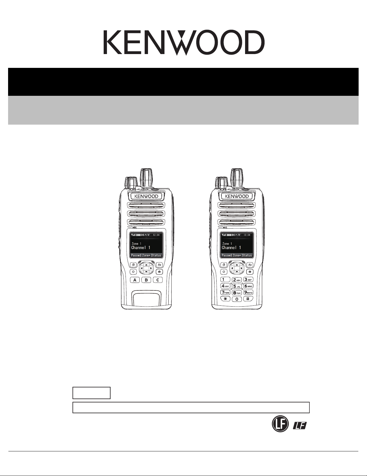
VHF DIGITAL TRANSCEIVER
NX-5200
NX-5200 F3,K3,ENX-5200 F2,K2,E2
COPYRIGHT © 2015 JVC KENWOOD Corporation
TABLE OF CONTENTS
1 PRECAUTION. . . . . . . . . . . . . . . . . . . . . . . . . . . . . . . . . . . . . . . . . . . . . . . . . . . . . . . . . . . . . . . . . . . . . . . . . 1-7
2 SPECIFIC SERVICE INSTRUCTIONS . . . . . . . . . . . . . . . . . . . . . . . . . . . . . . . . . . . . . . . . . . . . . . . . . . . . . . 1-7
3 DISASSEMBLY . . . . . . . . . . . . . . . . . . . . . . . . . . . . . . . . . . . . . . . . . . . . . . . . . . . . . . . . . . . . . . . . . . . . . . 1-27
4 ADJUSTMENT . . . . . . . . . . . . . . . . . . . . . . . . . . . . . . . . . . . . . . . . . . . . . . . . . . . . . . . . . . . . . . . . . . . . . . . 1-34
5 TROUBLESHOOTING . . . . . . . . . . . . . . . . . . . . . . . . . . . . . . . . . . . . . . . . . . . . . . . . . . . . . . . . . . . . . . . . . 1-94
B5B-7164-10
COPYRIGHT © 2015 JVC KENWOOD Corporation
No.RA018<Rev.002>
2015/9

Document Copyrights
TMTMR
Copyright 2015 by JVC KENWOOD Corporation. All rights reserved.
No part of this manual may be reproduced, translated, distributed, or transmitted in any form or by any means, electronic, mechanical, photocopying, recording, or otherwise, for any purpose without the prior written permission of JVC KENWOOD Corporation.
Disclaimer
While every precaution has been taken in the preparation of this manual, JVC KENWOOD Corporation assumes no responsibility
for errors or omissions. Neither is any liability assumed for damages resulting from the use of the information contained herein.
JVC KENWOOD Corporation reserves the right to make changes to any products herein at any time for improvement purposes.
Firmware Copyrights
The title to and ownership of copyrights for firmware embedded in KENWOOD product memories are reserved for JVC KENWOOD
Corporation. Any modifying, reverse engineering, copy, reproducing or disclosing on an Internet website of the firmware is strictly
prohibited without prior written consent of JVC KENWOOD Corporation. Furthermore, any reselling, assigning or transferring of the
firmware is also strictly prohibited without embedding the firmware in KENWOOD product memories.
Transceivers containing AMBE+2 Vocoder:
The AMBE+2 voice coding technology is embedded in the firmware under the license of Digital Voice Systems, Inc.
Bluetooth Copyrights
The Bluetooth word mark and logos are registered trademarks owned by Bluetooth SIG, Inc. and any use of such marks by
JVC KENWOOD Corporation is under licence. Other trademarks and trade names are those of their respective owners.
NOTE
• This equipment should be serviced by only qualified technicians.
• Danger of explosion if the battery is incorrectly replaced; replace only with the same type.
• To dispose of batteries, be sure to comply with the laws and regulations in your country or region.
Service Manual List
Manual number Model name Type Serial number Main unit number Remarks
No.RA018<Rev.001> NX-5200 F2,F3,K2,K3 -
F2,F3,K2,K3 From B5910001 XC1-0331-80/
No.RA018<Rev.002> NX-5200
E,E2 -
XC1-0331-80
(J79-0410-09)
XC1-0360-10
(J79-0410-19)
First edition
Revised
This service manual
1-2 (No.RA018<Rev.002>)
SPECIFICATION
(F2,F3,K2,K3 TYPE)
GENERAL
Frequency Range 136 ~ 174 MHz
Max. Channels per Radio 1024 (Up to 4000 CH with option)
Number of Zones 128
Max. Channels per Zone 512
Channel Spacing Analog 12.5 / 15 / 20 / 25* / 30* kHz
Digital 6.25 / 12.5 kHz
Operating Voltage 7.5V DC±20%
Battery Life 5-5-90
(10-10-80) duty cycle
Operating Temperature Range -22°F ~ +140°F (-30°C ~ +60°C)
Frequency Stability ±2.0ppm
Antenna Impedance 50Ω
Dimensions (W x H x D)
(Projections not included)
Weight (net) KNB-L1(2,000mAh) 13.5 oz (382 g)
RECEIVER
Sensitivity NXDN 6.25kHz Digital(3%BER) 0.20μV
Selectivity P25 Digital 60dB
Intermodulation 73dB
Spurious Rejection 80dB
Audio Distortion Less than 3%
Audio Output 3% Distortion 500mW / 8Ω
TRANSMITTER
RF Power Output 6W to 1W
Spurious Emission -70dB
KNB-L1(2,000mAh) 10 hours (6.5 hours)
KNB-L2(2,600mAh) 12.5 hours (8.5 hours)
KNB-L3(3,400mAh) 17 hours (11 hours)
KNB-N4(2,500mAh) 12.5 hours (8.5 hours)
KBP-8(w/AA x 12) High Power Approx. 11 hours (8 hours)
Low Power Approx. 25 hours (18 hours)
KNB-L1(2,000mAh) 2.28 x 5.47 x 1.57 in. (58.0 x 138.9 x 39.8 mm)
KNB-L2(2,600mAh) 2.28 x 5.47 x 1.69 in. (58.0 x 138.9 x 42.8 mm)
KNB-L3(3,400mAh) 2.28 x 5.47 x 1.90 in. (58.0 x 138.9 x 48.2 mm)
KNB-N4(2,500mAh) 2.28 x 6.55 x 1.91 in. (58.0 x 166.4 x 48.5 mm)
KBP-8 2.64 x 8.59 x 1.76 in. (67.0 x 218.3 x 44.6 mm)
KNB-L2(2,600mAh) 14.3 oz (406 g)
KNB-L3(3,400mAh) 15.8 oz (449 g)
KNB-N4(2,500mAh) 20.4 oz (579 g)
KBP-8(w/AA x 12) Approx. 25.1 oz (712 g)
NXDN 12.5kHz Digital(3%BER) 0.25μV
P25 Digital (5% BER) 0.25μV
P25 Digital (1% BER) 0.40μV
Analog (12dB SINAD) 0.25μV
Analog@12.5kHz 67dB
Analog@25kHz 73dB
5% Distortion 1000mW / 8Ω
(No.RA018<Rev.002>)1-3

FM Hum & Noise Analog @ 25 kHz 45dB
Analog @ 12.5 kHz 40dB
Audio Distortion Less than 2%
Modulation 16K0F3E, 11K0F3E, 8K10F1E, 8K10F1D, 8K10F1W,
8K30F1E, 8K30F1D, 8K30F7W, 4K00F1E,4K00F1D,
4K00F7W, 4K00F2D
*25 and 30 kHz are not included in the models sold in the USA or US territories.
Analog measurements made per TIA 603 and specifications shown are typical.
P25 Digital measurements made per TIA 102CAAA and specifications shown are typical.
JVC KENWOOD Corporation reserves the right to change specifications without prior notice or obligation.
1-4 (No.RA018<Rev.002>)
SPECIFICATION
(E,E2 TYPE)
GENERAL
Frequency Range 136 ~ 174 MHz
Max. Channels per Radio 1024 (Up to 4000 CH with option)
Number of Zones 128
Max. Channels per Zone 512
Channel Spacing Analogue 12.5 / 20 / 25 kHz
Digital 6.25 / 12.5 kHz
Operating Voltage 7.5V DC±20%
Battery Life 5-5-90
(10-10-80) duty cycle
NEXEDGE
Operating Temperature Range -30°C to +60°C
Frequency Stability ±2.0ppm
Antenna Impedance 50Ω
Dimensions (W x H x D)
(Projections not included)
Weight (net) KNB-L1(2,000mAh) 382 g
RECEIVER
Sensitivity Analogue
Selectivity P25 Digital 63dB
Intermodulation Analogue 65dB
Spurious Rejection Analogue 75dB
Audio Distortion Less than 3%
Audio Output 3% Distortion 500mW / 8Ω
KNB-L1(2,000mAh) 10 hours (6.5 hours)
KNB-L2(2,600mAh) 12.5 hours (8.5 hours)
KNB-L3(3,400mAh) 17 hours (11 hours)
KNB-N4(2,500mAh) 12.5 hours (8.5 hours)
KBP-8(w/AA x 12) High Power Approx. 11 hours (8 hours)
Low Power Approx. 25 hours (18 hours)
KNB-L1(2,000mAh) 58.0 x 138.9 x 39.8 mm
KNB-L2(2,600mAh) 58.0 x 138.9 x 42.8 mm
KNB-L3(3,400mAh) 58.0 x 138.9 x 48.2 mm
KNB-N4(2,500mAh) 58.0 x 166.4 x 48.5 mm
KBP-8 67.0 x 218.3 x 44.6 mm
KNB-L2(2,600mAh) 406 g
KNB-L3(3,400mAh) 449 g
KNB-N4(2,500mAh) 579 g
KBP-8(w/AA x 12) Approx. 712 g
12dB SINAD 0.32 μV / 0.28 μV
@ 12.5/20&25 kHz
Digital
@ 6.25/12.5 KHz
Analogue @ 12.5 kHz 68dB
Analogue @ 20 kHz 74dB
Analogue @ 25 kHz 76dB
5% Distortion 1000mW / 8Ω
20dB SINAD -1 dB μV (0.45 μV) / -3 dB μV (0.35 μV)
NXDN 3% BER 0.25 μV / 0.32 μV
NXDN 1% BER -4 dB μV (0.32 μV) / -1 dB μV (0.45 μV)
P25 5% BER 0.28 μV
(No.RA018<Rev.002>)1-5

TRANSMITTER
RF Power Output 6W to 1W
Spurious Emission -36dBm ≤ 1GHz, -30dBm > 1GHz
FM Hum & Noise Analogue @ 25 kHz 45dB
Analogue @ 20 kHz 45dB
Analogue @ 12.5 kHz 40dB
Modulation Distortion Less than 2%
Modulation 16K0F3E, 14K0F3E, 14K0F2D, 12K0F2D, 11K0F3E,
8K50F3E, 7K50F2D, 8K30F1E, 8K30F1D, 8K30F7W,
8K10F1E, 8K10F1D, 8K10F1W, 4K00F1E, 4K00F1D,
4K00F7W, 4K00F2D
Analogue measurements made per EN standards or TIA/EIA 603 and specifications shown are typical.
P25 Digital measurements made per TIA 102CAAA and specifications shown are typical.
JVC KENWOOD Corporation reserves the right to change specifications without prior notice or obligation.
1-6 (No.RA018<Rev.002>)
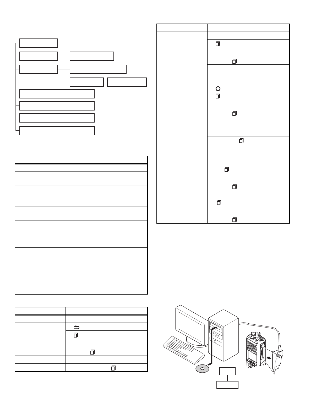
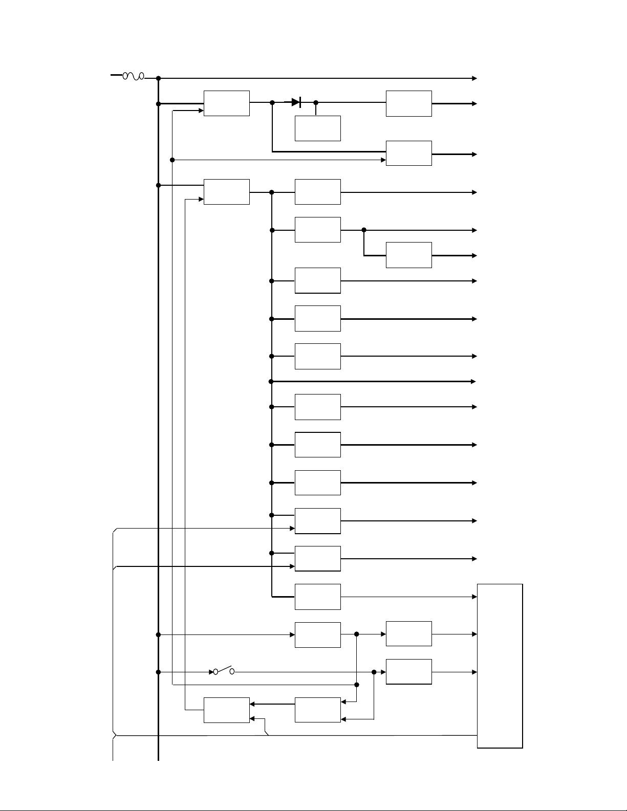
2.1 SYSTEM SET-UP
Merchandise received
Choose the type of transceiver
Transceiver programming
Are you using the speaker microphone?
A personal computer, programming interface (KPG-36U/36X),
and FPU (programming software) are required for programming.
(The frequency, and signaling data are programmed for the transceiver.)
NO
NO (Option)
YES
KMC-41/KMC-42W/
KMC-54WD
Speaker microphone
Are you using the secure cryptographic module?
NO
(Option)
YES
KWD-AE30/AE31 Refer to the "2.3.1 SECURE CRYPTOGRAPHIC
MODULE (KWD-AE30/KWD-AE31:Option)".
* If the internal GPS function
is not used, the KMC-47GPSD
can be used as GPS
speaker microphone.
Delivery
Type
DTMF keypad
RF power
No
6W NX-5200 K3 Yes
TX/RX 136~174
6W
6W
6W
No
NX-5200 F3
NX-5200 F2
Yes
NX-5200 K2
No
6W NX-5200 E2
Yes
6W NX-5200 E
Frequency range (MHz)
Are you using the optional antenna?
YES
KRA-22/KRA-26/KRA-41
Optional antenna
(Option)
SECTION 1
PRECAUTION
This service manual does not describe PRECAUTION.
SECTION 2
SPECIFIC SERVICE INSTRUCTIONS
(No.RA018<Rev.002>)1-7
2.2 REALIGNMENT
User mode
Data programming mode
PC tuning mode
Transceiver information mode
PC mode
Panel tuning mode
Panel test mode
Firmware programming mode
Clone mode
Front panel programming mode*1
PC test mode
2.2.1 Modes
*1:In order to use the Front panel programming mode, it is necessary to purchase the "Front panel program" feature option.
Mode Function
User mode For normal use.
Panel test mode Used by the dealer to check the fundamen-
tal characteristics.
Panel tuning mode Used by the dealer to tune the transceiver.
PC mode Used for communication between the
transceiver and PC.
Data programming
mode
Used to read and write frequency data and
other features to and from the transceiver.
PC test mode Used to check the transceiver using the
PC. This feature is included in the FPU.
Firmware programming mode
Used when changing the main program of
the flash memory.
Clone mode Used to transfer programming data from
one transceiver to another.
Front panel programming mode
Transceiver information mode
Frequency, signaling and features write to
the transceiver.
Used to confirm the transcerver firmware
version, SCM firmware version and SCM
Hardware version.
2.2.2 How to Enter Each Mode
Mode Operation
User mode Power ON
Panel test mode*2 • [ ] + Power ON
• [ ] + Power ON
Select the “Panel Test” using the [] /
[] key.
PC mode Received commands from PC
Press the [ ] key.
Panel tuning mode [Panel test mode] + [ ]
1-8 (No.RA018<Rev.002>)
Mode Operation
Firmware programming
mode*2
• [AUX (Orange)] + Power ON
• [ ] + Power ON
Select the “Firmware Prog” using the
[] / [] key.
Press the [ ] key.
• If Write is performed by KFL, Firmware programming mode will start
automatically.
Clone mode*2 • [ ] + Power ON
• [ ] + Power ON
Select the “Clone” using the [] / []
key.
Press the [ ] key.
Front panel programming mode*2
• Press the PF key to which Front panel programming mode is set during
the user mode.
• Press the [ ] key and enter the
Menu mode.
Select the any icon assigned the Front
panel programming mode using the
[] / [] key.
Press [ ] key.
Select the “Panel Program” using the
[] / [] key.
Press the [ ] key.
Transceiver
information mode*2
• [Side 3] + Power ON
• [ ] + Power ON
Select the “Transceiver Info” using the
[] / [] key.
Press the [ ] key.
*2 There is the two or three as how to enter.
2.2.3 Panel Test Mode
Setting method refer to ADJUSTMENT.
2.2.4 Panel Tuning Mode
Setting method refer to ADJUSTMENT.
2.2.5 PC Mode
2.2.5.1 Preface
The transceiver is programmed by using a personal computer,
programming interface (KPG-36U/36X) and FPU (programming
software).
The programming software can be used with a PC. Figure 1
shows the setup of a PC for programming.
PC
KPG-36U/36X
PC
FPU
USB
KPG-36U/36X
Transceiver
Fig.1

2.2.5.2 Connection procedure
(1) Connects the transceiver to the computer using the inter-
face cable (KPG-36U/36X).
Note:
You must install the KPG-36U/36X driver in the computer to use the USB programming interface cable (KPG36U/36X).
(2) When the POWER switch on, user mode can be entered
immediately. When PC sends command the transceiver
enter PC mode, and “PROGRAM” is displayed on the LCD.
When data transmitting from the transceiver, the red LED
lights.
When data receiving to the transceiver, the green LED
light.
Note:
The data stored in the computer must match the “Model
Name” when it is written into the flash memory.
2.2.5.3 KPG-36U/36X description (USB programming interface cable: Option)
The KPG-36U/36X is a cable which connects to a USB port on a
computer.
When using the KPG-36U/36X, install the supplied CD (with driver software) in the computer. The KPG-36U driver runs under
Windows XP, Vista, 7, 8 or 8.1.
The KPG-36X driver runs under Windows Vista, 7, 8 or 8.1.
The latest version of the USB driver is available for download
from the following URL:
http://www.kenwood.com/usb-com/
(This URL may change without notice.)
2.2.5.4 Programming software KPG-D1/D1N (Ver. 1.60 or
later) description
The FPU is the programming software for the transceiver supplied on a CD-ROM. This software runs under Windows Vista 7,
8 or 8.1 on a PC.
The data can be input to or read from the transceiver and edited
on the screen.
Note:
KPG-D1N can't be used for E, E2 types.
2.2.6 Firmware Programming Mode
2.2.6.1 Preface
Flash memory is mounted on the transceiver. This allows the
transceiver to be upgrade when new features are released in the
future. (For details on how to obtain the firmware, contact Customer Service.)
2.2.6.2 Connection procedure
Connect the transceiver to the personal computer using the programming interface (KPG-36U/36X). (Connection is same as in
the PC mode.)
2.2.6.3 Programming
(1) Start up the firmware programming software (KENWOOD
Firmware Loader). The KFL.exe exists in the KPG-D1/D1N
installed holder.
(2) Set the baud rate to "auto" or 1152000, 576000, 115200,
and 57600.
(3) Set the firmware to be upgrade by file name item.
(4) Enter the Firmware programming mode by using section
“2.2.2 How to Enter Each Mode”. Then, the yellow LED on
the transceiver light and "FIRMWARE PROG" is displayed.
(5) Check the connection between the transceiver and the per-
sonal computer, and make sure that the transceiver is in
the Program mode.
(6) Press “Write” button in the window. When the transceiver
starts to receive data, the “LOADING” display lights.
(7) If writing ends successfully, the checksum is calculated
and a result is displayed.
(8) If you want to continue programming other transceivers, re-
peat step (4) to (7).
Note:
If write is perfomed by KFL, Firmware programming
mode will start automatically even if Firmware programming is set to disable in the programming software.
2.2.6.4 Function
If you press the [ ] key while “FIRMWARE PROG” is displayed, the checksum is calculated, and a result is displayed. If
you press the [ ] key again while checksum is displayed,
“FIRMWARE PROG” is redisplayed.
2.2.7 Clone Mode
Programming data can be transferred from one transceiver to another by connecting them via their external universal connectors.
The operation is as follows.
The following data cannot be cloned.
• Tuning data
• Embedded message with password
• ESN (Electronic Serial Number) data
Key guide on the Clone/ Front Panel Programming Password input screen.
• Confirm ([ ] key): The password confirmation
• Delete ([ ] key): Delete the latest digit from the current
password number (Press and hold to delete all password
numbers)
• Select([ ] key): Determine the latest digit of the password
number.
(1) In the source transceiver, enter the clone mode by using
section “2.2.2 How to Enter Each Mode”. When the Clone/
Front Panel Programming Password is set to the transceiver, "Input Password" is displayed on the LCD.
If the password is not set, the transceiver displays "CLONE
MODE".
(2) When you enter the correct password, “CLONE MODE” is
displayed, the transceiver can be used as the cloning
source. The following describes how to enter the password.
(3)
- How to enter the password using the keypad;
If one of the keys 0 to 9 is pressed while the “Input Password” is displayed, the password number is displayed on
the LCD.
Each press of the key shifts the display in order to the
left.
When you enter the password and press [ ] or [*] key,
“CLONE MODE” displayed if the entered password is
correct. If password is incorrect, “Input Password” is redisplayed.
- How to enter password using the [] and [] keys;
If the [] / [] key is pressed while “Input Password” is
displayed, the Clone/ Front Panel Programming Password input screen is displayed.
If the [] or [] key is pressed while the clone/ Front
Panel Programming Password input screen is displayed,
the number (0 to 9) blinks on the LCD. When you press
the [ ] key, currently selected number is determined. If
you press the [ ] key after entering password in this
(No.RA018<Rev.002>)1-9
procedure, “CLONE MODE” is displayed if entered pass-
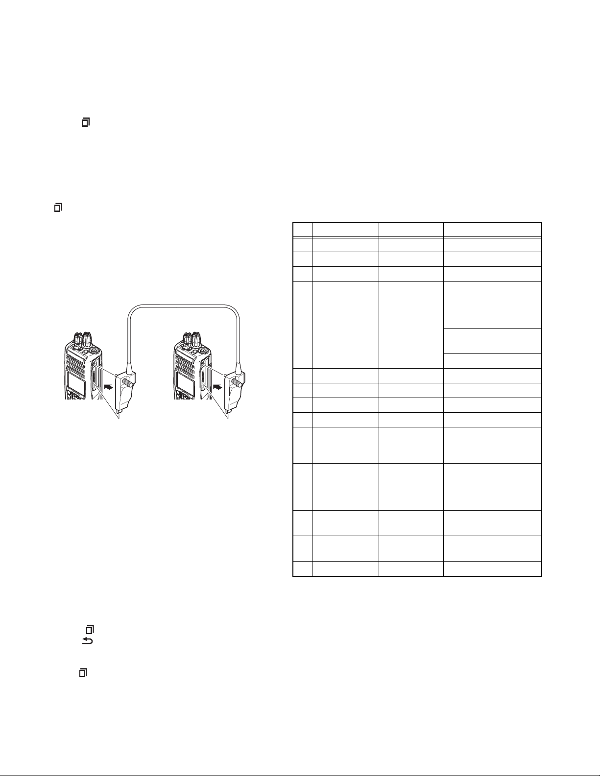
Cloning cable
(E30-3325-05)
Source
transceiver
Target
transceiver
word is correct. If the password is incorrect, “Input Password” is redisplayed.
(4) Power ON the target transceiver.
(5) Connecting the cloning cable (part No.E30-3325-05) to the
universal connectors on the source and target.
(6) Press [ ] key on the source while the source displays
“CLONE MODE”. The data of the source is sent to the target. While the target is receiving the data, “PROGRAM” is
displayed. When cloning of the data is completed, the
source displays “END”, and the target automatically operates in the User mode. The target can then be operated by
the same program as the source.
(7) The other target can be continuously cloned. When the
[ ] key on the source is pressed while the source displays
“END”, the source displays “CLONE MODE”. Carry out the
operation in step (4) to (6).
Note:
• Cannot be cloned if the password (overwrite password) is
programmed to the target.
• “Model name” must be same to clone the transceiver.
Fig.2
2.2.8 Front Panel Programming Mode
If the Front Panel Programming Mode is used, the frequency or
other data of the conventional channel is rewritable only by the
transceiver.
Moreover, the conventional channel can be added.
The following setup items can be changed or added by using the Front panel programming mode.
• RX/TX Frequency
• Channel Type
• Channel Spacing
• Decode QT/DQT/RAN/NAC, Encode QT/DQT/RAN/NAC
• Talkgroup ID List No.
• Transmit Power
• Channel Name
Key guide on the Clone/ Front Panel Programming Password input screen.
• Confirm ([ ] key): The password confirmation
• Delete ([ ] key): Delete the latest digit from the current
password number (Press and hold to delete all password
numbers)
• Select ([ ] key): Determine the latest digit of the password
number.
2.2.8.1 Enter to the Front panel programming mode.
Enter to the Menu Mode by pressing [Front Panel Mode] PF key
or [Menu] key. When the Front Panel Mode is selected, it can enter to the Front panel programming mode.
If the Clone/Front panel programming Password is not set to the
transceiver, "Panel Program" is displayed on the LCD.
If the Clone/Front panel programming Password is set to the
transceiver, "Panel Program" is displayed on the LCD when you
enter the correct password while “Input Password” is displayed.
2.2.8.2 Data Writing
Before moving to next Zone/Channel, “Keep This Change?” appears on the LCD, if you select “OK”, the new data is written to
memory. If you select “Cancel”, the new data not be written; the
new data will be erased.
• The setup items for Front panel programming mode are as
follows.
No. Setup item Display Remarks
1 RX Frequency RX Frequency Receive Frequency
2 TX Frequency TX Frequency Transmit Frequency
3 Channel Type Channel Type Analog/NXDN/P25
4 Channel
Spacing
Channel Space Analog:
12.5kHz/20kHz/25kHz
Note: 20kHz is applied
for E and E2 types only.
NXDN:
6.25kHz/12.5kHz
P25: 12.5kHz
5 RX Signaling RX QT/DQT Receive QT/DQT
6 TX Signaling TX QT/DQT Transmit QT/DQT
7 RX RAN RX RAN None, 1~63
8 TX RAN TX RAN None, 1~63
9 RX NAC RX NAC 000~FFF
(Hexadecimal)
Note: “F7F” cannot set.
10 TX NAC TX NAC 000~FFF
(Hexadecimal)
Note: “F7E” and “F7F”
cannot set.
11 Talkgroup ID
Talkgroup None, 1~1500
List Number
12 Transmit Power Transmit
Low/Medium/High
Power
13 Channel Name Channel Name
1-10 (No.RA018<Rev.002>)
• Key operation
Key\Item Zone Select Channel
Select
[ ] Decision Decision Decision Decision Decision Decision Decision Decision
[ ] Unused Back to the
previous
item
[ ] Unused Unused Unused TX Frequency
[ ] Exit panel pro-
gram mode
[] Zone change Channel
[] Zone change Channel
[] Unused Unused Frequency step
[] Unused Unused Frequency step
Keypad
[0] ~ [9]
*1
Keypad
[*] *1
Keypad
[#] *1
Zone number
select
Decision Decision Decision Decision Decision Decision Decision Decision
Unused Back to the
Exit panel
program
mode
change
change
Channel
number
select
previous
item
RX Frequency TX Frequency Channel
Type
Back to the previous item
Exit panel program mode
Fresuency up Fresuency up Channel type
Frequency
down
change
change
Go to the direct enter mode Channel
Back to the previous item
Back to the
previous item
OFF
Exit panel program mode
Frequency
down
Frequency
step change
Frequency
step change
Back to the
previous item
Back to the
previous item
Unused Unused Unused Unused
Exit panel
program
mode
change
Channel type
change
Unused Unused Signaling type
Unused Unused Signaling type
number
select (1 or 2)
Back to the
previous item
Channel
Spacing
Back to the
previous item
Exit panel
program
mode
Channel
Spacing
Change
Channel
Spacing
Change
Channel
spacing
select (1 or 2)
Back to the
previous item
RX Signaling TX Signaling
Back to the
previous item
Exit panel program mode
Signaling
number
change
Signaling
number
change
change
change
Go to the direct enter mode
Back to the
previous item
Back to the
previous item
Exit panel
program
mode
Signaling
number
change
Signaling
number
change
Signaling
type change
Signaling
type change
Back to the
previous item
Key\Item RX RAN TX RAN RX NAC TX NAC TG ID List No. Transmit
Power
[ ] Decision Decision Decision Decision Decision Decision Decision
[ ] Back to the pre-
vious item
[ ] Unused Unused Unused Unused Unused Unused Character/Digit
[ ] Exit panel pro-
gram mode
[] RX RAN up TX RAN up RX NAC up TX NAC up TG List numberupTransmit power
[] RX RAN down TX RAN down RX NAC down TX NAC down TG List number
[] RX RAN ON/
OFF
[] RX RAN ON/
OFF
Keypad
[0] ~ [9] *1
Keypad
[*] *1
Keypad
[#] *1
Go to the direct enter mode Talkgroup List
Decision Decision Decision Decision Decision Decision Decision/ Char-
Back to the
previous item
Back to the previous item
Exit panel program mode
RX RAN ON/
OFF
RX RAN ON/
OFF
Back to the
previous item
Back to the previous item
Exit panel program mode
Unused Unused Unused Unused
Unused Unused Unused Unused
Back to the
previous item
Back to the previous item
Exit panel program mode
Back to the
previous item
Back to the previous item
Exit panel program mode
down
number select
Back to the
previous item
Back to the previous item
Exit panel program mode
change
Transmit power
change
Transmit power
select (1, 2 or 3)
Back to the
previous item
Channel Name
Back to the previous item/Delete
switching
Exit panel program mode
Go to the direct
enter mode
acter/ Digit
switching
Back to the
previous item
(No.RA018<Rev.002>)1-11
• Direct enter mode
Key\Item RX
Frequency
[ ] Decision Character/Channel name decision
[ ] Delete
[ ] Unused
[ ] Exit panel program mode
[] Unused Character selection (upper case char-
[] Character selection (upper case char-
[] Move a cursor to the right
[] Move a cursor to the left
Keypad
[0] ~ [9] *1
Keypad
[*] *1
Keypad
[#] *1
*1: F3,K3,E types only
Add a digit to the current number
Decision Input character switching
Delete/Back to the previous item Delete
TX
Frequency
RX
Signaling
TX
Signaling
RX
RAN
TX
RAN
RX
NAC
TX
NAC
acter → lower-case character → digit
→ upper case character...)
acter → lower-case character → digit
→ upper case character...)
Channel
Name
1-12 (No.RA018<Rev.002>)
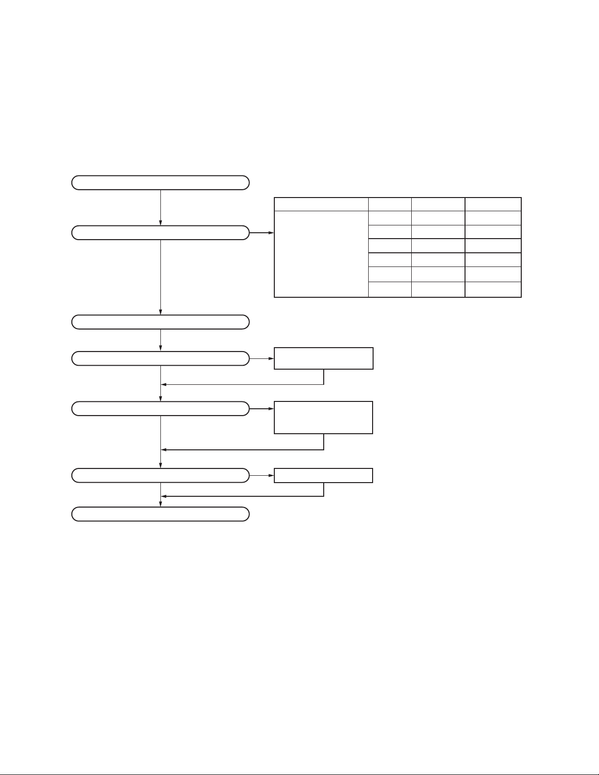
• Front panel programming mode flow chart
Enter the Front panel programming mode
by using section "2.2.2 How to Enter Each Mode".
Keep This Change?
Channel Name
Transmit Power Low Medium High
[ ] or [ ]
[ ]
[ ]
[ ] or [ ] [ ] or [ ]
Input Password
Clone/Front Panel Password
[ ]
Front panel Programming mode
Zone-Channel Format
[ ]
Zone Select
[ ]
Channel Select
[ ]
Blank Channel
[ ]
is "Personality".
Select the setting channel.
[No]
[Channel Type]: "Mixed" and
when Channel Spacing in two kinds of Channel Type is set.
[Channel Type]:
"P25","Mixed"(Transmit Mode:P25) and
when two kinds of Channel Type is set.
[Channel Type]: "NXDN",
"Mixed"(Transmit Mode:NXDN) and
when two kinds of Channel Type is set.
[ ]
[TX Frequency]: "OFF"
[Channel Type]: "Analog"
[ ]
[Channel Type]: "Analog"
[ ]
[TX Frequency]: "OFF"
[Channel Type]: "NXDN"
[ ]
[Channel Type]: "NXDN",
"Mixed"(Transmit Mode: NXDN)
[ ]
[TX Frequency]: "OFF"
[Channel Type]: "P25"
[ ]
Talkgroup List ID Amount: 0
[ ]
Note:
Zone-Channel Format allows you to whether to configure for
each zone the channels in the same system, or channels in different system.
P25 can be configured for System Select or Channel Type if one or
more P25 conventional system is preconfigured by the FPU.
"System Type = Conventional"
there is more than two.
System Select
[ ]
RX Frfequency
[ ]
[ ]
Channel Type Analog
[ ]
Transmit Mode select
Channel Spacing
[ ]
[Channel Type]: "Analog","Mixed"(Transmit Mode: NXDN),
"Mixed"(Transmit Mode: P25) and when a kind of Channel Type is set.
RX Signaling
[ ]
[TX Frequency]: Other than "OFF"
[Channel Type]: "Analog","Mixed"(Transmit Mode: NXDN),"Mixed"(Transmit Mode: P25)
TX Signaling
RX RAN
[ ]
[TX Frequency]: Other than "OFF"
[Channel Type]: "NXDN","Mixed"(Transmit Mode: NXDN)
TX RAN
RX NAC
[ ]
[TX Frequency]: Other than "OFF"
[Channel Type]: "P25","Mixed"(Transmit Mode: P25)
TX NAC
[ ]
[Channel Type]: "P25","Mixed"(Transmit Mode: P25)
Talkgroup ID List Amount must not be 0.
Talkgroup ID List Number
[No]
[ ] or [ ][ ] or [ ]
Analog P25 NXDN
[ ]
[Channel Type]: "Analog","Mixed"(Transmit Mode: NXDN),"Mixed"(Transmit Mode: P25)
OFFTX Frequency
[ ] or [ ]
Analog
[ ] or [ ]
12.5kHz
[ ] or [ ] [ ] or [ ] [ ] or [ ]
OFF QT DQT N DQT I
[ ] or [ ] [ ] or [ ] [ ] or [ ]
OFF QT DQT N DQT I
[System Type]: "P25" or ”NXDN” and [Channel Type]: "Mixed"
Mixed
[ ] or [ ]
[ ] or [ ]
[ ] or [ ]
[ ] or [ ]
[ ] or [ ]
[System Type]: "P25"
P25
[System Type]: "NXDN"
NXDN
[System Type]: "P25"
P25
[System Type]: "NXDN"
NXDN
[ ] or [ ]
12.5kHz 25.0kHz 20.0kHz
When the KPG-D1N is used, 25.0kHz may not be allowed
depends on the frequency (F2, F3, K2, K3 types only).
[Channel Type]: "NXDN","Mixed"(Transmit Mode: NXDN)
[ ] or [ ]
6.25Hz
(No.RA018<Rev.002>)1-13
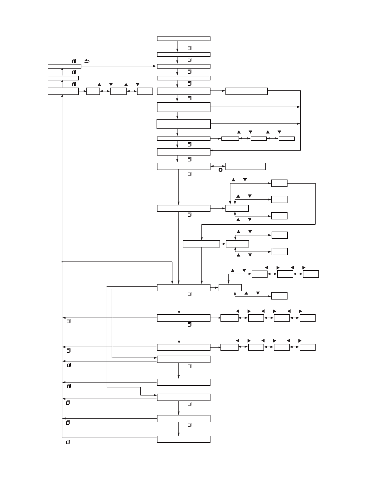
2.2.9 Transceiver Information Mode
Orange rubber seal
Cover
A
r
Use this function to confirm the transceiver firmware version, SCM Firmware version and SCM Hardware version.
(1) Enter the Transceiver Information mode by using section "2.2.2 How to Enter Each Mode".
(2) The transceiver fi rmware version appears on the LCD.
(3) Use the [] and [] keys to select the confirmation items.
㪫㫉㪸㫅㫊㪺㪼㫀㫍㪼㫉㩷
㪽㫀㫉㫄㫎㪸㫉㪼㩷㫍㪼㫉㫊㫀㫆㫅
[ ]/[ ] [ ]/[ ]
㪪㪚㪤㩷㪝㫀㫉㫄㫎㪸㫉㪼㩷
㫍㪼㫉㫊㫀㫆㫅
[ ]/[ ]
(4) To exit the transceiver information mode, turn the transceiver power OFF.
Note:
When the SCM board is not equipped to the transceiver, SCM Firmware Version and SCM Hardware Version are displayed
as "-.-.-.".
2.3 INSTALLATION
2.3.1 SECURE CRYPTOGRAPHIC MODULE (KWD-AE30/KWD-AE31:Option)
2.3.2 SUPPLIED ACCESSORIES
Connecting cable *
(X42-3330-XX)
Cushion A *
(G13-2179-XX)
Cushion B *
(G13-2178-XX)
Note:
Supplied accessories with * mark are not used for the NX-5200.
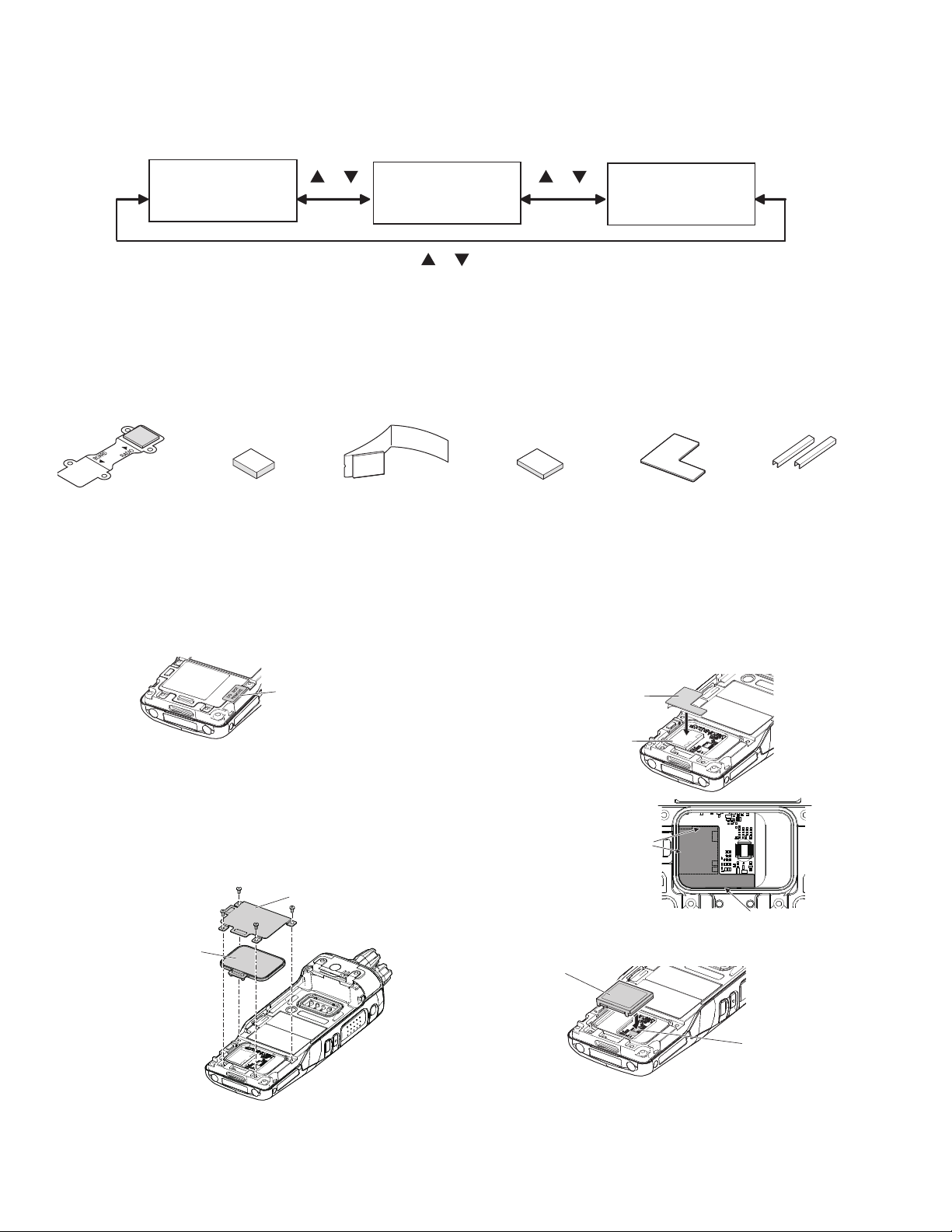
2.3.3 INSTALLING THE MODULE IN THE TRANSCEIVER
ATTENTION:
When installing the module, please take measures to prevent static electricity.
(1) Remove the VOID sheet.
Cushion C *
(G1D-0006-XX)
(4) Remove the release paper from one side of cushion D,
then attach the cushion to the shielding case of the module.
㪪㪚㪤㩷㪟㪸㫉㪻㫎㪸㫉㪼㩷
㫍㪼㫉㫊㫀㫆㫅
Cushion D
(G1D-0055-XX)
Spacer
(F3K-0004-XX)
CAUTION:
Regarding VOID, confirm the service policy of the NX5200 to KENWOOD (or authorized distributor). In addition, when installing the module, remove VOID sheet af-
ter understanding the service policy.
(2) Remove the 4 screws from the cover.
(3) Remove the cover and orange rubber seal from the trans-
ceiver.
VOID sheet
Cushion D
Shielding case
ttach the cushion
correctly to the position of
the chassis and shielding
case (end-face).
Insert the cushion under the chassis.
(5) Insert the module to the connector of the PCB.
Module
Connecto
1-14 (No.RA018<Rev.002>)
(6) Attach two spacers to the back side of the orange rubber
seal as indicated below.
Note:
• When the KWD-AE30/ KWD-AE31 is installed, select the
"Secure Cryptographic Module" checkbox in the Product Information of the KPG-D1/KPG-D1N (programming soft-
Spacer
ware), and then set each parameter.
• If the KWD-AE30/ KWD-AE31 connector is not properly installed, the TX/RX indicator will blink red or "No SCM" will
Note:
Rubber seal may not attach correctly if the spacer is
brought near by the corner too much.
(7) Reinstall the cover and orange rubber seal using the 4
screws removed in step 2 and 3.
Note:
When installing the rubber orange seal on the chassis,
appear on the display when the transceiver power is turned
on.
• If the Encryption Key data is not written at the Keyloader, or
the Encryption Key data is zeroized, "Key Fail" will appear
on the display.
• If the KWD-AE30/ KWD-AE31 is installed in other transceivers, the Encryption Key data will be forced to zeroize.
ensure that you do not damage the rubber seal and that
the contact area of the chassis is dust-free.
2.4 CIRCUIT DESCRIPTION
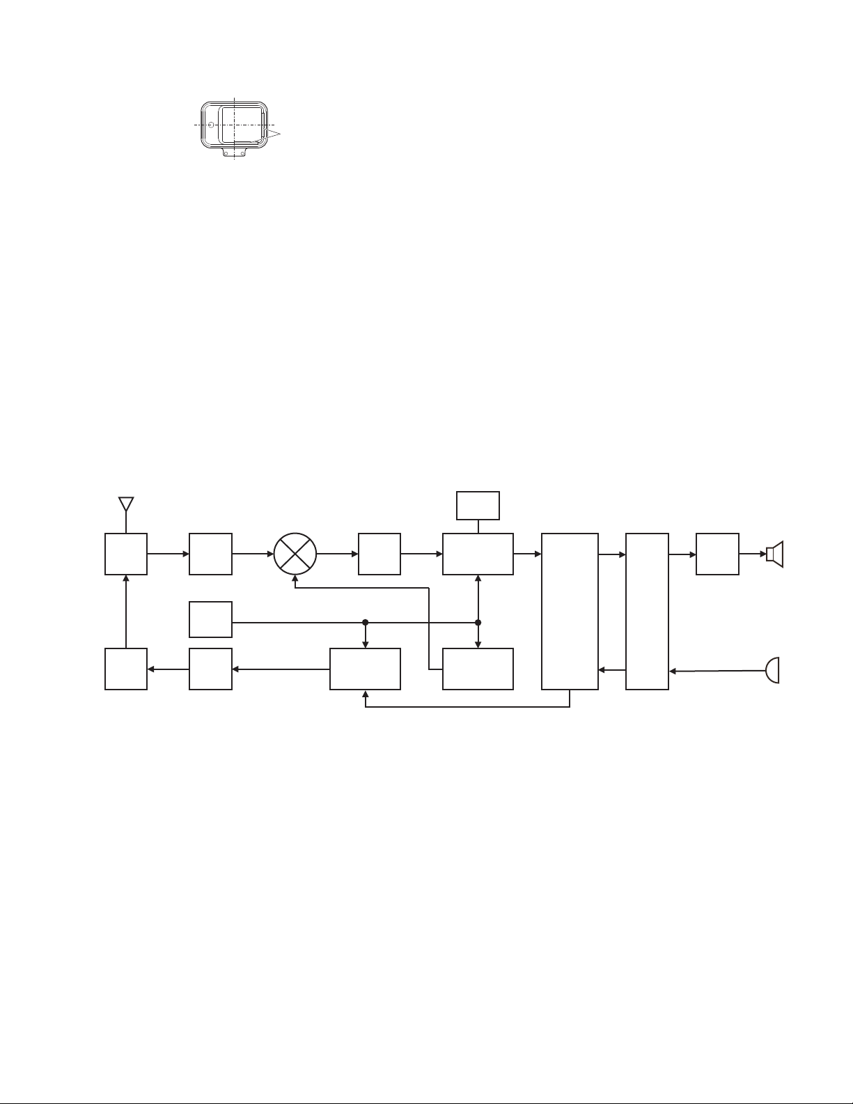
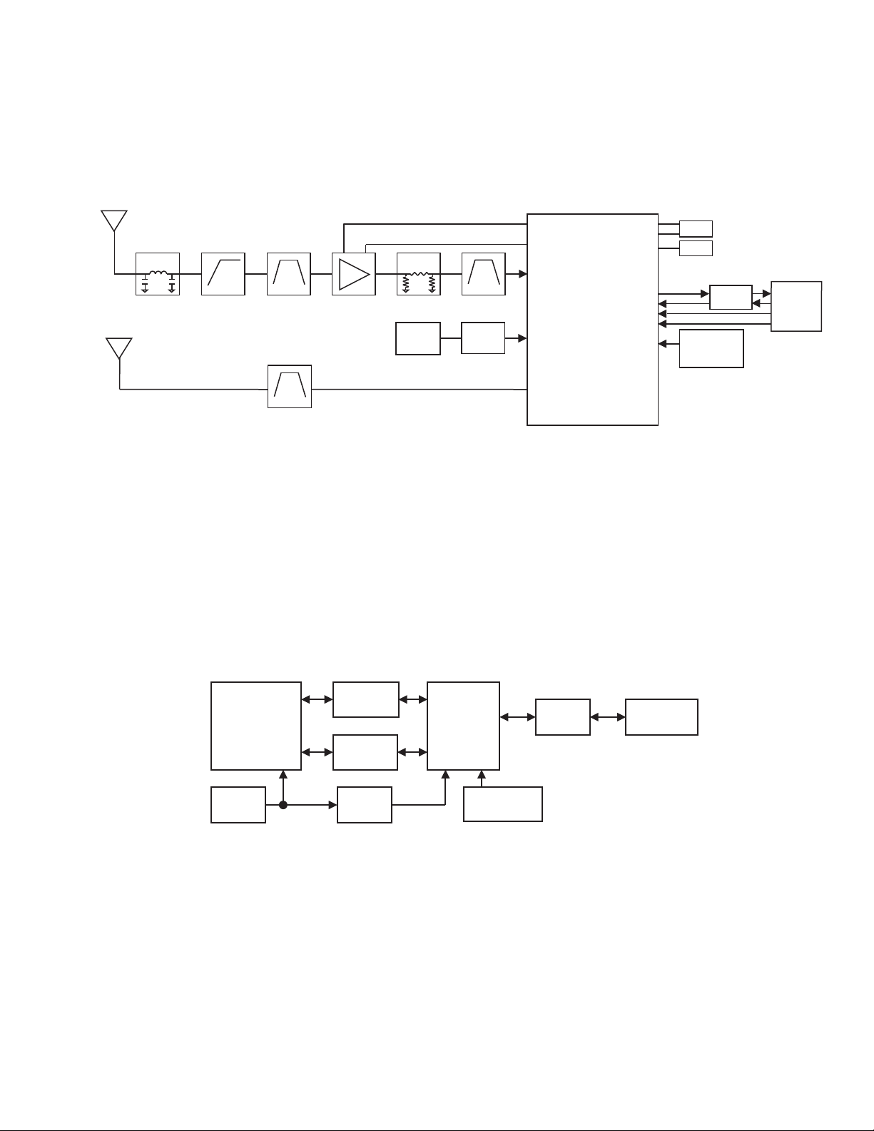
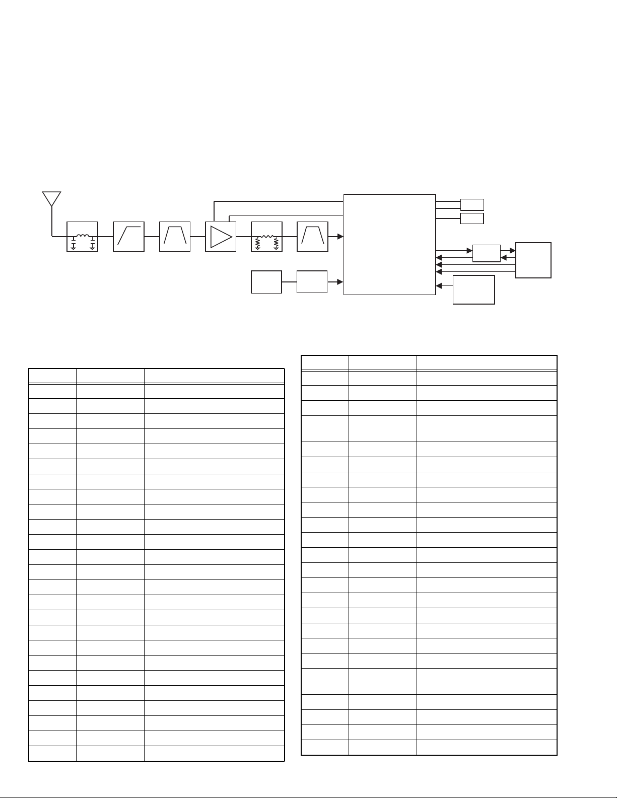
2.4.1 Overview
The NX-5200 is a VHF Analog FM & Digital Portable transceiver designed to operate in the frequency range of 136 to 174MHz.
The unit consists of a receiver, a transmitter, a phase-locked loop (PLL) frequency synthesizer, a digital control unit, and a power supply circuit.
2.4.2 Frequency Configuration
The receiver is a double-conversion super-heterodyne using a first intermediate frequency (IF) of 49.95MHz and second IF of
2.25MHz. Incoming signals from the antenna are mixed with the local signal from the PLL circuit to produce the first IF of 49.95MHz.
This is then mixed with the 47.7MHz second local oscillator output to produce the 2.25MHz second IF. The transmit signal frequency
is generated by the PLL VCO, and modulated by the signal from the DSP. It is then amplified and fed to the antenna.
ANT
TX/RX: 136~174MHz
ANT
SW
RF
AMP
1st MIX 49.95MHz 47.7MHz
MCF
2nd
VCO
MIX
IF Circuit
SP
AF
AMP
185.95~223.95MHz
TX PLL
VCO
RX PLL
VCO
Baseband
Circuit
CODEC
MIC
PA
AMP
19.2MHz
TCXO
TX
AMP
136~174MHz
Fig.1 Frequency configuration
2.4.3 Receiver System
2.4.3.1 RF Circuit
The receive signal from antenna switch (D350, D351, D370 and D371) is amplified by a RF amplifier (Q530) and passes through the
band-pass filter (L530, L535, L520 and L532) to remove unwanted signals. The signal is then fed to the 1st mixer (Q500).
2.4.3.2 IF Circuit
The first IF signal is passed through a four-pole monolithic crystal filter (XF670) to reject adjacent channel signals. The filtered first IF
signal is amplified by the first IF amplifier (Q670 and Q660) and then applied to the IF system IC (IC600). The IF system IC provides
a second mixer, second PLL, AGC and A/D converter.
The second mixer mixes the first IF signal with the 47.7MHz of second local oscillator output and produces the second IF signal of
2.25MHz.
The second IF signal is then be fed into an A/D converter, generates the I and Q data. This data is in the form of SSI (Serial Synchronous Interface), and sent to the DSP (IC702).
(No.RA018<Rev.002>)1-15
2.4.3.3 Audio Amplifier Circuit
A
Audio processing (high-pass filter, low-pass filter, de-emphasized and so on) at Analog FM mode and decoding at Digital mode are
processed by DSP. SSI signal from DSP is converted to audio signal at IC902. The signal goes to amplifier (IC904 or IC905).
While INTAMT is High, IC904 is activated and audio is heard from internal speaker.
While EXTAMT is High, IC905 is activated and audio is heard from external speaker.
NT
LPF
D350, D351
D370, D371
ANT
SW
L535
L530
BPF
Q530
RF AMP
L520
L532
BPF
Q500 XF670 Q670
BPF IF IC
MCF IF AMP IF AMP IC600
RX PLL
Q660
2nd
VCO
Q600
SSI
DSP CODEC
IC702 IC902
INTAMT
EXTAMT
IC904
IC905
Internal Speaker
External Speaker
Fig.2 RF and IF circuit
2.4.4 Transmitter System
2.4.4.1 Audio Band Circuit
The signal from microphone is amplified and converted to digital signal by IC902. IC902 includes AGC function.
Digital signal is transferred to IC702 through SSI.
2.4.4.2 Baseband Circuit
The audio signal transferred from IC902 is processed at IC702. Voice signals of 300Hz or lower and frequencies of 3kHz or higher are
cut off and an audio range 300Hz to 3kHz is extracted. The audio signal is then pre-emphasized in FM mode and synthesized with
the signals, such as QT and DQT, as required, and is transferred to PLL Frequency Synthesizer block. The DTMF and MSK baseband
signals are also generated by IC702.
In Digital mode, the audio signal is converted to the 4-Level FSK baseband signal and is transferred to PLL Frequency Synthesizer
block.
The output level according to the transmit carrier is fine-adjusted according to each modulation method.
2.4.4.3 Drive and Final Amplifier
The signal from the TX PLL is amplified by pre-drive amplifier (IC300 and Q310). The output of the pre-drive amplifier is amplified by
the drive amplifier (Q320) and final amplifier (Q330) to 6W (1W when the power is low). IC300 is MMIC. Q310, Q320 and Q330 are
MOS FET. The output of the final amplifier is then passed through the harmonic filter (LPF) and antenna switch (D350, D351, D370
and D371) and applied to the antenna terminal.
2.4.4.4 APC Circuit
The APC circuit always monitors the current flowing through the drive amplifier (Q320) and final amplifier (Q330). The APC keeps a
current constant.
The voltage drop at R400 and R402 is caused by the current flowing through the RF power amplifier and this voltage is applied to APC
circuit. Output voltage from APC controls the VGG of Q310, Q320 and Q330 to keep the current constant. The change of power high/
low is carried out by the change of the reference voltage.
TX PLL
IC300 Q310 Q320
PreDrive 1
PreDrive 2
Drive Final
Q330
ANT
SW
R400
R402
+B APC reference voltage
APC
IC400
Fig.3 Drive and Final amplifier and APC circuit
1-16 (No.RA018<Rev.002>)

2.4.5 PLL Frequency Synthesizer
2.4.5.1 TCXO (X700)
TCXO (X700) generates a reference frequency of 19.2MHz for the PLL frequency synthesizer. This reference signal is buffered by
Q700 and IC700. And it is distributed to TX PLL (IC100), RX PLL (IC200), IF IC (IC600), GPS/Bluetooth (IC850), and IC702.
The frequency adjustment is achieved by adjusting a D/A converter (IC901) output in the voltage of the control terminal of TCXO.
2.4.5.2 VCO
There are TX VCO and RX VCO.
The TX VCO (Q160) generates the carrier for the transmitter. The VCO oscillation frequency range is 136 to 174MHz. The transmit
frequency range is 136 to 174MHz.
The RX VCO (Q240) generates the 1st local signal for the receiver.
The VCO oscillation frequency range is 185.95 to 223.95MHz. The 1st local signal frequency range is 185.95 to 223.95MHz.
The VCO oscillation frequency is determined by voltage control terminals "CV" and "ASSIST". The voltage control terminal "CV" is
controlled by PLL IC (IC100 for TX PLL, IC200 for RX PLL). The voltage control terminal "ASSIST" is controlled by the control voltage
from D/A converter (IC901).
For the modulation input terminal, "VCO_MOD" of TX VCO (Q160), the output frequency changes according to the applied voltage.
This is used to modulate the VCO output.
2.4.5.3 PLL IC
There are TX PLL IC and RX PLL IC. PLL ICs compare the difference in phases of the VCO oscillation signal and the TCXO reference
frequency. And it returns the difference voltage to the VCO CV terminal and realizes the "Phase Locked Loop". This allows the VCO
oscillation frequency to accurately match (lock) the desired frequency.
When the frequency is controlled by the PLL, the frequency convergence time increases as the frequency difference increases when
the set frequency is changed. To supplement this, the MPU is used before control by the PLL IC to bring the VCO oscillation frequency
close to the desired frequency. As a result, the VCO CV voltage does not change and is always stable at approx. 2.0V.
The desired frequency is set for the PLL IC by the MPU (IC702) through the 3-line "SDO1", "SCK1", "/PCS_R" serial bus for RX PLL
and "SDO1", "SCK1", "/PCS_T" serial bus for TX PLL. The MPU monitors through the "PLD_R" and "PLD_T" signal line, whether the
PLL IC is locked or not. If the VCO does not lock to desired frequency (unlock), the "PLD_R" and "PLD_T" logic is low.
2.4.6 Control Circuit
The control circuit consists of MPU/DSP (IC702) and its peripheral circuits. IC702 mainly performs the following;
(1) Switching between transmission and reception by PTT signal input.
(2) Reading system, zone, frequency, and program data from the memory circuit.
(3) Sending frequency program data to the PLL.
(4) Controlling the audio mute circuit by decode data input.
2.4.6.1 MPU
The MPU/DSP (IC702) is 32-bit RISC processor and fixed floating-point VLIW DSP, equipped with peripheral function.
This MPU operates at 288MHz (MAX) clock and 3.3V /1.8V/ 1.2V DC. Controls the flash memory, Mobile DDR, the receive circuit, the
transmitter circuit, the control circuit, and the display circuit and transfers data to or from an external device.
2.4.6.2 Memory Circuit
Memory circuit consists of the MPU (IC702) and the Mobile DDR (IC703), the flash memory (IC705). The flash memory has capacity
of 512M-bit that contains the transceiver control program for the MPU and stores the data. It also stores the data for transceiver channels and operating parameter that are written by the FPU. This program can be easily written from external devices. The Mobile DDR
has capacity of 512 M-bit. The MPU copies the program to the Mobile DDR from the flash memory. The MPU is used as a work area
Mobile DDR.
Flash Memory
Note:
The flash memory stores the data that is written by the FPU (KPG-D1/D1N), tuning data (Deviation, Squelch, etc.), and firmware
program (User mode, Test mode, Tuning mode, etc.). This data must be rewritten when replacing the flash memory.
Mobile DDR (static memory)
Note:
Mobile DDR is used as a work area of the MPU.
2.4.6.3 LCD
The LCD is controlled using parallel interface from the MPU (IC702).
2.4.6.4 Key Detection Circuit
Keys are detected using I/O Expander IC (IC708). If pressed key is detected by IC708, it is informed to the MPU (IC702) through serial
line.
(No.RA018<Rev.002>)1-17

2.4.6.5 Low Battery Warning
The battery voltage is divided using R40 and R41 and is detected by A/D converter (IC900). When the battery voltage falls below the
voltage set by the Low battery warning adjustment, the red LED blinks to notify the operator that it is time to replace the battery. If the
battery voltage falls even more (approx. 5.8V), a beep sounds and transmission stops.
Low battery warning Battery condition
The red LED blinks during transmission. The battery voltage is low but the transceiv-
er is still usable.
The red LED blinks and the warning tone
beeps while the PTT switch is pressed.
2.4.6.6 DSP
The DSP circuit consists of a MPU/DSP (IC702) and processes the baseband signal. The DSP operates at 288MHz (MAX) clock, the
I/O section operates at 3.3V/1.8V and the core section operates at 1.2V.
The DSP carries out the following processes:
• 4 Level FSK processing
• Analog FM pre-emphasis/de-emphasis
• Vocoder processing between audio codec and modulation/demodulation
• CAI processing, such as error correction encoding
• QT/DQT encoding/decoding
• DTMF encoding/decoding
• MSK encoding/decoding
• 2-tone encoding/decoding
• Compressor/expander processing
• Voice scrambler processing
• Transmit/receive audio filtering processing
• Microphone amplifier AGC processing
• Audio mute processing
• Modulation level processing
• Active Noise Reduction
• Voice recording/playback processing
• Voice announce processing
The battery voltage is low and the transceiver is not usable to make calls.
2.4.7 Power Supply Circuit
The battery voltage (+B) is provided from battery terminal. The battery voltage passes through the 3.15A fuse (F1), and goes to RF
final amplifier, AVR ICs (IC31, IC82, IC801, IC36, IC63, IC65, IC64), DC/DC converter (IC33), transistor (Q32, Q71 through the 1A
fuse (F2)), and voltage detector IC (IC20). Voltage detector (IC20) watches battery voltage. If the battery voltage is enough higher
than 5.6V, detector outputs High. Then, IC31 (31BU) outputs 3.1V, and IC32 (12BU) outputs 1.2V, and Q31 is turned on.
When the VOL SW is turned on, SB1 becomes high (battery voltage). The DC/DC (IC33) operates if both SB1 and output of detector
are high. IC33 (38M) outputs 3.8V, and A30 (12M) outputs 1.2V. Then, IC34 (18M) and IC37 (18BT) outputs 1.8V. Then, IC80 (30M)
outputs 3.0V, and IC38 (33BT) and IC35 (33M) and IC81 (33OPT) outputs 3.3V. Then, IC39 (33A) outputs 3.3V, and IC82 (50A) outputs 5.0V. Then, IC701 (18M_3) outputs 1.8V, and Q71 (53AF) is turned on. Voltage detector (IC704) watches IC33 (38M) output
voltage. If the 38M output voltage is enough higher than 3.5V, detector outputs High. As a result, the MPU/DSP operate.
The SBC signal becomes High after the MPU/DSP operates, and IC61 (33C), IC36 (50C), IC63 (50VCO) and Q32 (SB2) are turned on.
When SD_EN signal becomes High, IC30 (33SD) operates. When 5UC signal becomes High, IC801 (50U) operates. When TXC signal
becomes High, IC65 (50T) operates. IC65 (50T) is turned on in transmit mode.
When RXC signal becomes High, IC64 (50R) operates. IC64 (50R) is turned on in receive mode. Switches are controlled by the MPU/
DSP.
When the VOL SW is turned off /PSW signal becomes Low. After detecting /PSW signal, the MPU/DSP changes SBC signal to Low.
The 50C is fed to IC60 (130C). IC60 (130C) is the DC/DC boost converter. IC60, D60, C64 consist of a DC/DC boost converter. The
130C circuit then outputs approximately +13VDC.
1-18 (No.RA018<Rev.002>)
Battery
F1
(3.15A)
+B
Final Amp, APC, Drive Amp
IC31
31BU
IC33
38M
BackUp
Battery
A30
12M
IC34
18M
IC37
18BT
IC38
33BT
IC80
30M
IC32
12BU
Q31
SW
IC701
18M_3
MPU/DSP RTC
SCM Board
MPU/DSP Core,
MPU/DSP PLL
MPU/DSP 1.8V I/O, mDDR2,
LCD Module I/O
Flash ROM I/O,
AudioCodec DVDD
BT & GPS I/O
BT & GPS VDD
LCD Module
LCD BackLight
SD_EN
SBC
VOL SW
IC39
33A
IC35
33M
IC81
33OPT
IC30
33SD
IC61
33C
IC704
3.5V DET
IC20
5.6V DET
Q22
Lvl Conv
Q21
Lvl Conv
/RST
/BINT
/PSWSB1
AudioCodec VDD,
8bit/8ch DAC, 12bit/4ch DAC
MPU/DSP 3.3V I/O,
Flash ROM VCC,
AudioCodec IOVDD
SCM Board
microSD
PLL, IF
IC702
MPU/DSP
D20
OR
Q20
AND
SBC
(No.RA018<Rev.002>)1-19
IC82
50A
KEY Back Light, 3Color LED,
8bit/16ch ADC, Universal I/F
5UC
SBC
ANTSW
SBC
TX
RX
TXC
RXC
SBC
F2
(1A)
IC801
50U
IC36
50C
IC63
50VCO
IC65
50T
IC64
50R
Q32
SB2
Q71
53AF
IC60
130C
IC360
SW
Q110
SW
Q210
SW
Universal Option
PLL, IF, VCO
ASSIST
ANTSW
TX VCO
RX VCO
TX circuit
RX circuit
8bit ADC
Int AF Amp
Ext AF Amp
Fig.4 Power supply circuit
2.4.8 Signaling Circuit
2.4.8.1 Encode (QT/DQT/DTMF/2-tone/MSK)
Each signaling data signal of QT, DQT, DTMF, 2-tone and MSK is generated by IC702, superposed on a modulation signal and is sent
to TX VCO and TX PLL IC.
2.4.8.2 Decode (QT/DQT/DTMF/2-tone/MSK)
The audio signal is removed from the FM detection signal sent to the IC702 and the resulting signal is decoded by IC702.
1-20 (No.RA018<Rev.002>)
2.4.9 Bluetooth/GPS Circuit
The main component of the BT/GPS circuit is BT/GPS IC (IC850).
The clocks of BT/GPS IC require 19.2MHz for core and 32.768kHz slow clock (X850) for UART.
19.2MHz clock (X700) is shared with MPU/DSP (IC702), and is supplied through the clock buffer IC (IC700).
The BT/GPS IC communicates to the MPU/DSP (IC702) on the HCI UART. Interface of UART & Digital audio (PCM) between the
MPU/DSP (IC702) and the BT/GPS IC (IC850), have level conversion at the level conversion IC (IC852, IC853).
The BT/GPS IC is powered by 1.8V and 3.3V which are supplied from two discrete external regulators (IC38 and IC37). The input of
these regulators is sourced from a switching regulator (IC33) which regulates the battery voltage to 3.8V.
GPS antenna
BT antenna
Matching
HPF
Pre-SAW Post-SAWLNA
LC filter
LNA Supply
LNA Enable
Attenuat or
TCXO
19.2MHz
IC700
Clock
Buffer
IC850 BT/GPS IC
VDD_TCXO(G1)
GPS_EXT_LNA_EN(H6)
GPS IC(IC850)
GPS_LNA_IN(L2)
BT_HCI_UART_TX(A4)
BT_HCI_UART_RX(B5)
BTFM_nSHUTDOWN(A6)
TCXO_CLK_LV(F1)
BT_RF
VBAT1(A2)
TCXO_LDO_IN(H1)
GPS PA EN(G3)
RTC_CLK(H9)
VDDS
3.3V
1.8V
GPS_TX
GPS_RX
OSCILLATOR
32.768kHz
Level
Conversion
IC702
MPU/DSP
Fig.5 Bluetooth/GPS circuit
2.4.9.1 Bluetooth Circuit
The BT/GPS IC (IC850) support Bluetooth 3.0 up to HCI level.
The TX/RX frequency is 2400-2483.5MHz (79ch Hopping, 2402-2480MHz, 1MHz step). The transmit power is +2dBm at Bluetooth
antenna input.
The Bluetooth antenna is made of sheet metal, and connected to the BT/GPS IC (IC850) through the LC filter (L855).
Frequency configuration for Bluetooth is following:
There are two LO modes: 2X and Offset LO (OSLO). 2X where LO is 2*RF_FREQ (e.g. when transmitting at 2441MHz it is at
4882MHz). OSLO where LO is at 2/3*RF_FREQ (e.g. when transmitting at 2441MHz it is at 1627.333MHz).
In RX the 2X is always used.
In GFSK TX if power is 10dBm or more then OSLO is used.
In EDR2 TX if power is -12dBm or more then OSLO is used.
In EDR3 TX if power is -12dBm or more then OSLO is used.
Otherwise 2X is used for TX as well.
IC702 IC852 IC850
UART UART
MPU/DSP
PCM
Level
Conversion
IC853
Level
PCM
BT/GPS
IC
L855
LC
Filter
Bluetooth
Anttena
Sheet metal
Conversion
X700 IC700 X850
TCXO
19.2MH
Clock
Buffer
32.768kHz
Clock
Fig.6 Bluetooth circuit
(No.RA018<Rev.002>)1-21
2.4.9.2 GPS Circuit
1.8V
3.3V
OSCILLATOR
32.768kHz
GPS_TX
GPS_RX
IC702
IC850 BT/GPS IC
IC700
MPU/DSP
HPF
Pre-SAW LNAMatching
GPS antenna
Post-SAWAttenuator
LNA Supply
LNA Enable
TCXO
19.2MHz
Clock
Buffer
Level
Conversion
GPS IC(IC850)
GPS_LNA_IN(L2)
GPS_EXT_LNA_EN(H6)
VDD_TCXO(G1)
TCXO_CLK_LV(F1)
BT_HCI_UART_TX(A4)
BT_HCI_UART_RX(B5)
RTC_CLK(H9)
BTFM_nSHUTDOWN(A6)
GPS PA EN(G3)
VBAT1(A2)
TCXO_LDO_IN(H1)
VDDS
The RF signal is received by the antenna matched by the matching circuit. The matching circuit consists of L905, C948 and C883.
And this signal applied to a high-pass filter. The filter consists of C882, C881, C880, L859 and L858. The filtered RF signal is then
applied to a SAW filter (L857).
The output of the SAW filter is fed into the LNA (IC851). The LNA is enabled by GPS_EXT_LNA_EN (pin H6 of the BT/GPS IC, IC850).
The LNA input match comprises of C879, C878 and L856. The LNA output match comprises of C874. And through the Attenuator
comprised of R857, R856 and R855, the RF signal is further filtered by a second SAW filter (L853).
The output of the second SAW filter is passed to pin L2 of the BT/GPS IC. The input match for pin L2 comprises of C867, C866 and
L852. The control and data lines for the BT/GPS IC are GPS_PA_EN, BTFM_nSHUTDOWN, GPS_TX and GPS_RX. GPS_TX and
GPS_RX are shared with the Bluetooth data line.
Frequency configuration for GPS is following:
Lo is GPS: 1571.324MHz
Fig.7 GPS circuit
2.5 COMPONENTS DESCRIPTION
2.5.1 Main unit (XC1-0331-80, XC1-0360-10)
Ref. No. Part Name Description
IC20 IC Reset
IC30 IC Voltage regulator (33SD)
IC31 IC Voltage regulator (31BU)
IC32 IC Voltage regulator (12BU)
IC33 IC DC/DC converter (38M)
IC34 IC DC/DC converter (18M)
IC35 IC Voltage regulator (33M)
IC36 IC Voltage regulator (50C)
IC37 IC Voltage regulator (18BT)
IC38 IC Voltage regulator (33BT)
IC39 IC Voltage regulator (33A)
IC60 IC DC/DC converter (130C)
IC61 IC Voltage regulator (33C)
IC63 IC Voltage regulator (50VCO)
IC64 IC Voltage regulator (50R)
IC65 IC Voltage regulator (50T)
IC70 IC Voltage regulator (53AF)
IC80 IC Voltage regulator (30M)
IC81 IC Voltage regulator (33OPT)
IC82 IC Voltage regulator (50A)
IC100 IC PLL IC
IC101 IC DC AMP
IC102 IC Voltage regulator (DC AMP)
IC200 IC PLL IC
IC201 IC DC AMP
1-22 (No.RA018<Rev.002>)
Ref. No. Part Name Description
IC300 IC Pre-drive AMP 1
IC360 IC DC SW (Antenna SW)
IC400 IC APC
IC550,
IC DC AMP
551
IC600 IC IF IC
IC700 IC Clock buffer
IC701 IC DC SW (18M)
IC702 IC MPU
IC703 IC SDRAM
IC704 IC Reset
IC705 IC Flash memory
IC706 IC Logic control
IC708 IC I/O control
IC709 IC Motion sensor
IC711,712 IC Logic control
IC800 IC LED driver
IC801 IC Voltage regulator (50U)
IC802 IC Analog SW
IC803 IC Level converter
IC804~
807
IC850 IC GPS/Bluetooth
IC851 IC GPS LNA
IC852,853 IC Level converter
IC900 IC A/D converter
IC Logic control
Ref. No. Part Name Description
IC901 IC D/A converter
IC902 IC CODEC
IC903 IC D/A converter
IC904,905 IC Audio AMP
IC906 IC Logic control
Q20 Transistor DC SW
Q21,22 FET DC SW
Q30 FET DC SW
Q31 Transistor DC SW
Q32,33 FET DC SW
Q70 Transistor DC SW
Q71 Transistor Voltage regulator (53AF)
Q100 FET DC SW
Q101 Transistor Ripple filter
Q110,111 FET DC SW
Q160 FET VCO oscillation
Q180,181 Transistor Buffer AMP
Q200 FET DC SW
Q201 Transistor Ripple filter
Q210,211 FET DC SW
Q240 FET VCO oscillation
Q280,281 Transistor Buffer AMP
Q310 FET Pre-drive AMP 2
Q320 FET Drive AMP
Q330 FET Final AMP
Q390 Transistor DC SW
Q400 Transistor DC SW
Q401,402 FET DC SW
Q403 Transistor DC SW
Q404 FET DC SW
Q500 FET Mixer
Q530 FET LNA
Q580 Transistor Buffer AMP
Q600 FET VCO oscillation
Q601 Transistor DC SW
Q602 Transistor Ripple filter
Q660 Transistor IF AMP
Q670 FET IF AMP
Q700 Transistor Buffer AMP
Q701 FET DC SW
Q702 Transistor DC SW
Q703 FET DC SW
Q800 FET DC SW
Q801 Transistor DC SW
Q850 FET DC SW
D1 Diode Reverse connection prevention
Ref. No. Part Name Description
D2 Diode Overvoltage protection
D20 Diode DC SW
D30 Diode Backup battery charge
D60 Diode DC/DC converter
D100 Zener diode Overvoltage protection
D101 Diode Ripple filter
D160~164 Variable capac-
itance diode
D200 Zener diode Overvoltage protection
D201 Diode Ripple filter
D240~243 Variable capac-
itance diode
D350,351 Diode Antenna SW
D370,371 Diode Antenna SW
D390 Zener diode Voltage limiter
D520,521 Variable capac-
itance diode
D530,531 Variable capac-
itance diode
D600,601 Variable capac-
itance diode
D603 Diode Overvoltage protection
D700 Diode Overvoltage protection
D701,702 Diode Port protection
D703 Diode Overvoltage protection
D704 LED LED
D705 Diode Reverse current prevention
D800,801 Diode Port protection
D802~804 Diode Reverse current prevention
D805,806 Zener diode Surge protection
D807 Diode DC SW
D808 Zener diode Surge protection
D809,810 Varistor Surge protection
D850,851 Diode Overvoltage protection
D900,901 Zener diode Surge protection
D902 Diode Reverse current prevention
D903 Diode DC SW
D904 Diode Reverse current prevention
D905 Diode Overvoltage protection
D906 Diode Reverse current prevention
D907 Diode Overvoltage protection
VCO frequency control
VCO frequency control
BPF wave tune
BPF wave tune
VCO frequency control
(No.RA018<Rev.002>)1-23
2.6 TERMINAL FUNCTION
2.6.1 Main unit (XC1-0331-80, XC1-0360-10)
Pin No. Name I/O Function
CN3
1 LEDK3 I LCD backlight (Cathode)
2 LEDK2 I LCD backlight (Cathode)
3 LEDK1 I LCD backlight (Cathode)
4 LEDA O LCD backlight (Anode)
5 VSSA - GND
6 VSSA - GND
7 VCC O 3.0V output
8 VCC O 3.0V output
9 DC O Data/Command control signal
10 /CS O LCD CS signal
11 /RESET O LCD reset signal
12 /RD O LCD read signal
13 /WR O LCD write siganl
14 IM0 O System interface select
15 BD15 I/O LCD Data Bus 15
16 BD14 I/O LCD Data Bus 14
17 BD13 I/O LCD Data Bus 13
18 BD12 I/O LCD Data Bus 12
19 BD11 I/O LCD Data Bus 11
20 BD10 I/O LCD Data Bus 10
21 BD9 I/O LCD Data Bus 9
22 BD8 I/O LCD Data Bus 8
23 BD7 I/O LCD Data Bus 7
24 BD6 I/O LCD Data Bus 6
25 BD5 I/O LCD Data Bus 5
26 BD4 I/O LCD Data Bus 4
27 BD3 I/O LCD Data Bus 3
28 BD2 I/O LCD Data Bus 2
29 BD1 I/O LCD Data Bus 1
30 BD0 I/O LCD Data Bus 0
31 CABC I Backlight control signal
32 IOVCC O 1.8V output
33 IOVCC O 1.8V output
34 VSSD - GND
35 VSSD - GND
CN4
1 +B O Power output after passing through the
fuse
2 SB I Switched B input
3 NC - No connection
4 NC - No connection
5 VOL I Volume level input
6 50A O 5.0V output
7 ENC0 I Rotary switch input
Pin No. Name I/O Function
8 GND - GND
9 ENC1 I Rotary switch input
10 GND - GND
11 ENC2 I Rotary switch input
12 ENC3 I Rotary switch input
13 CNTSW I Lever switch input
14 GND - GND
15 GND - GND
16 ME - MIC GND
17 GND - GND
18 INTM_S I Internal MIC (SUB)
19 INTM_M I Internal MIC (MAIN)
20 ME - MIC GND
CN8
1 /Side0 I Side 0 input
2 GND - GND
3 /Side2 I Side 2 input
4 /Side1 I Side 1 input
5 /PTT I PTT input
6 NC - No connection
CN10
1 GND - GND
2 /KEYI0 I Key matrix input
3 GND - GND
4 /KEYI1 I Key matrix input
5 GND - GND
6 /KEYI2 I Key matrix input
7 KEY_BLC O Key backlight output
8 /KEYI3 I Key matrix input
9 KEY_BLC O Key backlight output
10 /KEYI4 I Key matrix input
11 KEYO3 O Key matrix output
12 GND - GND
13 KEYO2 O Key matrix output
14 GND - GND
15 KEYO1 O Key matrix output
16 GND - GND
17 KEYO0 O Key matrix output
18 GND - GND
19 GND - GND
20 GND - GND
CN11 (for production)
1~20 - - -
CN12
1 SMIC I External MIC input
2 RXD I/O Serial data input/USB DM
1-24 (No.RA018<Rev.002>)
Pin No. Name I/O Function
3 TXD I/O Serial data output/USB DP
4 5V O 5V power supply output
5E -GND
6 OPT I MIC identification
7 PF I Programmable function key input
8PTT IPTT input
9ME -MIC GND
10 EMC I External MIC input/USB VBUS
11 MSW I EXT/Int MIC switch input
12 SP- O BTL output for external speaker -
13 SP+ O BTL output for external speaker +
14 SSW I EXT/Int speaker switch input
CN13
1 SP- O BTL output for internal speaker -
2 SP+ O BTL output for internal speaker +
2.6.2 Universal connector specification
Pin No. Name I/O Function
J1
1 DAT2 I/O Data 2
2 CD/DAT3 I/O Data 3
3 CMD I/O Command input/output
4 VDD O 3.3V output
5 CLK O Clock output
6 VSS - GND
7 DAT0 I/O Data 0
8 DAT1 I/O Data 1
9 CD I Card detect switch
10 COMMON - GND
11 GND1 - GND
12 GND2 - GND
Pin No. Name I/O Signal Type Function
1 SSW I Digital EXT/INT speaker switch input VIH 2.5 - 5.3 V
VIL 0.0 - 0.15 V
2 SP+ O Analog BTL output for external
speaker
3 SP- O Analog [ 16Ω load ]
4 MSW I Digital EXT/INT MIC switch input VIH 3.5 - 5.3 V
5 EMC I Analog External MIC input Audio Level (STD deviation) 7.7 12.5 17.3 mV
VBUS Analog USB VBUS (5V) input VIH 4.8 - 5.3 V
6 ME - - MIC GND This is GND port for Microphone.
7 PTT I Digital PTT input VIH 2.5 - 5.3 V
8 PF I Analog Programmable function key
input
9 OPT I Digital MIC identification VIH 4.0 - 5.3 V
10 GND - - GND
[ 8Ω load ]
Max output power (1kHz, Batt=7.5V) 1.3 1.8 W
DC Bias 2.5 V
Allowable Frequency 300 3000 Hz
Max output power (1kHz, Batt=7.5V) 0.9 1.4 W
DC Bias 2.5 V
Allowable Frequency 300 3000 Hz
VIL 0.0 - 0.15 V
DC Bias 3.3 V
Allowable Frequency 300 3000 Hz
Input impedance - 1.8 - kΩ
VIL 0.0 - 0.50 V
VIL 0.0 - 0.40 V
V(PF2) 3.5 - 3.9 V
V(PF1) 2.5 - 3.5 V
VIL 0.0 - 0.7 V
Rating and Condition
Parameter Min Typ Max Unit
(No.RA018<Rev.002>)1-25
Pin No. Name I/O Signal Type Function
11 5U - Power 5V power supply output Output Voltage(Iout = 100mA) 4.9 5.0 5.1 V
Maximum Current - - 0.2 A
12 TXD O Digital Serial data output VOH(Io=-5mA) 4.1 - 5.1 V
VOL(Io=5mA) 0.0 - 0.8 V
Baud Rate 1.1875 Mbps
USB_DP IO Analog USB DP VIH 2.7 - 3.6 V
VIL - - 0.8 V
VOH 2.8 - 3.5 V
VOL 0.0 - 0.3 V
Baud Rate (Full-Speed) 12 Mbps
13 RXD I Digital Serial data input VIH 2.0 - 5.3 V
VIL 0.0 - 0.8 V
Baud Rate 1.1875 Mbps
USB_DM IO Analog USB DM VIH 2.7 - 3.6 V
VIL - - 0.8 V
VOH 2.8 - 3.5 V
VOL 0.0 - 0.3 V
Baud Rate (Full-Speed) 12 Mbps
14 SMIC I Analog External MIC input Audio Level (STD deviation) 7.7 12.5 17.3 mV
DC Bias 3.3 V
Allowable Frequency 300 3000 Hz
Input impedance - 1.8 - kΩ
Rating and Condition
Parameter Min Typ Max Unit
1-26 (No.RA018<Rev.002>)
SECTION 3
<2>
<3>
<1>
<1>
DISASSEMBLY
3.1 Precautions for Waterproof
• Do not remove the black sheet from the reverse side of the
transceiver (refer to the illustration below). Removal of this
sheet decreases the waterproof efficiency of the transceiver
and may cause malfunctions if water seeps into the transceiver.
• The orange packing material on the reverse side of the transceiver is important with respect to the waterproof efficiency of
the transceiver. Do not place stickers or other materials on or
around the packing material shown in the figure, or on the reverse side of the battery pack. Doing so will impair the waterproof efficiency of the transceiver and may cause it to break
down. Additionally, in order to prevent damage to the packing
material, do not allow it to come in contact with foreign materials.
3.2 Precautions for Disassembly
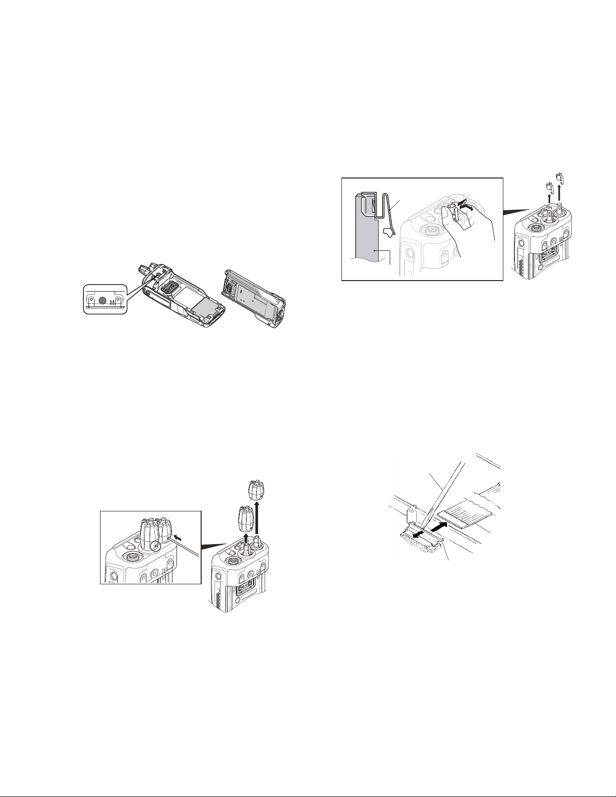
3.2.1 Removing the selector knob and volume knob
(1) Using a thin tool, insert it in the hole on the selector knob
side and push the knob spring. <1>
Note:
When you push the knob spring, take care not to damage the resin of the knob.
(2) Lift and remove the selector knob <2> while pushing the
knob spring.
(3) Repeat steps 1 and 2 for the volume knob, to remove the
volume knob <3>.
(2) Remove the selector knob spring <2>.
Note:
Use minimal contact with your fingers on the knob
spring.
(3) Repeat steps 1 and 2 for the volume knob spring, to re-
move the volume knob spring <3>.
<2>
<3>
Knob spring
Encoder
<1>
Note:
Perform the following procedures when installing the selector knob spring and volume knob spring.
a) Match the direction for the knob spring and the en-
coder.
b) Insert the encoder onto the knob spring until a click
sounds.
3.2.3 How to remove the flat cable
(1) Gently rise up the connector lever in the direction of the ar-
row with a flat-head screwdriver or tweezers. (CN8, CN9,
CN12)
Note:
Gently push both sides of the connector lever, when put
in the flat cable.
Flat-head
screwdriver
Note:
Perform the following procedures when installing the selector knob and volume knob.
a) Match the direction for the hole of the knob and the
knob spring.
b) Push the knob onto the knob spring until a click
sounds.
3.2.2 Removing the selector knob spring and volume knob
spring
(1) Lightly grasp the left and right sides of the selector knob
spring together, and lift up as shown in the figure. <1>
Note:
Do not grasp the knob spring tightly.
Flat cable
Lever
(No.RA018<Rev.002>)1-27
3.2.4 Remove the front case from the chassis
VOID seal
<1>
<1>
<1>
<1>
<3>
<3>
<3>
<2>
<1>
(1) Remove two screws <1>.
(2) Lift the base of the chassis and remove the chassis from
the front case.
Note:
• There is a void seal stuck to the chassis and the front
case, the void sheet peels off of when the chassis is removed from the case. Once the void seal is peeled off,
it cannot be used again.
• When the chassis does not remove from the front
case, remove by pushing in the key top with the finger.
• Regarding VOID, confirm the service policy of the NX5200 to KENWOOD (or authorized distributor).
3.2.5 Remove the holder ASSY from the chassis
(1) Remove the two hooks on the holder ASSY from the chas-
sis. <1>
(2) Rotate the holder ASSY to the right as shown in the figure.
<2>
<2>
(3) Remove the VOL/SEL/MIC FPC from the two holes of the
LCD shielding case. <3>
<3>
<3>
(4) Remove the LCD shielding case from the Main unit. <4>
3.2.7 Removing the Main unit from the chassis
(1) Remove the VOL/SEL/MIC FPC from the connector (CN4).
<1>
(2) Remove the PTT FPC from the connector (CN8). <2>
(3) Remove the Universal connector FPC from the connector
(CN12). <3>
<1>
<1>
Holder Assy
3.2.6 Removing the LCD shielding case from the Main unit
(1) Remove the LCD FPC from the connector (CN9). <1>
(2) Remove the six screws. <2>
<2>
<2>
<2>
<2>
<2>
<2>
1-28 (No.RA018<Rev.002>)
<1>
CN4
<2>
<1>
CN8
CN12
<3>

(4) Remove the six screws <6>.
<6>
<6>
<6>
<6>
<6>
Battery terminal block
<7>
<5>
<1>
<1><1>
<3>
<4>
<2><2>
<1>
Note:
When you remove two screws (black), the battery terminal block is removed.
(5) Anchor the screw hole of the Main unit using the tip of a pair
of tweezers as shown in the figure. Then lift the Main unit
to remove it from the chassis. <7>
3.2.8 Removing the TOP packing
(1) Remove the rear panel by sliding it upwards. <1>
(2) Pull the TOP packing to the left to remove the packing that
is fit into the left groove of the chassis. <2>
(3) Pull the TOP packing to the right to remove the packing that
is fit into the right groove of the chassis. <3>
(4) Pull the TOP packing to the center to remove the packing
that is fit into the center groove of the chassis. <4>
(5) Remove the TOP packing. <5>
Note:
Remove the packing slowly, as the packing of the selector part might be overset when the TOP packing is removed.
If the packing is turned over, return it to the original position using a soft tipped item (e.g., your finger).
3.2.9 Removing the stopper of the selector circle nut and
volume circle nut
(1) Remove the stopper <1> using a pair of tweezers.
<1>
Note:
When reassembling the stopper, install it as shown in the
figure.
Stopper
Chassis
Circle nut
3.2.10 Remove the selector and volume switches from the
chassis
(1) Pull up the cover of the packing. <1>
Volume switch
<1>
Selector switch
Packing
(2) Move the selector and volume switches vertically to lift the
packing.
(3) Pull on the packing and remove it from the chassis.
(No.RA018<Rev.002>)1-29
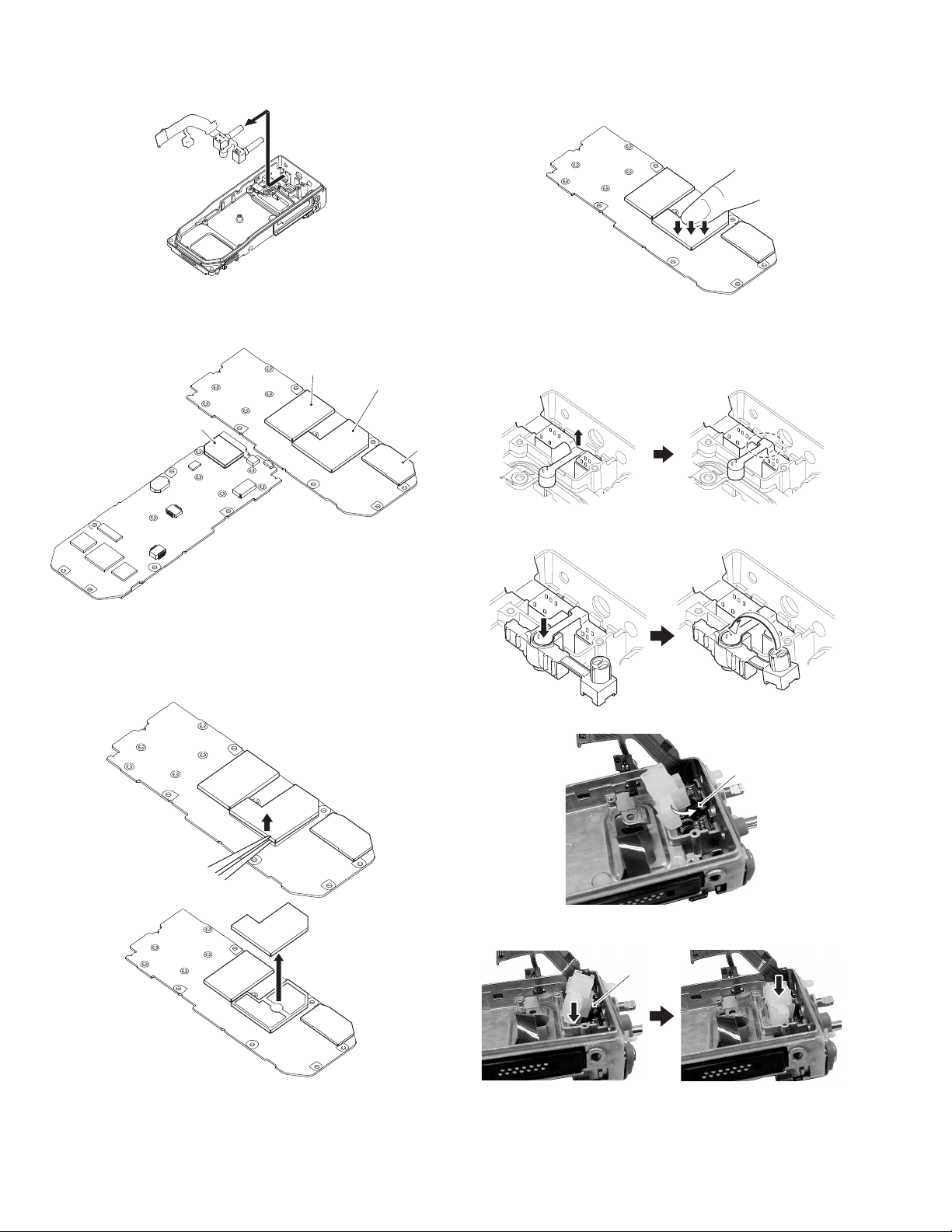
(4) Move the selector and volume switches and then remove
VCO TX
VCO RX
IF
GPS
<1><1>
<2>
<1>
<2>
<3>
<4>
them both from the holes in the chassis.
3.2.11 Remove the top cover from the shield cover
(1) There are four shield covers (GPS, IF, VCO RX, and VCO
TX) on the main unit, the top covers can be removed.
Note:
Push evenly on the top cover and be careful that you do
not bend it as you install it on the shield cover.
3.3 Precautions for Reassembly
3.3.1 Install the packing in the chassis
(1) Lift up the VOL/SEL/MIC FPC as shown by the arrow in the
figure so it is in the shape shown inside the dotted line.
(2) Insert the microphone into the packing. <1>
(3) Insert the cover into the packing. <2>
(2) Use tweezers to slightly lift the edge of the top cover. <1>
(3) As you do step 2 above, vary the position you hold the top
cover as you lift it, and remove the top cover <2>.
Note:
Once the top cover is removed, it cannot be used again.
<1>
<2>
(4) Tuck the packing under the A part of the FPC. <3>
A
<3>
(5) Keep the packing tucked under A as you insert it into the
chassis. <4>
A
<4>
1-30 (No.RA018<Rev.002>)
 Loading...