

Page 1
70%
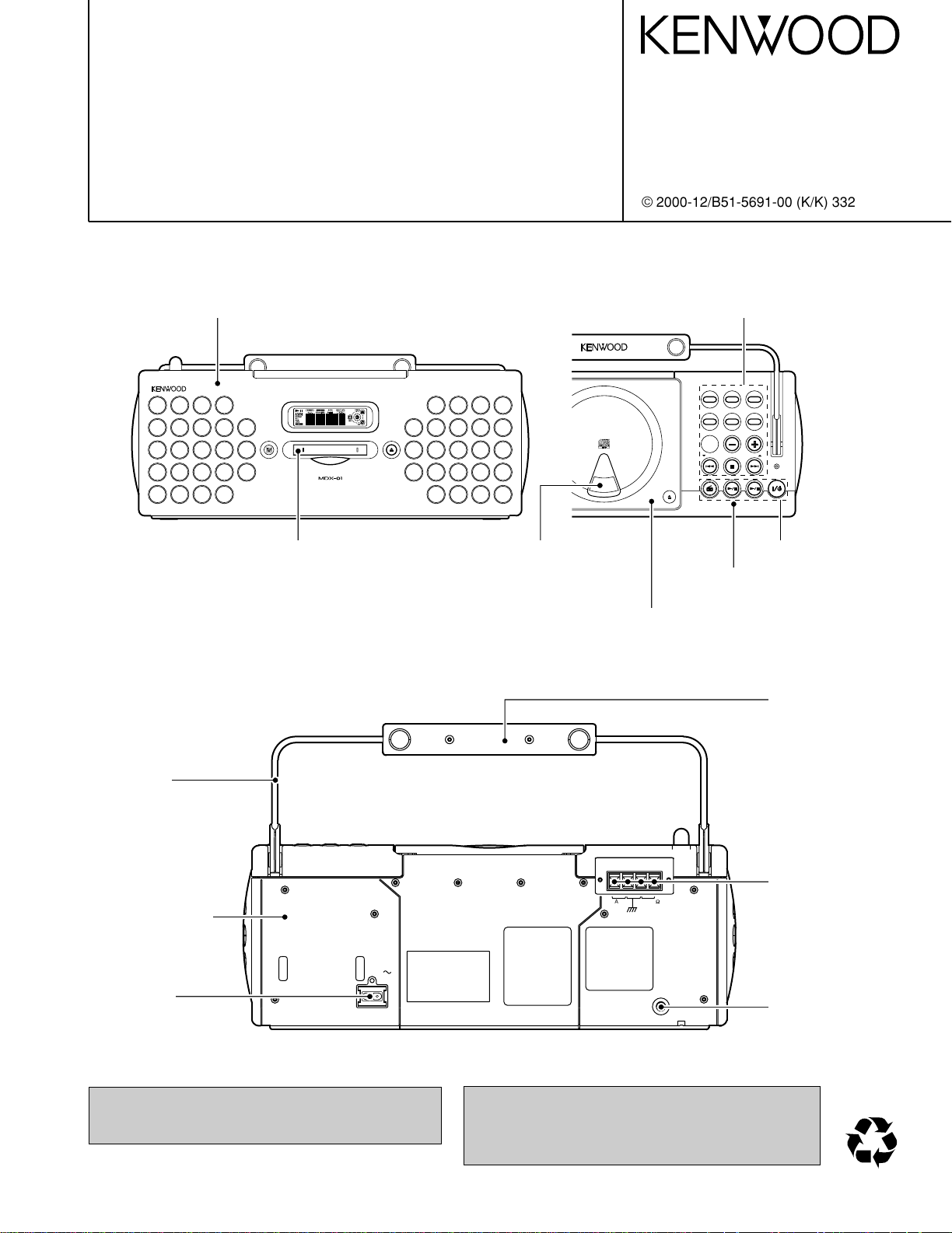
MD PERSONAL STEREO SYSTEM
SOUND
PUSH OPEN
MD RECREPEAT
VOLUME/MULTI CONTROL
TUNER
FM/AM
STANDBY/TIMER
MD
TUNE
MODE
STOP/
CD
MENU
POWER
SET/DEMO
・
C
D
/
M
D
H
i
g
h
S
p
e
e
d
D
u
b
b
i
n
g
S
y
s
t
e
m
・
TUNING
TUNING
MD PERSONAL STEREO SYSTEM
DISC LOADING MECHANISM
EJECT
BEST HITS
FM 75
W
AM
GND
ANTENNA
ANTENNA
PHONES
AC IN
MDX-01/02
SERVICE MANUAL
© 2000-12/B51-5691-00 (K/K) 332
Front cabinet(OUTER) ass'y
(A60-1942-08): L
(A60-1943-08): R
(A60-1944-08): D
(A60-1946-08): H
(A60-1947-08): S
MD door
(A52-0918-08)
Door lens
(B12-0408-08): L
(B12-0409-08): R
(B12-0410-08): D
(B12-0412-08): H
(B12-0413-08): S
Knob A
(K27-7893-08): S
(K29-7895-08): L
(K29-7896-08): H
(K29-7898-08): D
(K29-7899-08): R
Knob B
(K29-7900-08)
Top plate R ass'y
(A60-2059-08): DHLR
(A60-2060-08): S
Door
(A52-0914-08): DHLR
(A52-0915-08): S
Handle(REAR)
(K01-0134-08): L
(K01-0135-08): H
(K01-0137-08): D
(K01-0138-08): R
(K01-0140-08): S
Handle
(K01-0139-08)
Rear cabinet
(A02-2987-08): S
(A02-2988-08): DHLR
AC socket
(E03-0375-08)
D: ORANGE, H: GREY, L: BLUE, R: RED, S: SILVER
In compliance with Federal Regulations, following are
repro-duction of labels on, or inside the porduct relating to
laser product safety.
Note: Please contact KENWOOD service in your side if
you want to get the AC power cord.
Antenna terminal
(E70-0114-08)
KENWOOD-Crop. certifies this equipment conforms to DHHS
Stereo jack
(E11-0398-08)
Regulations No.21 CFR 1040. 10, Chapter 1, Subchapter J.
DANGER : Laser radiation when open and interlock defeated.
AVOID DIRECT EXPOSURE TO BEAM.
Page 2
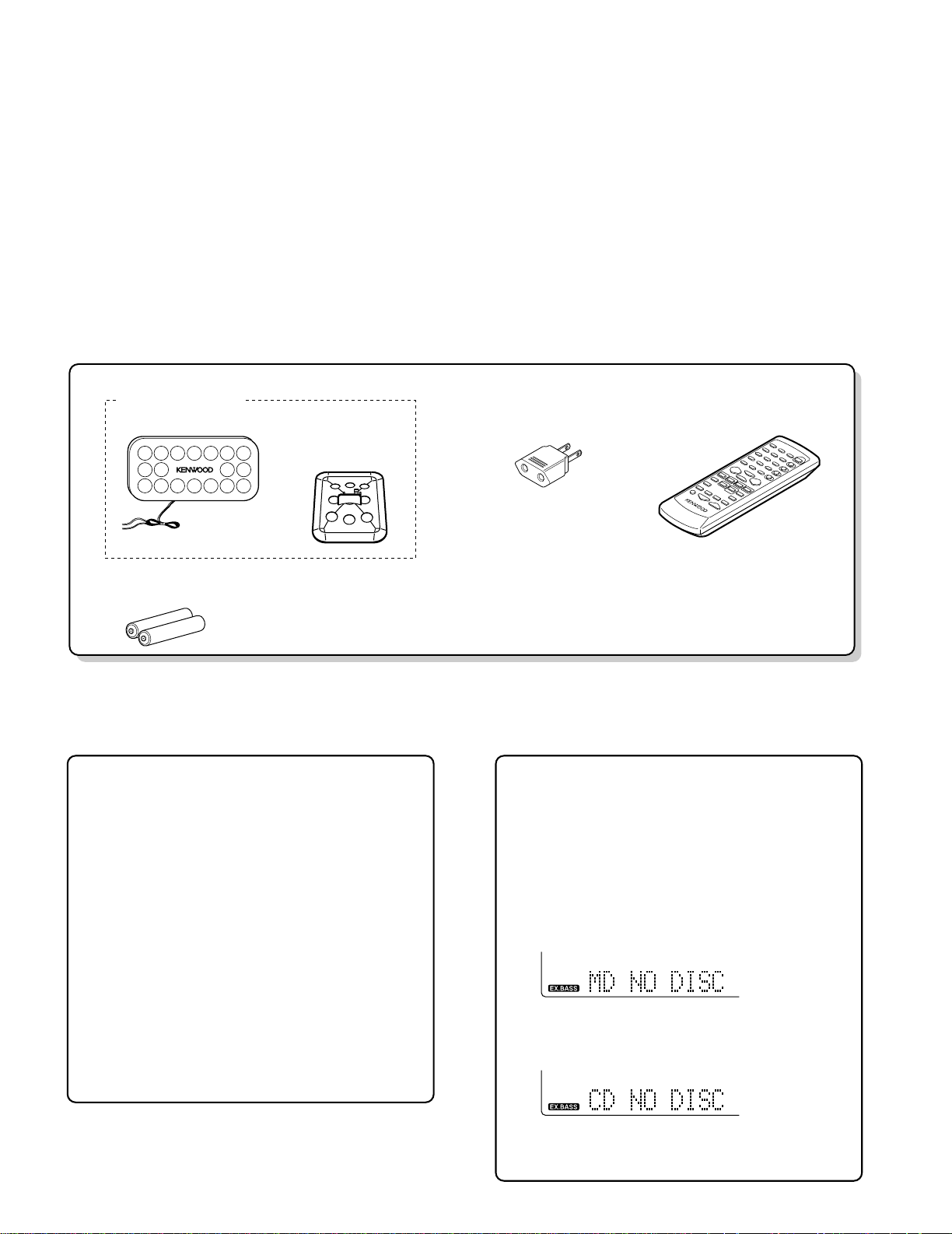
AM loop antenna (x1)
(T90-0868-08)
Remote control unit (x1)
(A70-1440-08): DLH
(A70-1441-08): R
(A70-1442-08): S
Battery cover (A09-1191-08)
R6/SUM-3 batteries
AC plug adaptor
(E03-0115-05)
for remote (x2)
RC
-
MDX0001
AM loop antenna
stand (x1)
(A09-1201-08)
MDX-01/02
Caution on condensation
Condensation (of dew) may occur inside
the unit when there is a great difference in
temperature between this unit and the outside.
This unit may not function properly if condensation occurs. In this case, leave the
unit for a few hours and restart the operation after the condensation has dried up.
Be specially cautious against condensation
in a following circumsatance:
When this unit is carried from a place to
another across a large difference in temperature, when the humidity in the room
where this unit is installed increases, etc.
Note related to transportation
and movement
Before transporting or moving this unit,
carry out the following operations.
(1) Remove the CD or MD from the unit.
(2) Press the 6 key of the MD.
(3) Wait for some time and verify that the
display becomes as shown in the figure.
(4) Press the 6 key of the CD.
(5) Wait for some time and verify that the
display becomes as shown in the figure.
(6) Wait a few seconds and turn the unit
OFF.
CONTENTS / ACCESSORIES
Contents
CONTENTS / ACCESSORIES .................................. 2
DISASSEMBLY FOR REPAIR....................................3
CIRCUIT DESCRIPTION ............................................4
ADJUSTMENT ............................................................8
PARTS DESCRIPTIONS ............................................9
Accessories
PC BOARD .............................................................. 10
SCHEMATIC DIAGRAM .......................................... 13
EXPLODED VIEW ....................................................25
PARTS LIST..............................................................27
SPECIFICATIONS ......................................Back cover
2
Page 3
3
8
4
2
2
1
1
1
1
1
7
1
x3
x2
7
x1
7
x1
10
x1
6
x2
6
x2
5
x2
11
11
11
13
12
12
14
9
x3
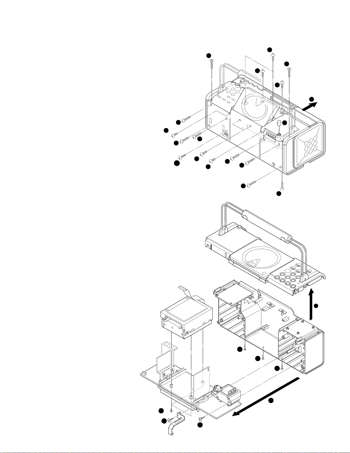
DISASSEMBLY FOR REPAIR
1. How to Remove Front Cabinet
1. Remove 6 screws(1) from the rear cabinet side.
2. Remove 2 screws(2) fixed CD and the front
cabinet.
3. Remove 3 screws(3) from the bottom front side.
4. Move the front cabinet frontwards(4).
2. How to Remove CD and Top Covers
1. Remove 2 screws fixed CD and top covers(5).
2. Remove 8 screws fixed the carrying handle
(6x4) and the rear cabinet(7x4).
3. Turn the antenna cap(8) to remove and lift the
carrying handle and CD mechanism(9).
MDX-01/02
3. How to Remove MD Mechanism
1. Remove the screw(0) fixed the AC inlet socket.
2. Remove 5 screws fixed the bottom cabinet(!x3)
and the power transformer(@x2).
3. Move the main pcb frontwards(#).
4. Remove 3 screws($) fixed the MD mechanism.
3
Page 4
MDX-01/02
CIRCUIT DESCRIPTION
1. INITIALIZATION
1-1 How to Set Initialization
Insert the power cord to AC outlet with pressing REPEAT
key.
1-2 Operation in Initialization mode
Display shows INITIALIZE, and Standby mode after
mechanism check.
The Display shows error code if mechanism has malfunction.
Error Code
CD In 1st figure "C"
MD In 3rd figure "M"
CD Door SW In 7th figure "S"
The until changes to shipment mode after RAM and backup clear, disc out, and so.
2. TUNER PRESET
P.CH BAND FREQ. P.CH BAND FREQ.
1 FM 98.30 MHz 21 AM 531 kHz
2 FM 87.50 MHz 22 FM 87.50 MHz
3 FM 89.10 MHz 23 FM 87.50 MHz
4 FM 108.00 MHz 24 FM 87.50 MHz
5 FM 90.00 MHz 25 FM 87.50 MHz
6 FM 87.50 MHz 26 FM 87.50 MHz
7 FM 87.50 MHz 27 FM 87.50 MHz
8 FM 87.50 MHz 28 FM 87.50 MHz
9 AM 1602 kHz 29 FM 87.50 MHz
10 AM 999 kHz 30 FM 106.00 MHz
11 AM 630 kHz 31 FM 87.50 MHz
12 AM 1440 kHz 32 FM 87.50 MHz
13 FM 106.00 MHz 33 FM 87.50 MHz
14 AM 531 kHz 34 FM 87.50 MHz
15 FM 87.50 MHz 35 FM 87.50 MHz
16 FM 98.00 MHz 36 FM 87.50 MHz
17 FM 98.50 MHz 37 FM 87.50 MHz
18 FM 87.50 MHz 38 FM 87.50 MHz
19 AM 990 kHz 39 FM 87.50 MHz
20 FM 97.70 MHz 40 AM 945 kHz
3. TEST MODE
3-1 TEST Mode Setting
TEST MODE SETTING
CD MD REC
MD 1 SKIP UP Insert the power cord
✽ FTC & Sub-Clock to outlet with pressing
Oscillation Check BEST HITS every left key
Mode
MD mode2 SKIP DOWN
FTC&Sub-Clock Oscillation Check Mode
✽
FTC test mode is after Sub-Clock Oscillation Check
Mode(Internal Oscillation, Check of Period) Check Mode
is 5 times maximum. FTC carries if 1 tlme OK.
The unit is STOP mode after display shows error if 5
times NG.
No Oscillation îERR 1 Period NGîERR 2
(FTC mode is factory use only)
3-2 Test Mode Cancel
The unit cancel the test mode after initialization if pull out
power cord.
The unit cancel the test mode after no initialization if
4
power off.
3-3 Key Function in Test Mode
KEY
CD PLAY
STOP
MENU
SKIP UP
SKIP DOWN
T-SERVO ON(05) uw
T-SERVO OFF(03)
Stop to CD operation(01)
TB/FB (07)
TG/FG (08)
FE/RF (09)
TE/VC (10)
HI SPEED(double speed) uw NOR
SPEED: in playback
Playback in STOP mode.
Track up of CD.
FF search of CD if key pressed
more 400ms.
Pickup move outwards in STOP
mode if key pressed more 400ms.
Playback in STOP mode.
Track down of CD.
FB search of CD if key pressed
more 400ms.
Pickup moves inwards in STOP
mode if key pressed more 400ms.
CD MODE
In STOP mode.
Selfcheck result shows
2 figures
MD MODE 1
–
Stop to operation.
Change to mute-off.
Choose the REC input;
digital or analog in stop
mode.
Track up of MD.
FF search of MD if key
pressed more 400ms.
Track down of MD.
FB search of MD if key
pressed more 400ms.
4. MD TEST MODE FOR ADJUSTMENT
4-1 Entering the Test Mode (MD Mode2)
While pressing the SKIP DOWN key, turn the AC on.
4-2 Cancelling the Test Mode
Turn the AC off.
4-3 Key Operations for Adjustment
KEYS OPERATION
SKIP UP/DOWN Select mode or adjustment value change.
MD PLAY/PAUSE Fix mode or adjustment value.
STOP Cancel the selected mode.
SKIP UP ✽ Pickup moves outwards when pressed skip up key.
SKIP DOWN ✽ Pickup moves inwards when pressed skip down key.
✽ Remote control only.
4-4 Selection of Adjustment Test Mode
Whenever the [volume/multi-control] knob is turned, the
adjustment test mode is selected.
No. LCD DESCRIPTION SECTION
1 TEMP ADJU
2 LDPWR ADJU Laser power adjustment. 5-6
3 LDPWR CHEC Laser power check. 5-6
4 EFBAL ADJU Traverse adjustment. 5-7
5 TE B. ADJ Automatic EF balance adjustment. 6 FBIAS ADJU Focus bias adjustment. 5-8
7 CPLAY MODE Continuous playback mode. 4-5
8 CREC MODE Continuous recording mode. 4-6
✽9 STT-LIMIT
✽10 JUMP MODE Track jump checking mode. -
✽11 SRV DAT RE Servo data reading. -
✽12 EEP MODE E2PPROM data reading or rewrite. -
✽13 EEP INITIAL E2PPROM data initializing. -
For more information on each adjustment mode, refer to
each section of 5, "Electrical adjustment".
If other adjustment mode has been entered incorrectly,
press the STOP key to exit the mode.
✽ The number 9 - 13 are not used for service. If these
mode have been entered incorrectly, press the STOP
key immediately to exit the mode. Specially, do not use
EEP INITIAL. (E2PROM data has initialized if used it.)
The work of adjustment is unnecessary
in this mode.
Check the mechanism start limit
switch position.
5-5
-
Page 5
MDX-01/02
1. Setting of Continuous Playback Mode
No. Key
1
4 ¢
Select [CPLAY MODE]
2 Load disc
3 PLAY [CPLAY MID]
[c=xxxx a=yy] error
(xxxx=C1 error, yy=ADIP error)
[CPLAY OUT]
[c=xxxx a=yy] error
(xxxx=C1 error, yy=ADIP error)
4 STOP
[CPLAY MODE]
2. Change of Playback Points(in continuous playback mode)
No. Key
Display/Function
Display/Function
1
PLAY
2
[CPLAY IN]
[c=xxxx a=yy] error
(xxxx=C1 error, yy=ADIP error)
PLAY
3
Carry out No.1 to 3 in the above table.
4
5
STOP [CPLAY MODE]
EJECT Disc out
1. Continuous Recording Setting
No. Key Display/Function
1
4 ¢
Select [CREC MODE]
2 Load the recordable disc
3 PLAY [CREC MID]
4 PLAY [CREC (zzzz)] CREC address
(0300h cluster=recording start point)
5
STOP [CREC MODE]
2. Change and End of Recording Points
1 Carry out No.1 to 3 in the above table Select[CREC MID]
2
¢
[CREC OUT]
3 PLAY [CREC (zzzz)] CREC address
(0700h cluster=recording start point)
4 STOP [CREC MODE]
6
5
¢ (2time)
Select [CREC IN]
7 PLAY [CREC (zzzz)] CREC address
(0300h cluster=recording start point)
8 STOP [CREC MODE]
PLAY [CREC MID]
9 EJECT Disc out
Pick-up
Flexible board
Laser tap
No.
Key Display/Function
1
4 ¢
Select [TEMP ADJU]
2 PLAY [TEMP=xx (yy)]
(xx=compensation data, yy=setting temperature)
3
4 ¢
Input "yy" with present temp..
4 PLAY [TEMP=✽✽SAVE] in writing data
[TEMP ADJU ST]
CIRCUIT DESCRIPTION
4-5 Continuous Playback Mode
4-6 Continuous Recording Mode
1. The recording start addresses of IN, MID, and OUT are
described below.
IN 30H cluster
MID 300H cluster
OUT 700H cluster
2. An erasure prevention control is not detected in the test
mode. Be careful not to enter the continuous recording
mode using a disc containing the data that should not be
erased.
3. Do not record continuously for more than five minutes.
4. Take care that no vibration is applied during continuous
recording.
5. ELECTRICAL ADJUSTMENT
5-1 Precaution during confirmation of Laser
Diode emission
During adjustment, do not view the emission of a laser
diode from just above for confirmation. This may damage your eyes.
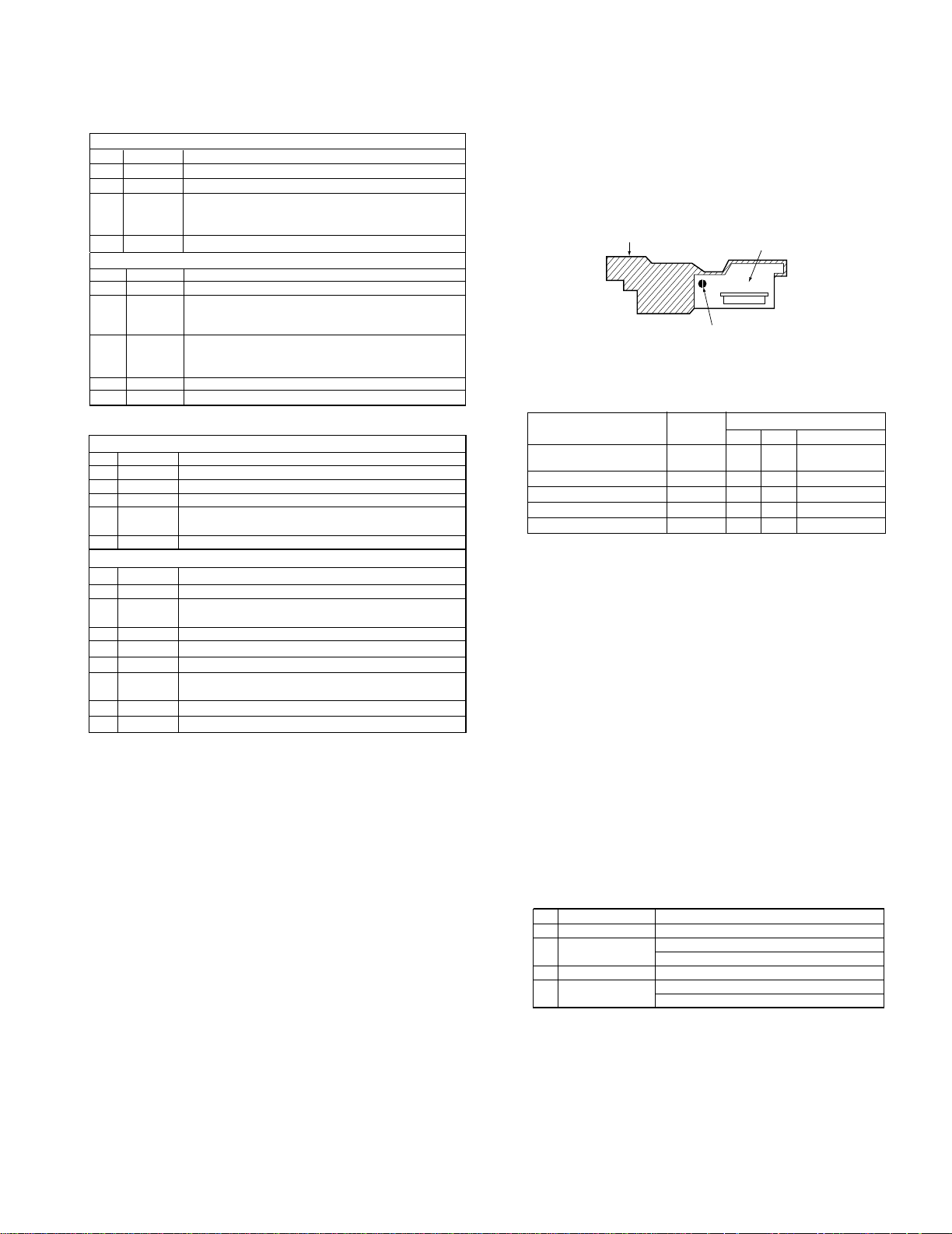
5-2 Precaution on handling of Optical pick-up
(KMS-260B)
The laser diode in an optical pick-up is easy to be subject to electrostatic destruction. Therefore, solderbridge the laser tap on the flexible board when handling the optical pick-up.
When removing the flexible board from the connector,
make a solder bridge in advance, then remove the
board. Be careful not to remove the solder bridge before
inserting the connector. Moreover, take careful measures against electrostatic destruction. The flexible
board is cut easily. Handle the flexible board with care.
5-3 Precaution during adjustment
1) Perform the adjustment and confirmation marked with “O”
in the order shown in the table when the parts below are
replaced.
Optical BD board
1.Temperature compensation offset adjustment X O O O
2.Laser power adjustment O O X O
3.Traverse adjustment O O X O
4.Focus bias adjustment O O X O
5.Error rate confirmation O O X O
pick-up IC6 D101 IC1,IC2,IC10
2) In the test mode, perform the adjustment. After adjustment is completed, cancel the test mode.
3) Perform the adjustment in the order described.
4) Use the following tools and measurement equipment.
• CD test disc TGYS-1
• Laser power meter
• Oscilloscope (with bandwidth of more than 40 MΩ)
(Calibrate the probe before measurement.)
• Digital voltmeter
• Thermometer
5) Take care that VC and GND (ground) are not connected
on the oscilloscope when two or more signals are monitored on the oscilloscope. (VC and GND are short-circuited in this case.)
5-4 Creating the recordable continuous recording
disc
This disc is used for focus bias adjustment and error rate
confirmation. How to create the recordable continuous
recording disc is 4-6.
5-5 Offset Adjustment
5-6 Laser Power Check and Adjustment
Laser power setting in playback and recording modes.
Preparation
1. Remove the MD mechanism from the unit.
2. Connect the digital voltmeter to IOP1 and 2 on X33 pcb.
3. Remove the top plate from traverse unit.
4. Remove the magnetic head.
5. Remount the MD mechanism to the unit
5
Page 6
MDX-01/02
1. Recordable Disc
No. Key Display/Function
1 Connect the oscilloscope to TE1 and VC in X33 pcb
2 4 ¢ Select [EFBAL ADJU]
3 Load the recordable disc
4 PLAY [EFBAL MO-W]
5 PLAY [EF=$✻✻MOW]
6 4 ¢
Write power adjustment. Adjust the waveform as follows.
7 PLAY Display shows [EF=$✻✻MOR] after [EFB=✻✻xSAVE]
to save the data in E2PROM.
Mode changes write to read
Focus and disc servo are on. Tracking servo off.
8 4 ¢
Read power adjustment. Adjust the waveform as follows.
9 PLAY
Save the data in E2PROM.
Display shows [EFBAL MO-P]
PLAY Display shows [EF=$✻✻MOP]
(Pickup travels to search pits and tune the servo to on.)
10 4 ¢ Adjust the waveform as follows.
11 PLAY Display shows[EFB=✻✻xSAVE]
to save the data in E2PROM.
Display shows [EFBAL CHAN]
12 EJECT Unload disc.
2. Pre Master Test Disc(TGYS-1)
No. Key Display/Function
1 Load the disc(TGYS-1). [EFBAL CD]
2 PLAY
PLAY
[EF=$✻✻CD] servo is on
3 4 ¢ Adjust the waveform as follows.
4 Save the data in E2PROM.
Display shows[EFB=✻✻xSAVE] in brief time.
[EF PHASE]
5 EJECT Unload disc.
(TE1)
330kΩ
10pF
(VC)
Oscilloscope
+
-
TE1
VC
Oscilloscope
X33
ADJUSTMENT
+
-
V: 0.5V/div H: 10ms/div
INPUT: DC mode
+
-
Laser
power meter
Digital
voltmeter
Objective lens of
optical pick up
IOP2
IOP1
X33
ADJUSTMENT
1. Laser Power Adjustment
No. Key Display/Function
1 4 ¢ [LDPWR ADJU]
Load recordable disc
2
Load the disc and lazer on
[(a0.9mW) $xx] read power
(xx=power value)
43EJECT
PLAY
Unload the disc and laser on
5 PLAY [LDPWR CHECK]
6 1 ¡ Move the pickup to check the laser power with
laser power meter sensor
7 4 ¢
Adjust "xx" so that the power meter shows 0.9mW.
8 PLAY [(a7.0mW) $xx] writing power
9 4 ¢ Adjust "xx" so that the power meter shows 7.0mW.
This adjustment should be carried out in 15 secs.
10 PLAY Laser power off
Display shows [LDPWR ADJUST] after [LDPWR<$xx]
to save the data in E2PROM
Start from No.2 if readjust.
2. Laser Power Check
No. Key Display/Function
1 4 ¢
[LDPWR CHEC]
2 PLAY [(c0.9mW) $xx]
(xx=0.85 to 0.95mW)
3 PLAY [(c7.0mW) $xx]
Laser power meter: 7.0±1.0mW✽
VOM:optical pickup indication value ±10%✽
✽ In this case, lop = 82.5 mA
lop(mA) = Reading of digital voltmeter(mV)/1(Ω)
(optical pick-up label)
KMS
260B
27x40
B0825
CIRCUIT DESCRIPTION
6
5-7 EF Balance(Traverse Adjustment)
Connection :
During this adjustment, the oscilloscope changes in units
of about 2%. Adjust so that the waveform comes nearest
to the specified value. (MO groove read power traverse
adjustment)
(Traverse waveform)
Specification : A = B
Notes :
1. Data is erased during MO write when a recorded disc is
used for this adjustment.
2. If the traverse waveform is difficult to be monitored, connect an oscilloscope as shown in the figure below.
Page 7
A/D keys
EEPROM Write
M30624MG-308FP
RELAY
POWER key
RESET
LED
Remote
key
LCD Back
Light
LCD CD
MD
DSP
u-COM
Control
KEY1-3
V.DET.
SENS
CLOSE
TUNER ON/OFF, SA CLK,
SA DATA
ST, SD,PLL DO
MD CE
SQSO
LCDSDA
LCDCS
LED0, LED1
BL0,BL1
REMOCON
RESET
RELAY
SCL
SDA
SCOR
CRXD CTXD
LCDRS
LCDSCL
LCDRES
SQCK MD RST
CLS SW
CD POWER, LDC,HI SP. SCLK. CD CLK.XLAT.CD DATA.XRST
AC/BATTERY
CD Door
Control
TUNER PLL
IC
SYSTEM IC
LC75396NC
TUNER
SYSTEM IC
MDX-01/02
No. Key Display/Function
1. CD Error Rate
1
4 ¢
[CPLAY MODE]
2 Load the test disc(TGYS-1)
3 PLAY Display shows [CPLAY MID]
Access end
[c=xxxx a=yy] xxxx=C1 error (lower 20) yy=AIDP error
4 STOP [CPLAY MODE]
5 EJECT Unload disc.
2. MO Error Rate
No. Key Display/Function
1
4 ¢
[CPLAY MODE]
2 Load the recordable disc
3 PLAY Display shows [CPLAY MID]
Access end
[c=xxxx a=yy] xxxx=C1 error (lower 50) yy=AIDP error(00)
4 STOP [CPLAY MODE]
5 EJECT Unload disc.
No. Key Display/Function
1
4 ¢
Select [FBIAS ADJU]
2 Load the disc.
3 PLAY [a=xx yyyy/] point a
(xx=focus bias, yyyy=C1 error)
4
4 ¢
Adjust "yyyy" to 220
✻
5 PLAY [b=xx yyyy/] point b
6
4 ¢
Adjust "yyyy" to 220
✻
7 PLAY [C=xx yyyy/] point c
Check "yyyy" within 50
8 PLAY Display shows [aa bb cc(xx)] focus bias adjust
(aa= point a,bb=b,cc=c )
CIRCUIT DESCRIPTION
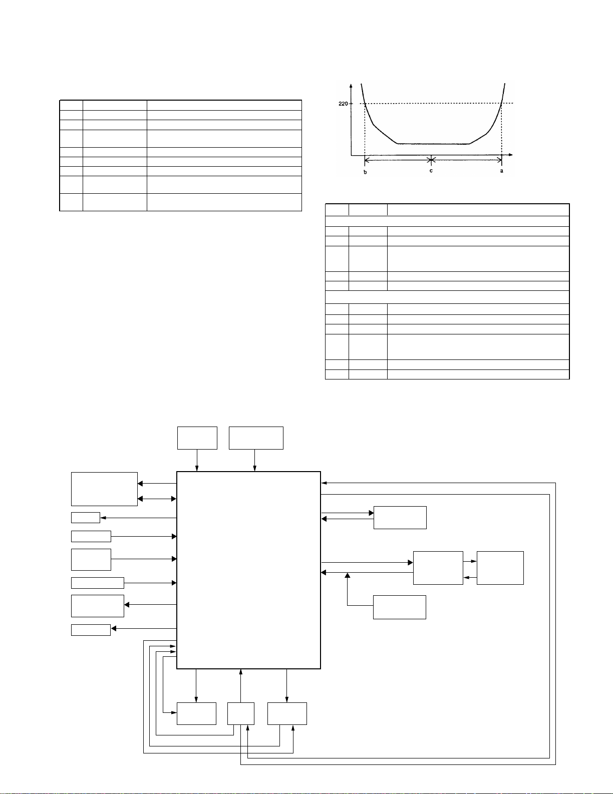
5-8 Focus Bias Adjustment
Use the special disc(continuous recorded disc)
* Notes :
1. The relation between the C1 error and focus bias value
is shown in the figure below. Points "a" and "b" in the
figure are detected by the above adjustment. Focal
position "C" is automatically obtained from points "a"
and "b" by calculation.
2. The C1 error rate fluctuates. Therefore, perform the
adjustment according to the observed mean value.
C1 error
Focus bias value
5-9 Error Rate Check
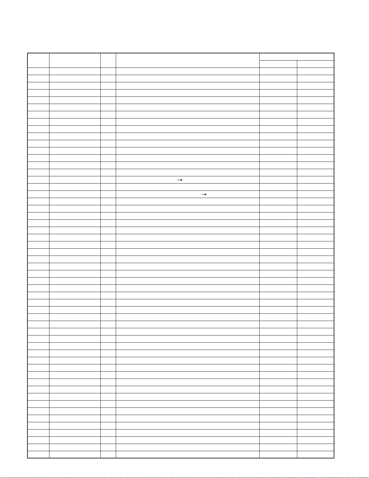
6. Microprocessor: M30624M-308FP(IC401)
6-1 Periphery Block Diagram
7
Page 8
MDX-01/02
6-2 Microprocessor's Port Description
Port # Port Name I/O Description
1~3 NC - No use
4 SDA O EEP ROM data
5 SCL O EEP ROM clock
6 RELAY O Main power supply control ON OFF
7 CE I No power supply detection AC ON AC OFF
8 BYTE - GND
9 CNVSS - GND
10 XCIN I Oscillation for clock(32.768MHz)
11 XCOUT O Oscillation for clock(32.768MHz)
12 RESET I Microprocessor reset port NORMAL RESET
13 XOUT O Oscillation for main clock(10MHz)
14 VSS - GND
15 XIN I Oscillation for main clock(10MHz)
16 VCC(B.U.) I Standard voltage for A/D converter(+5V)
17 NMI I +5V
18 REMOCON I Remote control signal H L: interrupt
19 POWER KEY I Power key signal control other backup
20 SCOR I Sub-code synchro signal control L H: interrupt
21 LCD RS O Reset port of LCD driver
22,23 NC - No use
24 B.L.0 O Back light dimmer. L=dark, H=bright(#26 port(B.L.1)=L)
25 LED0 O Standby led control OFF ON
26 B.L.1 O Back light dimmer. H=dark, L=bright(#24 port(B.L.0)=L)
27 LED1 O Timer led control OFF ON
28 LCD CS O CS port of LCD driver
29 CTXD O TXD port of UART
30 CRXD I RXD port of UART
31 LCD DATA O Data port of LCD driver
32 NC - No use
33 LCD CLK O Clock port of LCD driver
34 LCD RST O Reset port of LCD driver
35 NC - No use
36 SQSO I CD sub-code
37 SQCK I Clock for CD sub-code
38 MD CE O MD IC CE
39 MD RST O MD reset signal RESET NORMAL
40~55 NC O No use
56 CD ON/OFF O CD power control ON OFF
57 NC - No use
58 AMUTE O Audio mute signal OFF ON
59 TU CLK O PLL/SYSTEM IC clock
60 ST I Tuner stereo signal MONO STEREO
61 SD I Tuning signal NO TUNED
62 VCC(B.U.) O No use
63 NC - No use
64 VSS - GND
65 TU DATA O PLL/SYSTEM IC data
66 TU CE O PLL/SYSTEM IC CE
67 PLL DO I PLL IC data
68 NC - No use
69 LDC O CD laser control ON OFF
70 CLS SW I CD door close detection OFF ON
71 OPN SW - No use
72 CLOSE O No use
8
CIRCUIT DESCRIPTION
ACTIVE
HL
Page 9
MDX-01/02
CIRCUIT DESCRIPTION
Port # Port Name I/O Description
73 OPEN O No use
74 HI SP O Recording signal in high speed mode NORMAL
75 SCLK O CD sense clock
76 SENS I CD sense
77 CD CLK O Clock for CD DSP
78 XLAT O Latch for CD DSP
79 CD DATA O Data for CD DSP
80 CD XRST O Reset for CD DSP NORMAL RESET
81 CODE I Model selector
82 CODE I Model selector KITTY NORMAL
83 CODE I Model selector
84~87 NC - No use
88 LOOP - No use
89,90 NC - No use
91 V.DET I AC power supply detection(less 1.25V:detect)
92 NC O No use
93~95 KEY1~3 I Key signal ON OFF
96 AVSS - GND
97 NC - No use
98 VREF I Standard voltage for A/D converter
99 VCC(B.U.) I Standard voltage for A/D converter(+5V)
100 NC O No use
ACTIVE
HL
6-3 Key Matrix
✽ Reference voltage=5V.( )=Port of Microprocessor
Voltage[V] 0.00~0.46 0.47~1.32 1.33~2.14 2.15~3.00 3.01~3.80 3.81~4.60 more 4.61
KEY 1
(#93) EJECT
KEY 2
(#94)
KEY 3
(#95) DOWN
- SKIP UP
POWER CD BEST HITS TUNER REPEAT SOUND KEY OFF
STOP
SKIP
MD
VOL.+ VOL.- MD MD RE KEY OFF
SET/DEMO MENU - KEY OFF
9
Page 10

MDX-01/02
CD section
NO. ITEM
INPUT
SETTINGS
OUTPUT
SETTINGS
CD PLAYER
SETTINGS
ALIGNMENT ALIGN FOR FIG.
TEST MODE : While pressing the MD REC key ,plug the power cord into the AC power wall output.
Load the TEST DISC.
[1]
LASER CURRENT
CHECK
Test disc
type 4
Connect the DC voltmeter
across R208A (Q201-E)
Press the PLAY/PAUSE
key to check that the
display is 03 or05.
-
220~550mV
CH1:RF
GND:REF
[2]
Note:
• Type 4disc: SONY YEDS -18 Test Disc or equivalent.
• Keep the step of adjustment.
FOCUS ERROR
BIAS
(Set up horizontally)
Test disc
type 4
Connect an oscilloscope
as follows.
Press the PLAY/PAUSE
key . Confirm that the
display is 05.
VR 201
Optimum eye pattern
Tuner section
NO. ITEM
INPUT
SETTINGS
OUTPUT
SETTINGS
RECEIVER
SETTINGS
ALIGNMENT
POINTS
ALIGN FOR FIG.
FM SECTION: SELECTOR: FM
1
TUNING LEVEL
98.0MHz MONO
1 kHz, ±40kHz dev.
30dBf (ANT. input)
–
MONO 98.0 MHz
TUNER PACK
VR 101
Adjust VR101 and
stop at the point where
LCD801(TUNED)
goes on.
ADJUSTMENT
10
Page 11

MDX-01/02
PARTS DESCRIPTIONS
11
Page 12

A BDCE
R504A
R505A
R514A
R513A
R517A
R518A
R519A
R516A
R515A
R520A
R512A
R510A
R508A
R507A
R509A
R503A
R502A
R501A
R511A
R506A
CN802
R813A
110
R814B
R811A
R810A
R815A
C808A
R801A
C807A
R802A
C802A
R803A
C804A
R804A
C803A
R809A
R808A
R807A
R806A
J503
J508
J504
J502
CDTUNER MD
POWER
SKIP DOWN
CD DOOR
STOP
VOL. DOWN
VOL. UP
SOUNDSET / DEMOMENU
REPEAT MD REC. BEST HITS
SKIP UP
J501
J505
J506
J507
E
8
1
E
BB
SW513
Q501
Q502
SW512
SW514
CN501
SW516
SW508
SW507 SW511
SW501
SW502SW509SW504
D502
SW515
SW506
SW505
KEY UNIT
SW510 SW503
SW801
D802
D801
IC801
VR801
MD EJECT
J802
10
13
1
J802
C809
CN801
DISPLAY UNIT
PC BOARD (Component side view
1
2
3
)
4
5
6
7
12
Refer to the schematic diagram for the value of resistors and capacitors.
Page 13

FHJ LNGIKMO
R708A
C706A
R716A
R709A
R703A
R705A
R706A
R704A
R707A
C406A
R410A
R407A
R473A
R464A
R462A
C422A
R313A R314A
R465A
C413A
R460A
R461A
C423A
R435A
R436A
R481A
C425A
C412A
R469A
R453A
R417A
R418A
R419A
R423A
R420A
R421A
R422A
R424A
R425A
R429A
R430A
R428A
R427A
R451A
R484A
R456A
R454A
R457A
R715A
R713A
R468A
R434A
R425A
R455A
R445A
R450A
R305A
C353A
R478A
R490A
R477A
R316A
R315A
R617A
R621A
R622A
R623A
R487A
R489A
R488A
C629A
C618A
R603A
C607A
R607A
R628A
C631A
C603A
C604A
C632A
R611A
C608A
R608A
C627A
C628A
R620A
R626A
R624A
R627A
R625A
R308A
R307A
R306A
C625A
C630A
C313A
C319A
C321A
C323A
C315A
C317A
R318A
R317A
C355A
C356A
C354A
C339A
R411A
C348A
C344A
C345A
R448A
R447A
R416A
R415A
R437A
R438A
R439A
R440A
R441A
R442A
R443A
C401A
R444A
R491A
C311A
R301A
R302A
R304A
R303A
R605A
R606A
R604A
C301A
C338A
C616A
R612A
C310A
C349A
C350A
C302A
C312A
C314A
1
64
49
48
33
32
17
16
C316A
C619A C620A
C318A
C320A
C322A
C324A
C330A
C329A
C335A
R601A
R602A
C309A
IC301
C621A
R632A
C417A
C411A
R414A
C416A
IC401
R407B
R408A
R408B
R402A
R402B
R449A
R446A
R485A
R480A
30
100
81
80
1
51
50
31
R405A
R470A
R476A
R458A
R463A
R412B
R412A
C408A
C407A
C409A
R467A
R431A
R406A
R433A
R432A
C405A
R479A
C424A
R413A
R459A
R466A
C410A
R471A
R474A
C402A
R404A
C403A
R403A
C404A
R475A
R472A
R486A
R426A
R492A
R409A
C704A
C705A
R702A
R701A
D710A
C1A
R104A
R159A
C108A
R134A
R136A
R122A
R154A
C117A
R119A
R117A
R5A
R1A
C2A
C124A
C126A
C131A
C130A
C128A
C114A
C140A
C148A
R13A
C11A
R7A
R8A
C17A
R14A
C12A
C8A
C156A
C122A
C138A
C141A
C146A
C144A
C143A
R152A
C137A
R148A
R129A
R10A
C13A
R123A
R126A
R144A
R124A
R125A
R145A
R115A
R113A
R114A
R127A
R153A
C101A
C111A
R105A
R101A
C147A
C9A
R2A
C6A
C5A
C3A
R6A
C16A
R4A
R19A
C10A
C105A
C139A
R11A
C145A
R130A
C115A
C7A
R3A
C4A
C164A
R155A
R142A
R133A
R121A
R118A
R151A
R149A
R108A
R120A
R134A
R111A
R132A
R131A
R137A
R136A
R135A
R158A
R138A
R147A
R146A
C161A
C162A
C158A
C159A
R106A
R103A
C113A
C112A
C157A
C109A
C110A
R150A
R102A
C103A
C102A
C104A
IC201
IC202
R213A
R214A
R265A
R262A
C241A
R267A
R261A
R247A
R248A
R243A
R249A
R240A
C225A
R241A
R242A
C224A
R234A
C238A
C244A
R236A
C222A
C246A
C245A
R232A
R252A
R254A
C232A
R256A
R266A
C230A
R233A
21
20
60
61
180
40 41
C208A
R220A
C209A
C207A
R251
R263
R218
R219
R250
R258A
R208B
R217A
R216A
C248
R211
R212
R215
C205
C204
R208A
C240A
R204A
R259A
R260A
R203
R205
R246A
C227A
C247A
R223AR221A
C211A
C212A
C210A
R226A
R224A
C242A
R225A
R227
C213
C215
C214A
R228
R229A
C216A
C243A
C217A
C239A
C218AC219A
C231A
R257A
C229A
R255A
C233A
C237A
C234A
R253A
R231A
R264A
R239A
C223A
R235A
R238A
R237A
R201
R262
R202A
R206A
1
10 11
20
C167
C105
C34
C35
R105
R15
R16
R117
R106
L6
L9
R212
C302
R208
C300
R108
R214
C303
R210
C306
R200
R215
R203
C305
R211
R202
R109
R201
C301
C117
C133
R213
R209
C307
R205
R204
R207
R206
R8
R9
R145
C189
C320
W209
R161
R115
R52
R125
R127
R144
C322
R53
R3
R4
X2
R186
R187
R218
C158
C188
R166
C107
C115
L7
C116
L8
R228
C171
R217
R175
R184
R188
R190
R189
R177
R180
R158
R159
R147
R169
R137
R220
R219
R1
W108
C304
C163
C325
R229
R216
R224
W200
R174
R173
R149
R123
R223
R227
C324
C326
C328
8
28
DIN2
3.3V
DIN1
126
MGND
AOUTL
CRXDCEBON
SRD
SWD
M3
SEN
CTXD
1
50
75
25
1
1
10
11
20
BACKV
FRDT
ADR
MUTE
HGND
H5V
L-
L+
1
HMU
MOD
D
B
A
J
VC
XINT
RECP
RF
FE1
FE2
IOP2
MOD
GND
C
F
E
TR+
TE2
50
75
25
1
FFD
FRD
SRD
SFD
MNT0
EFMO
F-
LM+
3.3V
TR-
IOP1
XLA
SQS
DQS
TE1
100
AOUTR
GND
SLT
ID
HP
MDEL
MNT1
MNT3
SWDT
SCLK
SPR
SPF
MNT2
TRD
GND
VDD
1
15
14
ADDT
DOUT
CTX
1
13 24
25
37
SRDT
SENS
RECP
XLAT
AINR
8
116
AINL
RMS
XRST
100
M2
M0
M1
SDA
5
8
SCL
4
1
9
MUT
256
EMP
BCK
GND
XINT
D3.3V
TX
10
20
11
4M
EFM
HEAD2
HEAD1
RECP
CRX
H POS
VC
TX
LRCK
ADDT
DATA
PD
A+5
AGND
DG
GND
TFD
ILCC
F+
SCL
LDON
LM-
I
D+5
M+5V
EMPH
FWDT
L5
E
1
2
3
5
B
EB
RST
EB EB
EB
26
76
51
36
48
12
26
51
76
CN1
Q2
CN5
IC2
Q6
IC6
IC5
Q1
Q4
IC1
Q21
IC7
Q22
IC24
IC8
IC12
D704
POWER UNIT
D703
Q703
D406
Q702
D709
D403
CN603
CN401
IC402
D402
Q403
Q406
CN407
CN402
Q402
Q401
Q407
CN404
Q405
D404
D405
CN406
CN403
Q609
Q610
IC302
Q604
CN605
Q608
Q607
D604
IC601
JK602
PHONES
AC IN
IC403
D409
D401
D408
D407
D603
D601
D712
Q704
D702
D701
Q701
C702
B
E
B
E
B
BE
B
B
O
G
I
E
E
E
BE
T702
RL701
F701
F702
BD701
C703
J703
C708
C709
1
1
4
8
5
8
1
1
25
2
26
E
B
E
E
3
B
B
1
E
E
E
B
B
B
E
B
EBE
B
EB
18
10
1
10
1
113
R714
J702
R712
R711
R710
J705
J706
J707
J708
J436
J434
J430
J429
J428
J427
J403
J431
R713
C701
JK701
J440
C419
C420
C414
C341
C340
C306
C305
C351
C622
C623
C342
C344
C357
C358
J602
C611
C612
C614
C601
C624
C626
C303
J312
J301
C304
C337
1
4
C326
C328
C334
C332
C336
C331
C325
C327
C333
C605
C606
C602
C610
C609
J601
C613
J603
R613
R610
Q601
Q602
R609
R614
C617
C615
J406
J422
J454
L401
L403
L404
L402
C421
J441
J444
J443
J468
J447
J448
J445
J455
J421
J420
J419
J418
J426
J425
J424
J423
J402
J417
J416
J415
J461
J459
J413
J412
J411
J410
J409
J408
J401
J462
J463
J466
J407
J404
J606
R310
J451
J458
J604
J310
J311
J309
J307
J306
J305
J304
J303
J302
R312
J315
J308
R629
R630
J464
J460
J467
J450
J446
J453
C359
J456
J457
J605
J438
J439
J435
J437
J414
J449
J469
J433
J432
J701
T701
C707
J442
X401
X402
D707
D708
L2
T1
T2
J101
L101
CF102
C153
C106
L4
L102
J118
J119
J117
C116
C121
C120
R107
C119
C118
C151
C123
C142
J120
X101
R110
C132
C129
C127
C125
C152
C133
C145
C134
C135
J107
J108
J104
J105
C154
J115
T102
VC101
1
E
E
B
B
EB
EB
E
1
1
10
32
17
1
16
11
12
22
B
4
TP101
CF101
TC1
L1
T101
T103T104 CF103VR102
J114
J113
J112
J111
J110
J109
J116
C107
J102
J103
J3
J2
J1
J106
VR101
VC2
TC101
VC1
D104
TUNER UNIT
Q2
Q3
Q101
D103
Q102
D101
D102
Q1
CN101
D105
IC102
JK101
IC101
J204
J201
J202
TP201
1
1
118
16
32
17
2
C202
C203
VREF
RF
J221
J226
C238
C220
J228
J229
J230
J231
C226
J213
J212
J211
BE
C228
J233
J210
J223
J225
J224
J227
J222
C237
J219
L201
J206
+5.0V
LD
C201
EB
BE
EB
J220
D201
J214
J208
J207
R244
J232
VR201
J215
J216
J217
J218
J209
X201
J205
15
1
6
1
16
2
J203
J234
CN201
CD UNIT
Q204
CN203
CN204
CN202
IC203
Q201
Q202
Q203
D202
C311
R139
R17
C13
W208
R14
W7
X1
C131
W207
R113
C151
R164
L5
R141
R181
R163
C106
R162
C108
R176
R104
L50
C198
R13
C111
R148
R150
R146
W5
C124
C129
C109
C134
C122
R6
R5
R167
R165
R7
C110
C144
C143
C142
C128
C132
C135
C130
C118
C46
R103
R112
R170
R121
R110
R142
R143
R133
R134
R131
R132
R140
R135
R136
C187
C190
R171
R225
R178
R172
R182
R183
R41
R40
L51
C200
C12
L11
W6
C121
C136
C321
C152
C112
C123
C102
C181
R185
R179
R107
C312
C39
C38
C103
C104
C101
C119
W210
C166
C169
C316
C168
C31
C44
C185
C186
C327
C164
R160
R168
C170
R10
R11
C184
X3
R114
R111
R226
W206
R18
C32
C113
W205
C310
C313
C314
C315
C317
C318
C319
W220
W221
21
1
1
10
1
4
SL+
SL-
1
SP-
SP+
E
B
XRST
56
EB
B
E
EB
B
E
EB
EBEB
EB
EB
2
20
2
10
11
3
2
OGI
Q5
Q7
Q3
CN4
CN3
Q8
D11
Q11
Q10
D101
D1
D2
Q23
IC30
Q20
IC10
D12
D13
D10
CN2
Q13
Q12
X33-1270-00 (J70-1453-22)
PC BOARD(Component side view
1
2
3
4
5
6
7
Refer to the schematic diagram for the value of resistors and capacitors.
)
13 14
Page 14

A BDFHJCEGI
CN2
CN4
D101
Q1
Q4 Q5
Q6
Q3
Q7
Q2
(KMS-260B)
PICKUP
BLOCK
RF AMP
HEAD
DRIVER
ENDECODER
ACIRIC
ATRAC
4M DRAM
OUT
DIGITAL
REC
IC1 : CXA2523AR
IC2 : CXD2664R
IC5 : BD7911FV
IC6 : S-24C02BFJ-TB
IC7 : HM51W4400BTT-7 or
IC8 : BA5984FP
IC10 : L1087MPX-3.3
IC12 : AK4550VT
IC24 : HD6432227N08FA
Q1 : FMW1
Q2,3 : DTA144EUA
Q4,5 : DTC114YUA
Q6,8 : 2SA1576A(R,S)
Q7 : 2SB798-DL
Q10,11 : DTC124EUA
D1,2 : EC10QS06
D10-13 : 1SR154-400
ADJUSTMENT
APC
MN41V4400TT-08 or
SHOCK PROOF
LD
CHANGE
-OVER
D1
D2
ON/OFF
LD
OPTICAL
EFM
PLAY
HEAD
OVER
WRIGHT
DIGITAL LINE
GND LINE
SIGNAL LINE
B LINE
B LINE
CN3
MN41V4400SJ-08
LC32S4400T-10 or
Q20 : DTA124EUA
D101 : MA111
IC1
IC2
IC7
IC5
(X33-1270-00)
1.7V
1.7V
1.7V
1.7V
1.7V
1.7V
2.1V
2.1V
0.2V
2.7V
0.2V
1.8V
0.2V
3.3V
3.0V
3.5V
3.3V
3.3V
3.3V
3.5V
0.4V
3.5V
0.4V
1.7V
1.8V
1.7V
3.3V
1.7V
2.6V
0.1V
2.0V
1.7V
0.3V
1.4V
1.3V
1.6V
1.3V
0V
0.3V
2.27V
1.05V
1.93V
1.36V
2.3V
1.3V
1.9V
1.1V
1.8V
3.4V
3.0V
0V
3.3V
3.5V
3.3V
1.6V
1.4V
0.8V
1.6V
3.3V
0.9V
0.8V
0V
0V
3.3V
3.3V
3.3V
0V
3.2V
0V
1.5V
3.2V
3.3V
0V
3.3V
3.3V
3.2V
3.2V
3.1V
0V
3.3V
3.3V
3.3V
0.1V
0.8V
3.3V
3.3V
0.2V
0.2V
0.4V
0V
3.3V
0.2V
0.3V
0V
0V
0V
1.7V
1.7V
1.4V
1.7V
2.0V
1.8V
3.5V
0.3V
1.1V
2.0V
2.0V
1.6V
1.6V
0.4V
1.8V
3.5V
1.7V
1.7V
3.3V
5.1V
3.5V0V3.3V
0.1V
5.1V
0.1V
0.1V
0.1V
2.7V
ID
LOAD
SLT
R1
82K
W10W3
0
2
1
4
3
GND
2
1
4
3
SLED
SLED
2
1
GND
SPDL
SPDL
3
45
LOAD M
LOAD M
SLT SW
678
33K
LOAD SW
HEAD POSI
DISC ID
9
10
R4
22K
11
R2
R3
33K
W5 0
W4 0
(X29-) (B/2)
(X29-2650-00) (A/2)
(D40-1706-05) : MDM-06G
MD MECHANISM
LOAD
SLT
SPDL
REFRECT
S3
S2
S1
PROTECT
SLED
MOTOR
M
MOTOR
MOTOR
M
LOAD
M3
M2
M1
M
PLAY
CN1
REC
S4
S5
4847464544434241403938
37
1314151617
181920
21
22
23
24
MORFO
MORFI
RFO
OPN
OPO
ADD
COMPP
COMPO
AGCI
RFAGC
RF
PEAK
GND
TEMPI
TEMPR
SWDT
SCLK
XLAT
XSTBY
FOCNT
VREF
EQADJ
3TADJ
VCC
1
2
3
4
5
6
7
8
9
10
11
12
36
35
34
33
32
31
30
29
28
27
26
25
I
J
VC
A
B
C
D
E
F
PD
APC
APCREF
BOTM
ABCD
FE
AUX
ADFG
ADAGC
ADIN
ADFM
SE
CSLED
TE
WELAD
21
20
19
18
17
16
15
14
13
12
11
10
9
8
7
6
5
4
3
2
1
TRK-
TRK+
FCS-
FCS+
K
PD
VR
MOD
ILCC
LD-GND
VCC
J
B
A
VC
I
F
C
D
E
VEE
1
4
1
2
3
4
5
6
7
8
9
10
TE1
TE2
FE2
FE1
RF
TOP2
TOP1
F
E
VC
1
2
3
4
5
6
7
8
9
10
DO0
DO1
XWE
XRS
A9
A0
A1
A2
A3
VCC
20
19
18
17
16
15
14
13
12
11
GND
DO2
DO3
XCA
XOE
A8
A7
A6
A5
A4
C117 0.1
C116 0.022
R180 10K
C188 0.01
R184 10K
C115 0.22
C200
10
L5
L6
0.022
C109
470K
R107
10K
R104
1000P
C106
R158 100K
R177
3.3K
R188
10K
10K
R189
3.3K
R175
C158 6800P
100K
R159
C189
0.033
R190 10K
C102
0.1
10u10
C317
+
10K
R185
47K
R179
C111 0.068
C112 4700P
R147 100
C113 1
100
R146
220
R150
2
3
1
5
4
1K
R103
10K
R110R112
47K
R113
1K
1K
R115
C108 0.1
C318 10u10
+
L8 L7
C167 0.1
2.2
R166
1
R169
1/2W
C107 0.1
R165 100K
C168 0.1
680
R164
470K
R117
3.3M
R106
R105
4.7K
4.7K
R167
C164 0.01
C163 0.01 2.2K
R161
2.2K
R162
C105
8
5
6
7
9
3
4
3
9
8
9
8
3
R108 1K
R109 1K
0.01
3
7
9
8
4
5
6
10u10
C315
+
C319 10u10
+
C316 10u10
+
7
6
7
6
Q2
12
11
12
11
Q2
32
34
36
37
38
31
44
43
39
43
44
39
40
37
38
36
31
32
33
34
R132
100K
0.47
C129
0.01
C128
10K
R131
100P
C130
680K
R133
C132 0.47 3.3K
R135R136 1K
R134 1K
150
R140
0.015
C131
0.1
C124
10u10
+
75
74
94
91
92
93
R148
100 560
R141
2019181716
151413
12
11
123456789
10
10
C181
828180
99
79
7881808382
858988
86
R142 10K
R143 10K
C142 100P
C143 100P
C144 100P
C122 0.01
R121 100K
82
90
91
89
88
87
83
85
84
98
81
78
97
R7 10K
R5 10K
R125 220
220
100u6.3
+
3
2
1
4
5
15
17
18
16
75
74
67
66
65
64
63
79
R137 C133
4700P
L9
68
1/4W
75
74
73
72
71
70
69
68
67
66
65
64
63
62
61
60
59
58
57
56
55
54
53
52
51
504948474645444342414039383736353433323130
292827
26
1
2
3
4
5
6
7
8
9
10
11
12
13
14
15
16
17
18
19
20
21
22
23
24
25
76777879808182
8384858687
8889909192
9394959697
98
99
100
A/D
CONVERTER
ANALOG MUX
ADIP DECODER
AUTO
SEQUENCER
EFM/ACIRC
ENCODER/DECODER
COMP
PLL
DIGITAL
AUDIO
SAMPLING
RATE
SERVO
DSP
PWM
GENERATOR
SPINDLE
ATRAC
SERVO
I/F
4
CONVERTER
ENCODER/DECODER
4
12
BLOCK
CPU I/F
CONTROL
MONITOR
MEMORY CONTROLLER
SHOCK RESISTANT
PROCESSOR
SUBCODE
GENERATOR
CLOCK
BLOCK
BLOCK
68
64
65
67
66
63
100
C135
0.1
C314
33
R144 220
R145 220
40
51
50
51
50
0.1
C110
C121
L11
+
100u6.3
C136
C123
0.1
28
27
R6 10K
96
92
2.2K
R163
C185
1000P
3
2
1
R139
49
484647
45
78
46
45
47
49
48
R8 100
R9 100
+3.3V+3.3V+3.3V
+3.3V
+3.3V+3.3V
+3.3V
+B +B
+3.3V
+3.3V+B
+3.3V
+B+B
+3.3V
+B +B
+B +B
+B +B
+B +B+B+B
+B
0.1
C118
+B
+B
+B
+B
+B
+5V
+5V +5V
+5V
+5V
+B
+B
+B
29
Q7
Q7
97
100
B
+B
W108
83
R18
3.3
+B
3.3
R14
W6
N.C N.C
VOS1
RESOUT
RESNF
BVDD
RESDRV
VRESIN
VG
RESSEL
RESGND
VDD1
VOD1
VDD2
HGND
PFM
PDGND
VDD
MUTE
N.C
3.3uH
L51
C321
10
11
10
9
8
7
6
5
4
3
2
1
DISC ID
HEAD POSI
LOAD SW
SLT SW
LOAD M-
LOAD M+
SPDL+
SPDL-
GND
SLED+
SLED-
44
43
47
48
10
9
13
14
11
12
1
2
4
3
5
25
+B
0.1
C134
R1
10P
C320
+B
+B
+B
+B
C328
0.47
W7
1M
R127
1024fs
X1
C12 2P
C13 2P
C46 0.1L50 1.8uH
1
2
3
4
5
6
7
CAUTION: For continued safety, replace safety critical components only with manufacturer's recommended parts (refer to
parts list). indicates safety critical components. For continued protection against risk of fire, replace only with same type and
rating fuse(s). To reduce the risk of electric shock, leakage-current or resistance measurements shall be carried out (exposed
parts are acceptably insulated from the supply circuit) before the appliance is returned to the customer.
The DC voltage is an actual reading measured with a high impedance type voltmeter. The measurement value
may vary depending on the measuring instruments used or on the product. Refer to the voltage during
RECORDABLE MD PLAY unless otherwise specified; The value shown in ( ) is the voltage measured at the
moment of STOP. The voltage followed by (REC) refers to the value during MD RECORDING.
Page 15

CN1
Q10
Q8
Q11
MD MECHA.
u-COM
3.15V AVR
SL/SP MOTOR DRIVER
FOC./TRA.DRIVER
3.3V AVR
DA/AD
CONVERTER
IN2
DIGITAL
E2PROM
POWER UNIT
4/4
-CN402
RESET
D10 D11
D12 D13
Q20
DIGITAL
IN1
IC24
IC8
IC12
IC10
IC6
MDX-01/02(M) (1/4)
C
2.5V
2.1V
2.2V
2.4V 2.3V
2.2V
2.6V
1.9V
0V
5.1V
1.9V
1.4V
1.4V
1.8V
1.5V
1.5V
3.3V
1.8V
3.3V
1.5V
1.5V
1.8V
1.5V
1.5V
3.3V
3.3V
3.3V
4.9V
3.5V
3.3V
1.6V
1.6V
1.5V
0.9V
1.6V
3.3V
1.6V
1.7V
0.8V
1.6V
1.6V
5.1V
5.1V
3.5V
3.3V
2.3V
1.1V
3.5V
3.5V
3.5V
3.3V
3.3V
3.3V
3.3V
0V
3.3V
0V
0V
3.5V
3.3V
1.9V
3.3V
0.9V
3.1V
REC : 0.3V
3.2V
3.2V
3.3V
3.3V
3.2V
3.3V
3.2V
0V
3.3V
3.3V
0V
0V
3.3V
3.3V
3.5V
3.3V
3.3V
1.6V
1.3V
3.3V
3.3V
3.3V
3.5V
3.5V
75
74
73
72
71
70
69
68
67
66
65
64
63
62
61
60
59
58
57
56
55
54
53
52
51
1
2
3
4
5
6
7
8
9
10
11
12
13
14
15
16
17
18
19
20
21
22
23
24
25
CE
MODE2
FWE
EXTAL
VSS
XTAL
VCC
STBY
NMI
RESET
MODE1
MODE0
AVCC
VREF
SCL
SDA
VCC
VSS
76777879808182
8384858687
8889909192
9394959697
98
99
100
50494847464544434241403938373635343332313029282726
CTXD
CRXD
DQSY
SQSY
XLAT
SWDT
SRDT
SCLK
HMUTE
SENS
MNT3
MNT2
MNT0
MNT1
XINT
TX
RECP
XRST
LDON
RMS
IDSW
HEADPOS
MODEL SUB
DISCINSW
SLTSW
AVSS
LOADM-
LOADM+
EMPHA
ADDARST
MUTE
POWER
FRDT
FWDT
1
2
3
4
5
6
7
8
9
10
11
12
13
14
15
16
17
18
19
20
21
22
23
24
25
26 H+5V
HGND
+3.3V
BACKUPV
CTXD
CRXD
BACKON
CE
MECHARST
AINR
DGND
AINL
NC
DGND
GND
AOUTR
A+5V
AOUTL
D+5V
DIN1
M+5V
DIN2
M+5V
MGND
NC
MGND
8
7
6
5
4
3
2
1
SDTO
DEM1
DEMO
VDD
VSS
AINL
AINR
VCOM
9
10
11
12
13
14
15
16
SDT1
LRCK
MCLK
SCLK
PWAD
PWDA
AOUTL
AOUTR
2200P
X2
10MHz
3.3K
R176
87
8889909192
84
R182 47K
R183 47K
R172 47K
R181 47K
0.1
C166
1
2
3
100u6.3
C190
+
100u6.3
C187
+
678
5
214
3
39
38
10K
R170
10K
R171
0.1
C171
R53 100
R4 470
+5V
0.1
100u6.3
C311
+
+
10u10
R10 100
R11 100
1K
R178
41
40
47
44
43
48
R15 470K
R16 470K
C170 0.1
R168 4.7K
76
77
R17
+B
+B
+B+B
+B+B
+B
+B
+B
+B
+B
+B
+B
+B
R186 470K
R187 470K
R173
R174
78
81
828583
77
76
98
96
R149 100
47K
100
99
97
47K
75
59
75
C312
C32
0.1
C44
3.3
+5V
+3.3V
+5V
+5V
+5V
+3.3V
+5V
+5V
4.7
R160
100u6.3
C198
+
+3.3V+3.3V
+3.3V
+3.3V+3.3V+3.3V
+3.3V
R13 100
+3.3V
+3.3V
+3.3V
+3.3V
+3.3V+3.3V
+3.3V
+5V
+5V
59
+5V
+5V+5V+5V
+B
97
2200P
R223 10K
R52 100
0
R217
W205
W206
15
16
17
18
19
20
21
22
23
24
25
26
27
28
14
13
12
11
10
9
8
7
6
5
4
3
2
1
W200
1
C325
22K
R228
39K
R208
1500P
C300
100K
R207
100K
R206
C326
1500P
22K
R229
R209
39K
C301
1
100K
R200
R214
22K
C306
1500P
100K
R201
C307
R215
22K
1500P
C304
18K
390P
R212
100K
R204
R205
100K
390P
C305
18K
R213
R203
100K
18K
390P
C302
R210
100K
R202
390P
C303
18K
R211
85
86
88
89
91
92
93
94
390K
R216
W208
W207
0
R218
27
28
29
25
+3.3V
+3.3V
+3.3V
39
38
+3.3V
31
14
9
12
10
11
13
15
17
18
16
41
40
31
0.1
C152
100u6.3
C151
+
R3 470
C35
C34
0
R226
MODEL TYPE
0.1
C322
+B
+5V
+B
+5V
W221
TKMOQSLNPR
DOLBY and the double-D symbol are trademarks of Dolby Laboratories Licensing
Corporation. Noise reduction circuit made under license from Dolby Laboratories
Licensing Corporation.
Y39-3890-20
MDX-01/02
Page 16

U VXZABADWYAAAC
IC101
IC102
B
MDX-01/02 (2/4)
TUNER UNIT
PD
CLK
XOUT
22 1
XIN
A.OUT
GND
21
A.IN
19
20
2
CE
NC
4
3
DI
NC
AM.IN
17
VDD
18
FM.IN
16
6
5
DO
7
FM/AM
NC
14
15
IF.IN
12
9
8
S/M
11
NC
10
FMIF.REQ
13
R150A 680
T101
L101 2.2uH
10K
T104
450kHz
T103
100u10
C107
+
R119A 300
47
R117A
0.022
C117A
4.7u50
+
+
10u10
C114A
R107
10 1/4W
5.6K
5.6K
CF103
C110 0.01
C153 47u10
+
C140A 0.01
R123A
3.3K
C124A 47P
C157A 47P
10K
VR101
C126A 0.01
+
C125 4.7u50
R124A
10K
C130
0.022u50
+
C127 10u10
C128A
220P
R104A 680
0.018
0.018
330P
C104A
5P
C103A
100K
R102A
T102
28
29
7P
TC101
VC101
C131A
FMIF
AMSD
GND
FMSM
VCC
SD
ST
DET
AFLI
AFRI
LOUT
ROUT
AFIN
AFRO
FMOUT
AFLO
1
2
3
4
5
678
9
10
11
12
13
14
15
30
29
28
27
26
25
24
23
22
21
20
19
18
17
16
S/M
FM/AM
AMSM
MUTE
AMRF
AMOUT
AMOSC
REQ
FMBW
AMAGC
AMOUT
29
28
C111 A
0.022
X101
7.2MHz
27P
C144A
27P
C143A
1K
R131A
4.7u50
C123
+
R132A
+
C142 47u10
+
C145 47u10
L102 100uH
15
14
15
14
R114A 47K
R127A 47K
R158A 10K
1K
3.3K
3.3K
3.3K
15K
R125A
R145A1KR144A
1K
C118
5.6K
0.01
C108A
C154
R126A
15K
1
C133A
1
4700P
C162A
4700P
C161A
470P
C156A
47P
2.2u50
C129
+B +B
1 R.OUT
10 PLL.DO
8 TU.DATA
9 TU.CLK
7 TU.CE
ST5
6SD
3 L.OUT
4 9.4V
TU.GND2
+9.4V
470P
21
C132A
C134
C135
1u50
C121A
C119A
C120A
0.47u50
10K
VR102
+B
AMIF
FMBY
MIX
R152A 1K
+B
+B
+B
+9.4V +9.4V
+B
R134A 1K
R111 A 1K
0.022
C115A
C146A 470P
R148A 1K
R138A
R135A
R136A
R137A
R110 470
1/4W
1
2
3
4FM ANT
R155A
100
R142A
330
0.01
C113A
10.7MHz
CF101
CF102
10.7MHz
7
T1
0.01
C2A
1K
R1A
R2A
470K
180P
C3A
12K
R3A
C16A 0.01
C4A 22P
L1 D4.5/3.5T
TC1
20P
3P
C5A
100P
C6A
L2
2.2uH
T2
0.01
C10A
330
R7A
1P
C7A
1M
R4A
220
R6A
C9A
0.01
10K
R8A
270P
C11A
220
R11A
5P
C8A
56P
C12A
33P
C13A
3.3K
R10A
10K
R14A
L4
D4.5/4.5T
4.7K
R13A
ANT
6
5
4
3
2
1
8
NC
GND
GND
VT
+B
IF
OSC
100
R106A
220u10
+
0.01
R118A 100
FM ROD ANT
GND
GND
AM ANT
4.7K 220
0.01
C101A
1
C139A
47K
3300.01
C112A
3.3K
R121A
Q102
R101A R105A R103A
+9.4V
+9.4V
R129A 33K
C137A 100P
+9.4V+9.4V
+B
+B
R120A
R108A
R133A
+B
2200P
C17A
18P
C1A
C105A
C106
2.2K
R113A
R115A
100
R153A
1K
R130A
C158A
0.01
1u50
+9.4V
C159A 100P
47P
C164A
0.01
C147A
100
R5A
1u50
C151
+
1u50
C152
+
+
+
+++
+B
Q102
D102
D101
/MPX
FM/AM
SYSTEM
IC
PLL
-CN403
UNIT
4/4
CN101
for FM ADJ.
D105
FM FRONT-END
VC1
VC2
Q2
Q1
Q3
Q101
FM SW
RF AMP
JK102
IC101 : LA1837
IC102 : LC72131
Q101 : 2SA1317
Q102 : 2SC930
D101-104 : 1SS133
GND LINE
SIGNAL LINE
B LINE
VC101 SVC342L:
D105 MTZJ5.1B:
POWER
VC1,2
Q1-3
SVC201 SPA:
2SC930:
MW OSC
MW ANT
AM IF
FM DET
D103
D104
TP101
2.6V
0V
0V
0V
5.2V
(8.1V)
(0.1V)
(9.5V)
8.0V
8.0V
0.2V
0V
0V
0V(2.5V)
2.5V(0V)
5.2V
0.8V
2.5V
9.1V(9.2V)
3.6V
3.6V
3.6V
0V
0.1V(4.97V)
9.1V(9.2V)
9.1V(9.2V)
1.4V
4.3V(0V)
0V(2.6V)
0.2
8.1V(4.9V)
4.8V(8.1V)
2.1V(1.9V)
3.6V(3.5V)
0V(1.3V)
0.2V(1.4V)
FM: 3.6V
2.9V
3.3V
3.3V
4.3V
4.3V
4.3V
4.3V
3.6V(3.5V)
3.7V
3.7V
(74V)
4.0V
8.8V
0.6V
8.3V
4.3V
3.9V
9.4V
9.4V
8.7V
0.8V
8.2V
9.1V
4.5V
FM : 85MHz
9.4V
1.5V
1
2
3
4
5
6
7
The DC voltage is an actual reading measured with a high impedance type voltmeter as the AM/FM signal generator is specified to the conditions as shown in the
list below. The measurement value may vary depending on the measuring instruments used or on the product. The value shown in ( ) is actual reading measured in
the AM mode.
MODE CARRIER
FM 98MHz 1kHz STEREO 67.5kHz 7.5kHz(Pilot) 60dB
AM 1000(999)kHz 400Hz MONO 30% MOD 60dB
MODULATION
FREQUENCY DEVIATION
ANT INPUT
Y39-3890-20
CAUTION: For continued safety, replace
safety critical components only with manufacturer's recommended parts (refer to
parts list). indicates safety critical components. For continued protection against
risk of fire, replace only with same type
and rating fuse(s). To reduce the risk of
electric shock, leakage-current or resistance measurements shall be carried out
(exposed parts are acceptably insulated
from the supply circuit) before the appliance is returned to the customer.
MDX-01/02
Page 17

6162636465
6667686970
71
727374
75
7677787980
1
2
3
4
5
6
7
8
9
10
11
12
13
14
15
16
17
18
19
20
4039383736
35
34
33
323130
29
28
27
26
252423
22
21
60
59
58
57
56
55
54
53
52
51
50
49
48
47
46
45
44
43
42
41
LRCK
PCMD
BCK
EMPH
XVDD
XTAI
XTAO
XVSS
AVDD1
AOUT1
AIN1
LOUT1
AVSS1
AVSS2
LOUT2
AIN2
AOUT2
AVDD2
RMUT
LMUT
SQSO
SQCK
XRST
SYSM
DATA
XLAT
CLOK
SENS
SCLK
VDD
ATSK
SPOA
SPOB
XLON
WFCK
XUGF
XPCK
GFS
C2PO
SCOR
SEFEVC
XTSL
TES1
TEST
VSS
FRDR
FFDR
TRDR
TFDR
SRDR
SFDR
SSTP
MDP
LOCK
FOK
DFCT
MIRR
COUT
DOUT
VDD
VSS
AVDD3
PCO
FILI
FILO
CLTV
AVSS3
RFAC
BIAS
ASYI
ASY0
AVDD0
IGEN
AVSS0
ADIO
RFDC
CE
TE
16151413121110
9
876
54321
GND
TRK(+)
TRK(-)
FCS(+)
FCS(-)
RESET
VCC
CAPA2
CAPA1
VREF1
VREF0
GND
FRDR
FFDR
TRDR
TFDR
17
1819202122
2324252627
282930
31
32
DM(+)
DM(-)
FM(+)
FM(-)
MUTE
VCC
VCC2
CAPA3
SRDR
SFDRNCDMDR
BIAS
REG
REGIN
GND2
1
2
3
4
5
6
7
8
9
10
11
12
13
14
15
16
VC
VCC
E
D
A
B
C
F
GND
LD
VR
PD
FCS(+)
TRK(+)
TRK(-)
FCS(-)
DM(-)
L.SW
L.SW
FM(-)
FM(+)
DM(+)
2
6
5
4
3
1
151413
12
39K
R267A
1M
R260A
29
28
29
28
100u 25
C228
+
R240A
1.8K
17
18
19
20
C224A
9
8
6
7
5
1
2
C222A
0.01
R235A 47K
8.2K
R257A
C232A
270P
R255A
8.2K
12K
R253A
C229A
R256A
8.2K
8.2K
R252A
R234A
10
R254A
270P
C231A
12
14
15
13
4.7K
R243A
33
30
31
32
30
31
32
33
12K
X201
33.8688MHz
C218A
22P
22P
C219A
1000P
C239A
1.2K
1000P
C217A
R229A
3.3K
C215A
0.0473.3K
R228A
10K
R227A
1500P
C213A
R226A
1M
0.01
C211A
1000P
C242A
0.1
C210A
R224A
33K
100K
R225A
100
3300P
20
26
22K
R241A
220K
R237A
180K
R238A
R201A 68K
R202A 68K
R203A 68K
R204A 68K
100u10
+
10
L201
10uH
100u10
C203
+
R216A
15K
R217A
27K
9
NCNC
12
108746
5
312
11
13
14
171516
18
20
19
EO VC
EI VR
TE E
FEBIAS F
FE VEE
RFO PD2
RFI
PD1
LDONPDVCC
LD
12K
R211A
1.5K
R212A
10K
R213A
10K
R214A
VR201
20K
41
39
100u10
C202
+
18
19
17
20
1000P
C230A
4.7K
R215A
15P
C204A
C244A
100P
R232A 1M
R233A 470
1000P
0.1
Q201
+B
+B
+B
+B
SLD+
5
PD
SW-GND
SLD-
SLT-SW
12
+2.5V
16
+5V
14
15
13
SHORT
LAND
6
5
4
3
11
10
9
7
8
6
A
VC
E
VCC
D
B
C
F
LD
GND
-VPD
DM-
DM+
FOCUSING COIL
TRACKING COIL
2
1
1
3
4
2
FCS-
TRK+
FCS+
TRK-
150K
R206A
R205A
150K
C214A
0.1
+B
+B
+B
+B
+B
+B
+B
+B
+B
+B +B
+B
+B
+B
+B
100P
C240A
R208A
C201
+B+B
15K
100K
R220AR218A
R221A
220P
C209A
0.022
C207A
180P
C208A
R223A
15K
39
41
R219A
100
C205A
15P
100K
R251A
10K
R250A
1
R246A
39P
C227A
1K
1K
1 1W
1.8K
R242A
0.056
C225A
2 LDC
1 CD.DGND
6
4
3
5
8
7
9
10
11
13
12
15
14
16
SENS
SCOR
HI.SP
SCLK
XLAT
CD.CLK
CD.DATA
SQCK
CD.RST
7.5V(CD)
SQSO
A.GND
R.OUT
L.OUT
17 CD.MGND
18 D.OUT
R236A
1K
3
R245A
1K
+B
+B
+B +B
33P
C238A
470u10
C220
+
1000P
C237A
C237 1u50
+
+
C238 1u50
100P
C234A
C233A
100P
2.7K
R264AC216A
270P
R231A
R266A
C243A 56P
6
26
8
9
20
7
5
3
1
2
+7.5V
+7.5V+7.5V
+7.5V+7.5V+7.5V
+7.5V
Q204
+B
R248A
R247A
1.5
R249A
R244
+B
+B
C212A
100u 25
C226
+
VREFRF2
1
12
LD
+5.0V
100P
C245A
1.5M
R259A
0.047
C241A
220K
R258A
220P
C247A
+B
+5V +5V
+5V
+5V
+5V
+5V
+5V
+5V
+5V
+5V
+5V
+5V +5V
+5V +5V +5V
1000P
C223A
CN201
CN202
Q204
Q203
D202
Q201
LD
ON/OFF
RF AMP
DSP
MDP
PROTECTION
AVR
4ch BTL
DRIVER
IC201 : CXA1571M
IC202 : CXD2587Q
IC203 : BA5979S
Q201,204 : 2SA984E
Q202 : 2SA1317
Q203 : 2SC3330
D201,202 : 1SS133
DIGITAL LINE
GND LINE
SIGNAL LINE
B LINE
BIAS
E
C
A
MON
B
D
SLT-SW
F
SLD
LD
DM
Q202
+5V
FE
-CN401
4/4
CN203
UNIT
TP202
D201
TP201
POWER
47K
R210A
IC202
IC203
IC201
PICKUP (KCP3H) CD SERVO UNIT
C
MDX-01/02 (3/4)
2.2V
3.9V
0.2V
2.3V
2.3V
2.3V
2.3V
2.5V
2.1V
0.3V
2.5V
3.3V
2.5V
2.5V
2.5V
2.2V
4.9V
4.9V
4.9V
2.4V
2.5V
2.1V
5.0V
5.0V
4.9V
2.5V
2.8V
2.8V
2.3V
0.7V
2.3V
2.3V
1.3V
2.5V
2.5V
3.3V
2.5V
2.5V
2.6V4.8V
6.7V
0V
0V
0V
0V
3.7V
3.7V
3.9V
3.7V
3.7V
3.8V
3.6V
7.4V
4.3V
4.0V
3.6V
3.9V
4.7V
2.5V
2.5V
5.0V
5.0V
4.9V
4.5V
2.1V
7.4V
2.6V
4.9V
2.5V
1.8V
5.0V
5.0V
5.0V
5.0V
4.9V
7.5V
2.5V
5.0V
7.4V
7.4V
AE AG AI AK AMAF AH AJ AL AN
1
2
3
CAUTION: For continued safety, replace safety critical components only with manufacturer's recommended parts (refer
to parts list). indicates safety critical components. For continued protection against risk of fire, replace only with same
type and rating fuse(s). To reduce the risk of electric shock,
leakage-current or resistance measurements shall be carried
4
out (exposed parts are acceptably insulated from the supply
circuit) before the appliance is returned to the customer.
The DC voltage is an actual reading measured with a high
impedance type voltmeter. The measurement value may vary
depending on the measuring instruments used or on the product. Refer to the voltage during RECORDABLE MD PLAY
unless otherwise specified; The value shown in ( ) is the voltage measured at the moment of STOP. The voltage followed
by (REC) refers to the value during MD RECORDING.
5
6
7
Y39-3890-20
MDX-01/02
Page 18

AO AP AR AT AV AXAQ AS AU AW
10
9
8
7
6
5
4
3
2
1
TU.R
TU.GND
TU.L
9.4V(TU)
ST
SD
TU.CE
TU.DATA
TU.CLK
PLL.DO
26
25
24
23
22
21
20
19
18
17
16
15
14
13
12
11
10
9
8
7
6
5
4
3
2
1
H+5.0V
MD.HGND
+3.3V
BACKUP
CTXD
CRXD
BACKON
MD.CE
MD.RST
A.IN.R
MD.DGND
A.IN.L
MD.DGND
MD.DGND
A.GND
A.OUT.R
A+5.0V
A.OUT.L
D+5.0V
D.IN2
M+5.0V
D.IN1
M+5.0V
MD.MGND
NC
MD.MGND
18
17
16
15
14
13
12
11
10
9
8
7
6
5
4
3
2
1
DOUT
CD.MGND
CD.L
A.GND
CD.R
7.5V(CD)
SQSO
SQCK
CD.RST
CD.DATA
XLAT
CD.CLK
SENS
SCLK
SCOR
HI.SP
LDC
CD.DGND
67
59
65
66
R455A 100
61
R456A 100
60
23
24
25
38
39
R305A
1K
30
29
C348A
0.1
L401
22uH
10K
R450A
C344
0.1
C344A
0.1
22uH
L403
L402
R425A 3.3K
69
R424A 100
74
R423A 3.3K
20
R422A 3.3K
75
R421A 3.3K
76
R420A 1K
77
R419A 3.3K
78
R418A 1K
79
R417A 100
80
R416A 100
37
R415A 100
36
47
R478A
BACK LIGHT
R477A
47
2
1
+5.6V
LCD.DATA
LCD.CLK
5
LCD.CS
4
3
u.GND
+5.0V
6
7
9
REM
8
KEY1
10
LCD.RS
33
28
31
18
21
C338A
0.1
+5V
+7.5V
10
1
6
4
3
2
5
8
7
9
3
2
1
100
R808A
56
R810A56R811A
22P
C807A
22P
C802A
22P
C803A
1K
R809A
47u10
+
C809
3K
R806A2KR807A
109876 5 4 3 2 1
V5NCNC
NC
VSS
SDA
VDD
SCL
CS
RS
910 4876 5 3 2 1
4.7K
R814A
R804A 100
R803A 100
R802A 100
R801A 100
4.7
R815A
0.1
C808A
+5.6V
+5.0V+5.0V
+5.0V
+5.6V
+5.6V
+5.6V
+5V
+5.0V
+5.0V
+5.0V
+5.0V
+5.0V
+5.0V
+5.0V
+9.4V
+9.4V+9.4V
+5V
+9.4V+7.5V
R457A 100
R452A 100
R453A 100
R454A 100
24
26
R489A 3.3K
R487A 3.3K
R488A 3.3K
3.3K
R491A
3.3K
R490A
+5V
100P
C358
2.2K
R411A
L404
100P
C357
POWER UNIT
C
A
B
IC801
DISPLAY
UNIT
LCD DISPLAY UNIT
CN403
CN402
CN401
CN406
3/4
UNIT
-CN203
1/4
X33CN1
2/4
UNIT
TUNER
-CN101
CD SERVO
CN801
D801
D802
SW801
MD EJECT
CN802
IC801 SPS-440-1-E:
B
A
C
Q407
Q406
D408
D407
9.4V
5.0V
7.5V
5.0V
5.6V
COM8
COM7
COM6
COM5
COM4
COM3
COM2
SEG1
SEG2
SEG3
SEG4
SEG5
SEG6
SEG7
SEG8
SEG9
SEG10
SEG11
SEG12
SEG13
SEG14
SEG15
SEG16
SEG17
SEG18
SEG19
SEG20
SEG21
SEG22
SEG23
SEG24
SEG25
SEG26
SEG27
SEG28
SEG29
SEG30
SEG31
SEG32
SEG33
SEG34
SEG35
SEG36
SEG37
SEG38
SEG39
SEG40
SEG41
SEG42
SEG43
SEG44
SEG45
SEG46
SEG47
SEG48
SEG49
SEG50
SEG51
SEG52
SEG53
SEG54
SEG55
SEG56
SEG57
SEG58
SEG59
SEG60
SEG61
SEG62
SEG63
SEG64
SEG65
SEG66
SEG67
SEG68
SEG69
SEG70
SEG71
SEG72
SEG73
SEG74
SEG75
SEG76
SEG77
SEG78
SEG79
SEG80
COM9
COM10
COM11
COM12
COM13
COM14
COM15
COM16
COM17
SEGMENT
COMMON
16
17
32
1
1
2
3
4
2SB764 DTA144EUA
5
DTC114YUA
2SA1576A
FMW1 2SB798-DL DTA124EUA
DTC124EUA
DA204U CXA1571M LC72131 CXA2523AR BA5984FP
6
CXD2587Q LA1838 AK4550VT BA5979S
7
BD7911FV
Page 19

AY BA BC BE BGAZ BB BD BF BH
POWER UNIT
1
+5.0V
AVR
IC302
GND
R469A
R446A 10K
R475A 10K
C417A
1000P
C352
10u10
+
C351
10u10
+
R314A
C341A
2.2u50
3
INOUT
2
C342
47K
R486A
10K
R485A
10K
R402A 10K
93
C404A 1000P
R408A 10K
94
C403A 1000P
R407A 10K
95
C402A 1000P
R473A 47K
4.8V
C340A
2.2u50
R316A
100
R312
47
1/4W
R315A
100
100
+
10u10
R471A 47K
+5V
+B
R403A
R404A
R405A
+5V
100
100
100
+5V
C301A
100P
C349A
100P
R313A
100
R317A
R318A
C350A
100P
C302A 100P
R310
0.33
2W
C306
10u10
10K
C305
10u10
10K
82
83
84
85
86
87
88
89
90
92
93
94
95
96
97
98
99
100
81
91
R301A
+
C309A
+B
+
C310A
4.7K
R302A
C304
10u10
+
+7.5V
+9.4V
+7.5V
VER1
VER2
CDM
NC
NC
NC
NC
LOOP/BAR
LCD SPEED
AC.DET
NC
VOLT.DET
KEY2
KEY3
AVSS
BATT. DET
VREF
VCC(B.U.)
NC
1
C303
10u10
+
49
2.7K
50
51
52
53
54
100P
55
56
57
58
100P
59
60
61
62
63
64
NCNCNC
2
345
0.015
434241
LF2C2
LF2C3
RF2C3
RF3C1
6
7
0.47
75
74
HI.SP
SCLK
OPEN
C315AC313A
403938
LF3C1
LF3C2
IC301
E. VOLUME
SYSTEM
RF3C2
8
C318AC316A
0.015
100
R426A
CL.SW
OP.SW
CLOSE
C319AC317A
0.015 0.056
LF4C1
LF3C3
RF3C3
RF4C1
9
11
10
C320A
0.056 2200P
666765
69
NC
LDC
TU.CE
PLL.DO
RF4C2
C322A
TU.DATA
37
VSS
C321A
2200P
LF4C2
12
NC
363534
LF4C3
RF4C3
131415
2200P
C324A
61
+5V
SD
VCC(B.U.)
C311A
0.15 0.47
4847464544
LSEL0
LTI N
LF2C1
LF1C1
LF1C2
LF1C3
LINVIN1
L/AUX
L/CD
L/TUNER
L/MD
L/TAPE
VDD
R/TAPE
R/MD
R/TUNER
R/CD
R/AUX
RINVIN1
RSEL0
RTIN
RF1C1
RF1C2
RF1C3
RF2C1
1
2
7.7V
RF2C2
3
5
4
C312A
C314A
0.15 0.015
767778
79
80
8079787776757473727170696867666564636261605958575655545352
XLAT
SENS
CD.CLK
CD.RST
CD.DATA
IC401
u-COM
SDA
SCL
RELAYCEBYTE
CNVSS
XCIN
XCOUT
RST
XOUT
VSS
XIN
678
C411A
R414A 10K
6
0.01
9
11
10
32.768KHz
C407A
12
13
470K
R412A
X401
R479A
X402
1M
22P
10MHz
18P
C408A
12
+5V
7
+5.6V +5.6V
14
15
R467A
C424A
C409A
1000P
VCC(B.U.)
1617181920
470
1000P
+5V
C325
1u50
2200P
C323A
+
33
LF5
RF5
RTOUT
C326
1u50
+
+5V +5V
59
60
ST
TU.CLK
NMI
REM
R481A 100
18
LTOUT
RFIN
A.MUTE
PWR.KEY
R435A 1K
LFIN
16
C328
10u10
R468A
NC
CD.ON/OFF
SCOR
LCD.RSNCNC
21
R436A
21
TU.DATA
TU.CLK
RFCOM
+
47K
22
1K
LFCOM
RVREF
RFOUT
232425
LFOUT
NC
NC
NC
LVREF
VSS
TU.CE
VREF
NC
NC
NC
NCNCNC
B.L.O
3.3K
R437A
24
C327
32
31
30
29
28
27
26
C335A
25
24
23
22
21
20
19
18
17
4.8V
51
NC
ST.BY LED
2627282930
3.3K
3.3K
R439A91R440A
R438A
25
+
470P
B.L.1
26
R306A
1K
R307A
1K
R308A
1K
TIMER LED
3.3K
27
C336
22u10
+
C334
10u10
+
C330A
R441A 1K
C333
10u10
+
25
24
23
C332
1u50
100P
LCD.CS
28
100P
C329A
+7.5V POWER
SUPPLY (CD)
MD.RST
LCD.RST
LCD.CLK
LCD.DATA
CTXD
CRXD
R442A 100
R443A 100
29
30
C33110u10
1u50
+7.5V
+9.4V
+7.5V
MD.CE
SQCK
SQSO
Q405
RESET
C420
100u10
NC
NC
NC
NC
NC
NC
NC
NC
NC
NC
NC
NC
NC
50
49
48
47
46
45
44
43
42
41
40
39
38
37
36
35
34
33
32
31
R459A
4.8V
+
R428A
R460A
1K
0V
D409
10K
R413A
+5V
R464A
1K
+5V
+7.5V
7.5V
7.7V
C412A
100P
Q401
R427A
10K
820
6.8V
0.7V
Q402
CD ON/OFF
SW
R448A
100
R447A
1.2K
R445A
1K
R444A
1K
D404
100
0.047F50
+7.5V
39
38
33
31
RESET IC
R461A
C413A 0.01
12
C410A
1
C421
+
10K
R429AR430A
100K
37
36
+5V
IC403
C422A
100K
20
1
+7.5V
4.8V
+9.4V
+5V
+5V
3
7
D401
R601A
A602A
Q604
MUTING
DRIVER
R462A
10K
+7.5V
+9.4V
C419
100u10
3.3K
3.3K
+
R463A
2.2
+5.6V
+5.6V
1
2
C414
R604A 1.5K
2.2u50
+
0.022
C423A
1K
R465A
1.5K
R626A
9.4V
D402
+5.6V
5.6V
D405
Q403
R449A
10K
93
1234 5678
KEY1
CL.SW
1234 5678
Q601,602
AUDIO
MUTING
Q601 Q602
R603A 1.5K
R606A 2.2K
R627A
470
Q604
R625A
47K
10.0V
C626
47u25
100K
R715A
ON : 0V
OFF : 0.7V
MUTE
10K
R624A
1K
R484A
100P
C405A
+5.6V+5.6V
95
94
GND
KEY2
KEY3
+5.6V
TIMER LED
POWER
SW501
R501A 2K
SW502CDSW508
B.H REC
R502A 3K
SW503
TUNER
R503A 5.1KR504A 10K
SW504
REPEAT MD
SW505 SW509
SOUND MD REC
R505A 30K
SW506 SW510
C624
Q610
+
91
27
ST.BY LED
R605A 2.2K
10u10
R630
Q610
+9.4V
AVR
R713A
6
+5.6V
AVR
R707A
C705A
25
CN603
CN501
MUTE
ON : 3.8V
+
C629A 27P
+B
100
330K
+5.6V
R705A
22K
R706A
1.5K
2.7
0.01
STOP
SW507
B.SKIP
VOL +
SW515
VOL-
SW514
R629
16.0V
+5.6V
IC601
POWER
AMP
C601
2.2u50
+
C602
2.2u50
+
C604A 220P
C603A 220P
C630A
390
+B
33P
+7.5V
7.7V
+7.5V
R620A
820
C623
10u10
+
R621A
2K
R623A
560
Q607
D603
R701A
4.7K
POWER
ON : 0.8V
D712
R714
180 1/4W
R712
180 1/4W
R710R711
56
180 1/4W
C704A 1000P
+
C708
4.7u50
39K
R704A
9.9V
+B +B
Q702
Q704
3.0V
D709
KEY CONTROL UNIT
5.6V
R515A
22K
R506A 2K
R507A 3KR508A 5.1K
R509A 10KR510A 30K
R511A 2KR512A 3KR513A 5.1KR514A 10K
R516A
F.SKIP
SW511
SET
SW512
MENU
SW513
C605
R607A
5.6K
R622A
+B
C703
22K
LNF
1
2
+
220u10
750
Q609
5.7V
R709A
+
1000u25
Q501
(RED)
LIN
R628A
D602
100 1W
1K
RIPPLE
GND
ON/OFF
345
678
+B
4.7
C606
+
C608A 100P
C615 1000u25
R608A
+B
+7.5V AVR
+B
Q608
+B+B
R617A
12K
9.0V
R632A
4.7
5.1V
R702A
47K
Q701
R710
Q703
+5.6V
Q502
680
680
R517A
R520A
D502
ST.BY
Q502
LED DRIVER
SW401
CD DOOR SWITCH
RIN
220u10
750
D601
D710A
R716A
RNF
+
BD701
0.1V
1K
R708A
TIMER
VCC
+B+B+B
C610
C617
6800u25
+
16.0V
C709
22u50
100K
R519A
R518A
(GREEN)
RB.S.
9
47u25
0.068
C706A
22K
22K
+
ROUT
GND
LOUT
LB.S.
11
12
10
D701-704
C609
R610
R609
3.3 1/4W
0.1
C613
C614
F702
3.15A 250V
0.01
C701
RELAY SW
D707
IC301
IC302
IC401
13
47u25
3.3
0.1
C702
D708
+
T701
RL701
T702
0.01
IC601 LA4597:
Q401 2SB764:
Q402,405-407,601,602,604,
608,609,701,702,704
Q607,610 : 2SD2061E
D401,402404,405,407-409
707,708
D701-704,712 1N4004:
D709 MTZJ3.3B:
BD701 RS402:
+B
MDX-01/02 (4/4)
Y39-3890-20
C611
2200u35
+
C612
2200u35
+
R612A 470
C707
4700P
LC75396:
NJM7805S/A
:
M30624MG-308FP
:
PST600:IC403
: 2SC3330
2SA1317Q403,501,502 :
2SA984E:Q703
1SS133:
MTZJ5.1BD601 :
MTZJ8,2BD602,603 :
MA 111D710A :
DIGITAL LINE
SIGNAL LINE
GND LINE
B LINE
R611A 470
C620A
C619A
2A 250V
JK602
HEADPHONES
C628A
1000P
C627A
1000P
R613
220
R614
32
220
CN605 CN609
1
1000P
1000P
F701
2
3
4
JK701
AC SOCKET
1
2
3
4
Rch
SPEAKER
4
Lch
CAUTION: For continued safety, replace safety critical components only with manufacturer's
recommended parts (refer to
parts list). indicates safety
critical components. For continued protection against risk of
fire, replace only with same type
and rating fuse(s). To reduce
the risk of electric shock, leakage-current or resistance measurements shall be carried out
(exposed parts are acceptably
insulated from the supply circuit) before the appliance is
returned to the customer.
The DC voltage is an actual
reading measured with a high
impedance type voltmeter. The
measurement value may vary
depending on the measuring
instruments used or on the
product.
MDX-01/02
DOLBY and the doub
Corporation. Noise re
Licensing Corporation
Page 20

MDX-01/02
A
A
A
G
C
C
RHMD
249
232
212
254
PUMD
215
201
207
236
239
225
204
221
X29 (B/2)
C
C
C
C
C
A
x2
Dx2
C
D
234
211
227
258
203
208
247
213
239
223
235
205
222
237
X29 (A/2)
C
A
x2
C
D
A
D
H
229
228
206
209
257
258
864
802
862
862
850
838
866
819
861
863
DMMD
FMMD
831
210
860
LMMD
MDM-06G
(MDX-01/02)
X33-1270
Bx2
Bx2
A
A
233
259
233
A
B
C
D
F
G
H
M2x4
2.6x10
2x6
M1.7x2
M1.7x3
M1.7x4.5
1.4x2.2
:
:
:
:
:
:
:
N86-2004-46
N09-2817-05
N09-4154-05
N09-3104-05
N09-3279-05
N39-1745-46
N79-1422-46
F
C
C
G
x2
214
216
218
246
217
224
Cx2
865
830
226
EXPLODED VIEW (MECHANISM)
A B
1
2
3
Parts with exploded numbers larger than 700 are not supplied.
27
Page 21

28
A
B
C
D
E
F
G
H
J
K
L
M
N
P
Q
3x10
3x16
3x6
3x14
M3x6
3x8 (BLK)
3x8
2x10 (BLK)
3x8
3x10
3x8
2.6x8
3x20
2x5
2x8
: N83-3010-46
: N83-3016-46
: N83-3006-46
: N53-3014-46
: N30-3006-46
: N53-3008-45
: N91-3008-46
: N89-2010-45
: N09-1522-05
: N09-5250-08
: N84-3008-46
: N82-2608-46
: N53-3020-46
: N83-2005-46
: N83-2008-46
MDX-01/02
SW505 SW510 SW503
SW513 SW512 SW506
SW514 SW515
SW508 SW507 SW511
SW504 SW509 SW502 SW501
REPEAT MD REC BEST HITS
MENU SET/DEMO SOUND
VOLUME/MULTI CONTROL
STOP/
TUNE MODE
TUNINGTUNING
TUNER
FM/AM
CD MD
POWER
SW801
JK602
PHONES
JK101
ANTENNA
A
A
N
P
N
P
B
B
B
B
B
B
A
F
N
N
E
M
M
M
A
Q
K
K
M
G
G
J
J
N
MDX-02
F
N
G
G
A
x2
Ax5
Ax2
Bx2
Bx2
Ax2
Ax2
Dx2
Dx2
Mx2
Gx2
Jx2
612
603
670
604
773
774
781
776
776
636
642
602
630
611
618
606
609
617
671
663
616
x4
626
626
625
625
662
661
627
628
601
647
647
655
655
653
652
783
777
731
778
779
782
775
780
781
660
662
651
672
654
650
664
637
632
634
SP1
SP1
607
641
610
647
605
647
608
605
608
646
(Blue)
(16P)
(26P)
635
646
(Pink)
646
(Pink)
646
(Blue)
629
Lx2
Gx2
Gx2
Gx2
Gx2
H
H
x2
Hx2
Hx2
H
L
x2
Ax2
MDX-01/02
Parts with exploded numbers larger than 700 are not supplied.
C
1
2
D
E
EXPLODED VIEW (UNIT)
Page 22

✽ New Parts
Parts without Parts No. are not supplied.
Les articles non mentionnes dans le Parts No. ne sont pas fournis.
Teile ohne Parts No. werden nicht geliefert.
Ref. No
Add-
ress
New
Parts
Parts No.
Description
Desti-
nation
MDX-01/02 S:SILVER, D:ORANGE, H:GREY, L:BLUE, R:RED
601 2E ✽ A02-2987-08 REAR CABINET 102-50000-0974 S
601 2E ✽ A02-2988-08 REAR CABINET 102-50000-0987 DHLR
602 1D ✽ A02-2991-08 BRACKET 129-50006-0974 S
602 1D ✽ A02-2992-08 BRACKET 129-50006-0987 DHLR
603 1C ✽ A09-1191-08 BATTERY COVER
604 1C ✽ A09-1201-08 ANT STAND 138-50006-0931
605 1C,2D ✽ A50-1384-08 SIDE PLATE 109-50000-0807 S
605 1C,2D ✽ A50-1386-08 SIDE PLATE 109-50000-0986 L
605 1C,2D ✽ A50-1387-08 SIDE PLATE 109-50000-0989 H
605 1C,2D ✽ A50-1389-08 SIDE PLATE 109-50000-0991 D
605 1C,2D ✽ A50-1390-08 SIDE PLATE 109-50000-0992 R
606 1D ✽ A52-0914-08 DOOR 113-50000-001 DHLR
606 1D ✽ A52-0915-08 DOOR 113-50000-002 S
607 2C ✽ A52-0918-08 MD DOOR 113-50001-001
608 2C ✽ A60-1942-08 F CAB(OUT)ASSY 01L-101211-OFCA L
608 2C ✽ A60-1943-08 F CAB(OUT)ASSY 01R-101211-OFCA R
608 2C ✽ A60-1944-08 F CAB(OUT)ASSY 01D-101211-OFCA D
608 2C ✽ A60-1946-08 F CAB(OUT)ASSY 01H-101211-OFCA H
608 2C ✽ A60-1947-08 F CAB(OUT)ASSY 02S-101211-OFCA S
609 1E ✽ A60-2059-08 TOP PLT R ASSY 01L-109117-TPA DHLR
609 1E ✽ A60-2060-08 TOP PLT R ASSY 02S-109117-TPA S
610 1C ✽ A60-1954-08 F CAB ASSY 01L-101416-FCA L
610 1C ✽ A60-1955-08 F CAB ASSY 01R-101416-FCA R
610 1C ✽ A60-1958-08 F CAB ASSY 01H-101416-FCA H
610 1C ✽ A60-1979-08 F CAB 101-50000-0974 S
611 1D ✽ A60-1969-08 TOP PANEL L 109-50002-0974 S
611 1D ✽ A60-1970-08 TOP PANEL L 109-50002-0987 DHLR
612 1C ✽ A70-1440-08 REMOTE CONTROL 182-50000-001 DLH
612 1C ✽ A70-1441-08 REMOTE CONTROL 182-50000-002 R
612 1C ✽ A70-1442-08 REMOTE CONTROL 182-50000-005 S
616 1D ✽ B09-0277-08 BUTTON SET CAP 128-50002-413
617 1E ✽ B09-0280-08 ANT CAP 138-50003-0956 S
617 1E ✽ B09-0281-08 ANT CAP 138-50003-0986 L
617 1E ✽ B09-0282-08 ANT CAP 138-50003-0989 H
617 1E ✽ B09-0284-08 ANT CAP 138-50003-0991 D
617 1E ✽ B09-0285-08 ANT CAP 138-50003-0992 R
618 1D ✽ B12-0408-08 DOOR LENS 116-50000-001 L
618 1D ✽ B12-0409-08 DOOR LENS 116-50000-002 R
618 1D ✽ B12-0410-08 DOOR LENS 116-50000-003 D
618 1D ✽ B12-0412-08 DOOR LENS 116-50000-005 H
618 1D ✽ B12-0413-08 DOOR LENS 116-50000-006 S
625 1E ✽ D22-0069-08 HANDLE HINGE(IN),121-50000-0956
626 1E ✽ D22-0070-08 HANDLE HINGE(OUT),121-50001-0956
627 1E ✽ D22-0071-08 HANDEL IN A 122-50000-0956
628 1E ✽ D22-0072-08 HANDEL IN B 122-50001-0956
629 1C ✽ D32-0368-08 CD LOCKER 130-10618-200
630 1D D39-0345-08 DAMPER 130-03313-010
632 1C D40-1660-05 CD (KCTB6H) 160-00006-000
634 1C ✽ E40-8733-08 16P FCC CNNCT 037-55281-164
635 2D ✽ E40-8734-08 26P FCC CNNCT 037-55142-264
636 1C E03-0115-05 AC ADAPTER
637 1C F07-1688-08 CD COVER 161-00213-202
641 2C ✽ G01-4244-08 MD SPRING 133-50009-303
L : Scandinavia K : USA P : Canada R : Mexico C : China I : Malaysia
Y : PX(Far East,Hawaii) T : England E : Europe G : Germany V : China(Shanghai)
Y : AAFES(Europe) X : Australia Q : Russia H : Korea M : Other Areas indicates safety critical components .
29
1
Re-
marks
✽ New Parts
Parts without Parts No. are not supplied.
Les articles non mentionnes dans le Parts No. ne sont pas fournis.
Teile ohne Parts No. werden nicht geliefert.
New
Ref. No
642 2D ✽ G01-4245-08 DOOR SPRING 162-50001-312
645 1C ✽ G11-2785-08 CUSHION(BLUE) 161-07213-002
646 1C,1D ✽ G11-2786-08 CUSHION(PINK) 161-07213-102
647 2C,2E ✽ G13-2506-08 RUBBER FOOT 136-80020-180
650 1D J11-0850-08 CD MGNT CVR,BTM 161-00213-204
651 1D J19-6023-08 CD MGNT CVR,TOP 161-00213-203
652 2D ✽ J19-6156-08 PCB HOLDER L 129-50009-1956
653 2E ✽ J19-6157-08 PCB HOLDER R 129-50009-2956
654 1D ✽ J19-6158-08 MAGNET HOLDER 129-50009-4956
660 1E ✽ K01-0134-08 HANDLE(REAR) 120-50001-0986 L
660 1E ✽ K01-0135-08 HANDLE(REAR) 120-50001-0989 H
660 1E ✽ K01-0137-08 HANDLE(REAR) 120-50001-0991 D
660 1E ✽ K01-0138-08 HANDLE(REAR) 120-50001-0992 R
660 1E ✽ K01-0140-08 HANDLE(REAR) 120-50001-0974 S
661 1E ✽ K01-0128-08 HANDLE(FRONT) 120-50000-0986 L
661 1E ✽ K01-0129-08 HANDLE(FRONT) 120-50000-0989 H
661 1E ✽ K01-0131-08 HANDLE(FRONT) 120-50000-0991 D
661 1E ✽ K01-0132-08 HANDLE(FRONT) 120-50000-0992 R
661 1E ✽ K01-0133-08 HANDLE(FRONT) 120-50000-0974 S
662 1E ✽ K01-0139-08 HANDEL 133-50008-150
663 1E ✽ K29-7893-08 KNOB A 128-50002-062 S
663 1E ✽ K29-7895-08 KNOB A 128-50002-0986 L
663 1E ✽ K29-7896-08 KNOB A 128-50002-0989 H
663 1E ✽ K29-7898-08 KNOB A 128-50002-0991 D
663 1E ✽ K29-7899-08 KNOB A 128-50002-0992 R
664 1D ✽ K29-7900-08 KNOB B 128-50002-1956
670 1C ✽ T90-0868-08 AM ANT ASSY 015-50000-001
671 1E ✽ T90-0869-08 ROD ANT 044-50000-213
672 1D T99-0624-08 MAGNET(NMB) 161-00090-030
- ✽ B60-4940-08 INST MANUAL 152-50003-0266
- ✽ H10-7732-08 POLY FOAM FIX L 149-50001-000
- ✽ H10-7733-08 POLY FOAM FIX R 149-50002-000
- H25-1649-08 POLY BAG(ANT) 150-06013-210
- H25-1660-08 POLY BAG 150-16024-510
- ✽ H25-1675-08 POLY BAG 150-09014-511
- H25-1676-08 POLY BAG 150-04011-210
- ✽ H50-4011-08 GIFT BOX 150-50000-5266 DLHR
- ✽ H50-4012-08 GIFT BOX 150-50020-3266 S
SP1 1C,2D ✽ T07-0099-08 SPEAKER 029-07704-407
Add-
ress
Parts
Parts No.
Description
Desti-
nation
2
Re-
marks
ELECTRICAL PARTS
D502 B30-2558-08 LED 019-10000-001
LCD801 ✽ B38-0237-08 LCD 049-02371-001
C1A CC73GCH1H180J CHIP C 18PF J
C2A CK73GB1H103K CHIP C 0.010UF K
C3A CC73GCH1H181J CHIP C 180PF J
C4A CC73GCH1H220J CHIP C 22PF J
C5A CC73GCH1H030J CHIP C 3.0PF J
C6A CC73GCH1H101J CHIP C 100PF J
C7A CC73GCH1H010C CHIP C 1.0PF C
C8A CC73GCH1H050J CHIP C 5.0PF J
C9A ,10A CK73GB1H103K CHIP C 0.010UF K
C11A CC73GCH1H271J CHIP C 270PF J
C13A CC73GCH1H330J CHIP C 33PF J
C16A CK73GB1H103K CHIP C 0.010UF K
L : Scandinavia K : USA P : Canada R : Mexico C : China I : Malaysia
Y : PX(Far East,Hawaii) T : England E : Europe G : Germany V : China(Shanghai)
Y : AAFES(Europe) X : Australia Q : Russia H : Korea M : Other Areas indicates safety critical components .
PARTS LIST
MDX-01/02
Page 23

30
MDX-01/02
✽ New Parts
Parts without Parts No. are not supplied.
Les articles non mentionnes dans le Parts No. ne sont pas fournis.
Teile ohne Parts No. werden nicht geliefert.
New
Ref. No
C17A CK73GB1H222K CHIP C 2200PF K
C101A CK73GB1H103K CHIP C 0.010UF K
C103A CC73GCH1H050J CHIP C 5.0PF J
C104A CC73GCH1H331J CHIP C 330PF J
C105A CK73GB1H103K CHIP C 0.010UF K
C106 CE04CW1A221M ELECTRO 220UF 10WV
C107 CE04CW1A101M ELECTRO 100UF 10WV
C108A CK73GB1H103K CHIP C 0.010UF K
C110A CK73GB1H103K CHIP C 0.010UF K
C111A CK73GB1H223K CHIP C 0.022UF K
C112A,13A
C114A CC73GCH1H470J CHIP C 47PF J
C115A CK73GB1H223K CHIP C 0.022UF K
C117A CK73GB1H223K CHIP C 0.022UF K
C118 CE04CW1A100M ELECTRO 10UF 10WV
C119 CE04CW1H010M ELECTRO 1.0UF 50WV
C120 CE04CW1HR47M ELECTRO 0.47UF 50WV
C121 CE04CW1H010M ELECTRO 1.0UF 50WV
C123 CE04CW1H4R7M ELECTRO 4.7UF 50WV
C124A CC73GCH1H470J CHIP C 47PF J
C125 CE04CW1H4R7M ELECTRO 4.7UF 50WV
C126A CK73GB1H103K CHIP C 0.010UF K
C127 CE04CW1A100M ELECTRO 10UF 10WV
C128A CC73GCH1H221J CHIP C 220PF J
C129 CE04BP1H2R2M NP-ELEC 2.2UF 50WV
C130A CK73GB1H223K CHIP C 0.022UF K
C131A CC73GCH1H471J CHIP C 470PF J
C132,133 CE04CW1H010M ELECTRO 1.0UF 50WV
C134,135 CQ93FM1H183K MYLAR 0.018UF K
C134A CK73GB1H103K CHIP C 0.010UF K
C136A CK73GB1H103K CHIP C 0.010UF K
C137A CC73GCH1H101J CHIP C 100PF J
C139A CK73FB1H105Z CHIP C 1.0UF Z
C140A CK73GB1H103K CHIP C 0.010UF K
C142 CE04CW1A470M ELECTRO 47UF 10WV
C143A,44A
C145 CE04CW1A470M ELECTRO 47UF 10WV
C146A CC73GCH1H471J CHIP C 470PF J
C147A CK73GB1H103K CHIP C 0.010UF K
C151,152 CE04CW1H010M ELECTRO 1.0UF 50WV
C153 CE04CW1A470M ELECTRO 47UF 10WV
C154 CE04CW1H4R7M ELECTRO 4.7UF 50WV
C156A CC73GCH1H471J CHIP C 470PF J
C157A CC73GCH1H470J CHIP C 47PF J
C158A CK73GB1H103K CHIP C 0.010UF K
C159A CC73GCH1H101J CHIP C 100PF J
C161A,62A
C164A CC73GCH1H470J CHIP C 47PF J
C201-203 CE04CW1A101M ELECTRO 100UF 10WV
C204A,05A
C207A CK73GB1H223K CHIP C 0.022UF K
C208A CC73GCH1H181J CHIP C 180PF J
C209A CC73GCH1H221J CHIP C 220PF J
C210A CK73GB1E104Z CHIP C 0.10UF Z
C211A CK73GB1H103K CHIP C 0.010UF K
Add-
ress
Parts No.
Parts
CK73GB1H103K CHIP C 0.010UF K
CC73GCH1H270J CHIP C 27PF J
CK73GB1H472K CHIP C 4700PF K
CC73GCH1H150J CHIP C 15PF J
Description
Desti-
nation
3
Re-
marks
✽ New Parts
Parts without Parts No. are not supplied.
Les articles non mentionnes dans le Parts No. ne sont pas fournis.
Teile ohne Parts No. werden nicht geliefert.
New
Ref. No
C212A CK73GB1H332J CHIP C 3300PF J
C213A CK73GB1H152K CHIP C 1500PF K
C214A CK73GB1E104Z CHIP C 0.10UF Z
C215A CK73GB1H473K CHIP C 0.047UF K
C216A CC73GCH1H271J CHIP C 270PF J
C217A CK73GB1H102K CHIP C 1000PF K
C218A,19A
C220 CE04CW1A471M ELECTRO 470UF 10WV
C222A CK73GB1H103K CHIP C 0.010UF K
C223A CK73GB1H102K CHIP C 1000PF K
C224A CK73GB1E104Z CHIP C 0.10UF Z
C225A CK73GB1H563K CHIP C 0.056UF K
C226 CE04CW1E101M ELECTRO 100UF 25WV
C227A CC73GCH1H390J CHIP C 39PF J
C228 CE04CW1E471M ELECTRO 470UF 25WV
C229A,30A
C231A,32A
C233A,34A
C235 CE04CW1A101M ELECTRO 100UF 10WV
C237,38 CE04CW1H010M ELECTRO 1.0UF 50WV
C237A CK73GB1H102K CHIP C 1000PF K
C238A CC73GCH1H330J CHIP C 33PF J
C239A CK73GB1H102K CHIP C 1000PF K
C240A CC73GCH1H101J CHIP C 100PF J
C241A CK73GB1H473K CHIP C 0.047UF K
C242A CK73GB1H102K CHIP C 1000PF K
C243A CC73GCH1H560J CHIP C 56PF J
C244A,45A
C246A CK73GB1H331J CHIP C 330PF J
C247A CK73GB1H223K CHIP C 0.022UF K
C301A,02A
C303-306 CE04CW1A100M ELECTRO 10UF 10WV
C309A,10A
C311A,12A
C313A,14A
C315A,16A
C317A,18A
C319A,20A
C321A-24A
C325,326 CE04CW1H010M ELECTRO 1.0UF 50WV
C327,328 CE04CW1A100M ELECTRO 10UF 10WV
C329A,30A
C331,332 CE04BP1H010M NP-ELEC 1.0UF 50WV
C333,334 CE04CW1A100M ELECTRO 10UF 10WV
C335A CC73GCH1H471J CHIP C 470PF J
C336 CE04CW1A220M ELECTRO 22UF 10WV
C337 CE04CW1A101M ELECTRO 100UF 10WV
C338A CK73GB1E104Z CHIP C 0.10UF Z
C339A CK73FB1H474K CHIP C 0.47UF K
C340,341 CE04BP1H2R2M NP-ELEC 2.2UF 50WV
C342 CE04CW1E100M ELECTRO 10UF 25WV
C344 CK45FB1H104K CERAMIC 0.10UF K
C344A CK73GB1E104Z CHIP C 0.10UF Z
C345A CC73GCH1H470J CHIP C 47PF J
C346A CK73GB1E104Z CHIP C 0.10UF Z
Add-
ress
Parts No.
Parts
CC73GCH1H220J CHIP C 22PF J
CK73GB1H102K CHIP C 1000PF K
CC73GCH1H271J CHIP C 270PF J
CC73GCH1H101J CHIP C 100PF J
CC73GCH1H101J CHIP C 100PF J
CC73GCH1H101J CHIP C 100PF J
CC73GCH1H101J CHIP C 100PF J
CK73FB1H154K CHIP C 0.15UF K
CK73GB1E153K CHIP C 0.015UF K
CK73FB1H474K CHIP C 0.47UF K
CK73GB1E153K CHIP C 0.015UF K
CK73GB1H563K CHIP C 0.056UF K
CK73GB1H222K CHIP C 2200PF K
CC73GCH1H101J CHIP C 100PF J
Description
Desti-
nation
4
Re-
marks
PARTS LIST
L : Scandinavia K : USA P : Canada R : Mexico C : China I : Malaysia
Y : PX(Far East,Hawaii) T : England E : Europe G : Germany V : China(Shanghai)
Y : AAFES(Europe) X : Australia Q : Russia H : Korea M : Other Areas indicates safety critical components .
L : Scandinavia K : USA P : Canada R : Mexico C : China I : Malaysia
Y : PX(Far East,Hawaii) T : England E : Europe G : Germany V : China(Shanghai)
Y : AAFES(Europe) X : Australia Q : Russia H : Korea M : Other Areas indicates safety critical components .
Page 24

✽ New Parts
Parts without Parts No. are not supplied.
Les articles non mentionnes dans le Parts No. ne sont pas fournis.
Teile ohne Parts No. werden nicht geliefert.
New
Ref. No
C347,48 CE04CW1A471M ELECTRO 470UF 10WV
C348A CK73GB1E104Z CHIP C 0.10UF Z
C349A,50A
C351,352 CE04CW1A100M ELECTRO 10UF 10WV
C357,58 CC45FCH1H101J CERAMIC 100PF J
C402A-04A
C405A CC73GCH1H101J CHIP C 100PF J
C407A CC73GCH1H220J CHIP C 22PF J
C408A CC73GCH1H180J CHIP C 18PF J
C409A CK73GB1H102K CHIP C 1000PF K
C410A CK73FB1H105Z CHIP C 1.0UF Z
C411A CK73GB1H103K CHIP C 0.010UF K
C412A CC73GCH1H101J CHIP C 100PF J
C413A CK73GB1H103K CHIP C 0.010UF K
C414 CE04CW1H2R2M ELECTRO 2.2UF 50WV
C417A CK73GB1H102K CHIP C 1000PF K
C419,420 CE04CW1A101M ELECTRO 100UF 10WV
C421 ✽ C90-3955-08 ELECTRO 0.047F 5.5WV
C422A CK73FB1H105Z CHIP C 1.0UF Z
C423A CK73GB1H223K CHIP C 0.022UF K
C424A CK73GB1H102K CHIP C 1000PF K
C601,602 CE04CW1H2R2M ELECTRO 2.2UF 50WV
C603A,04A
C605,606 CE04CW1A221M ELECTRO 220UF 10WV
C609,610 CE04CW1E470M ELECTRO 47UF 25WV
C611,612 CE04CW1V222M ELECTRO 2200UF 35WV
C613,614 CK45FB1H104M CERAMIC 0.10UF M
C615 CE04CW1E102M ELECTRO 1000UF 25WV
C617 CE04KW1E682M ELECTRO 6800UF 25WV
C619A,20A
C622 CE04CW1E470M ELECTRO 47UF 25WV
C623,624 CE04CW1A100M ELECTRO 10UF 10WV
C626 CE04CW1E470M ELECTRO 47UF 25WV
C627A,28A
C629A CC73GCH1H270J CHIP C 27PF J
C630A CC73GCH1H330J CHIP C 33PF J
C631A CC73GCH1H470J CHIP C 47PF J
C632A CC73GCH1H560J CHIP C 56PF J
C701,702 CK45FB1H103M CERAMIC 0.010UF M
C703 CE04CW1E102M ELECTRO 1000UF 25WV
C704A CK73GB1H102K CHIP C 1000PF K
C705A CK73GB1H103K CHIP C 0.010UF K
C706A CK73GB1H683K CHIP C 0.068UF K
C707 C90-3862-08 CERAMIC 0.0047UF 250V
C708 CE04CW1H4R7M ELECTRO 4.7UF 50WV
C709 CE04BP1E220M NP-ELEC 22UF 25WV
C802A,03A
C807A CC73GCH1H220J CHIP C 22PF J
C808A CK73GB1E104Z CHIP C 0.10UF Z
C809 CE04CW1A470M ELECTRO 47UF 10WV
TC1 ✽ C05-0303-05
TC101 ✽ C05-0301-05 7PF 014-10070-001
VC1 ,2 SVC201SPA 004-00201-500
VC101 SVC342L
Add-
ress
Parts No.
Parts
CC73GCH1H101J CHIP C 100PF J
CK73GB1H102K CHIP C 1000PF K
CC73GCH1H221J CHIP C 220PF J
CK73GB1H102K CHIP C 1000PF K
CK73GB1H102K CHIP C 1000PF K
CC73GCH1H220J CHIP C 22PF J
20PF 014-10200-001
Description
Desti-
nation
5
Re-
marks
✽ New Parts
Parts without Parts No. are not supplied.
Les articles non mentionnes dans le Parts No. ne sont pas fournis.
Teile ohne Parts No. werden nicht geliefert.
New
Ref. No
CN201 E40-8445-08 16P FFC CONNEC 025-20016-202
CN203 E40-8445-08 18P HEAD 025-20018-302
CN402 ✽ E40-8732-08 26P FFC CONNEC 025-20026-201
JK101 E70-0114-08 ANT TERMINAL 046-10400-010
JK602 E11-0398-08 STEREO JACK 021-23507-100
JK701 ✽ E03-0375-08 AC SOCKET 024-00020-004
F701 F50-0150-08 FUSE ,2A 050-05020-206
F702 F50-0151-08 FUSE ,3.15A 050-05020-317
CF101,102
CF103 ✽ L72-0633-08 CERAMIC F,450 028-00450-004
J112 ✽ L33-1628-08 INDUCTOR 015-70010-007
J114 ✽ L33-1628-08 INDUCTOR 015-70010-007
L1 ✽ L31-0653-08 FM COIL 017-07035-450
L2 ✽ L33-1612-08 INDUCTOR 015-70022-107
L4 ✽ L31-0654-08 FM COIL 017-07025-450
L101 ✽ L33-1612-08 INDUCTOR 015-70022-107
L102 ✽ L33-1609-08 INDUCTOR 015-70101-007
L201 ✽ L33-1610-08 INDUCTOR 015-70100-007
L401 ✽ L33-1611-08 INDUCTOR 015-70220-006
L402 ✽ L92-0522-08 FERRITE BEAD 027-00000-006
L403 ✽ L33-1611-08 INDUCTOR 015-70220-006
L404 ✽ L92-0522-08 FERRRITE BEAD 027-00000-006
T1 ✽ L31-0660-08 FM BPF 028-88108-000
T2 ✽ L30-0976-08 IFT 016-25194-032
T101 L31-0640-08 AM ANT COIL 016-21032-104
T102 L32-1018-08 OSC COIL 016-20360-023
T103 ✽ L30-0977-08 IFT 016-21198-101
T701 ✽ L07-2994-08 POWER TRANS 018-50006-572
T702 ✽ L07-2993-08 POWER TRANS 018-50002-572
X101 ✽ L77-2316-08 CRYSTAL7.2MHZ 052-07200-002
X201 ✽ L77-2317-08 CRYSTAL,33.8688,052-33868-004
X401 L77-2264-08 CRYSTAL,32.768 052-32768-000
X402 L78-0705-08 CRYSTAL 052-01000-100
R1A RK73GB1J102J CHIP R 1.0K J 1/16W
R2A RK73GB1J474J CHIP R 470K J 1/16W
R3A RK73GB1J123J CHIP R 12K J 1/16W
R4A RK73GB1J105J CHIP R 1.0M J 1/16W
R5A RK73GB1J101J CHIP R 100 J 1/16W
R6A RK73GB1J221J CHIP R 220 J 1/16W
R7A RK73GB1J331J CHIP R 330 J 1/16W
R8A RK73GB1J103J CHIP R 10K J 1/16W
R10A RK73GB1J332J CHIP R 3.3K J 1/16W
R11A RK73GB1J221J CHIP R 220 J 1/16W
R13A RK73GB1J472J CHIP R 4.7K J 1/16W
R14A RK73GB1J103J CHIP R 10K J 1/16W
R102A RK73GB1J104J CHIP R 100K J 1/16W
R103A RK73GB1J221J CHIP R 220 J 1/16W
R104A RK73GB1J681J CHIP R 680 J 1/16W
R105A RK73GB1J472J CHIP R 4.7K J 1/16W
R106A RK73GB1J101J CHIP R 100 J 1/16W
R107 RD14GB2E100J FL-PROOF RD 10 J 1/4W
R108A RK73GB1J562J CHIP R 5.6K J 1/16W
R110A RK73GB1J473J CHIP R 47K J 1/16W
Add-
ress
Parts No.
Parts
✽ L72-0632-08 CRAMIC FL,10.7 028-10700-028
Description
Desti-
nation
6
Re-
marks
PARTS LIST
MDX-01/02
L : Scandinavia K : USA P : Canada R : Mexico C : China I : Malaysia
Y : PX(Far East,Hawaii) T : England E : Europe G : Germany V : China(Shanghai)
Y : AAFES(Europe) X : Australia Q : Russia H : Korea M : Other Areas indicates safety critical components .
31
L : Scandinavia K : USA P : Canada R : Mexico C : China I : Malaysia
Y : PX(Far East,Hawaii) T : England E : Europe G : Germany V : China(Shanghai)
Y : AAFES(Europe) X : Australia Q : Russia H : Korea M : Other Areas indicates safety critical components .
Page 25

32
MDX-01/02
✽ New Parts
Parts without Parts No. are not supplied.
Les articles non mentionnes dans le Parts No. ne sont pas fournis.
Teile ohne Parts No. werden nicht geliefert.
New
Ref. No
R111A RK73GB1J102J CHIP R 1.0K J 1/16W
R113A RK73GB1J222J CHIP R 2.2K J 1/16W
R114A RK73GB1J473J CHIP R 47K J 1/16W
R115A RK73GB1J103J CHIP R 10K J 1/16W
R117A RK73GB1J470J CHIP R 47 J 1/16W
R118A RK73GB1J101J CHIP R 100 J 1/16W
R119A RK73GB1J301J CHIP R 300 J 1/16W
R120A RK73GB1J562J CHIP R 5.6K J 1/16W
R121A RK73GB1J332J CHIP R 3.3K J 1/16W
R123A RK73GB1J332J CHIP R 3.3K J 1/16W
R124A RK73GB1J103J CHIP R 10K J 1/16W
R125A,26A
R127A RK73GB1J473J CHIP R 47K J 1/16W
R129A RK73GB1J333J CHIP R 33K J 1/16W
R130A,31A
R132A RK73GB1J562J CHIP R 5.6K J 1/16W
R133A RK73GB1J331J CHIP R 330 J 1/16W
R134A RK73GB1J102J CHIP R 1.0K J 1/16W
R135A-37A
R138A RK73GB1J102J CHIP R 1.0K J 1/16W
R142A RK73GB1J331J CHIP R 330 J 1/16W
R144A,45A
R148A RK73GB1J102J CHIP R 1.0K J 1/16W
R149A RK73GB1J332J CHIP R 3.3K J 1/16W
R150A RK73GB1J681J CHIP R 680 J 1/16W
R152A RK73GB1J102J CHIP R 1.0K J 1/16W
R153A RK73GB1J101J CHIP R 100 J 1/16W
R155A RK73GB1J470J CHIP R 47 J 1/16W
R158A RK73GB1J103J CHIP R 10K J 1/16W
R159A RK73GB1J000J CHIP R 0 J 1/16W
R201A-04A
R205A,06A
R208A RK73GB1J100J CHIP R 10 J 1/16W
R210A RK73GB1J473J CHIP R 47K J 1/16W
R211A RK73GB1J123J CHIP R 12K J 1/16W
R212A RK73GB1J472J CHIP R 4.7K J 1/16W
R213A,14A
R215A RK73GB1J472J CHIP R 4.7K J 1/16W
R216A RK73GB1J153J CHIP R 15K J 1/16W
R217A RK73GB1J273J CHIP R 27K J 1/16W
R218A,19A
R220A RK73GB1J153J CHIP R 15K J 1/16W
R221A RK73GB1J104J CHIP R 100K J 1/16W
R223A RK73GB1J153J CHIP R 15K J 1/16W
R224A RK73GB1J333J CHIP R 33K J 1/16W
R225A RK73GB1J104J CHIP R 100K J 1/16W
R226A RK73GB1J105J CHIP R 1.0M J 1/16W
R227A RK73GB1J103J CHIP R 10K J 1/16W
R228A,29A
R230A RK73GB1J472J CHIP R 4.7K J 1/16W
R231A RK73GB1J122J CHIP R 1.2K J 1/16W
R232A RK73GB1J105J CHIP R 1.0M J 1/16W
R233A RK73GB1J471J CHIP R 470 J 1/16W
R234A RK73GB1J100J CHIP R 10 J 1/16W
R235A RK73GB1J473J CHIP R 47K J 1/16W
Add-
ress
Parts No.
Parts
RK73GB1J153J CHIP R 15K J 1/16W
RK73GB1J102J CHIP R 1.0K J 1/16W
RK73GB1J332J CHIP R 3.3K J 1/16W
RK73GB1J102J CHIP R 1.0K J 1/16W
RK73GB1J683J CHIP R 68K J 1/16W
RK73GB1J154J CHIP R 150K J 1/16W
RK73GB1J103J CHIP R 10K J 1/16W
RK73GB1J101J CHIP R 100 J 1/16W
RK73GB1J332J CHIP R 3.3K J 1/16W
Description
Desti-
nation
7
Re-
marks
✽ New Parts
Parts without Parts No. are not supplied.
Les articles non mentionnes dans le Parts No. ne sont pas fournis.
Teile ohne Parts No. werden nicht geliefert.
New
Ref. No
R236A RK73GB1J102J CHIP R 1.0K J 1/16W
R237A RK73GB1J224J CHIP R 220K J 1/16W
R238A RK73GB1J184J CHIP R 180K J 1/16W
R239A RK73GB1J472J CHIP R 4.7K J 1/16W
R240A RK73GB1J182J CHIP R 1.8K J 1/16W
R241A RK73GB1J223J CHIP R 22K J 1/16W
R242A RK73GB1J182J CHIP R 1.8K J 1/16W
R243A RK73GB1J472J CHIP R 4.7K J 1/16W
R244 ✽ R92-1976-08 FUSE R 1 J 1W
R246A RK73FB2A010J CHIP R 1 J 1/10W
R247A,48A
R249A RK73GB1J1R5J CHIP R 1.5 J 1/16W
R250A RK73GB1J103J CHIP R 10K J 1/16W
R251A RK73GB1J104J CHIP R 100K J 1/16W
R252A,53A
R254A-57A
R258A RK73GB1J224J CHIP R 220K J 1/16W
R259A RK73GB1J155J CHIP R 1.5M J 1/16W
R260A RK73GB1J105J CHIP R 1.0M J 1/16W
R262,63 RK73GB1J000J CHIP R 0 J 1/16W
R264A RK73GB1J272J CHIP R 2.7K J 1/16W
R265A RK73GB1J102J CHIP R 1.0K J 1/16W
R266A L92-0079-05 CHIP FERRITE BEAD
R267A RK73GB1J393J CHIP R 39K J 1/16W
R301A,02A
R305A-08A
R310 ✽ R92-1977-08 FUSE R 0.33 J 2W
R313A-16A
R317A,18A
R402A RK73GB1J103J CHIP R 10K J 1/16W
R402B RK73GB1J000J CHIP R 0 J 1/16W
R403A-05A
R407A,08A
R407B,08B
R409A,10A
R411A RK73GB1J222J CHIP R 2.2K J 1/16W
R412A RK73GB1J474J CHIP R 470K J 1/16W
R413A RK73GB1J101J CHIP R 100 J 1/16W
R414A RK73GB1J103J CHIP R 10K J 1/16W
R415A-17A
R418A RK73GB1J102J CHIP R 1.0K J 1/16W
R419A RK73GB1J332J CHIP R 3.3K J 1/16W
R420A RK73GB1J102J CHIP R 1.0K J 1/16W
R421A-23A
R424A RK73GB1J101J CHIP R 100 J 1/16W
R425A RK73GB1J332J CHIP R 3.3K J 1/16W
R426A RK73GB1J101J CHIP R 100 J 1/16W
R427A RK73GB1J103J CHIP R 10K J 1/16W
R428A RK73GB1J821J CHIP R 820 J 1/16W
R429A RK73GB1J103J CHIP R 10K J 1/16W
R435A,36A
R437A-39A
R440A RK73GB1J332J CHIP R 3.3K J 1/16W
R441A RK73GB1J102J CHIP R 1.0K J 1/16W
R442A,43A
Add-
ress
Parts No.
Parts
RK73GB1J102J CHIP R 1.0K J 1/16W
RK73GB1J123J CHIP R 12K J 1/16W
RK73GB1J822J CHIP R 8.2K J 1/16W
RK73GB1J000J CHIP R 0 J 1/16W
RK73GB1J102J CHIP R 1.0K J 1/16W
RK73GB1J101J CHIP R 100 J 1/16W
RK73GB1J103J CHIP R 10K J 1/16W
RK73GB1J101J CHIP R 100 J 1/16W
RK73GB1J103J CHIP R 10K J 1/16W
RK73GB1J000J CHIP R 0 J 1/16W
RK73GB1J473J CHIP R 47K J 1/16W
RK73GB1J101J CHIP R 100 J 1/16W
RK73GB1J332J CHIP R 3.3K J 1/16W
RK73GB1J102J CHIP R 1.0K J 1/16W
RK73GB1J332J CHIP R 3.3K J 1/16W
RK73GB1J101J CHIP R 100 J 1/16W
Description
Desti-
nation
8
Re-
marks
PARTS LIST
L : Scandinavia K : USA P : Canada R : Mexico C : China I : Malaysia
Y : PX(Far East,Hawaii) T : England E : Europe G : Germany V : China(Shanghai)
Y : AAFES(Europe) X : Australia Q : Russia H : Korea M : Other Areas indicates safety critical components .
L : Scandinavia K : USA P : Canada R : Mexico C : China I : Malaysia
Y : PX(Far East,Hawaii) T : England E : Europe G : Germany V : China(Shanghai)
Y : AAFES(Europe) X : Australia Q : Russia H : Korea M : Other Areas indicates safety critical components .
Page 26

✽ New Parts
Parts without Parts No. are not supplied.
Les articles non mentionnes dans le Parts No. ne sont pas fournis.
Teile ohne Parts No. werden nicht geliefert.
New
Ref. No
R444A,45A
R446A RK73GB1J103J CHIP R 10K J 1/16W
R447A RK73GB1J122J CHIP R 1.2K J 1/16W
R448A RK73GB1J101J CHIP R 100 J 1/16W
R449A,50A
R452A-57A
R458A,59A
R460A RK73GB1J102J CHIP R 1.0K J 1/16W
R461A RK73GB1J104J CHIP R 100K J 1/16W
R462A RK73GB1J103J CHIP R 10K J 1/16W
R463A RK73GB1J2R2J CHIP R 2.2 J 1/16W
R464A,65A
R466A RK73GB1J000J CHIP R 0 J 1/16W
R467A RK73GB1J103J CHIP R 10K J 1/16W
R467A RK73GB1J471J CHIP R 470 J 1/16W
R468A,69A
R470A RK73GB1J153J CHIP R 15K J 1/16W
R471A RK73GB1J473J CHIP R 47K J 1/16W
R473A RK73GB1J473J CHIP R 47K J 1/16W
R475A RK73GB1J103J CHIP R 10K J 1/16W
R476A RK73GB1J103J CHIP R 10K J 1/16W
R477A,78A
R479A RK73GB1J105J CHIP R 1.0M J 1/16W
R480A RK73GB1J103J CHIP R 10K J 1/16W
R481A RK73GB1J101J CHIP R 100 J 1/16W
R484A RK73GB1J102J CHIP R 1.0K J 1/16W
R486A RK73GB1J103J CHIP R 10K J 1/16W
R487A-91A
R492A RK73GB1J000J CHIP R 0 J 1/16W
R501A RK73GB1J202J CHIP R 2.0K J 1/16W
R502A RK73GB1J302J CHIP R 3.0K J 1/16W
R503A RK73GB1J512J CHIP R 5.1K J 1/16W
R504A RK73GB1J103J CHIP R 10K J 1/16W
R505A RK73GB1J303J CHIP R 30K J 1/16W
R506A RK73GB1J202J CHIP R 2.0K J 1/16W
R507A RK73GB1J302J CHIP R 3.0K J 1/16W
R508A RK73GB1J512J CHIP R 5.1K J 1/16W
R509A RK73GB1J103J CHIP R 10K J 1/16W
R510A RK73GB1J303J CHIP R 30K J 1/16W
R511A RK73GB1J202J CHIP R 2.0K J 1/16W
R512A RK73GB1J302J CHIP R 3.0K J 1/16W
R513A RK73GB1J512J CHIP R 5.1K J 1/16W
R514A RK73GB1J103J CHIP R 10K J 1/16W
R515A,16A
R517A RK73GB1J681J CHIP R 680 J 1/16W
R518A,19A
R520A RK73GB1J681J CHIP R 680 J 1/16W
R601A,02A
R603A,04A
R605A,06A
R607A,08A
R609,610 RD14GB2E3R3J FL-PROOF RD 3.3 J 1/4W
R611A,12A
R615 RS14DB3D101J FL-PROOF RS 100 J 2W
R617A RK73GB1J123J CHIP R 12K J 1/16W
Add-
ress
Parts No.
Parts
RK73GB1J102J CHIP R 1.0K J 1/16W
RK73GB1J103J CHIP R 10K J 1/16W
RK73GB1J101J CHIP R 100 J 1/16W
RK73GB1J103J CHIP R 10K J 1/16W
RK73GB1J102J CHIP R 1.0K J 1/16W
RK73GB1J473J CHIP R 47K J 1/16W
RK73GB1J470J CHIP R 47 J 1/16W
RK73GB1J332J CHIP R 3.3K J 1/16W
RK73GB1J223J CHIP R 22K J 1/16W
RK73GB1J223J CHIP R 22K J 1/16W
RK73GB1J332J CHIP R 3.3K J 1/16W
RK73GB1J152J CHIP R 1.5K J 1/16W
RK73GB1J222J CHIP R 2.2K J 1/16W
RK73GB1J751J CHIP R 750 J 1/16W
RK73GB1J471J CHIP R 470 J 1/16W
Description
Desti-
nation
9
Re-
marks
✽ New Parts
Parts without Parts No. are not supplied.
Les articles non mentionnes dans le Parts No. ne sont pas fournis.
Teile ohne Parts No. werden nicht geliefert.
New
Ref. No
R620A RK73GB1J821J CHIP R 820 J 1/16W
R621A RK73GB1J202J CHIP R 2.0K J 1/16W
R622A RK73GB1J562J CHIP R 5.6K J 1/16W
R623A RK73GB1J561J CHIP R 560 J 1/16W
R624A RK73GB1J103J CHIP R 10K J 1/16W
R625A RK73GB1J473J CHIP R 47K J 1/16W
R626A RK73GB1J152J CHIP R 1.5K J 1/16W
R627A RK73GB1J471J CHIP R 470 J 1/16W
R628A RK73GB1J4R7J CHIP R 4.7 J 1/16W
R632A RK73GB1J4R7J CHIP R 4.7 J 1/16W
R701A RK73GB1J472J CHIP R 4.7K J 1/16W
R702A RK73GB1J473J CHIP R 47K J 1/16W
R704A RK73GB1J393J CHIP R 39K J 1/16W
R705A RK73GB1J223J CHIP R 22K J 1/16W
R706A RK73GB1J152J CHIP R 1.5K J 1/16W
R707A RK73GB1J2R7J CHIP R 2.7 J 1/16W
R708A RK73GB1J104J CHIP R 100K J 1/16W
R709A RK73GB1J102J CHIP R 1.0K J 1/16W
R710 RS14DB3A101J FL-PROOF RS 100 J 1W
R713A RK73GB1J334J CHIP R 330K J 1/16W
R715A RK73GB1J104J CHIP R 100K J 1/16W
R716A RK73GB1J102J CHIP R 1.0K J 1/16W
R801A-04A
R806A RK73GB1J302J CHIP R 3.0K J 1/16W
R807A RK73GB1J202J CHIP R 2.0K J 1/16W
R808A RK73GB1J101J CHIP R 100 J 1/16W
R809A RK73GB1J102J CHIP R 1.0K J 1/16W
R810A,11A
R813A RK73GB1J000J CHIP R 0 J 1/16W
R814A RK73GB1J472J CHIP R 4.7K J 1/16W
R815A RK73GB1J4R7J CHIP R 4.7 J 1/16W
VR101,102
VR201 R32-0084-08 TRIM POT 20K 012-10203-102
RL701 ✽ S76-0119-08 RELAY 065-00105-001
SW401 ✽ S74-0093-08 TACT SW 020-31100-056
SW501-515
SW801 S70-0075-08 TACT SW 020-31100-164
BD701 RS402 DIODE
D101-104 1SS133 DIODE
D105 MTZJ5.1B ZENER DIODE
D201,202 1SS133 DIODE
D203A DA204U DIODE
D203A MA143A DIODE
D203A 1SS302 DIODE
D401-405 1SS133 DIODE
D407-409 1SS133 DIODE
D601 MTZJ5.1B ZENER DIODE
D603 MTZJ10C ZENER DIODE
D604 MTZJ8.2B ZENER DIODE
D701-704 1N4004 DIODE
D707,708 1SS133 DIODE
D709 MTZJ3.3B ZENER DIODE
D710A MA111 DIODE
D712 1N4004 DIODE
Add-
ress
Parts No.
Parts
RK73GB1J101J CHIP R 100 J 1/16W
RK73GB1J560J CHIP R 56 J 1/16W
✽ R32-0097-08 TRIM POT 10K 012-10103-102
S70-0075-08 TACT SW 020-31100-164
Description
Desti-
nation
0
Re-
marks
PARTS LIST
MDX-01/02
L : Scandinavia K : USA P : Canada R : Mexico C : China I : Malaysia
Y : PX(Far East,Hawaii) T : England E : Europe G : Germany V : China(Shanghai)
Y : AAFES(Europe) X : Australia Q : Russia H : Korea M : Other Areas indicates safety critical components .
33
L : Scandinavia K : USA P : Canada R : Mexico C : China I : Malaysia
Y : PX(Far East,Hawaii) T : England E : Europe G : Germany V : China(Shanghai)
Y : AAFES(Europe) X : Australia Q : Russia H : Korea M : Other Areas indicates safety critical components .
Page 27

34
MDX-01/02
✽ New Parts
Parts without Parts No. are not supplied.
Les articles non mentionnes dans le Parts No. ne sont pas fournis.
Teile ohne Parts No. werden nicht geliefert.
New
Ref. No
IC101 LA1838 IC(FM-AM SYSTEM IC)
IC102 LC72131 IC(PLL FREQUENCY SYNTHESIZER)
IC201 CXA1571M IC(CD RF AMP))
IC202 CXD2587Q IC(DAC DSP)
IC203 BA5979S IC(4CH BTL)
IC301 LC75396 IC
IC302 AN7805S/A IC
IC302 NJM7805FA IC(VOLTAGE REGULATOR)
IC401 M30624MG-308FP IC
IC403 PST600F IC 002-90600-120
IC601 LA4597 IC
IC801 SPS-440-1-E IC 061-04401-000
Q1 -3 2SC930 TRANSISTOR
Q101 2SA1317 TRANSISTOR
Q102 2SC930 TRANSISTOR
Q201 2SA984E TRANSISTOR
Q202 2SA1317 TRANSISTOR
Q203 2SC3330 TRANSISTOR
Q204 2SA984E TRANSISTOR
Q401 2SB764 TRANSISTOR
Q402 2SC3330 TRANSISTOR
Q403 2SA1317 TRANSISTOR
Q405-407 2SC3330 TRANSISTOR
Q501,502 2SA1317 TRANSISTOR
Q601,602 2SC3330 TRANSISTOR
Q604 2SC3330 TRANSISTOR
Q607 2SD2061E TRANSISTOR
Q608,609 2SC3330 TRANSISTOR
Q610 2SD2061E TRANSISTOR
Q701,702 2SC3330 TRANSISTOR
Q703 2SA984E TRANSISTOR
Q704 2SC3330 TRANSISTOR
Add-
ress
Parts
Parts No.
Description
Desti-
nation
!
Re-
marks
MD MECHANISM PCB (X29-2650-00)
CN1 E40-8398-05 FLAT CABLE CONNECTOR 11P
R1 RK73FB2A823J CHIP R 82K J 1/10W
R2 ,3 RK73FB2A333J CHIP R 33K J 1/10W
R4 RK73FB2A223J CHIP R 22K J 1/10W
W1 R92-0670-05 CHIP R 0 OHM
W3 -5 R92-0679-05 CHIP R 0 OHM
S1 S68-0118-05 PUSH SWITCH
S2 S64-0041-05 LEVER SWITCH
S3 S68-0119-05 PUSH SWITCH
S4 ,5 S64-0042-05 LEVER SWITCH
MD PCB (X33-1270-00)
C12 ,13 CC73GCH1H020C CHIP C 2.0PF C
C32 CK73GB1C104K CHIP C 0.10UF K
C34 ,35 CK73GB1H222K CHIP C 2200PF K
C44 CK73GF1C104Z CHIP C 0.10UF Z
C46 CK73GB1C104K CHIP C 0.10UF K
C102 CK73GB1C104K CHIP C 0.10UF K
C105 CK73GB1E103K CHIP C 0.010UF K
C106 CC73GCH1H102J CHIP C 1000PF J
C107,108 CK73GF1C104Z CHIP C 0.10UF Z
C109 CK73GB1E223K CHIP C 0.022UF K
L : Scandinavia K : USA P : Canada R : Mexico C : China I : Malaysia
Y : PX(Far East,Hawaii) T : England E : Europe G : Germany V : China(Shanghai)
Y : AAFES(Europe) X : Australia Q : Russia H : Korea M : Other Areas indicates safety critical components .
✽ New Parts
Parts without Parts No. are not supplied.
Les articles non mentionnes dans le Parts No. ne sont pas fournis.
Teile ohne Parts No. werden nicht geliefert.
New
Ref. No
C110 CK73GB1C104K CHIP C 0.10UF K
C111 CK73GB1C683K CHIP C 0.068UF K
C112 CK73GB1H472K CHIP C 4700PF K
C113 CK73GF1A105Z CHIP C 1.0UF Z
C115 CK73GB1A224K CHIP C 0.22UF K
C116 CK73GB1E223K CHIP C 0.022UF K
C117,118 CK73GB1C104K CHIP C 0.10UF K
C121 C92-1371-05 ELECTRO 100UF 6.3WV
C122 CK73GB1E103K CHIP C 0.010UF K
C123,124 CK73GF1C104Z CHIP C 0.10UF Z
C128 CK73GB1E103K CHIP C 0.010UF K
C129 CK73GB0J474K CHIP C 0.47UF K
C130 CC73GCH1H101J CHIP C 100PF J
C131 CK73GB1E153K CHIP C 0.015UF K
C132 CK73GB0J474K CHIP C 0.47UF K
C133 CK73GB1H472K CHIP C 4700PF K
C134,135 CK73GF1C104Z CHIP C 0.10UF Z
C136 C92-1371-05 ELECTRO 100UF 6.3WV
C142-144 CC73GCH1H101J CHIP C 100PF J
C151 C92-1371-05 ELECTRO 100UF 6.3WV
C152 CK73GF1C104Z CHIP C 0.10UF Z
C158 CK73GB1E682K CHIP C 6800PF K
C163,164 CK73GB1E103K CHIP C 0.010UF K
C166-168 CK73GF1C104Z CHIP C 0.10UF Z
C170,171 CK73GF1C104Z CHIP C 0.10UF Z
C181 C93-0032-05 CHIP C 10UF 10WV
C185 C93-0049-05 CERAMIC 1000PF 630WV
C187 C92-1371-05 ELECTRO 100UF 6.3WV
C188 CK73GB1E103K CHIP C 0.010UF K
C189 CK73GB1E333K CHIP C 0.033UF K
C190 C92-1371-05 ELECTRO 100UF 6.3WV
C198 C92-1371-05 ELECTRO 100UF 6.3WV
C200 C93-0032-05 CHIP C 10UF 10WV
C300,301 CK73GB1H152K CHIP C 1500PF K
C302-305 CC73GCH1H391J CHIP C 390PF J
C306,307 CK73GB1H152K CHIP C 1500PF K
C311 C92-1371-05 ELECTRO 100UF 6.3WV
C312 C92-0667-05 ELECTRO 10UF 10WV
C314-319 C92-0667-05 ELECTRO 10UF 10WV
C320 CC73GCH1H100D CHIP C 10PF D
C321 C93-0032-05 CHIP C 10UF 10WV
C322 CK73GF1C104Z CHIP C 0.10UF Z
C325,326 CK73GF1A105Z CHIP C 1.0UF Z
C328 CK73GB0J474K CHIP C 0.47UF K
CN1 E40-8401-05 FLAT CABLE CONNECTOR
CN2 ✽ E40-8681-05 FLAT CABLE CONNECTOR
CN3 ✽ E40-8683-05 FLAT CABLE CONNECTOR
CN4 ✽ E40-8682-05 FLAT CABLE CONNECTOR
L5 -9 L79-1216-05 LINE FILTER
L5 -9 L92-0075-05 FERRITE
L11 L79-1216-05 LINE FILTER
L11 L92-0075-05 FERRITE
L50 L33-1602-05 INDUCTOR
L51 L33-0545-05 CHOKE COIL
L : Scandinavia K : USA P : Canada R : Mexico C : China I : Malaysia
Y : PX(Far East,Hawaii) T : England E : Europe G : Germany V : China(Shanghai)
Y : AAFES(Europe) X : Australia Q : Russia H : Korea M : Other Areas indicates safety critical components .
Add-
ress
Parts
Parts No.
Description
Desti-
nation
@
Re-
marks
PARTS LIST
Page 28

✽ New Parts
Parts without Parts No. are not supplied.
Les articles non mentionnes dans le Parts No. ne sont pas fournis.
Teile ohne Parts No. werden nicht geliefert.
New
Ref. No
L51 ✽ L33-1608-05 CHOKE COIL
X1 L77-2269-05 CRYSTAL RESONATOR(45.1584MHZ)
X2 L78-0695-05 RESONATOR (10MHZ)
R3 ,4 RK73FB2A471J CHIP R 470 J 1/10W
R5 -7 RK73FB2A103J CHIP R 10K J 1/10W
R8 -11 RK73FB2A101J CHIP R 100 J 1/10W
R13 RK73FB2A101J CHIP R 100 J 1/10W
R14 RK73FB2A3R3J CHIP R 3.3 J 1/10W
R15 ,16 RK73FB2A474J CHIP R 470K J 1/10W
R17 ,18 RK73FB2A3R3J CHIP R 3.3 J 1/10W
R52 ,53 RK73FB2A101J CHIP R 100 J 1/10W
R103 RK73FB2A102J CHIP R 1.0K J 1/10W
R104 RK73FB2A103J CHIP R 10K J 1/10W
R105 RK73FB2A472J CHIP R 4.7K J 1/10W
R106 RK73FB2A335J CHIP R 3.3M J 1/10W
R107 RK73FB2A474J CHIP R 470K J 1/10W
R108,109 RK73FB2A102J CHIP R 1.0K J 1/10W
R110 RK73FB2A103J CHIP R 10K J 1/10W
R112 RK73FB2A473J CHIP R 47K J 1/10W
R113 RK73FB2A102J CHIP R 1.0K J 1/10W
R115 RK73FB2A102J CHIP R 1.0K J 1/10W
R117 RK73FB2A474J CHIP R 470K J 1/10W
R121 RK73FB2A104J CHIP R 100K J 1/10W
R125 RK73FB2A221J CHIP R 220 J 1/10W
R126 R92-1252-05 CHIP R 0 OHM
R127 RK73FB2A105J CHIP R 1.0M J 1/10W
R131 RK73FB2A103J CHIP R 10K J 1/10W
R132 RK73FB2A104J CHIP R 100K J 1/10W
R133 RK73FB2A684J CHIP R 680K J 1/10W
R134 RK73FB2A102J CHIP R 1.0K J 1/10W
R135 RK73FB2A332J CHIP R 3.3K J 1/10W
R136 RK73FB2A102J CHIP R 1.0K J 1/10W
R137 RK73FB2A101J CHIP R 100 J 1/10W
R139 RK73FB2A1R0J CHIP R 1 J 1/10W
R140 RK73FB2A151J CHIP R 150 J 1/10W
R141 RK73FB2A561J CHIP R 560 J 1/10W
R142,143 RK73FB2A103J CHIP R 10K J 1/10W
R144,145 RK73FB2A221J CHIP R 220 J 1/10W
R146-149 RK73FB2A101J CHIP R 100 J 1/10W
R150 RK73FB2A221J CHIP R 220 J 1/10W
R158,159 RK73FB2A104J CHIP R 100K J 1/10W
R160 RK73FB2A4R7J CHIP R 4.7 J 1/10W
R161-163 RK73FB2A222J CHIP R 2.2K J 1/10W
R164 RK73FB2A681J CHIP R 680 J 1/10W
R165 RK73FB2A104J CHIP R 100K J 1/10W
R166 R92-1854-05 RN 2.2 K 1/2W
R167,168 RK73FB2A472J CHIP R 4.7K J 1/10W
R169 R92-1853-05 CHIP-RN 1 1/4W
R170,171 RK73FB2A103J CHIP R 10K J 1/10W
R172-174 RK73FB2A473J CHIP R 47K J 1/10W
R175-177 RK73FB2A332J CHIP R 3.3K J 1/10W
R178 RK73FB2A102J CHIP R 1.0K J 1/10W
R179 RK73FB2A473J CHIP R 47K J 1/10W
R180 RK73FB2A103J CHIP R 10K J 1/10W
L : Scandinavia K : USA P : Canada R : Mexico C : China I : Malaysia
Y : PX(Far East,Hawaii) T : England E : Europe G : Germany V : China(Shanghai)
Y : AAFES(Europe) X : Australia Q : Russia H : Korea M : Other Areas indicates safety critical components .
35
Add-
ress
Parts
Parts No.
Description
Desti-
nation
#
Re-
marks
✽ New Parts
Parts without Parts No. are not supplied.
Les articles non mentionnes dans le Parts No. ne sont pas fournis.
Teile ohne Parts No. werden nicht geliefert.
New
Ref. No
R181-183 RK73FB2A473J CHIP R 47K J 1/10W
R184,185 RK73FB2A103J CHIP R 10K J 1/10W
R186,187 RK73FB2A474J CHIP R 470K J 1/10W
R188-190 RK73FB2A103J CHIP R 10K J 1/10W
R200-207 RK73FB2A104J CHIP R 100K J 1/10W
R208,209 RK73FB2A393J CHIP R 39K J 1/10W
R210-213 RK73FB2A183J CHIP R 18K J 1/10W
R214,215 RK73FB2A223J CHIP R 22K J 1/10W
R216 RK73FB2A394J CHIP R 390K J 1/10W
R217,218 R92-2052-05 CHIP R 0 J 1/10W
R223,224 RK73FB2A103J CHIP R 10K J 1/10W
R226 R92-2052-05 CHIP R 0 J 1/10W
R228,229 RK73FB2A223J CHIP R 22K J 1/10W
W6 ,7 R92-0670-05 CHIP R 0 OHM
W108 R92-0679-05 CHIP R 0 OHM
W200 R92-0679-05 CHIP R 0 OHM
W205-208 R92-0670-05 CHIP R 0 OHM
W221 R92-0670-05 CHIP R 0 OHM
D1 ,2 ✽ EC10QS06 DIODE
D10 -13 1SR154-400 DIODE
D101 MA111 DIODE
IC1 CXA2523AR IC(RF SERVO)
IC2 ✽ CXD2664R MOS-IC
IC5 BD7911FV MOS-IC
IC6 S-24C02BFJ-TB IC(MEMORY IC)
IC7 HM51W4400BTT-7 IC(D RAM)
IC7 LC32S4400T-10 IC
IC7 MN41V4400SJ-08 IC
IC7 MN41V4400TT-08 IC(D-RAM)
IC8 BA5984FP IC(CD POWER DRIVER)
IC10 ✽ L1087MPX-3.3 IC
IC12 ✽ AK4550VT MOS-IC
IC24 ✽ HD6432227N08FA IC
Q1 FMW1 TRANSISTOR
Q2 ,3 DTA144EUA TRANSISTOR
Q4 ,5 DTC114YUA TRANSISTOR
Q6 2SA1576A(R,S) TRANSISTOR
Q7 2SB798-DL TRANSISTOR
Q8 2SA1576A(R,S) TRANSISTOR
Q10 ,11 DTC124EUA TRANSISTOR
Q20 DTA124EUA TRANSISTOR
Add-
ress
Parts
Parts No.
Description
Desti-
nation
$
Re-
marks
MD MECHANISM (D40-1706-05)
201 2A G02-1660-08 FLAT SPRING FEED
203 1B J11-0842-08 CLAMPER ASSY
204 1A G02-1678-08 FLAT SPRING THRUST
205 1B F07-1670-08 COVER TOP
206 2A A11-1155-08 SUB-CHASSIS ASSY
207 2A G02-1669-08 FLAT SPRING FEED
208 1B J19-5986-18 HOLDER ASSY
209 3B A15-0099-08 FRAME
210 2B A10-3473-08 CHASSIS MAIN
211 2A D10-3861-08 ROD SUB
212 1A D10-3862-08 ROD MAIN
213 1B D21-1859-08 SHAFT JOINT
L : Scandinavia K : USA P : Canada R : Mexico C : China I : Malaysia
Y : PX(Far East,Hawaii) T : England E : Europe G : Germany V : China(Shanghai)
Y : AAFES(Europe) X : Australia Q : Russia H : Korea M : Other Areas indicates safety critical components .
PARTS LIST
MDX-01/02
Page 29

36
HOW TO READ THE PARTS LIST
ABBREVIATION OF MODEL AND MASS PRODUCTION'S DESTINATIONS
MODEL
ABB.
Australia Canada China England Europe Germany Korea Malaysia
I
MDX-01-D
MDX-01-L
MDX-01-LH
MDX-01-R
MDX-02-S
D
L
H
R
S
MDX-01-D
MDX-01-L
MDX-01-LH
MDX-01-R
MDX-02-S
D
L
H
R
S
---- --- -
---- --- -
---- --- -
---- --- -
---- --- -
MODEL
ABB.
Mexico PX/AAFES Russia Scandinavia Shanghai USA Other
XPCT EGH
RYQL VKM
area
---- --
ORANGE
BULE
GREY
RED
SILVER
-
---- -- -
---- -- -
---- -- -
---- -- -
✽ New Parts
Parts without Parts No. are not supplied.
Les articles non mentionnes dans le Parts No. ne sont pas fournis.
Teile ohne Parts No. werden nicht geliefert.
New
Ref. No
214 2A D10-3859-08 ARM CHANGE
215 1A D13-1792-08 RACK GEAR
216 3A D13-1918-08 GEAR IDLER
217 3A D13-1917-08 GEAR INTERMEDIATE
218 3A D13-1919-08 GEAR DRIVE
221 1A D13-1921-08 GEAR FEED
222 1B D10-3863-08 SLIDER LOAD
223 1B D10-3864-08 ARM LOAD
224 3A D13-1916-08 GEAR FINAL
225 1A D10-3865-08 ARM CLAMP
226 2A D10-3858-08 SLIDER OUTER
227 2B D10-3866-08 LEVER ASSY HD
228 2A D10-3860-18 SLIDER INNER
229 2A J90-0866-08 GUIDE SUB-SO
232 1A J90-0865-18 GUIDE MAIN-SO
233 3A,3B J02-1446-08 INSULATOR
234 2B G01-4115-08 TORSION SPRING SPDL
235 1B G01-4116-08 TENSION SPRING ARM
236 1A G01-4117-08 TORSION SPRING CLAMP
237 2B G01-4118-08 SPRING HD
239 1B G11-2383-08 CUSHION
246 3A N19-1105-04 WASHER 1.6X4.0X0.5C
247 1B N19-0366-04 WASHER 2.1X4.0X0.5C
249 1A D19-0315-08 REED SWITCH
254 2A E35-2348-08 FLAT CABLE PU
257 3B E35-2349-08 FLAT CABLE 11P
258 1B,3B X29-2650-00 PCB
259 3B ✽ X33-1270-00 CONTROL PCB
A N86-2004-46 SCREW
B N09-2817-05 SCREW 2.610
C N09-4154-05 SCREW 2.0X6.0
D N09-3104-05 SCREW 1.7X2.0
F N09-3279-05 SCREW 1.7X3.0
G N39-1745-46 SCREW 1.7X4.5
H N79-1422-46 SCREW 1.4X2.2
DMMD 2B ✽ T42-0992-08 DM ASSY
FMMD 2B ✽ T42-0940-08 FM ASSY
LMMD 2A ✽ T42-0938-08 LM ASSY
PUMD 1A T25-0085-05 PICKUP KSM-260B
RHMD 1A T30-0021-05 RECORDING HEAD
Add-
ress
Parts
Parts No.
Description
Desti-
nation
%
Re-
marks
MDX-01/02
PARTS LIST
L : Scandinavia K : USA P : Canada R : Mexico C : China I : Malaysia
Y : PX(Far East,Hawaii) T : England E : Europe G : Germany V : China(Shanghai)
Y : AAFES(Europe) X : Australia Q : Russia H : Korea M : Other Areas indicates safety critical components .
Page 30

MDX-01/02
Amplifier section
Maximum practical output
.................................... 2 W + 2 W (EIAJ, 4 Ω
)
Tuner section
FM tuner
Tuning frequency range ...... 87.5 MHz ~ 108 MHz
AM tuner
Tuning frequency range ...... 531 kHz ~ 1,602 kHz
MD Recorder section
Laser wave length .............................. 765 to 805 nm
Laser power class ...................................... Class 3B
Reading method
........... Non-contact optical read (using a laser diode)
Recording method ....... Field modulating overwriting
Audio compression method ......................... ATRAC
D/A conversion ..................................................1 Bit
Wow & flutter ....................... Below measurable limit
÷
KENWOOD follows a policy of continuous advancements in development. For reason specifications may be
changed without notice.
÷
The full performance may not be exhibited in an extremely cold location (under a water-freezing temperature).
CD Player section
Reading method
........... Non-contact optical read (using a laser diode)
D/A conversion ..................................................1 Bit
Sampling frequency ....................... 8 fs (352.8 kHz)
Frequency response ................. 20 Hz to 20,000 Hz
Wow & flutter ....................... Below measurable limit
Speakers
Enclosures .................................. Bass-reflex type
Speaker units ........................... 80 mm, cone type
Power Supply, etc.
Supply voltage/frequency ............... AC 220 V, 50Hz
Rated power consumption .............................. 24 W
STANDBY power consumption ...................... 0.4 W
Dimensions (including projections)........
W :410 mm
H : 170 mm
D : 190 mm
Weight ....................................................4.6 kg (net)
NotesNotes
SPECIFICATIONS
14-6,Dogenzaka 1-chome, Shibuya-ku, Tokyo, 150-8501 Japan
KENWOOD SERVICE CORPORATION
P.O BOX 22745, 2201 East Dominguez St., Long Beach, CA 90801-5745, U.S.A.
KENWOOD ELECTRONICS CANADA INC.
6070 Kestrel Road, Mississauga, Ontario, Canada L5T 1S8
KENWOOD ELECTRONICS LATIN AMERICA S.A.
P.O BOX 55-2791, Piso 6 plaza Chase, Cl. 47 y Aquilino de la Guardia Panama, Republic de Panama
KENWOOD ELECTRONICS BRASIL LTDA.
Av. Moema, 170-17˚, Andar-Cobertura “B”, Ed. Maximum Service Center, 04077-020
Moema, São Paulo-SP-Brasil
KENWOOD ELECTRONICS U.K. LIMITED
KENWOOD House, Dwight Road, Watford, Herts., WD1 8EB., United Kingdom
KENWOOD ELECTRONICS BELGUM N.V.
Meachelsesteenweg 418, B-1930 Zaventem, Belgium
KENWOOD ELECTRONICS DEUTSCHLAND GMBH
Rembrücker Str. 15, 63150 Heusenstamm, Germany
KENWOOD ELECTRONICS FRANCE S.A.
13 Boulevard Ney, 75018 Paris, France
KENWOOD ELECTRONICS ITALIA S.p.A.
Via G. Sirtori, 7/9 20129, Milano, ltaly
KENWOOD IBÉRICA S.A.
Bolivia, 239-08020 Barcelona, Spain
KENWOOD ELECTRONICS AUSTRALIA PTY. LTD.
(A.C.N. 001 499 074)
16 Giffnock Avenue, North Ryde, N.S.W. 2113, Australia
KENWOOD ELECTRONICS (HONG KONG) LTD.
Unit 3712-3724, Level 37, Tower 1, Metroplaza, 223 Hing Fong Road, Kwai Fong N.T., Hong Kong
KENWOOD ELECTRONICS GULF FZE
P.O.Box 61318, Jebel Ali, Dubai, U.A.E.
KENWOOD ELECTRONICS SINGAPORE PTE LTD.
No. 1 Genting Lane #02-02, KENWOOD Building, Singapore, 349544
KENWOOD ELECTRONICS (MALAYSIA) SDN BHD.
#4.01 Level 4, Wisma Academy Lot 4A, Jalan 19/1 46300 Petaling Jaya Selangor Darul Ehsan
Malaysia
KENWOOD ELECTRONICS (THAILAND) CO., LTD.
2019 New Pechburi Road, Bangkapi, Huaykwang, Bangkok, 10320 Thailand
 Loading...