


70%
AUX TUNER/band CD TAPE volume
Tuning
Mode
standby/timer
remote rec mode set/sound
time
0 push open
BEAT
1
2
phones
push open
MICRO Hi-Fi COMPONENT SYSTEM
RXD-M35
Q
Q
7
3
LS-M35/F30
6
3
1
5
1
5
0
SERVICE MANUAL
(HM-335/HM-F30)
Stereo jack
(E11-0398-08)
TEL 13942296513 QQ 376315150 892498299
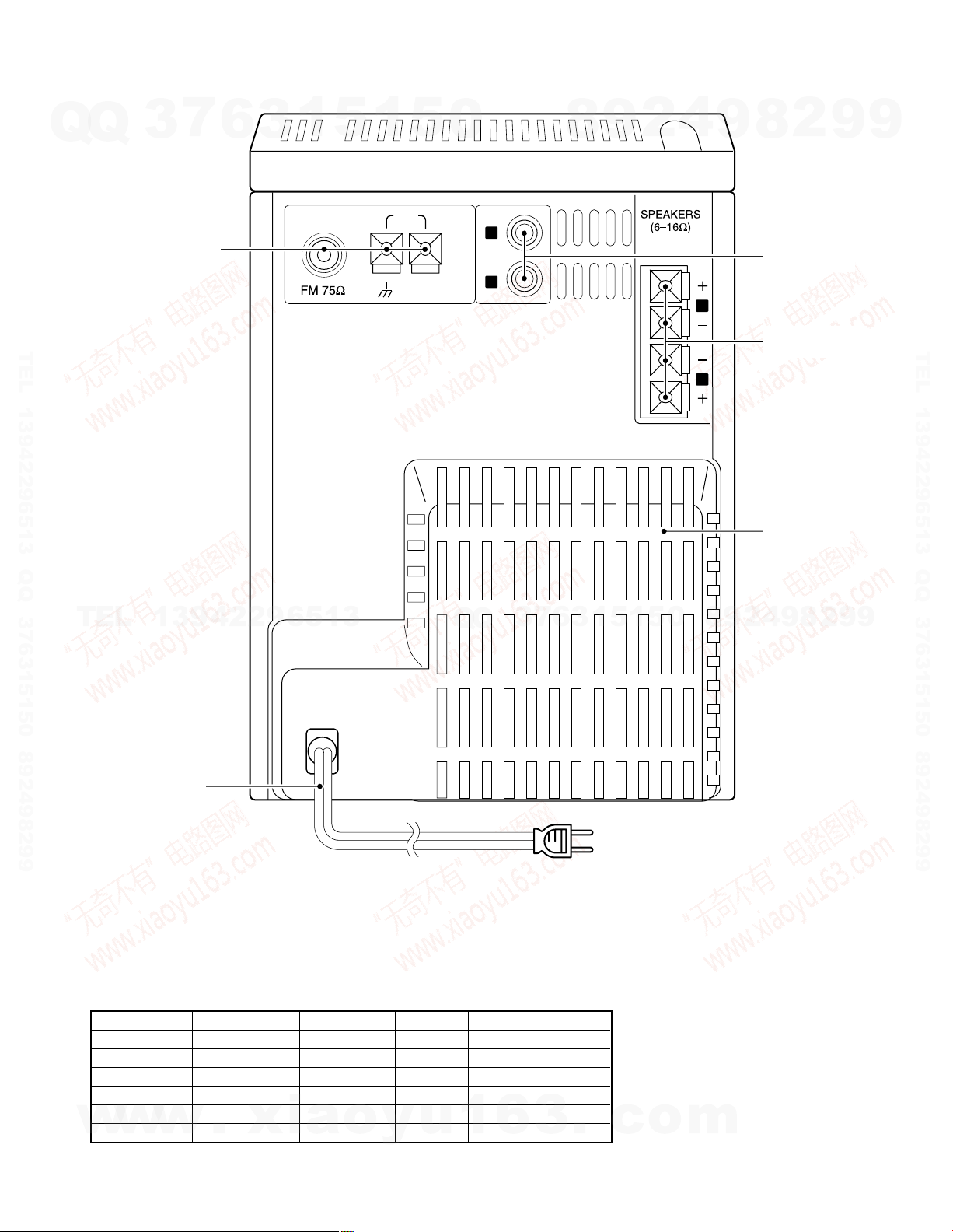
Door ass'y *
(F07-)
F. Cab. assy *
(A60-)
8
4
2
9
© 2002-12 PRINTED IN KOREA
B51-5813-00 (K/K) 3070
Button
(K29-8259-08)
9
2
8
FL filter
(B11-1567-08)
9
9
TEL 13942296513 QQ 376315150 892498299
TEL
* Refer to parts list on page 26 .
In compliance with Federal Regulations, following are reproduction of labels on, or inside the product relating to laser
product safety.
w
Caution : No connection of ground line if disassemble
13942296513
TOP VIEW
w
w
the unit. Please connect the ground line on
rear panel, PCBs, Chassis and some others.
.
xia
o
Button
(K29-8260-08)
Knob(VOLUME)
(K29-8258-08)
Cass. door lens *
(B10-)
y
u
4
2
9
8
0
5
1
5
1
3
6
7
3
Q
Q
3
.
c
o
m
KENWOOD Corp. certifies this equipment conforms to DHHS
Regulations No.21 CFR 1040. 10, Chapter 1, subchapter J.
DANGER : Laser radiation when open and interlock defeated.
1
6
AVOID DIRECT EXPOSURE TO BEAM.
9
8
2
9
9
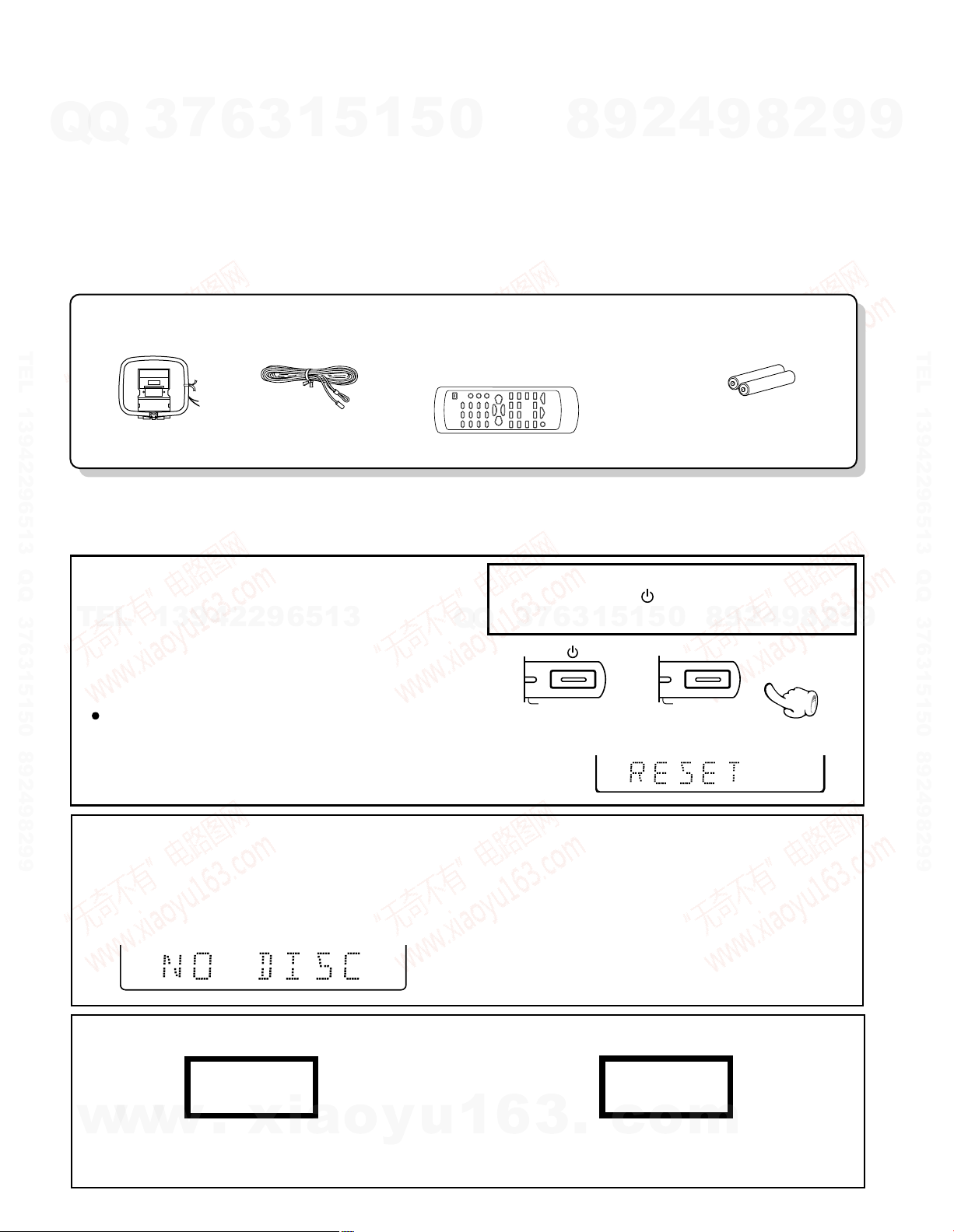
FM indoor antenna (1)
(T90-0861-08)
AM loop antenna (1)
(T90-0846-08)
Remote control unit (1)
(A70-1568-05): E,T,H type
(A70-1569-05): K,X type
Batteries(R6/AA) (2)
RXD-M35
Operation to reset
The microcomputer may fall into malfunction (impossibility to operate, erroneous display, etc.) when the power
cord is unplugged while unit is ON or due to an external
factor. In this case, execute the following procedure to
reset the microcomputer and return it to normal condition.
Unplug the power cord from the power outlet, then while
holding the POWER or
key depressed, plug the power
cord again.
Please note that resetting the microcomputer clears
the contents stored in and it returns to condition
when it left the factory.
or
After resetting the microcomputer, the display will show
as follow:
standby/ timer
POWER
The marking of products using lasers (For countries other than U.S.A., U.S.-Military and Canada)
The marking of this product has been classified as Class 1. It means
that there is no danger of hazardous radiation outside the product.
Location: Back panel
CLASS 1
LASER PRODUCT
CAUTION
VISIBLE LASER RADIATION
WHEN OPEN. DO NOT STARE
INTO BEAM OR VIEW DIRECTLY
WITH OPTICAL INSTRUMENTS.
Inside this laser product, a laser diode classified as Class 3A laser
radiation is contained as alerted by the internal caution label shown
above. Do not stare into beam or view directly with optical instruments.
1 Remove the CD from the unit.
2 Press the CD 6 key.
3 Wait for some time and verify that the display
appears as above.
4 Wait a few seconds and turn the unit OFF.
Note related to transportation and movement
Before transporting or moving this unit, carry out the following operations.
CONTENTS / ACCESSORIES / CAUTIONS
Contents
7
Q
Q
CONTENTS / ACCESSORIES / CAUTIONS............. 2
EXTERNAL VIEW .......................................................3
CIRCUIT DESCRIPTION ............................................4
ADJUSTMENT ..........................................................14
PC BOARD .............................................................. 15
Accessories
3
6
3
1
5
1
5
0
SCHEMATIC DIAGRAM .......................................... 19
EXPLODED VIEW ....................................................25
PARTS LIST..............................................................26
SPECIFICATIONS ......................................Back cover
8
9
2
9
8
4
2
9
9
TEL 13942296513 QQ 376315150 892498299
Cautions
TEL
13942296513
Q
3
Q
7
0
5
1
5
1
3
6
standby/ timer
8
9
2
4
9
8
2
9
TEL 13942296513 QQ 376315150 892498299
9
w
w
2
w
.
xia
o
y
u
1
6
3
.
c
o
m
EXTERNAL VIEW
ANTENNA
AM
AUX
IN
L
R
L
R
RXD-M35
7
Q
Q
TEL 13942296513 QQ 376315150 892498299
TEL
3
Speaker terminal
(E70-0112-08)
13942296513
6
3
1
5
1
5
0
Q
Q
3
7
8
6
3
9
1
5
1
2
5
4
0
9
8
8
RCA jack
(E63-1091-08)
Speaker terminal
(E70-0113-08)
Heatsink cover
(F07-1799-08)
4
2
9
2
9
8
9
2
9
9
TEL 13942296513 QQ 376315150 892498299
9
AC line cord *
(E30-)
SYSTEM CONFIGURATIONS
SYSTEM RECEIVER SPEAKERS COLOR FOR
HM-335-S RXD-M35-S LS-M35-S SILVER USA & AUSTRALIA
HM-335E-S RXD-M35E-S LS-M35-S SILVER
HM-F30-S RXD-M35-S LS-F30 SILVER FRENCH
HM-335IT-S RXD-M35-S LS-F30 SILVER ITALY
HM-335-N RXD-M35-N LS-M35-N GOLD
w
w
HM-335E-N RXD-M35E-N LS-M35-N GOLD
w
.
xia
o
y
u
1
6
3
* Refer to parts list on page26.
.
c
o
m
3
RXD-M35
CIRCUIT DESCRIPTION
7
1. Initializing
Q
Q
1-1 Initialization Method
1-2 Initialization Operation
2. Tuner Types
TEL 13942296513 QQ 376315150 892498299
E,T,H, E3 FM 87.5MHz~108.0MHz 50kHz +10.7MHz 25kHz
M,X,
M,V K2
Voltage (IC401, Pin3) 4.2V~5.0V 2.6V~4.1V 1.4V~2.5V 0.7V~1.3V
3
• While pressing the [POWER] key, turn the AC on.
• During the initial operation, the display shows
"RESET" and after that it will be returned to standby
condition.
• If any mechanisms error occurred, the error indication
is displayed as "ERR" in the display.
Set Destination Band Receiving Frequency Range
K,P K1
E2 RDS AM 531kHz~1602kHz 9kHz +450kHz 9kHz
V AM 531kHz~1602kHz 9kHz +450kHz 9kHz
Type E,E2,T,H K,P M,V X
6
E1
1
5
1
3
FM 87.5MHz~108.0MHz 100kHz +10.7MHz 25kHz
AM 530kHz~1700kHz 10kHz +450kHz 10kHz
FM 87.5MHz~108.0MHz 50kHz +10.7MHz 25kHz
FM 87.5MHz~108.0MHz 100kHz +10.7MHz 25kHz
AM 530kHz~1610kHz 10kHz +450kHz 10kHz
5
1-3 Mechanism Initializations
0
1CD Mechanism
• If a mechanism error occurred, the error indication is
displayed as "C ERR" in the display.
2Deck Mechanism
• If a mechanism error occurred, the error indication is
displayed as "X ERR" in the display.
8
9
Channel
Space
2
4
9
IF RF
8
2
9
9
TEL 13942296513 QQ 376315150 892498299
3. Tuner Preset Frequency
TEL
P.CH K1(K,P Type) E3(E,T,H,E2 Type) E1(M,X,V Type) K2(M,V Type)
1 FM 98.30MHz FM 98.30MHz FM 98.30MHz FM 98.30MHz
2 FM 108.0MHz FM 108.0MHz FM 108.0MHz FM 108.0MHz
3 FM 89.10MHz FM 89.10MHz FM 89.10MHz FM 89.10MHz
4 FM 87.50MHz FM 87.50MHz FM 87.50MHz FM 87.50MHz
5 FM 90.00MHz FM 90.00MHz FM 90.00MHz FM 90.00MHz
6 FM 87.50MHz FM 87.50MHz FM 87.50MHz FM 87.50MHz
7 FM 87.50MHz FM 87.50MHz FM 87.50MHz FM 87.50MHz
8 AM 1610kHz AM 1503kHz AM 1503kHz FM 87.50MHz
9 AM 1700kHz AM 1584kHz AM 1584kHz AM 1610kHz
10 AM 1000kHz AM 999kHz AM 999kHz AM 1000kHz
11 AM 630kHz AM 621kHz AM 621kHz AM 630kHz
12 AM 1440kHz AM 1350kHz AM 1350kHz AM 1440kHz
13 FM 106.0MHz FM 106.0MHz FM 106.0MHz FM 106.0MHz
14 AM 530kHz AM 531kHz AM 531kHz AM 530kHz
15 FM 87.50MHz FM 87.50MHz FM 87.50MHz FM 87.50MHz
16 FM 98.00MHz FM 98.00MHz FM 98.00MHz FM 98.00MHz
17 FM 98.50MHz FM 98.50MHz FM 98.50MHz FM 98.50MHz
18 FM 87.50MHz FM 87.50MHz FM 87.50MHz FM 87.50MHz
19 AM 990kHz AM 945kHz AM 945kHz AM 990kHz
20 FM 97.40MHz FM 97.40MHz FM 97.40MHz FM 97.40MHz
21 AM 530kHz AM 531kHz AM 531kHz AM 530kHz
22 FM 87.50MHz FM 87.50MHz FM 87.50MHz FM 87.50MHz
23 FM 87.50MHz FM 87.50MHz FM 87.50MHz FM 87.50MHz
24 FM 87.50MHz FM 87.50MHz FM 87.50MHz FM 87.50MHz
25 FM 87.50MHz FM 87.50MHz FM 87.50MHz FM 87.50MHz
26 FM 87.50MHz FM 87.50MHz FM 87.50MHz FM 87.50MHz
27 FM 87.50MHz FM 87.50MHz FM 87.50MHz FM 87.50MHz
w
28 FM 87.50MHz FM 87.50MHz FM 87.50MHz FM 87.50MHz
29 FM 87.50MHz FM 87.50MHz FM 87.50MHz FM 87.50MHz
4
30 FM 106.0MHz FM 106.0MHz FM 106.0MHz FM 106.0MHz
13942296513
w
w
.
xia
Frequency
o
y
u
Q
Q
1
3
6
7
3
6
3
.
1
1
5
c
0
5
o
9
8
m
2
4
9
8
2
9
9
CIRCUIT DESCRIPTION
RXD-M35
4. Test Mode
Q
Q
4-1 Setting method of the Test Mode
Test Mode Keys Setting Method
CD MODE CD PLAY key Insert the AC cord to AC wall
DECK MODE TAPE PLAY
4-2 Cancel of the test mode
• Initialized and cancel the test mode if pulling out the power cord.
• Cancel the test mode only if the power key is turned off.
4-3 Contents of the Test Mode
TEL 13942296513 QQ 376315150 892498299
• The muting during mode selection is not controlled in the test mode.
• During the test mode, it can be operated in a special manner that is different from an
ordinary operation by using the keys on the main body, specifically as shown in the
following tables
4-4 CD Test Mode
TEL
7
3
(Cyclically changed the mode (✽✽: ✽✽)Time Display • Pickup moves inward.
05 and 03 by pressing the key.) 03
(Cyclically changed in the 07 FG/FE FG value /FE value
13942296513
6
Keys Display Operation
CD-PLAY/PAUSE 05
CD STOP 00 : 00 Stop the CD operation.
stop mode only.) 08 FB/FO FBAL value /FO value
SKIP UP Ex.0.1~0.2 • Track number up
SKIP DOWN Ex.0.2~0.1 • Track number down.
3
1
5
1
5
outlet while holding down the
left key.
(✽✽: ✽✽)Time Display • Pickup moves outward.
0
✽✽: ✽✽
✽✽: ✽✽
09 TG/TE TG value /TE value
10 TB/TO TBAL value /TO value
Q
Q
3
7
4
2
9
8
• Tracking-servo on.
• Tracking-servo off. (for checking TE)
Adjustment value/mean value
8
0
5
1
5
1
3
6
9
9
8
2
4
2
9
8
9
2
9
9
TEL 13942296513 QQ 376315150 892498299
9
4-5 Deck Test Mode
Keys Display Operation
• 4 Seconds Recording
If the REC/ARM key is pressed, the system record for 4 seconds.
TAPE REC AUX
✽
Mechanism half switches indication
The mechanism half switches status are indicated "blank" or "E" in the display.
8th Dot(Display) 1st figure 2nd figure 3rd figure 4th figure
Mechanism FWD REC Inhibit RVS REC Inhibit Cassette Half Tape Play
Half Switch Detection SW Detection SW Detection SW Detection SW
ON Blank Blank Blank Blank
OFF E E E E
w
w
w
.
xia
Then, it rewinds to the REC starting position and plays back automatically.
If the REC/ARM key is pressed, during the 4 seconds REC operation, the
system records further for 4 seconds, then returns to the starting position
of the first 4 seconds REC operation and plays back.
o
y
u
1
6
3
.
c
o
m
5
RXD-M35
CIRCUIT DESCRIPTION
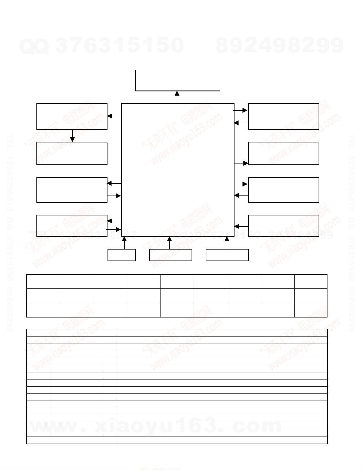
5. Microcomputer : MN101C51F (IC401)
Q
Q
5-1 Microcomputer Periphery Block Diagram
IC801
TEL 13942296513 QQ 376315150 892498299
FL801 IC301
Vaccume Fluorescent Display
IC202 IC102
7
3
FL DRIVER
(MN12510F)
(HNA-14SM06)
DSP IC
(MN662748WB)
6
3
1
5
1
5
IC701
PLAY BACK/REC EQ. IC
MN101C51F
0
AN7317
IC401
8
9
2
4
9
DECK MECHA.
SYSTEM IC
(LC75342M)
PLL IC
LC72131M
IC103
8
2
9
9
TEL 13942296513 QQ 376315150 892498299
CD MECHA.
(KSM213)
TEL
Key Matrix VREF =5.0V
Voltage
Range
Key 1 ON/
(Pin 5) STANDBY DOWN PLAY UP
Key 2
(Pin 6) PLAY
5-2 Pin Description of Microcomputer : MN101C51F (IC401)
Pin No. Pin Name I/O Description
1 VREF - - Connected to power supply(+5.0V).
2 END SW I Reel sensor input for cassette deck.
3 TN TYPE I Discrimination of tuner destination.
4 S LEVEL I RDS signal level input(E/T type only).
5 KEY1 I A/D key (key1) input port.
6 KEY2 I A/D key (key2) input port.
7 A LEVEL - Unused.
8 TH - Unused.
9 CD PROTECTION I Detection port for CD protection.
10 VREF + I A/D reference voltage(+5V).
11 VCC I Power supply(+5.0V).
12 OSC2 O Main clock oscillator(8.388MHz).
13 OSC1 I Main clock oscillator(8.388MHz).
w
14 VSS I GND.
15 X1 I Timer clock input(32.768kHz).
13942296513
0 0.89 1.55 2.00 2.61 3.02 3.42 5.00
REC
w
w
.
xia
7
3
Q
Q
IC802 VR801
KEY REMOTE ENCORD
u
SKIP
1
6
STOP
TAPE
3
AUX TUNER
o
y
6
3
.
0
5
1
5
1
CD SKIP
MODE SET (off)
c
o
RDS IC (E/T TYPE)
(BU1923F)
4
2
9
8
m
9
8
(off)
2
9
9
6

CIRCUIT DESCRIPTION
RXD-M35
Q
TEL 13942296513 QQ 376315150 892498299
Pin No. Pin Name I/O Description
Q
16 X0 O Timer clock output(32.768kHz).
17 MMOD - Connected to ground.
18 S DI I Data input from FL driver IC.
19 S.DO O Data output to FL driver IC.
20 S CK O Clock output to FL driver IC.
21 MLD O CD DSP command load signal output.
22 SUBQ I CD sub code input.
23 SQCK O Clock output for CD sub code.
24 CL SW I CD close detection switch input.
25 RESET I Reset signal input for microprocessor.
26 CE I Power failure input port.
27 OP SW I CD open detection switch input.
28 CD POWER O CD DSP power on/off control.
29 XRST O CD DSP reset output.
30 SLT SW I CD start limit switch input.
31 REM. CONTROL I Remote control signal input.
32 NO USE - Unused.
33 RDS CLK I RDS clock input. (E/T version only)
34 RESET2 - Unused.
35 CD BLKCK I Sub code synchronous signal input.
36 MDATA - Unused.
37 STAT I CD DSP status signal input.
38 MCLK O CD DSP command clock signal output.
39 CLOSE - Unused.
40 OPEN - Unused.
41 PH IN I Unused.
TEL
42 FLASH UC1 - Unused.
43 FLASH UC2 - Unused.
44 V CE O Chip enable output to electronic volume system IC.
45 V CLK O Clock output to electronic volume system IC.
46 V DATA O Serial data output to electronic volume system IC.
47 PWR RELAY O Power relay control output. H = ON L = OFF
48,49 NO USE - Unused.
50 FLASH WRITE - Unused.
51 NO USE - Unused.
52 PLL CLK O PLL IC clock output.
53 PLL DO/ST I PLL IC data input.
54 PLL DATA O Data output to PLL IC.
55 PLL CE O PLL IC chip enable.
56 SD I SD detector input. H = NO TUNED L = TUNED
57 TU MUTE O Tuner mute control. L : MUTE ON
58 PACK SW I Deck pack switch input. H = OFF L = ON
59 F REC SW I Deck forward rec switch input. H = OFF L = ON
60 R REC SW I Deck reverse rec switch input. H = OFF L = ON
61 PLAY SW I Deck play switch input. H =OFF L =ON
62 B. CANCEL - Unused.
63 REC/PB O Deck rec/play control.
64 BIAS O Deck bias control.
65 A/B O Unused.
66 LINE MUTE O Deck line mute control.
67 REC MUTE O Rec mute control.
68 CPM O Deck capstan motor control.
69 SOL O Deck solenoid control.
w
w
70 RDS DATA - Unused.
7
3
13942296513
w
6
.
xia
3
1
5
o
1
y
5
u
0
Q
Q
1
3
6
7
3
8
6
3
.
9
1
1
5
c
2
5
o
4
0
m
9
8
9
8
2
4
2
9
8
9
2
9
9
TEL 13942296513 QQ 376315150 892498299
9
7
RXD-M35
CIRCUIT DESCRIPTION
Pin No. Pin Name I/O Description
Q
Q
71 PROTECT O Detection input port for protection circuit H = PROTECTION ON
72 A_MUTE O Audio muting control output. H = OFF L = ON
73 SP. RERAY O Unused.
74 EEP SDA I/O EEPROM data input and output.
75 EEP SCL O EEPROM clock output.
76 ENC A I Rotary encoder input (up).
77 ENC B I Rotary encoder input (down).
78 LED. RED O Control port of standby/timer LED(red). L = ON
79 LED. GRN O Control port of standby/timer LED (yellow). L = ON
80 NCS O CS signal output to LCD driver IC.
TEL 13942296513 QQ 376315150 892498299
6. Pin Description of IC's
6-1 CD RF AMP : AN8399SA-E1 (IC201)
Pin No. Pin Name I/O Description
1 PD I APC Amp input.
2 LD O APC Amp output.
3 VCC - Power supply.
4 RF I RF amp inverting input.
5 RF OUT O RF addition amp output.
6 RF IN I AGC amp input.
7 LDRCTL - LD reference voltage control.
8 CAGC - AGC loop filter connection.
9 ARF O AGC output.
10 CEA - Capacitance connection for RF HPF-Amp.
11 RF ENV O 3T-ENV output.
TEL
12 CSBDO - Capacitance connection for RF dark side envelope detection.
13 BDO O BDO output.
14 COFTR - Capacitance connection for RF bright side envelope detection.
15 OFTR O OFTR output.
16 NRFDET O NRFDET output.
17 GND - GND
18 SLPSW - Sleep mode control (connected to ground).
19 VREF O VREF output.
20 TEN I TE. Amp inverting input.
21 TEOUT O TE. Amp output.
22 FEN I FE. Amp inverting input.
23 FEOUT O FE. Amp output.
24 GCTL O Gain & APC control.
25 FBAL O F. BAL control.
26 TBAL O T. BAL control.
27 E I Tracking signal input 1.
28 F I Tracking signal input 2.
29 D I Focus signal input 4.
30 B I Focus signal input 2.
31 C I Focus signal input 3.
32 A I Focus signal input 1.
7
3
13942296513
6
3
1
5
1
5
0
Q
Q
3
7
8
6
3
9
1
5
1
2
5
4
0
9
8
9
8
2
4
2
9
8
9
2
9
9
TEL 13942296513 QQ 376315150 892498299
9
8
w
w
w
.
xia
o
y
u
1
6
3
.
c
o
m
CIRCUIT DESCRIPTION
RXD-M35
6-2 DSP IC : MN6627482WB( IC202)
Q
Q
Pin No. Pin Name I/O Pin Description
1 BCLK O Bit clock output for SRDATA.
2 LRCK O L, R clock signal output.
3 SRDATA O Serial data output.
4 DVDD1 - Digital power supply.
5 DVSS1 - Digital ground.
6 TX O Digital audio interface signal output.
7 MCLK I CPC command clock signal input.
8 MDATA I CPU command data signal input.
9 MLD I CPU command load signal input. Load
TEL 13942296513 QQ 376315150 892498299
10 SENSE O Sense signal output(OFT, FESL, NACEND, NAJEND, SFG).
11 FLOCK O Focus servo signal output.
12 TLOCK O Tracking servo signal output.
13 BLKCK O Sub code block clock output. fBLKCK = 75Hz
14 SQCK I Sub code Q data clock input pin.
15 SUBQ O Sub code Q data signal output pin.
16 DMUTE I Connected to be ground. Mute
17 STAT O Status signal output.
18 XRST I Reset signal input. Reset
19 SMCK O
20 PMCK O
21 TRV O Traverse forced feed output.
22 TVD O Traverse drive output.
TEL
23 PC O Spindle motor on signal output. L : ON (Default)
24 ECM O Drive signal output for spindle motor (forced mode output).
25 ECS O Drive signal output for spindle motor (servo error signal output).
26 KICK O Kick pulse output for tracking driver.
27 TRD O Tracking servo drive output.
28 FOD O Focus drive output.
29 VREF I Reference power supply for DA output section.
30 FBAL O Focus balance adjusting output.
31 TBAL O Tracking balance adjusting output.
32 FE I Focus error signal input (analog input).
33 TE I Tracking error signal input (analog input).
34 RFENV I
35 VDET I/O
36 OFT I Off track signal input. Off Track
37 TRCRS I Track cross signal input pin (analog input).
38 RFDET I RF detector signal input pin. Detected
39 BDO I Drop out signal input. Drop Out
40 LDON O Laser on signal output. ON
41 PLLF2 I/O PLL loop filter switching pin.
42 TOFS O Tracking offset adjusting output.
43 WVEL O Double speed status signal output.
44 ARF I RF signal input.
45 IREF I Reference current input pin.
46 DRF I DSL bias pin.
w
w
47 DSLF I/O DSL loop filter pin.
48 PLLF I/O PLL loop filter pin.
49 VCOF I/O VCO loop filter pin.
7
3
13942296513
w
6
.
xia
1
3
8.4672MHz clock signal output when MSEL is H.
4.2336MHz clock signal output when MSEL is L.
88.2kHz clock signal output when default.
Play signal output when command is carry out.
RF envelope signal input (analog input).
Vibrating detection signal input when default.
Software vibrating detection monitor output when command is
executed.
5
o
1
y
5
u
0
Q
Q
1
3
6
7
3
8
6
3
.
9
1
1
5
c
2
5
o
4
0
m
9
8
9
2
Active
2
8
9
9
8
HL
Play
9
4
2
Detected
Double
Speed
9
TEL 13942296513 QQ 376315150 892498299
9
9
 Loading...