

Page 1
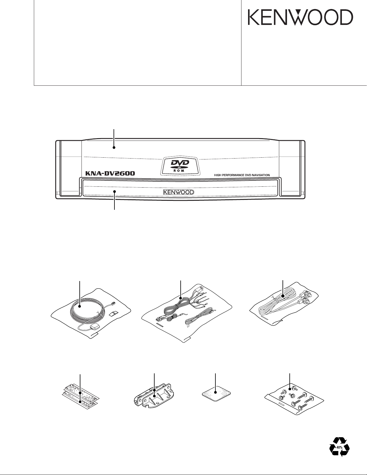
DVD NAVIGATION SYSTEM
KNA-DV2600
SERVICE MANUAL
Dressing panel assy
(A21-4353-02)
© 2003-12 PRINTED IN JAPAN
B53-0109-00 (N) 37
Dressing panel assy
(A21-4355-03)
Electric circuit module
(W02-3261-05)
Magic tape
(H30-0514-05) x2
DC cord assy
(E30-6334-05)
Bracket
(J19-4596-04) x2
Mounting hardware assy
(J21-9867-04)
Connecting cord assy
(E30-6199-05)
Screw set
(N99-1713-05)
Page 2
2
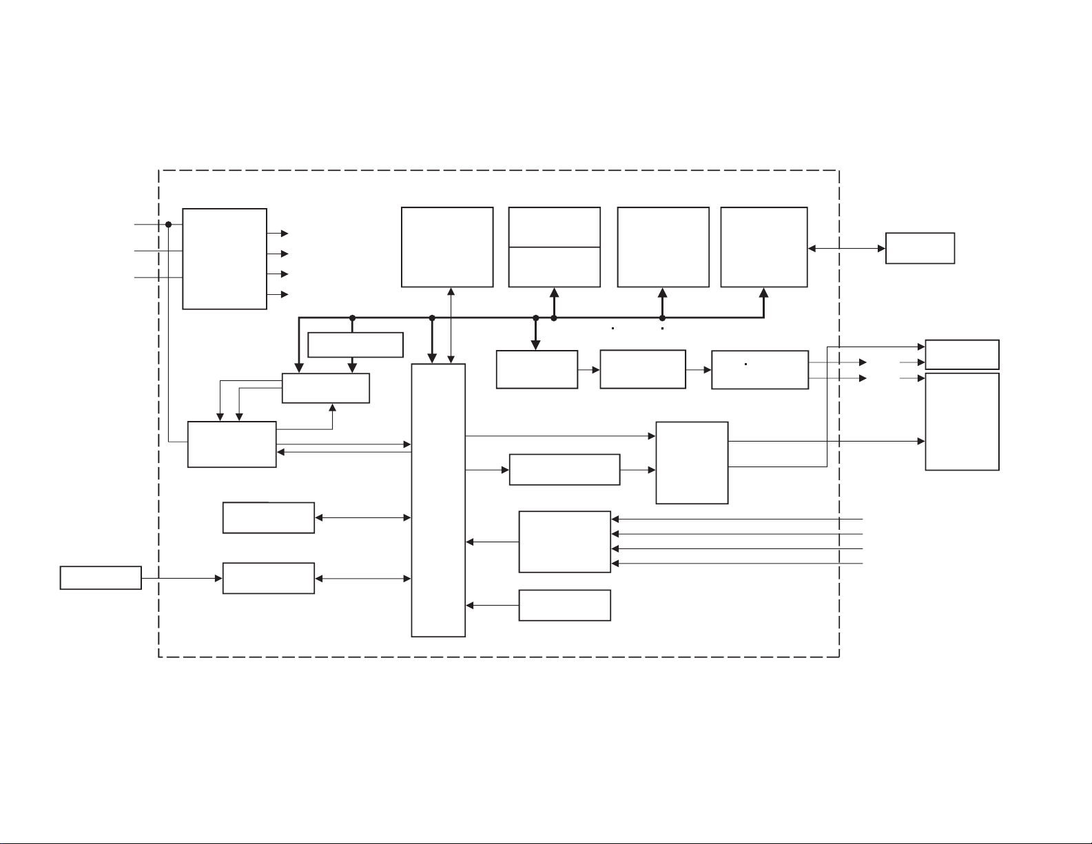
DVD
IC901,902
IC905 IC951-955,T951
IC906
MECHA.
CFC INTERFACE
POWER
SUPPLY
IC101,103,104,106,107
T101,104-111
6.7V DVD
5V
OUTSIDE INTERFACE
3.3V
INSIDE INTERFACE
1.8V
SH4
+B
ACC
GND
SDRAM
(16MBX2)
BOOTROM
(2MB)
SRAM
(512KB)
DATA ADDRESS CONTROL SIGNAL
FMU3
IC303 IC301 T507
T502-504,506,508
IC507
IC352,353
IC451,452
GY801
DAC&
NTSC ENCODER
VOICE REFLECTION
OUTPUT INTERFACE
SIGNAL CONTROL IC
IC202
IC201
STATUS0.1
SH4
T102,103
IC110
IC105
SHCKE
RESET
WDP
B.UP
NMI
IO
-PLUS
RS422
IC402,403
IC431-433,435,437
IC802,809,810
GPS MCM
GPS ANTENNA
GYRO
VEHICLE
INTERFACE
VOICE GUIDANCE,
VOICE OUTPUT CIRCUIT
MUTE
SWITCHING
INTERFACE
NAVI VOICE/BEEP
TV VOICE
PKB
REV
ILL
SPD
DISPLAY
REFLECTION
VOICE
MONITOR
NTSC
RGB
CFC
KNA-DV2600
BLOCK DIAGRAM
Page 3

KNA-DV2600
COMPONENTS DESCRIPTION
● MAIN UNIT
Ref No. Application/Function Operation/Condition/Compatibility
IC101 Switching regulator IC DC/DC Converter voltage controller for 6.8V and 3.3V power lines
IC103 AVR IC 3.3V output
IC104 AVR IC 5V output
IC105 Comparator ACC & BU voltage detector
IC106 AVR IC 1.8V output
IC107 Reset IC When momentary power down has detected, IC outputs “Lo”.
IC110 Reset MI-COM Reset controller for Main CPU and peripheral circuits
IC201 Main CPU (SH4)
IC202 Data controller Data selector of data bus
IC301 Video DAC+NTSC encoder
IC302 NAND Clock buffer
IC303 Graphics controller Graphics data generator (FMU III)
IC352 Op. Amp. Audio and beep signal adder and buffer
IC353 Analogue SW
IC357 AND Audio mute control signal generator
IC433~437 Inverter
IC438 AVR IC 3V output
IC452 Inverter Vehicle speed pulse waveform shaping
IC601 AVR IC For DVD mechanism
IC606 NAND DVD interrupt signal buffer (3V → 5V level converter)
IC653 DARC decoder FM multiple data demodulator
IC801 IO PULS Extended IO
IC802 Inverter
IC809 Inverter
IC810 Inverter
IC901,902 SDRAM 128M
IC903 AND SH-CKE buffer
IC904 NAND CSRAM buffer
IC905 BOOT ROM 2M
IC906 SRAM 256K
T101 PON SW While ACC is applied and IC110’s P37 is “Hi”, BU is supplied throu T101.
T102 PON SW While ACC is applied, T102 is turned on.
T103 PON SW When IC110's P37 becomes “Hi”, T103 is turned on.
T104 Driver T110 driver
T105,106 Driver T111 driver
T107 BVCC3D power supply selector T107 is turned on during BACKUP mode.
T108 BVCC3D power supply selector T108 is turned on except BACKUP mode.
T109 Driver T110 driver
T110 DC/DC chopper For 6.8V AVR
T111 DC/DC chopper For 3.3V AVR
T401
T402 When T402's base becomes “Hi”, T401 is turned on.
LMUTE driver
External LINE MUTE signal driver
● SUB UNIT
Ref No. Application/Function Operation/Condition/Compatibility
IC508 AND TV monitor's RX/TX signal buffer
IC510 Signal selector Remote control signal selector of TV and external remote sensor
T501 Audio mute SW For RCA pin jack
T502 Audio signal buffer For RCA pin jack
T505 TV audio signal mute SW For TV monitor
T506 TV audio signal buffer For TV monitor
T507 SYNC signal buffer For TV monitor
T508 Mute SW driver For audio signal muting
3
Page 4

KNA-DV2600
MICROCOMPUTER’S TERMINAL DESCRIPTION
● IC110 : MAIN UNIT (RESET MICROPROCESSOR)
Pin No. Pin Name I/O Description Processing Operation
1P04 (TEL-CGON) O Power supply circuit control output Hi : Power supply circuit ON
2 P05 (TEL-CHAG) I Power supply circuit ON request input Hi : Start request
3 P06 (ACC ON) O ACC ON output to IO PLUS Lo : ACC ON
4 P07 (B UP) O Backup condition set-up output Lo : Backup condition
5 MODE0 - Not used (connected to GND lines)
6 MODE1 - Not used (connected to GND lines)
7 RST I
8XOOResonator connection terminal
9XIIResonator connection terminal
10 VSS - GND connection terminal Connected to GND lines.
11 P37 (POWER ON) O P ON output Hi : Power ON
12 P36 (WDP) I WDP input Detection of pulse edge
13 P35 (ACC) I ACC detection input Hi : ACC ON
14 P34 (BU) I Momentary power down detection Hi : BU ON
15 P33 (CKE) I CKE from SH4
16 C - Capacitor connection terminal
17 P32 (IOPFLWR) O Not used (N.C.)
18 P31 (ST1) I Status input 1 from SH4
19 P30 (ST0) I Status input 0 from SH4
20 P50 (IORES) O IO PLUS reset output Lo : Reset
21 AVSS - GND connection terminal Connected to GND lines.
22 P40 (VCC3ON) O VCC3D selection terminal (Normal) Lo : Normal operation
23 P41 (BVC3ON) O VCC3D selection terminal (Backup) Lo : Backup mode
24 P42 (RMUTE) O Mute output at Power ON/OFF Lo : Mute ON
25 P43 (RES3) O NAVI reset output (VCC3 system reset signal) Lo : Reset
26 P00 (SH4NMI) O NMI output to SH4 Hi → Lo : Back up request to SH4
27 P01 (TEL-OVER) I Output voltage watch of power supply circuit Lo : Output imprudence
28 P02 (6.8VDET) I Output voltage watch of 6.8V power line (CDHVCC) Hi : Output voltage OK
29 P03 (3.3VDET) I Output voltage watch of 3.3V power line (VCC3) Hi : Output voltage OK
30 VCC - Positive power supply connection terminal Connected to Backup power supply.
RESET input (connected with RESET SW on the panel)
Lo : Reset
Lo : SDRAM self-refresh, Hi : SDRAM normal operation
● IC201 : MAIN UNIT (MAIN MICROPROCESSOR)
Pin No. Pin Name I/O Description Processing Operation
1RDY IRDY input
2 RESET I Reset input Lo : Reset
3CS0 O Chip select 0 output Lo : Selected (BOOT ROM)
4CS1 O Chip select 1 output Lo : Selected (SRAM)
5CS4 O Chip select 4 output Lo : Selected (IO PLUS)
6CS5 O Chip select 5 output Not used (N.C.)
4
Page 5

KNA-DV2600
MICROCOMPUTER’S TERMINAL DESCRIPTION
Pin No. Pin Name I/O Description Processing Operation
7CS6 O Chip select 6 output Lo : Selected (CF Card)
8BSOBus start
9 VDDQ - Positive power supply connection terminal (+3.3V) Connected to VCC3 lines.
10 VSSQ - GND connection terminal Connected to GND lines.
11 D47 I/O Data bus Not used (N.C.)
12 D32 I/O Data bus Not used (N.C.)
13 VDD - Positive power supply connection terminal (+1.8V) Connected to VCC1.8 lines.
14 VSS - GND connection terminal Connected to GND lines.
15 D46 I/O Data bus Not used (N.C.)
16 D33 I/O Data bus Not used (N.C.)
17 D45 I/O Data bus Not used (N.C.)
18 D34 I/O Data bus Not used (N.C.)
19 D44 I/O Data bus Not used (N.C.)
20 D35 I/O Data bus Not used (N.C.)
21 VDDQ - Positive power supply connection terminal (+3.3V) Connected to VCC3 lines.
22 VSSQ - GND connection terminal Connected to GND lines.
23 D43 I/O Data bus Not used (N.C.)
24 D36 I/O Data bus Not used (N.C.)
25 D42 I/O Data bus Not used (N.C.)
26 D37 I/O Data bus Not used (N.C.)
27 D41 I/O Data bus Not used (N.C.)
28 D38 I/O Data bus Not used (N.C.)
29 D40 I/O Data bus Not used (N.C.)
30 D39 I/O Data bus Not used (N.C.)
31 VDDQ - Positive power supply connection terminal (+3.3V) Connected to VCC3 lines.
32 VSSQ - GND connection terminal Connected to GND lines.
33 D15 I/O Data bus
34 D0 I/O Data bus
35 D14 I/O Data bus
36 D1 I/O Data bus
37 D13 I/O Data bus
38 D2 I/O Data bus
39 VDD - Positive power supply connection terminal (+1.8V) Connected to VCC1.8 lines.
40 VSS - GND connection terminal Connected to GND lines.
41 D12 I/O Data bus
42 D3 I/O Data bus
43 VDDQ - Positive power supply connection terminal (+3.3V) Connected to VCC3 lines.
44 VSSQ - GND connection terminal Connected to GND lines.
45 D11 I/O Data bus
46 D4 I/O Data bus
5
Page 6

KNA-DV2600
MICROCOMPUTER’S TERMINAL DESCRIPTION
Pin No. Pin Name I/O Description Processing Operation
47 D10 I/O Data bus
48 D5 I/O Data bus
49 D9 I/O Data bus
50 D6 I/O Data bus
51 BACK/BSREQ O Bus use permission output
52 BREQ/BSACK I Bus release request input
53 D8 I/O Data bus
54 D7 I/O Data bus
55 CKE O Clock enable
56 VDDQ - Positive power supply connection terminal (+3.3V) Connected to VCC3 lines.
57 VSSQ - GND connection terminal Connected to GND lines.
58 WE5/CAS5/DQM5 O Not used (N.C.)
59 WE4/CAS4/DQM4 O Not used (N.C.)
60 WE1/CAS1/DQM1 O D15~D0 choice output
61 WE0/CAS0/DQM0 O D15~D0 choice output
62~64 A17~A15 O Address bus
65 VDD - Positive power supply connection terminal (+1.8V) Connected to VCC1.8 lines.
66 VSS - GND connection terminal Connected to GND lines.
67,68 A14,A13 O Address bus
69 VDDQ - Positive power supply connection terminal (+3.3V) Connected to VCC3 lines.
70 VSSQ - GND connection terminal Connected to GND lines.
71~76 A12~A7 O Address bus
77 CKIO O Clock output
78 VDDQ - Positive power supply connection terminal (+3.3V) Connected to VCC3 lines.
79 VSSQ - GND connection terminal Connected to GND lines.
80~84 A6~A2 O Address bus
85,86 DRAK1,DRAK0 O Not used (N.C.)
87 VDDQ - Positive power supply connection terminal (+3.3V) Connected to VCC3 lines.
88 VSSQ - GND connection terminal Connected to GND lines.
89 CS3 O Chip select 3 output Lo : Selected (SDRAM)
90 CS2 O Chip select 2 output Not used (N.C.)
91 VDD - Positive power supply connection terminal (+1.8V) Connected to VCC1.8 lines.
92 VSS - GND connection terminal Connected to GND lines.
93 RAS O SDRAM RAS control output
94 RD/CASS/FRAME O SDRAM CAS control output
95 RD/WR O Read/Write control output
96
WE2/CAS2/DQM2/ICIORD
97
WE3/CAS3/DQM3/ICIOWR
98 WE6/CAS6/DQM6 O Not used (N.C.)
99 VDDQ - Positive power supply connection terminal (+3.3V) Connected to VCC3 lines.
O D31~D16 choice output
O D31~D16 choice output
6
Page 7

KNA-DV2600
MICROCOMPUTER’S TERMINAL DESCRIPTION
Pin No. Pin Name I/O Description Processing Operation
100 VSSQ - GND connection terminal Connected to GND lines.
101
WE7/CAS7/DQM7/REG
102 D23 I/O Data bus
103 D24 I/O Data bus
104 D22 I/O Data bus
105 RXD I Not used (N.C.)
106,107 DREQ0,DREQ1 I Not used (pull up to VCC3 lines)
108 D25 I/O Data bus
109 D21 I/O Data bus
110 D26 I/O Data bus
111 D20 I/O Data bus
112 D27 I/O Data bus
113 VDDQ - Positive power supply connection terminal (+3.3V) Connected to VCC3 lines.
114 VSSQ - GND connection terminal Connected to GND lines.
115 D19 I/O Data bus
116 D28 I/O Data bus
117 VDD - Positive power supply connection terminal (+1.8V) Connected to VCC1.8 lines.
118 VSS - GND connection terminal Connected to GND lines.
119 D18 I/O Data bus
120 D29 I/O Data bus
121 D17 I/O Data bus
122 D30 I/O Data bus
123 D16 I/O Data bus
124 D31 I/O Data bus
125 VDDQ - Positive power supply connection terminal (+3.3V) Connected to VCC3 lines.
126 VSSQ - GND connection terminal Connected to GND lines.
127 D55 I/O Data bus Not used (N.C.)
128 D56 I/O Data bus Not used (N.C.)
129 D54 I/O Data bus Not used (N.C.)
130 D57 I/O Data bus Not used (N.C.)
131 D53 I/O Data bus Not used (N.C.)
132 D58 I/O Data bus Not used (N.C.)
133 D52 I/O Data bus Not used (N.C.)
134 D59 I/O Data bus Not used (N.C.)
135 VDDQ - Positive power supply connection terminal (+3.3V) Connected to VCC3 lines.
136 VSSQ - GND connection terminal Connected to GND lines.
137 D51 I/O Data bus Not used (N.C.)
138 D60 I/O Data bus Not used (N.C.)
139 D50 I/O Data bus Not used (N.C.)
140 D61 I/O Data bus Not used (N.C.)
O Not used (N.C.)
7
Page 8

KNA-DV2600
MICROCOMPUTER’S TERMINAL DESCRIPTION
Pin No. Pin Name I/O Description Processing Operation
141 D49 I/O Data bus Not used (N.C.)
142 D62 I/O Data bus Not used (N.C.)
143 VDD - Positive power supply connection terminal (+1.8V) Connected to VCC1.8 lines.
144 VSS - GND connection terminal Connected to GND lines.
145 D48 I/O Data bus Not used (N.C.)
146 D63 I/O Data bus Not used (N.C.)
147 VDDQ - Positive power supply connection terminal (+3.3V) Connected to VCC3 lines.
148 VSSQ - GND connection terminal Connected to GND lines.
149 MD0/SCK I/O Clock movement matter mode selection terminal Pull up to VCC3 Lines.
150 MD1/TXD2 I/O
151 MD2/RXD2 I
152 IRL0 I Interrupt input 0
153 IRL1 I Interrupt input 1
154 IRL2 I Interrupt input 2
155 IRL3 I Interrupt input 3
156 NMl I NMl interrupt input
157 XTAL2 O Not used (N.C.)
158 EXTAL2 I Not used (connected to VCC3 lines)
159 VSS • RTC - GND connection terminal Connected to GND lines.
160 VDD • RTC (3.3V) - Positive power supply connection terminal (+3.3V) Connected to VCC3 lines.
161 RESERVED I Not used (connected to VCC3 lines)
162 VSS - GND connection terminal Connected to GND lines.
163 VDDQ - Positive power supply connection terminal (+3.3V) Connected to VCC3 lines.
164 CTS2 I/O Not used (pull up to VCC3 lines)
165 TCLK I/O Not used (pull up to VCC3 lines)
166 MD8/RST2 I/O Crystal resonator settlement terminal Pull up to VCC3 lines.
167 MD7/TXD I/O Master mode settlement terminal Pull up to VCC3 lines.
168 SCK2/MRESET I Not used (pull up to VCC3 lines)
169 VDD - Positive power supply connection terminal (+1.8V) Connected to VCC1.8 lines.
170 VSS - GND connection terminal Connected to GND lines.
171~176 A18~A23 O Address bus
177 VDDQ - Positive power supply connection terminal (+3.3V) Connected to VCC3 lines.
178 VSSQ - GND connection terminal Connected to GND lines.
179,180 A24,A25 O Address bus
181 MD3/CE2A I/O Area 0 bus width settlement terminal Pull down to GND lines.
182 MD4/CE2B I/O Area 0 bus width settlement terminal Pull up to VCC3 lines.
183 MD5/RAS2 I/O Pull down to GND lines.
184 DACK0 O Not used (N.C.)
Clock movement matter mode selection Pull up to VCC3 Lines/Communication output to
terminal/Communication output to TV monitor TV monitor
Clock movement matter mode selection Pull up to VCC3 Lines/Communication input from
terminal/Communication input from TV monitor TV monitor
8
Page 9

KNA-DV2600
MICROCOMPUTER’S TERMINAL DESCRIPTION
Pin No. Pin Name I/O Description Processing Operation
185 DACK1 O Not used (N.C.)
186 A0 O Address bus Not used (N.C.)
187 VDDQ - Positive power supply connection terminal (+3.3V) Connected to VCC3 lines.
188 VSSQ - GND connection terminal Connected to GND lines.
189 A1 O Address bus
190
STATUS0
191
STATUS1
192 MD6/IOIS16 I Area 0 bus normal settlement terminal Pull up to VCC3 lines.
193
ASEBRK/BRKACK
194 TDO O Data output terminal (UDI) Connected to the test pin (CN150).
195 VDD - Positive power supply connection terminal (+3.3V) Connected to VCC3 lines.
196 VSS - GND connection terminal Connected to GND lines.
197 TMS I Mode selection input terminal (UDI) Connected to the test pin (CN150).
198 TCK I Serial clock input terminal (UDl) Connected to the test pin (CN150).
199 TDI I Data input terminal (UDl) Connected to the test pin (CN150).
200 TRST I Reset input terminal (UDl) Connected to the test pin (CN150).
201 VDD-PLL2 - PLL2 positive power supply connection terminal Connected up to VCC3 lines.
202 VSS-PLL2 - GND connection terminal Connected to GND lines.
203 VDD-PLL1 - PLL1 positive power supply connection terminal Connected up to VCC3 lines.
204 VSS-PLL1 - GND connection terminal Connected to GND lines.
205 VDD-CPG - PG positive power supply connection terminal Connected up to VCC3 lines.
206 VSS-CPG - GND connection terminal Connected to GND lines.
207 XTAL I Crystal resonator connection terminal Frequency : 19.8MHz
208 EXTAL O Crystal resonator connection terminal
O CPU status output 0
O CPU status output 1
I/O Emulator special terminal (UDI) Connected to the test pin (CN150).
9
Page 10

KNA-DV2600
TEST MODE
Preparation: Connect the DVD Navigation system to TV monitor type of the KENWOOD touch panel.
1. How to enter the TEST mode.
(1) Touch upon the “Menu” on the TV monitor and switch to
the Navigation Menu screen.
(2) Touch the Area 1 and 2 on the Navigation menu screen in
the following order : 1 → 2 → 1 → 2 → 1 → 2.
(3) Switching the screen display on the Diagnosis Menu.
2. How to exit from TEST mode.
Reset the Navigation system by pressing the reset button on
the front panel
3. Items on the TEST mode.
By doing the following, various information can be obtained
from the Diagnosis Menu.
3-1 GPS information
The GPS reception status can be confirmed by touching on
the “GPS Information”.
When confirming on the GPS reception status, put up the GPS
antenna at a location where nothing blocks GPS reception.
If the almanac data is lost due to conducting repair work and
the like, the data can be rewritten by receiving GPS information with the GPS antenna, while the vehicle is stationary for
about 20 minutes.
(1) Elv./Azm : Displays current position of GPS in elevation
and azimuthally projected direction.
(2) Level : The reception level from each satellite is displayed
in values (C/N).
(3) Status : Displa ys whether receiving or in use. When in use,
it is used for measurements.
(4) Measurement Status : Displays - -/NG/2D/3D.
(5) Date : Displays current time and date.
(6) Position : Displays longitude and latitude of the current
position.
3-2 Vehic le Sensors
By touching the “Vehicle Signal”, the vehicle and gyro signals
can be confirmed.
• Vehicle Section
(1) Battery : On/Off.
(2) REV : Turned on when the gear is in Reverse.
(3) Number of SPD pulses : Indicated the number of ve-
hicle speed pulses. (Speed is indicated in two ways.)
• Gyro Section
The following values in (1) and (2) belo w are changed when
the ECU is rotated.
(1) Voltage : Displays the current gyro voltage.
(2) Relative direction : Displays the current relative direction.
3-3 Color bar Check
By touching the “Color bar check”, RGB condition of monitor
can be confirmed.
Whether set color matches the display color or not can be
confirmed.
3-4 Parts information
By touching the “Parts Information”, current NAVI and Disc
information can be confirmed.
• NAVI Information
Current navigation software and ROM used can be confirmed.
• Disc Information
Current format and data versions can be confirmed.
3-5 SRAM clear
Touch the “SRAM clear” more than 5 second on the display
when you need clearer data for SRAM memory.
10
Page 11

Navigation TEST Mode is operated as follows.
1
TEST MODE
3. TEST mode menu
Navigation Check
1
2 1 2 1
2
GPS Information
KNA-DV2600
Back
Parts Information
2
3-1. GPS information
GPS INFORMATION
Ensure nothing is blocking GPS reception
Elv Azm Level status Elv Azm Level status
73 /021 12 P
52 /183 58 P
32 /219 39 P
49 /097 20 T
Measurement
status
DateGMT 05/27/200009:46
80 /279 54 P
27 /121 26
19 /330 11
Latitude Longitude
39 59.0' 137 00.0'
Navi menu
Back
Vehicle Sensors
Color Bar Check
3-3. Color Bar Check
Navigation Color Bar Check
Need to confirm if the set color
matches the display color
3-4. Parts Information
Parts Information
Navi Information
Disc Information
Black
DENSO
0BD1
DENSO
V01.01.47
SRAM Clear
Red Green
Navi Menu
Blue White
Navi Menu
3-2. Vehicle Sensors
Vehicle Sensors
Vahicle Signal Battery
REV
SPD Pulse Count
Speed
Sensor Signal GYRO 2500mV
Relative bearing 359.0
Navi menu
ON
OFF
9999 Puls
75 mph
120km/h
3-5. SRAM Clear
degrees
11
Page 12

A B C D E
1
36
KNA-DV2600
1
PC BOARD (COMPONENT SIDE VIEW)
MAIN UNIT
CN110
10
85
53
256
5
R423
R422
R368
R362
IC606
R234
R235
104
192
1
25
50
C413
33
16
R243
X202
32
17
R246
25
36
R852
8
9
R363
4
5
6
1
C409
R605
R373
R374
24
IC202
37
R845
14 8
R430
IC402
R364
R359
R358
R354
R829
R836
C603
3
CN140
2
1
BA101
D602
6
7
16
G
R155 R154
5
4
3
IC651
C144
IC104
SW801
8
E
4
IC807
R857
R856
R858
1
R637
85
3
4
5
6
1
O
I
1
2
3
2
C
1
IC106
CN310
G
148514
C658
IC652
GY801
2
Z651
C145
T107
T108
IC808
R859
R806
C148
15
C151
R160
R159
23
33
E
B
R805
C107
O
I
22
E
B
34
C152
C801
CN100
D
R122
R124
R125
R121
15
R654
24
IC952
14 8
16 9
IC955
1
7
D101
D105
T101
X101
IC110
IC653
X651
IC101
16 9
C124
44
12
O
I
IC103
G
C106
14
85
IC105
S
D
G
R114
R109
18
C104
IC107
G
I
O
1
C123
3016
C209
C208
11
X201
1
R653
R654
1
IC904
1
IC953
4825
124
IC951
4825
T951
E
7
B
1
4
1
IC954
85
18
6
10
L101
C119
T110
R223
R129
R130
R221
R222
R226
R212
R211
R210
IC903
54
R908
54
24
C101
R227
R230
R208
R909
1
13 3
L103
S
G
C462
R454
R451
208 157
6
12
C458
C135
C118
SW451
C460
1
7
C408 R406
R472
14
IC452
8
1
IC451
9
48
49
R363
16
R367
R361
IC355
64
1
60
CN330
59
C229
105
D
156
T111
L102
S
G
C227
IC201
1
52
127
IC902
5428
1
IC906
4825
54 28
127
193
IC901
C804
CN340
1
26
IC403
3
1
R370
R369
13
48
IC801
R828
R827
R413
7
1
1
16
C369
12
1
1
R604
R826
48 25
R412
R415
R419
R425
R424
2
1
C372
R825
5
8
X351
R821
10
5
R386
157
208
R418
IC401
14
85
R822
R853
R408
T702
156
1
R823
6
1
C411
C713
T701
E
B
4
1
IC353
22
14
IC352
85
D802
129
128
65
64
C807
IC905 IC907
CN120
E
B
CN320
C302
IC303
C720
13
24
45
5
4
5
4
IC802 IC809 IC810
24
1
19
20
4
R304
12
IC301
25
R864
R863
R860
X801
R854
R813
C703
136
IC701
1
R303
1
C711
R302
7
12
Page 13

JIHGF
R304
1
24
6
4
5
4
5
4
5
4
KNA-DV2600
1
20
C720
12
IC301
25
R864
R863
R860
R854
R813
19
X801
C703
3
1
IC701
1
R303
1
C711
R302
1
36
R901
R902
R301
3
1
3
1
3
1
C712
R711
R727
R738
R737
48
37
R865 R867
R861
C825
C710
R710
R725
IC706
4
5
C318
52
C868
R866
R862
IC806
4
5
4
5
C305
IC302
105
1
IC804
4
5
RES
C709
R716
R729
IC705
104
53
C838
C837
C812
R869
R819
TXD
C706
C702
R703
R701
R728
C722
3
C724
1
24
13
25
C725
36
3
1
X802
17
148
D803
3
4
5
1
RXDENGND
1
2
C717
R702
C721
37
1
CN350
45
IC601
L801
C840
C841
1
R820
3
1
C701
IC702
85
5
8
IC703
13
12
1
48
R733
C608
IC805
CN130
4
1
4
1
IC704
1
15
20
3
14
21
C433 C436
R433
3
4
5
1
IC435
C439
R436
IC433
1
CN150
10
CN400
IC431
C435
4
5
C441
R438
IC437
45
R434
C434
2
3
3
1
IC432
C442
C438
28
C432
C431
C401
IC438
MAIN UNIT
IC T Address
101 4B
103 3C
104 4B
105 3C
106 6B
107 4C
3
1
110 4B
201 4D
202 4D
301 3F
7
6
302 4F
303 4E
352 3E
353 3E
401 2E
1
1
4
402 2D
431 3G
432 4G
433 4G
435 4G
437 2G
438 5G
451 2D
452 2D
601 5F
I
G
O
606 4D
651 3B
652 4B
653 5B
801 6E
802 6E
804 6F
809 5E
810 5E
901 6D
902 5C
903 5C
904 5C
905 6E
906 6C
101 3B
107 5B
108 5B
110 3C
111 3C
Refer to the schematic diagram for the values of resistors and capacitors.
2
3
4
5
6
7
13
Page 14

K L M N O
0
2
4
2
2
KNA-DV2600
1
PC BOARD (FOIL SIDE VIEW)
MAIN UNIT
C708
R705
R718
R709
R722
R724
R306
R310
TP303
C324
C306
TP702
C322
TP807
TP806
TP805
C822
C820
C716
R712
R720
R713
R726
R715
C303
C307
C836
C835
C834
R911
R910
13
C310
R706
R707
C718
IC357
TP304
TP804
C704
R714
TP701
R380R305
C304
R307
C373
C321
C814
C705
C719
R439
C723
54
TP302
D401
D402
C352
R351
R352
R353
R308
C320
TP301
TP205
C829
C827
C826
C823
C821
C819
C813
C811
C810
C404
C402
R731
TP204
R401
R732
R405
R404
C358
R356
TP353
R360
C319
13
IC203
C308C309
C833
R830
R831
C817
C816
C405
C406
R403
R849
R814
C809
R357
R365
R366
C316
C314
C312
C237
R247
C925
C933
C415
TP354
C604
5
4
R250
R249
R832
R833
R834
R815
R812
R811
R870
R402
C403
C401
C407
R407
R421
R420
R417
R416
C831
C357
C356
C364
C365
R242
C231
C808
R410
R409
R428C412
R414
R429 C414
D405
D403
TP351
R623
R622
C602
C230
C232
C805 C830
R835
R837
R841
R840
R842
R847
R843
R839
R844
R838
C806
TP201
TP803
C362
C353
C351
D406
C224
C220
C217
C214
C210
C234
R244
C832
C828
R970R982
R969
R959
C410
R426
R466
R471
R470
C824
R816
C818
C815
R980
R967
R468
C464
R464
R469
C125
TP202
R229
TP203
C203C204
R965
C461
TP108
R134
T105
B
E
C906
C905
C904
C902
R981
D108
R149
R144
C103
C120
D112
D201
D202
R217
R978
R459
R15
R135
T106
B
E
R14
C11
C12
C226
C20
R964
R963
R956
R955
R952
R463
R467
R465
R473
R462
C459
C127
C228
R238
C205
C909
R951
R966
R957
R958
R968
C907
R735
D701
R708
R719
R704
R717
R723
C715C707
T703
B
E
B
EB
T705
C714
2
C440
C445
R437
TP433
TP704
D702
R736
R721
TP703
E
T704
3
TP436
C435
R431
C444
R203
TP432
R432
TP437
TP601
C605
C606
C607
R602
4
C443
TP431
L403
L402
C446C437
5
TP435
R309
C317
C315
C313
C311
6
R206
D801
R817
R818
R848
R824
R850R846
7
14
Page 15

TSRQP
3
KNA-DV2600
1
C463
R458
R457
R461
64
R468
69
R459
61
R455
R475
D453
TP102
D451
C153
R147
R132
T109T104
B
E
R137
C150
R115
TP110
R906
R907
C922
C211
R207
R206
C154
TP130
R102
C111
R118
R138
C117
R166
R165
R170
R168
TP122
C653
TP107
C105
R110
R113
R120
R119
TP131
TP127
R101
C112
R116
R117
TP117
TP115
TP654
TP653
TP652
R111
R112
R123
R128
R107
C652
C654
TP105
R104
TP116
TP114
D108
C120
D112
4
5
144
103
D201
D202
R217
3
6
5
R150R149
R135
T106
B
E
R142
C114
C122
C202
C225C226
R219
R216
R214
R228
R231
R241
R220
R236
R240
C201
R105
TP109
C213
R146
C121
D113
R131
B
E
R139
C223
C219
C218
C911
C910
R460
R456
D104
C126
C110
R127
TP113
R656
R655
C657
C656
TP103
R108
C102
B
E
T103
TP111
R169
TP124
R164
R474
R411
TP101
TP104
R106
TP123
TP118
TP655
C662
C659
C665
C655
R161
R162
R156
D404
R103
D103
D109
TP106
B
E
C661
TP656
R803
R802
B
E
B
E
R148
C663
C664
T102
T402
T401
T651
B
E
TP128
C660
C651
TP112
R809
C803
R810
R855
R808
C802
R807
TP651
R801
R804
MAIN UNIT
IC T Address
357 3N
102 3Q
103 3Q
104 3P
105 3O
106 3P
109 3P
401 2Q
402 2Q
651 3Q
2
3
4
5
4
2
R978
1
R964
R963
R956
R955
R952
R961
R962
R960
R954
R953
C934
C924
C977
C976
C955
C953
R972
C951
C954
C952
R973
R971
TP120
TP119
C147
R152
D106
D117
TP121
R151
C612
R636
D107
6
R158
D601
7
Refer to the schematic diagram for the values of resistors and capacitors.
15
Page 16

U V W X Y
KNA-DV2600
1
2
3
4
5
6
PC BOARD
(COMPONENT SIDE VIEW)
SUB UNIT (A/2)
CN240
4
5
C541
IC506
13
5
R547
C515
4
C512
4
4
3
3
3
1
R525
R527
1
2
5
3
4
C511
1
C513
CN230
4
CN220
CN210
2
2
2
SUB UNIT
IC T Address
508 5U
2
510 5U
501 5U
(B/2)
R536
SW601
13
12
CN200
8
C559
D506
4
C558
D505
SW602
IC502
IC510
2
22
C528
C534
R508
R571
1
4
R503
8
1
C518
CN321
C555
IC504
14
1
C554
R565
5
4
R520
C530
C533
8
1
C557
C556
IC508
T501
BE
R564
R570
D507
1
85
21
IC507
5
4
8
5
8
7
C552
C553
R563
R569
C560
C531
IC501
14
8
IC503
1
C524
6
1
C562
R567
8
IC505
1
D503
R552
9
1
5
5
4
5
1
CN311
(FOIL SIDE VIEW)
SUB UNIT (A/2)
TP502
R509R516
C505
TP501
C519
C536
R506
EB
R548
R551
R545
R550
C502
TP505
R538
R554
R556
C550
R515
R549
T503
TP510
R546
R544
C543
C539
C538
R539
R559
C545
EB
R532
R533
R572
R573
R511
C521
R540
TP503
TP504
SUB UNIT
TP509
C508
TP507
T Address
502 5Y
505 6Y
R505
506 6X
R504
507 5Y
508 6Y
R568
R562
C551
C501
R541
C537
T506
T507
TP506
R561
R566
C506
C509
R543
EB
(B/2)
R633
C610
1
C609
R634
3
R553
C546
R574
T508
C504
R537
R557
C561
C507
T505
C548
R528
T504
C503
C517
C535
C544
C529
C510
EB
R518
EB
R502
C542
R555
R530
EB
R510
R531
R526
T502
R524
R501
R519
C522
TP511
TP508
R558
R560
D504
D502
C532
C514
EB
R523
C527
R517
R513
D501
R512
TP512
C547
C549
R514
R521
C520
7
Refer to the schematic diagram for the values of resistors and capacitors.
16
Page 17

A B C D E
D
V
KNA-DV2600
CN320
GREEN
SYNC
NTSC
DISPTX
DISPRX
REMO
AUDOUT
MUTE
AUDIN0
PTTSW
CDHVCC
CDHVCC
RED
BLUE
GND
GND
GND
GND
GND
VCC
VCC
NC
MAIN UNIT
1
2
3
4
5
6
7
8
TV-TX
9
TV-RX
10
11
12
13
TP353
14
15
16
17
18
19
20
21
22
R380
5.0V
6.8V
IC
100K
C
RED
(SUB UNITA/2)
CN200
8765
1 VIDEO
2 VDGND
4 AUDGND
3 AUDIO
CN210
13
101112 9
C501
2200P
1234
220P
C510
C550
C506
2200P
TV MUTE SW
TP506
100P
C552
100P
C553
R565
100P
C554
22K
R510
R536
R517
22K
C507
75 220u6.3
100P
R566
TP505
4.7K
4.7K
4.7K
4.7K
R563
62
100u6.3
10K
R569
R564
62
100u6.3
10K
R570
C560
100u6.3
62
10K
R571
IC508(3/4)
8
470
470P
220P
C520
C556R561
SYNC BUFFER
+
10K
D503
R541
330
T505
R543
22K
R582
R562
47P
C551
330 1
T501
R508
22K
R580
C558
C559
+
4
5
IC508
(2/4)
C537
22K
AUDIO BUFFERAUDIO MUTE SW
C514R503
22K
R518
10
9
1
R568
T507
+
D505D506
+
D507
22K
R552
6
RX
BUFFER
3.9K
C561
R573
TV BUFFER
T506
1K
R548
C557
220u6.362
10K
T502
1K
R514
R526
22K
4.7K
R525
TX
BUFFER
22P
22K
R551
+
22K
R521
C527
4.7K
VCC
R572
R574
150
0
10K
D504
VCC
VCC VCCVCC
IC510
5
A
5.0V
6
CH1
7
CH0
8
VDD
C528
0.01
1000P
R527
22K
VCC VCC
T508
10K
MUTE DRIVER
5.0V
VCC
REMO.SIGNAL
SELECTOR
1
2
GND
COM
CN321
RED
1
GREEN
2
BLUE
5.0V5.0V
TP508
3
4
5
6
7
8
9
10
11
12
13
14
15
16
17
18
19
20
21
22
GND
SYNC
GND
NTSC
GND
DISPTX
DISPRX
REMO
GND
AUDOUT
MUTE
AUDIN0
AUDIN1
GND
PTTSW
VCC
VCC
CDHVCC
CDHVCC
TP512
TP509
TP510
3.3
R567
R515
C521
1000P
22K
REMO.SIGNAL
BUFFER
VCCVCC
C555
47u16
+
C509
R511
220P
22K
TP511
4
3
VEE
2
INH
1
7
13
3
11
12
14
IC508(4/4)IC508(1/4)
1
TV I/F
(MONITOR)
CN200
1
DGND
2
(NC)
3
4
2
5
6
7
8
9
10
11
12
13
TV-REMO
GREEN
VGND
AGND
TV-R
BLUE
TV-TX
TV-RX
TV-L
SYNC
3
4
5
SUB UNIT A/2
IC508 : TC74VHCT08AF
IC510 : TC7W53FU
T501,505 : DTC143EK
T502,506 : 2SC2712
T507 : 2SA1162
T508 : RN1402
D503-507 : RD5.6S
6
MAINUNIT
IC101 : BA9743AFV
IC103 : SCI7810YTA
IC104 : BA05FP
IC105 : TC75W56FU
IC106 : PQ07VZ012ZP
IC107 : SCI7720YFA
IC110 : KKQ34F
IC202 : KKQ28F
IC301 : CXA2106R
IC302,904 : TC7SH00F
IC303 : KKQ22F
IC352 : UPC842G2
IC353 : TC7W53FU
IC357 : TC7SET08F
IC401 : CA0008AM
IC402 : SN65C1168NS
IC433,435,437,802,809,810
IC451 : TD62604F
IC452 : TC7WU04FU
IC601 : BA05FP
IC606 : TC7SET00F
IC652 : BA08FP
IC801 : KKQ35F
IC901,902 : HY57V1291620LT
IC905 : KKQ36F
IC906 : TC55V400FT70
HD6417750F167I:IC201
: TC7SU04F
UPC29L03T:IC438
LC72708EHS
:IC653
TC7SH08FIC903 :
T101,110,111 : 2SJ327Z
T102,103 : RN1404
T104,105 : 2SD1782K
T106,109 : 2SB1198K
T107 : 2SA1162
T108
T401 : RN2402
T402,651 : RN1402
D101 : 30D2
D103,104 : RD16S
D105 : U5ZA27C(TE24L)
D106,107,114,201,202,
801,802
D108 : RD15FM(B)
D109,404,406,453 : 1SS352
D112,113 : EC20QS06
D451 : EC10DS4
D601,602 : RD5.6S
MODEL NAME T401,402 D404 R411
DZ-2300Y YES YES YES YES
KNA-DV2600 NO NO NO NO
2SB1301
:
: 1SS357
DIGITAL LINE
SIGNAL LINE
GND LINE
XX
B LINE
CBA
7
MAIN UNIT (1/9), SUB UNIT A/2 (1/1)
17
Page 18

F G H I J
186
75
C
KNA-DV2600
NIT
VCC3
VCC
CDHVCC
GND
RMUTE
IO CTRL
VCC
C302
1
1
TESTB
2
TP303
R352 33K
AGND2
3
ROUT
4
GOUT
5
BOUT
6
YOUT
7
COUT
8
CVOUT
9
AVCC2
10
YTRAP
11
POWER DOWN2
12
POWER DOWN1
R305
2.2K
AUDIO SIGNAL
SELECTOR
IC353
VDD
CH0
1
COM
2
INH
3
VEE
CH1
4
GND
R301 10
R302 10
R303 10
TP304
R304 10
VCC
R310 0
VCC
C372
10u16
AUDIO SIGNAL
BUFFER
R351 33K
C352 1000P
1
IC352(1/2)
+
2
3
C373 1
R353 33K
-TX
-RX
353
AND
IC357
100K
R380
5.0V
6.8V
C305
1
C306
0.01
4847464544434241403938
AVCC1
TESTG
NPIN1
13
A
4
VCC
C304
8
7
6
5
14
47P
2.2K
R307
CDHVCC
68K
R360
R357
22K
IC352
(2/2)
3
1
2
5
VREF
TESTR
AGND1
IC301
VDAC+
NTSC ENCODER
SYNCIN
SCINR7R6R5R4
15
1617181920
133
6.8V
8
7
4
ECSW
AMUTE
NAND
4
CLK
VSET
DGND
DVCCR3R2R1R0
VCC
131
132
130
AUDIO SIGNAL
CDHVCC
ADDER
R365 C364
10K
R366
82K
6
5
5
3
B1
B0
21
22
129
C307
0.1
0.047
C365
0.01 10K
VCC3
1
2
IC302
37
B2
B3
23
R386 100
24
R369 1K
B4
B5
B6
B7
G0
G1
G2
G3
G4
G5
G6
G7
R373
10K
R374
R370 22K
5.0V
TV/EC
DCK
SYNC
VCC3VCC3VCC3
VCC3
VCC3
VCC3
VCC3
VCC3
C308 0.1
C309 0.01
D0
D1
D2
D3
D4
D5
D6
D7
D8
D9
D10
VCC3
D11
D12
D13
D14
D15
D16
D17
VCC3
TP301
TP302
C310 0.1
3.2V
3.2V
10
11
12
13
14
15
16
17
18
19
20
21
22
23
24
25
26
27
C311 0.01
28
29
30
31
32
33
34
35
36
37
38
39
40
41
42
43
44
45
46
47
48
49
50
51
52
1
2
3
4
5
6
7
8
9
DGND
DVCC
NC
NC
NC
TESTCLK
SIGOUT9
SIGOUT8
SIGOUT7
VCC
DGND
DVCC
SIGOUT6
SIGOUT5
GND
SIGOUT4
SIGOUT3
SIGOUT2
SIGOUT1
SIGOUT0
DVCC
DGND
NC
NC
NC
NC
NC
NC
VCC
GND
D00
D01
D02
D03
D04
D05
D06
GND
D07
D08
D09
D10
VCC
D11
D12
D13
D14
D15
D16
D17
VCC
GND
208
207
TS0
D18
535455
D18
206
205
TS2
TS1
D19
D20
5657585960
D20
D19
A2
A3
A4
204
203
202
201
A02
A03
A04
TS3
D21
D22
D23
D24
D21
D22
D23
D24
VCC3
VCC
GND
A8
A9
A5
A6
A7
A11
A12
A10
200
199
198
197
196
195
194
193
192
A06
A07
D26
D27
D26
D27
A08
A09
A10
D28
D29
D30
6667686970
D28
D30
D29
A11
D31
D31
A05
GND
VCC
D25
61
62
636465
VCC3
D25
A12
GND
A15
A13
A14
VCC3
191
190
189
188
187
A13
A15
A14
VCC
GND
VCC
WAIT
GND
WE0
WE1
71
72
73
74
VCC3
FMU WAIT
WE1
WE0
VC
VCC
115
36
116
35
117
34
118
33
121
32
31
30
29
122
28
123
27
124
26
125
25
126
VCCVCC
CDHVCCCDHVCC
REMO
AUDIO
BEEP
MICO
PTT SW
VCCVCC
CDHVCCCDHVCC
CDHVCCCDHVCCCDHVCC
VCCVCC
RGB RGB
18
MAIN UNIT (2/9)
NTSC CK
Page 19

ONMLK
189
73
191
70
KNA-DV2600
C206
10P
19.8MHz
208
EXTAL
X201
R208
VCC3
VCC
CDHVCCCDHVCC
GND
RMUTE
IO CTRL
ADRESS
DATA
SHCTRL
TV/EC
10P
C207
C208
10u16
1M
207
206
XTAL
VSS-CPG
535455
3.3
3.3
3.3
R211
C209
10u16
204
203
VSS-PLL1
VDD-PLL1(3.3V)
VDDQ
VSSQ
5657585960
VCC3
CKE
R212
C211
10u16
202
201
VSS-PLL2
VDD-PLL2(3.3v)
WE5/CAS5/DQM5
WE4/CAS4/DQM4
WE1/CAS1/DQM1
WE0/CAS0/DQM0
61
WE1
WE0
R210
+++
205
VDD-CPG
D8D7CKE
D8
D7
0.1
C210
200
200
TRST
A17
62
A17
199
198
199
198
TDI
TCK
A16
A15
636465
A15
A16
C214
1000P
197
197
196
VSS
TMS
VDD
VSS
6667686970
1.8V
VCC1.8
195
VCC1.8
194
VDD
A14
A14
RMUTE
194
193
TDO
A13
A13
VCC1.8
R226
193
ASEBRK/BRKACK
3.2V
22K
192
VDDQ
VCC3
ST1
ST0
191
190
STATUS1
STATUS0
MD6/IOIS16
VSSQ
A12
71
72
A12
A11
A11
VCC3
VCC
GND
RMUTE
IO CTRL
TV/EC
DCK
SYNC
VCC3
A21
A22
A23
A20
A18
A15
A16
A13
A14
VCC3VCC3
190
189
188
A13
A14
VCC
GND
A19
A17
187
186
185
184
183
182
181
A15
A16
A18
A19
A20
A17
VCC3
VCC
A24
180
179
178
177
176
175
A21
A22
A23
A24
GND
C312 0.01
C314 0.1
C316 0.0.1
VCC3
174
173
172
171
170
169
168
167
166
165
164
163
162
161
160
A25
TS5
TS4
VCC
GND
TDO0
TDO1
TDO2
TDO3
TDO4
VCC
GND
TDO5
TDO6
TDO7
TDO8
IC303
GRAPHICS CONTROLLER
VCC
WAIT
GND
WE0
WE1
WE2
WE3CSRD
R/W
GND
VCCNCGND
RST
GND
VCCBPMN0
MN1
FS0
FS1LDPCLK
GND
SCK
GND
71
72
737475
FMU WAIT
WE1
WE2
WE0
VCC3
7677787980
RD
FMU CS
WE3
81
82
838485
C313
3.2V
0.01
R/W
VCC3
8687888990
VCC3
91
92
939495
969798
VCCNCNC
99
C317
0.01
C315
0.1
100
159
GND
158
AHL
101
157
VCC
CLK
GNDT1T2
102
FMU CK
GND
SOV
103
DGND
DVCC
DCK
GND
VCC
VSY
HSY
CSY
VCC
GND
N/V
HD
VD
VCC
GND
DGND
DVCC
VCC
GND
VCC
GND
VCC
GND
PGND
AGND
AGS
AVCC
PVCC
VCC
104
NC
NC
NC
NC
NC
R7
R6
R5
R4
R3
G7
G6
G5
G4
G3
B7
B6
B5
B4
B3
LP
RO
VCC3
VCC3
156
155
154
153
152
151
150
149
148
147
146
145
144
143
142
141
140
139
138
137
136
135
134
133
132
131
130
129
128
127
126
125
124
123
122
121
120
119
118
117
116
115
114
113
112
111
110
109
108
107
106
105
3.2V
C319 0.1
C320 0.01
C318 3900P
R309 10
C324 10u16
+
R308
100
3.2V
VCC3
VCC3
VCC3
C321 0.1
VCC3
VCC3
VCC3
VCC3
SOV
C322 0.1
133
132
131
130
129
126
125
124
123
122
121
118
117
116
115
VCC3
VCC3VCC3
VCC1.8VCC1.8VCC1.8
VCC3 VCC3VCC3
RES3
RDY
CS0
BS
C202
C201
VCC3
R236 22K
CS1
CS4
R240 22K
VCC3
C204
1000P
0.1
C203
VCC3
D15
D0
D14
D1
D13
D2
VCC1.8
D12
D3
VCC3
D11
D4
D10
D5
D9
D6
51
52
VCC1.8
3.2V
0.1
1.8V
C205
1000P
BUS CTRL
FMU CTRL
1.8V
3.2V
RES3
0.1
1
RDY
2
RESET
3
CS0
4
CS1
5
CS4
6
CS5
7
CS6
8
BS
9
VDDQ
10
VSSQ
11
D47
12
D32
13
VDD
14
VSS
15
D46
16
D33
17
D45
18
D34
19
D44
20
D35
21
VDDQ
22
VSSQ
23
D43
24
D36
25
D42
26
D37
27
D41
28
D38
29
D40
30
D39
31
VDDQ
32
VSSQ
33
D15
34
D0
35
D14
36
D1
37
D13
38
D2
39
VDD
40
VSS
41
D12
42
D3
43
VDDQ
44
VSSQ
45
D11
46
D4
47
D10
48
D5
49
D9
50
D6
51
BACK/BSREQ
52
BREQ/BSACK
MAIN UNIT (3/9)
19
Page 20

P Q R S T
68
TDO
194
A
XDRQ
A
T
KNA-DV2600
RMUTE
A13
A13
VCC1.8
R226
193
193
ASEBRK/BRKACK
69
3.2V
22K
192
191
MD6/IOIS16
VDDQ
VSSQ
71
70
VCC3
ST1
STATUS1
A1
ST0
190
189
A1
STATUS0
A12
A11
72
737475
A11
A12
VCC3
20
VCC3
188
187
186
185
A0
VSSQ
VDDQ
DACK1
IC201
MAIN CPU (SH4)
A10A9A8A7CKIO
7677787980
R246
A9
A8
A7
A10
A25
R221 22K
R220 2.2K
R222 2.2K
184
183
182
181
180
A25
DACK0
MD5/RAS2
MD4/CE2B
MD3/CE2A
VDDQ
VSSQA6A5A4A3A2DRAK1
81
47
VCC3
A6
A5
CKIO
MAIN UNIT (4/9)
A24
179
A24
82
A4
178
177
VSSQ
838485
A3
C217
1000P
VCC3
VDDQ
A2
A21
A22
A23
A20
176
175
174
173
A21
A22
A23
A20
VDDQ
VSSQ
DRAK0
8687888990
R238
22K
VCC3
0.1
C220
VCC1.8
VCC3
VCC
CDHVCC
GND
IO MONI
IO CTRL
ADRESS
DATA
SH CTRL
B.UP
VCC3VCC3
C213
0.1
A18
A19
C219
1000P
C223
1000P
1.8V
172
A19
R223 22K
171
170
169
168
A18
VSS
VDD
SCK2/MRESET
CS3
CS2
VDD
VSS
RAS
91
92
939495
1.8V
VCC1.8
CS3
RAS
TEST
R228 22K
R231 22K
R227 22K
R230 22K
167
166
165
TCLK
MD7/TXD
MD8/RTS2
RD/CASS/FRAME
RD/WR
WE2/CAS2/DQM2/IR
WE3/CAS3/DQM3/IW
WE6/CAS6/DQM6
969798
RD
R/W
WE2
WE3
0.1
C224
164
3.2V
CTS2
99
3.2V
163
VDDQ
100
VCC3
GND
C218 0.1
VCC3
162
VDDQ
VSSQ
VSS
101
GND
VCC3
161
160
159
158
157
XTAL2
EXTAL2
VSS-RTC
RESERVED
VDD-RTC(3.3V)
MD2/RXD2
MD1/TXD2
MD0/SCK
VSSQ
VDDQ
VSSQ
VDDQ
VSSQ
VDDQ
VSSQ
VDDQ
DREQ1
DREQ0
WE7/CAS7/DQM7/RG
D23
D24
D22
102
103
104
D22
D23
D24
199
197
RES3
R203
1K
100
R206
TDI
TMS
GND
RESET
NMI
IRL3
IRL2
IRL1
IRL0
D63
D48
VSS
VDD
D62
D49
D61
D50
D60
D51
D59
D52
D58
D53
D57
D54
D56
D55
D31
D16
D30
D17
D29
D18
VSS
VDD
D28
D19
D27
D20
D26
D21
D25
RXD
193
ASEBRK
TDO
156
155
154
153
152
151
150
149
148
147
146
145
144
143
142
141
140
139
138
137
136
135
134
133
132
131
130
129
128
127
126
125
124
123
122
121
120
119
118
117
116
115
114
113
112
111
110
109
108
107
106
105
200
194
TRST
VCC1.8VCC1.8
VCC1.8VCC1.8
TP202
R229
R219
10K
470
D202
VCC3VCC3VCC3
TV-RX
IRL3
IRL2
IRL1
IRL0
NMI
R217
IORES
D201
TP203
TV-TX
470
R216 22K
R214 22K
3.2V
0.1
0.1
C225
C229
C227
1000P
VCC1.8
0.1
C226
C228
1000P
VCC3
VCC3
D31
D16
D30
D17
D29
D18
1.8V
VCC1.8
D28
D19
VCC3
D27
D20
D26
D21
D25
R234 22K
R235 22K
BUS CTRL
FMU CTRL
198
12345678910
TCK
RES3
BVCC3D
BVCC3DBVCC3D
CKE
CS4
TEST PIN
1
C902
D0
D1
D2
D3
D4
BVCC3D
D5
D6
D7
WE0
R/W
RD
RAS
CS3
A15 A13
A14
A12
A2 A9
A3
A4
A5
D16
D17
D18
D19
D20
D21
D22
D23
BVCC3D
WE2
R/W
RD
RAS
CS3
A15
A14
A12
A2
A3
A4
A5
5
1
4
2
3
R909
22K
FMUWAIT
C904
10
11
12
13
14
15
16
17
18
19
20
21
22
23
24
25
26
27
10
11
12
13
14
15
16
17
18
19
20
21
22
23
24
25
26
27
IC903
1000P
1
2
3
4
5
6
7
8
9
1
2
3
4
5
6
7
8
9
C905
IC901
VCC
DQO
VCCQ
DQ1
DQ2
VSSQ
DQ3
DQ4
VCCQ
DQ5
DQ6
VSSQ
DQ7
VCC
DQML
WE
CAS
RAS
CS
A13
A12
A10
A0
A1
A2
A3
VCC
1
C907
IC902
VCC
DQO
DQ1
DQ2
VSSQ
DQ3
DQ4
DQ6
VSSQ
DQ7
DQML
WE
A12
A10
A0
A2
A3
VCC
IOPSRAM
IOPCS
CSRAM
R242
0
AND
1000P
C906
C909
0.1
SDRAM
VSS
DQ15
VSSQ
DQ14
DQ13
VCCQ
DQ12
DQ11
VSSQ
DQ10
DQ9
VCCQ
DQ8
VSS
NC
DQMU
CLK
CKE
NC
A11
A9
A8
A7
A6
A5
A4
VSS
1000P
VSS
DQ15
VSSQVCCQ
DQ14
DQ13
VCCQ
DQ12
DQ11
VSSQVCCQ
DQ10DQ5
DQ9
VCCQ
DQ8
VSSVCC
NC
DQMU
CLKCAS
CKERAS
NCCS
A11A13
A9
A8
A7
A6A1
A5
A4
VSS
2
3
4
5
6
7
8
9
10
11
12
RDY
3.2V
C910
1
54
53
52
51
50
49
48
47
46
45
44
43
42
41
40
39
38
37
36
35
34
33
32
31
30
29
28
1000P
54
53
52
51
50
49
48
47
46
45
44
43
42
41
40
39
38
37
36
35
34
33
32
31
30
29
28
R247
100
XCS0Y0
CS02Y1
XCS0Y2
XCS0Y3
XCS0Y4
VSS
XCS1Y0
XCS1Y1
B0
XCS1
XRDY
XDRQ0
BVCC3D
BVCC3D
0.1
C911
SDRAM
BVCC3D
C237
D15
D14
D13
D12
D11
D10
D9
D8
CKIO
D31
D30
D29
D28
D27
D26
D25
D24
WE3
CKIO
47P
4847464544
XCS2
131415
WE1
A11
A10
3.2V
A13
A11
A10
A25
A2
XCS0
XBREQ0
XWAIT0
52
A8
A7
A6
A9
A8
A7
A6
A24
A1
WAIT1
16
IOWAIT
Page 21

YXWVU
C237
L
C
24
11
S
3
C
KNA-DV2600
CC3D
D15
D14
D13
D12
D11
D10
D9
VCC3D
D8
WE1
CKIO
A13
A11
A10
A9
A8
A7
A6
3.2V
AM
D31
D30
D29
D28
D27
D26
D25
VCC3D
D24
WE3
CKIO
A13
A11
A10
A9
A8
A7
A6
A25
A23
A24
XCS0
C230
0.1
A1
A2
A0
VSS
VDD
47P
484746454443424140
XCS2
IC202
DATA CONTROLLER
XBREQ0
XWAIT0
WAIT1
XDRQ1
CKIO
1617181920
TP201
IOWAIT
CKIO
VSS
131415
52
BVCC3S
BVCC3S
R906 10K
C231
EXTAL
VDD
IOPBRQ
BVCC3D
BVCC3S
VCC1.8
VCC3
CDHVCC
A17
A16
A15
A14
A13
A12
A11
A10
A20
WE0
A19
A18
A17
A16
A15
A14
A13
A12
A11
A10
R907 100K
15P
16.1080MHz
39
AVDD
XBREQ
XBACK
21
22
51
VCC
A9
R902
A8
A7
A6
A5
A4
A3
A2
A1
CS0
A9
EWE
SUB
SLB
A18
A8
A7
A6
A5
A4
A3
A2
A1
BVCC3S
C922 1000P
X202
R243 1M
DIVSEL
XRDC
XBSSEL
23
24
IOPBACK
0
XCS3BS
FMUCS
BOOT ROM
IC905
1
BYTE
2
A16
3
A15
4
A14
5
A13
6
A12
7
A11
8
A10
9
A9
10
A8
11
A19
12
WE
13
NC
14
A18
15
A17
16
A7
17
A6
18
A5
19
A4
20
A3
21
A2
22
A1
23
A0
24
CE
IC906
1
A15
2
A14
3
A13
4
A12
5
A11
6
A10
7
A9
8
A8
9
NC
10
NC
11
R/W
12
CE2
13
NC
14
UB
15
LB
16
NC
17
A17
18
A7
19
A6
20
A5
21
A4
22
A3
23
A2
24
A1
R908 22K
15P
C232
38
37
XTAL
3.1V
1
2
CKDIV
CKOUT
XCKRES
XWE0
XSUB
XEWE
DQ15/A-1
AVSS
XRD
XWE1
VSS
XSLB
XCS3
XBS
VCC3
VCC3
48
NC
47
VSS
46
45
DQ7
44
DQ14
43
DQ6
42
DQ13
41
DQ5
40
DQ12
39
DQ4
38
VCC
37
VCC
36
VSS
35
DQ11
34
DQ3
33
DQ10
32
DQ2
31
DQ9
30
DQ1
29
DQ8
28
DQ0
27
OE
26
VSS
25
NC
ROM
48
A16
47
NC
46
GND
45
I/O16
44
I/O8
43
I/O15
42
I/O7
41
I/O14
40
I/O6
39
I/O13
38
I/O5
37
VDD
36
I/O12
35
I/O4
34
I/O11
33
I/O3
32
I/O10
31
I/O2
30
I/O9
29
I/O1
28
OE
27
GND
26
CE1
25
A0
5
4
3
IC904
NAND
TP204 TP205
R249
100
36
R250
35
100
34
33
32
31
30
29
28
27
26
25
C934 0.1
C924 1
SUB
SLB
EWE
R244 100
BS
CS1
C933
WE1
WE0
0.1
VCC3
RD
C925
1000P
D15
D7
D14
D6
D13
D5
D12
D4
D11
D3
D10
D2
D9
D1
D8
D0
RD
D15
D7
D14
D6
D13
D5
D12
D4
D11
D3
D10
D2
D9
D1
D8
D0
RD
NTSCCK
FMUCK
VCC3VCC3VCC3
BVCC3S
C234
100P
VCCVCCVCC
IC432
OSC MODULE
IC438
3V AVR
IN
OUT
TP435
VCC
R432 30 1W
R431 30 1W
BVCC3D
BVCC3S
VCC1.8
CDHVCC
IO MONI
ADRESS
SH CTRL
C442
0.1
IC438
GND
C438
0.1
C437
10u16
+
L401
VCC3
VCC
DATA
FM
GND
VM
IPB-RES
IPB-RXD
IPB-EN
IPBGND
IPB-TXD
IC432
3
OUT
16.368MHz
VCC
4
C432
1000P
C435
1000P
C431
143
1
TP436
C441
0.01
C440
0.01
C439
0.01
2
1
BVCC3
DNDT
IC804
N
1
NC
C
2
DATA
3
SID.P
4
N
NC
5
N
NC
6
GN
VDD
7
N
NC
0
C825 0.1
R848
45
44
22K
R806
56K
R805
TP431
C812
R438
0
R437
0
R436
0
GND
GND
C446 10u16
1
2
3
4
5
6
TP437
TP433
TP432
C443
0.01
+
VCC
5
C436
4
2
0.01
C837
0.01
C838
0.01
3
IC433
0.01
282726
GPS RE
7
R435
8
R861
100K
100K
R862
100K
R865
100K
R866
100K
R867
100K
R868
1M
25
IC4
9
10
BVCC3D
BVCC3S
VCC1.8
VCC3
VCC
CDHVCC
GND
IO MONI
IO CTRL IO CTRL
ADRESS
DATA
SH CTRL
CKE
VCC3
A
B
C659 10u16
VCC
C656 560P
C654
10P
X651
7.2MHz
C653
10P
R655
10
1
C657
30
IFRES
FMRXD
R656 22K
3332313029282726252423
DO
RST
STNBY
34
VSSA
35
VREF
+
36
MPXIN
37
VDDA
38
R653
FLOUT
39
CIN
40
TEST
41
TPC1
42
TPC2
43
VSSD
44
XIN
1M
R654
0
TP652
IC651
GND
DETOUT
GND
PGND
XOUT
VDDD
1
2
F/E
1
ANT
2
3
NC
4
VT
5
NC
6
SD
7
8
9
SM
10
8V
11
3V
12
13
DO
14
CL
15
DI
16
CE
DARC DECODER
IC1
345
C652
0.1
VCC
FMTXD
DI
IC653
IC2
TOSEL1
Z651
C655 470P
+8V
29
TOSEL2
6
C660 0.1
28
30
29
28
FMCD
CE
CLK16
7
VCC
C658 47u16
FMSCK
CL
TP654TP653
SD
BUFFER
TP651
+
VCC3
FMINT
TP656
INT
DATA
8
8V
AVR
CRC4
9
T651
10K
IC652
BLOCK
TP0
10
10K
GND
C662
VDDD
VDDD
C651
0.1
FLOCK
VSSD
11
INOUT
0.1
BCK
FCK
TP8
TP7
TP6
TP5
TP4
TP3
TP2
TP1
FMMTR
VSSD
13.5V8.0V
FMSD
TP655
22
21
20
19
18
17
16
15
14
13
12
VCC VCC
VCC3
VM VM
0.047
C663
0.047
C664
CN140
FM-ANT
MAIN UNIT (5/9)
21
Page 22

Z AA AB AC AD
215
PB15/GTO2
105
C436
KNA-DV2600
DATA
BVCC3D
BVCC3S
VCC1.8
VCC3
VCC
CDHVCC
VM
GND
IO MONI
DVD IO
IO CTRL
TEL/COM
ADRESS
BVCC3S
IC804
NC
1
NC
CLK
2
DATA
3
SID.P
CE
4
NC
NC
5
NC
NC
6
GND
VDD
7
NC
NC
22K
R806
56K
R805
1
C812
R861
100K
0.01
100K
R862
3
C837
100K
R865
0.01
100K
R866
2
C838
100K
R867
0.01
100K
R868
1M
R435
4
3
2
0.01
28272625242322
IC431
GPS RECEIVER
8
9
7
10
C
14
13
12
11
10
9
8
R809
C803
10u16
0.01
C801
2
2
2
C444
0.01
C433
11
12
123
ANT-GND
10
1
+
325
5
3
5
3
5
3
345
2
0.01
13
GPS-ANT
ANT-GND
CLOCK
MODULE
R818 47K
R810 0
GY801
4
R808
IC802
4
R860
IC809
4
R863
IC810
4
R864
1M
R433
21
14
CN400
D801
GYRO
100K
1M
1M
1M
VCC
20
19
18
17
16
15
C802
C834
C835
C836
C445
7
6
0.1
0.01
IC437IC433 IC435
R820 47K
R807
1K
TP805
0.01
TP806
0.01
TP807
0.01
4
2
109
110
105
R819 47K
102
L403
1M
R434
35
0.01
C434
VCC
VCC
VCC3 VCC3
D1
D2
D3
D6
VCC3
VDD3
ADIN3
0.01
0.01
D5
D4
D7
255
254
253
252
251
250
72
D2
ADIN1
MICO
D3D4D5
ADIN0
AVREF VDD5
737475
73
249
D6
D7
AVREF GND5
AGND5
7677787980
C816
1
10
R811
71
D1
ADIN2
R844 10K
22K
R836
22K
2.2K
R828
R981
R965 22K
10K
R837
22K
R829
2.2K
D0
1
GND
2
D0
3
PC15
4
PC14
5
PC13
6
PC12
7
PC11
8
PC10
9
PC9
10
PC8
11
VDD3
12
GND
13
PC7
14
PC6
15
PC5
16
PC4
17
PC3
18
PC2
19
PC1
20
PC0
21
VDD3
22
GND
23
PA15/OBCNDOUT
24
PA14/OBCNDIN
25
PA13/MBCNAMIN
26
PA12/MBCNFMIN
27
PA11/RTS3
28
PA10/CTS3
29
PA9/SCLK3
30
PA8/RTS2
31
PA7/CTS2
32
VDD5
33
GND
34
PA6/SCLK2
35
PA5/RTS1
36
PA4/CTS1
37
PA3/SCLK1
38
PA2/RTS0
39
PA1/CTS0
40
PA0/SCLK0
41
GND
42
SOUT3/GTO3
43
SIN3
44
SOUT2/GTO1
45
SIN2
46
PD15/SOUT1
47
PD14/SIN1
48
PD13/SOUT0
49
PD12/SIN0
50
VDD5
51
GND
52
PD11/SECLK3
53
PD10/SEOUT3
54
PD9/SEIN3
55
PD8/SECLK2
56
PD7/SEOUT2
57
PD6/SEIN2
58
PD5/SECLK1
59
PD4/SEOUT1
60
PD3/SEIN1
61
PD2/SECLK0
62
PD1/SEOUT0
63
PD0/SEIN0
64
VDD3
GND
ADIN7
ADIN6
ADIN5
65
6667686970
C810
66
68
FMMTR
0.01
C811
0.01
5.0V
256
ADIN4
C813
C814
VCC
VCC3
IORES
C805
1
C804
1
C806
0.1
C808
1000P
C809
0.1
C807
1000P
C815
0.01
C818
0.1
VCC
VCC3
C824
73
0.1
C828
1000P
66
C819
0.1
C821
1000P
C823
0.1
C826
1000P
95
C827
0.1
C829
0.1
C833
98
0.1
C831
0.1
C830
1000P
C832
0.1
VCC
VCC3
VCC
VCC3
68
EJECT
LMUTE
AMUTE
R839 22K
HITBRQ
B.UP
SOV
WDP
ACCON
PKB
REV
HITS/R
FMINT
FMCD
ISPD
SPD
BA
HITTXD
HITRXD
DVDINT
DVDRES
IDASP
EC-SW
FMSCK
FMTXD
FMRXD
VCC3
VCC
R838 10K
VCC3
VCC3
VCC
R870 22K
44
45
R853 2.2K
VCC
VCC3
R840 2.2K
R841 2.2K
2.2K
R825
10K
R842 22K
R843 22K
22K
R835
R845
248
AVDD5
GND
5.0V
DAOUT1
247
VCC3
VCC
VCC3
VDD3
DAOUT0
AUDIO
D9
D8
246
245
D8
D9
AVREF VDD3
AVREF GND3
81
10u16
244
C817
VCC
82
D10
D10
AGND3
R812
243
+
D11
242
D11
AVDD3
838485
10
A1
A2
A3
A5
D12
D13
D15
D14
VCC
TP803
10K
R824
241
240
239
238
237
236
235
234
233
232
231
230
229
228
D12
D13
D15
D14
GND
GND
GND
VDD3
VCC3
GND
86
C820
VDD5
XIN
TP804
R813
1M
X801
11.9809MHz
22P
VICS-CLK/CKOUT51
C822
87
R854
22P
BOOT
XOUT
0
AVC-CLK/CKOUT52
GND
888990
NC/CKOUT31
CGND3
HALT
CVDD3
VCC3
R815
BEAN-CLK/CKOUT32
CKSEL
91
47K
SDRAM-CLK
RXIN
92
939495
227
GND
RXOUT
R816 22K
226
225
CKIO
IC801
IO PULS
GND
CARCLK
969798
95
GND
224
VDD3
VCC3
VCC3
VDD3
223
GND
R/W
222
RD/WR
STDCLK
99
98
WE0
WE0
GND
A4
WE1
221
220
219
218
217
216
A1
A2
A3A4A5
WE1
SIG2
GND
SIG1
GND
VDD3
101
102
100
103
105
104
R817 2.2K
VCC3
102
22
MAIN UNIT (6/9)
Page 23

220
SIG2
6
6
0
BVCC3D
B
W
2
BVCC3S
VCC1.8
VCC3
VCC
CDHVCC
VM
GND
IO MONI
DVD IO
IO CTRL
TEL/COM
VEHICLE
AIAHAGAFAE
KNA-DV2600
VCC
VCC3
A1
A2
A3A6A5
A4
219
218
217
216
215
A1
A2
A3A4A5
GND
SIG1
GND
VDD3
PB15/GTO2
101
102
103
105
104
R817 2.2K
VCC3
105
102
A7
214
A6
A7
PB14/GTO0
106
R834 22K
R833 33K
213
VCC3
212
GND
VDD3
PB13/GTI1
107
R849 22K
REMO
A9
A8
211
210
A8
A9
PB12/GTI0
108
109
R832 22K
A10
209
208
A10
PB11/DACK1
PB10/DREQ1
111
110
110
109
A11
A11
VDD5
VCC
BS
A12
207
206
A12
GND
112
113
A13
205
A13
PB9
PTT SW
A15
A14
204
A15
A14
PB8/CDDATA
114
R831 2.2K
VCC3
203
202
GND
VDD3
PB7CDLRCK
PB6/CDBCK
115
116
A16
A17
201
200
199
A16
A17
PB5/IDED-CS11
PB4/IDED-CS13
118
119
117
R830 2.2K
A19
A18
IOPSRAM
198
197
A18
A19
SRAM-CS
PB3/IDED-DMACK1
PB2/IDED-DMACK0
PB1/IDED-DMARQ0
121
120
IFRES
FMSD
IFRES
RD
IOPCS
196
195
194
193
GND
BS
CS
RD
IDED-DIOR
IDED-DIOW
IDED-IORDY
IDED-CS03
IDED-CS01
PWM1/LANOUT0
PWM0/LANIN0
PWM3/LANOUT1
PWM2/LANIN1
BDBGRESETO
BDBGRESETI
DBG-EVNT0
DBG-EVNT1
DBG-MODE0
DBG-MODE1
PB0/IDED-DMARQ1
GND
DBG3
DBG2
122
123
125
124
ILL
VDD3
BREQ
BACK
DREQ0
DACK0
RDY
WAIT
IRL0
IRL1
IRL2
IRL3
GND
VDD5
IDED-DD0
IDED-DD1
IDED-DD2
IDED-DD3
IDED-DD4
IDED-DD5
IDED-DD6
IDED-DD7
GND
VDD5
IDED-DD8
IDED-DD9
IDED-DD10
IDED-DD11
IDED-DD12
IDED-DD13
IDED-DD14
IDED-DD15
GND
VDD5
IDED-DA0
IDED-DA1
IDED-DA2
MODE0
MODE1
MODE2
MODE3
RESET
PS
NMI
VDD3
DBGE
BDBGREQ
DBGCLK
DBGS
GND
DBG1
DBG0
126
127
192
VCC3
191
190
189
188
187
186
VCC3
185
184
183
182
181
180
179
178
177
176
175
174
173
172
171
170
169
168
167
166
165
164
163
162
161
160
159
158
157
156
155
154
153
152
151
150
149
148
147
146
145
144
143
142
141
140
VCC3
139
138
137
136
135
134
133
132
131
130
129
VDD3
128
VCC3
VCC
VCC
VCC
R822 100
R823 2.2K
D802
3.2V
IOPBRQ
IOPBACK
IOWAIT
IRL0
IRL1
IRL2
IRL3
ED0
ED1
ED2
ED3
ED4
ED5
ED6
ED7
ED8
ED9
ED10
ED11
ED12
ED13
ED14
ED15
ERD
EWE
EWAIT
EA1
EA2
EA3
CSIDE1
CSIDE0
IEB-TX
IEB-RX
IORES
VCC
VCC3
NMI
BEEP
VCC3
VCC3
VCC3
VCC
VCC
R423
C410
C461
0.01
R460 22K
D453
R461 100K
D451
220P
IC402(2/2)
10
11
6
7
47K
R420
2K
R421
2K
D406
1
C462
C459
10K
R451
R422 47K
47K47K
R424
R425
R428
R426
IC451
22K
R459
C463 0.01
IC451
54
100K
R462
2200P
R454
10K
5
SW451
(1/2)
9
12
5
22K
4.7K
3
9
11
IC402
(1/2)
14
13
2
1
D
6
4A
C458
C415
R466
0.01
0.01
1
8
0.01
C414
1
1
8
S
(2/
1
1
4.7K
C46
22u1
R464 R463
C
ETC
CN120
1
EGND1
2
TX-
3
VICS
TX+ 7
EGND2F10
ESGND
CN110
VGND1
EX-
HBRQ
EX+
VGND2
VSGND
CN100
REV
GND
PKB
SPD
ACC
LMUTE
4
5
6
8
9
0
R402
1
2
3
4
5
6
7
8
9
10
F
R474
1.2K
1
TP104TP103
2
+B
3
R475
1.2K
ILL
4
5
6
7
ACC
8
9
10
C408
220P
R410
220P
C409
100
R409
120
R406
100
R458
10K
2.7K
R456
2.7K
R457
+B
143
CN100
4
PIN NAME
BU14V
(NC)
(NC)
LMUTE#
8
7
3
12
10
9
5
6
CN100
PIN No.
1 REVERSE
2 GND
3
4ILLUMI
5PARKING
6S.SENS
7
8ACC
9
10
VCC3
VCC
MAIN UNIT (7/9)
23
Page 24

AJ AK AL AM AN
10K
0
N
KNA-DV2600
IEB-TX
IEB-RX
BUS DRIVER
15
4
3
IC451
2
PKB
16
10
REV
D
11
A
56K
R465
39K
56K
∗R411
1K
LINE MUTE
DRIVER
4.7K
R429
1514
ILL
10K
R468
17
∗D404
VCC
BUS DRIVER
1
2
3
4
HITTXD
HITS/R
HITRXD
HITBRQ
430
R470
680
R471
R469
10K
76
0.1
C464
R467
1M
8
4
INVERTER
∗T401
IC401
DI1
DO
DI2
GND
220P
C405
68
R401
220P
C404
VCC
VCC
R455
1.2K
IC451
R473
100K
IC452
62
10K
10K
10K
10K
)
9
12
5
0.01
C415
IC402
(1/2)
14
13
2
1
R428
C414
22K
R426
4.7K
IC451
1
3
9
11 12
8
451
4
R466
D
C460
6
22u16
4A
51
0.01
C458
BA
16
8
0.01
SW451
(2/2)
12
10
4.7K
BUFFER
R463
R464
8
STB
7
VCC
6
BUS+
5
BUS-
R405
180
R404
180
5.0V
SPD
ISPD
VCC
35
ACC
5.0V
∗T402
BVCC3D
BVCC3S
VCC1.8
VCC3
VCC
CDHVCC
VCC
VM
VCCVCCVCCVCCVCC
13.5V
5.0V
6.8V
OUT
IFRES
TP123
IN
13
CDHVCC CDHVCC
R154
2.7K
TP108
C120 0.1
C118 680u10
+
L102
D112
T111
R144
22K
LMUTE
VM
R134
2K
T105,106
DRIVER
C103
0.047
IC101
+B
+B
R117
24.9K
1K
R472
VM VM
PON SW
T101
22K
R104
ACC
+B
VCC
CDHVCC
BVCC3S
D114
3.1V
TP121
TP120
3.2V
BVCC3D
T108
TP118
GND
IC104
2
5VAVR
C145 47u16
+
C144 0.1
3.2V
VCC3VCC3VCC3
TP119
1.8V
T107
R161
C123 0.01
+B
TP122
TP107
TP130
D106
BVCC3SBVCC3S
3.3V
30292827262524232221201918
VCC
P04
1
R138
22K
R129
49.9K
IC103
V0
GND
VI
C125
R105
L101
1W
180
C101 470u35
0.1
C135 47u35
+
13.1V
VCC1.8 VCC1.8
R156 2.2K
C148 47u6.3
+
R1511KR152
442
3
1
VCC3
R146
26.7K
C121 0.1
+
D113
T110
R139
22K
47
R137
T104,
DRIVER
109
C126 0.33
R116 100K
R122 120K
+B
TP101 TP102
C147 0.1
4
5
2
R147
15.0K
0.01
C150
T109T104
R132
1K
C112 0.33
R124
120K
D101 D105
1.8V
AVR
IC106
TP109
C119 820u6.3
L103
R142
TP112
47
C114
0.01
R155
2.2K
R150R149
5.62K24.9K
T110,111
DC/DC
CHOPPER
T106T105
VM
R135 1K
VM
C122
0.047
R121
R125
24.9K
24.9K
C124
0.33
16151413121110
VREF
CTRTNON1
1
2
R109 27K
C104 470P
R107
10K
ACC ACC
SCP
NON2
INV1
345
C111
R118
IC101
SWITCHING
REGULATOR
CNTROLLER
TP106
INV2
0.1
100K
+B
R127
C110
FB1
100K
0.1
13.5V
0V
R114
24.9K
R131
2K
13.5V
VM
9
FB2
DT2
VCC
OUT2
DT1
OUT1
GND
678
100K
R115
13.6V
14.4V
T107,108
BVCC3D LINE SELECTOR
R164
330
C152
47u6.3
+
R162
16K
100K
R158
BA101
D107
4.7K
33K
R707
NMI
RES3
TP131
TP115
P01
P02
P03
P00
P43
P05
P06
P07
2
345
TP116
R165
33K
TP117
B.UP
ACCON
TP110
IC107
RESET
IC
C117
0.01
IC107
R130
150K
C105
0.1
C106
47u6.3
+
3.3V AVR
D108
C127
0.1
+
RMUTE
TP114
P41
P42
P40
MODE0
MODE1
RSTX0X1
678
X101
4MHz
COMPARATOR
BVCC3S
R120
49.9K
R110
49.9K
14.4V
(SUB UNIT B/2)
ACC
TP124
AVSS
9
T103
SW601
EJECT
SW602
RESET
IORES
P50
VSS
10
TP113
T102,103
P ON SW
100K
R119
ACC
47K
ST0
P30
11
R633
R634
ST1
R160
17
P31
P32
P37
P36
12
13
TP111
47K
R128
220K
1
8
325
47K
10K
R103 R106
470
470
0.01
C609
47K
P35
C610
R169
2.2K
T102
R111
150K
VCC
CDHVCC
DVDI
5
1
4
2
IC606
3
R605
C60
1
C60
1
C151
0.1
16
TP128
IC110
RESET
MI-COM
C
WDP
47K
NAND
P34
P33
15
14
CKE
EJECT
47K
D109
C107
47u16
+
IC105
7
4
6
150K
R123
R113
R112
10K
24.9K
D104
C102
0.1
R108
10K
D103
R101
2K
R102
2K
TP127TP105
EJECT SW
1
RESET SW
2
0.01
SW GND
3
CN310CN311
1
1
2
2
3
3
R637
1K
D602
R636
D601
C6
0.
1K
MAIN UNIT (8/9), SUB UNIT B/2 (1/1)
24
Page 25

R637
ASARAQAPAO
KNA-DV2600
1
154
58
TP601
+
C607 10u16
CN330
1
VHVCC
2
VIOW
3
VHVCC
4
VIOR
5
VHVCC
6
HA0
7
VGND
8
HA1
9
VGND
10
HA2
11
VGND
12
VGND
49
13
VIORDY
14
VCS1
15
IOCS16
16
VCS3
17
INTRQ
18
VDMARQ
19
VGND
20
VDMACK
21
VD15
22
PDIAG
23
VD14
24
DASP
25
VD13
26
VRST
27
VD12
28
29
VD11
30
31
VD10
32
VGND
33
VD9
34
35
VD8
36
VGND
37
VGND
38
VVCC
39
VD7
40
41
VD6
42
43
VD5
44
45
VD4
46
47
VD3
48
49
VD2
50
51
VD1
52
53
VD0
54
55
VGND
56
DBCK0
57
58
VGND
59
DLRCK0
60
DDATA0
CN350
1
VRST
2
DGND
3
VD7
4
VD8
5
VD6
6
VD9
7
VD5
8
VD10
9
VD4
10
VD11
11
VD3
12
VD12
13
VD2
14
VD13
15
VD1
16
VD14
17
VD0
18
VD15
19
DGND
20
VDMARQ
21
VIOW
22
VIOR
23
VIORDY
24
VDMACK
25
INTRQ
26
IOCS16
27
HA1
28
HA0
29
ERROR
30
HA2
DGND
31
32
VCS1
33
VCS3
34
UDEEN
35
MASTER
36
DVCC
37
DVCC
+
38
LOUT
39
DGND
40
DGND
41
DGND
42
ROUT
43
DASP
44
DHVCC
45
DHVCC
to VME1 (DVD MECHANISM ASSY)
CAUTION : For continued safety, replace safety critical components only with
manufacturer's recommended parts (refer to parts list).
Indicates safety critical components. To reduce the risk of electric shock, leakagecurrent or resistance measurements shall be carried out (exposed parts are acceptably insulated from the supply circuit) before the appliance is returned to the
customer.
• DC voltages are as measured with a high impedance voltmeter. Values may vary
slightly due to variations between individual instruments or/and units.
KNA-DV2600
DTC143EK
RN1402
RN1404
RN2402
2SA1162
2SC2712
TC7WU04FU
TC7W53FU
TC7SH00F
TC7SU04F
MAIN UNIT (9/9)
2
3
4
5
6
7
25
158
159
156
CDHVCC
EWE
ERD
EA1
EA2
CDHVCCCDHVCCCDHVCC
EA3
VCC
DVDINT
5
1
4
2
606
3
10K
ND
R605
C604
1
C602
1
C612
0.01
1K
1K
R636
0
D601
D602
R604 4.7K
EWAIT
CSIDE0
10K
R622
CSIDE1
R623
ED15
ED14
IDASP
ED13
DVDRES
ED12
ED11
ED10
ED9
ED8
ED7
ED6
ED5
ED4
ED3
ED2
ED1
ED0
49
ED7
ED8
ED6
ED9
ED5
ED10
ED4
ED11
ED3
ED12
ED2
ED13
ED1
ED14
ED0
ED15
158
159
13
155
156
154
152
153
IC601
13
C608 0.1
58
155
13
152
153
10K
C603
2200P
VCC
5V AVR
IN
OUT
GND
2
C605 0.1
C606 10u16
CDHVCC
CDHVCC
Page 26

KNA-DV2600
EXPLODED VIEW (UNIT)
BA
DC1
F1
F2
214
B
B
B
B
202
B
B
233x2
1
243
230x2
B
258
B
720
J
B
FC1
765
H
J
K
J
(MAIN)
770
(MAIN)
769
(MAIN)
771
721
E
x2
724
x2
727
J
*725
(with in VME1)
261
730
VME1
D
x2
A
A
M2.6x3.5
B
φ3x6+WASHER
C
φ2x4
D
M3x4
E
φ3x6
F
φ2x4(BLK)
G
2
φ2x5
H
φ3x4(BLK)
J
φ3x6
K
φ3x8
:
N09-4292-05
:
N09-4425-05
:
N09-4450-05
:
N30-3004-46
:
N80-3006-41
:
N82-2004-45
:
N82-2005-46
:
N84-3004-45
:
N89-3006-46
:
N89-3008-46
203
D
D
744
A
x2
766
745
D
(SUB PCB)
J
248
249
D
(MAIN PCB)
D
205
G
G
209
227
255
26
743
241
766
3
PA1
204
208
746
F
C
x4
G
225
728
G
254
G
736
240
212
F
G
F
242
226
701
Parts with the exploded numbers larger than 700 are not supplied.
Page 27

PARTS LIST
✽ New parts
Parts without Parts No. are not supplied.
Les articles non mentionnes dans le Parts No. ne sont pas fournis.
Teile ohne Parts No. werden nicht geliefert.
A
Ref. No.
N
d
d
Parts No. Description
e
w
KNA-DV2600
202 1B✽A01-2841-02 METALLIC CABINET
203 2A
204 3A
205 2A A46-1682-02 BACK COVER
PA1 3A
✽
A21-4353-02 DRESSING PANEL ASS'Y
✽
A21-4355-03 DRESSING PANEL ASS'Y
✽
A64-3362-03 PANEL ASSY
Desti-
nation
KNA-DV2600
A
Ref. No.
C101 C90-5357-08 ELECTRO 470UF 35WV
C102 C93-1176-08 CHIP C 0.10UF K
C103 C93-1188-08 CHIP C 0.047UF K
C104 CC73GCH1H471J CHIP C 470PF J
C105 C93-1176-08 CHIP C 0.10UF K
N
d
d
Parts No. Description
e
w
MAIN UNIT
Desti-
nation
- B46-0100-50 WARRANTY CARD
-
208 3A B43-1240-04 BADGE (KENWOOD)
209 3A B43-1262-04 BADGE (DVD)
212 3B D39-0239-05 DAMPER
VME1 1A D40-1149-08 DVD MECHANISM ASSY
214 1A E30-6199-05 CONNECTING CORD ASS'Y
DC1 1A
FC1 2B E39-0380-08 FLAT CABLE
F1 1A F52-0002-05 FUSE (MINI BLADE : 3A)
F2 1A F52-0004-05 FUSE (MINI BLADE : 5A)
225 3B G01-2811-04 TORSION COIL SPRING
226 3B G01-3048-04 TORSION COIL SPRING
227 2A G01-3049-04 COMPRESSION COIL SPRING
- H02-0829-13 INNER CARTON CASE
- H12-2672-03 PACKING FIXTURE
- H13-1788-04 CARTON BOARD
- H13-2006-04 CARTON BOARD
- H25-0338-04 PROTECTION BAG
- H25-1110-04 PROTECTION BAG
230 1A H30-0514-05 MAGIC TAPE
233 1A J19-4596-04 BRACKET
240 3B J21-9603-04 MOUNTING HARDWARE (L)
241 3A J21-9604-04 MOUNTING HARDWARE (R)
242 3B J21-9605-04 MOUNTING HARDWARE (SUB)
243 1A J21-9867-04 MOUNTING HARDWARE
✽
B54-4429-00 INSTALLATION MANUAL
✽
B64-2784-00 INSTRUCTION MANUAL
✽
E30-6334-05 DC CORD ASS'Y
✽
H54-3139-03 ITEM CARTON CASE
C106 C92-1620-08 ELECTRO 47UF 6.3WV
C107 C92-1616-08 ELECTRO 47UF 16WV
C110,111 C93-1176-08 CHIP C 0.10UF K
C112 C93-1190-08 CHIP C 0.33UF K
C114 C93-1178-08 CHIP C 0.01UF K
C117 C93-1178-08 CHIP C 0.01UF K
C118 C90-5359-08 ELECTRO 680UF 10WV
C119 C90-5358-08 ELECTRO 820UF 6.3WV
C120,121 C93-1176-08 CHIP C 0.10UF K
C122 C93-1188-08 CHIP C 0.047UF K
C123 C93-1178-08 CHIP C 0.01UF K
C124 C93-1190-08 CHIP C 0.33UF K
C125 C93-1176-08 CHIP C 0.10UF K
C126 C93-1190-08 CHIP C 0.33UF K
C127 C93-1176-08 CHIP C 0.10UF K
C135 C92-1617-08 ELECTRO 47UF 35WV
C144 C93-1176-08 CHIP C 0.10UF K
C145 C92-1616-08 ELECTRO 47UF 16WV
C147 C93-1176-08 CHIP C 0.10UF K
C148 C92-1620-08 ELECTRO 47UF 6.3WV
C150 C93-1178-08 CHIP C 0.01UF K
C151 C93-1176-08 CHIP C 0.10UF K
C152 C92-1620-08 ELECTRO 47UF 6.3WV
C201 C93-1176-08 CHIP C 0.10UF K
C202,203 C93-1179-08 CHIP C 1000PF K
C204,205 C93-1176-08 CHIP C 0.10UF K
C206,207 CC73GCH1H100D CHIP C 10PF D
C208,209 C92-1613-08 CHIP-TAN 10UF 16WV
C210 C93-1176-08 CHIP C 0.10UF K
C211 C92-1613-08 CHIP-TAN 10UF 16WV
248 2B J32-1166-14 HEXAGON BOSS (R ON PCB)
249 2B J32-1167-14 HEXAGON BOSS (L ON PCB)
254 3B K24-1785-04 KNOB (SUB HOOK)
255 3A K25-1203-14 KNOB (OPEN)
258 1A N99-1713-05 SCREW SET
A2AN09-4292-05 PAN HEADMACHINE SCREW
B1BN09-4425-05 SEMS (TAPTITE SCREW)
C3BN09-4450-05 TAPPONG SCREW
D2BN30-3004-46 PAN HEADMACHINE SCREW
E2BN80-3006-41 PAN HEADMACHINE SCREW
F3BN82-2004-45
G3AN82-2005-46
H3BN84-3004-45 PAN HEAD TAPTITE SCREW
J1BN89-3006-46
K1BN89-3008-46
261 1A W02-3261-05
The @ mark parts are mount on Main PC board but the @ mark parts are not working this model.
BINDING HEAD TAPTITE SCREW
BINDING HEAD TAPTITE SCREW
BINDING HEAD TAPTITE SCREW
BINDING HEAD TAPTITE SCREW
ELEC. CIRCUIT MODULE (GPS ANT)
C213 C93-1176-08 CHIP C 0.10UF K
C214 C93-1179-08 CHIP C 1000PF K
C217 C93-1179-08 CHIP C 1000PF K
C218 C93-1176-08 CHIP C 0.10UF K
C219 C93-1179-08 CHIP C 1000PF K
C220 C93-1176-08 CHIP C 0.10UF K
C223 C93-1179-08 CHIP C 1000PF K
C224-226 C93-1176-08 CHIP C 0.10UF K
C227,228 C93-1179-08 CHIP C 1000PF K
C229,230 C93-1176-08 CHIP C 0.10UF K
C231,232 CC73GCH1H150J CHIP C 15PF J
C234 CC73GCH1H101J CHIP C 100PF J
C237 CC73GCH1H470J CHIP C 47PF J
C302 C91-2185-08 CHIP C 1.0UF K
C304 CC73GCH1H470J CHIP C 47PF J
C305 C91-2185-08 CHIP C 1.0UF K
C306 C93-1178-08 CHIP C 0.01UF K
C307,308 C93-1176-08 CHIP C 0.10UF K
Indicates safety critical components.
27
Page 28

KNA-DV2600
PARTS LIST
✽ New parts
Parts without Parts No. are not supplied.
Les articles non mentionnes dans le Parts No. ne sont pas fournis.
Teile ohne Parts No. werden nicht geliefert.
A
Ref. No.
C309 C93-1178-08 CHIP C 0.01UF K
C310 C93-1176-08 CHIP C 0.10UF K
C311-313 C93-1178-08 CHIP C 0.01UF K
C314,315 C93-1176-08 CHIP C 0.10UF K
C316,317 C93-1178-08 CHIP C 0.01UF K
N
d
d
Parts No. Description
e
w
Desti-
nation
MAIN UNIT
A
Ref. No.
C803 C92-1613-08 CHIP-TAN 10UF 16WV
C804,805 C91-2185-08 CHIP C 1.0UF K
C806 C93-1176-08 CHIP C 0.10UF K
C807,808 C93-1179-08 CHIP C 1000PF K
C809 C93-1176-08 CHIP C 0.10UF K
N
d
d
Parts No. Description
e
w
Destination
C318 C93-1183-08 CHIP C 3900PF K
C319 C93-1176-08 CHIP C 0.10UF K
C320 C93-1178-08 CHIP C 0.01UF K
C321,322 C93-1176-08 CHIP C 0.10UF K
C324 C92-1613-08 CHIP-TAN 10UF 16WV
C352 C93-1179-08 CHIP C 1000PF K
C364 C93-1188-08 CHIP C 0.047UF K
C365 C93-1178-08 CHIP C 0.01UF K
C372 C92-1613-08 CHIP-TAN 10UF 16WV
C373 C91-2185-08 CHIP C 1.0UF K
C404,405 CC73GCH1H221J CHIP C 220PF J
C408-410 CC73GCH1H221J CHIP C 220PF J
C414,415 C93-1178-08 CHIP C 0.01UF K
C431 C91-2185-08 CHIP C 1.0UF K
C432 C93-1179-08 CHIP C 1000PF K
C433,434 C93-1178-08 CHIP C 0.01UF K
C435 C93-1179-08 CHIP C 1000PF K
C436 C93-1178-08 CHIP C 0.01UF K
C437 C92-1613-08 CHIP-TAN 10UF 16WV
C438 C93-1176-08 CHIP C 0.10UF K
C439-441 C93-1178-08 CHIP C 0.01UF K
C442 C93-1176-08 CHIP C 0.10UF K
C443-445 C93-1178-08 CHIP C 0.01UF K
C446 C92-1613-08 CHIP-TAN 10UF 16WV
C458 C93-1178-08 CHIP C 0.01UF K
C459 C93-1180-08 CHIP C 2200PF K
C460 C92-1615-08 NP ELECT 22UF 16WV
C461 C93-1178-08 CHIP C 0.01UF K
C462 C91-2185-08 CHIP C 1.0UF K
C463 C93-1178-08 CHIP C 0.01UF K
C810-815 C93-1178-08 CHIP C 0.01UF K
C816 C91-2185-08 CHIP C 1.0UF K
C817 C92-1613-08 CHIP-TAN 10UF 16WV
C818,819 C93-1176-08 CHIP C 0.10UF K
C820 CC73GCH1H220J CHIP C 22PF J
C821 C93-1179-08 CHIP C 1000PF K
C822 CC73GCH1H220J CHIP C 22PF J
C823-825 C93-1176-08 CHIP C 0.10UF K
C826 C93-1179-08 CHIP C 1000PF K
C827 C93-1176-08 CHIP C 0.10UF K
C828 C93-1179-08 CHIP C 1000PF K
@
C829 C93-1176-08 CHIP C 0.10UF K
@
C830 C93-1179-08 CHIP C 1000PF K
@
C831-833 C93-1176-08 CHIP C 0.10UF K
C834-838 C93-1178-08 CHIP C 0.01UF K
C902 C91-2185-08 CHIP C 1.0UF K
C904,905 C93-1179-08 CHIP C 1000PF K
C906 C93-1176-08 CHIP C 0.10UF K
C907 C91-2185-08 CHIP C 1.0UF K
C909,910 C93-1179-08 CHIP C 1000PF K
C911 C93-1176-08 CHIP C 0.10UF K
C922 C93-1179-08 CHIP C 1000PF K
C924 C91-2185-08 CHIP C 1.0UF K
C925 C93-1179-08 CHIP C 1000PF K
C933,934 C93-1176-08 CHIP C 0.10UF K
CN100 E58-0868-05
CN310 E41-0100-08 PIN ASSY (13P)
CN320 E41-0104-08
CN350 E41-0192-08
CN400 E58-0921-08
RECTANGULAR RECEPTACLE (10P)
FLAT CABLE CONNECTOR (22P)
FLAT CABLE CONNECTOR (45P)
FLAT CABLE CONNECTOR (45P)
C464 C93-1176-08 CHIP C 0.10UF K
C602 C91-2185-08 CHIP C 1.0UF K
C603 C93-1180-08 CHIP C 2200PF K
C604 C91-2185-08 CHIP C 1.0UF K
C605 C93-1176-08 CHIP C 0.10UF K
C606,607 C92-1613-08 CHIP-TAN 10UF 16WV
C608 C93-1176-08 CHIP C 0.10UF K
C612 C93-1178-08 CHIP C 0.01UF K
C651,652 C93-1176-08 CHIP C 0.10UF K
C653,654 CC73GCH1H100D CHIP C 10PF D
C655 CC73GCH1H471J CHIP C 470PF J
C656 CC73GCH1H561J CHIP C 560PF J
C657 C91-2185-08 CHIP C 1.0UF K
C658 C90-5391-08 ELECTRO 47UF 16WV
C659 C92-1613-08 CHIP-TAN 10UF 16WV
C660 C93-1176-08 CHIP C 0.10UF K
C662 C93-1176-08 CHIP C 0.10UF K
C663,664 C93-1188-08 CHIP C 0.047UF K
C801 C93-1178-08 CHIP C 0.01UF K
C802 C93-1176-08 CHIP C 0.10UF K
The @ mark parts are mount on Main PC board but the @ mark parts are not working this model.
L101 L33-1171-08 SMALL FIXED INDUCTOR
L102,103 L33-1172-08 CHIP INDUCTOR
L401 L33-1173-08 CHIP INDUCTOR
L403 L33-1173-08 CHIP INDUCTOR
X101 L78-0823-08 RESONATOR (4.00MHZ)
X201 L78-0826-08 RESONATOR (19.8000MHZ)
X202 L78-0849-08 RESONATOR (16.1080MHz)
X651 L77-2781-08 RESONATOR (7.2MHZ)
@
X801 L78-0848-08 RESONATOR (11.9808MHz)
@
N3BN80-3006-41 PAN HEAD TAPPITE SCREW
@
R101,102 R92-3074-05 CHIP R 2.0K J 1/4W
@
R103 RK73EB2B103J CHIP R 10K J 1/8W
@
R104 RK73EB2B223J CHIP R 22K J 1/8W
@
R105 R92-3242-08 CHIP R 180 J 1W
@
R106 RK73GB1J473J CHIP R 47K J 1/16W
@
R107 RK73EB2B103J CHIP R 10K J 1/8W
@
R108 RK73GB1J103J CHIP R 10K J 1/16W
@
R109 RK73GB1J273J CHIP R 27K J 1/16W
@
R110 R92-3233-08 CHIP R 49.9K D 1/16W
28
@
Indicates safety critical components.
Page 29

PARTS LIST
✽ New parts
Parts without Parts No. are not supplied.
Les articles non mentionnes dans le Parts No. ne sont pas fournis.
Teile ohne Parts No. werden nicht geliefert.
A
Ref. No.
R111 R92-3229-08 CHIP R 150K D 1/16W
R112 R92-3231-08 CHIP R 24.9K D 1/16W
R113 R92-3227-08 CHIP R 10K D 1/16W
R114 R92-3231-08 CHIP R 24.9K D 1/16W
R115,116 RK73GB1J104J CHIP R 100K J 1/16W
N
d
d
Parts No. Description
e
w
Desti-
nation
KNA-DV2600
MAIN UNIT
A
Ref. No.
R230,231 RK73GB1J223J CHIP R 22K J 1/16W
R234-236 RK73GB1J223J CHIP R 22K J 1/16W
R238 RK73GB1J223J CHIP R 22K J 1/16W
R240 RK73GB1J223J CHIP R 22K J 1/16W
R242 R92-1252-05 CHIP R 0 OHM J 1/16W
N
d
d
Parts No. Description
e
w
Desti-
nation
R117 R92-3231-08 CHIP R 24.9K D 1/16W
R118 RK73GB1J104J CHIP R 100K J 1/16W
R119 R92-3228-08 CHIP R 100K D 1/16W
R120 R92-3233-08 CHIP R 49.9K D 1/16W
R121 R92-3231-08 CHIP R 24.9K D 1/16W
R122 RK73GB1J124J CHIP R 120K J 1/16W
R123 R92-3229-08 CHIP R 150K D 1/16W
R124 RK73GB1J124J CHIP R 120K J 1/16W
R125 R92-3231-08 CHIP R 24.9K D 1/16W
R127 RK73GB1J104J CHIP R 100K J 1/16W
R128 RK73GB1J224J CHIP R 220K J 1/16W
R129 R92-3233-08 CHIP R 49.9K D 1/16W
R130 R92-3229-08 CHIP R 150K D 1/16W
R131 R92-3074-05 CHIP R 2.0K J 1/4W
R132 RK73EB2B102J CHIP R 1.0K J 1/8W
R134 R92-3074-05 CHIP R 2.0K J 1/4W
R135 RK73EB2B102J CHIP R 1.0K J 1/8W
R137 RK73GB1J470J CHIP R 47 J 1/16W
R138,139 RK73GB1J223J CHIP R 22K J 1/16W
R142 RK73GB1J470J CHIP R 47 J 1/16W
R144 RK73GB1J223J CHIP R 22K J 1/16W
R146 R92-3330-08 CHIP R 26.7K D 1/16W
R147 R92-3293-08 CHIP R 15.0K D 1/16W
R149 R92-3231-08 CHIP R 24.9K D 1/16W
R150 R92-3234-08 CHIP R 5.62K D 1/16W
R151 R92-3232-08 CHIP R 442 D 1/16W
R152 R92-3226-08 CHIP R 1.0K D 1/16W
R154 RK73GB1J272J CHIP R 2.7K J 1/16W
R155,156 RK73GB1J222J CHIP R 2.2K J 1/16W
R158 RK73GB1J472J CHIP R 4.7K J 1/16W
R243 RK73GB1J105J CHIP R 1.0M J 1/16W
R244 RK73GB1J101J CHIP R 100 J 1/16W
R246 RK73GB1J470J CHIP R 47 J 1/16W
R247 RK73GB1J101J CHIP R 100 J 1/16W
R249,250 RK73GB1J101J CHIP R 100 J 1/16W
R301-304 RK73GB1J100J CHIP R 10 J 1/16W
R305 RK73GB1J222J CHIP R 2.2K J 1/16W
R307 RK73GB1J222J CHIP R 2.2K J 1/16W
R308 RK73GB1J101J CHIP R 100 J 1/16W
R309 RK73GB1J100J CHIP R 10 J 1/16W
R310 R92-1252-05 CHIP R 0 OHM J 1/16W
R351-353 RK73GB1J333J CHIP R 33K J 1/16W
R357 RK73GB1J223J CHIP R 22K J 1/16W
R360 RK73GB1J683J CHIP R 68K J 1/16W
R365 RK73GB1J103J CHIP R 10K J 1/16W
R366 RK73GB1J823J CHIP R 82K J 1/16W
R369 RK73GB1J102J CHIP R 1.0K J 1/16W
R370 RK73GB1J223J CHIP R 22K J 1/16W
R373,374 RK73GB1J103J CHIP R 10K J 1/16W
R380 RK73GB1J104J CHIP R 100K J 1/16W
R386 RK73GB1J101J CHIP R 100 J 1/16W
R401 R92-3241-08 CHIP R 68 J 1/4W
R402 R92-1252-05 CHIP R 0 OHM J 1/16W
R404,405 R92-3239-08 CHIP R 180 J 1/4W
R406 R92-3236-08 CHIP R 120 J 1/4W
R409,410 R92-3235-08 CHIP R 100 J 1/4W
R411 RK73EB2B102J CHIP R 1.0K J 1/8W
R420,421 RK73EB2B202J CHIP R 2.0K J 1/8W
R422-425 RK73GB1J473J CHIP R 47K J 1/16W
R426 RK73EB2B472J CHIP R 4.7K J 1/8W
@
@
@
@
@
@
@
@
@
R160 RK73GB1J473J CHIP R 47K J 1/16W
R161 RK73GB1J104J CHIP R 100K J 1/16W
R162 RK73GB1J163J CHIP R 16K J 1/16W
R164 RK73GB1J331J CHIP R 330 J 1/16W
R165 RK73GB1J333J CHIP R 33K J 1/16W
R169 RK73GB1J222J CHIP R 2.2K J 1/16W
R203 RK73GB1J102J CHIP R 1.0K J 1/16W
R206 RK73GB1J101J CHIP R 100 J 1/16W
R208 RK73GB1J105J CHIP R 1.0M J 1/16W
R210-212 RK73GB1J3R3J CHIP R 3.3 J 1/16W
R214 RK73GB1J223J CHIP R 22K J 1/16W
R216 RK73GB1J223J CHIP R 22K J 1/16W
R217 RK73GB1J471J CHIP R 470 J 1/16W
R219 RK73GB1J103J CHIP R 10K J 1/16W
R220 RK73GB1J222J CHIP R 2.2K J 1/16W
R221 RK73GB1J223J CHIP R 22K J 1/16W
R222 RK73GB1J222J CHIP R 2.2K J 1/16W
R223 RK73GB1J223J CHIP R 22K J 1/16W
R226-228 RK73GB1J223J CHIP R 22K J 1/16W
R229 RK73GB1J471J CHIP R 470 J 1/16W
The @ mark parts are mount on Main PC board but the @ mark parts are not working this model.
R428 RK73EB2B223J CHIP R 22K J 1/8W
R429 RK73GB1J472J CHIP R 4.7K J 1/16W
R431,432 R92-3292-08 CHIP R 30 J 1W
R433-435 RK73GB1J105J CHIP R 1.0M J 1/16W
R436-438 R92-1252-05 CHIP R 0 OHM J 1/16W
R451 RK73EB2B103J CHIP R 10K J 1/8W
R454 RK73EB2B103J CHIP R 10K J 1/8W
R455 R92-3237-08 CHIP R 1.2K J 1/4W
R456,457 R92-3291-08 CHIP R 2.7K J 1/4W
R458 RK73EB2B103J CHIP R 10K J 1/8W
R459,460 RK73EB2B223J CHIP R 22K J 1/8W
R461 RK73EB2B104J CHIP R 100K J 1/8W
R462 RK73GB1J104J CHIP R 100K J 1/16W
R463,464 RK73GB1J563J CHIP R 56K J 1/16W
R465 RK73GB1J393J CHIP R 39K J 1/16W
R466 RK73GB1J472J CHIP R 4.7K J 1/16W
R467 RK73GB1J105J CHIP R 1.0M J 1/16W
R468,469 RK73GB1J103J CHIP R 10K J 1/16W
R470 RK73GB1J431J CHIP R 430 J 1/16W
R471 RK73GB1J681J CHIP R 680 J 1/16W
@
@
Indicates safety critical components.
29
Page 30

KNA-DV2600
PARTS LIST
✽ New parts
Parts without Parts No. are not supplied.
Les articles non mentionnes dans le Parts No. ne sont pas fournis.
Teile ohne Parts No. werden nicht geliefert.
A
Ref. No.
R472 RK73GB1J102J CHIP R 1.0K J 1/16W
R473 RK73GB1J104J CHIP R 100K J 1/16W
R474,475 R92-3237-08 CHIP R 1.2K J 1/4W
R604 RK73GB1J472J CHIP R 4.7K J 1/16W
R605 RK73GB1J103J CHIP R 10K J 1/16W
N
d
d
Parts No. Description
e
w
Desti-
nation
A
Ref. No.
D101 30D2 DIODE
D103,104 RD16S ZENER DIODE
D105 U5ZA27C (TE24L) ZENER DIODE
D106,107 1SS357 DIODE
D108 RD15FM (B) ZENER DIODE
N
d
d
Parts No. Description
e
w
MAIN UNIT
Destination
R622,623 RK73GB1J103J CHIP R 10K J 1/16W
R636,637 RK73EB2B102J CHIP R 1.0K J 1/8W
R653 R92-1252-05 CHIP R 0 OHM J 1/16W
R654 RK73GB1J105J CHIP R 1.0M J 1/16W
R655 RK73GB1J100J CHIP R 10 J 1/16W
R656 RK73GB1J223J CHIP R 22K J 1/16W
R707 RK73EB2B333J CHIP R 33K J 1/8W
R805,806 RK73GB1J223J CHIP R 22K J 1/16W
R807 RK73GB1J102J CHIP R 1.0K J 1/16W
R808 RK73GB1J104J CHIP R 100K J 1/16W
R809 RK73GB1J100J CHIP R 10 J 1/16W
R810 R92-1252-05 CHIP R 0 OHM J 1/16W
R811,812 RK73GB1J100J CHIP R 10 J 1/16W
R813 RK73GB1J105J CHIP R 1.0M J 1/16W
R815 RK73GB1J473J CHIP R 47K J 1/16W
R816 RK73GB1J223J CHIP R 22K J 1/16W
R817 RK73GB1J222J CHIP R 2.2K J 1/16W
R818-820 RK73GB1J473J CHIP R 47K J 1/16W
R822 RK73GB1J101J CHIP R 100 J 1/16W
R823 RK73GB1J222J CHIP R 2.2K J 1/16W
R824 RK73GB1J103J CHIP R 10K J 1/16W
R825 RK73GB1J222J CHIP R 2.2K J 1/16W
R828-831 RK73GB1J222J CHIP R 2.2K J 1/16W
R832 RK73GB1J223J CHIP R 22K J 1/16W
R833 RK73GB1J333J CHIP R 33K J 1/16W
R834-837 RK73GB1J223J CHIP R 22K J 1/16W
R838 RK73GB1J103J CHIP R 10K J 1/16W
R839 RK73GB1J223J CHIP R 22K J 1/16W
R840,841 RK73GB1J222J CHIP R 2.2K J 1/16W
R842,843 RK73GB1J223J CHIP R 22K J 1/16W
D109 1SS352 DIODE
D112,113 EC20QS06 DIODE (SCHOTTKY)
D114 1SS357 DIODE
@
D201,202 1SS357 DIODE
@
D404 1SS352 DIODE
@
@
D406 1SS352 DIODE
D451 EC10DS4 DIODE
D453 1SS352 DIODE
D601,602 RD5.6S ZENER DIODE
D801,802 1SS357 DIODE
IC101 BA9743AFV ANALOGUE IC
IC103 SCI7810YTA ANALOGUE IC
IC104 BA05FP ANALOGUE IC
IC105 TC75W56FU ANALOGUE IC
IC106 PQ07VZ012ZP ANALOGUE IC
IC107 SCI7720YFA ANALOGUE IC
IC110 KKQ32F CUSTOM IC
IC201 HD6417750F167I MOS IC
IC202 KKQ28F CUSTOM IC
IC301 CXA2106R MOS IC
IC302 TC7SH00F MOS IC
IC303 KKQ22F CUSTOM IC
IC352 UPC842G2 ANALOGUE IC
IC353 TC7W53FU MOS IC
IC357 TC7SET08F MOS IC
IC401 CA0008AM MOS IC
IC402 SN65C1168NS ANALOGUE IC
IC433 TC7SU04F MOS IC
IC435 TC7SU04F MOS IC
IC437 TC7SU04F MOS IC
@
@
@
@
R844 RK73GB1J103J CHIP R 10K J 1/16W
R845 RK73GB1J223J CHIP R 22K J 1/16W
R848 R92-1252-05 CHIP R 0 OHM J 1/16W
R849 RK73GB1J223J CHIP R 22K J 1/16W
R853 RK73GB1J222J CHIP R 2.2K J 1/16W
R854 R92-1252-05 CHIP R 0 OHM J 1/16W
R860 RK73GB1J105J CHIP R 1.0M J 1/16W
R861,862 RK73GB1J104J CHIP R 100K J 1/16W
R863,864 RK73GB1J105J CHIP R 1.0M J 1/16W
R865-868 RK73GB1J104J CHIP R 100K J 1/16W
R870 RK73GB1J223J CHIP R 22K J 1/16W
R902 R92-1252-05 CHIP R 0 OHM J 1/16W
R906 RK73GB1J103J CHIP R 10K J 1/16W
R907 RK73GB1J104J CHIP R 100K J 1/16W
R908,909 RK73GB1J223J CHIP R 22K J 1/16W
R965 RK73GB1J223J CHIP R 22K J 1/16W
R981 RK73EB2B103J CHIP R 10K J 1/8W
SW451 S62-0847-05 ROTARY SW
The @ mark parts are mount on Main PC board but the @ mark parts are not working this model.
IC438 UPC29L03T ANALOGUE IC
IC451 TD62604F MOS IC
IC452 TC7WU04FU MOS IC
IC601 BA05FP ANALOGUE IC
IC606 TC7SET00F MOS IC
IC652 BA08FP ANALOGUE IC
IC653 LC72708EHS ANALOGUE IC
IC801 KKQ35F CUSTOM IC (IO PLUS)
IC802 TC7SU04F MOS IC
IC809 TC7SU04F MOS IC
IC810 TC7SU04F MOS IC
IC901,902 HY57V1291620LT MEMORY IC (128M SDRAM)
IC903 TC7SH08F MOS-IC
IC904 TC7SH00F MOS-IC
IC905 KKQ36F CUSTOM IC
IC906 TC55V400AFT70 MOS IC
T101 2SJ327Z MOS FET
T102,103 RN1404 DIGUT AL TRANSISTOR
T104,105 2SD1782K TRANSISTOR
T106 2SB1198K TRANSISTOR
30
@
@
Indicates safety critical components.
Page 31

PARTS LIST
✽ New parts
Parts without Parts No. are not supplied.
Les articles non mentionnes dans le Parts No. ne sont pas fournis.
Teile ohne Parts No. werden nicht geliefert.
A
Ref. No.
T107 2SA1162 TRANSISTOR
T108 2SB1301 TRANSISTOR
T109 2SB1198K TRANSISTOR
T110,111 2SJ327Z MOS FET
T401 RN2402 DIGUT AL TRANSIST OR
N
d
d
Parts No. Description
e
w
Desti-
nation
KNA-DV2600
A
Ref. No.
R566 RK73GB1J103J CHIP R 10K J 1/16W
R567 RK73GB1J3R3J CHIP R 3.3 J 1/16W
R568-571 RK73GB1J103J CHIP R 10K J 1/16W
R572 RK73EB2B151J CHIP R 150 J 1/8W
R573 RK73GB1J392J CHIP R 3.9K J 1/16W
@
N
d
d
Parts No. Description
e
w
MAIN UNIT
Desti-
nation
T402 RN1402 DIGUT AL TRANSIST OR
T651 RN1402 DIGUT AL TRANSIST OR
BA101 W09-0741-08 BATTERY
GY801 W02-3280-08
IC431 W02-3249-05
IC432 L78-0846-08
IC651 W02-3281-08
IC804 RTC-4513 MOS IC (CLOCK MODULE)
ELECTRIC CIRCUIT MODULE (GYRO)
ELECTRIC CIRCUIT MODULE (GPS)
OSCILLATOR MODULE (16.3680MHZ)
ELECTRIC CIRCUIT MODULE (TUNER)
SUB UNIT
C501 C93-1180-08 CHIP C 2200PF K
C506 C93-1180-08 CHIP C 2200PF K
C507 CC73GCH1H221J CHIP C 220PF J
C509,510 CC73GCH1H221J CHIP C 220PF J
C514 C91-2185-08 CHIP C 1.0UF K
C520 CC73GCH1H471J CHIP C 470PF J
C521 C93-1179-08 CHIP C 1000PF K
C527 C93-1178-08 CHIP C 0.01UF K
C528 C93-1179-08 CHIP C 1000PF K
C537 C91-2185-08 CHIP C 1.0UF K
C550 CC73GCH1H101J CHIP C 100PF J
C551 CC73GCH1H470J CHIP C 47PF J
C552-554 CC73GCH1H101J CHIP C 100PF J
C555 C92-1616-08 ELECTRO 47UF 16WV
C556,557 C92-1619-08 ELECTRO 220UF 6.3WV
C558-560 C92-1618-08 ELECTRO 100UF 6.3WV
C561 CC73GCH1H220J CHIP C 22PF J
C609,610 C93-1178-08 CHIP C 0.01UF K
R574 R92-1252-05 CHIP R 0 OHM J 1/16W
@
R580 RK73GB1J223J CHIP R 22K J 1/16W
@
R582 RK73GB1J223J CHIP R 22K J 1/16W
R633,634 RK73EB2B471J CHIP R 470 J 1/8W
SW601 S70-0878-08 PUSH SWITCH
SW602 S70-0878-08 PUSH SWITCH
@
D503-507 RD5.6S ZENER DIODE
IC508 TC74VHCT08AF MOS-IC
IC510 TC7W53FU IC (2-CHANNEL MULTIPLEXER)
T501 DTC143EK DIGITAL TRANSISTOR
T502 2SC2712 TRANSISTOR
T505 DTC143EK DIGITAL TRANSISTOR
T506 2SC2712 TRANSISTOR
T507 2SA1162 TRANSISTOR
T508 RN1402 DIGIT AL TRANSIST OR
CN200 E56-0809-05
CN210 E63-0862-05 PIN JACK (2P)
CN311 E39-0401-08 WIRE HARNESS (3P)
CN321 E41-0103-08
R503 RK73EB2B331J CHIP R 330 J 1/8W
R508 RK73GB1J223J CHIP R 22K J 1/16W
R510,511 RK73EB2B223J CHIP R 22K J 1/8W
R514 RK73GB1J102J CHIP R 1.0K J 1/16W
R515 RK73EB2B223J CHIP R 22K J 1/8W
R517 RK73EB2B223J CHIP R 22K J 1/8W
R518 RK73EB2B472J CHIP R 4.7K J 1/8W
R521 RK73GB1J223J CHIP R 22K J 1/16W
R525 RK73EB2B472J CHIP R 4.7K J 1/8W
R526,527 RK73EB2B223J CHIP R 22K J 1/8W
R536 RK73EB2B471J CHIP R 470 J 1/8W
R541 RK73EB2B331J CHIP R 330 J 1/8W
R543 RK73GB1J223J CHIP R 22K J 1/16W
R548 RK73GB1J102J CHIP R 1.0K J 1/16W
R551,552 RK73GB1J223J CHIP R 22K J 1/16W
R561 RK73EB2B750J CHIP R 75 J 1/8W
R562-565 RK73EB2B620J CHIP R 62 J 1/8W
The @ mark parts are mount on Main PC board but the @ mark parts are not working this model.
CYLINDRICAL RECEPTACLE (13P)
FLAT CABLE CONNECTOR (22P)
Indicates safety critical components.
31
Page 32

KNA-DV2600
Navigation section
Antenna ................................................................................................................... Micro-strip patched antenna
Receiver channel.......................................................................................................... Digital 8-channel parallel
Receiving frequency...................................................................................................... 1575.42MHz (C/A code)
Receiving sensitivity ............................................................................................................. Less than -130dBm
Positioning method.......................................................................... Hybrid (GPS + Wheel pulse + gyro sensor)
General
Operating voltage ..................................................................................................... DC14.4V (DC11V~DC16V)
Current consumption ................................................................................................. Less than 1.5A (DC13.2V)
Operating temperature ................................................................................................................... -10°C~+55°C
Storage temperature....................................................................................................................... -30°C~+85°C
Video output level (75Ω)........................................................... 1.0Vp-p (Composite), 0.7Vp-p (Analogue RGB)
Audio output level (10kΩ) ....................................................................................................................... 1.2Vrms
Size & Weight
Main unit
Size......................................................................................................... 200.0 (W) x 47 (H) x 203.5 (D) mm
Weight................................................................................................................................... 1720g (3.79lbs)
GPS antenna
Size................................................................................................................ 34 (W) x 13.2 (H) x 38 (D) mm
Weight..................................................................................................................................... 25g (0.055lbs)
SPECIFICATIONS
7-7/8 (W) x 1-7/8 (H) x 8-1/16 (D) inch
1-5/16 (W) x 1/2 (H) x 1-1/2 (D) inch
follows a policy of continuous advancements in development. For this reason specifications may be changed without notice.
KENWOOD CORPORATION
2967-3, Ishikawa-machi, Hachioji-shi, Tokyo, 192-8525 Japan
KENWOOD USA CORPORATION
P.O. Box 22745, 2201 East Dominguez Street, Long Beach, CA 90801-5745, U.S.A.
KENWOOD ELECTRONICS CANADA INC.
6070 Kestrel Road, Mississauga, Ontario, Canada L5T 1S8
KENWOOD ELECTRONICS LATIN AMERICA S.A.
P.O. Box 55-2791 Paitilla, Plaza Credicorp Bank Panama,
Piso 9, Oficina 901, Calle 50, Panama, Rep. de Panama
KENWOOD ELECTRONICS BRASIL LTDA.
Alameda Ministro Rocha Azevedo No. 456,
Edificio Jaú, 10o Andar, Cerqueira César, Cep 0140-001,
São Paulo-SP-Brasil
KENWOOD ELECTRONICS UK LIMITED
Kenwood House, Dwight Road, Watford, Herts, WD18 9EB, United Kingdom
KENWOOD ELECTRONICS DEUTSCHLAND GMBH
Rembrücker-Str. 15, 63150 Heusenstamm, Germany
KENWOOD ELECTRONICS FRANCE S.A.
13, Boulevard Ney, 75018 Paris, France
KENWOOD ELECTRONICS BELGIUM N.V.
Leuvensesteenweg 248 J, 1800 Vilvoorde, Belgium
KENWOOD ELECTRONICS ITALIA S.p.A.
Via G. Sirtori 7/9, 20129 Milano, Italy
KENWOOD IBÉRICA S.A.
Bolivia, 239-08020 Barcelona, Spain
KENWOOD ELECTRONICS AUSTRALIA PTY. LTD. (A.C.N. 001 499 074)
16 Giffnock Avenue, Centrecourt Estate, North Ryde,
N.S.W. 2113, Australia
KENWOOD ELECTRONICS (HONG KONG) LTD.
Unit 3712-3724, Level 37, Tower 1, Metroplaza, 223 Hing Fong Road, Kwai Fong, N.T.,
Hong Kong
KENWOOD ELECTRONICS GULF FZE
P.O. Box 61318, Jebel Ali, Dubai, U.A.E.
KENWOOD ELECTRONICS (THAILAND) CO., LTD.
2019 New Pechburi Road, Bangkapi, Huaykwang, Bangkok, 10320 Thailand
KENWOOD ELECTRONICS SINGAPORE PTE. LTD.
1 Genting Lane, #07-00, Kenwood Building, Singapore, 349544
KENWOOD ELECTRONICS (MALAYSIA) SDN BHD
#4.01 Level 4, Wisma Academy Lot 4A, Jalan 19/1, 46300 Petaling Jaya, Selangor Darul Ehsan,
Malaysia
 Loading...