Kenwood KAC-719 Service manual

CASSETTE RECEIVER
KAC-719
SERVICE MANUAL
© 2000-3 PRINTED IN JAPAN
B51-7600-00 (S) 3344
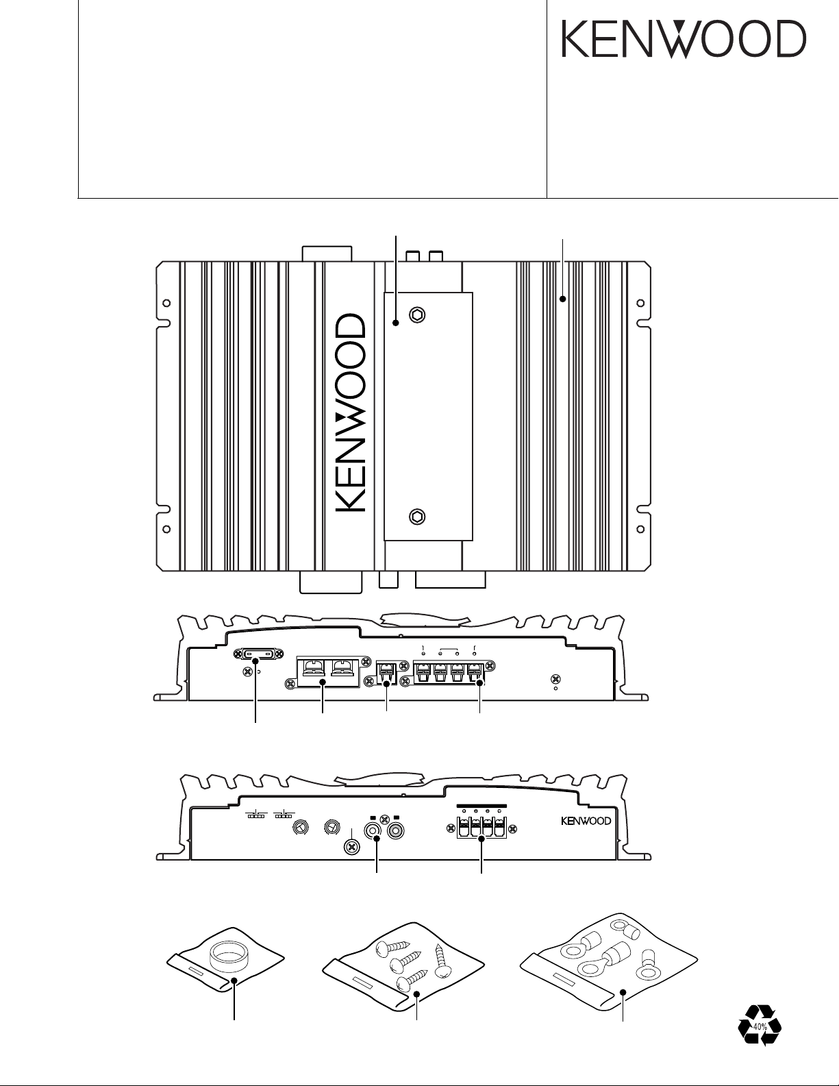
Dressing panel
(A21-4014-03)
SUBWOOFER AMPLIFIER
Heat sink
(F01-1627-01)
KAC-719
FUSE (30A)
30
Fuse
(F52-0015-05)
15Hz
25Hz
OFF
INFRASONIC
Accessory
(W01-1515-05)
POWER IN
BATT GND
Screw terminal
board
(E70-0820-05)
6dB
12dB
OFF
BASS
BOOST
FREQUENCY(Hz)
100
70
50 200
LPF
150
170
SENSITIVITY(V)
1
2
3
4
INPUT
0.5
5 0.2
P.CON(REMOTE)
Screw terminal
board
(E70-0818-05)
LINE IN
L
0.3
GND
Pin jack
(E63-0834-05)
Screw set
(N99-1587-05)
SERVO II
R
SPEAKER OUTPUT
Screw terminal
board
(E70-0808-05)
SPEAKER LEVEL INPUT
LEFT RIGHT
Screw terminal
board
(E70-0824-05)
SERVO II
SUBWOOFER
AMPLIFIER
Accessory (E type only)
(W01-0797-05)

KAC-719
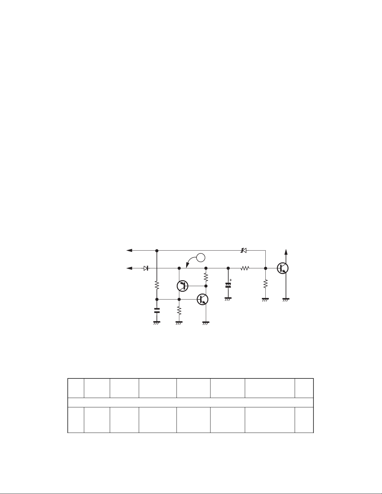
SP P-CON Switching Circuit
When the SP output from the head unit is connected to SP IN, the power can
be switched ON/OFF based on the DC voltage of the SP output. However, As
certain head unit models output DC permanently or generate a click during
switching OFF, it is required to provide the capability of previous P-CON
switching. A circuit which can perform the switching without using a switch
is described below.
This circuit performs switching by inhibiting the operation of the S-P-CON
circuit when a voltage is applied to the P-CON pin.
Circuit operation description
When the head unit is connected to SP-INN, the DC component in the SP output
turns Q38 ON through D32 and R158.
When a voltage is applied to the P-CON pin under this condition, Q45 is
turned ON via R188, positive feedback is applied by combination of Q45 and
Q46, Q45 and Q46 are held at ON, so the voltage at point (A) is almost 0 V
and the SP-P-CON circuit is not activated.
This circuit holds the ON status while the DC voltage from SP is present.
Therefore, in this condition, the P-CON circuit continues functioning. To
cancel the functioning, the voltage at the SP-IN pin should go 0 V.
CIRCUIT DESCRIPTION
to P-CON terminal
from SP-P-CON
D32
R188
100k
ADJUSTMENT
No ITEM
Connect a cassette receiver or other receiver.
IDLE
1
CURRENT
INPUT
SETTINGS
–
OUTPUT
SETTINGS
Connect a DC
voltmeter to CN3
A
Q46
Q45
TUNER
(RECEIVER)
SETTINGS
Volume : 0 VR3
ALIGNMENT
POINTS
D29
7.5v
R158
4.7k
10u 35
After sufficient aging
power control
ALIGN FOR FIG.
adjust to 2mV
Q38
3.3k
(a)
2

A B C D E F G IH
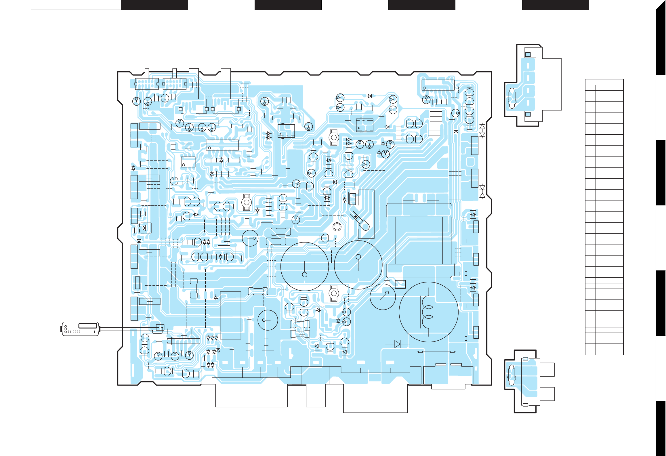
PC BOARD (Component Side View)
(a) 2mv
AUDIO UNIT
X09-5320-10 A/3 (J74-1030-11)
Q14
Q13
Q11
Q12
C22
E
B
D8
E
B
E
B
E
B
INFRASONIC
OFF/15Hz/25Hz
C20
W4
R91
R88
R102
W10
R92
W12
R86
W1
Q6
B
R76
E
R77
D7
R101
R90
W2
W3
TH1
W5
R85
W8
C74
BE
R168
W14
W9
W13
R84
C40
Q41
W16
W18
W15
R167
S1
C23
R42
R46
W23
W19
W11
W21
VR3
W17
W20
R89
R87
CN3
R166
R165
C73
Q28
C64
R110
BASS BOOST
OFF/6dB/12dB
S2
VR2
R49
R50
R32
C16
C17
R37
R38
W26
C25
W24
W22
W6
BE
R45
R51
R48
C24
85
IC2
1
R52
C21
R83
R82
BBEE
R104
Q16
C62
R106
W27
R103
W25
W29
W31
R81
W28
W30
W33
W7
R187
W34
R161
IC4
12345678
R164
R163
C72
Q27
W32
BE
R108
R31
4
R44
W36
Q10
C61
R80
C71
C63
W43
R47
W38
W37
C18
C19
R33
14
IC1
R41
W42
17
R9
C6
D10
R105
R19
R162
W39
R43
Q9
BE
Q15
BE
BE
Q8
W41
W40
C47
W44
D9
W45
W46
BE
Q7
D4
R78
C48
C38
W48 W47
W49
W50
W51
D11
D20
R27
B
E
R71
D12
D18
D3
Q4
W52
R75
D6
D19
D13
D15
D14
D17
D16
R107
R109
R10
W53
R73
R72
C12
B
E
W54
VR1
C14
8
R8
Q3
BE
Q5
C42
R96
W55
R36
C39
R74
C37
R25
R13
W56
C15
K1
R39
R30
R28
R79
W57
C36
R69
R17
C77
C78
R35
C13
R29
R93
C43
J5
W58
R40
R34
W59
W60
W61
R26
R11
W62
R224
W63
R225
D2
D1
W64
W65
C5
C3
D5
W66
R14
R70
R95
R66
W67
R65
R64
C33
W73
W68
W69
W70
W71
W72
R15
C1
W76
W74
W75
R12
C45
C44
R20
C46
1
J2
AUDIO UNIT
IC3
R142
R143
W101
C58
W102
9
W112
R144
R157
W103
W104
W105
W106
W107
W108
W109
W110
C59
D33
W113
W114
W115
Q30
W116
Q32
W117
W119
R135
R140
R141
W120
W121
R137
W122
BE
BE
EB
EB
W124
W125
Q29
Q31
G
D
S
G
D
S
D26
D25
D27
R139
Q33
E2
X09-C/3
16
18
C57
R112
R114
R116
Q18
BE
BE
Q17
C53
R113
R111
R115
R131
W99
W100
BE
BE
Q19
C54
W96
B
R160
Q40
Q24
R173
E
B
R23
R22
C65
R171
R170
C66
W97
D38
R21
C75
R24
CN2
W98
R228
D36
D35
L2
D40
C10
C68
C8
Q20
R118
R120
R117
R119
C67
R132
R7
R5
R6
R4
R3
R2
R1
CN1
C2
C4
C7
C9
W87
R229
D22
R18
R68
C35
R61
BE
BE
C11
R16
Q2
Q1
C31
W79
C34
C52
C32
R62
R63
R67
W80
Q23
R181
R183
C76
R186
W81
Q21
W82
R184
BE
R177
BE
Q26
D24
R176
R180
R194
W84
R185
R179
BE
BE
R182
BE
Q44
W88
R178
D37
Q22
D21
W86
W90
D23
R174
R172
R175
BE
E
Q25
W92
D34
D100
C51
Q35
R133
C55
W77
W78
R169
R193
C79
Q46
R227
R159
R226
EB
W83
Q45
BE
EB
R188
R155
R156
J4
Q39
D29
R151
D39
W85
Q38
R153
W93
W94
W91
C69
C70
D32
R158
W95
W89
BE
EB
Q37
R154
D30
R152
C56
D31
J3
TH2
L1
W201
W118
W202
CN4
R134
R136
W123
D28
R138
G
D
S
Q34
G
D
S
Q36
J1
E1
(X09-5320-10)
.oN.feR
CIQ
1C3
2B3
3F2
4B6
1D3
2D4
3C4
4C4
5C4
6B4
7C4
8C4
9C3
01C3
11B4
21B5
31B3
41B2
51C4
61B4
71F2
81F2
91F2
02F2
12D3
22E3
32D3
42E3
52E3
62E3
72B6
82B6
92G2
03G2
13G2
23G2
33G4
43G5
53G4
63G6
73E6
83E6
93D5
04E3
14B6
44E4
54D5
64D5
sserddA
2
3
4
5
6
Refer to the schematic diagram for the values of resistors and capacitors.
3
X09-B/3
7
4
 Loading...