

DVD/VCD/CD PLAYER
70%
76
0
POWER
ON OFF
4¢
1¡
DVF-3060/3060-S
DVF-3060K-S
SERVICE MANUAL
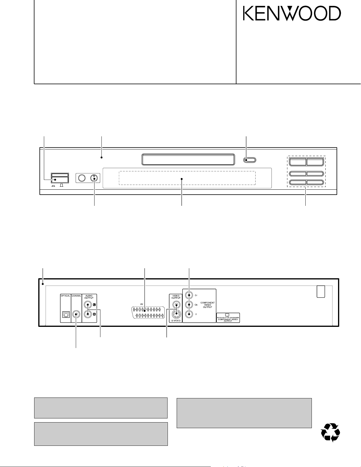
Knob(POWER) *
(K29-)
Front panel *
(A60-)
Knob(LEVEL)
(K29-8225-08)
Window display *
(B10-)
© 2002-4 PRINTED IN KOREA
B51-5789-00 (K/K) 2007
OPEN/CLOSE *
(K29-)
Knob *
(K29-)
Top cover *
(A09-)
Connection phono socket
(E63-1286-08)
Connection phono socket
(E63-1244-08)
In compliance with Federal Regulations, following are reproduction of labels on, or inside the product relating to laser
product safety.
Caution : No connection of ground line if disassemble
the unit. Please connect the ground line on
rear panel, PCBs, Chassis and some others.
Connection scart dual
(E40-8779-08)
Connection phono socket *
(E63-)
Connection din socket
(E63-1243-08)
KENWOOD-Corp. certifies this equipment conforms to DHHS
Regulations No.21 CFR 1040. 10, Chapter 1, subchapter J.
DANGER : Laser radiation when open and interlock defeated.
AVOID DIRECT EXPOSURE TO BEAM.
* Refer to parts list on page 16.
Figure is DVF-3060K.
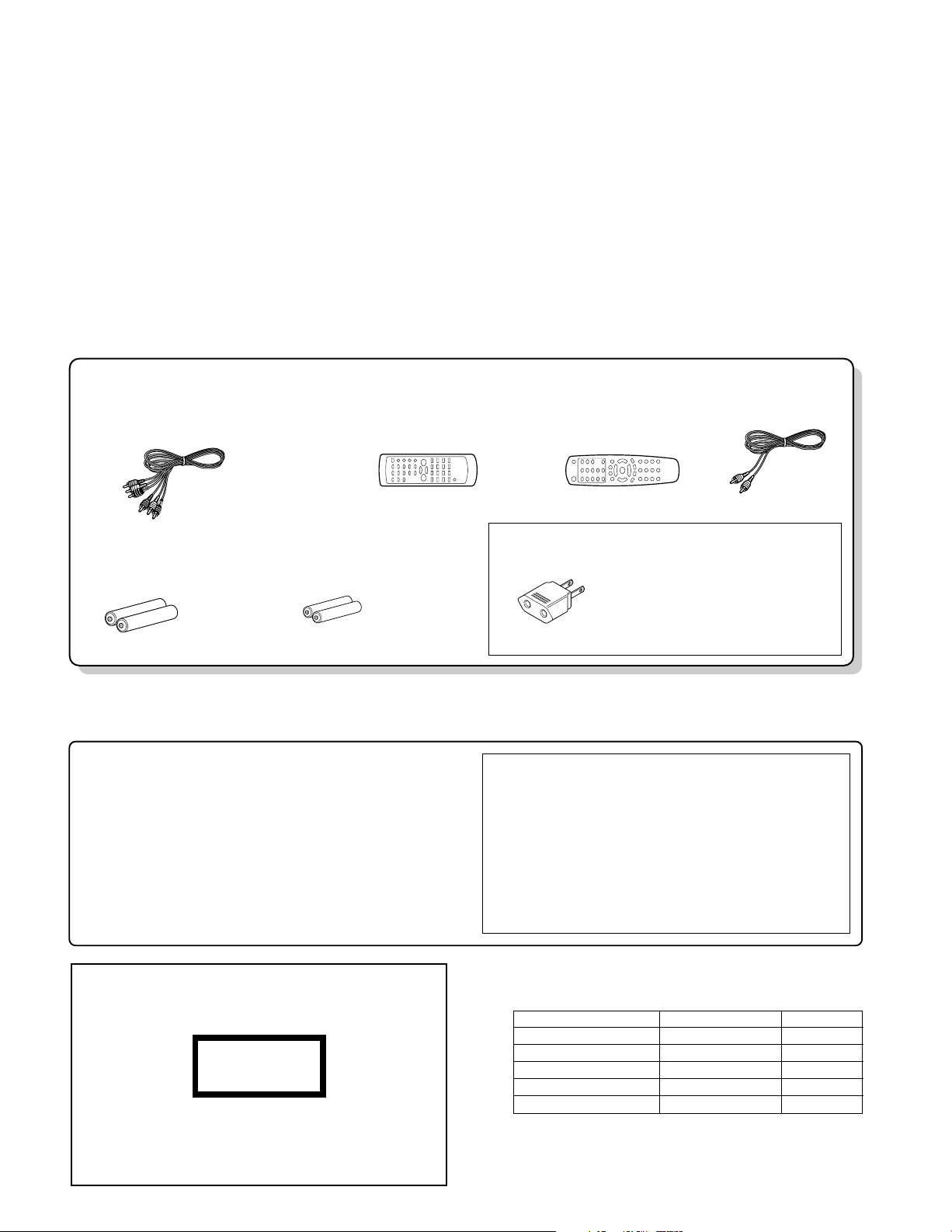
Please confirm that the following accessories are present.
Audio video cord (Red, White, Yellow) ...(1)
(E30-2990-08)
Batteries ...............................(2)
Remote control unit .........(1)
Coaxial cable ...(1)
(E30-7235-08)
DV-603/DVF-3060 (R6/AA)
DVF-3060K
(R03/AAA)
DVF-3060K
(A70-1592-08)
AC Plug Adaptor (1)
(E03-0115-05)
Use to adapt the plug on the
power cord to the shape of the
wall outlet.
(Accessory only for regions where
use is necessary.)
DV-603/DVF-3060
(A70-1532-08)
Operation to reset
÷ Please note that resetting the microprocessor clears the
contents stored in, it returns the microprocessor to the condition when it left the factory.
1 In Power ON condition, keep the 7 (Stop) key and the ¡
(Search) key pressed at the same time.
2 When both keys are pressed, the region code of the
unit, the software version, etc. will be displayed on
the display. (When nothing is done, the display of this
information continues.)
Example: 72. 14.02:05
3 Press the POWER ON/OFF switch to go to Power OFF.
4 When Power ON is performed with the
POWER ON/OFF
switch, the settings become the default factory settings.
The microprocessor may fall into malfunction (impossibility to operate erroneous display, etc.) when the
power cord is unplugged while power is ON or due to
an external factor. In this case, execute the following
procedure to reset the microprocessor and return it to
normal condition.
The marking of products using lasers
(For countries other than U.S.A., U.S.-Military and Canada)
The marking this product has been classified as Class 1. It
means that there is no danger of hazardous radiation outside
the product.
Location: Back panel
CLASS 1
LASER PRODUCT
DVF-3060/3060-S/3060K-S
CONTENTS / ACCESSORIES / CAUTIONS
Contents
CONTENTS / ACCESSORIES / CAUTIONS............. 2
DISASSEMBLY FOR REPAIR....................................3
CIRCUIT DESCRIPTION ............................................4
PC BOARD ................................................................ 9
Accessories
SCHEMATIC DIAGRAM .......................................... 13
EXPLODED VIEW ....................................................19
PARTS LIST..............................................................20
SPECIFICATIONS ....................................................25
Cautions
2
Model vs description
MODEL DESTINATION COLOR
DVF-3060 E BLACK
DVF-3060 Y BLACK
DVF-3060-S ETXY SILVER
DVF-3060K-S HM SILVER
DVF-3060K-S(M2) M2 SILVER
DVF-3060/3060-S/3060K-S
DISASSEMBLY FOR REPAIR
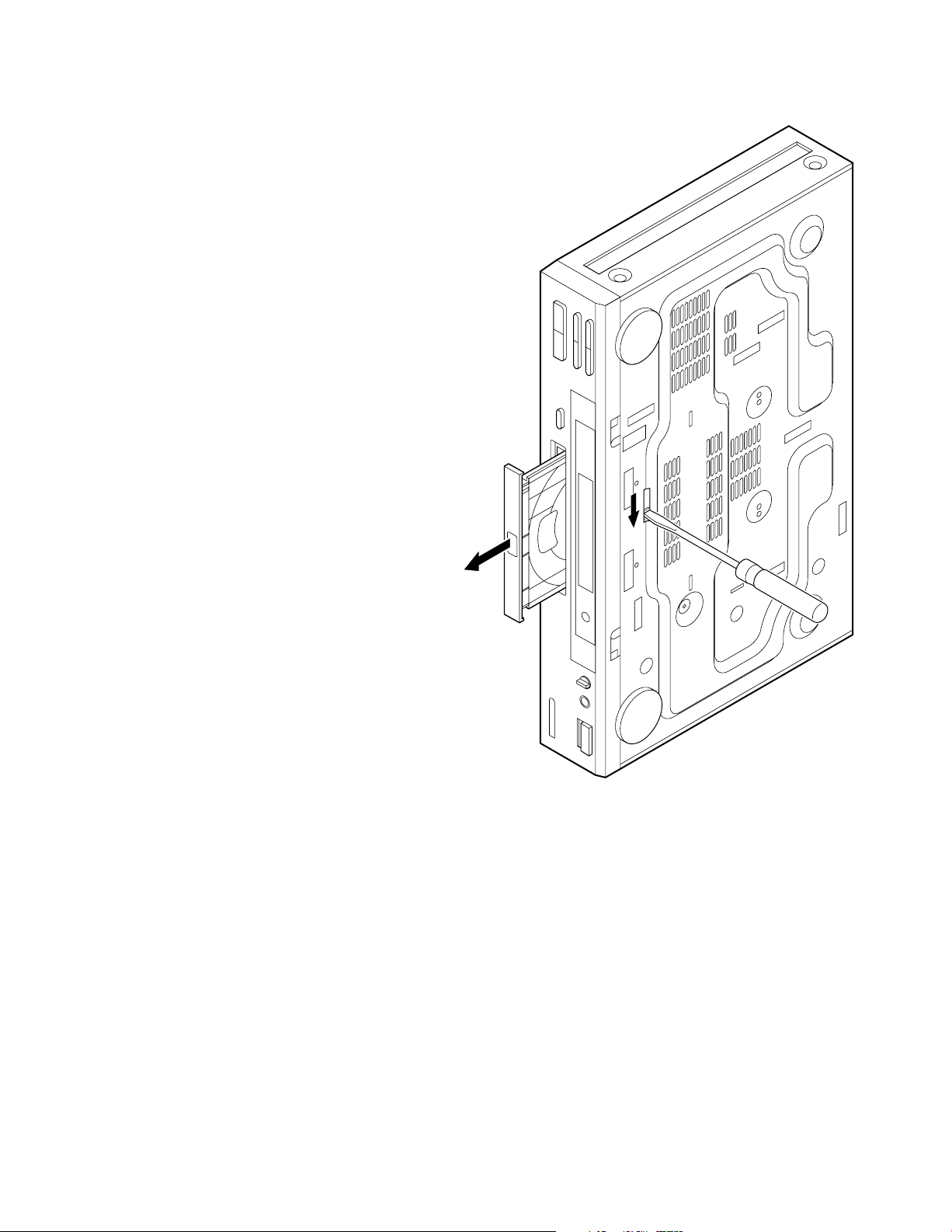
How to open the tray if it does not come out.
1. Insert a flat driver and pull it down in the drawing through the
hole on the loading chassis bottom.
2. Pull out the tray frontward by hand when it comes just out.
3
DVF-3060/3060-S/3060K-S
CIRCUIT DESCRIPTION
1. Port list sorted by function for MPEG Processor IC(Main IC21)
Port No. Port Name I/O Port Description
Audio DAC
51 DAC SCLK (BCK) O DAC sampling clock.
52 DAC PCMOUT0 O DAC PCM data out 0.
53 DAC PCMOUT1 O DAC PCM out 1 (unused).
54 DAC PCMOUT2 O DAC PCM out 2 (unused).
55 DAC PCMCLK O DAC PCM clock.
56 DAC LRCLK O DAC PCM Left/Right clock.
57 SPDIF OUT O Audio digital data output.
48 VDD PCM - Supply voltage for PCM (+2V5).
49 VSS PCM - Ground for PCM.
Clock & Reset
124 RESET I Chip reset input.
122 VDD PLL - Supply voltage for PLL (+2V5).
123 VSS PLL - Ground for PLL.
120 PIX CLK I 27MHz main clock input.
PIOs and communication
186 PIO0(0) T STROBE I/O Flash ROM down-load JIG module signal.
187 PIO0(1) MOD SW I/O Flash ROM down-load JIG module signal.
188 PIO0(2) VFD STB O VFD strobe output.
189 PIO0(3) VFD CLK O VFD clock output.
190 PIO0(4) VFD DATA OUT O VFD data output.
191 PIO0(5) VFD DATA IN I Data input from VFD.
192
193
194 PIO1(0) SDA I/O 12C serial data.
195 PIO1(1) SCL I/O 12C serial clock.
196
197 PIO1(3) TXD(JIG) I/O UART TXD
200 PIO1(4) RXD(JIG) I/O UART RXD
201 PIO1(5) FRONT TXDI I/O Unused.
202 TRIGGER IN I/O Trigger input from JIG.
203 TRIGGER OUT I/O Trigger output from JIG.
204 PIO2(0) H/P IND - Unused.
205 PIO2(1) FRONT RXD - Unused.
✽
✽
✽
✽
206 PIO2(2) MIC DET I Detection port of MIC jack.
207 PIO2(3) MIC MUTE - Unused.
208 PIO2(4) AUDIO MUTE O Audio mute control.
1 PIO2(5) RGB SEL(BLANK) I/O RGB sel (blank). E/T type only
2 PIO2(6) VIDEO MUTE I/O Video mute control.
3 PIO2(7) 16: 9 INDICATOR I/O 16 : 9 indicator (E/T type only)
6 PIO3(0) SCART H (TV/AUX) I/O Unused.
7 PIO3(1) I/O Unused.
8 PIO3(2) CSB O 3-wire MPU chip select/2-wire MPU interface address selection.
9 PIO3(3) SDIN O 3-wire MPU data output /2-wire MPU data output.
10 PIO3(4) IR REMOCON I/O IR Remote controller signal output.
11 PIO3(5) SCLK O 3-wire MPU clock output /2-wire MPU clock output.
12 PIO3(6) I/O Unused
13 PIO3(7) DVD RESET I/O Power- on reset of front-end module.
39 PIO4(0)HP MUTE - Unused.
40 PIO4(1) - Unused.
41 PIO4(2) DAC SCKDSD O DAC system clock output
PIO0(6) SLIDER SENSOR
OPEN/CLOSE (DRAWER POSITION)
PIO0(7) SLIDER IN
(DRAWER CCW/CTRL)
PIO1(2) SLIDER OUT
(DRAWER CW CTRL)
I/O Detection port of slider sensor for DVD mechanism.
I/O Control port of slider (IN) for DVD mechanism.
I/O Control port of slider (OUT) for DVD mechanism.
4
DVF-3060/3060-S/3060K-S
CIRCUIT DESCRIPTION
Port No. Port Name I/O Port Description
42 PIO4(3) DAC SDIDEM O DAC data output.
43 PIO4(4) DAC MUTEB O DAC mute control.
44 PIO4(5) DAC LAT12S O DAC latch output.
45 PIO4(6) DAC CSBIWL O DAC chip select.
46 PIO4(7) ZERO I/O Zero data flag.
Reserved
20 B WCLK I/O Unused.
21 B V4 I/O Unused.
22 NRSS OUT I/O Unused.
✽
✽
✽
✽
103 ADC SCLK I/O Digital audio port clock.
104 ADC LRCLK I/O ADC sample rate clock
105 ADC DATA I ADC digital audio data input.
106 ADC PCMCLK O Crystal input or master clock input (MCLK).
EMI Interface
161~170 CPU ADR(1~10) O Flash ROM address (1~10).
173~183 CPU ADR(11~21) O Flash ROM address (11~21).
141~148 CPU DATA(0~7) I/O Flash ROM data input/output (0~7).
151~158 CPU DATA(8~15) I/O Flash ROM data input/output (8~15).
138 CPU RAS1 I/O Unused.
131 CPU WAIT I Wait state (connected to be ground).
130 CPU RW O Unused.
128 CPU BE(0) O Flash ROM write enable.
129 CPU BE(1) O Unused.
139 CPU CAS0 O Unused.
140 CPU CAS1 O Unused.
135 CPU CE(0) O Unused.
134 CPU CE(1) O Unused.
133 CPU CE(2) O Flash ROM down-load JIG module select.
132 CPU CE(3) O Flash ROM chip select.
118 CPU PRO CLK O SDRAM clock (unused).
117 CPU OE I/O Flash ROM output enable.
Interrupt
127 IRQ(0) I Unused.
126 IRQ(1) I Unused.
125 IRQ(2) I Interrupt request 2 from front-end module.
Timers
116 PWM0 I/O Unused.
115 PWM1 I/O ROM boot option port (voltage low = emulator booting).
114 PWM2 I/O Unused.
JTAG
113 TCK I Test clock input from emulator module.
112 TDI I Test data input from emulator module.
111 TDO O Test data out to emulator module.
110 TMS I Test mode select.
109 TRST4 I Test reset from emulator module.
Front-end
16 B DATA I Pack data of front-end serial data.
17 B BCLK I Bit clock of front-end serial data.
18 B FLAG I Pack clock of front-end serial data.
19 B SYNC I Sector start of front-end serial data.
Video DAC
27,26,25 R/G/B (OUT) O R/G/B signal outputs.
32~34 Y/C/CV (OUT) O Y/C/CV signal outputs.
29 I REF RG I Reference current input for DAC RGB.
28 V REF RG I Reference voltage input for DAC RGB.
5
DVF-3060/3060-S/3060K-S
CIRCUIT DESCRIPTION
Port No. Port Name I/O Port Description
36 I REF YCC I Reference current input for DAC YCC.
35 V REF YCC I Reference voltage input for DAC YCC.
23 VDD RGB - Supply voltage for RGB (+2.5VA).
24 VSS RGB - GND
30 VDD YCC - Supply voltage for YCC (+2.5VA).
31 VSS YCC - GND
Shared memory interface
66~69 SMI ADR(3~0) O SDRAM address bus.
58~63 SMI ADR(4~9) O SDRAM address bus.
70~73 SMI ADR(10~13) O SDRAM address bus.
84~93 SMI DATA(0~9)
97~102 SMI DATA(10~15)
74 SMI CS(0) O Chip select bank 0.
75 SMI CS(1) - Unused.
76 SMI RAS O SDRAM RAS
77 SMI CAS O SDRAM CAS
78 SMI WE O SDRAM write enable
79 SMI DQML O DQ MASK enable low.
80 SMI DQMU O DQ MASK enable up.
82 SMI CLKIN I SDRAM clock input.
95 SMI CLKOUT O SDRAM clock out.
Power supply
4,47,81,107
136,159,184
14,37,64,94
119,149,171 VDD2 5 - 2.5V Power supply.
198
5,15,38,50,65
83,96,108,121
137,150,160
172,185,199
✽ M type only
VDD3 3 - 3.3V Power supply.
VSS - GND
I/O SDRAM data bus.
2. Description of Ics
2-1 VFO controller : uPD16311(IC91)
Pin No. Pin Name I/O Pin Description
6 DIN I Inputs serial data at rising edge of shift clock, starting from lower bit.
5 DOUT O
9 STB - Strobe pin.
8 CLK I Reads serial data at rising edge, and output data at falling edge.
52 OSC - Connect resistor for determining oscillation frequency to this pin.
15~26 S1/KS1~S12/KS12 O Segment output pins (Dual function as key source).
35~44 G10~G1 O Grid output pins.
27~30 S13~S16
31,32 12G,11G
46,47,49,50 LED (5,4,2,1) O Unused.
48 LED3 O Control pin of standby LED.
10~13 KEY1~KEY4 I Data input to these pins is latched at end of display cycle.
1~4 N.C. - Unused.
14,33,45 VDD - +5V power supply.
51 VSS - Connect this pin to GND of system.
34 VEE - -27V power supply.
7 N.C. - Unused.
6
Output serial data at falling edge of shift clock, starting from lower bit.
This is N-ch open-drain output pin.
O These pins are selectable for segment or grid output.
DVF-3060/3060-S/3060K-S
CIRCUIT DESCRIPTION
2-2 HEX Inverter (Single Stage) : M74HCU04(IC51)
Pin No. Pin Name I/O Pin Description
1,3,5,9,11,13 A0 to A5 I Data Inputs
2,4,6,8,10,12 Q0 to Q5 O Data Outputs
7 GND - Ground
14 VCC - Positive Supply Voltage
2-3 Flash Memory : M29W 800AT
Pin No. Pin Name I/O Pin Description
1~8 A15~A8 I Address Inputs
9,10 N.C. - Unused
11 WE - Write Enable
12 RP - Reset/Block Temporary Unprotect
13,14 N.C. - Unused
15 RY/BY O Ready/Busy/Output
16,17 A18,A17 I Address Inputs
18~25 A7~A0 I Address Inputs
26 CE - Chip Enable
27,46 VSS - Ground
28 QE - Output Enable
29~36
38~45
37 VCC - Supply Voltage
45 DQ15 I/O Data Input/Outputs or Address input
47 BYTE - Byte/Word Organization
48 A16 I Address Inputs
DQ0~DQ15 I/O Data Input/Outputs, Command Inputs
Truth Table
AQ
LH
HL
2-4 DC Motor Driver : KA8082(IC23)
Pin No. Pin Name I/O Pin Description
1 GND - Ground
2 VO1 O Output 1
3 VCTL I Motor speed control
4 VIN1 I Input 1
5 VIN2 I Input 2
6 SVCC - Supply voltage (Signal)
7 PVCC - Supply voltage (Power)
8 VO2 O Output 2
2-5 64 Bit SDRAM : HY57V641620HGT
Pin No. Pin Name I/O Pin Description
1,14,27, VCC - Power supply for internal circuits and input buffers.
2,4,5,7,8,10
11,13,42,44 45, DQ0~DQ15 I/O Multiplexed data input/output pin.
47,48,5051,53
3,9,43,49 VCCQ - Power supply for output buffers.
6,12,46,52 VSSQ - Ground for output buffer.
15,39 LDQM,UDQM I/O Controls output buffers in read mode and masks input data in write mode.
16,17,18 WE,CAS,RAS - WE, CAS and RAS define the operation.
19 CS - Enables or disables all inputs except CLK, CKE, and DQM.
20,21 BA0,BA1 -
22,23~26 A10, A0~A3
29~34,35 A4~A9, A11
28,41,54 VSS - Ground for internal circuits and input buffers.
36,40 NC - Unused.
37 CKE -
38 CLK I
Selects bank to be activated during RAS activity.
Selects bank to be read/written during CAS activity.
- Address bus : A0~A11
Controls internal clock signal and when deactivated, the SDRAM will be
one of the states among power down, suspend or self refresh.
The system clock input. all other inputs are registered to the SDRAM on
the rising edge of CLK.
7

DVF-3060/3060-S/3060K-S
CIRCUIT DESCRIPTION
2-6 Stereo Audio ADC : VM8739 (Main KIC1) M Type only
Pin No. Pin Name I/O Pin Description
1 SDIN I 3-wire MPU data input/2-wire MPU data input.
2 SCLK I 3-wire MPU clock input/2-wire MPU clock input.
3 XTI/MCLK I Crystal input or master clock input (MCLK).
4 XTO O Crystal output.
5 DCVDD - Digital core VDD.
6 DGND - Digital GND.
7 DBVDD - Digital buffers VDD.
8 BCLK I/O Digital audio port clock.
9,10 DNC - Unused.
11 ADCDAT O ADC digital audio data output.
12 ADCLRC I/O ADC sample rate clock.
13 NC - Unused.
14 AVDD - Analog VDD.
15 AGND - Analog GND.
16 VMID O Mid-rail reference decoupling point.
17 RLINEIN I Right channel line input (AC coupled).
18 LLINEIN I Left channel line input (AC coupled).
19 MODE I Control interface selection, pull up (on power up only).
20 CSB I 3-wire MPU chip select/2-wire MPU interface address selection.
2-7 24-bit, 192kHz Stereo DAC : WM8728 (Rear/Scart Board IC81)
Pin No. Pin Name I/O Pin Description
1 LRCIN I
2 DIN I Serial audio data input : PCM input mode Left channel DSD bitstream input : DSD input mode
3 BCKIN I Audio data bit clock input.
4 MCLK I Master clock input.
5 ZERO O Infinite zero detect flag.
6 DGND - Digital ground supply.
7 DVDD - Digital positive supply.
8 VOUTR O Right channel DAC output.
9 AGND - Analog ground supply.
10 AVDD - Analog positive supply.
11 VOUTL O Left channel DAC output.
12 VMID O Mid rail decoupling point.
13 VREFN - DAC negative reference.
14 VREFP - DAC positive reference.
15 CSBIWL I
16 MODE I Control mode selection.
17 MUTEB - Mute control. "L" = Mute on, "H" = Mute off"
18 SDIDEM -
19 SCKDSD I
20 LAT12S I
DAC sample rate clock input : PCM input mode
Right channel DSD bitstream input : DSD input mode
Software mode : 3-wire serial control chip select
Hardware mode : Input word length
Software mode : 3 or 2-wire serial control data input
Hardware mode : De-Emphasis select
Software mode : 3 or 2-wire serial control clock input
Hardware mode : DSD bitstream operation select
Software mode : 3-wire serial control load input
Hardware mode : Input data format selection
8

ACEBD
L501
KL04
L211
R222
R291
R292
R212
R401
R403
R512
R288
R238
R239
R240
R237
R241
R245
R244
R243
R511
R336
R307
R308
R325
J203
R266
C225
C228
C230
C229
C254
C311
C23S
C20S
J517
J518
R230
R298
C234
R276
J516
C252
KC07
KC08
KC06
KC04
KC01
KC11
C505
C406
C221
X501
C253
J515
C215
R290
R289
R242
R211
R210
R215
R213
R217
R233
R231
R232
R234
J211
R221
R223
R207
R265
R264
R287
R262
R286
R263
R407
R410
R409
R408
R256
C218
R236
J202
J201
R251
KC13
KR09
R333
R303
EBCEBCEBCEBCEBCEBC
R304
R305
R306
KR04
KR03
KR02
KR01
R273
R269
R270
R274
C226
C227
R293
R277
R278
R402
BE
Q201
BE
Q202
BE
Q203
CN25
Q22S
C23C
C20C
Q22C
C23Y
C20Y
Q22Y
C23R
1
1
1
19 1
1
58
41
1
7
1
1
1
15
14
2
1
1
1
52
156
105
53 104
208 157
24
4825
15
14
2
7
148
127
5428
1
2
10
20
11
4
85
218
5
19
18
2
29
28
2
C20R
Q22R
C23G
C20G
Q22G
C23B
C20B
C233
C232
RA48 RA47 RA46 RA45
RA35 RA37
RA36RA34
RA33
RA32RA31
RA44RA43RA42RA41
C204
C206
C210
Q22B
GND1A
CP21
CP26
CP24
CP25
D203
D202
D201
D204
CP28
GND1B
CP27
CP23
CP22
IC23
IC22
KIC1
IC51
IC41
IC21
IC31
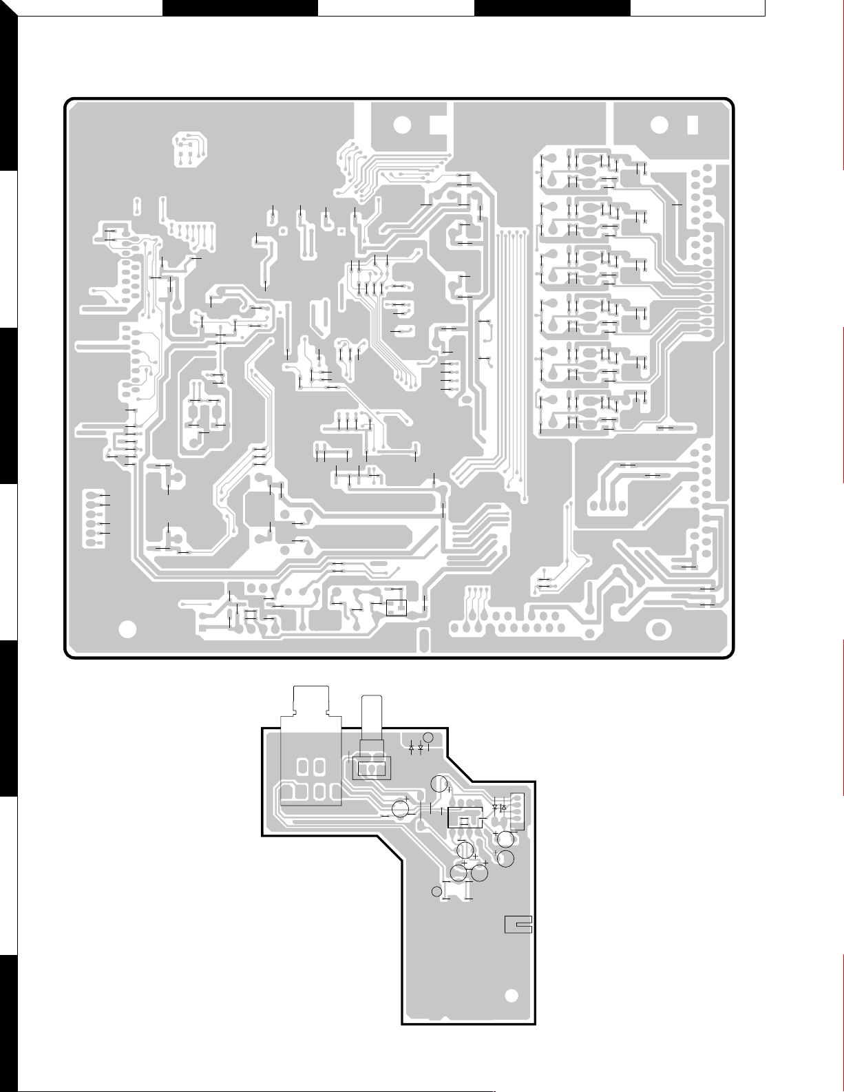
MAIN BOARD (SIDE A)
1
2
3
4
5
6
PC BOARD (Component side view
)
7
Refer to the schematic diagram for the value of resistors and capacitors.
9
F GIHJ
R415
L209
L20B
L20G
L201
L202
L203
L208
R406
R405
C404
R253
R254
C502C503
R503
C216
R246
R247
C217
R248
R250
R249
J212
C236
C237
C239
C240
KR05
KR06
KR07
KR08
KC10
KC09
R329
R328
R327
R323
R330
R502
C504
C501
R501
C219
R205
R209
C207
C208
C201
R208
C202
C203
C205
R216
R214
C209
C213
C211
C212
C214
R404
R413
C409
C223
C401
C402
C403
C224
C244
C235
C243
C242
R20B
R24B
R25B
C21B
C25B
J213
R24G
R25G
C21G
C25G
L20R
R24R
R25R
C21R
C25R
L20Y
R24Y
R25Y
C21Y
C25Y
L20C
R24C
R25C
C21C
C25C
L20S
L20
KL06
L206
L205
L204
KL05
KL01
KL02
L301
L207
KL03
R24S
R25S
C21S
C25S
R268
R326
R332
R331
R324
R338
R337
R315
R309
C314
C13
R267
R22B
R26B
C22G
R26G
C22R
R26R
C22Y
R26Y
C22C
R26C
C22S
R26S
R22B
R21B
R19B
R23B
C24B
R20G
R22G
R21G
R19G
R23G
C24G
R20R
R22R
R21R
R19R
R23R
C24R
R20Y
R22Y
R21Y
R19Y
R23Y
C24Y
R20C
R22C
R21C
R19C
R20SR19S
C308
R310
R311
R312
R313
C301
R302
R301
C302
R339
J301
C307
C306
C304
C305
KC12KC02
KC05
R322R321
C251
KC03
C310
R314
C309
C312
R23C
C24C
R22S
R21S
R23S
C24S
R204
R203
R202
R201
C220
R255
C222
R252
C305
Q204
MAIN BOARD (SIDE B)
EB
MC09
MR08
MR07
1
15
4
85
MR01
MR05
MC06
MR06
MR03
MJ04
MR02
MC10
MR04
MR09
MR11
MR10
MC04
MJ02
MJ03
MC02
MC05
MC08
MC07
MC03
MC01
MJK1
MVR1
MIC
LEVEL
LUG1
LUG2
MIC BOARD
MD03
MD04
MD02
MD01
MIC1
MCN1
MCP1
MJ01
PC BOARD (Component side view
1
2
3
)
4
5
6
7
10
Refer to the schematic diagram for the value of resistors and capacitors.

KMOQSLNPRT
J860
J861
J862
R845 R843
C836
J853
J852
J851
J850
J849
J866
J818
C825
J816
J811
J815
J814
J813
J812
J806
J807
J893
J869
J805
J804
J803
J802
C816
C814
C819
C802
C805
10 1
G
VCC
O
58
41
5
8
4
1
58
OGI
4
1
1
12
119 1 29
282
218
11 20
C809
C807
J810
C834
C832
C811
J848
C831
C713
C714
J888
J859
J858
J857
J856
J855
J854
J874
J847
J846
J834
J876
J829
J828
J857
J824
J823
J822
J821
J820
J819
J868
J889
J809
CN81
IC85
JK84
JK83
JK82
JK81
IC84
D805
CP82
CP81
COMPONENT
VIDEO
OUTPUT
VIDEO
OUTPUT
AUDIO
OUTPUT
COAXIAL
OPTICAL
REAR/SCART BOARD
R853
R854
C841
C842
R869
R870
L803
L802
C702
R714
R715
L704
R717
R720
R719
R722
R721
C704
R724
C715
C719
R723
R716
C722
R701
L705
R836
R868
C804
R804
L812
R841
R842
R835
C815
R833
R828
C812
R834
R891
R809
R825
R823
R824
R810
R704
R811
R813
R812
R814
R1
R2
R827
R718
C873
R878
R883
C872
L804
R871
R844
R847
R830
R850
R851
R862
R861
R872
R874
R875
R877
C840
R857
R856
R858
R855
R859
C839
R860
R848
R849
R852
EB
EB EB
EB
EB
EB
EB
EB
R829
R873
C717
C716
C718
L703
R731
R705
R734
R730
L706
R702
L707
R708
R709
R710
C703
R736
R821
R737
R822
R888
R837
R838
C817
R820
C833
R865 R831
R808
L801
C803
R806
R801
R802
R805
R803
C801
J801
C808
R816
R890
R840
R864
C829
R818
L813
R839
R863
R815
C813
C806
C828
C822
C823
C824
C826
C821
R817
C810
R819
R826
R866
R867
R832
E
B
EB
EB
EB
EB
EB
EB
EB
EB
EB
EB
EB
R876
R707
R706
C701
EB
20
21
2
1
D816
D817
D818
D707
D710
D819
D814
D815
D812
D813
D821
D822
D708
D709
D703
D801
D706
D705
D810
D811
Q810
Q809
Q813
Q815
Q817
Q705
Q814
Q812
Q816
Q806 Q807
Q808
Q701
JK71
Q702
Q704
Q805
Q804 Q803
Q811
Q802
Q801
IC86
IC83
IC82
IC81
D806
D702
D804
D701
R916
J901
J902
C903
R913
R912
R915
J903
J904
J905
38kHz JRC
J906
J907
R914
2
IG+B
11 5
J908
J909
J910
J911
J912
J914
J927
J917
J918
J920
J921
J922
J923
J924
J919
J913
J915
STOP
SEARCH-
SKIP-
PLAY/PAUSE
SEARCH+
J007
J925
SKIP+
J916
71
OPEN/CLOSE
R904
R903
R902
R901
R909
C904
C905
C902
C901
R910
R911
12 5 16 35 50 5354
1
13
14
2627
39
40
52
D905
CN91
RM91
LG92
SR01
SCP1
SLD1
SW91
CN92
SW93
SW94
SW96
SW92
SW95
SW97
D904
D902
D901
LG91
FL91
MCN1
SCN1
IC91
FRONT BOARD
PC BOARD(Component side view
1
2
3
)
4
5
6
7
Refer to the schematic diagram for the value of resistors and capacitors.
11 12

A BDFHJCEG I
CP21
CP27
CP22
D204
D202D203
D201
Q204
Q203
MECHA
F/E BOARD
CP28
CP2
CC201
PCM DATA
OUT(DAC)
MPEG IC
JIG
LOAD
DOWN
MIC
OPTION
FLASH
MEMORY
EEP ROM
ADC
DATA O UT
156
155
154
153
152
151
150
149
148
147
146
145
144
143
142
141
140
139
138
137
136
135
134
133
132
131
130
129
128
127
126
125
124
123
122
121
120
119
118
117
116
115
114
113
112
111
110
109
108
107
106
105
104
103
102
101
100
99
98
97
96
95
94
93
92
91
90
89
88
87
86
85
84
83
82
81
80
79
78
77
76
75
74
73
72
71
70
69
68
67
66
65
64
63
62
61
60
59
58
57
56
55
54
53
1
2
3
4
5
678
9
10
11
12
13
14
15
1617181920
21
22
232425
2627282930
31
32
333435
36
37
383940
41
42
43
44
45
4647484950
51
52
157
158
159
160
161
162
163
164
165
166
167
168
169
170
171
172
173
174
175
176
177
178
179
180
181
182
183
184
185
186
187
188
189
190
191
192
193
194
195
196
197
198
199
200
201
202
203
204
205
206
207
208
CPU DATA(13)
CPU DATA(12)
CPU DATA(11)
CPU DATA(10)
CPU DATA(9)
CPU DATA(8)
VSS
VDD2 5
CPU DATA(7)
CPU DATA(6)
CPU DATA(5)
CPU DATA(4)
CPU DATA(3)
CPU DATA(2)
CPU DATA(1)
CPU DATA(0)
CPU CAS1
CPU CAS0
CPU RAS1
VSS
VDD3 3
CPU CE(0)
CPU CE(1)
CPU CE(2)
CPU CE(3)
CPU WAIT
CPU RW
CPU BE(1)
CPU BE(0)
IRQ(0)
IRQ(1)
IRQ(2)
RESET
VSS PLL
VDD PLL
VSS
PIX CLK
VDD2 5
CPU PROCLK
CPU OE
PWM0
PWM1
PWM2
TCK
TDI
TDO
TMS
TRST
VSS
VDD3 3
ADC PCMCLK
ADC DATA
ADC LRCLK
ADC SCLK
SMI DATA(15)
SMI DATA(14)
SMI DATA(13)
SMI DATA(12)
SMI DATA(11)
SMI DATA(10)
VSS
SMI CLKOUT
VDD2 5
SMI DATA(9)
SMI DATA(8)
SMI DATA(7)
SMI DATA(6)
SMI DATA(5)
SMI DATA(4)
SMI DATA(3)
SMI DATA(2)
SMI DATA(1)
SMI DATA(0)
VSS
SMI CLKIN
VDD3 3
SMI DQMU
SMI DQML
SMI WE
SMI CAS
SMI RAS
SMI CS(1)
SMI CS(0)
SMI ADR(13)
SMI ADR(12)
SMI ADR(11)
SMI ADR(10)
SMI ADR(0)
SMI ADR(1)
SMI ADR(2)
SMI ADR(3)
VSS
VDD2 5
SMI ADR(9)
SMI ADR(8)
SMI ADR(7)
SMI ADR(6)
SMI ADR(5)
SMI ADR(4)
SPDIF OUT
(LRCIN)
(MCLK)
DAC PCMOUT2
DAC PCMOUT1
P102(5) RGB SEL(BLANK)
P102(6) VIDEO MUTE
P102(7) 16 : 9 INDICATOR
VDD3 3
VSS
P103(0) SCART H(TV/AUX)
P103(1)
P103(2)
P103(3)
P103(4) IR(REMOCON)
P103(5)
P103(6)
P103(7) DVD RESET
VDD2 5
VSS
B DATA
B BCLK
B FLAG
B SYNC
B WCLK
B V4
NRSS OUT
VDD RGB
VSS RGB
B OUT
G OUT
R OUT
V REF RG
I REF RG
VDD YCC
VSS YCC
Y OUT
C OUT
CV OUT
V REF YC
I REF YC
VDD2 5
VSS
P104(0) H/P MUTE
P104(1)
P104(2) DAC SCKDSD
P104(3) DAC SDIDEM
P104(4) DAC MUTEB
P104(5) DAC LATI2S
P104(6) DAC CSBIWL
P104(7) DAC ZERO
VDD3 3
VDD PCM
VSS PCM
VSS
DAC SCLK(BCK)
DAC PCMOUTO(DATA)
CPU DATA(14)
CPU DATA(15)
VDD3 3
VSS
CPU ADR(1)
CPU ADR(2)
CPU ADR(3)
CPU ADR(4)
CPU ADR(5)
CPU ADR(6)
CPU ADR(7)
CPU ADR(8)
CPU ADR(9)
CPU ADR(10)
VDD2 5
VSS
CPU ADR(11)
CPU ADR(12)
CPU ADR(13)
CPU ADR(14)
CPU ADR(15)
CPU ADR(16)
CPU ADR(17)
CPU ADR(18)
CPU ADR(19)
CPU ADR(20)
CPU ADR(21)
VDD3 3
VSS
PIO0(0) T STROBE
PIO0(1) MOD SW
PIO0(2) VFD STB
PIO0(3) VFD CLK
PIO0(4) VFD DATA OUT
PIO0(5) VFD DATA IN
PIO0(6) SLIDER SENSOR OPEN/CLOSE(DRAWER POSITION PI1)
PIO0(7) SLIDER IN(DRAWER CCW CTRL)
PIO1(0) SDA
PIO1(1) SCL
PIO1(2) SLIDER OUT(DRAWER CW CTRL)
PIO1(3) TXD(JIG)
VDD2 5
VSS
PIO1(4) RXD(JIG)
PIO1(5) FRONT TXDI
TRIGGER IN
TRIGGER OUT
PIO2(0) H/P IND
PIO2(1) FRONT RXD
PIO2(2) MIC DET
PIO2(3) MIC MUTE
PIO2(4) AUDIO MUTE
1
2
3
4
5
6
7
8
9
10
11
12
13
14
15
16
17
18
19
20
21
22
23
24
A15
A14
A13
A12
A11
A10
A9
A8
NC
NC
WE
RP
NC
NC
RY/BY
A18
A17
A7
A6
A5
A4
A3
A2
A1
48
47
46
45
44
43
42
41
40
39
38
37
36
35
34
33
32
31
30
29
28
27
26
25
A16
BYTE
VSS
DQ15
DQ7
DQ14
DQ6
DQ13
DQ5
DQ12
DQ4
VCC
DQ11
DQ3
DQ10
DQ2
DQ9
DQ1
DQ8
DQ0
OE
VSS
CE
A0
1
2
3
4
E0
E1
E2
VSS
8
7
6
5
VDD
WC
SCL
SDA
RA45 47
161
162
164
163
167
168
166
165
RA46 47
178
176
177
175
173
174
RA48 47
170
169
RA47 47
R407 47
R408 47
R410 47
R409 47
179
180
182
181
R263 47
R262 47
188
189
191
190
196
193
192
R289 47
R290 47
197
200
186
187
R264 75
R265 75
202
203
157
158
RA44 47
155
156
151
154
152
153
RA43 47
142
145
148
146
147
RA42 47
143
144
RA41 47
141
148
147
145
146
143
144
141
142
R401 47
R402 47
R256 47
R403 47
100u10
+
C221
0.01
C220
10
R254
0.1
C219
47
0.1
C222
10K
R255
R288 10K
10K
113
112
111
110
109
0.1
C218
115
0.1
C223
10K
47
133
128
3
1
6
2
R221 100
0.1
C201
8
10
R203 100
R204 100
R201 100
R202 100
161918
17
13
C202
0.1
100u10
+
C204
0.01
C203
2.2uH
L201
R205
100u10
C206
+
0.01
C205
L202
2.2uH
R19G 270
R19R 270
R19B 270 R19Y 270
R19C 270
R19S 270
R209
18K
R20Y 10
R20C 10
R20S 10
C207
0.1
R212 47
R213 47
R217 47
0.01
C209
100u10
+
C210
L203
2.2uH
C208
0.1
47
R232
10P
C211
47
R231
10P
C212
R210 47
34
33
32
44
45
46
42
25
26
27
51
52
+3.3V
+2.5V
R253R252
R404
R251
117
128
132
R223 47
1
2
3
4
5
6
7
8
9
10
11
12
13
14
15
16
17
18
19
D GND
SECTOR START
DATA VA LID
DATA(EXT DATA)
BIT CLOCK(EXT BCLK)
D GND
RESET(3V3 RESET)
DXX INTERRUPT(IRQ2)
SCL
SDA
D GND
DRIVE GND
+3V3D
+5VD
D GND
A GND
DISC M POWER
TRACK MAPOWER
1
2
3
4
5
6
7
IR REMOCON
+5.6VS
VFD STB
VFD DATA IN
VFD DATA OUT
VFD CLK
D GND
15
14
13
12
11
10
9
8
7
6
5
4
3
2
1
158
148
147
157
155
145
146
156
152
141
142
151
153
143
144
154
117
161
132
162
163
165
164
166
167
168
180
181
182
175
169
170
173
174
177
176
178 179
R411
0
128
47K
R413
R415
1.8K
R270
1.8K
R269
0.1
C225
47
R268
47
R267
10
R266
72
4
3
5
618
0
R337
0
R338
0
R336
22
R329
5.6K
R331
22
R330
+
C253
10u16
1.8K
R332
+
C254
100u16
22uH
L207
10K
R326
10K
R328
+
C252
1u50
5.6K
R323
68K
R325
10K
R324
10K
R327
470
R322
470
R321
0.1
C251
192
193
196
47K
R333
17
16
18
19
R273 100
R274 100
68P
C226
0.1
C234
68P
C227
13
R293 47
R276 0
R278 220
R277 220
R287 220
R286 220
189
190
191
188
+5.6V
10K
R406
10K
R405
186
141
142
148
145
143
144
147
146
117
133
128
187
0.1
C401
C402
0.1
0.1
C403
0.1
C224
+5V
+9V
470P
C216
117
12
12
+3.3V
+5V
+9V
+3.3V
+5V
+9V
+9V
+5V
+9V
+3.3V
+2.5V
+3.3V
+5V
+2.5V
+3.3V
+5V
+3.3V
+2.5V
+2.5V
+2.5V
+3.3V+3.3V
+2.5V
+5V
+9V
+3.3V
+2.5V
+3.3V
+2.5V
+3.3V
+5V
R412
0
C405
1000P
C404
1000P
+
C228
47u16
+
C229
47u16
+
C230
47u16
L204
L205
L206
+
100u10
C232
2.2uH
L209
470u6.3
C233
+
R20R 10
R20B 10
R20G 10
19
14
16
18
17
15
13
12
11
10
9
8
7
6
3
5
4
2
1
19
14
16
18
17
15
13
12
11
10
9
8
7
6
3
5
4
2
1
NC
2
1
21
R214 4.7K
L208
+5.6V
+5V
+3.3V
100u10
+
C406
R207
206
R208
10K
R298
0
R230
C242 10P
C243 10P
C235 10P
C244 10P
10
C239 100P
C237 100P
C236 100P
C238 100P
C241 33P
C240 100P
9
11
18K
DAC LRCLK
DAC PCMCLK
R211 4741R215 47
43
R216 4.7K
106
105
103
104
270
47
208
+2.5V
0
3.3V
0V
0V
3.3V
3.3V
3.3V
2.5V
3.3V
3.3V
2.4V
1.5V
1.6V
2.5V
2.5V
1.4V
0V
3.3V
3.2V
3.3V
3.3V
2.5V
2.5V
3.3V
4.7V
3.3V
1.2V
1.4V
0V
1.3V
1.3V
0V
1.5V
0.8V
3.3V
0V
3.3V
3.3V
5.3V
3.3V
3.3V
9.0V
9.0V
0V
0V
9.0V
0V
0.9V
0V
4.6V
5.3V
0V
4.7V
5.0V
5.0V
3.3V
5.2V
3.3V
3.3V
1.5V
5.3V
1.4V
3.3V
3.3V
3.3V
3.3V
9.0V
3.3V
3.3V
3.3V
5.3V
9.0V
4.7V
2.4V
0.9V
1.0V
0.9V
2.4V
0.8V
0.6V
0.8V
2.4V
3.3V
IC21
IC41
IC22
IC23
MAIN BOARD
1
2
3
4
5
6
7

TKMOQSLNPR
CP23
CP24
CP25
Q201
Q202
Q22R
Q22G
Q22B
IC23 : KA8082
IC21 :
IC22 : M24C02WMN6
IC31 : HY57V641620HGT
IC41 : M29W800AT
IC51 : M74HCU04MIR
Q204 : KTA1504S
Q22R,22G,22B,22S,
: KTN2907
D201 : UZ5V6
D202 : RB501V-40
D203,204 : IN4148
Q201-203 KTC3875S:
CP81
CP82
D706
D705
D707
D708
D710
D709
D703
Q702
Q704
D702
D701
IC82 (2/2)
IC82 (1/2)
Q803
Q811
D804
Q802
Q801
CN81
Q814
Q816
Q812
Q817
Q705
Cb
Y
JK84
Cr
Q815Q809Q813
JK83-A
JK83-B
EXCEPT
(E,T)TYPE
(E,T)TYPE
(E,T)TYPE
ONLY
CONNECTION
JTAG TEST
Q701
2
1
VIDEO
OUTPUT
COMPONENT
VIDEO
HEX UNBUFFERED
INVERTER
SDRAM
R OUT
G OUT
B OUT
CVBS
C
Y
V MUTE
SPDIF
OUT
EXCEPT
CC802
CC801
S-VIDEO
D806
+6V
AVR
DAC
Cb
Cr
Y
AUDIO
(Lch)
L. P. F.
OUTPUT
(Lch)
AUDIO
MCN1
MIC1 (1/2)
MIC1 (2/2)
MIC
LEVEL
MIC
AMPLIFIER
MIC
MJK1
MD3
MD4
MD1
MD2
Q22Y
Q22C
Q22S
CN25
SPDIF
OUT
CP26
MIC OPTION
DV-603/DVF-3060
OPTION
MIC
OPTION
ONKYO
SCART
OPTION
KIC1 : WM8739EDS
22C,22Y
MD1-4 1N4148:
STEREO
AUDIO
DAC
CV OUT
C OUT
Y OUT
:MIC1 BA4558-1
1
2
3
4
5
6
7
8
9
10
11
12
13
14
15
16
17
18
19
20
21
22
23
24
25
26
27
VCC
DQ0
VCC Q
DQ1
DQ2
VSS Q
DQ3
DQ4
VCC Q
DQ5
DQ6
VSS Q
DQ7
VCC
LDQM
WE
CAS
RAS
CS
BA0
BA1
A10
A0
A1
A2
A3
VCC
54
53
52
51
50
49
48
47
46
45
44
43
42
41
40
39
38
37
36
35
34
33
32
31
30
29
28
VSS
DQ15
VSS Q
DQ14
DQ13
VCC Q
DQ12
DQ11
VSS Q
DQ10
DQ9
VCC Q
DQ8
VSS
NC
UDDM
CLK
CKE
NC
A11
A9
A8
A7
A6
A5
A4
VSS
1
2
3
4
5
6
7
AO
QO
A1
Q1
A2
Q2
GND
14
13
12
11
10
9
8
VCC
A3
Q3
A4
Q4
A5
Q5
RA36 47
RA37 47
RA34 47
RA35 47
0
J301
+3.3V
R309 100
R339
10
R308 100
R307 100
R306 100
R305 100
R303 100
R304 100
R302 100
R301 100
4.7K
R310
4.7K
R312
4.7K
R311
4.7K
R313
76
74
77
78
79
80
82
RA33 47
RA32 47
RA31 47
R234 47
R233 100
10P
C213
10P
C214
+2.5V
102
101
100
99
93
92
97
98
89
88
90
91
87
84
86
85
69
68
71
70
62
67
66
63
59
58
60
61
55
56
57
+2.5V
+3.3V
+2.5V
73
72
1
2
3
4
5
6
7
8
9
10
11
12
13
14
15
TRGI OUT
TRGI IN
GND(OPTION)
TMS
GND
TCK
GND
TDI
GND
TDO
+5VD
TXD(JIG)
RXD(JIG)
JTAG RST
TRST
1
2
3
4
5
6
7
8
9
10
11
12
13
14
15
16
17
18
19
M GND
+9VM
M GND
NC
+2.5VD
D GND
+5VD
D GND
+3.3VD
NC
A-MUTE
V-MUTE
+6VA
A GND
P/RESET
+12VA
A GND
-12VA
NC
1
2
3
4
5
6
7
8
9
10
11
12
13
14
15
16
17
18
19
20
21
22
23
24
25
26
27
28
29
CVBS
A GND
C(CROMA)
A GND
Y(LUMI)
A GND
R(PR)
A GND
G(Y:LUMI)
A GND
B(PB)
A GND
PCM LRC OUT
PCM DATA OUT
PCM BCK OUT
PCM MCLK OUT
DAC ZERO IN
DAC DGND
DAC AGND
DAC CSBIWL OUT
DAC MUTEB IN/OUT
DAC SDIDEM IN/OUT
DAC SCKDSD OUT
DAC LATI2S OUT
D GND
SPDIF
16 : 9
BLANK
TV/AUX
72
73
70
69
68
67
66
79
78
77
76
74
91
85
90
89
88
87
86
84
60
59
58
62
61
63
80
82
71
93
92
97
99
98
100
101
102
R315
47K
0.1
C312
+
C311
100u10
0
R314
+3.3V
+3.3V
+3.3V
L501
+
C505
470u6.3
0.1
C504
1M
R503
C503
X501
C502 56
R502
100
R501
20P
C501
1K
R2500R249
0.1
C217
4.7K
R246
4.7K
R247
10K
R248
0
J202
0
J201
0.1
C215
10K
R243
10K
R244
10K
R245
R236
47K
R240 47
47
R239
47
R238
R237 47
R241 47
10K
R242
109
200
197
111
112
113
110
115
202
203
0
R26R
390P
C24R
12
R24R
8.2
R25R
390P
C25R
2.7uH
L20R
3300P
C21R
+
C23R
220u16
0.1
C22R
2.2K
R22R
75
R23R
820
R21R
470u10
+
C20R
R26G
C24G
C21G
R25G
3300P
R22G
2.2K
R23G
75
R21G
820
C20G
470u10
12
R24G
C25G
390P
390P
2.7uH
L20G
220u16
C23G
C22G
8.2
0.1
+
0
3300P
R25B
C21B
C24B
470u10
2.2K
R22B
75
R23B
R21B
C20B
820
12
R24B
8.2
C25B
390P
390P
L20B
2.7uH
220u16
C22B
C23B
0.1
+
0
R26B
L210
7
9
11
25
26
27
+3.3V
+2.5V
+12V
2
208
3
1
57
42
44
41
43
45
9
46
55
11
7
5
1
3
A GND
G(Y)
A GND98
A GND
CVBS
R(PR)
Y(LUMI) 5
6
7
3
4
A GND12
C(CROMA)
PCM BCK IN
DAC DGND
DAC ZERO OUT
PCM LRC IN
A GND
PCM DATA IN
PCM MCLK IN
A GND
B(PB)
17
18
14
15
16
12
13
10
11
21
DAC MUTEB
DAC SDIDEM
D GND
SPDIF
DAC SCKDSD IN
DAC LATI2S IN 24
26
25
23
22
DAC CSBIWL IN 20
DAC AGND 19
NC
BLANK
16 : 9
29
28
27
+6VA 13
RESET
A GND1514
D GND 8
V-MUTE
A-MUTE1211
NC
+3.3VD109
+2.5VD 5
D GND
+5VD67
NC
M GND 3
4
+9.5VM
MG 1
2
100u10
C831
+
VREFP
DVDD
SCKDSD
BCKIN
5
6
7
DGND
ZERO
4
MCLK
16
CSBIWL
MODE
15
14
SDIDEM
MUTEB
18
17
LRCIN
2
3
DIN
1
19
LATI2S
20
8
VREFN
VOUTR
13
+2.5V
+3.3V
+5V
+9V
+9V
+3.3V
+2.5V
+9V
+3.3V
+2.5V
+2.5V
+3.3V
+3.3V
+3.3V+3.3V
+2.5V
+5V
+3.3V
1K
1K
0
R736
R733
0
10u50
+
C714
10u50
+
C713
680
R715
680
R714
120
10
R718R717
0
100P
C716
100P
C717
R719
010
R720
100P
C718
10P
C704
10P
C873
0
R721 R722
10
120
100u10
+
C719
1K
R723
100
R701
1K
R716
+
C703
100u16
100u16
+
C71539R731
R724
180
51
R730
L703
L706
L705
47
R734
100
R702
1K
R710
1K
L707
1K
R709
1K
R708
10P
C821
22
23
24
21
+
C809
10u50
560P
13
14
15
5
6
8
7
3
2
4
1
OUT
GND
IN
47u16
+
C832
330
R867
47u16
C834
+
47u16
C819
+
330
R827
47u16
C816
47u16
+
C811
3.9K
R864
5.6K
R840
47K
R835
2200P
C815
47u16
C814
330P
C829
9.1K
R818
2200P
C812
47K
R828
5.6K
R839
3.9K
R863
330P
C813
9.1K
R815
+
C836
220u16 0
R844
22 2W
R843
100
R826
100
R866
100P
C833
100K
R865
100P
C817
100K
R819
+
820K
R831
+
100
R806
180
R805
0.01
C803
10
R804
4.7K
R803
R824 0
R823 0
R811 0
R812 0
R817 0
R814 0
11
28
24
26
27
20
21
22
16
17
7
9
1
3
5
9+5VD
+8VM-
12
M GND
10NC
11
4+12VD
7D GND
8+2.5VD
6+3.5VD
5P/RESET
2A GN D
-12VA 3
12VA 1
+2.5V
+5V
+12V
+8V
+3.3V
+6V
5
1
3
26
1K
R883
120
R876
R873
120
120
R877
+
C701
220u10
0.1
C702
68
R707
470
R706
R829 0
10
8
9
7
60
R869
0
R870
0
R871
120
R875
120
R872
120
R874
7
9
11
1
31
24
+
+
+
+3.3V
+3.3V
+5V
+5V
+5V
+6V
+6V
+5V
+6V
+5V
+5V
+5V
+12V
2
0
R832
L804
L802
L803
0.1
C872
4.7K
R888
1K
R705
16
19
17
18
NC
A GND
-12VA
+12VA
+12V
22 2W
R845
32
33
31
30
IN/OUT
IN/OUT
R809 0
13
14
R810 0
R825 0
15
R813 0
23
7
9
11
9
AGND
10
AVDD
12
VMID
11
VOUTL
16
17
0
R890
560P
J873
47u16
+
C805
1K
C806
C807
560P
C808
10u50
+
L812
R704
0
C810
1000u6.3
C802
+
33
R841
0
R891
R842 33
47K
20
C828 10P
C822 10P
C823 10P
C824 10P
C826 10P
0
J801
11
9
7
28
+9VM
+12V
L704
L813
1K
27
+12V
12V
R816
AGND 1
MIC
-12V23
+12 4
MIC DET 5
MR5
220
220
MR4
10u50
MC2
+
10u50
MC3
+
1
3
4
2
8
7
6
5
0.1u50
+
MC1
MR1
100K
MR2
100K
1K
MR3
MR6 82K
MC6 470P
20K(B)
MVR1
4.7u50
MC4
+
0.47u50
+
MC5
0
MJ4
10u50
+
MC7
1K
MR7
MR8 100K
MR9 100K
MC9 680P
0.47u50
+
MC8
MR10 10K
2.2K
MR11
6
5
4
2
8
9
7
3
1
1000P
MC10
MIC1
0
J212
0
L301
33
R24Y
12
C20Y
R23Y
32
2.2K
R22Y
75
470u10
+
820
R21Y
2.2K
R22C
R23C
75
+
R25Y
220u16
C24Y
C25Y
390P
390P
2.7uH
L20Y
8.2
5
R26Y
0
C22Y
3300P
C21Y
+
C23Y
0.1
C25C
C24C
390P
390P
L20C
2.7uH
3
R24C
12
R24S
12
R21C
820
470u10
C20C
75
R23S
2.2K
R22S
34
820
R21S
C20S
++
470u10
L20S
R26C
0
3300P
220u16
C23C
C22C
8.2
R25C
0.1
+
C21C
390P
390P
C24S
C25S
2.7uH
1
0
0.1
C23S
C22S
220u16
R25S
8.2
3300P
C21S
+
R26S
+6V
+6V
+6V
51
52
56
L211
DGND
SPDIF1
2
0
J208
1098
7
65432
1
DNC
DNC
BCLK
DBVDD
DGND
DCVDD
XTO
XTI/MCLK
SCLK
SDIN
11
12
131415
16
17
181920
ADCDAT
ADCLRCNCAVDD
AGND
VMID
RLINEIN
LLINEIN
MODE
CSB
KR7 47
KR8 47
KR1 47
KR2 47
KR3 47
KR4 47
9
11
106
KR5 10K
2.2uH
KL1
0.1
KC2
10u16
+
KC1
KL2
2.2uH
10u16
KC11
0.1
KC12
+
103
104
105
KL3
2.2uH
10u16
KC4
0.1
KC3
+
0.1
10u16
+
KC6
KC5
10u16
KC8
+
KC7
10u16
+
47P
KC9 47P
KC10
8
KR6 47
+3.3V
+12VA4
-12VA
AGND
K MIC12
3
MIC DET5206
DESTINATION
COUNTRY
C502,
24P
ABB.
503
22P
U.S.A. K
Y
PX
JAPAN
J
EEUROPE
TU.K.
GENERAL MARKET
M
AUSTRALIA
X
6
R291 47
R222 47
R292 47
0.1
C722
+5V
CANADA P
KOREA H
IC21
STI5519
STI5508
22P
24P
12V
+12V
12V
+12V
+12V
+12V
12V
+12V
12V
+12V
12V
+12V
12V
+5V
12V
12V
+12V
3.3V
0V
1.4V
1.4V
0V
0V
0V
0V
1.4V
1.5V
3.3V
3.3V
2.5V
3.3V
4.4V
5.0V
2.9V
4.4V
5.0V
2.9V
5.0V
2.9V
4.4V
5.9V
9.0V
2.5V
3.3V
3.3V
12.2V
-12.6V
3.3V
9.0V
5.3V
2.5V
12.2V
9.0V
2.5V
9.2V
5.9V
5.3V
5.9V
4.1V
-11.4V
10.9V
12.2V 11.7V
-12.6V
-12.1V
2.9V
5.0V
2.9V
4.4V
4.4V
5.0V
2.9V
5.0V
4.4V
5.3V
0V
0.7V
3.3V
IC31
IC51
IC81
IC85
REAR/SCART B'D
MAIN BOARD MIC BOARD : (M,H)TYPE ONLY
KIC1
C314
10P
C313
10P
D822 D821
D817 D816
D812 D813
D814 D815
D810 D811
D822 D821
JK71
Lch
Rch
JK82
D805
Q804
Q805
JK81
Q802
Q814
KTA1504S:
KTC3875S:
KIA7806
GP1F32T
BA4560F
WM8728
IC85
IC84
:
:
IC82
IC81
:
:
Q804 KRA107S:
Q809,812,813,815-817
KTD1304:
Q803,811 DTC323T:
D703,705-710,810-819,821,822
Q701,705,801
D701,702,804,806
Q702,704,805
KTC3875S
DTC114YKA
1SS355
ZNR5V1B0.2W
:
:
:
:
CN91
CN92
D905
D902
D901
D904
SW94
SW93
SW91
SW95
SW92
SW96
SW97
STOP
SKIP
FORWARD
SKIP
BACKWARD
SEARCH
FORWARD
SEARCH
BACKWARD
OPEN/
CLOSEPAUSE
PLAY
CN1
D1-D4
D5
ZD1
PC1
D6
CN2
CN3
D7
D8
ZD2
D9
D10
D12
D15
U3
D17
D13
1
2
D805, J873 1N4148:
ZD2 : 1N5226B
D13
D10,12
D15
ZD1
D7
: SR204
1N5239B:
1N5819
SF24
HER105
:
:
:
:U2 KA7809
D1-4,17
D6,8,9
D5
U4
1N4007
1N4937
HER107
:
:
:
KIA7042AP
:
U1 KA1M0380R-YDTU:
1N4004
1N4148
:D905
D901,902,904 :UPD16311-QFP40IC91
W02-2801-08
:
:RM91
OUTPUT
AUDIO
KA431AZU3
:
OPTICAL
COAXIAL
ONLY
(E,T)TYPE
MUTE
A MUTE
SW1
SCN1
FL DRIVER
REMOTE
SENSOR
AR OUT
AL OUT
BLUE
GREEN
C/RED
Y/CVBS OUT
SENSE
BLK
CVBS IN
21
19
13
15
17
7
9
11
1
3
5
20
18
16
14
6
10
12
8
4
2
0
R836
+
C825
330u6.3
0
R868
470
R838
R837
1
2
3
5
4
0
0
R808
100P
C804
100
R801
1000P
C801
OUT
VCC
GND
2
1
3
1
2
0
R820
1
2
3
4
5
GND
+5VFL DC
-27VFL DC
-5VFL DC
+5V6S
1
2
3
4
5
6
7
IR REMOCON
VFD STB
VFD DATA OUT
VFD DATA IN
VFD CLK
GND
52515049484746454443424140
39
38
37
36
35
34
33
32
31
30
29
28
27
14
15
1617181920
21
22
232425
26
1
2
3
4
5
6
7
8
9
10
11
12
13
OSC
VSS
LED1
LED2
LED3
LED4
LED5
VDD
G1
G2
G3G4G5
G6
G7
G8
G9
G10
VEE(-27V)
VDD
G11
G12
S16
S15
S14
S13
VDD
S1/KS1
S2/KS2
S3/KS3
S4/KS4
S5/KS5
S6/KS6
S7/KS7
S8/KS8
S9/KS9
S10/KS10
S11/KS11
S12/KS12
DOUT
DIN
CLK
STB
KEY1
KEY2
KEY3
KEY4
R914 15
10
0.047
C902
R916
10u16
C903
+
100
R911
+B
GND
IN
4.7K
R910
10K
R904
10K
R901
10K
R902
10K
R903
10K
R909
10K
R905
R906
10K
10K
R907
R908
10K
KEY1
KEY4
KEY3
KEY2
KEY4
KEY3
KEY2
KEY1
+5.6V
+5.6V
+5.6V
+5.6V
+5.6V
+5.6V
+5.6V
+5.6V
27V 27V
27V
1
2
F1
VR1
0.1
C1
TH1
LF1
C4 C3
C2 0.1
C7 2200P
R1 150K 2W
R2 56K 1W
C6 47u400
+
34
DRAIN
VCC
21
FB
GND
0.047
C8
1K
R3
47u50
C9
+
R4 68K
T1
1
2
3
4
5
GND
FL5V+
-27V
FL5V-
5.5VS
1
2
3
4
5
6
7
8
9
10
11
12
+12VA
AGND
-12VA
+12VD
P/REST
+3.5V
DGND
+2.5V
+5V
NC
MGND
+9VM
100u16
C10
+
1K
R7
3
R6
12K
R10
1u50
C11
+
20
R9
120
R8
2.2
R11
1K
R12
100u25
C12
+
6
4
1
2
8
7
9
14
12
13
10
15
11
1000P
C1310R13
100u25
C15
+
560 1W
R14
220u25
C14
+
15uH
L1
VIVO
GND
3.3
R15
100u16
C16
+
100 1W
470u10
R17
C19
+
15uH
470u10
C18
+
L2
1.2K
GND
C21
10u50
VO+VI
R18
51K
R19
C20
?
+
12K
R20
470u10
C24
1000u10
+
C23
L3
7uH
+
120
R22
1u50
+
C25
10
R25
18K
R23
1.5K
R26
2.2K
R24
820
R28
150
R27
R29
390
2200P
C27
220
R30
100u16
C26
+
27V
+9V
+9V
+5.5V
+5.5V
+5.5V
+3.5V
+2.5V
+12V
+5V
+12V
2200P2200P
1/2W
+B
R802
0
+5V
1K
L801
10
R16
1000P
C17
1/2W
1/2W
1/2W
R21
10
C22
1000P
C5
2200P
R5
5.6
2200P
C28
0.1
C904
50
49
48
47
46
45
44
43
42
41
40
39
38
37
36
35
34
33
32
31
30
29
28
27
26
25
24
23
22
21
20
19
18
17
16
15
14
13
12
11
10
9
8
7
6
5
4
3
2
1
P1
P2
P3
P4
P5
P6
P7
P8
P9
P10
P11
P12
P13
P14
P15
P16
NX
12G
11G
10G
9G
8G
7G
6G
5G
4G
3G
2G
1G
NP
NP
F1
F1
NX
NX
NX
NX
NX
NX
NX
NX
NX
NX
NX
NX
NX
NX
NX
NX
NX
F2
54
F2
NP
NP
51
53
52
R915 15
FL-
R913 15
R912 15
0.1
C905
FL+
+5V6S
+5.6V
IC
1000P
C901
S3
S1
S2
S4S8S7
S6
S5
S12
S11
S10
S9
S13
S14
S15
S16
G12
G11
S1
S2
S4
S3
S6
S7
S8
S5
S12
S11
S9
S10
S14
S15
S13
S16
G11
G12
G10
G9
G8
G7
G6
G5
G4
G2
G3
G1
G10
G9
G8
G6
G7
G4
G3
G2
G5
G1
FL+
FL-
2
1 +5.6V
3
1
2
AC250V 2A
12V
12V
-28.1V
5.0V
5.7V
5.2V
-28.1V
5.7V
-12.6V
12.2V
11.93V
5.3V
5.7V
1.05V
9.0V
2.5V
3.3V
4.7V
IC84
REAR/SCART B'D
IC91
RM91
U1
U2
U4
POWER SUPPLY BOARD Replace with new one only if defective.
FRONT BOARD
FL91
DV-603/DVF-3060
(2G-11G)
(1G)
S2S1 S3 S4
a
b
g
m
c
e
p
n
r
d
k
j
h
f
12G 7G 6G8G 5G 1G10G
DP COL
9G 4G 3G 2G11G
DP COL
P1
8G9G11G 10G12G 7G
P2
P3
P5
a
P4
P8 m
g
n
P9
P7
k
b
j
P6
h
P15
P14
P15
P12
P13
P11
e
d
r
c
p
P10
f
a
m
g
n
k
b
j
h
e
d
r
c
p
f
6G 5G 4G 3G 2G 1G
DP
a
m
g
n
k
b
j
h
e
d
r
c
p
f
DP
a
m
g
n
k
b
j
h
e
d
r
c
p
f
COL
a
m
g
n
k
b
j
h
e
d
r
c
p
f
COL
a
m
g
n
k
b
j
h
e
d
r
c
p
f
a
m
g
n
k
b
j
h
e
d
r
c
p
f
a
m
g
n
k
b
j
h
e
d
r
c
p
f
a
m
g
n
k
b
j
h
S1
S4
S3
S2
e
d
r
c
p
f
a
m
g
n
k
b
j
h
e
d
r
c
p
f
B LINE
B LINE
GND LINE
SIGNAL LINE
DIGITAL LINE
B
+B
U VXZABADWYAAAC
CAUTION: For continued safety, replace safety critical components only with manufacturer's recommended parts (refer
to parts list). indicates safety critical components. For
continued protection against risk of fire, replace only with
same type and rating fuse(s). To reduce the risk of electric
shock, leakage-current or resistance measurements shall be
carried out (exposed parts are acceptably insulated from the
supply circuit) before the appliance is returned to the customer.
The DC voltage is an actual reading measured with a high
impedance type voltmeter with no signal input. The measurement value may vary depending on the measuring
instruments used or on the product.
DVF-3060/3060-S/3060K-S
Y22-8672-00

3x10 (BLK)
3x8 (SIL)
3x18
3x8
3x6
: N89-3010-45
: N89-3008-41
: N09-5269-08
: N89-3008-46
: N89-3006-46
A
B
C
D
E
SW91
SW94 SW95
SW96 SW97
SW93
FL91
SW92
COAXIAL
IC84JK81JK82
OPTICAL
OUTPUT
AUDIO
JK71
AV
JK83JK84
S-VIDEO
COMPONENT
VIDEO OUTPUT
OUTPUT
VIDEO
MJK1 MVR1
MIC LEVEL
ON OFF
POWER
SW1
DVF-3060
A
A
A
D
D
E
x2
Dx2
Dx2
Dx2
D
C
C
C
D
D
D
D
D
A
A
A
A
A
705
752
633
624
615
602
619
601
620
604
621
644
632
632
632
611
624
623
623
645
625
622
625
Dx2
706
626x2
631x2
609
637
639
603
610
640
608
638
627
x2
D
D
D
D
A or B
A or B
A
x2 or Bx2
Ax2 or Bx2
Ax3 or Bx3
D
D
D
D
D
D
D
753
751
707
746
Parts with exploded numbers larger than 700 are not supplied.
A
B
C
19
1
2
EXPLODED VIEW (UNIT)
DVF-3060/3060-S/3060K-S

20
✽ New Parts
Parts without Parts No. are not supplied.
Les articles non mentionnes dans le Parts No. ne sont pas fournis.
Teile ohne Parts No. werden nicht geliefert.
New
Ref. No
Add-
ress
Parts
Parts No.
Description
DV-603/DVF-3060/DVF-3060-S/DVF-3060K-S
601 1A ✽ A09-1269-08 COVER TOP -BK 55266340 KPEY B
601 1A ✽ A09-1270-08 COVER TOP -S 55269550 ETXY S
601 1A ✽ A09-1270-08 COVER TOP -S 55269550 HMM2 S
602 1B ✽ A29-1206-08 DOOR TRAY -BK 55262410 KPEY B
602 1B ✽ A29-1207-08 DOOR TRAY -S 55269400 ETXY S
602 1B ✽ A29-1207-08 DOOR TRAY -S 55269400 HMM2 S
603 2A ✽ A60-2272-08 PANEL FRONT -BK 55269770 EY B
603 2A ✽ A60-2273-08 PANEL FRONT -S 55269350 ETXY S
603 2A ✽ A60-2275-08 PANEL FRONT K-S 55269360 HMM2 S
603 2A ✽ A60-2276-08 PANEL FRONT 603 55262390 KP
604 1A A70-1532-08 REMOTE CONTROL55235390 KPETXY
604 1A ✽ A70-1592-08 REMOTE CONTROL55330330 HMM2
608 2A ✽ B10-3872-08 WINDOW DISPLAY 55330230 EY B
608 2A ✽ B10-3873-08 WINDOW DISPLAY- 55346790 ETXY S
608 2A ✽ B10-3873-08 WINDOW DISPLAY- 55346790 HMM2 S
608 2A ✽ B10-3874-08 WINDOW DISPLAY 55266230 KP
609 2A ✽ B11-1560-08 WINDOW FILTER 55266220
610 2A B43-0302-04 KENWOOD BADGE 55220500
611 1B ✽ B43-0333-08 DVD-VIDEO BADGE 55266270
- B46-0096-53 CARD WARRANTY 55195100 X
- B46-0310-03 CARD WARRANTY 55213810 ET
- B46-0328-03 LIMITED WARRANT 55218520 Y
- B46-0336-03 CARD WARRANTY 55235440 P
- B46-0365-04 CARD QUESTION 55373590 KP
- B59-1104-00 CARD ADDRES(PX) 55219940 Y
- ✽ B60-5233-08 BOOK INST(EN) 55398740 KPETXY
- ✽ B60-5233-08 BOOK INST(EN) 55398740 MM2
- ✽ B60-5234-08 BOOK INST(FR) 55398840 PE
- ✽ B60-5235-08 BOOK INST(GE/NE 55399140 E
- ✽ B60-5236-08 BOOK INST(IT/ES 55399240 E
- ✽ B60-5237-08 BOOK INST(TC) 55398940 M
- ✽ B60-5238-08 BOOK INST(AR) 55399040 M2
615 1B ✽ D40-1799-08 OK KIT TVM503R 10757650
619 1A E03-0115-05 AC PLUG ADAPTOR55236070 MM2
620 1A E30-2990-08 AUDIO-CABLE ST 55176530
621 1A E30-7235-08 COAXIAL 55186190
622 1C E30-7250-08 AC CORD 55190780 KPY
622 1C E30-7251-08 AC CORD 55190790 EMM2
622 1C E30-7252-08 AC CORD 55190800 T
622 1C E30-7253-08 AC CORD 55190820 X
622 1C ✽ E30-7280-08 AC CORD 55330320 H
623 1B,2C ✽ E35-3382-08 FFC CABLE 19X70 55318540
624 1C ✽ E35-3383-08 FFC CABLE 19X50 55318530
625 1C,2C ✽ E35-3384-08 FFC CABLE 29X50 55318430
626 2C ✽ G11-2896-08 FOOT RUBBER R18 55266290
627 2B ✽ G11-2897-08 FOOT RUBBER F29 55266280
- ✽ H10-7865-08 CUSHION LEFT 55291910
- ✽ H10-7866-08 CUSHION RIGHT 55291930
- H21-1523-08 SHEET 820X820 55164920
- H25-1712-08 BAG 260X410 55170650
- H25-1739-08 BAG POLY AC COR 55259730
Desti-
nation
1
Re-
marks
✽ New Parts
Parts without Parts No. are not supplied.
Les articles non mentionnes dans le Parts No. ne sont pas fournis.
Teile ohne Parts No. werden nicht geliefert.
New
Ref. No
- ✽ H50-4527-08 GIFT BOX K/P 55291940 KP
- ✽ H50-4528-08 GIFT BOX Y 55294730 Y B
- ✽ H50-4529-08 GIFT BOX XS 55294710 X
- ✽ H50-4530-08 GIFT BOX E 55294610 E B
- ✽ H50-4532-08 GIFT BOX ES 55294620 E S
- ✽ H50-4533-08 GIFT BOX TS 55294640 T
- ✽ H50-4534-08 GIFT BOX K-S 55294650 M
- ✽ H50-4535-08 GIFT BOX K-S/M2 55294690 M2
- ✽ H50-4618-08 GIFT BOX YS 55346810 Y S
- ✽ H50-4630-08 GIFT BOX K-S 55374690 H
631 2B ✽ J02-1549-08 FOIL FOOT 55266310
632 2B J19-6169-08 BRKET SPACE PCB 55164980
633 1C J42-0350-08 CLAMP CORD 55125180
637 2A ✽ K29-8218-08 OPEN/CLOSE -BK 55266190 KPEY B
637 2A ✽ K29-8219-08 OPEN/CLOSE -S 55269420 ETXY S
637 2A ✽ K29-8219-08 OPEN/CLOSE -S 55269420 HMM2 S
638 2B ✽ K29-8221-08 PLAY KEY -BK 55266210 KPEY B
638 2B ✽ K29-8222-08 PLAY KEY -S 55269510 ETXY S
638 2B ✽ K29-8222-08 PLAY KEY -S 55269510 HMM2 S
639 2A ✽ K29-8225-08 KNOB LEVEL K-S 55304220 HMM2 S
640 2A ✽ K29-8226-08 KNOB POWER -S 55269480 ETXY S
640 2A ✽ K29-8226-08 KNOB POWER -S 55269480 HMM2 S
640 2A ✽ K29-8228-08 KNOB POWER -BK 55266200 KPEY B
C N09-5269-08 SCREW 3X18 55127290
644 1B ✽ W02-2947-08 SMPS MODULE 55274690 ETXY
644 1B ✽ W02-2947-08 SMPS MODULE 55274690 HMM2
644 1B ✽ W02-2948-08 SMPS MODULE KP 55329440 KP
645 2C ✽ W02-2951-08 MAIN PCB ASSY 55291270 KP
645 2C ✽ W02-2952-08 MAIN PCB ASSY 55305890 ETXY
645 2C ✽ W02-2953-08 MAIN PCB ASSY 55305940 HMM2
Add-
ress
Parts
Parts No.
Description
Desti-
nation
MAIN PCB
C20B CE04LW1A471M ELECTRO 470UF 10WV
C20C CE04LW1A471M ELECTRO 470UF 10WV
C20G CE04LW1A471M ELECTRO 470UF 10WV
C20R CE04LW1A471M ELECTRO 470UF 10WV
C20S CE04LW1A471M ELECTRO 470UF 10WV
C20Y CE04LW1A471M ELECTRO 470UF 10WV
C21B CK73GB1H332K CHIP C 3300PF K
C21C CK73GB1H332K CHIP C 3300PF K
C21G CK73GB1H332K CHIP C 3300PF K
C21R CK73GB1H332K CHIP C 3300PF K
C21S CK73GB1H332K CHIP C 3300PF K
C21Y CK73GB1H332K CHIP C 3300PF K
C22B CK73GB1C104Z CHIP C 0.10UF Z
C22C CK73GB1C104Z CHIP C 0.10UF Z
C22G CK73GB1C104Z CHIP C 0.10UF Z
C22R CK73GB1C104Z CHIP C 0.10UF Z
C22S CK73GB1C104Z CHIP C 0.10UF Z
C22Y CK73GB1C104Z CHIP C 0.10UF Z
C23B CE04LW1C221M ELECTRO 220UF 16WV
C23C CE04LW1C221M ELECTRO 220UF 16WV
C23G CE04LW1C221M ELECTRO 220UF 16WV
C23R CE04LW1C221M ELECTRO 220UF 16WV
2
Re-
marks
DVF-3060/3060-S/3060K-S
PARTS LIST
L : Scandinavia K : USA P : Canada R : Mexico C : China I : Malaysia
Y : PX(Far East,Hawaii) T : England E : Europe G : Germany V : China(Shanghai)
Y : AAFES(Europe) X : Australia Q : Russia H : Korea M : Other Areas indicates safety critical components .
B: BLACK S:SILVER
L : Scandinavia K : USA P : Canada R : Mexico C : China I : Malaysia
Y : PX(Far East,Hawaii) T : England E : Europe G : Germany V : China(Shanghai)
Y : AAFES(Europe) X : Australia Q : Russia H : Korea M : Other Areas indicates safety critical components .

✽ New Parts
Parts without Parts No. are not supplied.
Les articles non mentionnes dans le Parts No. ne sont pas fournis.
Teile ohne Parts No. werden nicht geliefert.
New
Ref. No
C23S CE04LW1C221M ELECTRO 220UF 16WV
C23Y CE04LW1C221M ELECTRO 220UF 16WV
C24B CC73GCH1H391J CHIP C 390PF J
C24C CC73GCH1H391J CHIP C 390PF J
C24G CC73GCH1H391J CHIP C 390PF J
C24R CC73GCH1H391J CHIP C 390PF J
C24S CC73GCH1H391J CHIP C 390PF J
C24Y CC73GCH1H391J CHIP C 390PF J
C25B CC73GCH1H391J CHIP C 390PF J
C25C CC73GCH1H391J CHIP C 390PF J
C25G CC73GCH1H391J CHIP C 390PF J
C25R CC73GCH1H391J CHIP C 390PF J
C25S CC73GCH1H391J CHIP C 390PF J
C25Y CC73GCH1H391J CHIP C 390PF J
C201,202 CK73GB1C104Z CHIP C 0.10UF Z
C203 CK73GB1H103K CHIP C 0.010UF K
C204 CE04LW1A101M ELECTRO 100UF 10WV
C205 CK73GB1H103K CHIP C 0.010UF K
C206 CE04LW1A101M ELECTRO 100UF 10WV
C207,208 CK73GB1C104Z CHIP C 0.10UF Z
C209 CK73GB1H103K CHIP C 0.010UF K
C210 CE04LW1A101M ELECTRO 100UF 10WV
C211-214 CC73GCH1H100D CHIP C 10PF D
C215 CK73GB1C104Z CHIP C 0.10UF Z
C216 CC73GCH1H471J CHIP C 470PF J
C217-219 CK73GB1C104Z CHIP C 0.10UF Z
C220 CK73GB1H103K CHIP C 0.010UF K
C221 CE04LW1A101M ELECTRO 100UF 10WV
C222-225 CK73GB1C104Z CHIP C 0.10UF Z
C226,227 CC73GCH1H680J CHIP C 68PF J
C228-230 CE04LW1C470M ELECTRO 47UF 16WV
C232 CE04LW1A101M ELECTRO 100UF 10WV
C233 CE04LW0J471M ELECTRO 470UF 6.3WV
C234 CK73GB1C104Z CHIP C 0.10UF Z
C235 CC73GCH1H100D CHIP C 10PF D
C236-241 CC73GCH1H101J CHIP C 100PF J
C242-244 CC73GCH1H100D CHIP C 10PF D
C251 CK73GB1C104Z CHIP C 0.10UF Z
C252 CE04LW1H010M ELECTRO 1.0UF 50WV
C254 CE04LW1C101M ELECTRO 100UF 16WV
C311 CE04LW1A101M ELECTRO 100UF 10WV
C312 CK73GB1C104Z CHIP C 0.10UF Z
C313,314 CC73GCH1H100D CHIP C 10PF D
C401-403 CK73GB1C104Z CHIP C 0.10UF Z
C404,405 CK73GB1H102K CHIP C 1000PF K
C406 CE04LW1A101M ELECTRO 100UF 10WV
C501 CC73GCH1H200J CHIP C 20PF J
C502,503 CC73GCH1H220J CHIP C 22PF J KPYH
C502,503 CC73GCH1H240J CHIP C 24PF J ETXMM2
C504 CK73GB1C104Z CHIP C 0.10UF Z
C505 CE04LW0J471M ELECTRO 470UF 6.3WV
KC01 CE04LW1C100M ELECTRO 10UF 16WV HMM2
KC02,03 CK73GB1C104Z CHIP C 0.10UF Z HMM2
KC04 CE04LW1C100M ELECTRO 10UF 16WV HMM2
KC05 CK73GB1C104Z CHIP C 0.10UF Z HMM2
Add-
ress
Parts
Parts No.
Description
Desti-
nation
3
Re-
marks
✽ New Parts
Parts without Parts No. are not supplied.
Les articles non mentionnes dans le Parts No. ne sont pas fournis.
Teile ohne Parts No. werden nicht geliefert.
New
Ref. No
KC06-08 CE04LW1C100M ELECTRO 10UF 16WV HMM2
KC09,10 CC73GCH1H470J CHIP C 47PF J HMM2
KC11 CE04LW1C100M ELECTRO 10UF 16WV HMM2
KC12 CK73GB1C104Z CHIP C 0.10UF Z HMM2
CP21 E40-8985-08 CONN 1.25MM 19 55124600
CP22,23 E35-3010-08 CONN 1.0MM 15 F 55125910
CP24 E40-8985-08 CONN 1.25MM 19 55124600
CP25 E40-8987-08 CONN 1.25MM 29 55138650
CP26 E40-8777-08 CONN 2.0MM 5 MA 55123320 HMM2
CP27 E40-8765-08 CONN 2.0MM 7 MA 55090060
CP28 E40-8771-08 CONN 2.5MM 02 M 55164790
KL01-03 L90-0363-08 LF-SMD 2U2H +10 55188040 HMM2
L20B ✽ L90-0400-08 LF-SMD 2U7H +10 55190450
L20C ✽ L90-0400-08 LF-SMD 2U7H +10 55190450
L20G ✽ L90-0400-08 LF-SMD 2U7H +10 55190450
L20R ✽ L90-0400-08 LF-SMD 2U7H +10 55190450
L20S ✽ L90-0400-08 LF-SMD 2U7H +10 55190450
L20Y ✽ L90-0400-08 LF-SMD 2U7H +10 55190450
L201-203 L90-0363-08 LF-SMD 2U2H +10 55188040
L204-206 L32-1047-08 FBEAD SURFACE M55126670
L207 L90-0361-08 LF-SMD 22U0H +1 55185100
L209 L90-0363-08 LF-SMD 2U2H +1055188040
L210 L32-1047-08 FBEAD SURFACE M55126670
L211 L32-1045-08 FBEAD SURFACE M55126710
L501 L32-1047-08 FBEAD SURFACE M55126670
R415 L32-1047-08 FBEAD SURFACE M55126670
X501 L77-2326-08 FILQZ 27M0 HZ + 55128980
C253 CE04LW1C100M CE 10U0F +20% 115002130
J201-203 RK73GB1J000J CHIP R 0 J 1/16W
J211,212 RK73GB1J000J CHIP R 0 J 1/16W
J301 RK73GB1J000J CHIP R 0 J 1/16W
KR01-04 RK73GB1J470J CHIP R 47 J 1/16W HMM2
KR05 RK73GB1J100J CHIP R 10 J 1/16W HMM2
KR06-08 RK73GB1J470J CHIP R 47 J 1/16W HMM2
L208 RK73GB1J000J CHIP R 0 J 1/16W
L301 RK73GB1J000J CHIP R 0 J 1/16W
R19B RK73GB1J271J CHIP R 270 J 1/16W
R19C RK73GB1J271J CHIP R 270 J 1/16W
R19G RK73GB1J271J CHIP R 270 J 1/16W
R19R RK73GB1J271J CHIP R 270 J 1/16W
R19S RK73GB1J271J CHIP R 270 J 1/16W
R19Y RK73GB1J271J CHIP R 270 J 1/16W
R20B RK73GB1J100J CHIP R 10 J 1/16W
R20C RK73GB1J100J CHIP R 10 J 1/16W
R20G RK73GB1J100J CHIP R 10 J 1/16W
R20R RK73GB1J100J CHIP R 10 J 1/16W
R20S RK73GB1J100J CHIP R 10 J 1/16W
R20Y RK73GB1J100J CHIP R 10 J 1/16W
R21B RK73GB1J821J CHIP R 820 J 1/16W
R21C RK73GB1J821J CHIP R 820 J 1/16W
R21G RK73GB1J821J CHIP R 820 J 1/16W
R21R RK73GB1J821J CHIP R 820 J 1/16W
R21S RK73GB1J821J CHIP R 820 J 1/16W
Add-
ress
Parts
Parts No.
Description
Desti-
nation
4
Re-
marks
PARTS LIST
DVF-3060/3060-S/3060K-S
L : Scandinavia K : USA P : Canada R : Mexico C : China I : Malaysia
Y : PX(Far East,Hawaii) T : England E : Europe G : Germany V : China(Shanghai)
Y : AAFES(Europe) X : Australia Q : Russia H : Korea M : Other Areas indicates safety critical components .
21
L : Scandinavia K : USA P : Canada R : Mexico C : China I : Malaysia
Y : PX(Far East,Hawaii) T : England E : Europe G : Germany V : China(Shanghai)
Y : AAFES(Europe) X : Australia Q : Russia H : Korea M : Other Areas indicates safety critical components .

22
DVF-3060/3060-S/3060K-S
✽ New Parts
Parts without Parts No. are not supplied.
Les articles non mentionnes dans le Parts No. ne sont pas fournis.
Teile ohne Parts No. werden nicht geliefert.
New
Ref. No
R21Y RK73GB1J821J CHIP R 820 J 1/16W
R22B RK73GB1J222J CHIP R 2.2K J 1/16W
R22C RK73GB1J222J CHIP R 2.2K J 1/16W
R22G RK73GB1J222J CHIP R 2.2K J 1/16W
R22R RK73GB1J222J CHIP R 2.2K J 1/16W
R22S RK73GB1J222J CHIP R 2.2K J 1/16W
R22Y RK73GB1J222J CHIP R 2.2K J 1/16W
R23B RK73GB1J750J CHIP R 75 J 1/16W
R23C RK73GB1J750J CHIP R 75 J 1/16W
R23G RK73GB1J750J CHIP R 75 J 1/16W
R23R RK73GB1J750J CHIP R 75 J 1/16W
R23S RK73GB1J750J CHIP R 75 J 1/16W
R23Y RK73GB1J750J CHIP R 75 J 1/16W
R24B RK73GB1J120J CHIP R 12 J 1/16W
R24C RK73GB1J120J CHIP R 12 J 1/16W
R24G RK73GB1J120J CHIP R 12 J 1/16W
R24R RK73GB1J120J CHIP R 12 J 1/16W
R24S RK73GB1J120J CHIP R 12 J 1/16W
R24Y RK73GB1J120J CHIP R 12 J 1/16W
R25B RK73GB1J8R2J CHIP R 8.2 J 1/16W
R25C RK73GB1J8R2J CHIP R 8.2 J 1/16W
R25G RK73GB1J8R2J CHIP R 8.2 J 1/16W
R25R RK73GB1J8R2J CHIP R 8.2 J 1/16W
R25S RK73GB1J8R2J CHIP R 8.2 J 1/16W
R25Y RK73GB1J8R2J CHIP R 8.2 J 1/16W
R26B RK73GB1J000J CHIP R 0 J 1/16W
R26C RK73GB1J000J CHIP R 0 J 1/16W
R26G RK73GB1J000J CHIP R 0 J 1/16W
R26R RK73GB1J000J CHIP R 0 J 1/16W
R26S RK73GB1J000J CHIP R 0 J 1/16W
R26Y RK73GB1J000J CHIP R 0 J 1/16W
R201-204 RK73GB1J101J CHIP R 100 J 1/16W
R205 RK73GB1J183J CHIP R 18K J 1/16W
R207 RK73GB1J470J CHIP R 47 J 1/16W HMM2
R208 RK73GB1J271J CHIP R 270 J 1/16W HMM2
R209 RK73GB1J183J CHIP R 18K J 1/16W
R210-213 RK73GB1J470J CHIP R 47 J 1/16W
R214 RK73GB1J472J CHIP R 4.7K J 1/16W
R215 RK73GB1J470J CHIP R 47 J 1/16W
R216 RK73GB1J472J CHIP R 4.7K J 1/16W
R217 RK73GB1J470J CHIP R 47 J 1/16W
R221 RK73GB1J101J CHIP R 100 J 1/16W
R222,223 RK73GB1J470J CHIP R 47 J 1/16W
R230 RK73GB1J000J CHIP R 0 J 1/16W
R231,232 RK73GB1J470J CHIP R 47 J 1/16W
R233 RK73GB1J101J CHIP R 100 J 1/16W
R234 RK73GB1J470J CHIP R 47 J 1/16W
R236 RK73GB1J473J CHIP R 47K J 1/16W
R237-241 RK73GB1J470J CHIP R 47 J 1/16W
R242-245 RK73GB1J103J CHIP R 10K J 1/16W
R246,247 RK73GB1J472J CHIP R 4.7K J 1/16W
R248 RK73GB1J103J CHIP R 10K J 1/16W
R249 RK73GB1J000J CHIP R 0 J 1/16W
R250 RK73GB1J102J CHIP R 1.0K J 1/16W
R251 RK73GB1J103J CHIP R 10K J 1/16W
Add-
ress
Parts
Parts No.
Description
Desti-
nation
5
Re-
marks
✽ New Parts
Parts without Parts No. are not supplied.
Les articles non mentionnes dans le Parts No. ne sont pas fournis.
Teile ohne Parts No. werden nicht geliefert.
New
Ref. No
R252 RK73GB1J470J CHIP R 47 J 1/16W
R253 RK73GB1J103J CHIP R 10K J 1/16W
R254 RK73GB1J100J CHIP R 10 J 1/16W
R255 RK73GB1J103J CHIP R 10K J 1/16W
R256 RK73GB1J470J CHIP R 47 J 1/16W
R262,263 RK73GB1J470J CHIP R 47 J 1/16W
R264,265 RK73GB1J750J CHIP R 75 J 1/16W
R266 RK73GB1J100J CHIP R 10 J 1/16W
R267,268 RK73GB1J470J CHIP R 47 J 1/16W
R269,270 RK73GB1J182J CHIP R 1.8K J 1/16W
R273,274 RK73GB1J101J CHIP R 100 J 1/16W
R276 RK73GB1J000J CHIP R 0 J 1/16W
R277,278 RK73GB1J221J CHIP R 220 J 1/16W
R286,287 RK73GB1J221J CHIP R 220 J 1/16W
R288 RK73GB1J103J CHIP R 10K J 1/16W
R289-293 RK73GB1J470J CHIP R 47 J 1/16W
R298 RK73GB1J103J CHIP R 10K J 1/16W
R301-309 RK73GB1J101J CHIP R 100 J 1/16W
R310-313 RK73GB1J472J CHIP R 4.7K J 1/16W
R314 RK73GB1J000J CHIP R 0 J 1/16W
R315 RK73GB1J473J CHIP R 47K J 1/16W
R321,322 RK73GB1J471J CHIP R 470 J 1/16W
R323 RK73GB1J562J CHIP R 5.6K J 1/16W
R324 RK73GB1J103J CHIP R 10K J 1/16W
R325 RK73GB1J683J CHIP R 68K J 1/16W
R326-328 RK73GB1J103J CHIP R 10K J 1/16W
R329 RK73GB1J220J CHIP R 22 J 1/16W
R330 RK73GB1J220J CHIP R 22 J 1/16W
R331 RK73GB1J562J CHIP R 5.6K J 1/16W
R332 RK73GB1J182J CHIP R 1.8K J 1/16W
R333 RK73GB1J473J CHIP R 47K J 1/16W
R336-338 RK73GB1J000J CHIP R 0 J 1/16W
R339 RK73GB1J100J CHIP R 10 J 1/16W
R401-404 RK73GB1J470J CHIP R 47 J 1/16W
R405,406 RK73GB1J103J CHIP R 10K J 1/16W
R407-410 RK73GB1J470J CHIP R 47 J 1/16W
R411,412 RK73GB1J000J CHIP R 0 J 1/16W
R413 RK73GB1J473J CHIP R 47K J 1/16W
R501 RK73GB1J101J CHIP R 100 J 1/16W
R502 RK73GB1J560J CHIP R 56 J 1/16W
R503 RK73GB1J105J CHIP R 1.0M J 1/16W
RA31-37 R90-1333-08 RCA 47R0 OHM +555129820
RA41-48 R90-1333-08 RCA 47R0 OHM +555129820
D201 UZ5V6 D-ZENER 1N5232B20414280
D202 RB501V-40 D-SLP RB441Q-4055165360
D203,204 1N4148 D-SLP 1N4148 1070436540
IC21 STI5508 IC-VIDEOPROC ST55130350 HMM2
IC21 STI5519 IC-VIDEOPROC ST55130350 KPETXY
IC22 M24C02WMN6 IC-EEPROM M24C020940740
IC23 KA8082 IC-MOTORCIR FAN55116380
IC31 HY57V641620HGT IC-DRAM HY57V6455236130
IC41 M29W800AT IC-MEMFLASH M2955136720
IC51 M74HCU04MIR IC-LOGIC M74HCU55133310
KIC1 ✽ WM8739EDS IC-CONV WM8739E55329430 HMM2
Add-
ress
Parts
Parts No.
Description
Desti-
nation
6
Re-
marks
PARTS LIST
L : Scandinavia K : USA P : Canada R : Mexico C : China I : Malaysia
Y : PX(Far East,Hawaii) T : England E : Europe G : Germany V : China(Shanghai)
Y : AAFES(Europe) X : Australia Q : Russia H : Korea M : Other Areas indicates safety critical components .
L : Scandinavia K : USA P : Canada R : Mexico C : China I : Malaysia
Y : PX(Far East,Hawaii) T : England E : Europe G : Germany V : China(Shanghai)
Y : AAFES(Europe) X : Australia Q : Russia H : Korea M : Other Areas indicates safety critical components .

✽ New Parts
Parts without Parts No. are not supplied.
Les articles non mentionnes dans le Parts No. ne sont pas fournis.
Teile ohne Parts No. werden nicht geliefert.
New
Ref. No
Q22B KTN2907 TR-SLPLF KTN29055138690
Q22C KTN2907 TR-SLPLF KTN29055138690
Q22G KTN2907 TR-SLPLF KTN29055138690
Q22R KTN2907 TR-SLPLF KTN29055138690
Q22S KTN2907 TR-SLPLF KTN29055138690
Q22Y KTN2907 TR-SLPLF KTN29055138690
Q201-203 KTC3875S TR-SLPSWA KTC3820970460
Q204 KTA1504S TR-SLPSWA KTA1520970480
Add-
ress
Parts
Parts No.
Description
FRONT PCB
FL91 ✽ HNV-12SM20 DISPLAY HNV-12S55291380
C901 CK73GB1H102K CHIP C 1000PF K
C902 CK73GB1C473K CHIP C 0.047UF K
C903 CE04EW1C100M ELECTRO 10UF 16WV
C904,905 CK73GB1C104Z CHIP C 0.10UF Z
R901-909 RK73GB1J103J CHIP R 10K J 1/16W
R910 RK73GB1J472J CHIP R 4.7K J 1/16W
R911 RK73GB1J101J CHIP R 100 J 1/16W
R912-915 RD14GB2E150J FL-PROOF RD 15 J 1/4W
SW91-97 S70-0087-08 SWITACT VERTICA55145270
D901,902 1N4148 D-SLP 1N4148 1070436540
D904 1N4148 D-SLP 1N4148 1070436540
D905 1N4004 D-SR 1N4004 40020415060
IC91 ✽ PT6311 IC-DISPLAY PT6355009420
IC91 UPD16311 IC(FL DRIVER)D120920150
RM91 W02-2801-08 IC-REMOTE NJL6355156010
REAR/SCART PCB
C701 CE04LW1A221M ELECTRO 220UF 10WV ET
C702 CK73GB1C104Z CHIP C 0.10UF Z ET
C703 CE04LW1C101M ELECTRO 100UF 16WV ET
C704 CC73GCH1H100D CHIP C 10PF D
C713,714 CE04LW1H100M ELECTRO 10UF 50WV ET
C715 CE04LW1C101M ELECTRO 100UF 16WV ET
C716-718 CC73GCH1H101J CHIP C 100PF J ET
C719 CE04LW1A101M ELECTRO 100UF 10WV ET
C722 CK73GB1C104Z CHIP C 0.10UF Z ET
C801 CK73GB1H102K CHIP C 1000PF K
C802 CE04LW0J102M ELECTRO 1000UF 6.3WV
C803 CK73GB1H103K CHIP C 0.010UF K
C804 CC73GCH1H101J CHIP C 100PF J
C805 CE04LW1C470M ELECTRO 47UF 16WV
C806 CC73GCH1H561J CHIP C 560PF J
C807 CE04LW1H100M ELECTRO 10UF 50WV
C808 CC73GCH1H561J CHIP C 560PF J
C809 CE04LW1H100M ELECTRO 10UF 50WV
C810 CC73GCH1H561J CHIP C 560PF J
C811 CE04LW1C470M ELECTRO 47UF 16WV
C812 CK73GB1H222K CHIP C 2200PF K
C813 CC73GCH1H331J CHIP C 330PF J
C814 CE04LW1C470M ELECTRO 47UF 16WV
C815 CK73GB1H222K CHIP C 2200PF K
C816 CE04LW1C470M ELECTRO 47UF 16WV
C817 CC73GCH1H101J CHIP C 100PF J
L : Scandinavia K : USA P : Canada R : Mexico C : China I : Malaysia
Y : PX(Far East,Hawaii) T : England E : Europe G : Germany V : China(Shanghai)
Y : AAFES(Europe) X : Australia Q : Russia H : Korea M : Other Areas indicates safety critical components .
23
Desti-
nation
7
Re-
marks
✽ New Parts
Parts without Parts No. are not supplied.
Les articles non mentionnes dans le Parts No. ne sont pas fournis.
Teile ohne Parts No. werden nicht geliefert.
New
Ref. No
C819 CE04LW1C470M ELECTRO 47UF 16WV
C821-824 CC73GCH1H100D CHIP C 10PF D
C825 CE04LW0J331M ELECTRO 330UF 6.3WV
C826 CC73GCH1H100D CHIP C 10PF D
C828 CC73GCH1H100D CHIP C 10PF D
C829 CC73GCH1H331J CHIP C 330PF J
C831 CE04LW1A101M ELECTRO 100UF 10WV
C832 CE04LW1C470M ELECTRO 47UF 16WV
C833 CC73GCH1H101J CHIP C 100PF J
C834 CE04LW1C470M ELECTRO 47UF 16WV
C836 CE04LW1C221M ELECTRO 220UF 16WV
C872 CK73GB1C104Z CHIP C 0.10UF Z
C873 CC73GCH1H100D CHIP C 10PF D
CP81 E40-8987-08 CONN 1.25MM 29 55138650
CP82 E40-8985-08 CONN 1.25MM 19 55124600
JK71 E40-8779-08 CON SCART DUAL 55176340 ET
JK81 E63-1244-08 CON PHONO SCKT 55164750
JK82 ✽ E63-1286-08 CON PHONO SCKT 55099830
JK83 E63-1243-08 CON DIN SCKT MI 55149520
JK84 E63-1192-08 CON PHONO SCKT 55149420 HMM2
JK84 E63-1192-08 CON PHONO SCKT 55149420 KPXY
L703,704 L32-1045-08 FBEAD SURFACE M55126710 ET
L705-707 L32-1047-08 FBEAD SURFACE M55126670 ET
L801 L32-1047-08 FBEAD SURFACE M55126670
L802-804 L32-1045-08 FBEAD SURFACE M55126710
L812,813 L32-1047-08 FBEAD SURFACE M55126670
J801 RK73GB1J000J CHIP R 0 J 1/16W
R701,702 RK73GB1J101J CHIP R 100 J 1/16W ET
R704 RK73GB1J000J CHIP R 0 J 1/16W
R705 RK73GB1J102J CHIP R 1.0K J 1/16W ET
R706 RK73GB1J471J CHIP R 470 J 1/16W ET
R707 RK73GB1J680J CHIP R 68 J 1/16W ET
R708-710 RK73GB1J102J CHIP R 1.0K J 1/16W ET
R714,715 RK73GB1J681J CHIP R 680 J 1/16W ET
R716 RK73GB1J102J CHIP R 1.0K J 1/16W ET
R717 RK73GB1J000J CHIP R 0 J 1/16W ET
R718 RK73GB1J100J CHIP R 10 J 1/16W ET
R719 RK73GB1J000J CHIP R 0 J 1/16W ET
R720 RK73GB1J100J CHIP R 10 J 1/16W ET
R721 RK73GB1J000J CHIP R 0 J 1/16W ET
R722 RK73GB1J100J CHIP R 10 J 1/16W ET
R723 RK73GB1J102J CHIP R 1.0K J 1/16W ET
R724 RK73GB1J181J CHIP R 180 J 1/16W ET
R730 RK73GB1J510J CHIP R 51 J 1/16W ET
R731 RK73GB1J390J CHIP R 39 J 1/16W ET
R733 RK73GB1J000J CHIP R 0 J 1/16W ET
R734 RK73GB1J470J CHIP R 47 J 1/16W ET
R736 RK73GB1J000J CHIP R 0 J 1/16W ET
R801 RK73GB1J101J CHIP R 100 J 1/16W
R802 RK73GB1J000J CHIP R 0 J 1/16W
R803 RK73GB1J472J CHIP R 4.7K J 1/16W
R804 RK73GB1J100J CHIP R 10 J 1/16W
R805 RK73GB1J181J CHIP R 180 J 1/16W
R806 RK73GB1J101J CHIP R 100 J 1/16W
L : Scandinavia K : USA P : Canada R : Mexico C : China I : Malaysia
Y : PX(Far East,Hawaii) T : England E : Europe G : Germany V : China(Shanghai)
Y : AAFES(Europe) X : Australia Q : Russia H : Korea M : Other Areas indicates safety critical components .
Add-
ress
Parts
Parts No.
Description
Desti-
nation
8
Re-
marks
PARTS LIST
DVF-3060/3060-S/3060K-S

24
DVF-3060/3060-S/3060K-S
✽ New Parts
Parts without Parts No. are not supplied.
Les articles non mentionnes dans le Parts No. ne sont pas fournis.
Teile ohne Parts No. werden nicht geliefert.
New
Ref. No
R808-814 RK73GB1J000J CHIP R 0 J 1/16W
R815 RK73GB1J912J CHIP R 9.1K J 1/16W
R816 RK73GB1J473J CHIP R 47K J 1/16W
R817 RK73GB1J000J CHIP R 0 J 1/16W
R818 RK73GB1J912J CHIP R 9.1K J 1/16W
R819 RK73GB1J104J CHIP R 100K J 1/16W
R820 RK73GB1J000J CHIP R 0 J 1/16W
R823-825 RK73GB1J000J CHIP R 0 J 1/16W
R826 RK73GB1J101J CHIP R 100 J 1/16W
R827 RK73GB1J331J CHIP R 330 J 1/16W
R828 RK73GB1J473J CHIP R 47K J 1/16W
R829 RK73GB1J000J CHIP R 0 J 1/16W HMM2
R829 RK73GB1J000J CHIP R 0 J 1/16W KPXY
R831 RK73GB1J824J CHIP R 820K J 1/16W
R832-834 RK73GB1J000J CHIP R 0 J 1/16W
R835 RK73GB1J473J CHIP R 47K J 1/16W
R836,837 RK73GB1J000J CHIP R 0 J 1/16W
R838 RK73GB1J471J CHIP R 470 J 1/16W
R839,840 RK73GB1J562J CHIP R 5.6K J 1/16W
R841,842 RK73GB1J330J CHIP R 33 J 1/16W
R843 RS14AB3D220J FL-PROOF RS 22 J 2W
R844 RK73GB1J000J CHIP R 0 J 1/16W
R845 RS14AB3D220J FL-PROOF RS 22 J 2W
R863,864 RK73GB1J392J CHIP R 3.9K J 1/16W
R865 RK73GB1J104J CHIP R 100K J 1/16W
R866 RK73GB1J101J CHIP R 100 J 1/16W
R867 RK73GB1J331J CHIP R 330 J 1/16W
R868-871 RK73GB1J000J CHIP R 0 J 1/16W
R872-877 RK73GB1J121J CHIP R 120 J 1/16W HMM2
R872-877 RK73GB1J121J CHIP R 120 J 1/16W KPXY
R878 RK73GB1J103J CHIP R 10K J 1/16W
R883 RK73GB1J102J CHIP R 1.0K J 1/16W
R888 RK73GB1J472J CHIP R 4.7K J 1/16W
R890,891 RK73GB1J000J CHIP R 0 J 1/16W
D701,702 1SS355 D-SLP 1SS355 3520496510 ET
D703 ZNR5V1B0.2W D-ZENER UDZ 5.155177710 ET
D705-710 ZNR5V1B0.2W D-ZENER UDZ 5.155177710 ET
D804 1SS355 D-SLP 1SS355 3520496510
D805 1N4148 D-SLP 1N4148 1070436540
D806 1SS355 D-SLP 1SS355 3520496510
D810-815 ZNR5V1B0.2W D-ZENER UDZ 5.155177710 KPXY
D810-815 ZNR5V1B0,2W D-ZENER UDZ 5.155177710 HMM2
D816-819 ZNR5V1B0.2W D-ZENER UDZ 5.155177710
D821,822 ZNR5V1B0.2W D-ZENER UDZ 5.155177710
IC81 ✽ WM8728 IC-CONV WM8728 55291470
IC82 BA4560F IC-OPERAMP BA4555128990
IC84 GP1F32T D-LEM GP1F32T R55164740
IC85 KIA7806 IC-REGPOSFXD KI20361320
J873 1N4148 D-SLP 1N4148 1070436540
Q701 KTC3875S TR-SLPSWA KTC3820970460 ET
Q702 DTC114YKA TR-SSD DTC114YK55133180 ET
Q704 DTC114YKA TR-SSD DTC114YK55133180
Q705 KTC3875S TR-SLPSWA KTC3820970460 ET
Q801 KTC3875S TR-SLPSWA KTC3820970460
Q802 KTA1504S TR-SLPSWA KTA1520970480
L : Scandinavia K : USA P : Canada R : Mexico C : China I : Malaysia
Y : PX(Far East,Hawaii) T : England E : Europe G : Germany V : China(Shanghai)
Y : AAFES(Europe) X : Australia Q : Russia H : Korea M : Other Areas indicates safety critical components .
Add-
ress
Parts
Parts No.
Description
Destination
9
Re-
marks
✽ New Parts
Parts without Parts No. are not supplied.
Les articles non mentionnes dans le Parts No. ne sont pas fournis.
Teile ohne Parts No. werden nicht geliefert.
New
Ref. No
Q803 DTC323T TR-SSD DTC323TK55039430
Q804 KRA107S TR-SSD DTA114YK55133190
Q805 DTC114YKA TR-SSD DTC114YK55133180
Q809 KTD1304 TR-SLPSWA KTD1355138710 HMM2
Q809 KTD1304 TR-SLPSWA KTD1355138710 KPXY
Q811 DTC323T TR-SSD DTC323TK55039430
Q812 KTD1304 TR-SLPSWA KTD1355138710
Q813 KTD1304 TR-SLPSWA KTD1355138710 HMM2
Q813 KTD1304 TR-SLPSWA KTD1355138710 KPXY
Q814 KTC3875S TR-SLPSWA KTC3820970460
Q815 KTD1304 TR-SLPSWA KTD1355138710 HMM2
Q815 KTD1304 TR-SLPSWA KTD1355138710 KPXY
Q816-817 KTD1304 TR-SLPSWA KTD1355138710
Add-
ress
Parts
Parts No.
Description
Desti-
nation
0
Re-
marks
MIC PCB (DVF-3060K-S only)
MC01 CE04LW1H0R1M ELECTRO 0.1UF 50WV
MC02,03 CE04LW1H100M ELECTRO 10UF 50WV
MC04 CE04LW1H4R7M ELECTRO 4.7UF 50WV
MC05 CE04LW1HR47M ELECTRO 0.47UF 50WV
MC06 CC73GCH1H471J CHIP C 470PF J
MC07 CE04LW1H100M ELECTRO 10UF 50WV
MC08 CE04LW1HR47M ELECTRO 0.47UF 50WV
MC09 CC73GCH1H681J CHIP C 680PF J
MC10 CK73GB1H102K CHIP C 1000PF K
MJK1 ✽ E11-0961-08 CONN-PHJAC 6.3555088400
MR01,02 RK73GB1J104J CHIP R 100K J 1/16W
MR03 RK73GB1J102J CHIP R 1.0K J 1/16W
MR04,05 RK73GB1J221J CHIP R 220 J 1/16W
MR06 RK73GB1J823J CHIP R 82K J 1/16W
MR07 RK73GB1J102J CHIP R 1.0K J 1/16W
MR08,09 RK73GB1J104J CHIP R 100K J 1/16W
MR10 RK73GB1J103J CHIP R 10K J 1/16W
MR11 RK73GB1J222J CHIP R 2.2K J 1/16W
MVR1 R32-0105-08 PR-ROT 10K0 OHM55146550
MD01-04 1N4148 D-SLP 1N4148 1070436540
MIC1 BA4558-1 IC(OP AMP X2)4520323370
L : Scandinavia K : USA P : Canada R : Mexico C : China I : Malaysia
Y : PX(Far East,Hawaii) T : England E : Europe G : Germany V : China(Shanghai)
Y : AAFES(Europe) X : Australia Q : Russia H : Korea M : Other Areas indicates safety critical components .
PARTS LIST

DVF-3060/3060-S/3060K-S
[Type]
System ...................................................... DVD video player
Signal read system .............................. Semiconductor laser
[D/A Conversion Section]
D/A conversion ............................................................ 24 Bit
Oversampling ........ 8 fs (Sampling frequency; 44.1, 48 kHz)
............................ 4 fs (Sampling frequency; 96 kHz)
[Audio section]
Frequency response
Sampling frequency ; 44.1 kHz ............... 4 Hz ~ 20 kHz
Sampling frequency ; 48 kHz .................. 4 Hz ~ 22 kHz
Sampling frequency ; 96 kHz .................. 4 Hz ~ 42 kHz
Signal to noise ratio ................................... More than 98 dB
Dynamic range ........................................... More than 95 dB
Total harmonic distortion ........... Less than 0.005 % (1 kHz )
Channel separation ....................... More than 95 dB (1 kHz)
Wow and flutter .............................. Below measurable limit
Analog output level/impedance ............................ 2 V / 1 kΩ
Digital output level/impedance
COAXIAL ............................................... 0.5 Vp-p / 75 Ω
OPTICAL........ -21 dBm ~ -15 dBm (Wave length 660 nm)
[Video Section]
Video output format
(For U.S.A., Canada and U.S. Military )
......................................................................... NTSC
(For other countries)
................................................................. NTSC/PAL
Video compression
DVD ................................................................... MPEG-2
Composite video output level
............................ 1 Vp-p (75 Ω load, sync. negative)
S-video output level
(Y-signal) .................. 1 Vp-p (75 Ω load, sync. negative)
(C-signal)
NTSC ............................................ 0.286 Vp-p (75 Ω)
PAL ............................................... 0.300 Vp-p (75 Ω)
Horizontal resolution ............................. More than 480 lines
Video signal to noise ratio ......................... More than 60 dB
[General]
Power consumption ..................................................... 16 W
Dimensions ................................... W: 440 mm (17-5/16")
H: 75 mm (2-15/16")
D: 282 mm (11-1/8")
Weight (net) .................................................... 3.1 kg (6.8 lb)
KENWOOD follows a policy of continuous advancements in development. For this reason
specifications may be changed without notice.
÷ Sufficient performance may not be exhibited at ex-
tremely cold locations (Where water freezes) .
Notes
SPECIFICATIONS
Notes
Notes
25

DVF-3060/3060-S/3060K-S
14-6,Dogenzaka 1-chome, Shibuya-ku, Tokyo, 150-8501 Japan
KENWOOD SERVICE CORPORATION
P.O BOX 22745, 2201 East Dominguez St., Long Beach, CA 90801-5745, U.S.A.
KENWOOD ELECTRONICS CANADA INC.
6070 Kestrel Road, Mississauga, Ontario, Canada L5T 1S8
KENWOOD ELECTRONICS LATIN AMERICA S.A.
P.O BOX 55-2791, Piso 6 plaza Chase, Cl. 47 y Aquilino de la Guardia Panama, Republic de Panama
KENWOOD ELECTRONICS BRASIL LTDA.
Alameda Ministro Rocha Azevedo No. 456, Edificio Jaú, 10o Andar, Cerqueira César,
Cep 0140-001, São Paulo-SP-Brasil
KENWOOD ELECTRONICS U.K. LIMITED
KENWOOD House, Dwight Road, Watford, Herts., WD1 8EB., United Kingdom
KENWOOD ELECTRONICS BELGIUM N.V.
Leuvensesteenweg 248 J, 1800 Vilvoorde, Belgium
KENWOOD ELECTRONICS DEUTSCHLAND GMBH
Rembrücker Str. 15, 63150 Heusenstamm, Germany
KENWOOD ELECTRONICS FRANCE S.A.
13 Boulevard Ney, 75018 Paris, France
KENWOOD ELECTRONICS ITALIA S.p.A.
Via G. Sirtori, 7/9 20129, Milano, ltaly
KENWOOD IBÉRICA S.A.
Bolivia, 239-08020 Barcelona, Spain
KENWOOD ELECTRONICS AUSTRALIA PTY. LTD.
(A.C.N. 001 499 074)
16 Giffnock Avenue, North Ryde, N.S.W. 2113, Australia
KENWOOD ELECTRONICS (HONG KONG) LTD.
Unit 3712-3724, Level 37, Tower 1, Metroplaza, 223 Hing Fong Road, Kwai Fong N.T., Hong Kong
KENWOOD ELECTRONICS GULF FZE
P.O.Box 61318, Jebel Ali, Dubai, U.A.E.
KENWOOD ELECTRONICS SINGAPORE PTE LTD.
No. 1 Genting Lane #02-02, KENWOOD Building, Singapore, 349544
KENWOOD ELECTRONICS (MALAYSIA) SDN BHD.
#4.01 Level 4, Wisma Academy Lot 4A, Jalan 19/1 46300 Petaling Jaya Selangor Darul Ehsan
Malaysia
KENWOOD ELECTRONICS (THAILAND) CO., LTD.
2019 New Pechburi Road, Bangkapi, Huaykwang, Bangkok, 10320 Thailand
 Loading...