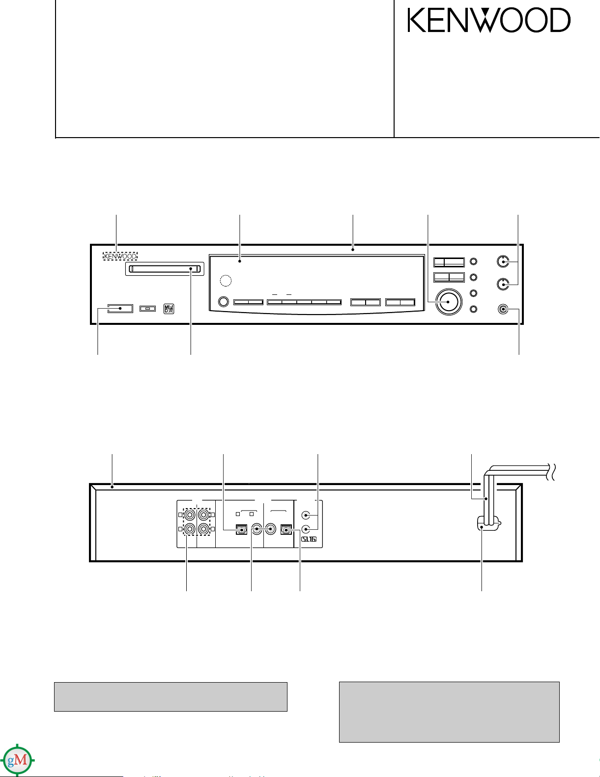
DISC LOADING MECHANISM
PHONES LEVEL
REC LEVEL
REC INPUT
REC MODE
/CHARA.
SET
ENTER
PHONES
STEREO MINIDISC RECORDER DM -5090
JOG DIAL
4
¢
1
37
8 
¡
MONITOR
AUTO/
MANU.
EDIT /
SPACE
DELETE
REPEAT
TITLE
SEARCHINPUT
TIME
DISPLAY
LEVEL
METER
MODE
0
TIMER
REC OFF PLAY
- ON – OFF
POWER
MIN MAX
MIN MAX
Dynamic Resolution Intensive Vector Enhancement
D.R.I.V.E.
STEREO MINIDISC RECORDER
1050MD/DM-5090
DM-9090
SERVICE MANUAL
1997-11/B51-5387-00 (K/K) 3191
©
KENWOOD badge*
(B43-)
Knob*
(K27-)
Metallic cabinet*
(A01-)
Panel*
(A29-)
Optic receiving module
(W02-1181-05)
Front glass*
(B10-)
Phono jack*
(E11-)
Panel*
(A60-)
Knob*
(K29-)
Knob*
(K29-)
Phone jack (3P)
(E11-0190-05)
AC power cord*
(E30-)
LINE
PLAY
REC
OUT
IN
L
R
R
R
L
R
Phono jack
(E63-0120-05)
In compliance with Federal Regulations, following are
reproductions of labels on, or inside the product relating to
laser product safety,
DIGITAL
REC
IN
2 COAX.1 OPT.
Phono jack*
(E63-)
PLAY
OUT
SYSTEM
CONTROL
OPT.COAX.
Oscillating module
(W02-1114-05)
Power cord bushing
(J42-0083-05)
Illustration is DM-5090.
*Refer to parts list on page 40.
KENWOOD-Corp. certifies this equipment conforms to
DHHS Regulation No.21 CFR 1040.10, Chapter 1,
Subchapter J.
DANGER : Laser radiation when open and interlock
defeated.
AVOID DIRECT EXPOSURE TO BEAM.
1050MD/DM-5090/DM-9090
N O DIS
C
CONTENTS/ACCESSORIES/CAUTIONS
CONTENTS
CONTENTS/ACCESSORIES/CAUTIONS...................2
EXTERNAL VIEW........................................................3
BLOCK DIAGRAM.......................................................4
CIRCUIT DESCRIPTION.............................................5
WIRING DIAGRAM....................................................14
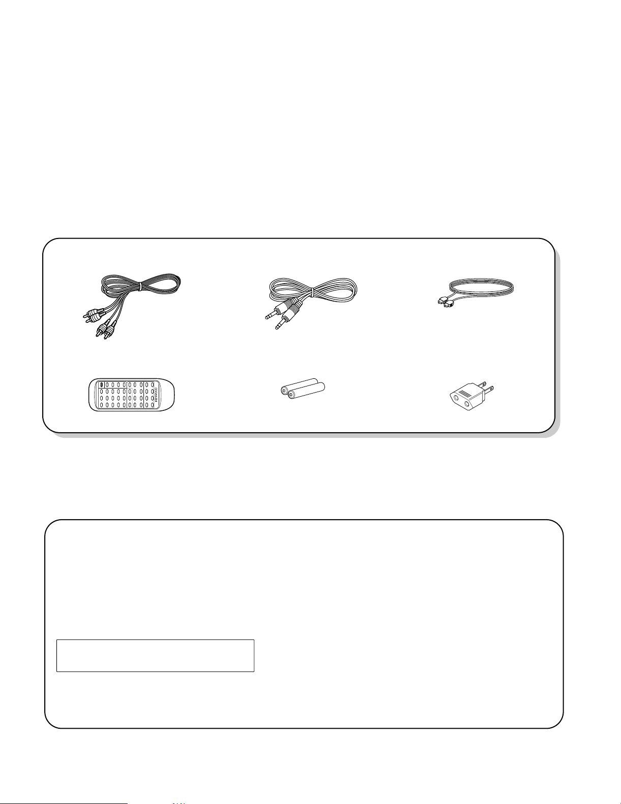
Accessories
PC BOARD ............................................................... 15
SCHEMATIC DIAGRAM........................................... 21
EXPLODED VIEW .....................................................37
PARTS LIST...............................................................40
SPECIFICATIONS.....................................................49
Audio cord (2)
(E30-0505-05)
Remote control unit (1)
(A70-1141-05: RC-M0702)
Battery cover: (A09-0362-08)
Cautions
Note related to transportation and movement
Before transporting or moving this unit, carry out the
following operation.
1. Set the POWER key to ON without loading a Mini Disc.
÷
Check that no disc is present in the unit.
2. Wait a few seconds and verify that the display shown
appear.
3. Set the POWER key to OFF.
System control cord (1)
(E30-2733-05)
Batteries (R6/AA) (2)
Beware of condensation
When water vapor comes into contact with the surface of
cold material, water drops are produced.
If condensation occurs, correct operation may not be possible, or the unit may not function correctly.
This is not a malfunction, however, the unit should be dried.
(To do this, turn the POWER switch ON and leave the unit
as it is for several hours.)
Be especially careful in the following conditions :
When the unit is brought from a cold place to a warm place,
and there is a large temperature difference.
When a heater starts operating.
When the unit is brought from an air-conditioned place to a
place of high temperature with high humidity.
When there is a large difference between the internal temperature of the unit and the ambient temperature, or in conditions where condensation occurs easily.
Optical fiber cable(1)
(B19-1529-05)
AC adaptor (1)
(E03-0115-05)
M type only
2
1050MD/DM-5090/DM-9090
EDIT/
SPACE
FADE/
DELETE
INPUT
MONITORREC INPUT
STEREO MINIDISC RECORDER DM-9090
TIMER
POWER
PHONES
- O N – OFF
LEVEL
MIN MAX
OFF
PLAYREC
SEARCH
TITLE
DISC LOADING MECHANISM
High bit Rec. & Play D.R.I.V.E.
20bit Rec. D.R.I.V.E. & 24 bit D/A converter
0
1 ¡
4 ¢
8 
7 3
ENTER
U PDOWN
PUSH SET
SEARCH
JOG DIAL
REC LEVEL REC BALANCE
MIN
L R
MAX
REC MODE
/CHARA.
R
L
SYSTEM
CONTROL
PLAY
OUT
OPT.COAX.
REC
IN
3 COAX.1 COAX. 2 OPT.
D I G I T A L
L I N E
PLAY
OUT
REC
I N
R
L
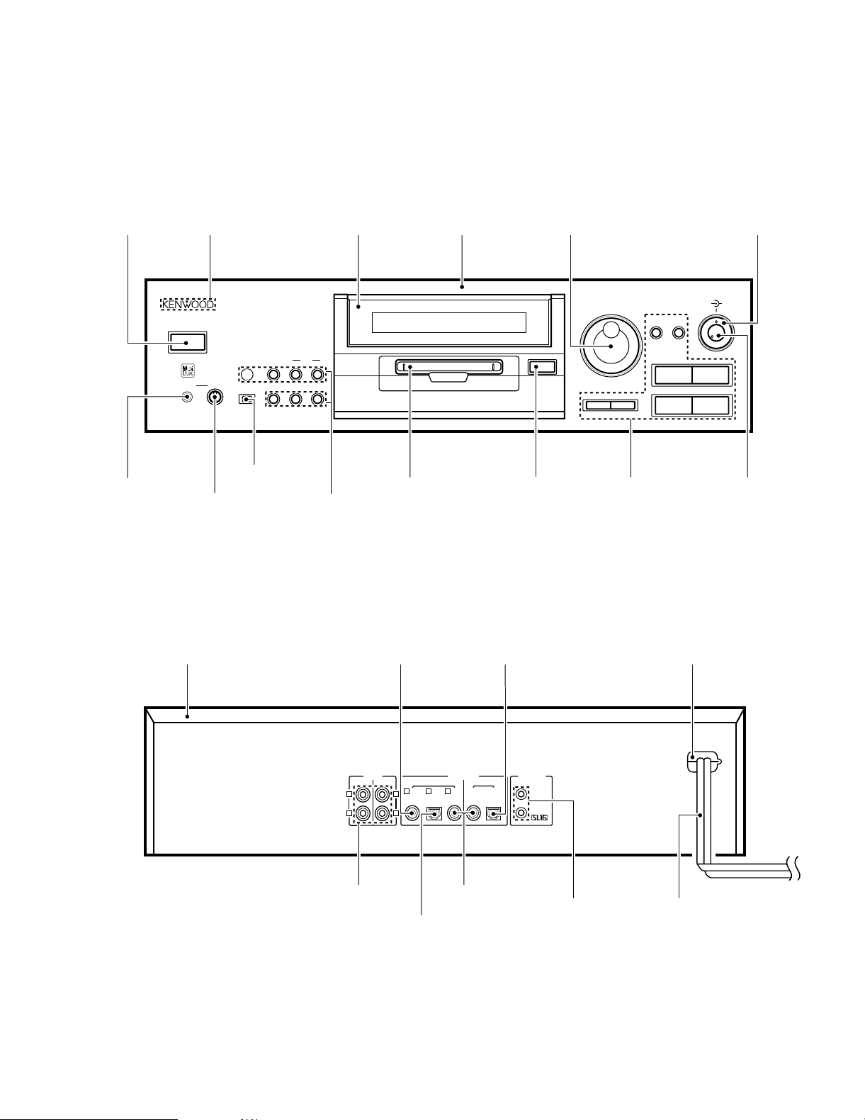
EXTERNAL VIEW
Knob
(K27-2178-04)
Phone jack (3P)
(E11-0190-05)
KENWOOD badge
(B43-0302-04)
Knob
(K29-6697-04)
Knob
(K29-3741-04)
Front glass
(B10-2362-04)
Escutcheon
(B07-2348-21)
Panel Assy
(A60-1258-02)
Panel
(A29-0868-24)
Knob
(K29-6700-03)
Escutcheon
(B07-2348-21)
Escutcheon
(B07-2361-22)
Knob
(K29-6695-14)
Knob
(K29-6692-04)
Metallic cabinet
(A01-3450-01)
Phono jack
(E63-0185-05)
Phono jack
(E63-0121-05)
Optic receiving module
(W02-1181-05)
Oscillating module
(W02-1114-05)
Phono jack
(E63-0174-05)
Miniature phone jack
(E11-0188-05)
Power cord bushing
(J42-0083-05)
AC power cord*
(E30-)
Illustration is DM-9090.
*Refer to parts list on page 40.
3
4
DM-9090(T,E)
DM-5090(J,K,M,T,E)2-71: DM-5090(T,E)
0-21: DM-5090(M)
0-00: DM-5090(J,K)
X00-285X-XX
X00-2842-71: DM-9090
X32-3470-00: DM-9090 ONLY
X25-5940-XX -02: DM-5090(J) -12: DM5090(K,M,T,E)
X25-5940-11: DM-5090(T,E)
X14-4430-00: DM-5090
X14-4380-00: DM-9090
MECHA: MDM-04 (X33-1100-00)
ANALOG
(J) TYPE ONLY
256fS
SENSOR
SUB-CODE
ONLY
4Mx1
3.3V
-
+
DM-5090
DM-5090
IC14
NON REG: 12V
5.03.3
DIGITAL
HEAD DRIVER
DIGITAL
256K SRAM
2
E PROM
IC27 LC89170M
CD TEXT
DECODER
3.35.0
5.0
REMOTE
CONTROL
RECORDING
HEAD
IC181
DIGITAL
DIGITAL
DIGITAL
EXCEPT
DM-5090
EXCEPT (K) TYPE
FL AC
-33V
u-COM +5V
u-COM VDD
AC
TEMP. DET.
IC26
ONLY
DM-5090
IC6
IC8 CS5335
DIGITAL
OUTPUT
INPUT
DIGTAL
SL16
SYSTEM
CONTROL
(K) TYPE
CONTROL
SYSTEM
TITLER
CYBER
OPT OUT
COAX. OUT
OPT IN
EXCEPT
DM-5090
COAX. IN 2
COAX. IN 1
IN/OUT
ANALOG
IN
ANALOG
ANALOG
OUT
PHONES
TA8409S
DRIVER
LOADING MOTOR
IC35
DISC
MOTOR
DISC
LASER DRIVE APC
Q162
DM-9090 ONLY
RECEIVER
INTERFACE
DIGITAL
IC14
DM-5090 ONLY
512fS
~
DIGITAL
ANALOG
ANALOG ANALOG
MOTOR
FEED
LOADING MOTOR
3.3
DIGITAL+5V
+3.3V
REG.
IC37
BUFFER
EXP.
I/O
IC32
DISC IN SW
START LIMIT SW
PROTECT SW
REFRECT SW
REC SW
REC LEVEL
JOG
REC BAL.
IC2
TIMER SW
MATRIX
KEY
IC1
DRIVER
FL DOT MATRIX
LC7571ONE
FIP12XM1GA
FL
KMS-260A
PICK UP
IC124
DRAM
PLAY POS. SW
IC152
IC121
DRIVER
MOTOR
(BH6511FP)
SERVO
IC101
RF AMP
(CXA2523R)
(CXA2523R)
MEMO. CONT
ATRAC
SERVO
DSP
ACIRC
SRAM +5V
+5V
DIGITAL HEAD MOTOR
ANALOG +5V AVR
AVR
AVR
AVR
LINE
FILTER
TRANSFORMER
POWER
IC31
IC28
256K SRAM
TITLER
& CD TEXT
u-COM
UPD78F4216
u-COM
MAIN
512fS
D/A CONV.
D.R.I.V.E.
with
KAN05SM5842 IC7-14IC5IC4
1/2
D.P.A.C.
D/A CONV.
24bit
RESOLUTION
DIGITAL FILTER
20bit(24bit)
IC23 LC8904Q
IC24 KAN03
D.R.I.V.E.
IC25 SM5844AF
CONVERTER
RATE
SAMPLING
DET.
DATA
DEMOD.
A/D CONV.
20bit
-VFL
FCS
TRK
AC
SYSTEM
AUDIO
FCS,TRK,SPIN,SLED PWM
FEED
SPINDLE
A,B,C,D,E,F
I,J,
APC REF
CONT,BUS
RF,TE,FE,SE
M
M
M
1050MD/DM-5090/DM-9090
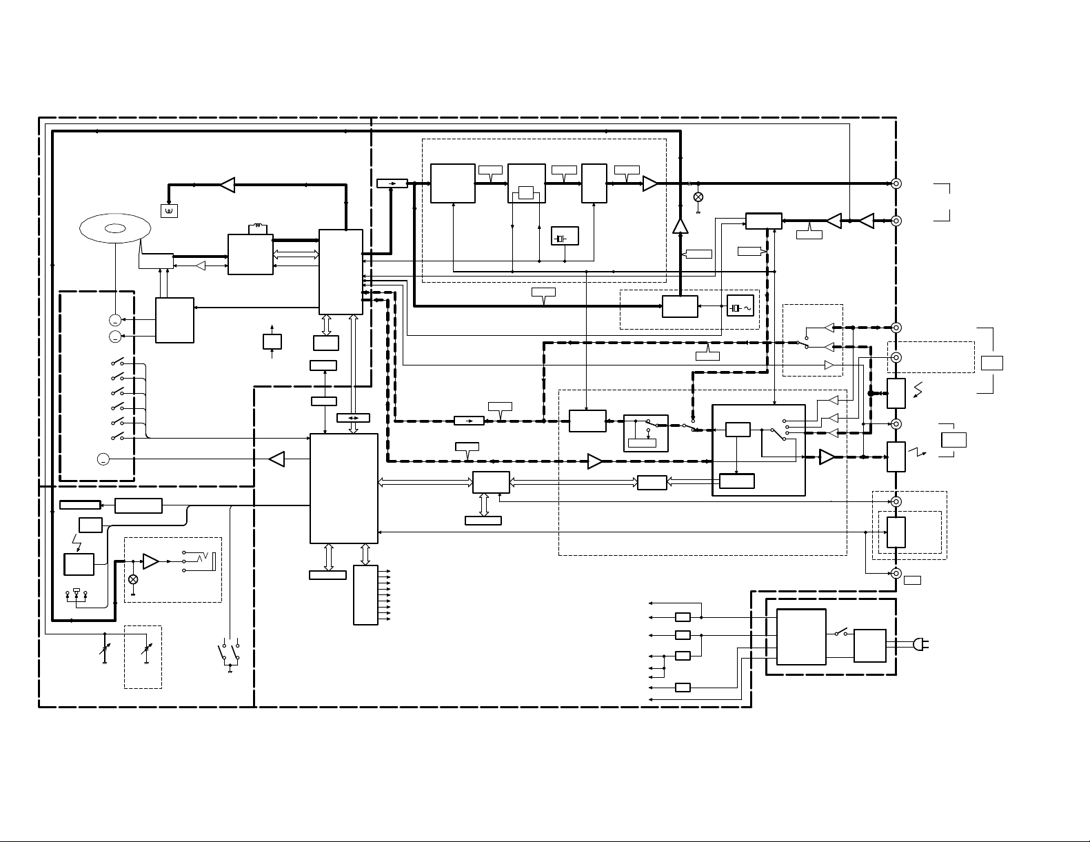
BLOCK DIAGRAM

1050MD/DM-5090/DM-9090
CIRCUIT DESCRIPTION
1. Mechanism microprocessor : uPD784215GF508 (X25- , IC31)
1-1 Pin description
No. Name I/O Description
1,2 - O N.C.
3 EXLAT O Output port of latch signal to IC32 (TC74HC4094)
4 EXCK O Clock output port to IC32 (TC74HC4094)
5 RD O SRAM WR
6 WR O SRAM WR
7 CS O SRAM CS L; SRAM enable
8 STB O Output port of strobe signal to IC33
9 Vdd - Power supply (Microprocessor)
10 POWER O Power terminal H; Power ON
11 MUTE O Mute control output L; Mute ON
12 INISW2 I Destination selector
13 SCHNG O E2PROM data IN/OUT change-over H; SDA output
14 SBUSY I/O 16 serial busy
15 SDATA I/O 16 serial data
16 SCL O Output port of clock signal to IC6 (X33)
17 SDA I/O Interface port of data signal from / to IC6 (X33)
18 LDON O Laser ON / OFF control port H; LD ON
19 RMS O Pick RMS H; ON
20 XLAT O System IC latch
21 SENS I System IC sens
22 GND - GND
23 PROTECT I Detection port of protect switch L; Protect ON
24 REFLECT I Detection port of reflect switch H; Low reflect
25 DISCIN I Detection of disc input switch L; Disc out SW ON
26 STTLMT I Detection port of limit switch L; Start limit SW ON
27 PHOTSW I Detection of mechanism play position L; Photo sensor ON
28 REC SW I Input port of detection from REC position switch L; REC SW ON
29 LOADIN O Output port of loading motor control signal L; Loading OUT
30 LOADOUT O Output port of loading motor control signal L; Loading IN
31 MNT0 I FOK signal from CXD2652AR (IC2) L; Focus ON
32 MNT2 I Input port of monitor 2 from CXD2652AR (IC2)
33 XRST O Output port of reset signal to CXD2652AR (IC2)
34 TX O Output port of recording permitted signal
35 RECP O Laser power control to CXD2652AR (IC2)
36 MNT3 I Input port of monitor 3 from CXD2652AR (IC2)
37 Vdd - Power supply (Microprocessor)
38,39 - Clock IN / OUT (12.5MHz)
40 GND - GND
41 OPEN O No used
42 GND I No used
5

1050MD/DM-5090/DM-9090
CIRCUIT DESCRIPTION
No. Name I/O Description
43 RESET I Microprocessor hard reset
44 REM I Remocon signal input terminal
45 XINT I Input port of interrupted status from CXD2652AR (IC2)
46 CE I Microprocessor chip enable H; Enable / L; disable
47 SQSY I Input port of sub code Q from CXD2652AR (IC2)
48 DQSY I U-bit of digital IN / SUB Q sync input of CD format from CXD2652AR (IC2)
49 DDQSY I U-bit of digital IN / SUB Q sync input from LC8904Q (IC23)
50 MNT1 I Input port of track jump detection from CXD2652AR (IC2)
51 Vdd - Microprocessor power supply
52 +5V - A/D reference voltage (+5)
53~56 KR0~KR3 I Key return (KR0~KR3)
57 TMSW I Timer switch input
58 INISW1 I Detection selector
59 BACK I Back up voltage detection
60 ENCB I Rotary encoder B
61 GND - GND
62 BACK ON O Back up change control
63 ENCA I Rotary encoder A
64 +5V - D/A reference voltage (+5V)
65 SRDT I Data for reading input from CXD2652AR (IC2)
66 SWDT O Data for writing to CXD2652AR (IC2)
67 SCLK O Serial clock to CXD2652AR (IC2)
68 CRXD I Communication to sub u-COM (IC28)
69 CTXD O Communication to sub u-COM (IC28)
70 CENA I Communication to sub u-COM (IC28) H; Comm enable
71 EXDT O Data output to TC74HC4094 (IC32)
72 FLDCE O Chip enable to FL driver
73 DRDT I Read data from LC8904Q (IC23)
74 DWDT O Data to LC8904Q (IC23) and LC75710NE (IC1)
75 DCLK O Clock to LC8904Q (IC23) and LC75710NE (IC1)
76 DLAT O Latch to LC8904q (IC23)
77 DEMPH I Emphasis from LC8904Q (IC23)
78 DSUB1 I Sub 1 from LC8904Q (IC23)
79 DSUB2 I Sub 2 from LC8904Q (IC23)
80 SRCLAT O Latch to SM5844AF (IC25)
81 BACKCHK O Back up voltage check
82 VCLK O Clock to SM5844AF (IC25)
83 VLDT O Data to SM5844AF (IC25)
84~91 AD0~AD7 O SRAM address / data (AD0~AD7)
92~99 A8~A15 O SRAM address (A8~A15)
100 Vss - GND
6
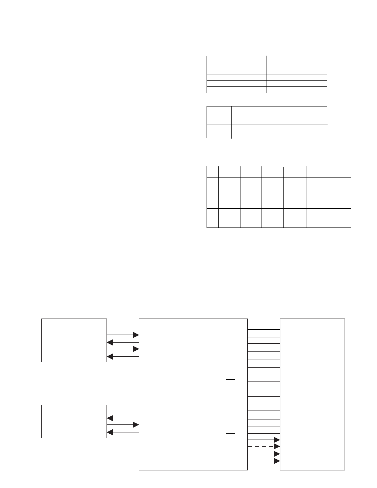
LC89170M
DQSY
SCLK
SRDT
XMODE
DQSY
SCLK
SRDT
XMODE
73
1
78
3
43
42
41
40
39
38
37
36
35
34
33
32
31
30
29
44
23
22
21
ADDRESS
/DATA
BUS
ADDRESS
BUS
ASTB
RD
WR
CS
51
50
49
MTXD
MRXD
MENA
CRxD
CTxD
CENA
MAIN u-COM
uPD784215GF
-508
uPD7804035GC
IC29,IC30
HM62256BLFP-8
T/-7T/-12T
[SRAM]
TC74HC373AF
X25- IC28 (Except DM-5090,K-type)
Titler & CD text
Sub - u-COM
IC27 (Except DM-5090)
IC31
1050MD/DM-5090/DM-9090
CIRCUIT DESCRIPTION
1-2. Initialization
POWER = ON (DM-9090,DM-5090)
REC INPUT = ANALOG
AUTO/MANUAL = AUTO
FADE = OFF
PLAY MODE = TRACK
REPEAT = OFF
TIME DISPLAY = SINGLE(+)
LEVEL METER MODE = NORMAL MODE
DIGITAL REC LEVEL = 0dB
AUTO TNO TIME = 2 sec
AUTO TNO LEVEL = 3 (-50dB)
FADE TIME = 3 sec
REC END WRITE = ON
DRIVE = ON
PRESET TITLE = PRE1 : Pops
PRE2 : Rock
PRE3 : Classic
PRE4 : Jazz
PRE5 : Disco
PRE6 : Best Hits
PRE7 : Air Check
PRE8 : No.
PRE9 : Vol.
1-3. Switch control table
INI SW1
AVref(0.8~1.0AVref) Mecha. u-COM MODE
0.7AVref(0.6~0.8AVref) -
0.5AVref(0.4~0.8AVref) DMF-7002S (J type)
0.3AVref(0.2~0.4AVref) DM-9090
0.0AVref(0.0~0.2AVref) DM-5090
(AVref=Vdd)
INI SW2
High Overseas : No katakana character
: No cyber titler
Low Japan : Katakana character
: Cyber titler
1-4. Key voltage matrix
0.00V 0.80V 1.61V 2.41V 3.22V 4.00V
~0.78V ~1.59V ~2.39V ~3.20V ~3.98V ~4.98V
KR0 POWER EJECT PAUSE - FF KR1 STOP REC PLAY - FB TT
SEARCH
KR2 DEL SPACE TT. REC. MONI TIME
/EDIT INPUT INPUT -TOR DISP
LEVEL
KR3 SET ENTER CHR AUTO / METER REPEAT
/ REC MANUAL MODE
2. Sub microprocessor : uPD784035GC (X25- ,IC28)
2-1. Sub microprocessor periphery block diagram
7

1050MD/DM-5090/DM-9090
CIRCUIT DESCRIPTION
2-2 Pin description (uPD784035GC)
No. Name I/O Description
1 SCLK O Text data read clock
2 N.C. O No used
3 XMODE O Text data decoder reset L: Power Down
4~6 N.C. O No used
7 RESET I Reset signal input
8 Vdd - Microprocessor power supply
9,10 X2,1 - 12.5MHz oscillator
11 Vss - GND
12~20 N.C. O No used
21 CS O Chip select for SRAM control H: Power Down
22 WR O Write strobe for SRAM control
23 RD O Read strobe for SRAM control
24~27 N.C. O No used
28 A15 O No used
29~35 A14~A8 - SRAM control terminal (address BUS), A14~A8
36~43 D7~D0 - SRAM control terminal (address / data BUS) , D7~D0
44 STB O Address strobe signal output
45,46 GND - GND
47,48 N.C. O No used
49 CENA O Communication to main u-COM (enable)
50 CTXD I Communication to main u-COM (uart TXD)
51 CRXD O Communication to main u-COM (uart RXD)
52~55 N.C. O No used
56 Vdd - Microprocessor power supply
57~61 N.C. I GND
62 CTR I Cyber titler (J type only)
63 TXT I CD text (J type only)
64 Avdd - A/D power supply terminal (+5V)
65 AVref1 - A/D reference voltage
66 AVss - A/D GND
67,68 N.C. O No used
69 AVref2 - D/A reference voltage
70 AVref3 - D/A GND
71,72 N.C. I Noused
73 DQSY I Text data reading permitted terminal L: Interrupt
74~77 N.C. I No used
78 SRDT I Text data reading line
79 RXD I Communication to cyber titler (UART) (J type only)
80 TXD O Communication to cyber titler (UART) (J type only)
8
1050MD/DM-5090/DM-9090
CIRCUIT DESCRIPTION
3. Test mode of the unit
3-1 Setting of the test mode
While pressing the [STOP] key, plug the AC power cord
into the AC wall outlet.
3-2 Contents of the test mode
1 [DOT TEST]
2 [SEG TEST]
✜3 [KEY TEST]
✜4 [CYBER TEST] J type only
✜Used for production line only
3-3 Function of the test mode
1 [DOT TEST]
The FL display starts the "NIAGARA MODE" by pressing
the [SET] key in the [DOT TEST] mode.
2 [SEG TEST]
Turn the FL indication ON by pressing the [SET] key in
the [SEG TEST] mode.
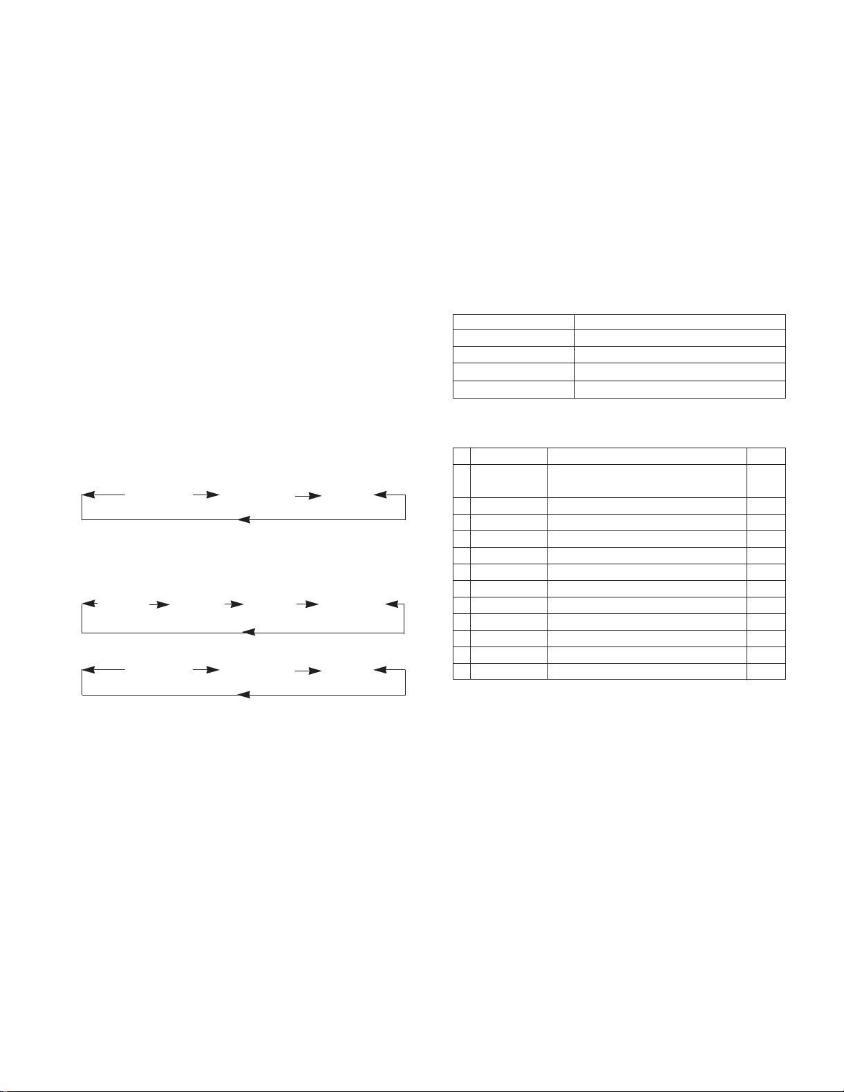
The FL indication changes cyclically as shown in the
below by turning the JOG DIAL (4¢).
FL LIGHT ON FL LIGHT OFF ENGLISH
3-4 Function of the key
1 JOG UP (¢) and JOG DOWN (4)keys
: Selects the test mode.
[DOT TEST] [SEG TEST] [KEY TEST] [CYBER TEST]
: Selects the FL indication
FL LIGHT ON FL LIGHT OFF ENGLISH
4. Mechanism test mode
4-1 Setting the test mode
Connect a plug of AC power cord to an outlet of AC, while
pressing PLAY key.
4-2 Canceling the test mode
Unplug the AC power cord.
4-3 Basic operation in test mode
All operations are performed using the JOG DIAL
(up/down), ENTER key, DELETE key, and SET key. The
functions of each key are shown in the table below.
Function Description
JOG DIAL(up/down) Changes the parameter and mode.
ENTER key Proceeds for definition.
DELETE key Returns for interrupt.
SET key Skip the mode and go to next step.
4-4 Selection of test mode
12 test modes are selected by turning the JOG DIAL.
No. Display Description Section
1 TEMP ADJUST The work of adjustment is unnecessary -
in this mode
2 LDPWR ADJUST Laser power adjustment 5-5
3 LDPWR CHECK Laser power check 5-5
4 EFBAL ADJUST Traverse adjustment 5-6
5 FBIAS ADJUST Focus bias adjustment 5-7
6 CPLAY MODE Continuous playback mode 4-4-1
7 CREC MODE Continuous recording mode 4-4-2
8 STT-LIMIT SW Check the mechanism start limit SW position 9 JUMP MODE Track jump checking mode -
10 SRV DAT READ Servo data reading 11 EEP MODE E2PPROM data reading or rewrite 12 EEP INITIAL E2PROM data initializing -
2 Set key
: Proceeds the test mode or return to test mode.
3 Stop key
: Cancel the test mode.
3-5 Microprocessor reset
The microprocessor can be initialized while pressing the
[EJECT] key, plug the AC power cord into the AC wall
outlet.
For more information on each adjustment mode, refer to
each section of 5, “Electrical adjustment”.
If other adjustment mode has been entered incorrectly,
press the DELETE key to exit the mode.
* The number 8 - 12 are not used for service. If these
mode have been entered incorrectly, press the DELETE
key immediately to exit the mode. Specially, do not use
EEP INITIAL. (E2PROM data has initialized if used it.)
4-4-1 Operation in continuous playback mode
1. Entering the continuous playback mode
(1) Insert a recordable disc or pre-mastered disc into the
unit.
(2) Turn the JOG DIAL to display “CPLAY MODE”.
(3) Press the ENTER key. The display then changes from
“CPLAY MODE” to “CPLAY MID”.
(4) After the access operation is completed, the display
changes from “CPLAY MID” to “C=#### a=##”.
Note: Numerals on the display appear the error rate and
ADIP error.
9
1050MD/DM-5090/DM-9090
CIRCUIT DESCRIPTION
2. Change the playback point.
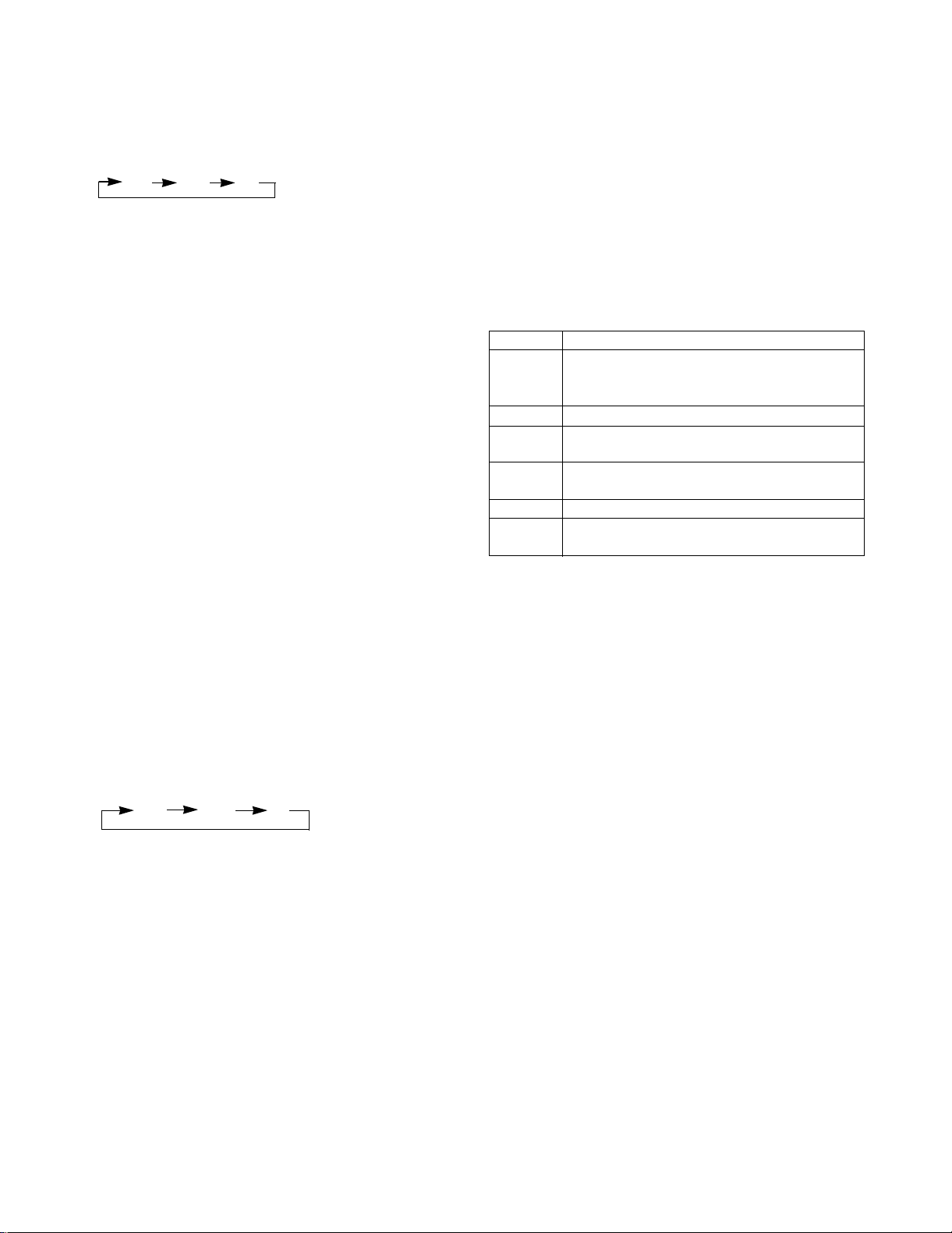
(1) Press the ENTER key during continuous playback. The
display then changes as follows.
MID OUT IN
(2) After the access operation is completed, the display
changes “C=####” a=##”.
Note: Numerals on the display appear the error rate and
ADIP error.
3. Terminating the continuous playback mode
(1) Press the DELETE key. The display then changes to
“CPLAY MODE”.
(2) Press the EJECT key to take out the disc.
Note : The playback start addresses of IN, MID, and OUT
are described below.
IN 30H cluster
MID 300H cluster
OUT 700H cluster
4-4-2 Operation in continuous recording mode
1. Entering the continuous recording mode
(1) Insert a recordable disc into the unit.
(2) Turn the JOG DIAL to display “CREC MODE”.
(3) Press the ENTER key. The display then changes from
“CREC MODE” to “CREC IN”.
(4) Press the ENTER key again. The display changes from
“CREC IN” to “CREC (####)”, and the continuous
recording is started.
Note: Numerals on the display (####) appear the address of
recording point.
2. Change the recording point.
(1) Turn the JOG DIAL to clockwise while “CREC IN” is dis-
played. The display changes as follows. (The recording
point can be shifted.)
MID OUT IN
(2) Press the ENTER key. The display then changes to
“CREC(####)”, and the continuous recording is started.
Note : Numerals on the display (####) appear the address
of recording point.
3. Terminating the continuous recording mode
(1) Press the DELETE key. The display then changes to
“CREC MODE” and the REC display goes off.
(2) Press the EJECT key to take out the disc.
Notes :
1. The recording start addresses of IN, MID, and OUT are
described below.
IN 30H cluster
MID 300H cluster
OUT 700H cluster
2. The DELETE key can be pressed at any time to stop the
recording.
3. An erasure prevention control is not detected in the test
mode. Be careful not to enter the continuous recording
mode using a disc containing the data that should not be
erased.
4. Do not record continuously for more than five minutes.
5. Take care that no vibration is applied during continuous
recording.
4-5 Other key functions
Function Description
3 Plays back continuously when this key is pressed during
stop. Turn on and off the tracking servo when it is
pressed during continuous playback.
7 Stops the continuous playback and recording.
1 The thread moves to the inner circumference while this key
is pressed.
REC INPUT Selects the mode for the pit and groove every time this key
is pressed.
REC MODE Selects the spindle servo mode. (CLV-S and CLV-A)
TITLE INPUT Selects the contents of the display every time this key
is pressed.
Note : An erasure prevention control is not detected in the
test mode. Notice that recording is performed irrespective
of the erasure prevention control position when the REC key
is pressed.
4-6 Display in test mode
The display is selected in the order of MODE display,
address display and error rate display every time the TITLE
INPUT key is pressed.
1. MODE display
“TEMP ADJUST” and “CPLAY MODE” are displayed as the
MODE display.
2. Error rate display
The error rare display appears as described below.
C1 = #### AD = ##
C1 = C1 error,AD = ADIP error
3. Address display
The address display appears as described below.
h = ####, d = ####(Recordable groove and pre-mastered
disc.)
h=Header address, d=ADIP address
* When no address can be read," - " display appears.
4. Segment indication
[play] mark : servo on
[pause] mark : tracking servo on
[rec] mark : servo on (laser light power)
[SINGLE] : servo groove mode
[TOTAL] : servo mode (CLV-A)
[PGM] : spindle lock
[COPY] : recordable disc
10
1050MD/DM-5090/DM-9090
CIRCUIT DESCRIPTION
4-7 Precaution on use of test mode
✜ An erasure prevention control is not detected in the test
mode. Therefore, when the recording laser power mode
such as continuous recording mode and traverse adjustment mode is entered, the contents of the existing recording are erased irrespective of the control position. Be careful not to enter the continuous recording mode and traverse
adjustment mode when using a disc, containing the data
that should not be erased, in the test mode.
5. Electrical adjustment
5-1 Precaution during confirmation of Laser Diode
emission
During adjustment, do not view the emission of a laser diode
from just above for confirmation. This may damage your eyes.
5-2 Precaution on handling of Optical pick-up (KMS-
260A)
The laser diode in an optical pick-up is easy to be subject to
electrostatic destruction. Therefore, solder-bridge the laser tap
on the flexible board when handling the optical pick-up.
When removing the flexible board from the connector, make a
solder bridge in advance, then remove the board. Be careful
not to remove the solder bridge before inserting the connector.
Moreover, take careful measures against electrostatic destruction. The flexible board is cut easily. Handle the flexible board
with care.
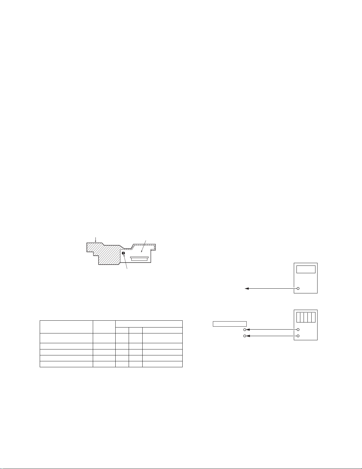
Pick-up
Flexible board
5) Take care that VC and GND (ground) are not connected
on the oscilloscope when two or more signals are monitored on the oscilloscope. (VC and GND are short-circuited in this case.)
Note : The "#" display on the screen indicates an arbitrary
figure.
5-4 Creating the recordable continuous recording
disc
This disc is used for focus bias adjustment and error rate
confirmation. How to create the recordable continuous
recording disc is described below.
1. Insert a commercial recordable disc (blank disc).
2. Turn the JOG DIAL to display “CREC MODE.”
3. Press the ENTER key to display “CREC IN”.
4. Turn the JOG DIAL (CW ) to display “CREC-MID”.
5. After pressed the ENTER key, a display indicates
“CREC(0300)” and the recording begins.
6. Terminate the recording within five minutes.
7. Press the DELETE key to stop the recording.
8. Press the EJECT key to take out the recordable disc.
As a result, a continuously recorded disc can be created for
focus bias adjustment and error rate confirmation.
Note : Take care that no vibration is applied during continu-
ous recording.
5-5 Laser power adjustment
Connection :
Laser
power meter
Laser tap
5-3 Precaution during adjustment
1) Perform the adjustment and confirmation marked with “O”
in the order shown in the table when the parts below are
replaced.
2) In the test mode, perform the adjustment. After adjustment
is completed, cancel the test mode.
Optical BD board
1.Temperature compen-
sation offset adjustment X O O O
2.Laser power adjustment O O X O
3.Traverse adjustment O O X O
4.Focus bias adjustment O O X O
5.Error rate confirmation O O X O
3) Perform the adjustment in the order described.
4) Use the following tools and measurement equipment.
• CD test disc TGYS-1
• Laser power meter
• Oscilloscope (with bandwidth of more than 40 MΩ)
(Calibrate the probe before measurement.)
• Digital voltmeter
• Thermometer
pick-up IC6 D101 IC1,IC2,IC10
Objective lens of
optical pick up
Digital
voltmeter
X33
ADJUSTMENT
TP2
TP1
Adjustment :
1. Put the laser power meter on the objective lens of the
optical pick-up. Connect the digital voltmeter to TP1 and
TP2.
2. Turn the JOG DIAL to display “LDPWR ADJUST”.
(Laser power : For adjustment use)
3. Press the ENTER key to display “(0.9mW)$##”.
4. Adjust to turn JOG DIAL so that the laser power meter
reads 0.86 - 0.94mW.
Set range 10mW of the laser power meter,then save to
press ENTER key.
5. “(7.0mW)$##” is displayed.
6. Adjust to turn the JOG DIAL so that laser power meter
reads 6.9-7.1mW, then save to press ENTER key.
("LDPWR<$##" is displayed monentarily.)
+
-
11
1050MD/DM-5090/DM-9090
In this case, lop = 82.5 mA
lop(mA) = Reading of digital voltmeter(mV)/1(Ω)
(optical pick-up label)
KMS
260A
27x40
B0825
TE2
VC
Oscilloscope
X33
ADJUSTMENT
+
-
V: 0.5V/div H: 10ms/div
INPUT: DC mode
CIRCUIT DESCRIPTION
✜ Don't output the laser power of 7.0mW more than 15sec.
7. Next turn the JOG DIAL to display "LDPWR CHECK".
8. Press ENTER key to display "(0.9mW)$##". Check the
laser power meter reads 0.85-0.95mW.
9. Next set range 10mW of the laser power meter, then
press ENTER key to display "(7.0mW)$##". Confirm that
the laser power meter and digital voltmeterat that time
read the specified value.
Specification :
Reading of laser power meter : 7.0 ±0.1 mW
Reading of digital voltmeter : Optical pick-up indication value
±10%
(Optical pick-up label)
In this case, lop = 82.5 mA
lop(mA) = Reading of digital voltmeter (mV)/1(Ω)
10.Press the ENTER key to display “LDPWR CHECK” and
stop the laser emission. (The DELETE key can be
pressed at any time to stop the laser emission.)
Note : The "#" display on the screen indicates an arbitrary
figure.
5-6. Traverse Adjustment
Connection :
6. Press the ENTER key to display "EFB=##XSAVE"
momentarily. After that, "EF=$##MOR" is displayed.
(Laser power READ power, focus servo ON, tracking
servo OFF, and spindle(S) servo ON.)
7. Turn the JOG DIAL so that the waveform on the oscilloscope satisfies the specified value. (When the JOG DIAL
is turned, the #-marked figure in "EF-##" changes and
the waveform also changes.) During this adjustment, the
oscilloscope changes in units of about 2%. Adjust so that
the waveform comes nearest to the specified value. (MO
groove read power traverse adjustment)
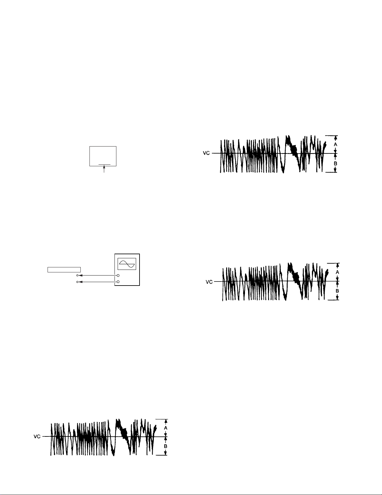
(Traverse waveform)
Specification : A = B
8. Press the ENTER key to display “EFB=##XSAVE”
momentarily and save the adjustment result in nonvolatile memory After that, "EFBAL MO-P" is displayed.
9. Press ENTER key to display "EF=$##MOP".(A pick-up
moves automatically to pit block area.)
10.Turn the JOG DIAL so that the waveform on the oscilloscope comes near to the specified value. During this
adjustment, the waveform changes in units of about 2%.
Adjust so that the waveform comes nearest to the specified value.
(Traverse waveform)
Adjustment :
1. Connect the oscilloscope to (TE2) and (VC) on the X33
board.
2. Insert a commercial recordable disc.
3. Turn the JOG DIAL to display “EFBAL ADJUST”.
4. Press the ENTER key to display “EFBAL MO-W” and
after that press the ENTER key again to display
"EF=$##MOW".
5. Turn the JOG DIAL so that the waveform on the oscilloscope satisfies the specified value. (When the JOG DIAL
is turned, the #-marked figure in "EF=$##" changes and
the waveform also changes.)During this adjustment, the
oscilloscope changes in units of about 3%. Adjust so
that the waveform comes nearest to the specified value.
(MO groove read power traverse adjustment)
(Traverse waveform)
Specification : A = B
12
Specification : A = B
11.Press the ENTER key to display “EFB=##XSAVE”
momentarily and save the adjustment result in nonvolatile memory. After that, “EFBAL CHANGE” is displayed. The disc rotation stops automatically.
Note : The "#" display on the screen indicates an arbitrary
figure.
12. Press the EJECT key to take out a recordable disc.
13.Insert test disc TGYS-1.
14.Press the ENTER key to display “EF=$##CD”. A servo
is established automatically.
15.Turn the JOG DIAL so that the waveform on the oscilloscope comes near to the specified value. During this
adjustment, the waveform changes in units of about 2%.
Adjust so that the waveform comes nearest to the specified value.
(Traverse waveform)
