

Page 1

S530 Parametric Test System
Test Subroutine Library User’s Manual
S530-907-01 Rev. A / September 2015
www.keithley.com
*PS53090701A*
S530-907-01A
A Greater Measure of Condence
A Tektr onix Company
Page 2

Test Subroutine Library
S530 Parametric Test System
User's Manual
© 2015, Keithley Instruments
Cleveland, Ohio, U.S.A.
All rights reserved.
Any unauthorized reproduction, photocopy, or use of the information herein, in whole or in part,
without the prior written approval of Keithley Instruments is strictly prohibited.
All Keithley Instruments product names are trademarks or registered trademarks of Keithley
Instruments. Other brand names are trademarks or registered trademarks of their respective
holders.
Document number: S530-907-01 Rev. A / September 2015
Page 3

Safety precautions
The following safety precautions should be observed before using this product and any associated instrumentation. Although
some instruments and accessories would normally be used with nonhazardous voltages, there are situations where hazardous
conditions may be present.
This product is intended for use by qualified personnel who recognize shock hazards and are familiar with the safety precautions
required to avoid possible injury. Read and follow all installation, operation, and maintenance information carefully before using
the product. Refer to the user documentation for complete product specifications.
If the product is used in a manner not specified, the protection provided by the product warranty may be impaired.
The types of product users are:
Responsible body is the individual or group responsible for the use and maintenance of equipment, for ensuring that the
equipment is operated within its specifications and operating limits, and for ensuring that operators are adequately trained.
Operators use the product for its intended function. They must be trained in electrical safety procedures and proper use of the
instrument. They must be protected from electric shock and contact with hazardous live circuits.
Maintenance personnel perform routine procedures on the product to keep it operating properly, for example, setting the line
voltage or replacing consumable materials. Maintenance procedures are described in the user documentation. The procedures
explicitly state if the operator may perform them. Otherwise, they should be performed only by service personnel.
Service personnel are trained to work on live circuits, perform safe installations, and repair products. Only properly trained
service personnel may perform installation and service procedures.
Keithley Instruments products are designed for use with electrical signals that are measurement, control, and data I/O
connections, with low transient overvoltages, and must not be directly connected to mains voltage or to voltage sources with high
transient overvoltages. Measurement Category II (as referenced in IEC 60664) connections require protection for high transient
overvoltages often associated with local AC mains connections. Certain Keithley measuring instruments may be connected to
mains. These instruments will be marked as category II or higher.
Unless explicitly allowed in the specifications, operating manual, and instrument labels, do not connect any instrument to mains.
Exercise extreme caution when a shock hazard is present. Lethal voltage may be present on cable connector jacks or test
fixtures. The American National Standards Institute (ANSI) states that a shock hazard exists when voltage levels greater than
30 V RMS, 42.4 V peak, or 60 VDC are present. A good safety practice is to expect that hazardous voltage is present in any
unknown circuit before measuring.
Operators of this product must be protected from electric shock at all times. The responsible body must ensure that operators
are prevented access and/or insulated from every connection point. In some cases, connections must be exposed to potential
human contact. Product operators in these circumstances must be trained to protect themselves from the risk of electric shock. If
the circuit is capable of operating at or above 1000 V, no conductive part of the circuit may be exposed.
Do not connect switching cards directly to unlimited power circuits. They are intended to be used with impedance-limited
sources. NEVER connect switching cards directly to AC mains. When connecting sources to switching cards, install protective
devices to limit fault current and voltage to the card.
Before operating an instrument, ensure that the line cord is connected to a properly-grounded power receptacle. Inspect the
connecting cables, test leads, and jumpers for possible wear, cracks, or breaks before each use.
When installing equipment where access to the main power cord is restricted, such as rack mounting, a separate main input
power disconnect device must be provided in close proximity to the equipment and within easy reach of the operator.
For maximum safety, do not touch the product, test cables, or any other instruments while power is applied to the circuit under
test. ALWAYS remove power from the entire test system and discharge any capacitors before: connecting or disconnecting
cables or jumpers, installing or removing switching cards, or making internal changes, such as installing or removing jumpers.
Do not touch any object that could provide a current path to the common side of the circuit under test or power line (earth)
ground. Always make measurements with dry hands while standing on a dry, insulated surface capable of withstanding the
voltage being measured.
Page 4
For safety, instruments and accessories must be used in accordance with the operating instructions. If the instruments or
accessories are used in a manner not specified in the operating instructions, the protection provided by the equipment may be
impaired.
Do not exceed the maximum signal levels of the instruments and accessories, as defined in the specifications and operating
information, and as shown on the instrument or test fixture panels, or switching card.
When fuses are used in a product, replace with the same type and rating for continued protection against fire hazard.
Chassis connections must only be used as shield connections for measuring circuits, NOT as protective earth (safety ground)
connections.
If you are using a test fixture, keep the lid closed while power is applied to the device under test. Safe operation requires the use
of a lid interlock.
If a screw is present, connect it to protective earth (safety ground) using the wire recommended in the user documentation.
The symbol on an instrument means caution, risk of danger. The user must refer to the operating instructions located in the
user documentation in all cases where the symbol is marked on the instrument.
The symbol on an instrument means caution, risk of electric shock. Use standard safety precautions to avoid personal
contact with these voltages.
The symbol on an instrument shows that the surface may be hot. Avoid personal contact to prevent burns.
The symbol indicates a connection terminal to the equipment frame.
If this symbol is on a product, it indicates that mercury is present in the display lamp. Please note that the lamp must be
properly disposed of according to federal, state, and local laws.
The WARNING heading in the user documentation explains dangers that might result in personal injury or death. Always read
the associated information very carefully before performing the indicated procedure.
The CAUTION heading in the user documentation explains hazards that could damage the instrument. Such damage may
invalidate the warranty.
Instrumentation and accessories shall not be connected to humans.
Before performing any maintenance, disconnect the line cord and all test cables.
To maintain protection from electric shock and fire, replacement components in mains circuits — including the power
transformer, test leads, and input jacks — must be purchased from Keithley Instruments. Standard fuses with applicable national
safety approvals may be used if the rating and type are the same. Other components that are not safety-related may be
purchased from other suppliers as long as they are equivalent to the original component (note that selected parts should be
purchased only through Keithley Instruments to maintain accuracy and functionality of the product). If you are unsure about the
applicability of a replacement component, call a Keithley Instruments office for information.
To clean an instrument, use a damp cloth or mild, water-based cleaner. Clean the exterior of the instrument only. Do not apply
cleaner directly to the instrument or allow liquids to enter or spill on the instrument. Products that consist of a circuit board with
no case or chassis (e.g., a data acquisition board for installation into a computer) should never require cleaning if handled
according to instructions. If the board becomes contaminated and operation is affected, the board should be returned to the
factory for proper cleaning/servicing.
Safety precaution revision as of January 2013.
Page 5

General information .................................................................................................. 1-1
Table of Contents
Introduction .......................................................................................................................... 1-1
Manual contents ................................................................................................................... 1-1
Contact information .............................................................................................................. 1-1
Using the test subroutine library ............................................................................. 2-1
How to use the library reference .......................................................................................... 2-1
Categorized subroutine lists ................................................................................................. 2-2
Bipolar subroutines ................................................................................................................... 2-3
Resistors, diodes, capacitors, and special structure subroutines .............................................. 2-4
MOSFET subroutines ................................................................................................................ 2-4
FET and JFET subroutines ....................................................................................................... 2-5
Math and support subroutines ................................................................................................... 2-5
Test subroutine library reference ............................................................................ 3-1
Subroutine descriptions........................................................................................................ 3-1
beta1 ......................................................................................................................................... 3-1
beta2 ......................................................................................................................................... 3-3
beta2a ....................................................................................................................................... 3-4
beta3a ....................................................................................................................................... 3-6
bice ........................................................................................................................................... 3-8
bkdn .......................................................................................................................................... 3-9
bvcbo ...................................................................................................................................... 3-10
bvcbo1 .................................................................................................................................... 3-11
bvceo ...................................................................................................................................... 3-13
bvceo2 .................................................................................................................................... 3-14
bvces ....................................................................................................................................... 3-15
bvces1 ..................................................................................................................................... 3-16
bvdss ....................................................................................................................................... 3-17
bvdss1 ..................................................................................................................................... 3-19
bvebo ...................................................................................................................................... 3-20
cap .......................................................................................................................................... 3-21
deltl1 ....................................................................................................................................... 3-23
deltw1 ...................................................................................................................................... 3-24
ev ............................................................................................................................................ 3-25
fimv ......................................................................................................................................... 3-27
fnddat ...................................................................................................................................... 3-28
fndtrg ....................................................................................................................................... 3-29
fvmi ......................................................................................................................................... 3-29
gamma1 .................................................................................................................................. 3-31
gd ............................................................................................................................................ 3-32
gm ........................................................................................................................................... 3-34
ibic1 ......................................................................................................................................... 3-35
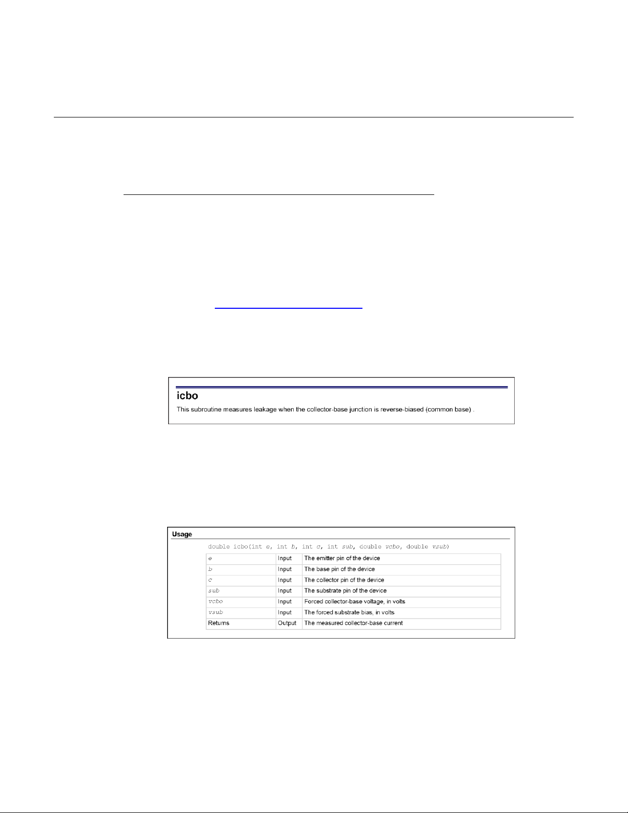
icbo ......................................................................................................................................... 3-37
iceo ......................................................................................................................................... 3-38
ices .......................................................................................................................................... 3-39
id1 ........................................................................................................................................... 3-40
idsat ........................................................................................................................................ 3-42
idss .......................................................................................................................................... 3-43
iebo ......................................................................................................................................... 3-44
idvsvg ...................................................................................................................................... 3-45
Page 6

Table of Contents S530 Parametric Test System Test Subroutine Library User's Manual
isubmx ..................................................................................................................................... 3-46
kdelay ...................................................................................................................................... 3-47
leak ......................................................................................................................................... 3-48
logstp ...................................................................................................................................... 3-49
rcsat ........................................................................................................................................ 3-50
re ............................................................................................................................................. 3-53
res ........................................................................................................................................... 3-55
res2 ......................................................................................................................................... 3-56
res4 ......................................................................................................................................... 3-57
resv ......................................................................................................................................... 3-58
rvdp ......................................................................................................................................... 3-59
tdelay ...................................................................................................................................... 3-60
tox ........................................................................................................................................... 3-61
vbes ........................................................................................................................................ 3-62
vf ............................................................................................................................................. 3-63
vg2 .......................................................................................................................................... 3-64
vgsat ....................................................................................................................................... 3-66
vp ............................................................................................................................................ 3-67
vp1 .......................................................................................................................................... 3-69
vt14 ......................................................................................................................................... 3-70
vtati ......................................................................................................................................... 3-71
vtext ........................................................................................................................................ 3-73
vtext2 ...................................................................................................................................... 3-76
vtext3 ...................................................................................................................................... 3-78
Index ........................................................................................................................... I-1
Page 7

In this section:
Introduction .............................................................................. 1-1
Manual contents ....................................................................... 1-1
Contact information .................................................................. 1-1
Section 1
General information
Introduction
The S530 Test Subroutine Library (PARLib) is a parameter extraction and data analysis software
system. The PARLib subroutines are used to analyze data associated with S530 parametric tests.
This manual contains detailed descriptions of the S530 PARLib subroutines. It is intended as a
reference guide for experienced users.
Manual contents
This manual is organized into the following sections:
General information: A definition of what the S530 Test Subroutine Library (PARLib) is, the
organization of the manual, and how you can contact us if you have questions.
Using the test subroutine library: Information about how the descriptions of the subroutines are
presented and a categorized list of the subroutines with links to the individual subroutine
descriptions.
Test subroutine library reference: Detailed information about each of the subroutines, in
alphabetical order. Descriptions include subroutine purpose, usage (syntax and parameters),
information about placement and relationship to other subroutines, and schematics (where
applicable).
Contact information
If you have any questions after you review the information in this documentation, please contact your
local Keithley Instruments office, sales partner, or distributor. You can also call Keithley Instruments
corporate headquarters (toll-free inside the U.S. and Canada only) at 1-800-935-5595, or from
outside the U.S. at +1-440-248-0400. For worldwide contact numbers, visit the Keithley website
(http://www.keithley.com).
Page 8
In this section:
How to use the library reference .............................................. 2-1
Categorized subroutine lists ..................................................... 2-2
Section 2
Using the test subroutine library
How to use the library reference
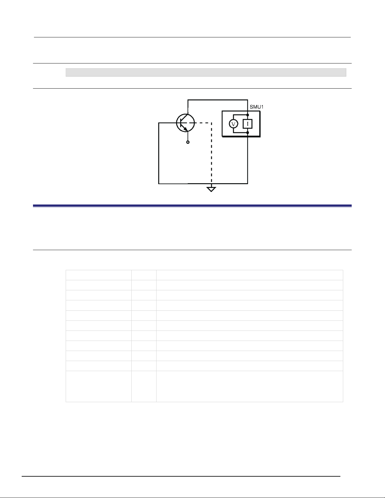
The subroutines in the Test subroutine library reference (on page 3-1) are in the C programming
language. Each subroutine is presented in a standard format that follows the pattern below:
Purpose statement: The first line of text under the subroutine heading contains a brief
explanation of what the subroutine does.
Figure 1: Example purpose statement
Usage: A line of code representing the prototype of the subroutine, followed by a table listing the
input and output parameters for the subroutine. Parameters that you specify are shown in
monospace italic font; parameters preceded by an asterisk (*) are pointers to information
that is returned. Each parameter is preceded by one of the following declarations that specifies
the data type for the parameter: int (integer), double (double-precision floating-point), and
char (a single character value).
Figure 2: Example syntax and parameter definition
Page 9
Section 2: Using the test subroutine library S530 Parametric Test System Test Subroutine Library User's Manual
2-2 S530-907-01 Rev. A / September 2015
Details: Additional information about using the subroutine.
Figure 3: Example details
V/I polarities: The polarities of the current or voltage flow between the pins of the device; based
on whether you are using an NPN or PNP transistor. This information is only applicable in some
subroutines.
Figure 4: Example V/I polarities information
Source-measure units (SMUs): A description of what each SMU in the test configuration does in
the subroutine. This information is only applicable in some subroutines.
Figure 5: Example SMUs description
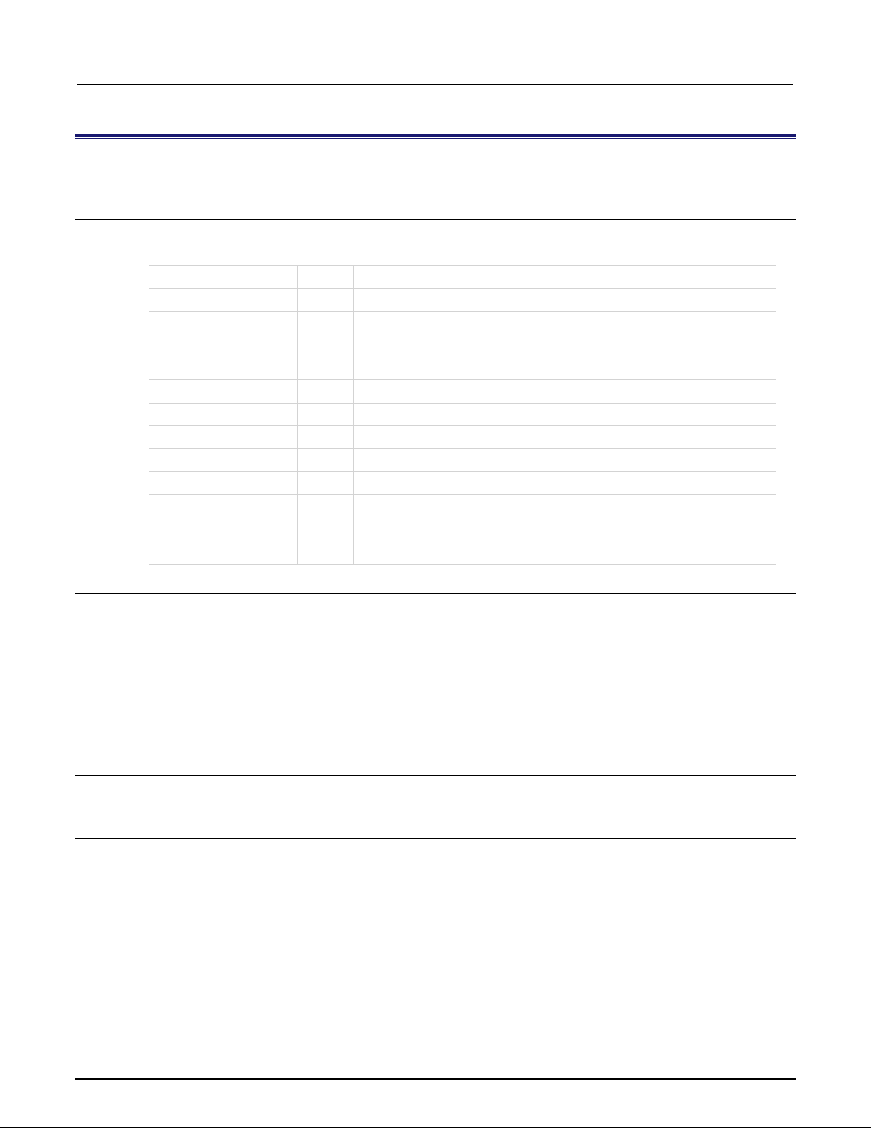
Schematic: A simplified schematic showing the configuration of the instruments and devices for
the subroutine. This information is only applicable in some subroutines.
Figure 6: Example schematic
Categorized subroutine lists
The subroutine descriptions are listed in alphabetical order in the Test subroutine library reference
(on page 3-1) section of this manual. The tables that follow contain all of the subroutines grouped by
function, with a brief description of the purpose of the subroutine and a hyperlink to the full subroutine
description.
Page 10
S530 Parametric Test System Test Subroutine Library User's Manual Section 2: Using the test subroutine library
S530-907-01 Rev. A / September 2015 2-3
Bipolar subroutines
Subroutine
Description
Link
beta1
Calculate DC at specified IE and VCB
beta1 (on page 3-1)
beta2
Calculate DC and VBE at specified IC and
VCE
beta2 (on page 3-3)
beta2a
Calculate at VCB and ICE with search on IE
beta2a (on page 3-4)
beta3a
Calculate at VCE and ICE with search on IBE
beta3a (on page 3-6)
bice
Calculate when VBE swept, at VCE and V
SUB
bice (on page 3-8)
bvcbo
Measure collector-base breakdown voltage,
emitter open
bvcbo (on page 3-10)
bvcbo1
Measure collector-base breakdown voltage
using LPTLib bsweepv subroutine
bvcbo1 (on page 3-11)
bvceo
Measure collector-emitter breakdown voltage,
base open
bvceo (on page 3-13)
bvceo2
Measure collector-emitter breakdown voltage
using LPTLib bsweepv subroutine
bvceo2 (on page 3-14)
bvces
Measure collector-emitter breakdown voltage
bvces (on page 3-15)
bvebo
Measure emitter-base breakdown voltage,
collector open
bvebo (on page 3-20)
ibic1
Measure ICE, IBE and calculate at VCE, VBE,
V
SUB
ibic1 (on page 3-35)
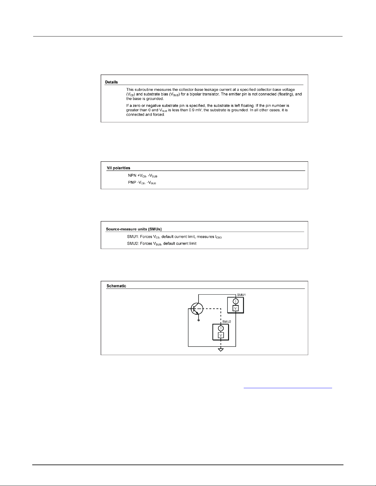
icbo
Measure collector-base leakage at VCB and
V
SUB
icbo (on page 3-37)
iceo
Measure collector-emitter leakage at VCE and
V
SUB
iceo (on page 3-38)
ices
Measure emitter-collector leakage at V
CES
and V
SUB
ices (on page 3-39)
iebo
Measure emitter-base leakage at VEB and
V
SUB
iebo (on page 3-44)
rcsat
Estimate rcsat when IC and IB swept at
constant
rcsat (on page 3-50)
re
Estimate emitter resistance
re (on page 3-53)
vbes
Measure base-emitter voltage at specified IE
(VC = VB)
vbes (on page 3-62)
Page 11

Section 2: Using the test subroutine library S530 Parametric Test System Test Subroutine Library User's Manual
2-4 S530-907-01 Rev. A / September 2015
Resistors, diodes, capacitors, and special structure subroutines
Subroutine
Description
Link
bkdn
Measure breakdown voltage (force I,
measure V)
bkdn (on page 3-9)
cap
Measure two-terminal capacitance
cap (on page 3-21)
fimv
Force current and measure voltage on device
with four high pins and four ground pins
fimv (on page 3-27)
fvmi
Force voltage and measure current on device
with four input pins and four ground pins
fvmi (on page 3-29)
leak
Measure leakage current at specified voltage
leak (on page 3-48)
res
2-terminal resistance (force I, measure V)
res (on page 3-55)
res2
2-terminal resistance with voltage limit
res2 (on page 3-56)
res4
4-terminal resistance (force I, measure V)
res4 (on page 3-57)
resv
2-terminal resistance (force V, measure I)
resv (on page 3-58)
rvdp
4-terminal van der Pauw measurement
rvdp (on page 3-59)
tox
Calculate oxide thickness from capacitance
tox (on page 3-61)
vf
Measure the forward junction voltage of a
diode
vf (on page 3-63)
Subroutine
Description
Link
bvdss
Measure drain-source breakdown voltage
(VG = 0)
bvdss (on page 3-17)
bvdss1
Measure drain-source breakdown voltage
using LPTLib bsweepv subroutine
bvdss1 (on page 3-19)
deltl1
Estimate delta L MOSFET parameter
deltl1 (on page 3-23)
deltw1
Estimate delta W for a MOSFET
deltw1 (on page 3-24)
gamma1
Estimate body effect ()
gamma1 (on page 3-31)
gd
Calculate drain conductance of a MOSFET
gd (on page 3-32)
id1
Measure drain current at specified VGS, VDS,
and VBS
id1 (on page 3-40)
idsat
Measure drain current at VDS, VBS (VD = VG)
idsat (on page 3-42)
idgsvg
Measure IDS when VGS is swept at constant
VDS and VBS
idvsvg (on page 3-45)
isubmx
Find peak substrate current at VDS,VBS
isubmx (on page 3-46)
vg2
Measure gate-source voltage at IDS, VDS, VBS
vg2 (on page 3-64)
vgsat
Measure V
GSAT
at specified IDS (VGS = VD)
vgsat (on page 3-66)
vt14
Estimate VT using two-point technique
vt14 (on page 3-70)
vtati
Find VT to produce specified IDS
vtati (on page 3-71)
vtext
Extrapolate gate-source threshold voltage
vtext (on page 3-73)
vtext2
Estimate VT using modified vtext subroutine
method
vtext2 (on page 3-76)
vtext3
Calculate VT using max slope method
vtext3 (on page 3-78)
MOSFET subroutines
Page 12
S530 Parametric Test System Test Subroutine Library User's Manual Section 2: Using the test subroutine library
S530-907-01 Rev. A / September 2015 2-5
FET and JFET subroutines
Subroutine
Description
Link
gm
Estimate MESFET transconductance at VDS,
VGS
gm (on page 3-34)
idss
Estimate MESFET I
DSS
and V
DSAT
at V
DSS
idss (on page 3-43)
vp
Estimate FET pinch-off voltage for a MESFET
vp (on page 3-67)
vp1
Estimate MESFET pinch-off at IDS (IP) and
VDS
vp1 (on page 3-69)
Subroutine
Description
Link
fnddat
Search an array, return a new array
fnddat (on page 3-28)
fndtrg
Determine which native mode trigger to use
fndtrg (on page 3-29)
kdelay
Delay, based on current and voltage values
kdelay (on page 3-47)
logstp
Create an array using logarithmic steps
logstp (on page 3-49)
tdelay
Return calculated delay time
tdelay (on page 3-60)
Math and support subroutines
Page 13
In this section:
Subroutine descriptions ............................................................ 3-1
e
Input
The emitter pin of the device
b
Input
The base pin of the device
c
Input
The collector pin of the device
sub
Input
The substrate pin of the device
ie
Input
The forced emitter current, in amperes
vcb
Input
The forced c to b bias, in volts
type
Input
Type of transistor: "N" or "P"
Returns
Output
The calculated beta of the device:
-1.0 = TYPE not "N" or "P"
-2.0 = SMU2 overload
-3.0 = Divide by 0, or < 0.01
-4.0 = > 10 K or I
B
wrong sign
-5.0 = Emitter voltage limit reached; developed emitter voltage is
within 98 % of the 3 V voltage limit
Section 3
Test subroutine library reference
Subroutine descriptions
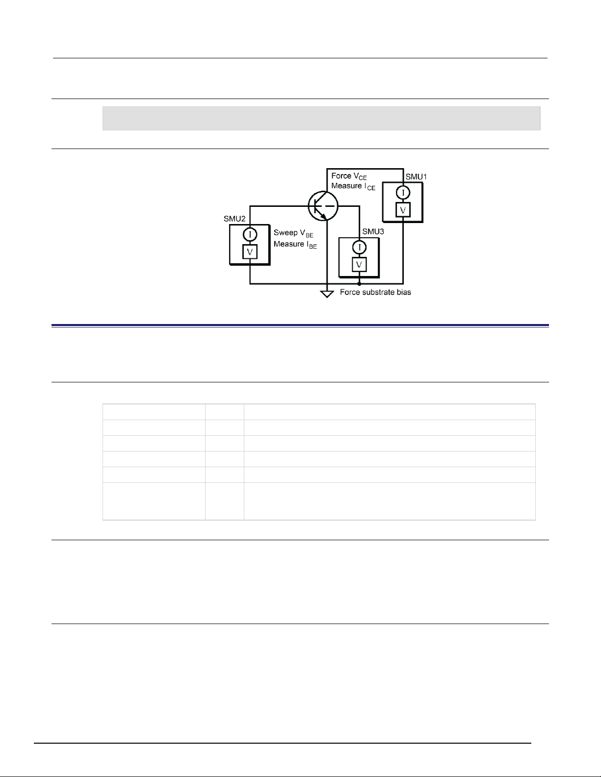
beta1
This subroutine calculates the DC beta () of a test device at constant emitter current (IE) and collector-base bias
(VCB). The device is in the common-base configuration.
Usage
double beta1(int e, int b, int c, int sub, double ie, double vcb, char type);
Details
If a positive substrate pin is specified, the substrate is grounded. If a positive substrate pin is not
specified, the substrate is left floating.
A delay is incorporated into the beta1 subroutine; this delay is the calculated time required for stable
forcing of emitter current with a 3 V voltage limit.
Page 14
Section 3: Test subroutine library reference S530 Parametric Test System Test Subroutine Library User's Manual
3-2 S530-907-01 Rev. A / September 2015
V/I polarities
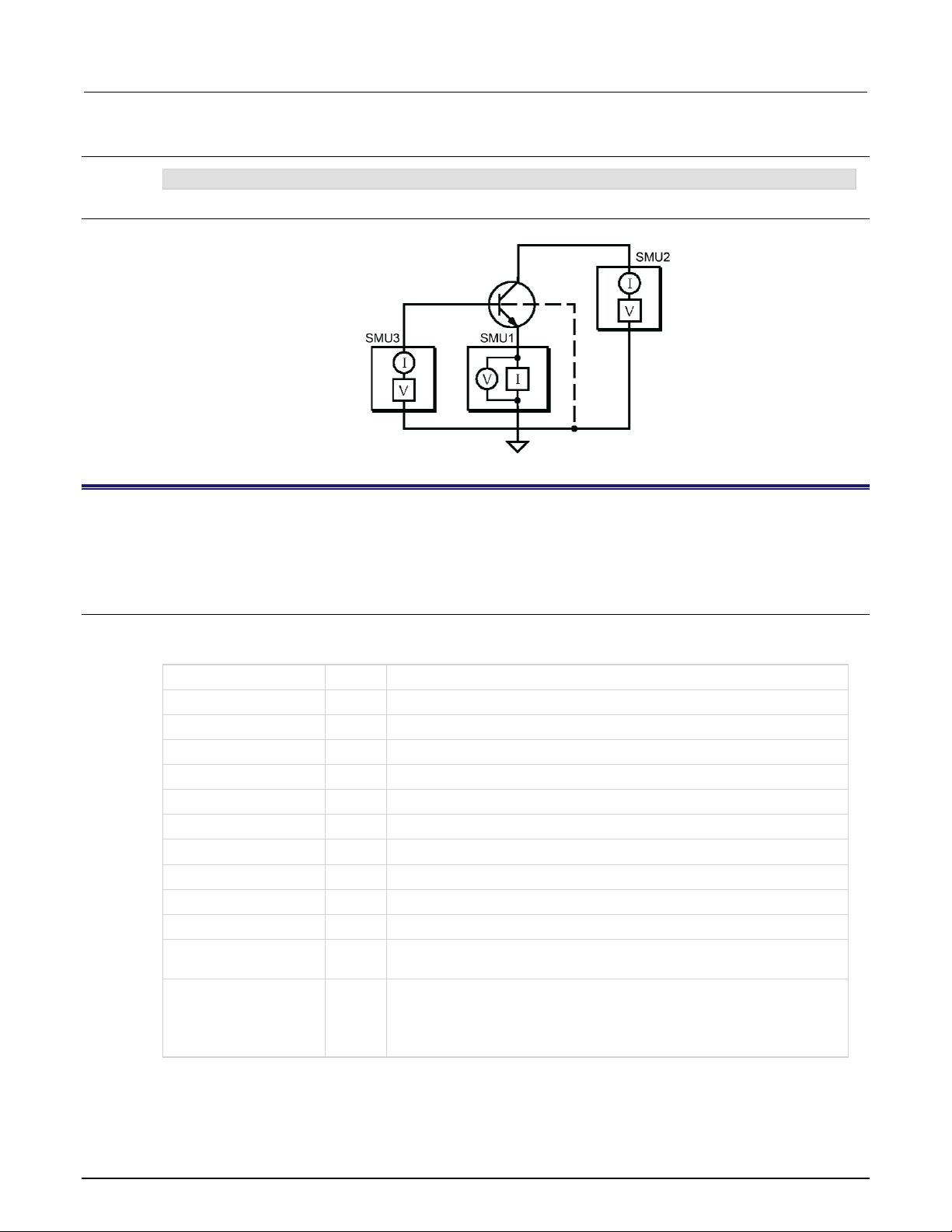
result = beta1(e, b, c, sub, ie, vcb, type);
Source-measure units (SMUs)
SMU1: Forces V
SMU2: Forces 0.0 V, measures base current (I
The polarities of VCB and IE are determined by device type.
Example
Schematic
SMU3: Forces I
, default current limit
CB
, 3 V voltage limit
E
)
B
Page 15
S530 Parametric Test System Test Subroutine Library User's Manual Section 3: Test subroutine library reference
S530-907-01 Rev. A / September 2015 3-3
beta2
e
Input
The emitter pin of the device
b
Input
The base pin of the device
c
Input
The collector pin of the device
sub
Input
The substrate pin of the device
ice
Input
The targeted collector current, in amperes
vce
Input
The forced collector-emitter voltage, in volts
type
Input
Type of transistor: "N" or "P"
vbeout
Output
The measured base voltage
icout
Output
The measured collector current
Returns
Output
The calculated beta:
-1.0 = TYPE not "N" or "P"
-2.0 = SMU2 overload
-3.0 = Divide by 0, or < 0.01
-4.0 = > 10 K
-5.0 = Too many iterations
-6.0 = Emitter voltage limit reached; developed emitter voltage is
within 98 % of the 3 V voltage limit
This subroutine calculates beta () and base-emitter voltage (VBE) at a specified collector current (IC) and
collector-emitter bias (VCE).
Usage
double beta2(int e, int b, int c, int sub, double ice, double vce, double *vbeout,
double *icout, char type);
Details
If a positive substrate pin is specified, the substrate is grounded. If a positive substrate pin is not
specified, the substrate is left floating.
A delay is incorporated into the beta2 subroutine; this delay is the calculated time required for stable
forcing of emitter current with a 3 V voltage limit.
A faster and simpler subroutine to use is beta2a (on page 3-4).
V/I polarities
The polarities of VCE and IE are determined by device type.
Source-measure units (SMUs)
SMU1: Forces I
SMU2: Forces V
SMU3: Forces 0.0 V, measures base current (I
, 3 V voltage limit
E
, maximum current limit, measures ICE
CE
)
B
Page 16
Section 3: Test subroutine library reference S530 Parametric Test System Test Subroutine Library User's Manual
3-4 S530-907-01 Rev. A / September 2015
Example
result = beta2 (e, b, c, sub, ice, vce, &vbeout, &icout, type);
e
Input
The emitter pin of the device
b
Input
The base pin of the device
c
Input
The collector pin of the device
sub
Input
The substrate pin of the device
ice
Input
The targeted collector current, in amperes
vcb
Input
The forced c to b bias, in volts
ie1
Input
The start of the emitter current search, in amperes
ie2
Input
The end of the emitter current search, in amperes
vsub
Input
The forced substrate bias, in volts
icmeas
Output
The final measured collector-emitter current
ieout
Output
The final forced value of emitter current
error
Output
The percent error between the target collector current (ICE) and the final
measured collector current (I
CMEAS
)
Returns
Output
The calculated beta:
-1.0 = Target ICE = 0.0
-2.0 = Collector current limit reached
-3.0 = Emitter voltage limit reached
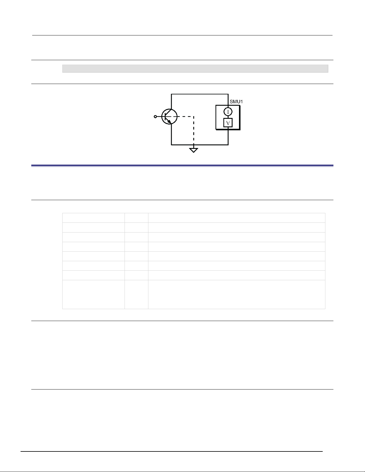
Schematic
beta2a
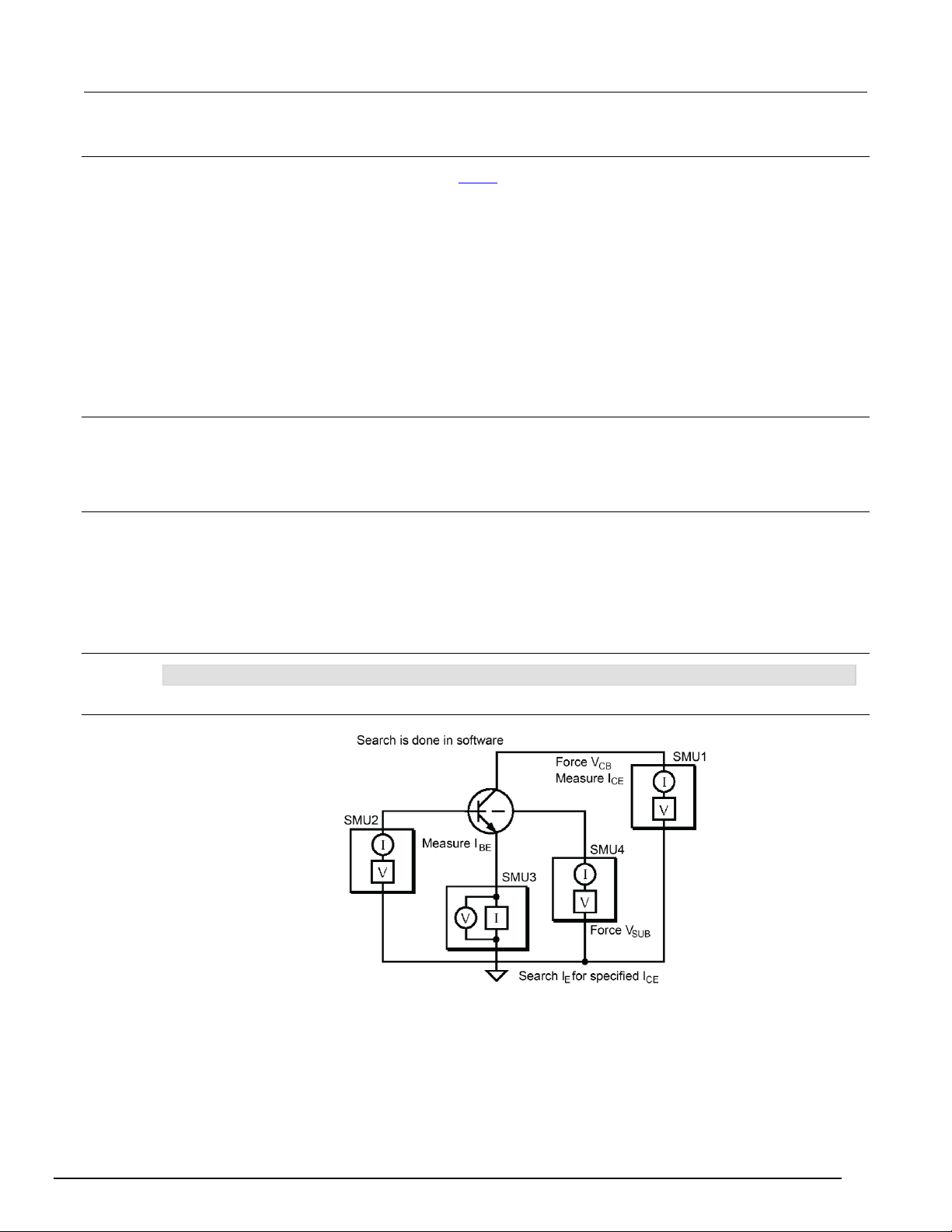
This subroutine calculates beta () at collector-base voltage (VCB) and collector-emitter current (ICE) using the
searchi and trig LPTLib functions to search emitter current (IE) until the target ICE is reached. The device is in
the common-base configuration.
Usage
double beta2a(int e, int b, int c, int sub, double ice, double vcb, double ie1,
double ie2, double vsub, double *icmeas, double *ieout, double *error);
Page 17
S530 Parametric Test System Test Subroutine Library User's Manual Section 3: Test subroutine library reference
S530-907-01 Rev. A / September 2015 3-5
Details
result = beta2a(e, b, c, sub, ice, vcb, ie1, ie2, vsub, &icmeas, &ieout, &error);
This subroutine is a revised version of the beta2 (on page 3-3) subroutine that uses the LPTLib
searchi and trig functions to search IE until the target ICE is reached.
This subroutine sets the current trigger on SMU1 at the specified ICE. The emitter current is searched
until the trigger is set. The emitter current is then forced, the collector current measured, and is
calculated.
The percent error (error) is calculated between the target ICE and the final measured ICE and
returned.
If a zero or negative substrate pin is specified, the substrate is left floating. If the pin number is
greater than 0 and V
connected and forced.
V/I polarities
is less than 0.9 mV, the substrate is grounded. In all other cases, it is
SUB
NPN +ICE, +VCB, IE, -V
PNP -ICE, -VCB, +IE, -V
Source-measure units (SMUs)
SMU1: Forces V
SMU2: Forces 0.0 V, measures I
SMU3: Searches I
Example
Schematic
SMU4: Forces V
SUB
SUB
, maximum current limit, triggers on ICE
CB
BE
, 3 V voltage limit
E
, default current limit
SUB
Page 18
Section 3: Test subroutine library reference S530 Parametric Test System Test Subroutine Library User's Manual
3-6 S530-907-01 Rev. A / September 2015
beta3a
e
Input
The emitter pin of the device
b
Input
The base pin of the device
c
Input
The collector pin of the device
sub
Input
The substrate pin of the device
ice
Input
The targeted collector current, in amperes
vce
Input
The forced collector-emitter voltage, in volts
ibe1
Input
The start of the base-emitter current (IBE) search, in amperes
ibe2
Input
The end of the base-emitter current (IBE) search, in amperes
vsub
Input
The forced substrate bias, in volts
ibe
Output
The final measured emitter-base current
icmeas
Output
The final measured collector-emitter current
error
Output
The percent error between the target collector current (ICE) and the final
measured collector current (I
CMEAS
)
Returns
Output
The calculated beta:
-1.0 = Target ICE = 0.0
-2.0 = Base voltage limit reached
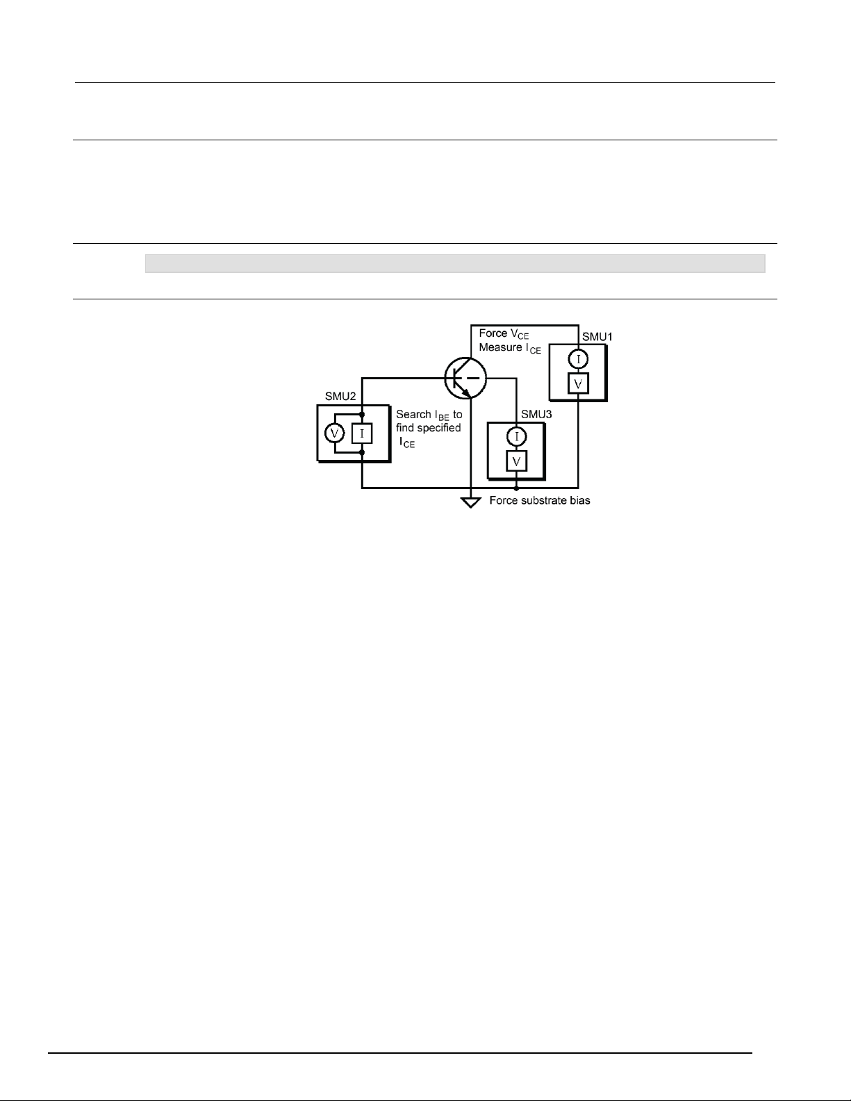
This subroutine calculates beta () at collector-emitter voltage (VCE) and collector-emitter current (ICE) using the
searchi and trig LPTLib functions to search base-emitter current (IBE) until the target ICE is reached. The
device is in the common-emitter configuration.
Usage
double beta3a(int e, int b, int c, int sub, double ice, double vce, double ibe1,
double ibe2, double vsub, double *ibe, double *cmeas, double *error);
Details
This subroutine sets the current trigger on SMU1 at the specified ICE. The base current is searched
until the trigger is set. The base current is then forced, the collector current measured, and is
calculated.
The percent error (error) is calculated between the target ICE and the final measured ICE and
returned.
If a zero or negative substrate pin is specified, the substrate is left floating. If the pin number is
greater than 0 and V
connected and forced.
V/I polarities
NPN +ICE, +VCE, +I
PNP -ICE, -VCE, -IBE, -V
is less than 0.9 mV, the substrate is grounded. In all other cases, it is
SUB
-V
SUB
SUB
BE,
Page 19
S530 Parametric Test System Test Subroutine Library User's Manual Section 3: Test subroutine library reference
S530-907-01 Rev. A / September 2015 3-7
Source-measure units (SMUs)
result = beta3a(e, b, c, sub, ice, vce, ibe1, ibe2, vsub, &ibe, &cmeas, &error);
Example
Schematic
SMU1: Forces V
SMU2: Searches I
SMU3: Forces V
, maximum current limit, triggers on ICE
CE
, 3 V voltage limit
BE
, default current limit
SUB
Page 20

Section 3: Test subroutine library reference S530 Parametric Test System Test Subroutine Library User's Manual
3-8 S530-907-01 Rev. A / September 2015
bice
e
Input
The emitter pin of the device
b
Input
The base pin of the device
c
Input
The collector pin of the device
sub
Input
The substrate pin of the device
vce
Input
The forced collector-emitter voltage, in volts
vbe1
Input
The start point of the VBE sweep, in volts
vbe2
Input
The end point of the VBE sweep, in volts
vsub
Input
Substrate bias, in volts
npts
Input
The number of points in the sweep
ice_last
Output
The measured ICE array
beta_last
Output
The calculated beta array
beta_max
Output
The maximum beta in the array
ic_max
Output
The ICE at maximum beta
This subroutine sweeps the emitter-base voltage (VBE), measures the resulting collector-emitter current (ICE), and
calculates beta ()at each value of V
configuration.
Usage
void bice(int e, int b, int c, int sub, double vce, double vbe1, double vbe2,
double vsub, int npts, double ice_last, double *beta_last, double *beta_max,
double *ic_max);
for a bipolar transistor. The device is connected in the common-emitter
BE
Details
The collector-emitter voltage (V
In addition to the and I
maximum (ic_max) are returned.
If a zero or negative substrate pin is specified, the substrate is left floating. If the pin number is
greater than 0 and V
connected and forced.
V/I polarities
NPNs +VCE, +IBE, and -V
PNPs -VCE, -IBE, and -V
Source-measure units (SMUs)
SMU1: Forces V
SMU2: Sweeps V
SMU3: Forces V
) and the substrate voltage (V
CE
return arrays, the maximum (beta_max) and collector current at
CE
is less than 0.9 mV, the substrate is grounded. In all other cases, it is
SUB
SUB
SUB
, maximum current limit, measures ICE
CE
, maximum current limit, measures IBE
BE
, default current limit
SUB
) are held constant.
SUB
Page 21
S530 Parametric Test System Test Subroutine Library User's Manual Section 3: Test subroutine library reference
S530-907-01 Rev. A / September 2015 3-9
Example
result = bice(e, b, c, sub, vce, vbe1, vbe2, vsub, npts, ice_last, &beta_last,
&beta_max, &ic_max);
hi
Input
The HI pin of the device
lo
Input
The LO pin of the device
sub
Input
The substrate pin of the device
ipgm
Input
The forced current, in amperes
vlim
Input
The voltage limit, in volts
Returns
Output
The measured breakdown voltage:
+2.0E + 21 = Measured voltage is within 98 % of the specified voltage
limit
Schematic
bkdn
This subroutine forces a current and measures breakdown voltage on a two-terminal device.
Usage
double bkdn(int hi, int lo, int sub, double ipgm, double vlim);
Details
If a positive substrate pin is specified, the substrate is grounded. If a positive substrate pin is not
specified, the substrate is left floating.
A delay is incorporated into the bkdn subroutine; this delay is the calculated time required for stable
Source-measure units (SMUs)
forcing of ipgm within the vlim voltage limit.
SMU1: Forces ipgm, programmable voltage limit, measures breakdown voltage
Page 22

Section 3: Test subroutine library reference S530 Parametric Test System Test Subroutine Library User's Manual
3-10 S530-907-01 Rev. A / September 2015
Example
result = bkdn(hi, lo, sub, ipgm, vlim);
e
Input
The emitter pin of the device
b
Input
The base pin of the device
c
Input
The collector pin of the device
sub
Input
The substrate pin of the device
ipgm
Input
The forced collector-base current (ICB), in amperes
vlim
Input
The collector voltage limit, in volts
type
Input
Type of transistor: "N" or "P"
Returns
Output
Collector-base voltage:
-1.0 = TYPE not "N" or "P"
+2.0E + 21 = Voltage limit reached; measured voltage is within
98 % of the specified voltage limit (vlim)
Schematic
bvcbo
This subroutine forces a collector current (I
emitter open.
Usage
double bvcbo(int e, int b, int c, int sub, double ipgm, double vlim, char type);
Details
) and measures the collector-base breakdown voltage (VCB) with the
CBO
If a positive substrate pin is specified, the substrate is grounded. If a positive substrate pin is not
specified, the substrate is left floating.
A delay is incorporated into the bvcbo subroutine; this delay is the calculated time required for stable
forcing of ipgm within the vlim voltage limit.
V/I polarities
The polarity of ipgm is determined by the device type.
Source-measure units (SMUs)
SMU1: Forces I
, programmed voltage limit, measures bvcbo
CBO
Page 23
S530 Parametric Test System Test Subroutine Library User's Manual Section 3: Test subroutine library reference
S530-907-01 Rev. A / September 2015 3-11
Example
result = bvcbo(e, b, c, sub, ipgm, vlim, type);
e
Input
The emitter pin of the device
b
Input
The base pin of the device
c
Input
The collector pin of the device
sub
Input
The substrate pin of the device
vcbmin
Input
The starting collector-base voltage (VCB), in volts
vcbmax
Input
The ending VCB, in volts
nstep
Input
The number of voltage steps
ipgm
Input
The targeted collector-base current (ICB), in amperes
udelay
Input
Delay between VCB steps, in seconds
type
Input
Type of transistor: "N" or "P"
Returns
Output
Collector-base voltage:
-1.0 = TYPE not "N" or "P"
+1.0E + 21 = Device triggered on vcbmin
+2.0E + 21 = Device triggered on vcbmax
Schematic
bvcbo1
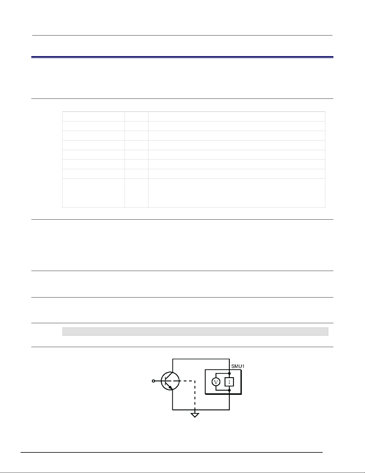
This subroutine uses the bsweepv LPTLib function to measure collector-base breakdown voltage at a specified
current with the emitter open.
Usage
double bvcbo1(int e, int b, int c, int sub, double vcbmin, double vcbmax, int
nstep, double ipgm, double udelay, char type);
Page 24
Section 3: Test subroutine library reference S530 Parametric Test System Test Subroutine Library User's Manual
3-12 S530-907-01 Rev. A / September 2015
Details
Result = bvcbo1(e, b, c, sub, vcbmin, vcbmax, nstep, ipgm, udelay, type);
This subroutine sweeps the collector-base voltage from vcbstart to vcbstop while monitoring the
collector current with the emitter open. When the programmed current level (ipgm) is reached, the
last collector-base voltage increment is returned as BVCBO1.
If a positive substrate pin is specified, the substrate is grounded. If a positive substrate pin is not
specified, the substrate is left floating.
The udelay parameter should be programmed to approximate c * vcbmax / ipgm, where c =
junction capacitance of the device under test.
V/I polarities
The polarities of vcbmin, vcbmax, and ipgm are determined by device type.
Source-measure units (SMUs)
Example
Schematic
SMU1: Forces V
, programmed current limit = 1.25 * ipgm, measures collector current (I
CB
CBO
)
Page 25
S530 Parametric Test System Test Subroutine Library User's Manual Section 3: Test subroutine library reference
S530-907-01 Rev. A / September 2015 3-13
bvceo
e
Input
The emitter pin of the device
b
Input
The base pin of the device
c
Input
The collector pin of the device
sub
Input
The substrate pin of the device
ipgm
Input
The forced collector-emitter current (ICE), in amperes
vlim
Input
The collector voltage limit, in volts
type
Input
Type of transistor: "N" or "P"
Returns
Output
Collector-emitter voltage:
-1.0 = TYPE not "N" or "P"
+2.0E + 21 = Voltage limit reached; measured voltage is within
98 % of the specified voltage limit (vlim)
result = bvceo(e, b, c, sub, ipgm, vlim, type);
This subroutine measures the collector-emitter breakdown voltage (VCE) when the collector current (IC) is forced
with the base terminal left open.
Usage
double bvceo(int e, int b, int c, int sub, double ipgm, double vlim, char type);
Details
If a positive substrate pin is specified, the substrate is grounded. If a positive substrate pin is not
specified, the substrate is left floating.
A delay is incorporated into the bvceo subroutine; this delay is the calculated time required for stable
forcing of ipgm within the vlim voltage limit.
V/I polarities
The polarity of ipgm is determined by the device type.
Source-measure units (SMUs)
SMU1: Forces I
Example
Schematic
, programmed voltage limit, measures bvceo
CEO
Page 26
Section 3: Test subroutine library reference S530 Parametric Test System Test Subroutine Library User's Manual
3-14 S530-907-01 Rev. A / September 2015
bvceo2
e
Input
The emitter pin of the device
b
Input
The base pin of the device
c
Input
The collector pin of the device
sub
Input
The substrate pin of the device
vcemin
Input
The starting collector-emitter voltage (VCE), in volts
vcemax
Input
The ending VCE, in volts
nstep
Input
The number of voltage steps
ipgm
Input
The targeted collector-emitter current (ICE), in amperes
udelay
Input
The delay between VCE steps, in seconds
type
Input
Type of transistor: "N" or "P"
Returns
Output
Collector-emitter voltage:
-1.0 = TYPE not "N" or "P"
+1.0E + 21 = Device triggered on vcemin
+2.0E + 21 = Device triggered on vcemax
This subroutine measures collector-emitter breakdown voltage using the bsweepV LPTLib function.
Usage
double bvceo2(int e, int b, int c, int sub, double vcemin, double vcemax, int
nstep, double ipgm, double udelay, char type);
Details
This subroutine sweeps VCE from vcemin to vcemax while monitoring the collector current with the
base open. When the specified current level (ipgm) is reached, the last collector-emitter voltage
increment is returned as bvceo2.
If a positive substrate pin is specified, the substrate is grounded. If a positive substrate pin is not
specified, the substrate is left floating.
Set the udelay parameter to approximate C * vcemax / ipgm, where C = Junction capacitance of
the device under test.
V/I polarities
The polarities of vcemin, vcemax, and ipgm are determined by device type.
Source-measure units (SMUs)
SMU1: Forces V
, programmed current limit = 1.25 *ipgm, measures I
CE
CEO
Page 27
S530 Parametric Test System Test Subroutine Library User's Manual Section 3: Test subroutine library reference
S530-907-01 Rev. A / September 2015 3-15
Example
result = bvceo2(e, b, c, sub, vcemin, vcemax, nstep, ipgm, udelay, type);
e
Input
The emitter pin of the device
b
Input
The base pin of the device
c
Input
The collector pin of the device
sub
Input
The substrate pin of the device
ipgm
Input
The forced I
CES
, in amperes
vlim
Input
The collector voltage limit, in volts
type
Input
Type of transistor: "N" or "P"
Returns
Output
Collector-emitter/base voltage:
-1.0 = TYPE not "N" or "P"
+2.0E + 21 = Voltage limit reached; measured voltage is within
98 % of the specified voltage limit (vlim)
Schematic
bvces
This subroutine measures the collector-emitter/base breakdown voltage by forcing a collector current (I
Usage
double bvces(int e, int b, int c, int sub, double ipgm, double vlim, char type);
Details
CES
).
This subroutine measures collector-to-emitter breakdown voltage at a specified current with the base
shorted to the emitter.
If a positive substrate pin is specified, the substrate will be grounded. If a positive substrate pin is not
specified, it is left floating.
A delay is incorporated into the bvces subroutine; this delay is the calculated time required for stable
forcing of ipgm within the vlim voltage limit.
V/I polarities
The polarity of ipgm is determined by the device type.
Page 28
Section 3: Test subroutine library reference S530 Parametric Test System Test Subroutine Library User's Manual
3-16 S530-907-01 Rev. A / September 2015
Source-measure units (SMUs)
resu1t = bvces(e, b, c, sub, ipgm, vlim, type);
e
Input
The emitter pin of the device
b
Input
The base pin of the device
c
Input
The collector pin of the device
sub
Input
The substrate pin of the device
vcemin
Input
The starting collector-emitter voltage (VCE), in volts
vcemax
Input
The ending VCE, in volts
nstep
Input
The number of voltage steps
ipgm
Input
The targeted collector-emitter current (ICE), in amperes
udelay
Input
The delay between VCE steps, in seconds
type
Input
Type of transistor: "N" or "P"
Returns
Output
Collector-emitter voltage:
-1.0 = TYPE not "N" or "P"
+1.0E + 21 = Device triggered on vcemin
+2.0E + 21 = Device triggered on vcemax
SMU1: Forces I
, programmed voltage limit, measures bvces
CES
Example
Schematic
bvces1
This subroutine measure the collector-emitter breakdown voltage using the bsweepV LPTLib function.
Usage
double bvces1(int e, int b, int c, int sub, double vcemin, double vcemax, int
nstep, double ipgm, double udelay, char type);
Page 29

S530 Parametric Test System Test Subroutine Library User's Manual Section 3: Test subroutine library reference
S530-907-01 Rev. A / September 2015 3-17
Details
result = bvces1(e, b, c, sub, vcemin, vcemax, nstep, ipgm, udelay, type);
d
Input
The drain pin of the device
g
Input
The gate pin of the device
s
Input
The source pin of the device
sub
Input
The substrate pin of the device
ipgm
Input
The forced drain current, in amperes
vlim
Input
The drain voltage limit, in volts
Returns
Output
Measured breakdown voltage:
+2.0E + 21 = Voltage limit reached; measured voltage is within
98 % of the specified voltage limit (vlim)
This subroutine sweeps the collector-emitter voltage from vcemin to vcemax while monitoring the
collector current with the base shorted to the emitter. When the programmed current level (ipgm) is
reached, the last collector-emitter voltage increment is returned as bvces1.
If a positive substrate pin is specified, the substrate is grounded. If a positive substrate pin is not
specified, the substrate is left floating.
Set the udelay parameter to approximate C * vcemax / ipgm, where C = Junction capacitance of
the device under test.
V/I polarities
Source-measure units (SMUs)
The polarities of vcemin, vcemax, and ipgm are determined by device type.
SMU1: Forces V
, programmed current limit = 1.25 *ipgm, measures I
CE
CEO
Example
Schematic
bvdss
This subroutine measure drain-source breakdown voltage (VG = 0) when the gate is grounded with the source.
Usage
double bvdss(int d, int g, int s, int sub, double ipgm, double vlim);
Page 30

Section 3: Test subroutine library reference S530 Parametric Test System Test Subroutine Library User's Manual
3-18 S530-907-01 Rev. A / September 2015
Details
result = bvdss(d, g, s, sub, ipgm, vlim);
This subroutine measures the drain-to-source breakdown voltage of a field-effect transistor (FET) with
the gate grounded with the source, at a specified current (magnitude and polarity).
If a positive substrate pin is specified, the substrate is grounded. If a positive substrate pin is not
specified, the substrate is left floating.
A delay is incorporated into the bvdss subroutine; this delay is the calculated time required for stable
forcing of ipgm within the vlim voltage limit.
V/I polarities
N-channel +Ipgm
Source-measure units (SMUs)
P-channel -Ipgm
SMU1: Forces ipgm, programmed voltage limit, measures bvdss
Example
Schematic
Page 31

S530 Parametric Test System Test Subroutine Library User's Manual Section 3: Test subroutine library reference
S530-907-01 Rev. A / September 2015 3-19
bvdss1
d
Input
The drain pin of the device
g
Input
The gate pin of the device
s
Input
The source pin of the device
sub
Input
The substrate pin of the device
vdsmin
Input
The starting drain-source voltage (VDS), in volts
vdsmax
Input
The ending VDS, in volts
nstep
Input
The number of voltage steps
ipgm
Input
Target drain-source current (VCS), in amperes
udelay
Input
The delay between VDS steps, in seconds
type
Input
Type of transistor: "N" or "P"
Returns
Output
Measured breakdown voltage:
-1.0 = TYPE not "N" or "P"
+1.0E+21 = Device triggered on vdsmin
+2.0E+21 = Device triggered on vdsmax
This subroutine measures the drain-source breakdown voltage using the bsweepv LPTLib function.
Usage
double bvdss1 (int d, int g, int s, int sub, double vdsmin, double vdsmax, int
nstep, double ipgm, double udelay, char type);
Details
This subroutine sweeps the drain-source voltage from vdsmin to vdsmax while monitoring the drain
current with the gate grounded to the source. When the specified current level (ipgm) is reached, the
last drain-source voltage increment is returned as bvdss1.
If a positive substrate pin is specified, the substrate is grounded. If a positive substrate pin is not
specified, the substrate is left floating.
Set the udelay parameter to approximate C * vdsmax / ipgm, where C = junction capacitance of
the device under test.
V/I polarities
The polarities of vdsmin, vdsmax, and ipgm are determined by device type.
Source-measure units (SMUs)
SMU1: Forces V
, programmed current limit = 1.25*ipgm, measures IDS
DS
Page 32

Section 3: Test subroutine library reference S530 Parametric Test System Test Subroutine Library User's Manual
3-20 S530-907-01 Rev. A / September 2015
Example
result = bvdss1(d, g, s, sub, vdsmin, vdsmax, nstep, ipgm, udelay, type);
e
Input
The emitter pin of the device
b
Input
The base pin of the device
c
Input
The collector pin of the device
sub
Input
The substrate pin of the device
ipgm
Input
The forced emitter-base current (IEB), in amperes
vlim
Input
The emitter voltage limit, in volts
type
Input
Type of transistor: "N" or "P"
Returns
Output
Emitter-base voltage:
-1.0 = TYPE not "N" or "P"
+2.0E + 21 = Voltage limit reached; measured voltage is within
98 % of the specified voltage limit (vlim)
Schematic
S
bvebo
This subroutine measures emitter-base breakdown voltage at a specified current with the collector open.
Usage
double bvebo(int e, int b, int c, int sub, double ipgm, double vlim, char type);
Details
This subroutine measures the emitter-base breakdown voltage by forcing an emitter current with the
collector pin open. Always call this subroutine last when testing transistors.
At high values of I
, degradation of the emitter-base junction can occur, which will lower beta ().
EBO
If a positive substrate pin is specified, the substrate is grounded. If a positive substrate pin is not
specified, the substrate is left floating.
A delay is incorporated into the bvebo subroutine; this delay is the calculated time required for stable
forcing of ipgm within the vlim voltage limit.
V/I polarities
The polarity of ipgm is determined by the device type.
Page 33

S530 Parametric Test System Test Subroutine Library User's Manual Section 3: Test subroutine library reference
S530-907-01 Rev. A / September 2015 3-21
Source-measure units (SMUs)
result = bvebo(e, b, c, sub, ipgm, vlim, type);
hi
Input
The HI pin of the device
lo
Input
The LO pin of the device
sub
Input
The substrate pin of the device
vbias
Input
The voltage bias on the device, in volts
Returns
Output
Measured capacitance
SMU1: Forces I
, programmed voltage limit, measures bvebo
EBO
Example
Schematic
cap
This subroutine measures the capacitance of a two-terminal device.
Usage
Details
double cap(int hi, int lo, int sub, double vbias);
This subroutine measures the capacitance of a two-terminal capacitor at a specified voltage. The
voltage is provided by the internal capacitance meter bias supply. The result is returned in farads.
If a positive substrate pin is specified, the substrate is grounded. If a positive substrate pin is not
specified, the substrate is left floating.
When using this routine for junction capacitance measurements, make sure the junction never
becomes forward biased. To prevent this, make sure the forward voltage is less than one-half the
barrier potential (for silicon, this means that the forward voltage (VF) should not exceed 300 mV to
350 mV).
At the onset of conduction in a forward-biased diode (V > 300 mV), the current flow causes
unpredictable readings in the capacitance meter (usually overrange, 1022).
Page 34

Section 3: Test subroutine library reference S530 Parametric Test System Test Subroutine Library User's Manual
3-22 S530-907-01 Rev. A / September 2015
Example
result = cap(hi, lo, sub, vbias);
Schematic
Page 35

S530 Parametric Test System Test Subroutine Library User's Manual Section 3: Test subroutine library reference
S530-907-01 Rev. A / September 2015 3-23
deltl1
d1
Input
The drain pin of Q1
g1
Input
The gate pin of Q1
s1
Input
The source pin of Q1
sub1
Input
The substrate pin of Q1
l1
Input
Drawn gate length of Q1, in microns
d2
Input
The drain pin of Q2
g2
Input
The gate pin of Q2
s2
Input
The source pin of Q2
sub2
Input
The substrate pin of Q2
l2
Input
Drawn gate length of Q2, in microns
vlow
Input
Start of the gate-source voltage (VGS) search, in volts
vhigh
Input
End of the VGS search, in volts
vds
Input
Drain bias, in volts
vbs
Input
Substrate bias, in volts
ithr
Input
Drain-source trigger current (IDS), in amperes
vstep
Input
VGS step size, in volts
npts
Input
Number of points in the VGS sweep
kflag
Output
Returned status flag:
0 = Normal completion
1 = First g
m
measurement failed
2 = Second g
m
measurement failed
Returns
Output
Estimated gate length reduction
This subroutine estimates MOSFET gate length reduction (L) using transconductance (gm) data obtained from
the vtext2 subroutine for two different transistors.
Usage
double deltl1(int d1, int g1, int s1, int sub1, double l1, int d2, int g2, int s2,
int sub2, double l2, double vlow, double vhigh, double vds, double vbs, double
ithr, double vstep, int npts, int *kflag)
Details
The npts parameter must be greater than 5. If a value less than 5 is used, the subroutine uses 5
points by default.
The equation used for this calculation is:
L = ((Slope1 / Slope2) (L1 - L2) / (Slope1 /Slope2 - 1.0)
Use this subroutine to infer the variability in the channel length based on the transconductance
comparison of two devices, where the reference device is considerably larger than the second device.
Page 36

Section 3: Test subroutine library reference S530 Parametric Test System Test Subroutine Library User's Manual
3-24 S530-907-01 Rev. A / September 2015
Source-measure units (SMUs)
Result = deltl1(d1, g1, s1, sub1, l1, d2, g2, s2, sub2, l2, vlow, vhigh, vds,
vbs, ithr, vstep, npts, &kflag)
d1
Input
The drain pin of Q1
g1
Input
The gate pin of Q1
s1
Input
The source pin of Q1
sub1
Input
The substrate pin of Q1
w1
Input
The drawn gate width of Q1, in microns
d2
Input
The drain pin of Q2
g2
Input
The gate pin of Q2
s2
Input
The source pin of Q2
sub2
Input
The substrate pin of Q2
w2
Input
The drawn gate width of Q2, in microns
vlow
Input
Start of the gate-source voltage (VGS) search, in volts
vhigh
Input
End of the VGS search, in volts
vds
Input
Drain bias, in volts
vbs
Input
Substrate bias, in volts
ithr
Input
Drain-source trigger current (IDS), in amperes
vstep
Input
VGS step size, in volts
npts
Input
Number of points in the VGS sweep
kflag
Output
Returned status flag:
0 = Normal completion
1 = First V
T
measurement failed
2 = Second V
T
measurement failed
Returns
Output
Estimated gate width reduction
See the vtext2 (on page 3-76) subroutine.
Example
deltw1
This subroutine estimates the gate width reduction parameter (W) for a MOSFET using two values of threshold
voltage (VT) obtained from the vtext2 subroutine.
Usage
double deltw1(int d1, int g1, int s1, int sub1, double w1, int d2, int g2, int s2,
int sub2, double w2, double vlow, double vhigh, double vds, double vbs, double
ithr, double vstep, int npts, int *kflag)
Page 37

S530 Parametric Test System Test Subroutine Library User's Manual Section 3: Test subroutine library reference
S530-907-01 Rev. A / September 2015 3-25
Details
result = deltw1(d1, g1, s1, sub1, w1, d2, g2, s2, sub2, w2, vlow, vhigh, vds,
vbs, ithr, vstep, npts, &kflag)
e
Input
The emitter pin of the device
b
Input
The base pin of the device
c
Input
The collector pin of the device
sub
Input
The substrate pin of the device
ibe
Input
Forced base current, in amperes
vstart
Input
The start of the collector-emitter voltage (VCE) sweep
vstop
Input
The end of the VCE sweep
npts
Input
The number of points in the sweep
vsub
Input
Substrate bias, in volts
slope
Output
The calculated inductance
iflag
Output
Status flag:
0 = Normal completion
1 = No valid data for fit
2 = Calculated slope = 0.0
3 = Developed base voltage is within 98 % of the 3 V voltage limit
r
Output
Correlation coefficient
early
Output
Calculated early voltage
W is calculated using the following equation:
L = ((Slope2 / Slope1) W1 - W2) / (Slope2 /Slope1 - 1.0)
The npts parameter must be greater than 5. If a value less than 5 is used, the subroutine uses 5
points by default.
Source-measure units (SMUs)
See the vtext2 (on page 3-76) subroutine.
Example
ev
This subroutine calculates the early voltage at constant base-emitter current (IBE).
Usage
void ev(int e, int b, int c, int sub, double ibe, double vstart, double vstop, int
npts, double vsub, double *slope, double *iflag, double *r, double *early);
Page 38

Section 3: Test subroutine library reference S530 Parametric Test System Test Subroutine Library User's Manual
3-26 S530-907-01 Rev. A / September 2015
Details
ev(e, b, c, sub, ibe, vstart, vstop, npts, vsub, &slope, &iflag, &r, &early);
This subroutine estimates the forward early voltage of a bipolar device at constant IBE. The device is
connected in the common-emitter configuration, and a collector-emitter voltage (VCE) and collectoremitter current (ICE) data set is generated. A linear least squares (LLSQ) line is fit to the data, and
the X-intercept is returned as the forward early voltage. The correlation coefficient is returned as an
estimate of the fit.
When calling this routine, make sure the VCE start and stop values have the device well into
saturation.
If a zero or negative substrate pin is specified, the substrate is left floating. If the pin number is
greater than 0 and V
connected and forced.
V/I polarities
NPN +VCE, +IBE and -VSUB
is less than 0.9 mV, the substrate is grounded. In all other cases, it is
SUB
Source-measure units (SMUs)
SMU1: Sweeps VCE, default current limit, measures ICE
SMU2: Forces ibe, 3 V voltage limit
PNP -VCE, -IBE and -VSUB
Example
Schematic
SMU3: Forces vsub, default current limit
Page 39

S530 Parametric Test System Test Subroutine Library User's Manual Section 3: Test subroutine library reference
S530-907-01 Rev. A / September 2015 3-27
fimv
h1
Input
HI pin 1
h2
Input
HI pin 2
h3
Input
HI pin 3
h4
Input
HI pin 4
l1
Input
LO pin 1
l2
Input
LO pin 2
l3
Input
LO pin 3
l4
Input
LO pin 4
v
Output
Measured voltage
i
Input
Forced current, in amperes
Returns
Output
Measured voltage:
0.0 = All high or low pins are <1
result = fimv(h1, h2, h3, h4, l1, l2, l3, l4, &v, i);
This subroutine forces a current and measures a voltage on a device with four high (source) pins and four ground
pins. This is an alternate version of the fvmi subroutine.
Usage
double fimv(int h1, int h2, int h3, int h4, int l1, int l2, int l3, int l4, double
*v, double i);
Details
Input a -1 if the pin is not to be used.
A delay is incorporated into the fimv subroutine; this delay is the calculated time required for stable
forcing of i with a 30 V voltage limit (default).
Source-measure units (SMUs)
SMU1: Forces current, default voltage limit, measures voltage
Example
Schematic
Figure 7: Schematic for the fimv subroutine
Page 40

Section 3: Test subroutine library reference S530 Parametric Test System Test Subroutine Library User's Manual
3-28 S530-907-01 Rev. A / September 2015
fnddat
x
Input
Input x array
npts
Input
Number of points in the input array
y
Input
Input y array
npts1
Input
Number of points in the input array
x1
Input
Minimum valid point
x2
Input
Maximum valid point
xnew
Output
Screened x array
np1
Input
Number of points in the output array
ynew
Output
Screened y array
npt2
Input
Number of points in the output array
np
Output
Number of points in the output array
code
Input
Search "x" or "y" data array
Returns
Output
The new array
fnddat(&x, npts, &y, npts1, x1, x2, &xnew, np1, &ynew, np2, &np, code)
This subroutine searches an array and returns a new array.
Usage
void fnddat(double *x, int npts, double *y, int npts1, double x1, double x2, double
*xnew, int np1, double *ynew, int np2, int *np, char code)
Details
Example
This subroutine searches a data set of x and y values for a specified range of data and returns two
new arrays with the screened data. Use this routine in other routines to remove unwanted or bad
points from measured data.
The x, y, xnew, and ynew parameters are all adjustable dimensioned arrays. The calling routine
should dimension them all the same.
The code parameter searches either the x data or y data. For example, in most measurement
routines, either the voltage or current is fixed, and the other variable is measured. The measured
variable is normally what is screened.
Page 41

S530 Parametric Test System Test Subroutine Library User's Manual Section 3: Test subroutine library reference
S530-907-01 Rev. A / September 2015 3-29
fndtrg
low
Input
The low value
high
Input
The high value
Returns
Output
TRUE = Use the Less Than trigger
FALSE = Use the Greater Than trigger
result = fndtrg(low, high)
h1
Input
HI pin 1
h2
Input
HI pin 2
h3
Input
HI pin 3
h4
Input
HI pin 4
l1
Input
LO pin 1
l2
Input
LO pin 2
l3
Input
LO pin 3
l4
Input
LO pin 4
v
Input
Forced voltage, in volts
i
Output
Measured current
Returns
Output
Measured current:
0.0 = All high or low pins are < 1
+4.0E+21 = Measured voltage is within 98 % of the default current
limit
This subroutine determines which native mode trigger to use.
Usage
int fndtrg(double low, double high)
Details
This subroutine compares the algebraic magnitudes of the input parameters and sets its return value
TRUE if TRIGL should be used or FALSE if TRIGH should be used.
Example
fvmi
This primitive subroutine forces a voltage and measures a current on a device with four input pins and four ground
pins.
Usage
double fvmi(int h1, int h2, int h3, int h4, int l1, int l2, int l3, int l4, double
v, double *i);
Details
This subroutine is normally used for defect structures with multiple high pins and ground pins.
Page 42

Section 3: Test subroutine library reference S530 Parametric Test System Test Subroutine Library User's Manual
3-30 S530-907-01 Rev. A / September 2015
Source-measure units (SMUs)
result = fvmi(h1, h2, h3, h4, l1, l2, l3, l4, v, &i);
Example
Schematic
SMU1: Forces voltage, default current limit, measures current
Figure 8: Schematic for the fvmi subroutine
Page 43

S530 Parametric Test System Test Subroutine Library User's Manual Section 3: Test subroutine library reference
S530-907-01 Rev. A / September 2015 3-31
gamma1
d
Input
The drain pin of the device
g
Input
The gate pin of the device
s
Input
The source pin of the device
sub
Input
The substrate pin of the device
vlow
Input
Low limit of the expected threshold
vhigh
Input
High limit of the expected threshold
vds
Input
Drain-source voltage, in volts
vbs1
First substrate to source voltage
vbs2
Second substrate to source voltage
phip
Surface potential, in volts
ithr
Drain-source trigger current (IDS), in amperes
vstep
Gate-source voltage (VGS) step size, in volts
npts
The number of points in the sweep
kflag
Output
Returned status flag:
0 = Normal completion
1 = First V
T
measurement failed
2 = second V
T
measurement failed
Returns
Output
Estimated body effect
This subroutine returns the value of the body effect parameter gamma obtained from two measurements of the
threshold voltage (VT) at different substrate bias voltages (VBS).
Usage
double gamma1(int d, int g, int s, int sub, double vlow, double vhigh, double vds,
double vbs1, double vbs2, double phip, double ithr, double vstep, int npts, int
*kflag)
Details
This subroutine estimates body effect from VT measured at two VBS values. The body effect
parameter characterizes the effect of the substrate bias on threshold voltage. The VT data is obtained
using the vtext2 subroutine.
The equation used in this subroutine:
= VT2-VT1/VT1 +p-VT2+p)
Where:
= MOSFET body effect constant
V
V
The npts parameter must be greater than 5. If a value less than 5 is used, the subroutine uses 5
points by default.
= Threshold voltage at the first value of VBS
T1
= Threshold voltage at the second value of VBS
T2
= Surface potential (twice the Fermi level)
p
Page 44

Section 3: Test subroutine library reference S530 Parametric Test System Test Subroutine Library User's Manual
3-32 S530-907-01 Rev. A / September 2015
Source-measure units (SMUs)
result = gamma1(d, g, s, sub, vlow, vhigh, vds, vbs1, vbs2, phip, ithr, vstep,
npts, &kflag)
d
Input
The drain pin of the device
g
Input
The gate pin of the device
s
Input
The source pin of the device
sub
Input
The substrate pin of the device
vds
Input
Drain-source voltage, in volts
vgs
Input
Gate voltage, in volts
vbs
Input
Substrate bias, in volts
ids
Output
The measured drain current
Returns
Output
The measured drain conductance
See the vtext2 (on page 3-76) subroutine.
Example
Schematic
gd
This subroutine calculates the drain conductance of a MOSFET.
Usage
double gd(int d, int g, int s, int sub, double vds, double vgs, double vbs, double
*ids)
Page 45

S530 Parametric Test System Test Subroutine Library User's Manual Section 3: Test subroutine library reference
S530-907-01 Rev. A / September 2015 3-33
Details
result = gd(d, g, s, sub, vds, vgs, vbs, &ids)
This subroutine calculates the drain conductance (gD) at drain-source voltage (VDS), gate-source
voltage (VGS), and substrate bias voltage (VBS) for a MOSFET.
The drain conductance is calculated by:
gD = IDS / VDS
If a zero or negative substrate pin is specified, the substrate is left floating. If the pin number is
greater than 0 and VBS is less than 0.9 mV, the substrate is grounded. In all other cases, it is
connected and forced.
Source-measure units (SMUs)
SMU1: Forces vds, default current limit, measures ids
SMU2: Forces vgs, default current limit
Example
Schematic
SMU3: Forces vbs, default current limit
Page 46

Section 3: Test subroutine library reference S530 Parametric Test System Test Subroutine Library User's Manual
3-34 S530-907-01 Rev. A / September 2015
gm
d
Input
The drain pin of the device
g
Input
The gate pin of the device
s
Input
The source pin of the device
sub
Input
The substrate pin of the device
vds
Input
Drain voltage, in volts
idlim
Input
Drain current limit, in amperes
vgs
Input
Gate voltage, in volts
vgstep
Input
VGS step size, in volts
iglim
Input
Gate current limit, in amperes
iflag
Output
Return status flag:
0 = Normal completion
1 = Not enough valid data for LLSQ
2 = Current limit reached (98 % of iglim or idlim)
Returns
Output
Estimated MESFET transconductance
This subroutine estimates transconductance of a metal-semiconductor field-effect transistor (MESFET) at a
specified drain voltage (VDS) and gate voltage (VGS).
Usage
double gm(int d, int g, int s, int sub, double vds, double idlim, double vgs,
double vgstep, double iglim, int *iflag)
Details
This subroutine estimates the transconductance of a MESFET at a specified VDS and VGS. A drain
voltage is forced, and then five VGS to IDS (drain-source current) data points are taken around the
specified V
GS
(the V
squares (LLSQ) line is fit through the data and the transconductance is estimated from the slope of
the line.
V/I polarities
N-channel +VDS, +VGS
P channel -VDS,- VGS
Source-measure units (SMUs)
SMU1: Forces vds, programmable current limit, measures I
SMU2: Sweeps vgs, programmable current limit
step size is defined by the input parameter vgstep). Then a linear least
GS
DS
Page 47

S530 Parametric Test System Test Subroutine Library User's Manual Section 3: Test subroutine library reference
S530-907-01 Rev. A / September 2015 3-35
Example
result = gm(d, g, s, sub, vds, idlim, vgs, vgstep, iglim, &iflag)
e
Input
The emitter pin of the device
b
Input
The base pin of the device
c
Input
The collector pin of the device
sub
Input
The substrate pin of the device
vce
Input
Forced collector voltage, in volts
vbe
Input
Forced base voltage, in volts
vsub
Input
The forced substrate bias, in volts
ibe
Output
Measured base current:
4.0E+21 = Current limit reached; measured current is within 98 %
of the 200 mA limit. is returned as 0.0
ice
Output
Measured collector current:
4.0E+21 = Current limit reached; measured current is within 98 %
of the 200 mA limit. is returned as 0.0
beta
Output
Current gain, collector current (IC) / base current (IB)
Schematic
ibic1
This subroutine measures collector current (ICE) and base current (IB) and calculates beta () at a fixed collector
voltage (VCE), base voltage (VBE), and substrate bias (V
Usage
void ibic1(int e, int b, int c, int sub, double vce, double vbe, double vsub,
double *ibe, double *ice, double *beta)
). The device is in the common-emitter configuration.
SUB
Details
If a zero or negative substrate pin is specified, the substrate is left floating. If the pin number is
greater than 0 and V
is less than 0.9 mV, the substrate is grounded. In all other cases, it is
SUB
connected and forced.
Page 48

Section 3: Test subroutine library reference S530 Parametric Test System Test Subroutine Library User's Manual
3-36 S530-907-01 Rev. A / September 2015
V/I polarities
ibic1(e, b, c, sub, vce, vbe, vsub, &ibe, &ice, &beta)
NPN +VBE, +VCE, and -V
PNP -VBE, -VCE, and -V
Source-measure units (SMUs)
SMU1: Forces vce, maximum current limit, measures ice
SMU2: Forces vbe, maximum current limit, measures ibe
Example
Schematic
SMU3: Forces vsub, default current limit
SUB
SUB
Page 49

S530 Parametric Test System Test Subroutine Library User's Manual Section 3: Test subroutine library reference
S530-907-01 Rev. A / September 2015 3-37
icbo
e
Input
The emitter pin of the device
b
Input
The base pin of the device
c
Input
The collector pin of the device
sub
Input
The substrate pin of the device
vcbo
Input
Forced collector-base voltage, in volts
vsub
Input
The forced substrate bias, in volts
Returns
Output
The measured collector-base current
This subroutine measures leakage when the collector-base junction is reverse-biased (common base).
Usage
double icbo(int e, int b, int c, int sub, double vcbo, double vsub)
Details
This subroutine measures the collector-base leakage current at a specified collector-base voltage
(VCB) and substrate bias (V
the base is grounded.
If a zero or negative substrate pin is specified, the substrate is left floating. If the pin number is
greater than 0 and V
connected and forced.
V/I polarities
SUB
) for a bipolar transistor. The emitter pin is not connected (floating), and
SUB
is less than 0.9 mV, the substrate is grounded. In all other cases, it is
NPN +VCB, -V
PNP -VCB, -V
SUB
SUB
Source-measure units (SMUs)
SMU1: Forces VCB, default current limit, measures icbo
SMU2: Forces vsub, default current limit
Page 50

Section 3: Test subroutine library reference S530 Parametric Test System Test Subroutine Library User's Manual
3-38 S530-907-01 Rev. A / September 2015
Example
result = icbo(e, b, c, sub, vcbo, vsub)
e
Input
The emitter pin of the device
b
Input
The base pin of the device
c
Input
The collector pin of the device
sub
Input
The substrate pin of the device
vce
Input
The forced collector-emitter voltage, in volts
vsub
Input
The forced substrate bias, in volts
Returns
Output
The measured leakage current
Schematic
iceo
This subroutine measures collector-emitter leakage at collector voltage (VCE) and substrate bias (V
Usage
double iceo(int e, int b, int c, int sub, double vce, double vsub)
Details
This subroutine forces a V
and the emitter is grounded.
If a zero or negative substrate pin is specified, the substrate is left floating. If the pin number is
greater than 0 and V
connected and forced.
Source-measure units (SMUs)
SUB
CE
and V
and measures the leakage current. The base terminal is open
SUB
is less than 0.9 mV, the substrate is grounded. In all other cases, it is
SUB
).
SMU1: Forces vce, default current limit, measures iceo
SMU2: Forces vsub, default current limit
Page 51

S530 Parametric Test System Test Subroutine Library User's Manual Section 3: Test subroutine library reference
S530-907-01 Rev. A / September 2015 3-39
Example
result = iceo(e, b, c, sub, vce, vsub)
e
Input
The emitter pin of the device
b
Input
The base pin of the device
c
Input
The collector pin of the device
sub
Input
The substrate pin of the device
vces
Input
The forced collector-emitter voltage, in volts
vsub
Input
Substrate bias, in volts
Returns
Output
The measured collector-emitter/base leakage current
Schematic
ices
This subroutine measures collector-emitter/base leakage when the collector-base junction is reverse-biased
(common base).
Usage
double ices(int e, int b, int c, int sub, double vces, double vsub)
Details
This subroutine measures the collector-emitter/base leakage at a specified collector-emitter voltage
(V
If a zero or negative substrate pin is specified, the substrate is left floating. If the pin number is
greater than 0 and V
connected and forced.
V/I polarities
) and substrate bias (V
CES
is less than 0.9 mV, the substrate is grounded. In all other cases, it is
SUB
). The base and emitter terminals are shorted to ground.
SUB
NPN +V
PNP -V
CES
CES
, -V
, -V
SUB
SUB
Page 52

Section 3: Test subroutine library reference S530 Parametric Test System Test Subroutine Library User's Manual
3-40 S530-907-01 Rev. A / September 2015
Source-measure units (SMUs)
result = ices(e, b, c, sub, vces, vsub)
d
Input
The drain pin of the device
g
Input
The gate pin of the device
s
Input
The source pin of the device
sub
Input
The substrate pin of the device
vgs
Input
The forced gate voltage, in volts
vds
Input
Drain voltage, in volts
vbs
Input
Substrate bias, in volts
Returns
Output
The measured drain current
SMU1: Forces vces, default current limit, measures ices
Example
SMU2: Forces vsub, default current limit
Schematic
id1
This subroutine measures drain current (IDS) at a specified gate-source voltage (VGS), drain-source voltage (VDS),
and substrate-source voltage (VBS).
Usage
Details
double id1(int d, int g, int s, int sub, double vgs, double vds, double vbs)
If a zero or negative substrate pin is specified, the substrate is left floating. If the pin number is
greater than 0 and VBS is less than 0.9 mV, the substrate is grounded. In all other cases, it is
connected and forced.
Page 53

S530 Parametric Test System Test Subroutine Library User's Manual Section 3: Test subroutine library reference
S530-907-01 Rev. A / September 2015 3-41
V/I polarities
result = id1(d, g, s, sub, vgs, vds, vbs)
N-channel +VDS, +VGS, -VBS
Source-measure units (SMUs)
SMU1: Forces vds, default current limit, measures I
SMU2: Forces vgs, default current limit
P-channel -VDS, -VGS, +VBS
Example
Schematic
SMU3: Forces vbs, default current limit
DS
Page 54

Section 3: Test subroutine library reference S530 Parametric Test System Test Subroutine Library User's Manual
3-42 S530-907-01 Rev. A / September 2015
idsat
d
Input
The drain pin of the device
g
Input
The gate pin of the device
s
Input
The source pin of the device
sub
Input
The substrate pin of the device
vds
Input
Drain-source voltage, in volts
vbs
Input
Substrate bias, in volts
Returns
Output
The measured drain current
result = idsat(d, g, s, sub, vds, vbs)
This subroutine measures drain-source current (IDS) at a specified drain-source voltage (VDS) and
substrate-source voltage (VBS). The gate is tied to the drain.
Usage
double idsat(int d, int g, int s, int sub, double vds, double vbs)
Details
If a zero or negative substrate pin is specified, the substrate is left floating. If the pin number is
greater than 0 and VBS is less than 0.9 mV, the substrate is grounded. In all other cases, it is
V/I polarities
connected and forced.
N-channel +VDS, -VBS
P-channel -VDS, +VBS
Source-measure units (SMUs)
SMU1: Forces vds, default current limit, measures I
Example
Schematic
SMU2: Forces vbs, default current limit
DS
Page 55

S530 Parametric Test System Test Subroutine Library User's Manual Section 3: Test subroutine library reference
S530-907-01 Rev. A / September 2015 3-43
idss
d
Input
The drain pin of the device
g
Input
The gate pin of the device
s
Input
The source pin of the device
sub
Input
The substrate pin of the device
vdss
Input
The forced drain voltage, in volts
idlim
Input
Drain current limit, in amperes
f
Input
Fraction of I
DSS
idsat
Output
Target saturation current
vdsat
Output
Saturation voltage
Returns
Output
Measured drain current:
0.0 = If f 0.0 or > 1.0
2.0E+21 = If measured vdsat is within 98 % of the gate voltage
limit
4.0E+21 = If idss is within 98 % of specified drain current limit
(idlim)
This subroutine estimates the saturated drain current (I
(V
) for a metal-semiconductor field effect transistor (MESFET).
DSS
Usage
double idss(int d, int g, int s, int sub, double vdss, double idlim, double f,
double *idsat, double *vdsat)
Details
) and saturation voltage (V
DSS
) at forced drain voltage
DSAT
This subroutine measures the drain current of a field effect transistor (FET) when the gate is shorted
to the source at a specified drain voltage (VDS). It also estimates the V
finding the VDS that forces a fraction of I
(usually 0.9).
DSS
by measuring I
DSAT
If a positive substrate pin is specified, the substrate is grounded. If a positive substrate pin is not
specified, the substrate is left floating.
The f parameter is normally set to 0.9.
A delay is included in the idss subroutine; this delay is the calculated time required for stable forcing
of drain current with a 30 V voltage limit.
Source-measure units (SMUs)
SMU1: Forces vdss, programmable current limit, measures idss
and then
DSS
Page 56

Section 3: Test subroutine library reference S530 Parametric Test System Test Subroutine Library User's Manual
3-44 S530-907-01 Rev. A / September 2015
Example
result = idss(d, g, s, sub, vdss, idlim, f, &idsat, &vdsat)
e
Input
The emitter pin of the device
b
Input
The base pin of the device
c
Input
The collector pin of the device
sub
Input
The substrate pin of the device
vebo
Input
Emitter-base voltage, in volts
vsub
Input
Substrate bias, in volts
Returns
Output
Reverse-bias leakage current:
+4.0E+21 = Current limit reached, measured current is within
98 % of the 1 mA limit
Schematic
iebo
This subroutine measures the reverse-bias leakage current through the emitter-base diode of a bipolar transistor
with the base grounded and collector terminal floating.
Usage
double iebo(int e, int b, int c, int s, double vebo, double vsub)
Details
If a zero or negative substrate pin is specified, the substrate is left floating. If the pin number is
greater than 0 and V
connected and forced.
V/I polarities
is less than 0.9 mV, the substrate is grounded. In all other cases, it is
SUB
NPN +V
PNP -V
EB
EB
and -V
and -V
SUB
SUB
Source-measure units (SMUs)
SMU1: Forces vebo, 1 mA current limit, measures leakage current
SMU2: Forces vsub, default current limit
Page 57

S530 Parametric Test System Test Subroutine Library User's Manual Section 3: Test subroutine library reference
S530-907-01 Rev. A / September 2015 3-45
Example
result = iebo(e, b, c, s, vebo, vsub)
d
Input
The drain pin of the device
g
Input
The gate pin of the device
s
Input
The source pin of the device
sub
Input
The substrate pin of the device
vlow
Input
The start of the VGS sweep, in volts
vhigh
Input
The end the VGS sweep, in volts
vds
Input
The forced drain voltage, in volts
vbs
Input
Substrate bias, in volts
npts
Input
The number of points in the sweep
id
Output
The array of measured IDS values
vg
Output
The array of calculated VGS values
Schematic
idvsvg
This subroutine measures drain-source current (IDS) when gate-source voltage (VGS) is swept and drain-source
voltage (VDS) and forced substrate bias voltage (VBS) are held constant.
Usage
void idvsvg(int d, int g, int s, int sub, double vlow, double vhigh, double vds,
double vbs, int npts, double *id, double *vg);
Details
If a zero or negative substrate pin is specified, the substrate is left floating. If the pin number is
greater than 0 and VBS is less than 0.9 mV, the substrate is grounded. In all other cases, it is
connected and forced.
V/I polarities
N-channel +V
P-channel -V
low
low
, +V
, -V
high
, +VDS, -VBS
high
, -VDS, -VBS
Page 58

Section 3: Test subroutine library reference S530 Parametric Test System Test Subroutine Library User's Manual
3-46 S530-907-01 Rev. A / September 2015
Source-measure units (SMUs)
idvsvg(d, g, s, sub, vlow, vhigh, vds, vbs, npts, &id, &vg);
d
Input
The drain pin of the device
g
Input
The gate pin of the device
s
Input
The source pin of the device
sub
Input
The substrate pin of the device
vds
Input
The forced drain voltage, in volts
vbs
Input
Substrate bias, in volts
vlow
Input
The start of the gate voltage (VGS) sweep
vhigh
Input
The end of the VGS sweep
npts
Input
The number of points in the sweep
ismax
Output
Peak substrate current:
-1.0 = Substrate not specified
+4.0E+21 = Measured drain current (I
DS
) is within 98 % of the
drain current limit (200 mA)
vgmax
Output
VGS at ismax
SMU1: Forces vds, maximum current limit, measures IDS
SMU2: Sweeps V
Example
Schematic
SM3: Forces vbs, default current limit
, maximum current limit
GS
isubmx
This subroutine finds peak substrate current at drain-source voltage (VDS) and finds substrate bias voltage (VBS).
Usage
void isubmx(int d, int g, int s, int sub, double vds, double vbs, double vlow,
double vhigh, int npts, double *ismax, double *vgmax)
Page 59

S530 Parametric Test System Test Subroutine Library User's Manual Section 3: Test subroutine library reference
S530-907-01 Rev. A / September 2015 3-47
Details
isubmx(d, g, s, sub, vds, vbs, vlow, vhigh, npts, &ismax, &vgmax)
npin
Input
The number of pins connected to the charging node
i
Input
The current, in amperes
v
Input
The voltage, in volts
This subroutine measures the substrate current when the gate voltage (VGS) is swept with VDS and
V
held constant. Maximum current measured is returned as the function result. The gate voltage at
BS
maximum current is also returned. In some cases, peak substrate current is referred to as ISX.
A substrate connection is mandatory; the ismax parameter returns -1.0 if the sub parameter is less
than 1.
V/I polarities
The typical value for the npts parameter is 10 to 20.
N-channel +VDS, +V
P-channel -VDS, -V
Source-measure units (SMUs)
SMU1: Forces vds, maximum current limit
SMU2: Sweeps V
Example
Schematic
SMU3: Forces vbs, default current limit, measures I
and V
low
and V
low
, default current limit
GS
high
high
, -VBS
, +VBS
SX
kdelay
This subroutine provides an appropriate delay time based on current and voltage values.
Usage
void kdelay(int npin, double i, double v)
Page 60

Section 3: Test subroutine library reference S530 Parametric Test System Test Subroutine Library User's Manual
3-48 S530-907-01 Rev. A / September 2015
Details
kdelay(npin, i, v)
hi
Input
The HI pin of the device (anode)
lo
Input
The LO pin of the device (cathode)
sub
Input
The substrate pin of the device
v
Input
The forced voltage, in volts
ilim
Input
The current limit, in amperes
Returns
Output
Measured leakage current:
+4.0E+21 = Measured current is within 98 % of the specified
current limit
Example
This subroutine provides an appropriate delay time for a current source to reach a specified voltage
by using an equation that accounts for the system capacitance, leakage currents, and number of pins
to which the source is connected. The linear capacitance charging equation used by this subroutine:
IDELAY = 1 ms + ABS(npin * CDELAY * v) / MAX((ABS(i)-ILEAK), ILEAK) * l000 ms
Where:
npin = The number of pins connected to the charging node
CDELAY = A constant representing the capacitance of the system
v = The voltage, in volts
i = The current, in amps
ILEAK = The leakage current
IDELAY = The calculated required delay, in milliseconds
The kdelay subroutine defaults to 1 ms for calculated delays less than 1 ms; it defaults to 30 s for
calculated delays greater than 30 s.
leak
This subroutine measures leakage current of a two-terminal device (diode) at a specified voltage.
Usage
double leak(int hi, int lo, int sub, double v, double ilim)
Details
This subroutine measures the leakage current by forcing a specified voltage and measuring the
resulting current flow.
If a positive substrate pin is specified, the substrate is grounded. If a positive substrate pin is not
Source-measure units (SMUs)
specified, the substrate is left floating.
SMU1: Forces v, programmable current limit, measures current
Page 61

S530 Parametric Test System Test Subroutine Library User's Manual Section 3: Test subroutine library reference
S530-907-01 Rev. A / September 2015 3-49
Example
result = leak(hi, lo, sub, v, ilim)
xstart
Input
The start point of the sweep
xstop
Input
The end point of the sweep
steps
Output
The step array
npts
Input
The number of steps in the sweep
Returns
Output
The valid range status flag:
1 = The xstart and xstop parameters are valid
0 = Limits cross zero or equal 0.0
result = logstp(xstart, xstop, &steps, npts)
Schematic
logstp
This subroutine creates an array using logarithmic steps.
Usage
int logstp(double xstart, double xstop, double *steps, int npts)
Details
This subroutine creates an array of logarithmic-based steps from an input range (xstart and xstop)
and the number of steps (npts). The array of values is returned in the steps output parameter.
The logstp subroutine is often used instead of the sweepi native-mode subroutine call. The sweepi
subroutine uses linear-based steps, which should not be used when sweeping current across more
than three decades of current. Many of the bipolar routines that collect beta-ICE type data use the
logstp subroutine to calculate the proper current values to force.
The sweep range cannot cross 0.0.
Negative sweep start and stop points generate an array of negative numbers.
Example
Page 62

Section 3: Test subroutine library reference S530 Parametric Test System Test Subroutine Library User's Manual
3-50 S530-907-01 Rev. A / September 2015
rcsat
e
Input
The emitter pin of the device
b
Input
The base pin of the device
c
Input
The collector pin of the device
sub
Input
The substrate pin of the device
ice1
Input
The start of the collector-emitter current (ICE) sweep, in amperes
ice2
Input
The end of the ICE sweep, in amperes
beta
Input
The current ratio, IC/IB
vsub
Input
The forced substrate bias, in volts
npts
Input
The number of points in the sweep
r
Output
The correlation coefficient
iflag
Output
The status flag:
0 = Normal completion
1 = Insufficient points for LLSQ analysis
2 = Calculated LLSQ slope is 0.0
Returns
Output
The collector resistance modeling parameter
This subroutine estimates the collector resistance (RC) modeling parameter when collector current (IC) and base
current (IB) are swept at a constant beta ().
Usage
double rcsat(int e, int b, int c, int sub, double ice1, double ice2, double beta,
double vsub, int npts, double *r, int *iflag)
Details
This subroutine estimates the modeling parameter RC in the saturation region of a transistor using
Getreu's method (Ian Getreu, Modeling the Bipolar Transistor, Tektronix, 1976). Current is stepped
into the base and collector at a specified (normally 10). The developed collector-emitter voltage
(VCE) is measured. VCE and ICE data is extracted from the positive slope portion of the curve, and a
linear least-squares (LLSQ) line is fit to the data. The inverse of the slope of this line gives R
CSAT
. The
device is in the common-emitter configuration.
For high-speed or microwave bipolar devices, best results are obtained by starting at the maximum
current and sweeping the current to a lower value.
An incorrect value of can result in a large excursion of VCE, which may break down the device.
Because of this, the collector voltage is limited to 16 V.
To measure R
correctly, make sure the transistor is saturated. You can do this by entering a
C SAT
smaller than actual value for (overdriving the base).
Page 63

S530 Parametric Test System Test Subroutine Library User's Manual Section 3: Test subroutine library reference
S530-907-01 Rev. A / September 2015 3-51
Make sure the collector current range selected is not near the bend in the IB-VCE curve (knee region of
the curve). If operated within this region, the rcsat subroutine may return negative or unpredictable
results.
Two delays are incorporated into the rcsat subroutine; these delays calculate the time required for a
stable forcing of base-emitter current (IBE) with a 3 V emitter voltage limit and ICE with a 16 V voltage
limit.
If a zero or negative substrate pin is specified, the substrate is left floating. If the pin number is
greater than 0 and V
connected and forced.
Typical value for the beta parameter is 10.
V/I polarities
is less than 0.9 mV, the substrate is grounded. In all other cases, it is
SUB
NPN +I
PNP -I
CE
and -V
CE
and -V
SUB
SUB
Source-measure units (SMUs)
SMU1: Sweeps I
SMU2: Sweeps I
SMU3: Forces vsub, default current limit
, 16 V voltage limit, measures V
CE
/, 3 V voltage limit
CE
CESAT
Page 64

Section 3: Test subroutine library reference S530 Parametric Test System Test Subroutine Library User's Manual
3-52 S530-907-01 Rev. A / September 2015
Example
result = rcsat(e, b, c, sub, ice1, ice2, beta, vsub, npts, &r, &iflag)
Schematic
Page 65

S530 Parametric Test System Test Subroutine Library User's Manual Section 3: Test subroutine library reference
S530-907-01 Rev. A / September 2015 3-53
re
e
Input
The emitter pin of the device
b
Input
The base pin of the device
c
Input
The collector pin of the device
sub
Input
The substrate pin of the device
ib1
Input
The start of the base-emitter current (IBE) sweep, in amperes
ib2
Input
The end of the IBE sweep, in amperes
vsub
Input
Substrate bias, in volts
npts
Input
The number of points in the sweep
iflag
Output
The status flag:
0 = Normal completion
1 = Insufficient points for LLSQ analysis
2 = Calculated LLSQ slope is 0.0
3 = Bad range specified in the call to the logstp subroutine
r
Output
The correlation coefficient
Returns
Output
The estimated emitter resistance
This subroutine estimates emitter resistance (RE).
Usage
double re(int e, int b, int c, int sub, double ib1, double ib2, double vsub, int
npts, int *iflag, double *r)
Details
This subroutine uses Getreu's method (Ian Getreu, Modeling the Bipolar Transistor, Tektronix, 1976)
to estimate the emitter resistance modeling parameter. This routine should be used with caution
because the value returned may include some parasitic values. The technique sweeps base current
and measures the open (floating) developed collector voltage.
The subroutine assumes the device is in saturation. For a device in saturation, with the collector
open, Getreu gives:
VCE=kT/qln (1/R)+IB RE
Where:
= Reverse emitter efficiency
R
kT/q = 25.96 mV at 300 K
I
= The base current
B
R
= The emitter current
E
V
Plotting IBE versus VCE gives the slope as RE. The sample plot shows the typical VCE-I
To calculate RE, the VCE-IBE data is analyzed for positive slope data, and a linear least-squares
(LLSQ) line is fit to the extracted data. The emitter resistance is then the inverse of the calculated
slope. The result is returned in ohms.
= The collector-emitter voltage
CE
characteristic.
BE
Page 66

Section 3: Test subroutine library reference S530 Parametric Test System Test Subroutine Library User's Manual
3-54 S530-907-01 Rev. A / September 2015
The IB versus VCE curve has a flyback region where VCE decreases as IB increases (the curve has a
result = re(e, b, c, sub, ib1, ib2, vsub, npts, &iflag, &r)
negative slope). The re subroutine drops all points with a negative slope in its calculation of the
emitter resistance. An error code, "IFLAG=1" is generated if there are too few remaining points to
continue the calculation of re.
A delay is incorporated into the re subroutine; this delay is the calculated time required for stable
forcing of IBE with a 30 V voltage limit.
If a zero or negative substrate pin is specified, the substrate is left floating. If the pin number is
greater than 0 and V
connected and forced.
V/I polarities
is less than 0.9 mV, the substrate is grounded. In all other cases, it is
SUB
NPN +IBE and -V
PNP -IBE and -V
SUB
SUB
Source-measure units (SMUs)
SMU1: Set to VMTR, measures V
SMU2: Sweeps I
Example
Schematic
SMU3: Forces vsub, default current limit
, 3 V voltage limit
BE
CE
Page 67

S530 Parametric Test System Test Subroutine Library User's Manual Section 3: Test subroutine library reference
S530-907-01 Rev. A / September 2015 3-55
res
hi
Input
The HI pin of the device
lo
Input
The LO pin of the device
sub
Input
The substrate pin of the device
itest
Input
The forced current, in amperes
Returns
Output
The calculated resistance:
0.0 = if the itest parameter is 0.0
2.0E+21 = Measured voltage is within 98 % of the default voltage
limit
result = res(hi, lo, sub, itest)
This subroutine calculates the resistance of a two-terminal resistor (force I, measure V).
Usage
double res(int hi, int lo, int sub, double itest)
Details
This subroutine calculates the resistance of a two-terminal resistor by forcing a current and
measuring the voltage. The voltage is limited to 30 V.
If a positive substrate pin is specified, the substrate is grounded. If a positive substrate pin is not
specified, the substrate is left floating.
A delay is incorporated into the res subroutine; this delay is the calculated time required for stable
Source-measure units (SMUs)
forcing of itest with a 30 V voltage limit.
Example
Schematic
SMU1: Forces itest, 30 V voltage limit, measures voltage
Page 68

Section 3: Test subroutine library reference S530 Parametric Test System Test Subroutine Library User's Manual
3-56 S530-907-01 Rev. A / September 2015
res2
hi
Input
The HI pin of the device
lo
Input
The LO pin of the device
sub
Input
The substrate pin of the device
itest
Input
The forced current, in amperes
vlim
Input
The voltage limit, in volts
Returns
Output
The calculated resistance:
0.0 = Measured voltage is < 0.002 V or itest = 0.0
2.0E+21 = Measured voltage is within 98 % of the voltage limit
result = res2(hi, lo, sub, itest, vlim)
This subroutine measures two-terminal resistance with a voltage limit.
Usage
double res2(int hi, int lo, int sub, double itest, double vlim)
Details
This subroutine measures the resistance of a two-terminal resistor by forcing a current and measuring
the voltage.
If a positive substrate pin is specified, the substrate is grounded. If a positive substrate pin is not
specified, the substrate is left floating.
A delay is incorporated into the res2 subroutine; this delay is the calculated time required for stable
Source-measure units (SMUs)
forcing of itest with vlim voltage limit.
Example
Schematic
SMU1: Forces itest, programmable voltage limit, measures voltage
Page 69

S530 Parametric Test System Test Subroutine Library User's Manual Section 3: Test subroutine library reference
S530-907-01 Rev. A / September 2015 3-57
res4
his
Input
The HI source pin of the device
him
Input
The HI measure pin of the device
los
Input
The LO source pin of the device (ground)
lom
Input
The LO measure pin of the device
sub
Input
The substrate pin of the device
itest
Input
The forced current, in amperes
Returns
Output
The calculated resistance:
0.0 = Measured voltage is < 0.002 V
2.0E+21 = Measured voltage is within 98 % or the 40 V voltage
limit
result = res4(his, him, los, lom, sub, itest)
This subroutine measures the resistance of a four-terminal resistor.
Usage
double res4(int his, int him, int los, int lom, int sub, double itest)
Details
This subroutine calculates the resistance of a four-terminal resistor (usually a van der Pauw structure)
by forcing current and measuring the voltage. All device pins must be unique.
If a positive substrate pin is specified, the substrate is grounded. If a positive substrate pin is not
specified, the substrate is left floating.
A delay is incorporated into the res4 subroutine; this delay is the calculated time required for stable
forcing of itest with a 40 V voltage limit.
Source-measure units (SMUs)
SMU1: Forces itest, 40 V voltage limit
SMU2: Set to VMTR, measures voltage
Example
Schematic
Page 70

Section 3: Test subroutine library reference S530 Parametric Test System Test Subroutine Library User's Manual
3-58 S530-907-01 Rev. A / September 2015
resv
hi
Input
The HI pin of the device
lo
Input
The LO pin of the device
sub
Input
The substrate pin of the device
v
Input
The forced voltage, in volts
Returns
Output
The calculated resistance:
1.0E+20 = Measured current is < 10 pA
4.0E+21 = Measured current is within 98 % of the 200 mA current
limit
result = resv(hi, lo, sub, v)
This subroutine measures two-terminal resistance (force V, measure I).
Usage
double resv(int hi, int lo, int sub, double v)
Details
This subroutine calculates the resistance of a two-terminal resistor by forcing a specified voltage and
measuring the resulting current.
If a positive substrate pin is specified, the substrate is grounded. If a positive substrate pin is not
Source-measure units (SMUs)
specified, the substrate is left floating.
Example
Schematic
SMU1: Forces V, maximum current limit, measures I
Page 71

S530 Parametric Test System Test Subroutine Library User's Manual Section 3: Test subroutine library reference
S530-907-01 Rev. A / September 2015 3-59
rvdp
pin1
Input
First pin on the device
pin2
Input
Second pin on the device
pin3
Input
Third pin on the device
pin4
Input
Fourth pin on the device
sub
Input
The substrate pin of the device
itest
Input
The forced current, in amperes
ratio
Output
The ratio of resistances (RS)
Returns
Output
The estimated sheet resistance:
0.0 = Measured voltage is < 0.002 V or itest = 0.0
2.0E+21 = Measured voltage is within 98 % of the voltage limit
This subroutine makes a four-terminal van der Pauw measurement.
Usage
double rvdp(int pin1, int pin2, int pin3, int pin4, int sub, double itest, double
*ratio)
Details
This subroutine estimates the sheet resistance of a four-terminal sample using the standard
technique of forcing current through two adjacent pins and measuring the voltage developed across
the two remaining pins. The device connections are then shifted 90 degrees and the measurements
are repeated.
The sheet resistance is calculated as the average of the two resistances. The difference between the
two orientations is returned in the ratio variable. See the schematic for the correct pin orientation on
the sample.
If a positive substrate pin is specified, the substrate is grounded. If a positive substrate pin is not
specified, the substrate is left floating.
A delay is incorporated into the rvdp subroutine; this delay is the calculated time required for a stable
forcing of itest with a 30 V voltage limit.
Source-measure units (SMUs)
SMU1: Forces itest, default voltage limit
SMU2: Set to VMTR, measures voltage
Page 72

Section 3: Test subroutine library reference S530 Parametric Test System Test Subroutine Library User's Manual
3-60 S530-907-01 Rev. A / September 2015
Example
result = rvdp(pin1, pin2, pin3, pin4, sub, itest, &ratio)
npin
Input
The number of pins connected to the charging node
i
Input
The current, in amperes
v
Input
The voltage, in volts
Returns
Output
The calculated delay time
delay_time = tdelay(npin, i, v)
Schematic
tdelay
This subroutine calculates the delay time, in seconds, for the number of pins, current, and voltage specified as
input parameters.
Usage
double tdelay(int npin, double i, double v)
Details
This subroutine calculates the delay based on system capacitance, leakage currents, and the number
of pins connected to the source.
The tdelay subroutine differs from the kdelay subroutine because kdelay calculates and provides
a delay, but tdelay simply returns a value that can be passed into LPTLib calls such as sweepX and
searchX to provide an appropriate delay. See the discussion in the kdelay (on page 3-47) subroutine
for more information.
Example
Page 73

S530 Parametric Test System Test Subroutine Library User's Manual Section 3: Test subroutine library reference
S530-907-01 Rev. A / September 2015 3-61
tox
hi
Input
The HI pin of the device
lo
Input
The LO pin of the device
sub
Input
The substrate pin of the device
vbias
Input
The voltage bias on the device, in volts
area
Input
The area of the capacitor, in cm2
Returns
Output
The calculated oxide thickness:
4.0E+21 = Preliminary leakage test fails
result = tox(hi, lo, sub, vbias, area)
This subroutine calculates the thickness of an oxide layer from the capacitance and the area of a metal-oxide
semiconductor (MOS) capacitor.
Usage
double tox(int hi, int lo, int sub, double vbias, double area)
Details
This subroutine makes a capacitance and a conductance measurement, corrects the capacitance
measurement, and then calculates the oxide thickness. The common equation below is used to
estimate oxide thickness. The oxide thickness is returned in angstroms. The area should be specified
in cm2.
Example
TOX= OXA / C
CORRECTED
Where:
OX
= 34.52
-14
farads per cm and is the oxide dielectric constant
Calculations assume that CMTR1 is a Keithley Instruments Model 9125 1 MHz capacitance meter.
Before TOX is calculated, voltage bias (V
) is forced with a current limit of 1 μA, and the resulting
BIAS
current is measured. If the current is within 98 % of the limit, the capacitor is considered too leaky and
the function returns a value of 4.0E+21.
This subroutine can be modified to accommodate other dielectric materials by adding the dielectric
constant into the argument list.
Page 74

Section 3: Test subroutine library reference S530 Parametric Test System Test Subroutine Library User's Manual
3-62 S530-907-01 Rev. A / September 2015
vbes
e
Input
The emitter pin of the device
b
Input
The base pin of the device
c
Input
The collector pin of the device
sub
Input
The substrate pin of the device
ipgm
Input
The forced current, in amperes
type
Input
Type of transistor: "N" or "P"
Returns
Output
-1.0 = Type not specified as "N" or "P"
+2.0E+21 = Voltage limit reached; measured voltage is within 98 % of
the 3 V limit
This subroutine measures base-emitter voltage of a bipolar transistor.
Usage
double vbes(int e, int b, int c, int sub, double ipgm, char type)
Details
For a PNP transistor, this subroutine measures the base-emitter voltage at a specified emitter current
with the base and collector terminals tied to ground.
For an NPN transistor, this subroutine measures the emitter-base voltage at a specified base current
with the emitter and collector terminals tied to ground.
If a positive substrate pin is specified, the substrate is grounded. If a positive substrate pin is not
specified, the substrate is left floating.
A delay is incorporated into the vbes subroutine; this delay is calculated time required for stable
forcing of ipgm with a 3 V voltage limit.
V/I polarities
The polarity of ipgm is determined by device type.
Source-measure units (SMUs)
SMU1: Forces ipgm, 3 V voltage limit, measures vbes
Page 75

S530 Parametric Test System Test Subroutine Library User's Manual Section 3: Test subroutine library reference
S530-907-01 Rev. A / September 2015 3-63
Example
result = vbes(e, b, c, sub, ipgm, type)
hi
Input
The HI pin of the device (anode)
lo
Input
The LO pin of the device (cathode)
sub
Input
The substrate pin of the device
itest
Input
The forced current, in amperes
Returns
Output
Measured voltage:
+2.0E+21 = Measured voltage is within 98 % of the 3 V voltage limit
Schematic
vf
This subroutine measures the forward biased junction voltage of a diode when a current is forced.
Usage
double vf(int hi, int lo, int sub, double itest)
Details
If a positive substrate pin is specified, the substrate is grounded. If a positive substrate pin is not
specified, the substrate is left floating.
A delay is incorporated into the vf subroutine; this delay is the calculated time required for stable
Source-measure units (SMUs)
forcing of itest with a 3 V voltage limit.
SMU1: Forces itest, 3 V voltage limit, measures voltage
Page 76

Section 3: Test subroutine library reference S530 Parametric Test System Test Subroutine Library User's Manual
3-64 S530-907-01 Rev. A / September 2015
Example
result = vf(hi, lo, sub, itest)
d
Input
The drain pin of the device
g
Input
The gate pin of the device
s
Input
The source pin of the device
sub
Input
The substrate pin of the device
type
Input
Type of transistor: "N" or "P"
idspec
Input
Target value of IDS, in amperes
errpct
Input
Maximum percent error in drain current
vds
Input
The forced drain voltage, in volts
vbs
Input
The forced substrate bias, in volts
vglo
Input
Start of the gate-source voltage (VGS) search, in volts
vghi
Input
End of the VGS search, in volts
maxitr
Input
Maximum number of iterations
idmeas
Output
Final measured IDS, in amperes
istat
Output
Return status code:
> 0 = Success, istat is the number of iterations
-1 = type not "N" or "P"
-2 = vglo is vghi
-3 = Maximum iteration count reached
-4 = I
DS
window too small
-5 = maxitr < 0
Returns
Output
Measured gate-source voltage, or 0.0 if istat is < 0
Schematic
vg2
This subroutine measures gate-source voltage (VGS) at a specified drain current (IDS), drain voltage (VDS), and
substrate bias (VBS).
Usage
double vg2(int d, int g, int s, int sub, char type, double idspec, double errpct,
double vds, double vbs, double vglo, double vghi, int maxitr, double *idmeas,
int *istat)
Page 77

S530 Parametric Test System Test Subroutine Library User's Manual Section 3: Test subroutine library reference
S530-907-01 Rev. A / September 2015 3-65
Details
result = vg2(d, g, s, sub, type, idspec, errpct, vds, vbs, vglo, vghi, maxitr,
&idmeas, &istat)
Drain voltage is forced and a binary search is done on VGS, starting with the two input values of VGS
(vglo and vghi). The binary search is controlled by two parameters: The error estimate (errpct)
and the maximum number of iterations (maxitr). Error codes are returned based on the results of
the search.
If a zero or negative substrate pin is specified, the substrate is left floating. If the pin number is
greater than 0 and VBS is less than 0.9 mV, the substrate is grounded. In all other cases, it is
connected and forced.
V/I polarities
Source-measure units (SMUs)
SMU1: Forces vds, default current limit, measures I
SMU2: Searches V
The polarities of VGS, VDS, and V
Example
Schematic
SMU3: Forces vbs, default current limit
are determined by device type.
BS
DS
, current limit set to (1.25 * idspec)
GS
Page 78

Section 3: Test subroutine library reference S530 Parametric Test System Test Subroutine Library User's Manual
3-66 S530-907-01 Rev. A / September 2015
vgsat
d
Input
The drain pin of the device
g
Input
The gate pin of the device
s
Input
The source pin of the device
sub
Input
The substrate pin of the device
ipgm
Input
The forced drain current, in amperes
vlim
Input
The drain voltage limit, in volts
vsub
Input
Substrate bias, in volts
Returns
Output
Measured gate-source voltage (VGS):
2.0E+21 = Measured voltage (V
GSAT
) is within 98 % of the
specified voltage limit (vlim)
This subroutine measures saturated threshold voltage (V
drain-source current (IDS).
Usage
double vgsat(int d, int g, int s, int sub, double ipgm, double vlim, double vsub)
Details
This subroutine forces gate-source current (IGS) and measures VGS with the drain shorted to the gate.
If a zero or negative substrate pin is specified, the substrate is left floating. If the pin number is
greater than 0 and VBS is less than 0.9 mV, the substrate is grounded. In all other cases, it is
connected and forced.
) of a field-effect transistor (FET) at a specified
GSAT
A delay is incorporated into the vgsat subroutine; this delay is the calculated time required for stable
forcing of ipgm within the vlim voltage limit.
V/I polarities
N-channel +Ipgm, -VBS
P-channel -Ipgm, +VBS
Source-measure units (SMUs)
SMU1: Forces ipgm, programmed voltage limit, measures vgsat
SMU2: Forces V
, default current limit
BS
Page 79

S530 Parametric Test System Test Subroutine Library User's Manual Section 3: Test subroutine library reference
S530-907-01 Rev. A / September 2015 3-67
Example
result = vgsat(d, g, s, sub, ipgm, vlim, vsub)
d
Input
The drain pin of the device
g
Input
The gate pin of the device
s
Input
The source pin of the device
sub
Input
The substrate pin of the device
vdss
Input
The forced drain voltage, in volts
idlim
Input
Drain current limit, in amperes
factor
Input
Fraction of saturated drain current (I
DSS
)
v1
Input
Start of the gate-source voltage (VGS) search, in volts
v2
Input
End of the VGS search, in volts
idss
Output
Measured I
DSS
, in amperes
ip
Output
Targeted "pinch-off" current, in amperes
iflag
Output
Return status:
0 = Normal completion
1 = Device did not trigger
2 = IDSS is within 98 % of drain current limit
3 = <not used>
4 = The factor parameter is 0.0 or > 1
5 = Device triggered on starting voltage
6 = Device triggered on ending voltage
Returns
Output
The voltage at which the current flow between the source and drain is
blocked ("pinch-off" voltage)
Schematic
vp
This subroutine estimates the voltage at which the current flow between the source and drain is blocked
("pinched-off") for a metal-semiconductor field-effect transistor (MESFET) at a specified drain voltage and fraction
of saturated drain current.
Usage
double vp(int d, int g, int s, int sub, double vdss, double idlim, double factor,
double v1, double v2, double *idss, double *ip, int *iflag)
Page 80

Section 3: Test subroutine library reference S530 Parametric Test System Test Subroutine Library User's Manual
3-68 S530-907-01 Rev. A / September 2015
Details
result = vp(d, g, s, sub, vdss, idlim, factor, v1, v2, &idss, &ip, &iflag)
This subroutine estimates the "pinch-off" voltage for a MESFET at a specified drain voltage and
fraction of I
"pinch-off current" (ip). The ip output parameter is normally described as a fraction of I
0.02 of I
. First, it measures I
DSS
). The trigger and search routines are used to find the VGS that forces the targeted
DSS
, and then searches for a gate voltage that achieves a targeted
DSS
(usually
DSS
drain-source current (IDS) value (ip).
If a positive substrate pin is specified, the substrate is grounded. If a positive substrate pin is not
specified, the substrate is left floating.
The factor for I
is normally 0.02.
DSS
This subroutine does not call the idss subroutine.
Source-measure units (SMUs)
SMU1: Forces V
Example
Schematic
SMU2: Searches V
, programmable current limit, sets trigger on IP (IP = I
DS
, default current limit
GS
DSS *
factor)
Page 81

S530 Parametric Test System Test Subroutine Library User's Manual Section 3: Test subroutine library reference
S530-907-01 Rev. A / September 2015 3-69
vp1
d
Input
The drain pin of the device
g
Input
The gate pin of the device
s
Input
The source pin of the device
sub
Input
The substrate pin of the device
ids
Input
The forced drain current (IP), in amperes
vdlim
Input
The drain voltage target, in volts
vg1
Input
Start of the gate-source voltage (VGS) search, in volts
vg2
Input
End of the VGS search, in volts
iglim
Input
Gate current limit, in amperes
iflag
Output
Return status flag:
0 = Normal completion
1 = Pinch-off voltage (VP) is 0.0
2 = Device triggered on starting voltage
3 = Device triggered on ending voltage
Returns
Output
Measured VP
This subroutine estimates the voltage at which the current flow between the source and drain is blocked
("pinched-off") for a metal-semiconductor field-effect transistor (MESFET) at a specified "pinch-off" current and
drain-source voltage (VDS).
Usage
void vp1(int d, int g, int s, int sub, double ids, double vdlim, double vg1, double
vg2, double iglim, double *iflag, double *vp)
Details
This subroutine is a variant of the vp subroutine. The trigger is set to the specified VDS and pinch-off
current (IP) is forced on the drain. The gate voltage is then searched until the VDS value is reached. At
0 V gate-source voltage (VGS), the drain voltage is below the specified VDS. As VGS is increased, V
increases as the device approaches the voltage at which the current flow between the source and
drain is blocked.
If a positive substrate pin is specified, the substrate is grounded. If a positive substrate pin is not
specified, the substrate is left floating.
A delay is incorporated into the vp1 subroutine; this delay is the calculated time required for stable
forcing of drain-source current (IDS) with the VDS voltage limit.
V/I polarities
vg1, vg2 - Ensures that polarity forward biases the gate-source diode. Starting voltage, vg1, must
allow the drain SMU to supply pinch-off current without exceeding the limit.
Source-measure units (SMUs)
SMU1: Forces drain-source current (ids), programmable voltage limit, trigger set to V
SMU2: Searches V
, programmable current limit
GS
DS
DS
Page 82

Section 3: Test subroutine library reference S530 Parametric Test System Test Subroutine Library User's Manual
3-70 S530-907-01 Rev. A / September 2015
Example
vp1(d, g, s, sub, ids, vdlim, vg1, vg2, iglim, &iflag, &vp)
d
Input
The drain pin of the device
g
Input
The gate pin of the device
s
Input
The source pin of the device
sub
Input
The substrate pin of the device
vlow
Input
The start of the gate-source voltage (VGS) binary search, in volts
vhigh
Input
The end of the VGS binary search, in volts
vds
Input
The forced drain voltage, in volts
vbs
Input
Substrate bias, in volts
ithr
Input
The targeted drain current (IDS), in amperes
niter
Input
The number of iterations in the search
Returns
Output
The extrapolated threshold voltage
Schematic
vt14
This subroutine estimates the extrapolated threshold voltage (VT) of a metal-oxide field-effect transistor
(MOSFET) using a simple two-point technique.
Usage
double vt14(int d, int g, int s, int sub, double vlow, double vhigh, double vds,
double vbs, double ithr, double niter)
Details
This subroutine does a binary search on VGS to locate the target threshold current using the vtati
subroutine. This current is ID1. ID4 is then calculated as 4 * ID1. A binary search is done again on VGS to
find ID4. A linear least-squares (LLSQ) line is fit between these two points, and the VT parameter is
estimated.
A typical value for niter is 10 iterations. If niter is less than 2, a value of 2 is used. If it is greater
than 16, a value of 16 is used.
Page 83

S530 Parametric Test System Test Subroutine Library User's Manual Section 3: Test subroutine library reference
S530-907-01 Rev. A / September 2015 3-71
V/I polarities
result = vt14(d, g, s, sub, vlow, vhigh, vds, vbs, ithr, niter)
d
Input
The drain pin of the device
g
Input
The gate pin of the device
s
Input
The source pin of the device
sub
Input
The substrate pin of the device
vlow
Input
The start of the gate voltage (VGS) sweep
vhigh
Input
The end of the VGS sweep
vds
Input
Drain voltage, in volts
vbs
Input
Substrate bias, in volts
ithr
Input
The targeted drain current (IDS), in amperes
niter
Input
The number of iterations in the search
Returns
Output
Calculated VT:
1.0E+21 = Device triggered on starting voltage
2.0E+21 = Device triggered on end voltage
4.0E+21 = Measured gate current is within 98 % of the 10 µA
current limit
N-channel +VDS, +VG, -VBS, +I
P-channel -VDS, -VG, +VBS, -I
THR
THR
Source-measure units (SMUs)
See the vtati subroutine.
Example
vtati
This subroutine returns the value of the threshold voltage (VT) needed to produce a specified drain current (IDS).
Usage
double vtati(int d, int g, int s, int sub, double vlow, double vhigh, double vds,
double vbs, double ithr, int niter)
Details
This subroutine executes a binary search on gate-source voltage (VGS) to find IDS when drain-source
voltage (VDS) and substrate bias voltage (VBS) are fixed. The number of iterations is programmable.
If a zero or negative substrate pin is specified, the substrate is left floating. If the pin number is
greater than 0 and VBS is less than 0.9 mV, the substrate is grounded. In all other cases, it is
connected and forced.
A typical value for niter is 10 iterations. If niter is less than 2, a value of 2 is used. If it is greater
than 16, a value of 16 is used.
Page 84

Section 3: Test subroutine library reference S530 Parametric Test System Test Subroutine Library User's Manual
3-72 S530-907-01 Rev. A / September 2015
V/I polarities
result = vtati(d, g, s, sub, vlow, vhigh, vds, vbs, ithr, niter)
N-channel +VDS, +Vlow, +Vhigh, -VBS, +I
P-channel -VDS, -Vlow, -Vhigh, +VBS, -I
Source-measure units (SMUs)
SMU1: Force vds, trigger on ithr, default current limit
SMU2: Search V
Example
Schematic
SMU3: Force vbs, default current limit
THR
, 10.0 μA current limit
GS
THR
Page 85

S530 Parametric Test System Test Subroutine Library User's Manual Section 3: Test subroutine library reference
S530-907-01 Rev. A / September 2015 3-73
vtext
d
Input
The drain pin of the device
g
Input
The gate pin of the device
s
Input
The source pin of the device
sub
Input
The substrate pin of the device
type
Input
Type of transistor: "N" or "P"
vlow
Input
The start of the gate-source voltage (VGS) binary search, in volts
vhigh
Input
The end of the VGS binary search, in volts
vds
Input
The forced drain voltage, in volts
vbs
Input
Substrate bias, in volts
ithr
Input
Drain-source trigger current (IDS), in amperes
vstep
Input
VGS step size, in volts
nmax
Input
The maximum number of steps
slope
Output
The calculated slope
kflag
Output
Return status flag:
0 = Normal operation
1 = The ithr parameter is too high; indicates that the vlow
parameter is above the voltage threshold (VT) and the slope is
constantly decreasing
2 = Did not find peak slope; indicates that the vhigh parameter
was below VT (maximum slope was the last value)
3 = Binary search on V
GS
failed; may indicate that the vlow and
vhigh parameters were below VT and the device never turned on
4 = The type parameter was not specified as "N" or "P"
5 = V
GS
step size is 0.0
Returns
Output
Gate-source voltage threshold, in volts.
This subroutine estimates the extrapolated gate-source threshold voltage of a metal-oxide field-effect transistor
(MOSFET).
Usage
double vtext(int d, int g, int s, int sub, char type, double vlow, double vhigh,
double vds, double vbs, double ithr, double vstep, int nmax, double *slope, int
*kflag)
Details
This subroutine estimates the extrapolated threshold voltage of a MOSFET using the maximum slope
method. Maximum slope refers to the common technique of numerically differentiating the IDS versus
VGS curve. Slope refers to the FET transconductance (gm).
This subroutine uses a two-step method of finding VT. First, a binary search is done on the VGS to find
a drain current (IDS) that is within 0.25 of the estimated threshold current (for most enhancement
devices this value is 1 μA). If the measured IDS value is within tolerance, the routine continues with a
sliding five-point linear least-squares (LLSQ) analysis of the IDS-VGS curve.
Page 86

Section 3: Test subroutine library reference S530 Parametric Test System Test Subroutine Library User's Manual
3-74 S530-907-01 Rev. A / September 2015
The steps used by this technique to find the maximum slope or maximum gm (where VGS step size is a
user-input variable):
1. From the last point below ithr (threshold IDS), measure four points (IDS, VGS). VGS is stepped,
and IDS is measured.
2. Calculate the first slope. This value is now the MAX SLOPE.
3. Step VGS, measure IDS.
4. Delete the first point in the five-point LLSQ array, and add the most recent point (shift left one
point).
5. Calculate the new slope.
6. Compare the new slope to MAX SLOPE.
7. Repeat steps 3 through 6 until the peak slope is crossed.
8. At peak slope, evaluate the VGS intercept (VG).
9. Calculate VT.
10. Return VT as vtext result and slope.
This subroutine is very sensitive to the VGS step size (vstep) and the start and stop points for the
binary search (vlow, vhigh), but is generally the most accurate way of evaluating the extrapolated
threshold voltage. The vtext2 subroutine is a further variation on this technique. The major
differences are that vtext2 uses the trigger and sweep calls to collect data, and it uses some
refinements in the data analysis. It also runs faster than the vtext subroutine.
If a zero or negative substrate pin is specified, the substrate is left floating. If the pin number is
greater than 0 and VBS is less than 0.9 mV, the substrate is grounded. In all other cases, it is
connected and forced.
V/I polarities
The polarities of VDS and I
The vstep parameter is 10 mV to 100 mV. This depends on the vlow and vhigh parameters. For
an N-channel, if vlow = 0.0 and vhigh = 2.0, vstep should be positive.
The nmax parameter defaults to 21 steps if a smaller value is entered.
Source-measure units (SMUs)
SMU1: Forces vds, default current limit, measures I
SMU2: Searches V
SMU3: Forces vbs, default current limit
are determined by the device type.
THR
, default current limit
GS
DS
Page 87

S530 Parametric Test System Test Subroutine Library User's Manual Section 3: Test subroutine library reference
S530-907-01 Rev. A / September 2015 3-75
Example
result = vtext(d, g, s, sub, type, vlow, vhigh, vds, vbs, ithr, vstep, nmax,
&slope, &kflag)
Schematic
Page 88

Section 3: Test subroutine library reference S530 Parametric Test System Test Subroutine Library User's Manual
3-76 S530-907-01 Rev. A / September 2015
vtext2
d
Input
The drain pin of the device
g
Input
The gate pin of the device
s
Input
The source pin of the device
sub
Input
The substrate pin of the device
type
Input
Type of transistor: "N" or "P"
vlow
Input
The start of the gate-source voltage (VGS) binary search, in volts
vhigh
Input
The end of the VGS binary search, in volts
vds
Input
Drain voltage, in volts
vbs
Input
Substrate bias, in volts
ithr
Input
Drain-source trigger current (IDS), in amperes
vstep
Input
VGS step size, in volts
npts
Input
The number of points in the sweep
slope
Output
The calculated transconductance (gm)
kflag
Output
Return status flag:
0 = Normal operation
1 = The ithr parameter is too high; indicates that the vlow
parameter is above the voltage threshold (VT) and the slope is
constantly decreasing
2 = Did not find peak slope; indicates that the vhigh parameter
was below VT (maximum slope was the last value)
3 = Binary search on V
GS
failed; may indicate that the vlow and
vhigh parameters were below VT and the device never turned on
4 = The type parameter was not specified as "N" or "P"
5 = V
GS
step size is 0.0
Returns
Output
The estimated threshold voltage
This subroutine estimates the extrapolated gate-source threshold voltage of a metal-oxide field-effect transistor
(MOSFET) using a modified version of the vtext subroutine method.
Usage
double vtext2(int d, int g, int s, int sub, char type, double vlow, double vhigh,
double vds, double vbs, double ithr, double vstep, int npts, double *slope, int
*kflag)
Details
This subroutine is a modified version of the vtext (on page 3-73) subroutine. The differences are:
All setup parameters must have the correct sign (polarity)
An initial binary search is done with LPTLib trigi and searchv subroutines
The I
The vlow parameter must be algebraically smaller than the vhigh parameter
data is measured at one time (LPTLib sweepv, smeasi)
DS-VGS
Page 89

S530 Parametric Test System Test Subroutine Library User's Manual Section 3: Test subroutine library reference
S530-907-01 Rev. A / September 2015 3-77
The procedural differences are:
result = vtext2(d, g, s, sub, type, vlow, vhigh, vds, vbs, ithr, vstep, npts,
&slope, &kflag)
A binary search on V
Calculate sweep limits: The vlow parameter = vstart
The vhigh parameter = vstart + npts * vstep
Sweep the I
V/I polarities
Source-measure units (SMUs)
Perform a sliding five-point linear least-squares (LLSQ) analysis (as in the vtext subroutine)
If a zero or negative substrate pin is specified, the substrate is left floating. If the pin number is
greater than 0 and VBS is less than 0.9 mV, the substrate is grounded. In all other cases, it is
connected and forced.
The npts parameter must be greater than 5. If a value less than 5 is used, the subroutine uses 5
points by default.
The polarities of VDS and I
The vstep parameter is 10 mV to 100 mV. This depends on the vlow and vhigh parameters. For
an N-channel, if vlow = 0.0 and vhigh = 2.0, vstep should be positive.
DS-VGS
SMU1: Forces vds, default current limit, measures I
SMU2: Searches V
Example
SMU3: Forces vbs, default current limit
is done to find IDS (vstart)
GS
data set
are determined by the device type.
THR
, default current limit
GS
DS
Schematic
Page 90

Section 3: Test subroutine library reference S530 Parametric Test System Test Subroutine Library User's Manual
3-78 S530-907-01 Rev. A / September 2015
vtext3
d
Input
The drain pin of the device
g
Input
The gate pin of the device
s
Input
The source pin of the device
sub
Input
The substrate pin of the device
vg1
Input
Start of the gate-source voltage (VGS) search, in volts
vg2
Input
End of the VGS search, in volts
vds
Input
Drain voltage, in volts
vbs
Input
Substrate bias, in volts
npts
Input
The number of points in the sweep
slope
Output
The calculated inductance
vt
Output
Threshold voltage
flag
Output
Return status:
0 = Normal operation
1 = Bad data collected
2 = Calculated linear least-squares (LLSQ) slope = 0.0, bad data
Returns
Output
The extrapolated gate-source voltage
This subroutine estimates the extrapolated gate-source threshold voltage of a metal-oxide field-effect transistor
(MOSFET) using a condensed version of the vtext and vtext2 subroutine method.
Usage
void vtext3(int d, int g, int s, int sub, double vg1, double vg2, double vds,
double vbs, int npts, double *slope, double *vt, int *flag);
Details
This subroutine is the most condensed form of the basic maximum slope techniques to find threshold
voltage (VT).
This subroutine does the following to estimate VT:
1. Sweeps a drain-source current (IDS), gate-source voltage (VGS) array (using the idvsvg
2. Differentiates the data set using dy/dx notation (also known as Leibniz's notation).
3. Finds the maximum slope.
4. Finds the index of the maximum slope in the slope array.
5. Returns the gate-source voltage (VGS) intercept and slope.
V/I polarities
N-channel +VDS, +VG, -VBS
P-channel -VDS, -VG, -VBS
subroutine).
Page 91

S530 Parametric Test System Test Subroutine Library User's Manual Section 3: Test subroutine library reference
S530-907-01 Rev. A / September 2015 3-79
Source-measure units (SMUs)
vtext3(d, g, s, sub, vg1, vg2, vds, vbs, npts, &slope, &vt, &flag);
See the idvsvg (on page 3-45) subroutine.
Example
Page 92

A
Index
arrays • 3-29, 3-51
B
beta • 3-1, 3-3, 3-4, 3-6, 3-8
bipolar
bipolar subroutines • 2-3, 3-8, 3-10, 3-11, 3-13, 3-
14, 3-16, 3-21, 3-36, 3-38, 3-39, 3-40, 3-52, 3-
55, 3-64
body effect • 3-32
breakdown voltage
collector-base • 3-10, 3-11
collector-emitter • 3-13, 3-14, 3-16, 3-17
drain-source • 3-18, 3-19
emitter-base • 3-21
voltage • 3-9
C
capacitance measurements • 3-22
capacitors • 2-4
contact information • 1-1
current
collector-base • 3-38
drain • 3-41
leakage • 3-39, 3-40, 3-45, 3-50
substrate • 3-48
M
math
math subroutines • 2-5, 3-29, 3-30, 3-49, 3-51, 3-
62
MESFET • 3-35, 3-44, 3-70, 3-72
MOSFET
drain conductance • 3-33
gate length reduction • 3-24
gate width reduction • 3-25
MOSFET subroutines • 2-4, 3-18, 3-19, 3-24, 3-
25, 3-32, 3-33, 3-41, 3-43, 3-48, 3-67, 3-68, 3-
73, 3-74, 3-76, 3-79
threshold voltage • 3-73, 3-76, 3-79
O
oxide thickness • 3-63
R
remove data points • 3-29
resistance
measurements • 3-55, 3-57, 3-58, 3-59, 3-60, 3-
61
resistors • 2-4, 3-57, 3-58, 3-59, 3-60
reverse bias • 3-38, 3-45
S
D
delay • 3-49, 3-62
diode • 2-4, 3-50, 3-65
drain
drain conductance • 3-33
drain current • 3-41, 3-43, 3-44
substrate • 3-48
T
transconductance • 3-35
transistor • 3-52, 3-64, 3-68, 3-70
trigger mode
native • 3-30
F
V
FET
FET and JFET subroutines • 2-5, 3-35, 3-44, 3-
70, 3-72
G
gamma • 3-32
L
leakage current • 3-39, 3-45, 3-50
voltage
base-emitter • 3-64
early • 3-26
forward biased junction • 3-65
gate-source • 3-67, 3-68, 3-76, 3-79
pinch-off • 3-70, 3-72
threshold • 3-68, 3-73, 3-74, 3-76
Page 93

All Keithley trademarks and trade names are the property of Keithley Instruments.
All other trademarks and trade names are the property of their respective companies.
Specifications are subject to change without notice.
Corporate Headquarters • 28775 Aurora Road • Cleveland, Ohio 44139 • 440-248-0400 • Fax: 440-248-6168 • 1-800-935-5595 • www.keithley.com
Keithley Instruments
A Greater Measure of Confidence
8/14
 Loading...