

Page 1

A Greater Measure of Confidence
Keithley Instruments, Inc.
28775 Aurora Road
Cleveland, Ohio 44139
(440) 248-0400
Fax: (440) 248-6168
www.keithley.com
W
H
IT
E
PAPER
Improving Low Current Measurements on
Nanoelectronic and Molecular Electronic Devices
Jonathan L. Tucker
Keithley Instruments, Inc.
Nanotech Development
Moore’s Law states that circuit density will double every 18 months.
However, in order to maintain this rate of increase, there must be fundamental
changes in the way circuits are formed. Over the past few years, there have
been significant and exciting developments in nanotechnology, particularly in
the areas of nanoelectronics and molecular electronic (also called moletronic)
devices. The 2001 International Technology Roadmap for Semiconductors
projects that by 2004, devices should shrink to 0.09 micron (90nm) structures,
the upper end of the nanostructure size range. However, a few semiconductor
companies that claim to be fabricating devices smaller than 100nm are already
challenging that level.
Below a semiconductor scale of 100nm, the principles, fabrication
methods, and ways to integrate silicon devices into systems are not fully
developed, but apparently not impossible. Still, the increasing precision and
quality control required for silicon devices smaller than 100nm will
presumably require new fabrication equipment and facilities that may not be
justified due to high cost. This cost barrier is likely to be reached within the
next ten years. Even if cost were not a factor, silicon devices have physical
size limitations that affect their performance. That means the race is on to
develop nanodimensional and moletronic devices and associated production
methods.
Page 2
Carbon Nanotube and Organic Chain Devices
Two types of molecules that are being used as current carrying, nano-scale electronic
devices are carbon nanotubes and polyphenylene-based chains. Researchers have already
demonstrated carbon nanotube based FETs, nanotube based logic inverters, and organic-chain
diodes, switches, and memory cells. All of these can lead to early stage logic devices for
future computer architectures.
Carbon nanotubes (CNTs) have unique properties that make them good candidates for
a variety of electronic devices. They can have either the electrical conductivity of metals, or
act as a semiconductor. (Controlling CNT production processes to achieve the desired
property is a major area of research.) CNT current carrying densities are as high as 109A/cm2,
whereas copper wire is limited to about 106A/cm2. Besides acting as current conductors to
interconnect other small-scale devices, CNTs can be used to construct a number of circuit
devices. Researchers have experimented with CNTs in the fabrication of FETs, FET voltage
inverters, low temperature single-electron transistors, intramolecular metal-semiconductor
diodes, and intermolecular-crossed NT-NT diodes [1].
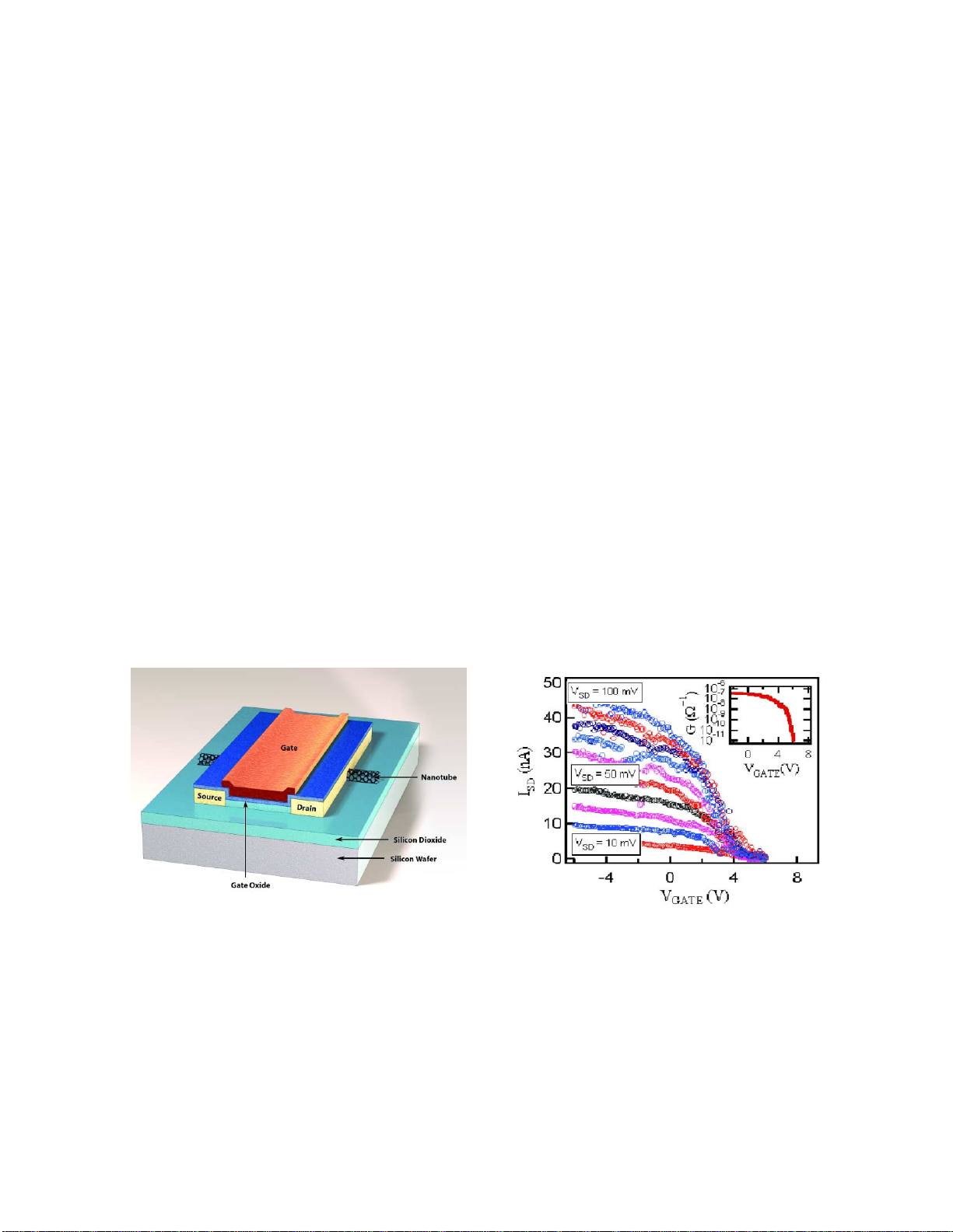
The CNT FET uses a nanotube that is laid across two gold contacts that serve as the
source and drain, as shown in Figure 1a. The nanotube essentially becomes the current
carrying channel for the FET. DC characterization of this type of device is carried out just as
with any other FET. An example is shown in Figure 1b.
A Greater Measure of Confidence
Figure 1b shows that the amount of current (ISD) flowing through a nanotube channel
can be changed by varying the voltage applied to the gate (VG) [2]. Other tests typically
performed on such devices include a transconductance curve (upper right corner of Figure
Figure 1a. Schematic cross-section of IBM’s CNFET (carbon
nanotube field effect transistor) [2] IBM Copyright.
Figure 1b. ISDversus VGfor an IBM nanotube FET [2]. The
different color plots represent different source-drain
voltages. IBM Copyright
Page 3
1b), gate leakage, leakage current vs. temperature, substrate to drain leakage, and subthreshold current. Since these types of devices are still in the research stage, measurements
that provide insight into fundamental properties of conduction, such as transport mechanisms
and I-V vs. temperature, are critical.
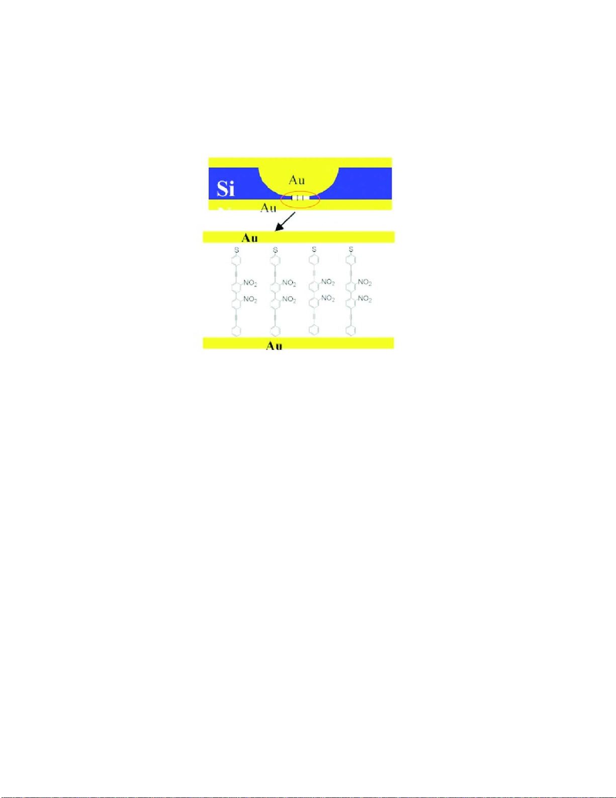
Figure 2. Nanopore structure [3]. Graphic courtesy of Mark A. Reed Research Group,Yale University.
Polyphenylene molecules are another approach to developing active electronic
components. The nanopore test structure shown in Figure 2 is based on polyphenylene
molecules deposited between two gold electrodes on a silicon wafer. This structure serves as
a probe pad, allowing a researcher to make probe connections for I-V characterization of
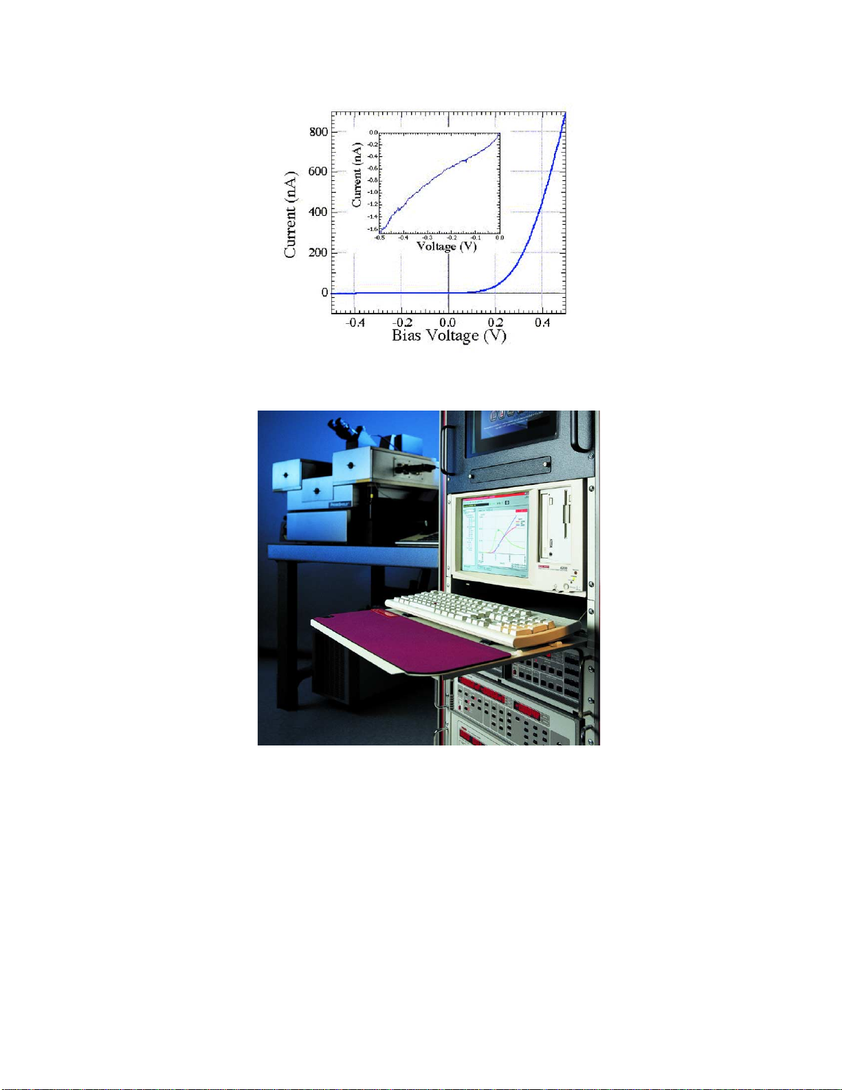
nanoscale devices, such as molecular diodes (see Figure 3).
With such I-V curves, researchers have determined that molecules can conduct small
amounts of electrical current. Although I-V measurement methods are typical for device
characterization, the levels of current measured are lower than those of many semiconductor
devices fabricated today.
I-V characterization of moletronic devices requires low level current measurements in
the nanoamp to femtoamp range. To complicate matters, these measurements are quite often
made at cryogenic temperatures. Therefore, highly sensitive instruments are required, and
appropriate measurement and connection techniques must be employed to avoid errors.
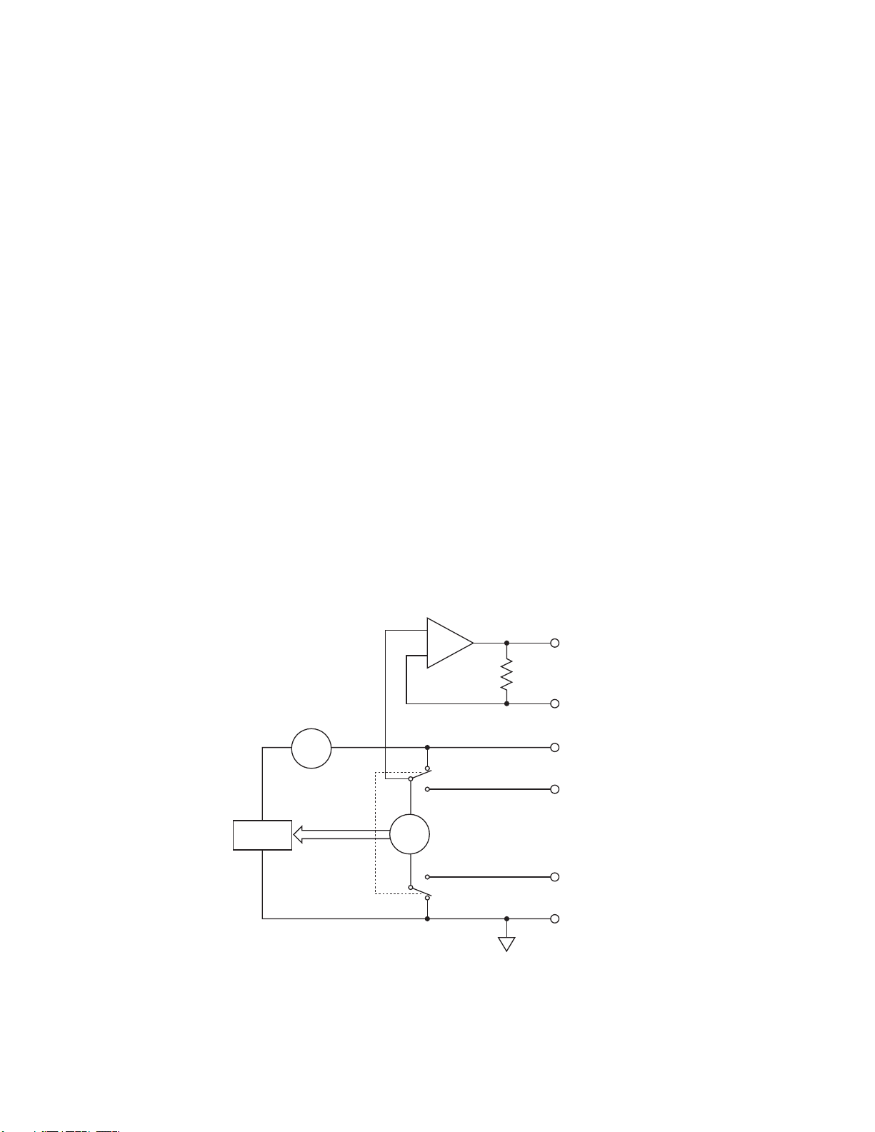
Typically, nanoelectronic and moletronic devices are characterized with semiconductor test
instruments and probe station systems, such as the one shown in Figure 4.
A Greater Measure of Confidence
Page 4
Minimizing Sources of Measurement Error
As good as semiconductor characterization systems are, making ultra-low current
measurements on nanoelectronic and moletronic devices is not trivial. Potential sources of
measurement error must be understood and steps taken to reduce or eliminate them.
Otherwise, a researcher will lack confidence in the characterization of materials and devices
under test (DUTs). The following examples and techniques can improve low level current
measurements.
A Greater Measure of Confidence
Figure 3. I-V curve for a molecular diode at room temperature [3]. Graphic courtesy of Mark A. Reed Research Group,Yale University.
Figure 4. Example of a Windows®-based semiconductor characterization system, the Keithley Model 4200-SCS.
Page 5
A Greater Measure of Confidence
Leakage Currents and Guarding. Low currents in the nanoamp to picoamp range must
often be measured in nanoelectronic devices, so external leakage current error sources must
be minimized, and instrument system leakage quantified. External leakage currents typically
are generated between the measurement circuit and nearby voltage sources. These currents
significantly degrade the accuracy of low current measurements. Techniques for minimizing
leakage currents in a test circuit include the use of high quality insulators (Teflon,
polyethylene, and sapphire), reducing the humidity of the test environment, and guarding.
Insulators absorb water vapor from the air, with the amount absorbed dependant on
insulator material and humidity level. When the insulator contains ionic contaminants,
spurious current generation can be especially troublesome in high humidity environments.
The best insulator choice is one on which water vapor does not readily form a continuous
film. However, this may be unavoidable if the DUT absorbs water easily. In that case, it’s best
to make the measurements in an environmentally controlled, low humidity room.
The use of guarding is a principal method of reducing leakage currents in a test
circuit. Aguard is a conductor connected to a low impedance point in the circuit that is at
nearly the same potential as the high impedance lead being guarded (for example, In/Out Hi
in Figure 5). Guarding can isolate the high impedance input lead of an electrometer,
picoammeter, or source-measure unit (SMU) from leakage current due to voltage sources.
Guarding can also reduce the effect of shunt capacitance in the measurement circuit.
Figure 5. Simplified block diagram of a source-measure unit (SMU) configured to source voltage and measure current,
showing guard connections.
V Source
I Meter
Sense
Output
V Source
(Feedback)
+
x1
–
Local
Remote
V Meter
Adjust
Remote
Local
Guard
Guard Sense
In/Out HI
Sense HI
Sense LO
In/Out LO
Page 6
Grounding and Shielding. It is important to distinguish between an instrument’s
common and chassis grounds. These two grounds are different. The common is the ground
for the complete measurement circuit; it will affect the system’s low level measurement
performance. In contrast, the chassis ground is connected to the power line ground and is
mainly used for safety reasons. Usually, there are no problems associated with connecting
these grounds together. Sometimes, however, the power line ground can be noisy. In other
cases, a test fixture and probe station connected to the instrument may create a ground loop
that generates additional noise. Accurate low level measurements require a comprehensive
system grounding plan.
Although grounding and shielding are closely related, they are actually two different
issues. In a test fixture or probe station, the DUT and probe typically are enclosed in soft
metal shielding. The metal enclosure helps eliminate interference from power lines and high
frequency radiation (RF or microwave), and reduces magnetic interference. The metal
normally is grounded for safety reasons.
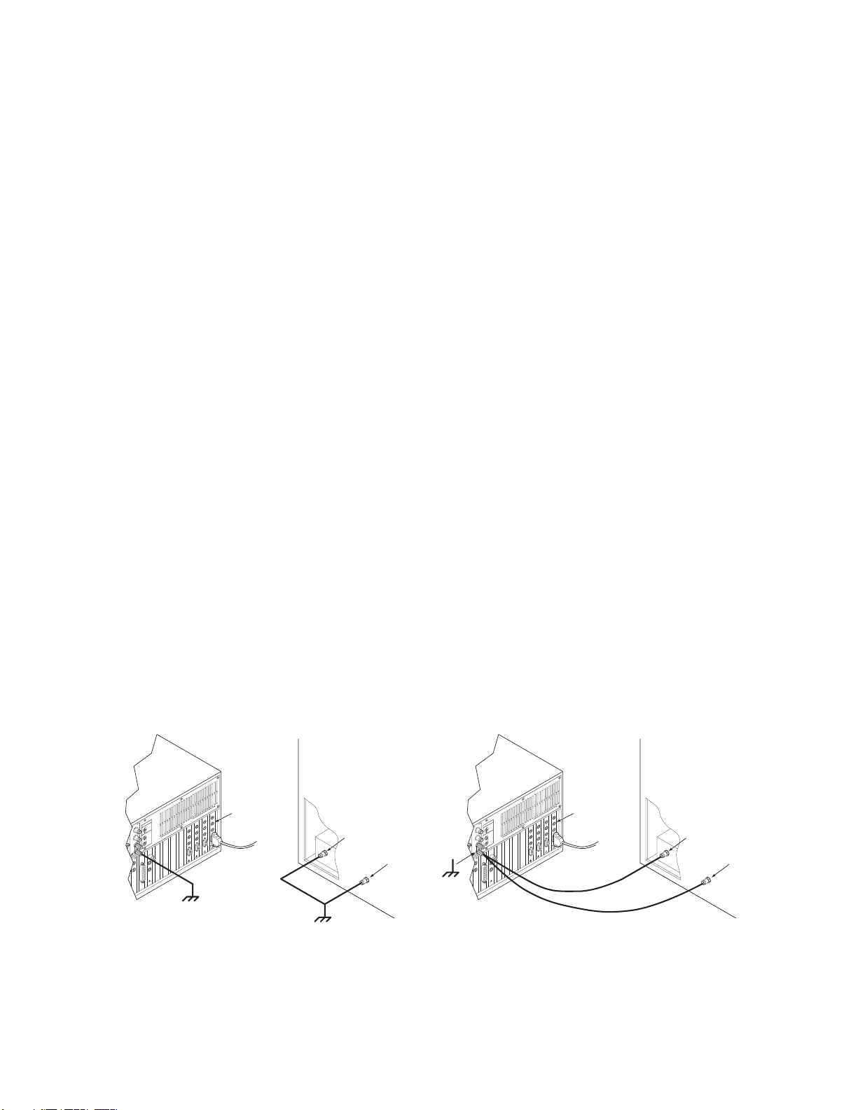
However, when an instrument is connected to a probe station through triaxial cables
(the type used for guarded connections), physical grounding points are very important. The
configuration in Figure 6a illustrates a common grounding error. Note that the instrument
common and the chassis ground are connected. The probe station is also grounded to the
power line locally. Even more significant, the measurement instrument and the probe station
are connected to different power outlets. The power line grounds of these two outlets may not
be at the same electrical potential all the time. Therefore, a fluctuating current may flow
between the instrument and the probe station. This creates what is known as a ground loop.
To avoid ground loops, a single point ground must be used. Figure 6b illustrates a better
grounding scheme for use with a probe station.
A Greater Measure of Confidence
Figure 6a. Grounding connections that create ground loops.
Figure 6b. Grounding connections that avoid ground loops.
T
O
L
S
1
T
O
L
SMU
S
2
O
L
E
S
N
E
T
S
O
L
S
3
O
L
E
S
S
E
N
T
S
E
N
N
T
S
E
E
O
S
M
L
S
U
R
4
T
S
O
L
N
I
E
S
E
N
S
E
T
N
S
E
O
S
L
S
E
C
5
R
O
O
F
L
E
S
E
N
S
E
T
N
S
E
O
S
L
S
E
C
6
R
O
F
E
S
N
E
S
E
C
R
O
F
E
C
R
O
F
L
R
T
N
C
A
P
L
R
T
N
C
A
P
L
R
T
N
C
A
P
Prober
GND
Probe
Station
“Dark Box”
GND
T
N
E
S
N
M
O
U
I
R
T
T
C
S
Y
O
E
L
L
U
N
N
I
N
D
E
N
S
D
O
N
O
N
R
G
E
A
U
C
S
U
M
O
G
L
S
E
S
N
E
S
N
O
M
M
S
O
U
C
D
E
N
G
N
D
S
N
A
E
U
E
S
M
N
S
E
S
N
O
M
F
M
O
C
O
R
D
R
E
A
C
C
U
R
G
O
E
F
C
O
M
M
O
N
K
L
T
N
I
N
I
T
U
O
Model 4200-SCS
Mainframe
T
O
L
S
1
T
O
L
SMU
S
2
O
L
E
S
N
E
T
S
O
L
S
3
O
L
E
S
S
E
N
T
S
E
N
N
T
S
E
E
O
S
M
L
S
U
R
4
T
S
O
L
N
I
E
S
E
N
S
E
T
N
S
E
O
S
L
S
E
C
5
R
O
O
F
L
E
S
E
N
S
E
T
N
S
E
O
S
L
S
E
C
6
R
O
F
E
S
T
N
O
E
L
S
S
E
7
C
R
O
F
T
O
L
S
E
8
C
R
O
F
L
R
T
N
C
A
P
L
R
T
N
C
A
P
L
R
T
N
C
A
P
Prober
GND
Probe
Station
“Dark Box”
GND
T
N
E
S
N
M
O
U
I
R
T
T
C
S
Y
O
E
L
L
U
N
N
I
N
D
E
N
S
D
O
N
O
N
R
G
E
A
U
C
S
U
M
O
G
L
S
E
S
N
E
S
N
O
M
M
S
O
U
C
D
E
N
G
N
D
S
N
A
E
U
E
S
M
N
S
E
S
N
O
M
F
M
O
C
O
R
D
R
E
A
C
C
U
R
G
O
E
F
C
O
M
M
O
N
K
L
T
N
I
N
I
T
U
O
Model 4200-SCS
Mainframe
T
O
L
S
7
T
O
L
S
8
Page 7

Minimizing System and Instrument Noise. Even if a characterization system is
properly shielded and grounded, it’s still possible for noise to corrupt measurement results.
Typically, instruments contribute very little to the total noise error in the measurements. For
example, a good characterization system has a noise specification of about 0.2% of range,
meaning the p-p noise on the lowest current range is just a few femtoamps. Noise can be
further reduced with proper signal averaging (through filtering and/or increasing the
measurement integration period, i.e., integrating over a larger number of power line cycles).
The most likely sources of noise are other test system components, such as long
cables or switching hardware inappropriate for the application. Therefore, it is advisable to
use the best switch matrix available, designed specifically for ultra-low current
measurements. Then, keep all connecting cables as short as possible.
Generally, system noise has the greatest impact on measurement integrity when the
DUT signal is very small (i.e., low signal-to-noise ratio). This leads to the classic problem of
amplifying noise along with the signal. Clearly then, increasing the signal-to-noise ratio is
key to low level measurement accuracy.
Some characterization systems offer a low noise pre-amplifier option that allows
measurements down to the sub-femptoamp level. To get that level of sensitivity, it is best to
mount the pre-amps remotely on a probe station platen. With this arrangement, the signal
must travel only a very short distance (just the length of the probe needle) before it is
amplified. Then, the amplified signal is routed through the cables and switch matrix into the
measurement hardware.
Test System Settling Time. Fast, accurate low current measurements depend a great
deal on the way system elements work together. Measuring instruments must be properly
synchronized with the prober and switching matrix, if one is used. Improper synchronization
and source-measure delay may lead to collection of signals unrelated to the real device
parameters.
A step voltage test is typically used to characterize system settling time. A 10V step is
applied across two open-circuit probe tips, and then current is monitored continuously for a
period of time. The resulting current vs. time (I-t) curve (Figure 7) reveals several important
system characteristics.
A Greater Measure of Confidence
Page 8
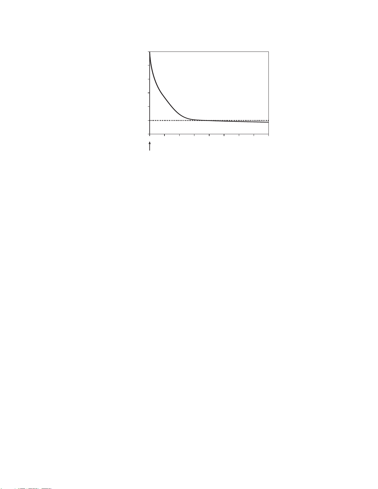
Figure 7. Use instrument settling time to set source-measure delays. Leakage current (in this case, 10
–15
A) establishes the limit on
basic instrument sensitivity.
There are two regions of interest on the I-t curve: the transient segment and the steady
current segment. Immediately after the voltage step, the transient current will gradually decay
to a steady value. The time it takes to reach the steady value is the system settling time.
Typically, the time needed to reach 1/e of the initial value is defined as the system time
constant.
Settling time can vary widely for different systems, equipment, and cabling. It results
mainly from capacitance inherent in switch relays, cables, etc., but may also be affected by
dielectric absorption in the insulating materials of system components. High dielectric
absorption can cause settling time to be quite long.
In most test situations, it is desirable to shorten test time to the minimum required for
acceptable accuracy. This requires using the optimum source-measure delay, which is a
function of the instrumentation source and measurement time, along with the system settling
time. The latter usually is the dominant portion of source-measure delay time.
With the system leakage I-t curve in hand, the next step is to establish the acceptable
measurement sensitivity or error. Suppose the task requires accurate DUT leakage
measurements only at the picoamp level. Then, source-measure delay time can be established
by a point on the transient portion of the system settling curve (Figure 7) where the leakage
current is at a sub-picoamp level. If the expected DUT current is in the femtoamp range, then
the delay time must be extended so that the transient current reaches a value lower than the
expected reading before a measurement is taken.
1e–10
A Greater Measure of Confidence
1e–11
1e–12
Current
(Amps)
1e–13
1e–14
1e–15
1e–16
0.0 0.5 1.0 1.5 2.0 2.5 3.0 3.5 4.0
Time (seconds)
Step voltage
applied
Page 9
Sources of Current Errors
System leakage current. Once the transient current has settled to its steady value, it
corresponds to the system leakage current. Typically, system leakage current is expressed as
amperes per volt. To determine its magnitude, simply measure the steady-state current and
divide by the voltage step value. The magnitude of the system leakage current establishes the
noise floor and overall sensitivity of the system. Usually, the largest leakage current
contributors are the probe card and switching relays.
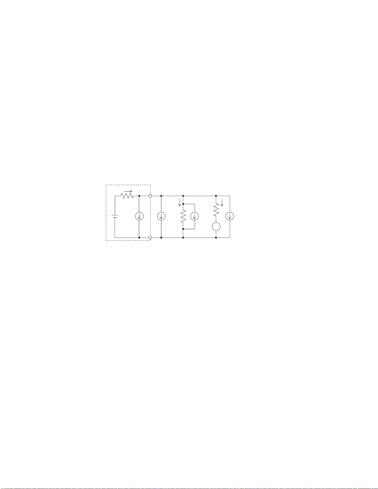
General error current model. Errors in current measuring instruments arise from
extraneous currents flowing through various circuit elements. In the current measurement
model of Figure 8, the current indicated on the meter (M) is equal to the actual current
through the meter (I
1
), plus or minus inherent meter uncertainty. I1is the signal current (IS),
less the shunt current (ISH) and the sum of all generated error currents (IE).
Figure 8. Sources of current error in a shunt type ammeter.
Figure 8 identifies the various noise and error currents generated during typical
current measurements, which contribute to the error sum (IE). The ISEcurrent generator
represents noise currents produced within the DUT and its voltage source. These currents
could arise due to the aforementioned leakage and dielectric absorption, or due to
electrochemical, piezoelectric, and triboelectric effects. ICErepresents currents generated in
the interconnection between the meter and the source/DUT circuit. IIErepresents the error
current arising from all internal measuring instrument sources. IREis generated by the thermal
activity of the shunt resistance. The rms value of this thermal noise current is given by:
IRE= (4kTf/RSH)
1/2
where: k = Boltzman’s constant (1.38 × 10
–23
J/K)
T= absolute temperature in °K
f = noise bandwidth in Hz
RSH= resistance in ohms
A Greater Measure of Confidence
I
S
I1= IS – ISH – I
VISEI
SE
Current Source
I
=
Source current
S
=
Source noise current
I
SE
=
Interconnection noise current
I
CE
I
CE
IE= ISE + ICE + IRE + I
I
1
R
SH
IE
I
RE
R
=
Shunt resistance
SH
=
Shunt resistance noise
I
RE
=
Instrument error current
I
IE
I
IE
M
E
Page 10

Making the Most of Instrumentation
Making accurate low current measurements on nanoelectronic and moletronic devices
demands a thorough analysis of potential error sources, plus steps to reduce possible errors.
These steps include selection of appropriate grounding and shielding techniques, cables,
probe cards, switching matrices, etc. These efforts allow nanotechnology researchers to make
the most of the capabilities inherent in modern device characterization systems.
Properly applied, these systems can speed up development of CNT and molecular
electronic structures, which may ultimately redefine the processes used to fabricate
semiconductor devices. By providing a means for economical, massive integration, such
technology could pave the way for new computing architectures, 100× speed increases,
significant reduction in power consumption, and other breakthroughs in performance.
Page 11

Works Consulted
[1] Yi Cui, Charles Lieber, “Functional Nanoscale Electronic Devices Assembled Using
Silicon Building Blocks,” Science, vol. 291, pp. 851-853, Jan. 2, 2002.
[2] Nanoscale Science Department. (2001, October 1). Nanotube field-effect transistor. IBM
T. J. Watson Research Center, Yorktown Heights, NY. [Online]. Available:
http://www.research.ibm.com/nanoscience/fet.html
[3] Mark A. Reed Research Group. (2002, April 18). Molecular Electronic Devices. Yale
University. New Haven, CT. Available at:
http://www.eng.yale.edu/reedlab/research/device/mol_devices.html
Acknowledgements
The author extends his sincere appreciation to Dr. James Tour of Rice University, Dr.
Mark Reed of Yale University, and Dr. Curt Richter of NIST for their thoughtful peer reviews
and other contributions to this article.
About the Author
Jonathan Tucker is a Lead Industry Consultant at Keithley Instruments in Cleveland,
Ohio, where he is responsible for new application test and measurement development in the
Research and Education market segments. He received his Bachelor of Electrical Engineering
degree from Cleveland State University and an MBA from Kent State University, and has 18
years of experience in test and measurement.
A Greater Measure of Confidence
Page 12

Specifications are subject to change without notice.
All Keithley trademarks and trade names are the property of Keithley Instruments, Inc. All other
trademarks and trade names are the property of their respective companies.
Keithley Instruments, Inc. 28775 Aurora Road • Cleveland, Ohio 44139 • 440-248-0400 • Fax: 440-248-6168
1-888-KEITHLEY (534-8453) • www.keithley.com
© Copyright 2002 Keithley Instruments, Inc. No. 2421
Printed in the U.S.A. 11022KGW
 Loading...