

Page 1

KUSB-3160
User’s Manual
KUSB3160-900-01 Rev. A / January 2005
www.keithley.com
A GR
EATER MEASURE OF CONFIDENCE
Page 2

WARRANTY
Keithley Instruments, Inc. warrants this product to be free from defects in material and workmanship for a period of 3 years from
date of shipment.
Keithley Instruments, Inc. warrants the following items for 90 days from the date of shipment: probes, cables, rechargeable batteries,
diskettes, and documentation.
During the warranty period, we will, at our option, either repair or replace any product that proves to be defective.
To exercise this warranty, write or call your local Keithley representative, or contact Keithley headquarters in Cleveland, Ohio.
You will be given prompt assistance and return instructions. Send the product, transportation prepaid, to the indicated service facility. Repairs will be made and the product returned, transportation prepaid. Repaired or replaced products are warranted for the balance of the original warranty period, or at least 90 days.
LIMITATION OF WARRANTY
This warranty does not apply to defects resulting from product modification without Keithley’s express written consent, or misuse
of any product or part. This warranty also does not apply to fuses, software, non-rechargeable batteries, damage from battery leakage, or problems arising from normal wear or failure to follow instructions.
THIS WARRANTY IS IN LIEU OF ALL OTHER WARRANTIES, EXPRESSED OR IMPLIED, INCLUDING ANY IMPLIED
WARRANTY OF MERCHANTABILITY OR FITNESS FOR A PARTICULAR USE. THE REMEDIES PROVIDED HEREIN
ARE BUYER’S SOLE AND EXCLUSIVE REMEDIES.
NEITHER KEITHLEY INSTRUMENTS, INC. NOR ANY OF ITS EMPLOYEES SHALL BE LIABLE FOR ANY DIRECT,
INDIRECT, SPECIAL, INCIDENTAL OR CONSEQUENTIAL DAMAGES ARISING OUT OF THE USE OF ITS INSTRUMENTS AND SOFTWARE EVEN IF KEITHLEY INSTRUMENTS, INC., HAS BEEN ADVISED IN ADVANCE OF THE
POSSIBILITY OF SUCH DAMAGES. SUCH EXCLUDED DAMAGES SHALL INCLUDE, BUT ARE NOT LIMITED TO:
COSTS OF REMOVAL AND INSTALLATION, LOSSES SUSTAINED AS THE RESULT OF INJURY TO ANY PERSON,
OR DAMAGE TO PROPERTY.
A G R E A T E R M E A S U R E O F C O N F I D E N C E
Keithley Instruments, Inc.
Corporate Headquarters • 28775 Aurora Road • Cleveland, Ohio 44139
440-248-0400 • Fax: 440-248-6168 • 1-888-KEITHLEY (534-8453) • www.keithley.com
12/04
Page 3

KUSB-3160
User’s Manual
©2005, Keithley Instruments, Inc.
All rights reserved.
First Printing, January 2005
Cleveland, Ohio, U.S.A.
Document Number: KUSB3160-900-01A Rev. A
Page 4

Manual Print History
The print history shown below lists the printing dates of all Revisions and Addenda created for this manual. The Revision Level letter increases alphabetically as the manual undergoes subsequent updates. Addenda, which are released
between Revisions, contain important change information that the user should incorporate immediately into the manual.
Addenda are numbered sequentially. When a new Revision is created, all Addenda associated with the previous Revision
of the manual are incorporated into the new Revision of the manual. Each new Revision includes a revised copy of this
print history page.
Revision A (Document Number KUSB3160-900-01A) ...................................................................... January 2005
All Keithley product names are trademarks or registered trademarks of Keithley Instruments, Inc.
Other brand and product names are trademarks or registered trademarks of their respective holders.
Page 5

Safety Precautions
The following safety precautions should be observed before using
this product and any associated instrumentation. Although some instruments and accessories would normally be used with non-hazardous voltages, there are situations where hazardous conditions
may be present.
This product is intended for use by qualified personnel who recognize shock hazards and are familiar with the safety precautions required to avoid possible injury. Read and follow all installation,
operation, and maintenance information carefully before using the
product. Refer to the manual for complete product specifications.
If the product is used in a manner not specified, the protection provided by the product may be impaired.
The types of product users are:
Responsible body is the individual or group responsible for the use
and maintenance of equipment, for ensuring that the equipment is
operated within its specifications and operating limits, and for ensuring that operators are adequately trained.
Operators use the product for its intended function. They must be
trained in electrical safety procedures and proper use of the instrument. They must be protected from electric shock and contact with
hazardous live circuits.
Maintenance personnel perform routine procedures on the product to keep it operating properly, for example, setting the line voltage or replacing consumable materials. Maintenance procedures
are described in the manual. The procedures explicitly state if the
operator may perform them. Otherwise, they should be performed
only by service personnel.
Service personnel are trained to work on live circuits, and perform
safe installations and repairs of products. Only properly trained service personnel may perform installation and service procedures.
Keithley products are designed for use with electrical signals that
are rated Measurement Category I and Measurement Category II, as
described in the International Electrotechnical Commission (IEC)
Standard IEC 60664. Most measurement, control, and data I/O signals are Measurement Category I and must not be directly connected to mains voltage or to voltage sources with high transient overvoltages. Measurement Category II connections require protection
for high transient over-voltages often associated with local AC
mains connections. Assume all measurement, control, and data I/O
connections are for connection to Category I sources unless otherwise marked or described in the Manual.
Exercise extreme caution when a shock hazard is present. Lethal
voltage may be present on cable connector jacks or test fixtures.
The American National Standards Institute (ANSI) states that a
shock hazard exists when voltage levels greater than 30V RMS,
42.4V peak, or 60VDC are present. A good safety practice is to ex-
pect that hazardous voltage is present in any unknown circuit
before measuring.
Operators of this product must be protected from electric shock at
all times. The responsible body must ensure that operators are prevented access and/or insulated from every connection point. In
some cases, connections must be exposed to potential human contact. Product operators in these circumstances must be trained to
protect themselves from the risk of electric shock. If the circuit is
capable of operating at or above 1000 volts, no conductive part of
the circuit may be exposed.
Do not connect switching cards directly to unlimited power circuits.
They are intended to be used with impedance limited sources.
NEVER connect switching cards directly to AC mains. When connecting sources to switching cards, install protective devices to limit
fault current and voltage to the card.
Before operating an instrument, make sure the line cord is connected to a properly grounded power receptacle. Inspect the connecting
cables, test leads, and jumpers for possible wear, cracks, or breaks
before each use.
When installing equipment where access to the main power cord is
restricted, such as rack mounting, a separate main input power disconnect device must be provided, in close proximity to the equipment and within easy reach of the operator.
For maximum safety, do not touch the product, test cables, or any
other instruments while power is applied to the circuit under test.
ALWAYS remove power from the entire test system and discharge
any capacitors before: connecting or disconnecting cables or jumpers, installing or removing switching cards, or making internal
changes, such as installing or removing jumpers.
Do not touch any object that could provide a current path to the common side of the circuit under test or power line (earth) ground. Always
make measurements with dry hands while standing on a dry, insulated
surface capable of withstanding the voltage being measured.
The instrument and accessories must be used in accordance with its
specifications and operating instructions or the safety of the equipment may be impaired.
Do not exceed the maximum signal levels of the instruments and accessories, as defined in the specifications and operating information, and as shown on the instrument or test fixture panels, or
switching card.
When fuses are used in a product, replace with same type and rating
for continued protection against fire hazard.
Chassis connections must only be used as shield connections for
measuring circuits, NOT as safety earth ground connections.
If you are using a test fixture, keep the lid closed while power is applied to the device under test. Safe operation requires the use of a
lid interlock.
5/03
Page 6

If a screw is present, connect it to safety earth ground using the
wire recommended in the user documentation.
!
The symbol on an instrument indicates that the user should refer to the operating instructions located in the manual.
The symbol on an instrument shows that it can source or measure 1000 volts or more, including the combined effect of normal
and common mode voltages. Use standard safety precautions to
avoid personal contact with these voltages.
The symbol indicates a connection terminal to the equipment
frame.
The WARNING heading in a manual explains dangers that might
result in personal injury or death. Always read the associated information very carefully before performing the indicated procedure.
The CAUTION heading in a manual explains hazards that could
damage the instrument. Such damage may invalidate the warranty.
Instrumentation and accessories shall not be connected to humans.
Before performing any maintenance, disconnect the line cord and
all test cables.
To maintain protection from electric shock and fire, replacement
components in mains circuits, including the power transformer, test
leads, and input jacks, must be purchased from Keithley Instruments. Standard fuses, with applicable national safety approvals,
may be used if the rating and type are the same. Other components
that are not safety related may be purchased from other suppliers as
long as they are equivalent to the original component. (Note that selected parts should be purchased only through Keithley Instruments
to maintain accuracy and functionality of the product.) If you are
unsure about the applicability of a replacement component, call a
Keithley Instruments office for information.
To clean an instrument, use a damp cloth or mild, water based
cleaner. Clean the exterior of the instrument only. Do not apply
cleaner directly to the instrument or allow liquids to enter or spill on
the instrument. Products that consist of a circuit board with no case
or chassis (e.g., data acquisition board for installation into a computer) should never require cleaning if handled according to instructions. If the board becomes contaminated and operation is affected,
the board should be returned to the factory for proper cleaning/servicing.
Page 7

Table of Contents
About this Manual . . . . . . . . . . . . . . . . . . . . . . . . . . . . . . . . . . ix
Intended Audience. . . . . . . . . . . . . . . . . . . . . . . . . . . . . . . . . . . . . . ix
What You Should Learn from this Manual. . . . . . . . . . . . . . . . . . ix
Conventions Used in this Manual . . . . . . . . . . . . . . . . . . . . . . . . . . x
Related Information . . . . . . . . . . . . . . . . . . . . . . . . . . . . . . . . . . . . . . x
Where To Get Help. . . . . . . . . . . . . . . . . . . . . . . . . . . . . . . . . . . . . . xi
Chapter 1: Overview . . . . . . . . . . . . . . . . . . . . . . . . . . . . . . . . 1
Key Features . . . . . . . . . . . . . . . . . . . . . . . . . . . . . . . . . . . . . . . . . . . . 2
Supported Software . . . . . . . . . . . . . . . . . . . . . . . . . . . . . . . . . . . . . . 3
Accessories . . . . . . . . . . . . . . . . . . . . . . . . . . . . . . . . . . . . . . . . . . . . . 4
Chapter 2: Principles of Operation . . . . . . . . . . . . . . . . . . . . 5
Digital I/O Lines . . . . . . . . . . . . . . . . . . . . . . . . . . . . . . . . . . . . . . . . 8
Resolution . . . . . . . . . . . . . . . . . . . . . . . . . . . . . . . . . . . . . . . . . . . . . 10
Interrupts. . . . . . . . . . . . . . . . . . . . . . . . . . . . . . . . . . . . . . . . . . . . . . 13
Operation Modes . . . . . . . . . . . . . . . . . . . . . . . . . . . . . . . . . . . . . . . 14
Chapter 3: Supported Device Driver Capabilities. . . . . . . . 15
Chapter 4: Programming Flowcharts. . . . . . . . . . . . . . . . . . 25
Single-Value Operations . . . . . . . . . . . . . . . . . . . . . . . . . . . . . . . . . 27
Continuous Digital Input Operations . . . . . . . . . . . . . . . . . . . . . . 29
Chapter 5: Troubleshooting . . . . . . . . . . . . . . . . . . . . . . . . . 33
General Checklist . . . . . . . . . . . . . . . . . . . . . . . . . . . . . . . . . . . . . . . 34
Service and Support. . . . . . . . . . . . . . . . . . . . . . . . . . . . . . . . . . . . . 37
vii
Page 8

Contents
Appendix A: Specifications . . . . . . . . . . . . . . . . . . . . . . . . . 39
Appendix B: Connector Pin Assignments . . . . . . . . . . . . . 43
Index . . . . . . . . . . . . . . . . . . . . . . . . . . . . . . . . . . . . . . . . . . . . . 53
viii
Page 9

About this Manual
This manual describes the features of the KUSB-3160 module, the
capabilities of the device driver, and how to program the KUSB-3160
module using DT-Open Layers™ software. Troubleshooting
information is also provided.
Intended Audience
This document is intended for engineers, scientists, technicians, or
others responsible for using and/or programming the KUSB-3160
module for data acquisition operations in the Microsoft® Windows
2000 or Windows XP operating systems. It is assumed that you have
some familiarity with data acquisition principles and that you
understand your application.
What You Should Learn from this Manual
This manual provides detailed information about the features of the
KUSB-3160 module and the capabilities of the device driver. It is
organized as follows:
• Chapter 1, “Overview,” describes the major features of the
modules, as well as the supported software and accessories for
the modules.
• Chapter 2, “Principles of Operation,” describes all of the features
of the modules and how to use them in your application.
• Chapter 3, “Supported Device Driver Capabilities,” lists the data
acquisition subsystems and the associated features accessible
using the device driver.
• Chapter 4, “Programming Flowcharts,” describes the processes
you must follow to program the subsystems on the KUSB-3160
module using DT-Open Layers-compliant software.
ix
Page 10

About this Manual
Conventions Used in this Manual
• Chapter 5, “Troubleshooting,” provides information that you can
use to resolve problems with the modules and the device driver,
should they occur.
• Appendix A, “Specifications,” lists the specifications of the
module.
• Appendix B, “Connector Pin Assignments,” shows the pin
assignments for the connectors and the screw terminal
assignments for the module.
• An index completes this manual.
The following conventions are used in this manual:
• Notes provide useful information or information that requires
special emphasis, cautions provide information to help you avoid
losing data or damaging your equipment, and warnings provide
information to help you avoid catastrophic damage to yourself or
your equipment.
• Items that you select or type are shown in bold.
Related Information
Refer to the following documents for more information on using the
KUSB-3160 module:
• KUSB-3160 Getting Started Manual. This manual describes the
how to install the KUSB-3160 module and related software.
• DataAcq SDK User’s Manual. For programmers who are
developing their own application programs using the Microsoft
C compiler, this manual describes how to use the DT-Open
TM
Layers
access the capabilities of your module.
x
DataAcq SDKTM in Windows 2000 or Windows XP to
Page 11

• DTx-EZ Getting Started Manual. This manual describes how to use
the ActiveX controls provided in DTx-EZ
capabilities of your module in Microsoft Visual Basic® or Visual
C++®.
• DT-LV Link Getting Started Manual. This manual describes how to
use DT-LV Link
language to access the capabilities of your module.
• Microsoft Windows 2000 or Windows XP documentation.
• USB web site (http://www.usb.org).
Where To Get Help
Should you run into problems installing or using your KUSB-3160
module, please call the Keithley Technical Support Department.
About this Manual
TM
to access the
TM
with the LabVIEW® graphical programming
xi
Page 12

About this Manual
xii
Page 13

1
Overview
Key Features . . . . . . . . . . . . . . . . . . . . . . . . . . . . . . . . . . . . . . . . . . . . 2
Supported Software . . . . . . . . . . . . . . . . . . . . . . . . . . . . . . . . . . . . . . 3
Accessories . . . . . . . . . . . . . . . . . . . . . . . . . . . . . . . . . . . . . . . . . . . . . 4
1
Page 14

Chapter 1
Key Features
The KUSB-3160 is a low-cost, high-power, digital I/O module for the
Universal Serial Bus (USB). The KUSB-3160 module provides the
following major features:
• USB compatibility;
• 64 configurable digital I/O lines (configurable in banks of eight)
and 32 dedicated digital input lines for nonclocked monitoring or
control.
• Interrupt-on-change on 16 dedicated digital input lines.
• External solid-state relay module support. Digital outputs can
drive sink 12 mA, source 100 kΩ pullup.
• Isolated output common from the USB bus to 500 V peak.
2
Page 15

Supported Software
The following software is available for use with the KUSB-3160
module:
• Device Driver − This software is provided on the CD shipped
with the module. The device driver allows you to use a
KUSB-3160 module with any of the supported software packages
or utilities. Refer to the KUSB-3160 Getting Started Manual for
more information on loading and configuring the device driver.
• Quick Data Acq application − This application provides a quick
way to get a KUSB-3160 module up and running. Using the
Quick Data Acq application, you can verify the features of the
module, display data on the screen, and save data to disk.
• DataAcq SDK − This DT-Open Layers Software Develop Kit
(SDK) allows programmers to develop application programs for
the KUSB-3160 using the Microsoft C compiler in Windows 2000
or Windows XP.
• DTx-EZ − This software package contains ActiveX controls that
allow Microsoft Visual Basic® or Visual C++® programmers to
access the capabilities of the KUSB-3160 module.
• DT-LV Link − This software package allows LabVIEW®
programmers to access the capabilities of the KUSB-3160 module.
Overview
1
1
1
1
1
1
1
1
1
3
Page 16

Chapter 1
Accessories
The following accessories are provided for the KUSB-3160 module:
• KUSB-STP100 − a 100 mm x 160 mm screw terminal panel that
connects to the KUSB-3160 module using the KUSB-CABDIO
cable. This screw terminal panel allows you to connect all of the
input and output connections that are supported by a KUSB-3160
module. LEDs on up to 64 of the outputs light when the outputs
are low. Note that the LEDs are not provided for the dedicated
digital input lines.
• KUSB-CABDIO − a 1-meter, 100-conductor cable that connects
the KUSB-STP100 screw terminal panel to the KUSB-3160
module.
4
Page 17

2
Principles of Operation
Digital I/O Lines . . . . . . . . . . . . . . . . . . . . . . . . . . . . . . . . . . . . . . . . 8
Resolution . . . . . . . . . . . . . . . . . . . . . . . . . . . . . . . . . . . . . . . . . . . . . 10
Interrupts. . . . . . . . . . . . . . . . . . . . . . . . . . . . . . . . . . . . . . . . . . . . . . 13
Operation Modes . . . . . . . . . . . . . . . . . . . . . . . . . . . . . . . . . . . . . . . 14
5
Page 18
Chapter 2
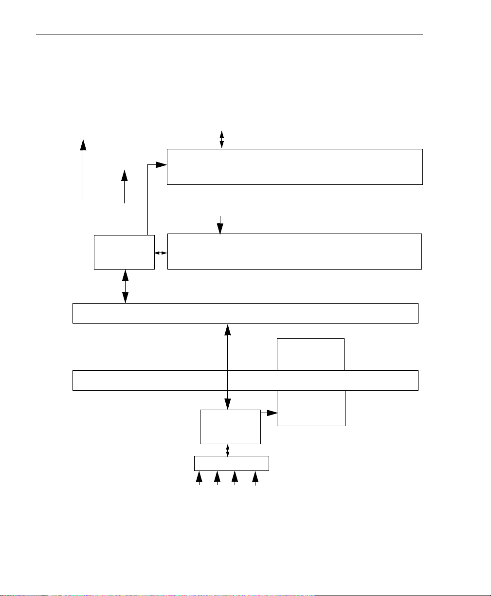
Pins 50 and 100
Figure 1 shows a block diagram of the KUSB-3160 module. Note that
bold entries indicate signals you can access.
Pins 1 to 64
Lines 0 to 63
Pins 49 and 99
Isolated
Common
+5 V
In/Out
Controller and
Digital Filters
Pins 64 to 96
Lines 63 to 95
High-Speed
Isolated Data Path
Microcontroller
64 Digital I/O WIth 100 kΩ Pull-Ups to +5V_I
WIth Back EMF Protection
32 Digital Inputs WIth 100 kΩ Pull-Ups to +5V_I
WIth Back EMF Protection
Isolated Power
500 V Isolation Barrier
Power Control
DC to DC
USB Interface
+5 V D + D - GND
Figure 1: Block Diagram of the KUSB-3160 Module
6
Page 19

Principles of Operation
This chapter describes the following features of the digital I/O
subsystem:
• Digital I/O lines, described on page 8;
• Resolution, described on page 10;
2
• Interrupts, described on page 13, and
• Operation modes, described on page 14.
2
2
2
2
2
2
2
2
7
Page 20

Chapter 2
Digital I/O Lines
The KUSB-3160 module supports 64 shared digital I/O lines. These
lines are organized as eight digital banks (banks 0 to 7)), each
containing eight digital I/O lines (lines 0 to 7).
The KUSB-3160 module also supports 32 dedicated digital input
lines. These lines are organized as four banks (banks 8 to 11), each
containing eight digital input lines (lines 0 to 7).
You access the digital inputs through the digital input (DIN)
subsystem and the digital outputs through the digital output (DOUT)
subsystem.
The inputs are pulled up to +5 V through a 100 kΩ resistor. You can
choose to debounce the inputs using the Open Layers Control Panel.
When debounce is selected, a debounce delay of 5 ms occurs before a
change is passed through the digital filter on the module. When
debounce is not selected (the default configuration), a delay of less
than 1 ms occurs. Refer to the KUSB-3160 Getting Started Manual for
more information.
Outputs are open collectors with a 100 kΩ resistor connected to the
internal isolated +5 V. All outputs are diode-protected for back EMF
voltages typically seen when driving relays. The output stage latches
are normally powered by the module. However, you can externally
power the +5 V output so that the digital outputs retain their current
values when the module is powered down.
Note: +5 V output is available only when one of the subsystems is
activated, which, in turn, activates power to the module.
The KUSB-3160 provides enough current to drive only one LED per
output line on the KUSB-STP100 screw terminal panel at a time. An
LED turns on when the output is low.
8
Page 21

Principles of Operation
You can specify the digital input lines to read in a single-value digital
I/O or continuous operation. You can specify the digital output lines
to write to in a single-value digital I/O operation. Refer to page 14 for
more information on digital I/O operation modes.
2
Note: Continuous digital input operations are supported by digital
input banks 10 and 11 only. Therefore, in continuous mode, the
resolution is always 16 bits.
The number of digital I/O lines that are read or written to depend on
the resolution that is specified, as described in the next section.
2
2
2
2
2
2
2
2
9
Page 22

Chapter 2
Resolution
Using software, specify the number of digital I/O lines to read or
write at once by specifying the resolution as 8, 16, 24, or 32. Tab le 1
shows the effect of resolution on the number of DIN and DOUT
subsystems available for a bank.
Note: If you are using digital input banks 10 and 11 in continuous
mode, the resolution is always 16 bits.
Table 1: Resolution, Digital I/O Lines, and
Resolution Digital I/O Lines
8 Bank 0, lines 0 to 7 Element 0
Number of Subsystems
DIN or DOUT
Subsystem
10
Bank 1, lines 0 to 7 Element 1
Bank 2, lines 0 to 7 Element 2
Bank 3, lines 0 to 7 Element 3
Bank 4, lines 0 to 7 Element 4
Bank 5, lines 0 to 7 Element 5
Bank 6, lines 0 to 7 Element 6
Bank 7, lines 0 to 7 Element 7
Bank 8, lines 0 to 7
Bank 9, lines 0 to 7
Bank 10, lines 0 to 7
Bank 11, lines 0 to 7
a
a
a
a
Element 8
Element 9
Element 10
Element 11
Page 23

Table 1: Resolution, Digital I/O Lines, and
Number of Subsystems (cont.)
Resolution Digital I/O Lines
Principles of Operation
2
DIN or DOUT
Subsystem
16 Banks 0 and 1, lines 0
and 15 combined
Banks 2 and 3, lines 0
and 15 combined
Banks 4 and 5, lines 0
and 15 combined
Banks 6 and 7, lines 0
and 15 combined
Banks 8 and 9, lines 0
and 15 combined
Banks 10 and 11, lines
0 and 15 combined
24 Banks 0, 1, and 2, lines
0 to 23 combined
Banks 3, 4, and 5, lines
0 to 23 combined
Banks 6, 7, and 8, lines
0 to 23 combined
Banks 9, 10, and 11,
lines 0 to 23 combined
a
a
a
Element 0
Element 2
Element 4
Element 6
Element 8
Element 10
Element 0
Element 3
Element 6
Element 9
a
2
2
2
2
2
2
32 Banks 0, 1, 2, and 3,
lines 0 to 31
Banks 4, 5, 6, and 7,
lines 0 to 31
Banks 8, 9, 10, and 11,
lines 0 to 31
a. Banks 8 to 11 are dedicated digital input lines. All other banks
can be used as digital input or digital output lines.
a
Element 0
Element 4
Element 8
2
2
11
Page 24

Chapter 2
For example, if you specify a resolution of 8, you can read or write to
each digital bank separately by specifying element number 0 to 11. If
you specify a resolution of 16, you can read or write to two banks at
once by specifying element 0, 2, 4, 6, 8, or 10. If you specify a
resolution of 24, you can read or write to three banks at once by
specifying element 0, 3, 6, or 9. Lastly, if you specify a resolution of 32,
you can read or write to four banks at once by specifying element 0, 4,
or 8.
The data is encoded in binary format.
12
Page 25

Interrupts
The KUSB-3160 module can generate a PCI-bus interrupt when any
of the digital input lines corresponding to banks 10 and 11 changes
state. This feature is useful when you want to monitor critical signals
or when you want to signal the host computer to transfer data to or
from the module. You enable the interrupts on a bit-by-bit basis using
the Open Layers Control Panel. Refer to the KUSB-3160 Getting
Started Manual for more information.
Principles of Operation
2
2
Use software to determine which digital input line changed state.
2
2
2
2
2
2
2
13
Page 26

Chapter 2
Operation Modes
KUSB-3160 modules support the following digital I/O operation
modes:
• Single-value operations are the simplest to use but do not allow
you to check the interrupt status. Use software to specify the DIN
or DOUT subsystem, the resolution, and a gain of 1 (the gain is
ignored). Data is then read from or written to the appropriate
digital I/O lines.
Single-value operations stop automatically when finished; you
cannot stop a single-value operation.
• Continuous digital input allows you to read digital input values
as well as check the interrupt status of the digital input lines
corresponding to banks 10 and 11. Use software to specify the
DIN subsystem element, continuous mode, the resolution, the
trigger source as software, and the window or procedure to
handle the messages. Once the operation is configured and
started, an event done message is generated when the interrupt
occurs. You can then read the value and determine which digital
I/O line changed state to cause the interrupt.
14
Page 27

4
Programming Flowcharts
Single-Value Operations . . . . . . . . . . . . . . . . . . . . . . . . . . . . . . . . . 27
Continuous Digital Input Operations . . . . . . . . . . . . . . . . . . . . . . 29
25
Page 28

Chapter 4
The following flowcharts show the steps required to perform data
acquisition operations using DT-Open Layers. For illustration
purposes, the DataAcq SDK functions are shown; however, the
concepts apply to all DT-Open Layers software.
Note that many steps represent several substeps; if you are
unfamiliar with the detailed operations involved with any one step,
refer to the indicated page for detailed information. Optional steps
appear in shaded boxes.
26
Page 29

Single-Value Operations
.
Initialize the device driver and get the
device handle with olDaInitialize.
Programming Flowcharts
4
4
Get a handle to the subsystem with
olDaGetDASS.
Set the data flow to
OL_DF_SINGLEVALUE using
olDaSetDataFlow.
Set the resolution with
olDaSetResolution.
Configure the subsystem using
olDaConfig.
Go to the next page.
Specify DIN for a digital input subsystem or
DOUT for a digital output subsystem.
4
4
Set the resolution to 8, 16, 24, or 32. See page
10 for more information.
4
4
4
4
4
27
Page 30

Chapter 4
Continued from previous page.
Acquiring
Ye s
data?
No
Output a single value using
olDaPutSingleValue.
Acquire a single value using
olDaGetSingleValue.
Acquire/
output
Ye s
another
value?
No
Release the subsystem using
olDaReleaseDASS.
Release the driver and terminate the
session using olDaTerminate.
28
Page 31

Programming Flowcharts
Continuous Digital Input Operations
Initialize the device driver and get the
device handle with olDaInitialize.
4
4
Get a handle to the DIN subsystem with
olDaGetDASS.
Set the data flow to
OL_DF_CONTINUOUS using
olDaSetDataFlow.
Set the resolution with
olDaSetResolution.
Set the trigger source to
OL_TRG_SOFT using olDaSetTrigger.
Using main
window to
handle
messages?
No
olDaSetNotificationProcedure
Ye s
Only banks 10 and 11 support continuous
digital input operations.
Set the resolution to 16.
olDaSetWndHandle
Specify the procedure to handle Windows
messages.
Specify the window in
which to post messages.
4
4
4
4
4
4
Go to the next page.
4
29
Page 32

Chapter 4
Continued from previous page.
Configure the subsystem using
olDaConfig.
Start the operation with olDaStart.
The event done message is OLDA_WM_EVENT_DONE. In
olDaSetWndHandle or olDaSetNotificationProcedure, the
subsystem handle, HDASS, is returned in the wParam
parameter; this allows one window to handle messages from both
subsystems. The subsystem status is returned in the IParam
Get event
No
parameter.
done
message?
Bits Definition
Table 3: Subsystem Status in IParam
30
Ye s
Process data.
Stop the operation
(see page 31).
Clean up the operation
(see page 32).
High
Word
Low
Word
State of the subsystem.
The resolution reflects the number of
significant bits and represents actual line
states read from the board.
DIO lines (bits) which caused the event.
Bit 0 corresponds to subsystem’s bit 0.
Bit 1 corresponds to subsystem’s bit 1,
and so on.
Resolution reflects the # of significant bits.
Page 33

Stop the Operation
Programming Flowcharts
4
Stop in an
orderly
way?
No
Reinitialize?
No
olDaAbort
Ye s
Ye s
olDaStop
olDaReset
olDaStop stops the operation on
the subsystem in an orderly way.
olDaAbort and olDaReset stop the
operation on the subsystem
immediately. olDaReset also
reinitializes the subsystem to a
known state.
4
4
4
4
4
4
4
4
31
Page 34

Chapter 4
Clean up the Operation
olDaReleaseDASS
olDaTerminate
Release each subsystem.
Release the device driver and terminate the
session.
32
Page 35

3
Supported Device Driver
Capabilities
15
Page 36

Chapter 3
The KUSB-3160 Device Driver provides support for DIN and DOUT
subsystems. For information on how to configure the device driver,
refer to the KUSB-3160 Getting Started Manual.
Table 2 summarizes the features available for use with the DataAcq
SDK and the KUSB-3160 modules. The DataAcq SDK provides
functions that return support information for specified subsystem
capabilities at run-time.
The first row in the table lists the subsystem types. The first column
in the table lists all possible subsystem capabilities. A description of
each capability is followed by the parameter used to describe that
capability in the DataAcq SDK.
Note: Blank fields represent unsupported options.
The DataAcq SDK uses the functions olDaGetSSCaps (for those
queries starting with OLSSC) and olDaGetSSCapsEx (for those
queries starting with OLSSCE) to return the supported subsystem
capabilities for a device.
16
For more information, refer to the description of these functions in
the DataAcq SDK online help. See the DataAcq Getting Started Manual
for information on launching this help file.
Page 37

Supported Device Driver Capabilities
Table 2: KUSB-3160 Supported Options
KUSB-3160 A/D D/A DIN DOUT SRL C/T
Total Subsystems on Board 0 0 12
Single-Value Operation Support
OLSSC_SUP_SINGLEVALUE Yes Yes
Continuous Operation Support
OLSSC_SUP_CONTINUOUS Yes
Continuous Operation until Trigger Event
Support
OLSSC_SUP_CONTINUOUS_PRETRIG
Continuous Operation before and after
Trigger Event
OLSSC_SUP_CONTINUOUS_
ABOUTTRIG
Data Flow Mode
DT-Connect Support
OLSSC_SUP_DTCONNECT
Continuous DT-Connect Support
OLSSC_SUP_DTCONNECT_
CONTINUOUS
Burst DT-Connect Support
OLSSC_SUP_DTCONNECT_BURST
Simultaneous Start List Support
OLSSC_SUP_SIMULTANEOUS_START
Sim.
Oper.
Pause Operation Support
OLSSC_SUP_PAUSE
Oper.
Pause
Asynchronous Operation Support
OLSSC_SUP_POSTMESSAGE Yes
Wind.
Mess.
Buffer Support
OLSSC_SUP_BUFFERING
Single Buffer Wrap Mode Support
OLSSC_SUP_WRPSINGLE
Multiple Buffer Wrap Mode Support
Buffering
OLSSC_SUP_WRPMULTIPLE
Inprocess Buffer Flush Support
OLSSC_SUP_INPROCESSFLUSH
3
a
a
8
0 0
3
b
3
3
3
3
3
3
3
17
Page 38

Chapter 3
Table 2: KUSB-3160 Supported Options (cont.)
KUSB-3160 A/D D/A DIN DOUT SRL C/T
Total Subsystems on Board 0 0 12
Number of DMA Channels
OLSSC_NUMDMACHANS 0 0
Supports Gap Free Data with No DMA
OLSSC_SUP_GAPFREE_NODMA
DMA
Supports Gap Free Data with Single DMA
OLSSC_SUP_GAPFREE_SINGLEDMA
Supports Gap Free Data with Dual DMA
OLSSC_SUP_GAPFREE_DUALDMA
Triggered Scan Support
OLSSC_SUP_TRIGSCAN
Maximum Number of CGL Scans per
Trigger
OLSSC_MAXMULTISCAN 0 0
Supports Scan per Trigger Event
Triggered Scan
OLSSC_SUP_RETRIGGER_SCAN_
PER_TRIGGER
Supports Internal Retriggered Triggered
Scan
OLSSC_SUP_RETRIGGER_INTERNAL
Triggered Scan Mode
Extra Retrigger Support
OLSSC_SUP_RETRIGGER_EXTRA
Maximum Retrigger Frequency
OLSSCE_MAXRETRIGGER 0 0
Minimum Retrigger Frequency
OLSSCE_MINRETRIGGER 0 0
Maximum Channel Gain-List Depth
OLSSC_CGL_DEPTH 0 0
Sequential Channel Gain-List Support
OLSSC_SUP_SEQUENTIAL_CGL
Zero Start Sequential Channel-Gain List
Support
Channel-Gain List
OLSSC_SUP_ZEROSEQUENTIAL_CGL
a
a
8
0 0
18
Page 39

Supported Device Driver Capabilities
Table 2: KUSB-3160 Supported Options (cont.)
KUSB-3160 A/D D/A DIN DOUT SRL C/T
Total Subsystems on Board 0 0 12
Simultaneous Sample and Hold Support
OLSSC_SUP_SIMULTANEOUS_SH
Random Channel-Gain List Support
OLSSC_SUP_RANDOM_CGL
(cont.)
Channel List Inhibit Support
OLSSC_SUP_CHANNELLIST_
Channel-Gain List
INHIBIT
Programmable Gain Support
OLSSC_SUP_PROGRAMGAIN
Number of Gains
OLSSC_NUMGAINS 1 1
Gain
AutoRanging Support
OLSSC_SINGLEVALUE_AUTORANGE
Synchronous Digital I/O Support
OLSSC_SUP_SYNCHRONOUS_
DIGITALIO
Maximum Synchronous Digital I/O Value
Digital I/O
Synchronous
OLSSC_MAX_DIGITALIOLIST_VALUE 0 0
3
a
a
8
0 0
3
3
3
3
3
Number of Channels
OLSSC_NUMCHANNELS 1 1
I/O Channels
SE Support
OLSSC_SUP_SINGLEENDED
SE Channels
OLSSC_MAXSECHANS 0 0
DI Support
OLSSC_SUP_DIFFERENTIAL Yes Yes
Channel Type
DI Channels
OLSSC_MAXDICHANS 1 1
3
3
3
19
Page 40

Chapter 3
Table 2: KUSB-3160 Supported Options (cont.)
KUSB-3160 A/D D/A DIN DOUT SRL C/T
Total Subsystems on Board 0 0 12
Filter/Channel Support
OLSSC_SUP_FILTERPERCHAN
Number of Filters
Filters
OLSSC_NUMFILTERS 1 1
Number of Voltage Ranges
OLSSC_NUMRANGES 0 0
Range per Channel Support
Ranges
OLSSC_SUP_RANGEPERCHANNEL
Software Programmable Resolution
OLSSC_SUP_SWRESOLUTION Yes Yes
Number of Resolutions
Resolution
OLSSC_NUMRESOLUTIONS 4
Binary Encoding Support
OLSSC_SUP_BINARY Yes Yes
Data
Twos Complement Support
Encoding
OLSSC_SUP_2SCOMP
Software Trigger Support
OLSSC_SUP_SOFTTRIG Yes
External Trigger Support
OLSSC_SUP_EXTERNTRIG
Positive Threshold Trigger Support
OLSSC_SUP_THRESHTRIGPOS
Negative Threshold Trigger Support
OLSSC_SUP_THRESHTRIGNEG
Analog Event Trigger Support
Triggers
OLSSC_SUP_ANALOGEVENTTRIG
Digital Event Trigger Support
OLSSC_SUP_DIGITALEVENTTRIG
Timer Event Trigger Support
OLSSC_SUP_TIMEREVENTTRIG
Number of Extra Triggers
OLSSC_NUMEXTRATRIGGERS 0 0
a
c
a
8
c
4
0 0
20
Page 41

Supported Device Driver Capabilities
Table 2: KUSB-3160 Supported Options (cont.)
KUSB-3160 A/D D/A DIN DOUT SRL C/T
Total Subsystems on Board 0 0 12
Internal Clock Support
OLSSC_SUP_INTCLOCK
External Clock Support
OLSSC_SUP_EXTCLOCK
Number of Extra Clocks
OLSSC_NUMEXTRACLOCKS 0 0
Base Clock Frequency
OLSSCE_BASECLOCK 0 0
Maximum External Clock Divider
OLSSCE_MAXCLOCKDIVIDER 1 1
Clocks (cont.)
Minimum External Clock Divider
OLSSCE_MINCLOCKDIVIDER 1 1
Maximum Throughput
OLSSCE_MAX_THROUGHPUT 0 0
Minimum Throughput
OLSSCE_MIN_THROUGHPUT 0 0
Cascading Support
OLSSC_SUP_CASCADING
Event Count Mode Support
OLSSC_SUP_CTMODE_COUNT
Generate Rate Mode Support
OLSSC_SUP_CTMODE_RATE
One-Shot Mode Support
OLSSC_SUP_CTMODE_ONESHOT
Repeatable One-Shot Mode Support
OLSSC_SUP_CTMODE_ONESHOT_
Counter/Timers
RPT
Up/Down Counting Mode Support
OLSSC_SUP_CTMODE_UP_DOWN
Edge-to-Edge Measurement Mode
Support
OLSSC_SUP_CTMODE_MEASURE
3
a
a
8
0 0
3
3
3
3
3
3
3
3
21
Page 42

Chapter 3
Table 2: KUSB-3160 Supported Options (cont.)
KUSB-3160 A/D D/A DIN DOUT SRL C/T
Total Subsystems on Board 0 0 12
High to Low Output Pulse Support
OLSSC_SUP_PLS_HIGH2LOW
Low to High Output Pulse Support
OLSSC_SUP_PLS_LOW2HIGH
None (internal) Gate Type Support
OLSSC_SUP_GATE_NONE
High Level Gate Type Support
OLSSC_SUP_GATE_HIGH_LEVEL
Low Level Gate Type Support
OLSSC_SUP_GATE_LOW_LEVEL
High Edge Gate Type Support
OLSSC_SUP_GATE_HIGH_EDGE
Low Edge Gate Type Support
OLSSC_SUP_GATE_LOW_EDGE
Level Change Gate Type Suppor t
OLSSC_SUP_GATE_LEVEL
High Level Gate Type with Input
Debounce Support
Counter/Timers (cont.)
OLSSC_SUP_GATE_HIGH_LEVEL_
DEBOUNCE
Low Level Gate Type with Input
Debounce Support
OLSSC_SUP_GATE_LOW_LEVEL_
DEBOUNCE
High Edge Gate Type with Input
Debounce Support
OLSSC_SUP_GATE_HIGH_EDGE_
DEBOUNCE
Low Edge Gate Type with Input
Debounce Support
OLSSC_SUP_GATE_LOW_EDGE_
DEBOUNCE
a
a
8
00
22
Page 43

Supported Device Driver Capabilities
Table 2: KUSB-3160 Supported Options (cont.)
KUSB-3160 A/D D/A DIN DOUT SRL C/T
Total Subsystems on Board 0 0 12
Level Change Gate Type with Input
Debounce Support
OLSSC_SUP_GATE_LEVEL_
Counter/
DEBOUNCE
Timers (cont.)
Interrupt Support
OLSSC_SUP_INTERRUPT Yes
Interrupt
FIFO in Data Path Support
OLSSC_SUP_FIFO
Output FIFO Size
FIFOs
OLSSC_FIFO_SIZE_IN_K
Data Processing Capability
OLSSC_SUP_PROCESSOR
Processor
Software Calibration Support
OLSSC_SUP_SWCAL
Software
Calibration
a. A total of eight banks of eight digital I/O lines and four banks of eight dedicated digital input
lines exist on the board. You can configure the nondedicated banks for either digital input or
digital output when you configure the device driver. Refer to the KUSB-3160 Getting Started
Manual for more information on configuring the device driver.
b. Continuous digital input operations are supported by digital input banks 10 and 11 only.
c. The number of subsystem elements depends on the bank size or resolution established in the
driver configuration dialog. Values for resolution are 8, 16, 24, or 32. If you are using digital
input banks 10 and 11 in continuous mode, the resolution is always 16 bits. Refer to page 10
for more information on resolution.
d. Digital banks 10 and 11 can generate an interrupt on a bit-by-bit basis. You configure the
digital lines to interrupt using the Open Layers Control Panel. Refer to the KUSB-3160
Started Manual for more information.
a
d
a
8
00
Getting
3
3
3
3
3
3
3
3
3
23
Page 44

Chapter 3
24
Page 45

5
Troubleshooting
General Checklist . . . . . . . . . . . . . . . . . . . . . . . . . . . . . . . . . . . . . . . 34
Service and Support. . . . . . . . . . . . . . . . . . . . . . . . . . . . . . . . . . . . . 37
33
Page 46

Chapter 5
General Checklist
Should you experience problems using the KUSB-3160 module,
please follow these steps:
1. Read all the documentation provided for your product. Make
sure that you have added any “Read This First” information to
your manual and that you have used this information.
2. Check the Keithley CD for any README files and ensure that
you have used the latest installation and configuration
information available.
3. Check that your system meets the requirements stated in the
KUSB-3160 Getting Started Manual.
4. Check that you have installed your hardware properly using the
instructions in the KUSB-3160 Getting Started Manual.
5. Check that you have installed and configured the device driver
properly using the instructions in the KUSB-3160Getting Started
Manual.
34
If you still experience problems, try using the information in Table 4
to isolate and solve the problem. If you cannot identify the problem,
refer to page 37.
Page 47

Table 4: Troubleshooting Problems
Symptom Possible Cause Possible Solution
Troubleshooting
5
Module does not
respond.
Intermittent
operation.
Device failure
error reported.
The module
configuration is
incorrect.
The module is
damaged.
Loose connections or
vibrations exist.
The module is
overheating.
Electrical noise exists. Check your wiring and either provide
The KUSB-3160
module cannot
communicate with the
Microsoft bus driver
or a problem with the
bus driver exists.
Check the configuration of your device
driver; see the instructions in the
KUSB-3160 Getting Started Manual.
Contact Keithley for technical support;
refer to page 37.
Check your wiring and tighten any loose
connections or cushion vibration sources;
see the instructions in the KUSB-3160
Getting Started Manual.
Check environmental and ambient
temperature; consult the module’s
specifications on page 41 of this manual
and the documentation provided by your
computer manufacturer for more
information.
better shielding or reroute unshielded
wiring; see the instructions in the
KUSB-3160 Getting Started Manual.
Check your cabling and wiring and tighten
any loose connections; see the
instructions in the KUSB-3160 Getting
Started Manual.
5
5
5
5
5
5
The KUSB-3160
module was removed
while an operation
was being performed.
Ensure that your KUSB-3160 module is
properly connected; see the instructions in
the KUSB-3160 Getting Started Manual.
5
5
35
Page 48

Chapter 5
Table 4: Troubleshooting Problems (cont.)
Symptom Possible Cause Possible Solution
Data appears to
be invalid.
Computer does
not boot.
An open connection
exists.
A signal source is not
connected to the
channel being read.
The power supply of
the computer is too
small to handle all the
system resources.
Check your wiring and fix any open
connections; see the instructions in the
KUSB-3160 Getting Started Manual.
Check the transducer connections; see
the instructions in the KUSB-3160 Getting
Started Manual.
Check the power requirements of your
system resources and, if needed, get a
larger power supply; consult the module’s
specifications on page 41 of this manual.
36
Page 49

Service and Support
For the latest tips, software fixes, and other product information, you
can always access our World-Wide Web site at the following address:
http://www.keithley.com
Troubleshooting
5
If you have difficulty using a KUSB-3160 module, the Keithley
Technical Support Department is available to provide technical
assistance.
For the most efficient service, complete the form on page 38 and be at
your computer when you call for technical support. This information
helps to identify specific system and configuration-related problems
and to replicate the problem in house, if necessary.
5
5
5
5
5
5
5
5
37
Page 50

Chapter 5
Information Required for Technical Support
Name:___________________________________________Phone__________________________
Contract Number: __________________________________________________________________
Address: _________________________________________________________________________
________________________________________________________________________________
Hardware product(s): _______________________________________________________________
serial number: _________________________________________________________________
configuration: _________________________________________________________________
Device driver: ____________________________________ ________________________________
_______________________________________________ version: _________________________
Software:________________________________________ ________________________________
serial number: ________________________________ version:__________________________
PC make/model: ___________________________________________________________________
operating system: _____________________________ version:__________________________
Windows version: ______________________________________________________________
processor: ___________________________________ speed:___________________________
RAM: _______________________________________ hard disk space:____________________
network/number of users: _______________________ disk cache:________________________
graphics adapter: _____________________________ data bus:_________________________
I have the following modules and applications installed in my system:___________________________
________________________________________________________________________________
________________________________________________________________________________
I am encountering the following problem(s): ______________________________________________
________________________________________________________________________________
________________________________________________________________________________
________________________________________________________________________________
and have received the following error messages/codes: ____________________________________
________________________________________________________________________________
________________________________________________________________________________
I have run the module diagnostics with the following results: _________________________________
________________________________________________________________________________
You can reproduce the problem by performing these steps:
1. _______________________________________________________________________________
________________________________________________________________________________
2. _______________________________________________________________________________
________________________________________________________________________________
3. _______________________________________________________________________________
________________________________________________________________________________
38
Page 51

A
Specifications
39
Page 52

Appendix A
Table 5 lists the specifications for the digital input subsystem.
Table 5: DIN Subsystem Specifications
Feature Specifications
Number of lines 64 shared digital I/O lines and 32 dedicated
digital input lines
Termination 100 kΩ Pullup to +5V_I
a
b
Inputs
Input type:
Input load:
High-level input voltage:
Low-level input voltage:
High-level input current:
Low-level input current:
Level sensitive
1 (HCT)
2.0 V minimum
0.8 V maximum
100 kΩ Pullup to +5V_I
−100 µA
b
Back EMF diodes Ye s
a. The KUSB-3160 module can generate a PCI-bus interrupt when any of the digital
input lines corresponding to banks 10 and 11 changes state.
b. You can drive the +5V_I isolated output pin from an external power supply. This
will allow the last digital output value to be latched to the input stage; therefore, if
the power is reduced by the host, the digital output values will not change. Current
requirements are 50 mA plus load.
Table 6 lists the specifications for the digital output subsystem.
40
Table 6: DOUT Subsystem Specifications
Feature Specifications
Number of lines 64 shared digital I/O lines
Termination 22 Ω series resistor
Output driver Open collector (5 V)
Page 53

Table 6: DOUT Subsystem Specifications (cont.)
Specifications
Feature Specifications
Output driver high voltage 100 kΩ Pullup to +5V_I
Output driver low voltage 0.6 V maximum (IOL = 12 mA)
Back EMF diodes Ye s
a. You can drive the +5V_I isolated output pin from an external power supply. This will
allow the last digital output value to be latched to the input stage; therefore, if the
power is reduced by the host, the digital output values will not change. Current
requirements are 50 mA plus load.
Table 7 lists the power, physical, and environmental specifications for
the KUSB-3160 module.
Table 7: Power, Physical, and Environmental Specifications
Feature Specifications
Power
+5 V Standby:
+5 V Enumeration:
+5 V Power ON:
+5 V Isolated Power Out:
500 µA maximum
100 mA maximum
500 mA maximum
2.5 mA maximum
a
a
A
A
A
A
A
A
Physical
Dimensions:
Weight:
Environmental
Operating temperature range:
Storage temperature range:
Relative humidity:
a. Typical power supply current is 200 mA on startup.
6.6 inches x 4.5 inches x 1.4 inches
160 mm x 100 mm mounting
16 ounces (448 grams)
0° C to 55° C
−25° C to 85° C
To 95%, noncondensing
A
A
A
41
Page 54

Appendix A
Table 8 lists the cable and connector specifications for the KUSB-3160
module.
Table 8: KUSB-3160 Cable and Connector Specifications
Feature Specifications
USB cable 2-meter, Type A-B, USB cable
AMP part# 974327-1
J1 Connector 100-pin D, Robinson Nugent
part# P50E-100P1-SR1-TG
J1 Mating Connector 100-pin D, Robinson Nugent
part# P50E-100S-TG
a. Because of different vendor number pinning schemes, the Robinson Nugent
connector has a mirror pinout from that described in Appendix B. The KUSB-STP100
and KUSB-CABDIO cable already account for the mirroring; however, if you are
building your own cable or screw terminal panel, you must take this into account.
a
42
Page 55

B
Connector Pin Assignments
43
Page 56

Appendix B
Table 9 lists the pin assignments of connector J1 on the KUSB-3160
module and on the KUSB-STP100 screw terminal panel.
Note: Because of different vendor number pinning schemes, the
Robinson Nugent connector specified on page 42 has a mirror pinout
from that described in this appendix. The KUSB-STP100 and
KUSB-CABDIO cable already account for the mirroring; however, if
you are building your own cable or screw terminal panel, you must
take this into account.
Table 9: Pin Assignments for Connector J1
Pin
Number
1 Bank 0, Bit 0 2 Bank 0, Bit 1
3 Bank 0, Bit 2 4 Bank 0, Bit 3
5 Bank 0, Bit 4 6 Bank 0, Bit 5
7 Bank 0, Bit 6 8 Bank 0, Bit 7
9 Bank 1, Bit 0 10 Bank 1, Bit 1
11 Bank 1, Bit 2 12 Bank 1, Bit 3
13 Bank 1, Bit 4 14 Bank 1, Bit 5
15 Bank 1, Bit 6 16 Bank 1, Bit 7
17 Bank 2, Bit 0 18 Bank 2, Bit 1
19 Bank 2, Bit 2 20 Bank 2, Bit 3
21 Bank 2, Bit 4 22 Bank 2, Bit 5
23 Bank 2, Bit 6 24 Bank 2, Bit 7
25 Bank 3, Bit 0 26 Bank 3, Bit 1
Signal Description
Pin
Number
Signal Description
44
Page 57

Connector Pin Assignments
Table 9: Pin Assignments for Connector J1 (cont.)
Pin
Number
27 Bank 3, Bit 2 28 Bank 3, Bit 3
29 Bank 3, Bit 4 30 Bank 3, Bit 5
31 Bank 3, Bit 6 32 Bank 3, Bit 7
33 Bank 4, Bit 0 34 Bank 4, Bit 1
35 Bank 4, Bit 2 36 Bank 4, Bit 3
37 Bank 4, Bit 4 38 Bank 4, Bit 5
39 Bank 4, Bit 6 40 Bank 4, Bit 7
41 Bank 5, Bit 0 42 Bank 5, Bit 1
43 Bank 5, Bit 2 44 Bank 5, Bit 3
45 Bank 5, Bit 4 46 Bank 5, Bit 5
47 Bank 5, Bit 6 48 Bank 5, Bit 7
49 Isolated +5 V 50 Isolated Ground
51 Bank 6, Bit 0 52 Bank 6, Bit 1
53 Bank 6, Bit 2 54 Bank 6, Bit 3
Signal Description
Pin
Number
Signal Description
B
B
B
B
B
B
55 Bank 6, Bit 4 56 Bank 6, Bit 5
57 Bank 6, Bit 6 58 Bank 6, Bit 7
59 Bank 7, Bit 0 60 Bank 7, Bit 1
61 Bank 7, Bit 2 62 Bank 7, Bit 3
63 Bank 7, Bit 4 64 Bank 7, Bit 5
65 Bank 7, Bit 6 66 Bank 7, Bit 7
67 Bank 8, Bit 0
69 Bank 8, Bit 2
a
a
68 Bank 8, Bit 1
70 Bank 8, Bit 3
B
B
a
a
B
45
Page 58

Appendix B
Table 9: Pin Assignments for Connector J1 (cont.)
Pin
Number
Signal Description
71 Bank 8, Bit 4
73 Bank 8, Bit 6
75 Bank 9, Bit 0
77 Bank 9, Bit 2
79 Bank 9, Bit 4
81 Bank 9, Bit 6
83 Bank 10, Bit 0
85 Bank 10, Bit 2
87 Bank 10, Bit 4
89 Bank 10, Bit 6
91 Bank 11, Bit 0
93 Bank 11, Bit 2
95 Bank 11, Bit 4
97 Bank 11, Bit 6
Pin
Number
a
a
a
a
a
a
a
a
a
a
a
a
a
a
72 Bank 8, Bit 5
74 Bank 8, Bit 7
76 Bank 9, Bit 1
78 Bank 9, Bit 3
80 Bank 9, Bit 5
82 Bank 9, Bit 7
84 Bank 10, Bit 1
86 Bank 10, Bit 3
88 Bank 10, Bit 5
90 Bank 10, Bit 7
92 Bank 11, Bit 1
94 Bank 11, Bit 3
96 Bank 11, Bit 5
98 Bank 11, Bit 7
Signal Description
a
a
a
a
a
a
a
a
a
a
a
a
a
a
46
99 Isolated +5 V 100 Isolated Ground
a. Dedicated digital input line. The KUSB-3160 module can generate a PCI-bus interrupt when
any of the digital input lines (bits) corresponding to banks 10 and 11 changes state.
Page 59

Connector Pin Assignments
Table 1 0 lists the screw terminal assignments of the KUSB-STP100
screw terminal panel.
Table 10: Screw Terminal Assignments of the
KUSB-STP100 Screw Terminal Panel
Screw Terminal
Block
TB1 1 Bank 0, Bit 0
Terminal
Number
2 Bank 0, Bit 1
3 Bank 0, Bit 2
Signal Description
B
B
B
4 Bank 0, Bit 3
5 Bank 0, Bit 4
6 Bank 0, Bit 5
7 Bank 0, Bit 6
8 Bank 0, Bit 7
9 Bank 1, Bit 0
10 Bank 1, Bit 1
TB2 51 Bank 6, Bit 0
52 Bank 6, Bit 1
53 Bank 6, Bit 2
54 Bank 6, Bit 3
55 Bank 6, Bit 4
56 Bank 6, Bit 5
57 Bank 6, Bit 6
58 Bank 6, Bit 7
59 Bank 7, Bit 0
B
B
B
B
B
B
47
Page 60

Appendix B
Table 10: Screw Terminal Assignments of the
KUSB-STP100 Screw Terminal Panel (cont.)
Screw Terminal
Block
Terminal
Number
Signal Description
TB2 (cont.) 60 Bank 7, Bit 1
TB3 11 Bank 1, Bit 2
12 Bank 1, Bit 3
13 Bank 1, Bit 4
14 Bank 1, Bit 5
15 Bank 1, Bit 6
16 Bank 1, Bit 7
17 Bank 2, Bit 0
18 Bank 2, Bit 1
19 Bank 2, Bit 2
20 Bank 2, Bit 3
TB4 61 Bank 7, Bit 2
62 Bank 7, Bit 3
63 Bank 7, Bit 4
48
64 Bank 7, Bit 5
65 Bank 7, Bit 6
66 Bank 7, Bit 7
67 Bank 8, Bit 0
68 Bank 8, Bit 1
69 Bank 8, Bit 2
70 Bank 8, Bit 3
a
a
a
a
Page 61

Table 10: Screw Terminal Assignments of the
KUSB-STP100 Screw Terminal Panel (cont.)
Screw Terminal
Block
Terminal
Number
Signal Description
Connector Pin Assignments
B
TB5 21 Bank 2, Bit 4
22 Bank 2, Bit 5
23 Bank 2, Bit 6
24 Bank 2, Bit 7
25 Bank 3, Bit 0
26 Bank 3, Bit 1
27 Bank 3, Bit 2
28 Bank 3, Bit 3
29 Bank 3, Bit 4
30 Bank 3, Bit 5
TB6 71 Bank 8, Bit 4
72 Bank 8, Bit 5
73 Bank 8, Bit 6
74 Bank 8, Bit 7
75 Bank 9, Bit 0
76 Bank 9, Bit 1
77 Bank 9, Bit 2
78 Bank 9, Bit 3
79 Bank 9, Bit 4
80 Bank 9, Bit 5
B
B
B
B
a
a
a
a
a
a
a
a
B
B
B
a
a
B
49
Page 62

Appendix B
Table 10: Screw Terminal Assignments of the
KUSB-STP100 Screw Terminal Panel (cont.)
Screw Terminal
Block
Terminal
Number
Signal Description
TB7 31 Bank 3, Bit 6
32 Bank 3, Bit 7
33 Bank 4, Bit 0
34 Bank 4, Bit 1
35 Bank 4, Bit 2
36 Bank 4, Bit 3
37 Bank 4, Bit 4
38 Bank 4, Bit 5
39 Bank 4, Bit 6
40 Bank 4, Bit 7
TB8 81 Bank 9, Bit 6
82 Bank 9, Bit 7
83 Bank 10, Bit 0
84 Bank 10, Bit 1
85 Bank 10, Bit 2
86 Bank 10, Bit 3
87 Bank 10, Bit 4
88 Bank 10, Bit 5
89 Bank 10, Bit 6
90 Bank 10, Bit 7
a
a
a
a
a
a
a
a
a
a
50
Page 63

Table 10: Screw Terminal Assignments of the
KUSB-STP100 Screw Terminal Panel (cont.)
Screw Terminal
Block
Terminal
Number
Signal Description
Connector Pin Assignments
B
TB9 41 Bank 5, Bit 0
42 Bank 5, Bit 1
43 Bank 5, Bit 2
44 Bank 5, Bit 3
45 Bank 5, Bit 4
46 Bank 5, Bit 5
47 Bank 5, Bit 6
48 Bank 5, Bit 7
49 Isolated +5 V
50 Isolated Ground
TB10 91 Bank 11, Bit 0
92 Bank 11, Bit 1
93 Bank 11, Bit 2
94 Bank 11, Bit 3
95 Bank 11, Bit 4
96 Bank 11, Bit 5
97 Bank 11, Bit 6
98 Bank 11, Bit 7
99 Isolated +5 V
B
B
B
B
a
a
a
a
a
a
a
a
B
B
B
100 Isolated Ground
a. Dedicated digital input line.
B
51
Page 64

Appendix B
52
Page 65

Index
Symbols
+5 V power 8
A
accessories 4
B
banks 8
base clock frequency
binary data encoding
21
12, 20
C
cables
KUSB-CABDIO
channels
clock divider
clock frequency
clock throughput
connector J1 pin assignments
continuous digital input operations
8, 19
29
4
21
21
21
44, 47
D
data encoding 12, 20
data flow mode
DataAcq SDK
device driver
differential channels
17
3
3
19
17,
digital I/O features
interrupts
lines
operation modes
resolution
specifications
digital input operations
DIN subsystem specifications
DMA
DOUT subsystem specifications
DT-LV Link
DTx-EZ
13
8
14
10
40
29
40
18
40
3
3
E
environmental specifications 41, 42
external +5 V power
external clock divider
8
21
F
features 2
flowcharts
continuous digital input operations
29
single-value operations
frequency, retrigger
27
18
G
gain 19
53
Page 66

Index
I
I/O channels 19
interrupts
IParam
13, 23
30
J
J1 connector pin assignments 44, 47
K
KUSB-CABDIO cable 4
KUSB-STP100 screw terminal panel
L
lines 8
M
messages 17
module specifications
41, 42
N
number of
differential channels
DMA channels
extra clocks
extra triggers
filters
gains
I/O channels
resolutions
single-ended channels
21
20
20
19
19
20
19
18
19
O
OLDA_WM_EVENT_DONE 30
olDaAbort
olDaConfig
in continuous digital input
operations
in single-value operations
olDaGetDASS
in continuous digital input
operations
in single-value operations
olDaGetSingleValue
4
olDaGetSSCaps
olDaGetSSCapsEx
olDaInitialize
in continuous digital input
operations
in single-value operations
olDaPutSingleValue
olDaReleaseDASS
in continuous digital input
operations
in single-value operations
olDaReset
olDaSetDataFlow
in continuous digital input
operations
in single-value operations
olDaSetNotificationProcedure
olDaSetResolution
in continuous digital input
operations
in single-value operations
olDaSetTrigger
olDaSetWndHandle
olDaStart
olDaStop
31
30
27
29
27
28
16
16
29
27
28
32
28
31
29
27
29
29
27
29
29
30
31
54
Page 67

Index
olDaTerminate
in continuous digital input
operations
in single-value operations
OLSSC_MAX_DIGITALIOLIST_
VA LU E
OLSSC_MAXDICHANS
OLSSC_MAXSECHANS
OLSSC_NUMCHANNELS
OLSSC_NUMDMACHANS
OLSSC_NUMEXTRACLOCKS
OLSSC_NUMEXTRATRIGGERS
OLSSC_NUMFILTERS
OLSSC_NUMGAINS
OLSSC_NUMRANGES
OLSSC_NUMRESOLUTIONS
OLSSC_SUP_BINARY
OLSSC_SUP_CONTINUOUS
OLSSC_SUP_INTERRUPT
OLSSC_SUP_POSTMESSAGE
OLSSC_SUP_SINGLEENDED
OLSSC_SUP_SINGLEVALUE
OLSSC_SUP_SOFTTRIG
OLSSCE_BASECLOCK
OLSSCE_MAX_THROUGHPUT
OLSSCE_MAXCLOCKDIVIDER
OLSSCE_MAXRETRIGGER
OLSSCE_MIN_THROUGHPUT
OLSSCE_MINCLOCKDIVIDER
OLSSCE_MINRETRIGGER
operation modes
continuous digital input
single-value digital I/O
32
28
19
19
19
19
18
21
20
19
20
20
20
17
23
17
19
17
20
21
18
18
14
14
P
physical specifications 41, 42
20
21
21
21
21
pin assignments
power specifications
power, +5 V
44, 47
41, 42
8
Q
Quick Data Acq application 3
R
resolution 10
retrigger frequency
18
S
screw terminal assignments 47
screw terminal panel
service and support procedure
single-value operations
size, module
software supported
software trigger
specifications
digital input
digital output
environmental
physical
power
subsystem status
synchronous digital I/O
41
39
41, 42
41, 42
4
14, 17, 27
3
20
40
40
41, 42
30
19
T
technical support 37
throughput
trigger
21
20
37
55
Page 68

Index
troubleshooting
procedure
service and support procedure
troubleshooting table
34
35
V
voltage ranges 20
W
Windows messages 17
37
56
Page 69

All Keithley trademarks and trade names are the property of Keithley Instruments, Inc.
Specifications are subject to change without notice.
All other trademarks and trade names are the property of their respective companies.
Corporate Headquar
A GR
EA
TER M
EASU
E OF C
R
ONFIDENCE
Keithley Instruments, Inc.
39 • 440-248-0400 • Fax: 440-248-6168 • 1-888-KEITHLEY (534-8453) • www.keithley.com
5 Aurora Road • Cleveland, Ohio 44
7
ers
7
t
8
• 2
1
12/04
 Loading...