

Page 1

KUSB-3100
User’s Manual
KUSB3100-900-01 Rev. A / January 2005
www.keithley.com
A GR
EATER MEASURE OF CONFIDENCE
Page 2

WARRANTY
Keithley Instruments, Inc. warrants this product to be free from defects in material and workmanship for a period of 3 years from
date of shipment.
Keithley Instruments, Inc. warrants the following items for 90 days from the date of shipment: probes, cables, rechargeable batteries,
diskettes, and documentation.
During the warranty period, we will, at our option, either repair or replace any product that proves to be defective.
To exercise this warranty, write or call your local Keithley representative, or contact Keithley headquarters in Cleveland, Ohio. You
will be given prompt assistance and return instructions. Send the product, transportation prepaid, to the indicated service facility.
Repairs will be made and the product returned, transportation prepaid. Repaired or replaced products are warranted for the balance
of the original warranty period, or at least 90 days.
LIMITATION OF WARRANTY
This warranty does not apply to defects resulting from product modification without Keithley’s express written consent, or misuse
of any product or part. This warranty also does not apply to fuses, software, non-rechargeable batteries, damage from battery leak
age, or problems arising from normal wear or failure to follow instructions.
THIS WARRANTY IS IN LIEU OF ALL OTHER WARRANTIES, EXPRESSED OR IMPLIED, INCLUDING ANY IMPLIED
WARRANTY OF MERCHANTABILITY OR FITNESS FOR A PARTICULAR USE. THE REMEDIES PROVIDED HEREIN
ARE BUYER’S SOLE AND EXCLUSIVE REMEDIES.
-
NEITHER KEITHLEY INSTRUMENTS, INC. NOR ANY OF ITS EMPLOYEES SHALL BE LIABLE FOR ANY DIRECT,
INDIRECT, SPECIAL, INCIDENTAL OR CONSEQUENTIAL DAMAGES ARISING OUT OF THE USE OF ITS INSTRU
MENTS AND SOFTWARE EVEN IF KEITHLEY INSTRUMENTS, INC., HAS BEEN ADVISED IN ADVANCE OF THE
POSSIBILITY OF SUCH DAMAGES. SUCH EXCLUDED DAMAGES SHALL INCLUDE, BUT ARE NOT LIMITED TO:
COSTS OF REMOVAL AND INSTALLATION, LOSSES SUSTAINED AS THE RESULT OF INJURY TO ANY PERSON, OR
DAMAGE TO PROPERTY.
A G R E A T E R M E A S U R E O F C O N F I D E N C E
-
Keithley Instruments, Inc.
Corporate Headquarters • 28775 Aurora Road • Cleveland, Ohio 44139
440-248-0400 • Fax: 440-248-6168 • 1-888-KEITHLEY (534-8453) • www.keithley.com
12/04
Page 3

KUSB-3100
User’s Manual
©2005, Keithley Instruments, Inc.
All rights reserved.
First Printing, January 2005
Cleveland, Ohio, U.S.A.
Document Number: KUSB3100-900-01 Rev. A
Page 4

Manual Print History
The print history shown below lists the printing dates of all Revisions and Addenda created for this manual. The Revision Level letter increases alphabetically as the manual undergoes subsequent updates. Addenda, which are released
between Revisions, contain important change information that the user should incorporate immediately into the manual.
Addenda are numbered sequentially. When a new Revision is created, all Addenda associated with the previous Revision
of the manual are incorporated into the new Revision of the manual. Each new Revision includes a revised copy of this
print history page.
Revision A (Document Number KUSB3100-900-01A) ...................................................................... January 2005
All Keithley product names are trademarks or registered trademarks of Keithley Instruments, Inc.
Other brand and product names are trademarks or registered trademarks of their respective holders.
Page 5

Safety Precautions
The following safety precautions should be observed before using
this product and any associated instrumentation. Although some in
struments and accessories would normally be used with non-hazardous voltages, there are situations where hazardous conditions
may be present.
This product is intended for use by qualified personnel who recognize shock hazards and are familiar with the safety precautions required to avoid possible injury. Read and follow all installation,
operation, and maintenance information carefully before using the
product. Refer to the manual for complete product specifications.
If the product is used in a manner not specified, the protection provided by the product may be impaired.
The types of product users are:
Responsible body is the individual or group responsible for the use
and maintenance of equipment, for ensuring that the equipment is
operated within its specifications and operating limits, and for en
suring that operators are adequately trained.
Operators use the product for its intended function. They must be
trained in electrical safety procedures and proper use of the instru
ment. They must be protected from electric shock and contact with
hazardous live circuits.
Maintenance personnel perform routine procedures on the product
to keep it operating properly, for example, setting the line voltage
or replacing consumable materials. Maintenance procedures are described in the manual. The procedures explicitly state if the operator
may perform them. Otherwise, they should be performed only by
service personnel.
Service personnel are trained to work on live circuits, and perform
safe installations and repairs of products. Only properly trained ser
vice personnel may perform installation and service procedures.
Keithley products are designed for use with electrical signals that
are rated Measurement Category I and Measurement Category II, as
described in the International Electrotechnical Commission (IEC)
Standard IEC 60664. Most measurement, control, and data I/O sig
nals are Measurement Category I and must not be directly connected to mains voltage or to voltage sources with high transient overvoltages. Measurement Category II connections require protection
for high transient over-voltages often associated with local AC
mains connections. Assume all measurement, control, and data I/O
connections are for connection to Category I sources unless other
wise marked or described in the Manual.
Exercise extreme caution when a shock hazard is present. Lethal
voltage may be present on cable connector jacks or test fixtures.
The American National Standards Institute (ANSI) states that a
shock hazard exists when voltage levels greater than 30V RMS,
42.4V peak, or 60VDC are present. A good safety practice is to ex
pect that hazardous voltage is present in any unknown circuit
before measuring.
Operators of this product must be protected from electric shock at
-
all times. The responsible body must ensure that operators are pre
vented access and/or insulated from every connection point. In
some cases, connections must be exposed to potential human con
tact. Product operators in these circumstances must be trained to
protect themselves from the risk of electric shock. If the circuit is
capable of operating at or above 1000 volts, no conductive part of
the circuit may be exposed.
Do not connect switching cards directly to unlimited power circuits.
They are intended to be used with impedance limited sources.
NEVER connect switching cards directly to AC mains. When con
necting sources to switching cards, install protective devices to limit
fault current and voltage to the card.
Before operating an instrument, make sure the line cord is connected to a properly grounded power receptacle. Inspect the connecting
cables, test leads, and jumpers for possible wear, cracks, or breaks
before each use.
When installing equipment where access to the main power cord is
restricted, such as rack mounting, a separate main input power dis
connect device must be provided, in close proximity to the equip-
ment and within easy reach of the operator.
For maximum safety, do not touch the product, test cables, or any
other instruments while power is applied to the circuit under test.
ALWAYS remove power from the entire test system and discharge
any capacitors before: connecting or disconnecting cables or jump
ers, installing or removing switching cards, or making internal
changes, such as installing or removing jumpers.
Do not touch any object that could provide a current path to the common side of the circuit under test or power line (earth) ground. Always
make measurements with dry hands while standing on a dry, insulated
surface capable of withstanding the voltage being measured.
The instrument and accessories must be used in accordance with its
specifications and operating instructions or the safety of the equip
ment may be impaired.
Do not exceed the maximum signal levels of the instruments and ac-
cessories, as defined in the specifications and operating information, and as shown on the instrument or test fixture panels, or
switching card.
When fuses are used in a product, replace with same type and rating
for continued protection against fire hazard.
Chassis connections must only be used as shield connections for
measuring circuits, NOT as safety earth ground connections.
If you are using a test fixture, keep the lid closed while power is applied to the device under test. Safe operation requires the use of a
lid interlock.
-
-
-
-
-
-
-
5/03
Page 6

If a screw is present, connect it to safety earth ground using the
wire recommended in the user documentation.
!
The symbol on an instrument indicates that the user should refer to the operating instructions located in the manual.
The symbol on an instrument shows that it can source or measure 1000 volts or more, including the combined effect of normal
and common mode voltages. Use standard safety precautions to
avoid personal contact with these voltages.
The symbol indicates a connection terminal to the equipment
frame.
The WA RN ING heading in a manual explains dangers that might
result in personal injury or death. Always read the associated information very carefully before performing the indicated procedure.
The CAUTION heading in a manual explains hazards that could
damage the instrument. Such damage may invalidate the warranty.
Instrumentation and accessories shall not be connected to humans.
Before performing any maintenance, disconnect the line cord and
all test cables.
To maintain protection from electric shock and fire, replacement
components in mains circuits, including the power transformer, test
leads, and input jacks, must be purchased from Keithley Instruments. Standard fuses, with applicable national safety approvals,
may be used if the rating and type are the same. Other components
that are not safety related may be purchased from other suppliers as
long as they are equivalent to the original component. (Note that se
lected parts should be purchased only through Keithley Instruments
to maintain accuracy and functionality of the product.) If you are
unsure about the applicability of a replacement component, call a
Keithley Instruments office for information.
To clean an instrument, use a damp cloth or mild, water based
cleaner. Clean the exterior of the instrument only. Do not apply
cleaner directly to the instrument or allow liquids to enter or spill on
the instrument. Products that consist of a circuit board with no case
or chassis (e.g., data acquisition board for installation into a com
puter) should never require cleaning if handled according to instructions. If the board becomes contaminated and operation is affected,
the board should be returned to the factory for proper cleaning/ser
vicing.
-
-
-
Page 7

Table of Contents
About this Manual . . . . . . . . . . . . . . . . . . . . . . . . . . . . . . . . . . xi
Intended Audience. . . . . . . . . . . . . . . . . . . . . . . . . . . . . . . . . . . . . . xi
What You Should Learn from this Manual. . . . . . . . . . . . . . . . . . xi
Conventions Used in this Manual . . . . . . . . . . . . . . . . . . . . . . . . . xii
Related Information . . . . . . . . . . . . . . . . . . . . . . . . . . . . . . . . . . . . xiii
Where To Get Help. . . . . . . . . . . . . . . . . . . . . . . . . . . . . . . . . . . . . xiii
Chapter 1: Overview . . . . . . . . . . . . . . . . . . . . . . . . . . . . . . . . 1
Features . . . . . . . . . . . . . . . . . . . . . . . . . . . . . . . . . . . . . . . . . . . . . . . . 2
Supported Software . . . . . . . . . . . . . . . . . . . . . . . . . . . . . . . . . . . . . . 3
Chapter 2: Principles of Operation . . . . . . . . . . . . . . . . . . . . 5
Analog Input Features. . . . . . . . . . . . . . . . . . . . . . . . . . . . . . . . . . . . 7
Analog Input Channels . . . . . . . . . . . . . . . . . . . . . . . . . . . . . . . 7
Specifying a Single Analog Input Channel . . . . . . . . . . . 7
Specifying One or More Analog Input Channels . . . . . . 8
Input Resolution . . . . . . . . . . . . . . . . . . . . . . . . . . . . . . . . . . . . . 8
Input Ranges and Gains. . . . . . . . . . . . . . . . . . . . . . . . . . . . . . . 9
Specifying the Gain for a Single Channel . . . . . . . . . . . 10
Specifying the Gain for One or More Channels . . . . . . 10
Input Sample Clock Sources . . . . . . . . . . . . . . . . . . . . . . . . . . 10
Analog Input Conversion Modes . . . . . . . . . . . . . . . . . . . . . . 11
Single-Value Operations . . . . . . . . . . . . . . . . . . . . . . . . . . 11
Continuous Scan Mode . . . . . . . . . . . . . . . . . . . . . . . . . . 12
Input Triggers . . . . . . . . . . . . . . . . . . . . . . . . . . . . . . . . . . . . . . 13
Data Transfer . . . . . . . . . . . . . . . . . . . . . . . . . . . . . . . . . . . . . . . 14
Data Format . . . . . . . . . . . . . . . . . . . . . . . . . . . . . . . . . . . . . . . . 14
Error Conditions . . . . . . . . . . . . . . . . . . . . . . . . . . . . . . . . . . . . 15
vii
Page 8

Contents
Analog Output Features . . . . . . . . . . . . . . . . . . . . . . . . . . . . . . . . . 16
Analog Output Channels . . . . . . . . . . . . . . . . . . . . . . . . . . . . . 16
Specifying a Single Analog Output Channel . . . . . . . . 16
Specifying Analog Output Channels . . . . . . . . . . . . . . . 17
Output Resolution. . . . . . . . . . . . . . . . . . . . . . . . . . . . . . . . . . . 17
Output Ranges and Gains . . . . . . . . . . . . . . . . . . . . . . . . . . . . 17
Output Trigger. . . . . . . . . . . . . . . . . . . . . . . . . . . . . . . . . . . . . . 17
Output Clock . . . . . . . . . . . . . . . . . . . . . . . . . . . . . . . . . . . . . . . 18
Output Conversion Modes . . . . . . . . . . . . . . . . . . . . . . . . . . . 18
Single-Value Operations . . . . . . . . . . . . . . . . . . . . . . . . . . 18
Continuous Output Mode . . . . . . . . . . . . . . . . . . . . . . . . 19
Data Transfer . . . . . . . . . . . . . . . . . . . . . . . . . . . . . . . . . . . . . . . 20
Data Format . . . . . . . . . . . . . . . . . . . . . . . . . . . . . . . . . . . . . . . . 21
Error Conditions . . . . . . . . . . . . . . . . . . . . . . . . . . . . . . . . . . . . 22
Digital I/O Features. . . . . . . . . . . . . . . . . . . . . . . . . . . . . . . . . . . . . 23
Digital I/O Lines . . . . . . . . . . . . . . . . . . . . . . . . . . . . . . . . . . . . 23
Resolution. . . . . . . . . . . . . . . . . . . . . . . . . . . . . . . . . . . . . . . . . . 23
Operation Modes. . . . . . . . . . . . . . . . . . . . . . . . . . . . . . . . . . . . 24
Counter/Timer Features . . . . . . . . . . . . . . . . . . . . . . . . . . . . . . . . . 25
C/T Channels . . . . . . . . . . . . . . . . . . . . . . . . . . . . . . . . . . . . . . 25
C/T Clock Sources . . . . . . . . . . . . . . . . . . . . . . . . . . . . . . . . . . 26
Gate Types . . . . . . . . . . . . . . . . . . . . . . . . . . . . . . . . . . . . . . . . . 26
Pulse Duty Cycles . . . . . . . . . . . . . . . . . . . . . . . . . . . . . . . . . . . 27
Counter/Timer Operation Modes . . . . . . . . . . . . . . . . . . . . . 28
Event Counting . . . . . . . . . . . . . . . . . . . . . . . . . . . . . . . . 28
Frequency Measurement . . . . . . . . . . . . . . . . . . . . . . . . . 29
Edge-to-Edge Measurement . . . . . . . . . . . . . . . . . . . . . . 30
Rate Generation . . . . . . . . . . . . . . . . . . . . . . . . . . . . . . . . . 31
viii
Page 9

Chapter 3: Supported Device Driver Capabilities. . . . . . . . 33
Chapter 4: Programming Flowcharts. . . . . . . . . . . . . . . . . . 43
Single-Value Operations . . . . . . . . . . . . . . . . . . . . . . . . . . . . . . . . . 45
Continuous A/D Operations . . . . . . . . . . . . . . . . . . . . . . . . . . . . . 47
Continuous D/A Operations . . . . . . . . . . . . . . . . . . . . . . . . . . . . . 49
Event Counting Operations . . . . . . . . . . . . . . . . . . . . . . . . . . . . . . 51
Frequency Measurement Operations . . . . . . . . . . . . . . . . . . . . . . 53
Edge-to-Edge Measurement Operations . . . . . . . . . . . . . . . . . . . 55
Pulse Output Operations. . . . . . . . . . . . . . . . . . . . . . . . . . . . . . . . . 57
Simultaneous Operations . . . . . . . . . . . . . . . . . . . . . . . . . . . . . . . . 59
Chapter 5: Troubleshooting . . . . . . . . . . . . . . . . . . . . . . . . . 73
General Checklist . . . . . . . . . . . . . . . . . . . . . . . . . . . . . . . . . . . . . . . 74
Service and Support. . . . . . . . . . . . . . . . . . . . . . . . . . . . . . . . . . . . . 77
Chapter 6: Calibration . . . . . . . . . . . . . . . . . . . . . . . . . . . . . . 79
Using the KUSB-3100 Calibration Utility . . . . . . . . . . . . . . . . . . . 81
Calibrating the Analog Input Subsystem . . . . . . . . . . . . . . . . . . . 82
Connecting a Precision Voltage Source . . . . . . . . . . . . . . . . . 82
Using the Auto-Calibration Procedure . . . . . . . . . . . . . . . . . 82
Using the Manual Calibration Procedure . . . . . . . . . . . . . . . 83
Calibrating the Analog Output Subsystem . . . . . . . . . . . . . . . . . 85
Contents
Appendix A: Specifications . . . . . . . . . . . . . . . . . . . . . . . . . 87
Appendix B: Connector Pin Assignments . . . . . . . . . . . . . 99
Appendix C: Reading from or Writing to the
Digital Registers . . . . . . . . . . . . . . . . . . . . . . . . . . . . . . . . . 101
Index . . . . . . . . . . . . . . . . . . . . . . . . . . . . . . . . . . . . . . . . . . . . 107
ix
Page 10

Contents
x
Page 11

About this Manual
This manual describes the features of the KUSB-3100 module, the
capabilities of the device driver, and how to program this module
using DT-Open Layers™ software. Troubleshooting information is
also provided.
Intended Audience
This document is intended for engineers, scientists, technicians, or
others responsible for using and/or programming the KUSB-3100
module for data acquisition operations in Microsoft® Windows 2000
or Windows XP. It is assumed that you have some familiarity with
data acquisition principles and that you understand your application.
What You Should Learn from this Manual
This manual provides detailed information about the features of the
KUSB-3100 module and the capabilities of the device driver. The
manual is organized as follows:
• Chapter 1, “Overview,” describes the major features of the
KUSB-3100 module, as well as the supported software for the
module.
• Chapter 2, “Principles of Operation,” describes all of the features
of the module and how to use them in your application.
• Chapter 3, “Supported Device Driver Capabilities,” lists the data
acquisition subsystems and the associated features accessible
using the device driver.
xi
Page 12

About this Manual
• Chapter 4, “Programming Flowcharts,” describes the processes
you must follow to program the subsystems on the KUSB-3100
module using DT-Open Layers-compliant software.
• Chapter 5, “Troubleshooting,” provides information that you can
use to resolve problems with the module and the device driver,
should they occur.
• Chapter 6, “Calibration,” describes how to calibrate the analog
I/O circuitry of the KUSB-3100 module.
• Appendix A, “Specifications,” lists the specifications of the
module.
• Appendix B, “Connector Pin Assignments,” shows the screw
terminal assignments for the module.
• Appendix C, “Reading from or Writing to the Digital Registers,”
describes register-level functions you can use to program the
digital I/O lines of the module.
• An index completes this manual.
xii
Conventions Used in this Manual
The following conventions are used in this manual:
• Notes provide useful information or information that requires
special emphasis, cautions provide information to help you avoid
losing data or damaging your equipment, and warnings provide
information to help you avoid catastrophic damage to yourself or
your equipment.
• Items that you select or type are shown in bold.
Page 13

Related Information
Refer to the following documents for more information on using the
KUSB-3100 module:
• KUSB-3100 Getting Started Manual provided with the module.
This manual describes how to install and wire signals to the
KUSB-3100 module.
• DataAcq SDK User’s Manual. For programmers who are
developing their own application programs using the Microsoft
C compiler, this manual describes how to use the DT-Open
TM
Layers
access the capabilities of your module.
• DTx-EZ Getting Started Manual. This manual describes how to use
the ActiveX controls provided in DTx-EZ
capabilities of your module in Microsoft Visual Basic® or Visual
C++®.
• DT-LV Link Getting Started Manual. This manual describes how to
use DT-LV Link
language to access the capabilities of your module.
DataAcq SDKTM in Windows 2000 or Windows XP to
About this Manual
TM
to access the
TM
with the LabVIEW® graphical programming
• Microsoft Windows 2000 or Windows XP documentation.
• USB web site (http://www.usb.org).
• Omega Complete Temperature Measurement Handbook and
Encyclopedia®. This document, published by Omega Engineering,
provides information on how to linearize voltage values into
temperature readings for various thermocouple types.
Where To Get Help
Should you run into problems installing or using your KUSB-3100
module, please call the Keithley Technical Support Department.
xiii
Page 14

About this Manual
xiv
Page 15

1
Overview
Features . . . . . . . . . . . . . . . . . . . . . . . . . . . . . . . . . . . . . . . . . . . . . . . . 2
Supported Software . . . . . . . . . . . . . . . . . . . . . . . . . . . . . . . . . . . . . . 3
1
Page 16

Chapter 1
Features
The KUSB-3100 module is an economy, multifunction
mini-instrument.
Table 1: Key Features of the KUSB-3100 Module
Analog
Inputs
Analog
Outputs
Table 1 lists the key features of the module.
Resolution
I/O
Range
Sample
Rate
Digital
I/O
Counter/
a
Timer
8 SE
a. This counter/timer channel allows you to perform event counting, frequency
measurement, edge-to-edge measurement, and continuous pulse output (rate generation)
operations.
2
12-bit ±10 V
50 kS/s 8 in,
8 out
In addition, the KUSB-3100 module provides these features:
• 16-location channel-gain list. You can cycle through the
channel-gain list using continuous scan mode or triggered scan
mode.
• 2-location output channel list. You can update both analog
output channels simultaneously at up to 50 kSamples/s.
• 8 fixed digital input lines and 8 fixed digital output lines.
• One 32-bit counter/timer (C/T) channel that performs event
counting, frequency measurement, edge-to-edge measurement,
and rate generation operations (the resolution of the C/T is
16-bits in this mode).
• Internal and external A/D clock sources.
• Internal and external A/D trigger sources.
1
• No external power supply required. These are low-power
required (less than 100 mA draw).
2
Page 17

Supported Software
The following software is provided with the KUSB-3100 module:
• Device Driver – This software must be installed and loaded
before you can use a KUSB-3100 module with any of the
supported software packages or utilities.
• The Quick Data Acq application – This application provides a
quick way to get your module up and running. Using the Quick
Data Acq application, you can verify the features of the module,
display data on the screen, and save data to disk.
• DataAcq SDK – This DT-Open Layers Software Develop Kit
(SDK) allows programmers to develop application programs for
the KUSB-3100 using the Microsoft C compiler in Windows 2000
or Windows XP.
• DTx-EZ – This software package contains ActiveX controls that
allow Microsoft Visual Basic® or Visual C++® programmers to
access the capabilities of the KUSB-3100 module.
• DT-LV Link – This software package allows LabVIEW®
programmers to access the capabilities of the KUSB-3100 module.
Overview
1
1
1
1
1
1
1
1
1
3
Page 18

Chapter 1
4
Page 19

2
Principles of Operation
Analog Input Features. . . . . . . . . . . . . . . . . . . . . . . . . . . . . . . . . . . . 7
Analog Output Features . . . . . . . . . . . . . . . . . . . . . . . . . . . . . . . . . 16
Digital I/O Features. . . . . . . . . . . . . . . . . . . . . . . . . . . . . . . . . . . . . 23
Counter/Timer Features . . . . . . . . . . . . . . . . . . . . . . . . . . . . . . . . . 25
5
Page 20
Chapter 2
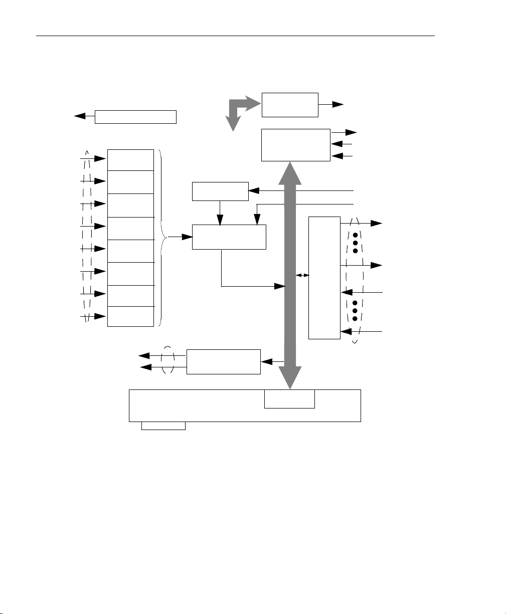
Figure 1 shows a block diagram of the KUSB-3100 module.
+2.5 V Reference
8-Channel Multiplexer
A/D Ch7
A/D Ch6
A/D Ch5
A/D Ch4
A/D Ch3
A/D Ch2
A/D Ch1
A/D Ch0
ESD Protected to 4000 V
DAC 1
DAC 0
From USB
Por t
A/D Clock
12-Bit A/D
Converter
12-Bit D/A
Converter
Power
Supply
32-Bit
Counter/Timer
+5 V
C/T Out 0
C/T Gate 0
C/T In 0
External Clock
External Trigger
Digital
I/O
ESD Protected to 4000 V
DOUT7
DOUT0
DIN7
DIN0
USB 2.0 or 1.1
Por t
Input FIFO
Figure 1: Block Diagram of the KUSB-3100 Module
6
Page 21

Analog Input Features
This section describes the following features of analog input (A/D)
operations on the KUSB-3100 module:
• Analog input channels, described on this page;
• Input resolution, described on page 8;
• Input ranges and gains, described on page 9;
Principles of Operation
2
2
• Input sample clock sources, described on page 10;
• Analog input conversion modes, described on page 11;
• Input triggers, described on page 13;
• Data format and transfer, described on page 14; and
• Error conditions, described on page 15.
Analog Input Channels
The KUSB-3100 module provides eight single-ended analog input
channels. The module can acquire data from a single analog input
channel or from a group of analog input channels.
The following subsections describe how to specify the channels.
Specifying a Single Analog Input Channel
The simplest way to acquire data from a single analog input channel
is to specify the channel for a single-value analog input operation
using software; refer to
single-value operations.
page 11 for more information about
2
2
2
2
2
2
You can also specify a single channel using the analog input
channel-gain list, described in the next section.
2
7
Page 22

Chapter 2
Specifying One or More Analog Input Channels
You can read data from one or more analog input channels using an
analog input channel-gain list. You can group the channels in the list
sequentially (starting either with 0 or with any other analog input
channel) or randomly. You can also specify a single channel or the
same channel more than once in the list.
Using software, specify the channels in the order you want to sample
them. You can enter up to 16 entries in the channel-gain list. The
channels are read in order from the first entry in the list to the last
entry in the list. Refer to
supported conversion modes.
The maximum rate at which the module can read the analog input
channels is 50
channels in the channel-gain list, the maximum sampling rate is
25
kSamples/s for each channel. Likewise, if you specify 16 analog
input channels in the channel-gain list, the maximum sampling rate is
3.125 kSamples/s for each channel.
kSamples/s. Therefore, if you specify two analog input
page 11 for more information about the
Input Resolution
The KUSB-3100 module provides a resolution of 12-bits. Note that the
resolution is fixed; it cannot be programmed in software.
8
Page 23

Input Ranges and Gains
Principles of Operation
The KUSB-3100 module features an input range of ±10 V. Use
software to specify the input range. Note that this is the range for the
entire analog input subsystem, not the range per channel.
The KUSB-3100 module supports programmable gains to allow many
more effective input ranges.
effective input ranges for each module.
Table 2: Effective Input Range
Gain Bipolar Input Range
1 ±10 V
2 ±5 V
4 ±2.5 V
8 ±1.25 V
For each channel on the KUSB-3100 module, choose the gain that has
the smallest effective range that includes the signal you want to
measure. For example, if your analog input signal ranges between
–2.0 V and +2.0, specify a gain of 4 for the channel; the effective input
range for this channel is then –2.5 V to +2.5
best sampling accuracy for that channel.
Table 2 lists the supported gains and
V, which provides the
2
2
2
2
2
2
2
The way you specify gain depends on how you specified the
channels, as described in the following subsections.
2
2
9
Page 24

Chapter 2
Specifying the Gain for a Single Channel
The simplest way to specify gain for a single channel is to specify the
gain for a single-value analog input operation using software; refer to
page 11 for more information about single-value operations.
You can also specify the gain for a single channel using an analog
input channel-gain list, described in the next section.
Specifying the Gain for One or More Channels
You can specify the gain for one or more analog input channels using
an analog input channel-gain list. Using software, set up the
channel-gain list by specifying the gain for each entry in the list.
For example, assume the analog input channel-gain list contains three
entries: channels 5, 6, and 7 and gains 2, 4, and 1. A gain of 2 is
applied to channel 5, a gain of 4 is applied to channel 6, and a gain of
1 is applied to channel 7.
10
Input Sample Clock Sources
You can use one of the following clock sources to pace an analog
input operation:
• Internal clock – Using software, specify the clock source as
internal and the clock frequency at which to pace the operation.
The minimum frequency of the internal clock is 30 Hz; the
maximum frequency of the internal clock is 50 kHz.
According to sampling theory (Nyquist Theorem), specify a
frequency that is at least twice as fast as the input’s highest
frequency component. For example, to accurately sample a 2 kHz
signal, specify a sampling frequency of at least 4 kHz. Doing so
avoids an error condition called aliasing, in which high frequency
input components erroneously appear as lower frequencies after
sampling.
Page 25

Principles of Operation
• External clock – An external clock is useful when you want to
pace acquisitions at rates not available with the internal clock or
when you want to pace at uneven intervals. The minimum
frequency of the external clock can be less than 30 Hz; the
maximum frequency of the external clock is 50 kHz.
2
Connect an external clock to the Ext Clock In signal on the
KUSB-3100 module. Conversions start on the rising edge of the
external clock input signal.
Using software, specify the clock source as external. The clock
frequency is always equal to the frequency of the external sample
clock input signal that you connect to the module.
Analog Input Conversion Modes
The KUSB-3100 module supports the following conversion modes:
• Single-value operations, described on this page.
• Continuous scan operations, described on page 12.
Single-Value Operations
Single-value operations are the simplest to use. Using software, you
specify the range, gain, and analog input channel. The module
acquires the data from the specified channel and returns the data
immediately. For a single-value operation, you cannot specify a clock
source, trigger source, scan mode, or buffer.
2
2
2
2
2
2
Single-value operations stop automatically when finished; you
cannot stop a single-value operation.
2
2
11
Page 26

Chapter 2
Continuous Scan Mode
Use continuous scan mode if you want to accurately control the
period between conversions of individual channels in a channel-gain
list.
When it receives a software trigger, the module cycles through the
channel-gain list, acquiring and converting the data for each entry in
the list (this process is defined as the scan). The module then wraps to
the start of the channel-gain list and repeats the process continuously
until either the allocated buffers are filled or until you stop the
operation. Refer to
The conversion rate is determined by the frequency of the internal
sample clock; refer to
sample clock. The sample rate, which is the rate at which a single
entry in the channel-gain list is sampled, is determined by the
frequency of the input sample clock divided by the number of entries
in the channel-gain list.
To select continuous scan mode, use software to specify the data flow
as continuous.
page 14 for more information about buffers.
page 10 for more information about the internal
12
Figure 2 illustrates continuous scan mode using a channel-gain list
with three entries: channel 0, channel 1, and channel 2. In this
example, analog input data is acquired on each clock pulse of the
input sample clock. When it reaches the end of the channel-gain list,
the module wraps to the beginning of the channel-gain list and
repeats this process. Data is acquired continuously.
Page 27
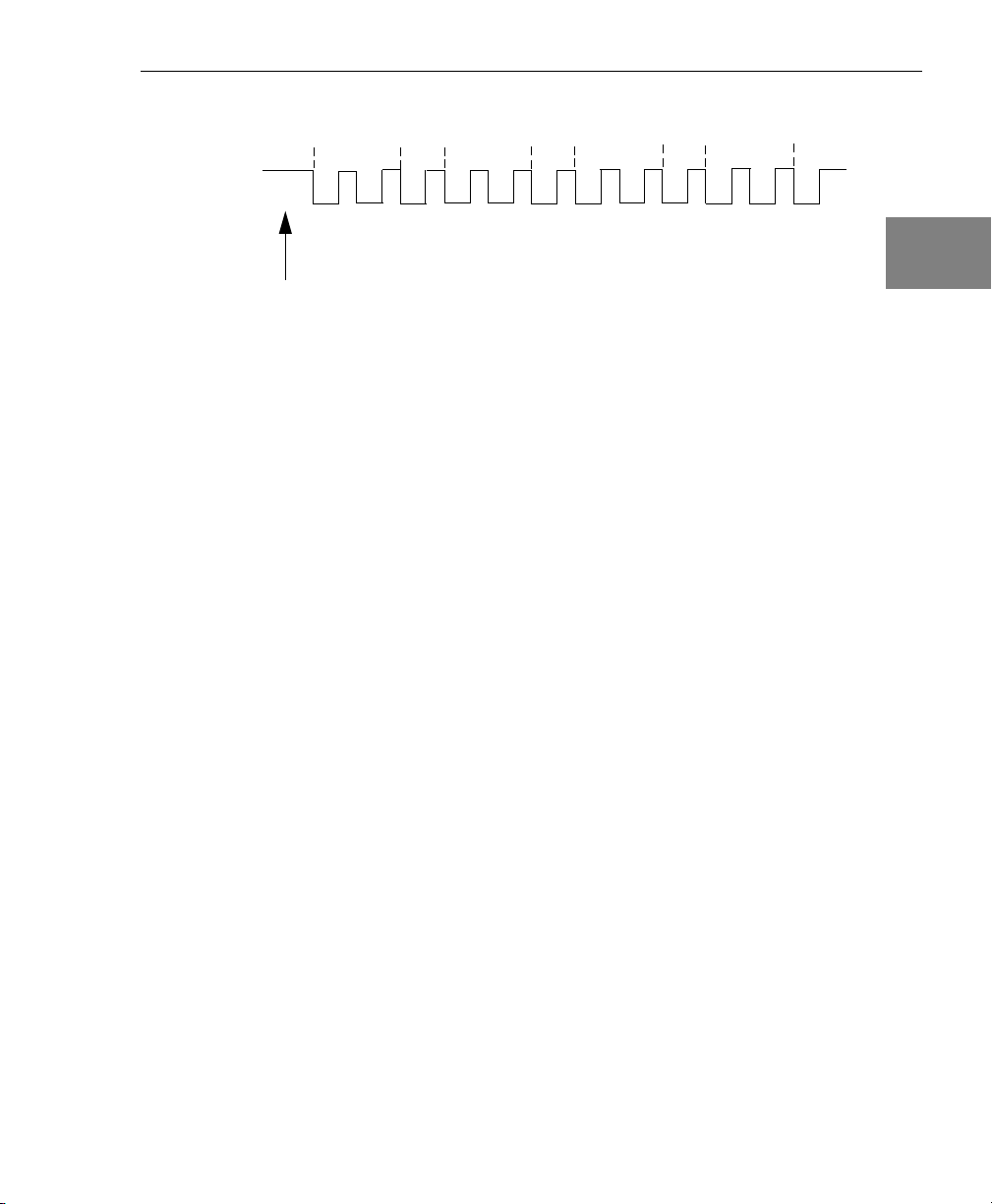
Principles of Operation
Chan 0
Chan 1
Input
Sample
Clock
Initial trigger event occurs
Figure 2: Continuous Scan Mode
Input Triggers
A trigger is an event that occurs based on a specified set of
conditions. Acquisition starts when the module detects the initial
trigger event and stops when the specified number of samples has
been acquired (if the buffer wrap mode is none, described on
14), or when you stop the operation. Note that when you stop the
operation, the module completes the reading of the channel-gain list.
The KUSB-3100 module supports the following trigger sources:
• Software trigger – A software trigger event occurs when you
start the analog input operation (the computer issues a write to
the module to begin conversions). Using software, specify the
trigger source as a software trigger.
• External digital (TTL) trigger – An external digital (TTL) trigger
event occurs when the module detects a high-to-low transition on
the Ext Trig In signal connected to the module. Using software,
specify the trigger source as a falling-edge external digital trigger
(trigger source extra).
Chan 2
Chan 0
Chan 1
Chan 2
Data acquired continuously
Chan 0
Chan 2
Chan 1
Chan 0
Chan 1
Chan 2
page
2
2
2
2
2
2
2
2
2
13
Page 28

Chapter 2
Data Transfer
Before you begin acquiring data, you must allocate buffers to hold
the data. During acquisition, a Buffer Done message is returned
whenever a buffer is filled. This allows you to move and/or process
the data as needed.
It is recommended that you allocate a minimum of three buffers for
analog input operations, specifying one of the following buffer wrap
modes in software:
• None – Data is written to multiple allocated input buffers
continuously; when no more empty buffers are available, the
operation stops. This wrap mode guarantees gap-free data.
• Multiple – Data is written to multiple allocated input buffers
continuously; if no more empty buffers are available, the module
overwrites the data in the current buffer, starting with the first
location in the buffer. This process continues indefinitely until
you stop it. This mode does not guarantee gap-free data.
14
Data Format
The KUSB-3100 module uses twos complement encoding to represent
bipolar input ranges. In software, the analog input value is returned
as a code.
To convert a twos complement code into a voltage, use the following
formulas:
LSB = FSR = 20 V = 0.0048828 V
2N 4096
Code
Offset Binary
= Code
Twos Complement
XOR 2
N-1
Page 29

Principles of Operation
Vin = Code
where,
• FSR is the full-scale range (20 V).
• N is the input resolution (12 bits).
• LSB is the least significant bit (0.0048828 V).
• Vin is the analog voltage.
• Code
represent the voltage in twos complement notation.
• Offset is the actual minus full-scale value (–10 V).
• Code
the voltage in offset binary notation.
For example, assume that the software returns a code of 3072 for the
analog input value. Determine the analog input voltage as follows:
Code
Code
Vin = 1024 * 0.0048828 V + –10 V
Offset Binary
Twos Com p lem ent
OffsetBinary
Offset Binary
Offset Binary
* LSB + Offset
is the raw count used by the software to
is the raw count used by the software to represent
= Code
= 3072 XOR 2048 = 1024
Twos Complement
XOR 2
N-1
2
2
2
2
2
2
Vin = –5.00 V
Error Conditions
An overrun condition is reported if the A/D sample clock rate is too
fast. This error is reported if a new A/D sample clock pulse occurs
while the ADC is busy performing a conversion from the previous
A/D sample clock pulse. It is up to the host application to handle this
error either by ignoring the error or stopping acquisition. To avoid
this error, use a slower sampling rate.
2
2
2
15
Page 30

Chapter 2
Analog Output Features
This section describes the following features of analog output
operations:
• Analog output channels, described on this page;
• Output resolution, described on page 17;
• Output ranges and gains, described on page 17;
• Output trigger, described on page 17,
• Output clock, described on page 18,
• Data format and transfer, described on page 21; and
• Error conditions, described on page 22.
Analog Output Channels
The KUSB-3100 module provides two analog output channels
(DACs). The module can output data from a single analog output
channel or from both analog output channels.
16
The following subsections describe how to specify the channels.
Specifying a Single Analog Output Channel
The simplest way to output data from a single analog output channel
is to use single-value analog output mode, specifying the analog
output channel that you want to update; refer to
information about single-value operations.
You can also specify a single analog output channel using the output
channel list, described in the next section.
page 18 for more
Page 31

Specifying Analog Output Channels
Principles of Operation
You can output data continuously from one or both analog output
channels using the output channel list. If you want to output data
from one analog output channel continuously, specify either 0
(DAC0) or 1 (DAC1) in the channel output list. If you want to output
data to both analog output channels continuously, specify the output
channel list in the following order: 0, 1.
Then, use software to specify the data flow mode as continuous for
the D/A subsystem; refer to
continuous analog output operations.
page 18 for more information on
Output Resolution
The KUSB-3100 module provides a fixed output resolution of 12 bits.
Note that the resolution is fixed; it cannot be programmed in
software.
Output Ranges and Gains
The KUSB-3100 module provides a fixed output range of ±10 V (the
gain is ignored).
2
2
2
2
2
2
Output Trigger
A trigger is an event that occurs based on a specified set of
conditions. The KUSB-3100 module supports a software trigger for
starting analog output operations. The module starts outputting data
when it receives a software command (trigger).
Use software to specify the trigger source for the D/A subsystem as a
software trigger.
2
2
2
17
Page 32

Chapter 2
Output Clock
When in continuous output mode, described on page 19, you can
update both analog output channels simultaneously using the
internal clock on the KUSB-3100 module.
Using software, specify the clock source for the D/A subsystem as
internal and specify a frequency between 30 Hz to 50 kHz at which to
update the analog output channels.
Note: The output clock frequency that you specify is the frequency
at which both analog output channels are simultaneously updated.
Output Conversion Modes
The KUSB-3100 module supports the following output conversion
modes:
18
• Single-value output operations, described on this page.
• Continuous output operations, described on page 19.
Single-Value Operations
Single-value operations are the simplest to use but offer the least
flexibility and efficiency. Use software to specify the analog output
channel, and the value to output from the analog output channel.
Since a single-value operation is not clocked, you cannot specify a
clock source, trigger source, or buffer.
Single-value operations stop automatically when finished; you
cannot stop a single-value operation.
Page 33

Continuous Output Mode
Principles of Operation
Use continuously paced analog output mode if you want to
accurately control the period between D/A conversions or write a
waveform to one or more analog output channels.
Use software to configure the output channel list, as described on
page 16. Then, allocate a buffer that contains the values to write to the
analog output channels that are specified in the output channel list.
For example, if your output channel list contains DAC0 and DAC1,
specify your buffer as follows: first value for DAC0, first value for
DAC1, second value for DAC0, second value for DAC1, and so on.
When it receives the software trigger, the module starts writing
output values to the analog output channels specified in the output
channel list. The operation repeats continuously until either all the
data is output from the buffers (if buffer wrap mode is none) or you
stop the operation (if buffer wrap mode is multiple). Refer to
for more information about buffer modes.
Note: Make sure that the host computer transfers data to the analog
output channels fast enough so that they do not empty completely;
otherwise, an underrun error results.
page 21
2
2
2
2
2
2
To select continuously paced analog output mode, use software to
specify the data flow as continuous, the buffer wrap mode as none or
multiple, the trigger source and output clock as internal, and the
output clock frequency (between 30 Hz and 50 kHz).
2
2
2
19
Page 34

Chapter 2
To stop a continuously paced analog output operation, you can stop
sending data to the module, letting the module stop when it runs out
of data, or you can perform either an orderly stop or an abrupt stop
using software. In an orderly stop, the module finishes outputting the
specified number of samples, then stops; all subsequent triggers are
ignored. In an abrupt stop, the module stops outputting samples
immediately; all subsequent triggers are ignored.
Data Transfer
If you are using continuous output mode, you must allocate and fill
multiple buffers with the appropriate data before starting the
operation, and specify one of the following buffer wrap modes in
software:
• None – Data is written from multiple output buffers
continuously; when no more buffers of data are available, the
continuous output operation stops. This mode guarantees
gap-free data.
• Multiple – Data is written from multiple output buffers
continuously; when no more buffers of data are available, the
module returns to the first location of the first buffer and
continues writing data. This process continues indefinitely until
you stop it. This mode does not guarantee gap-free data.
20
A Buffer Done message is returned whenever the last value in a
buffer is output. This allows you to fill the buffer or provide a new
buffer, as needed.
Note: An underrun error can result if your buffer size is too small,
if you do not allocate enough buffers, or if your output frequency is
too fast.
Page 35

Data Format
Principles of Operation
The KUSB-3100 module uses twos complement encoding for analog
output values. In software, you need to supply a code that
corresponds to the analog output value to output.
To convert a voltage into a twos complement code, use the following
formulas:
LSB = FSR = 20 V = 0.0048828 V
2N 4096
Code
Offset Binary
LSB
Code
Twos Com ple men t
where,
• FSR is the full-scale range (20 V).
• N is the input resolution (12 bits).
• LSB is the least significant bit (0.0048828).
• Vout is the analog voltage.
= Vo u t – Offset
= Code
Offset Binary
XOR (2
N-1
)
2
2
2
2
2
2
• Offset is the actual minus full-scale value (–10.0 V).
• Code
• Code
0.0048828 V
OffsetBinary
the voltage in offset binary notation.
Twos Com p lem ent
represent the voltage in twos complement notation.
Code
Offset Binary
LSB
Code
OffsetBinary
is the raw count used by the software to represent
is the raw count used by the software to
= Vout – O f f s e t
= + 5 V – (–10 V) = 3072
2
2
2
21
Page 36

Chapter 2
Code
Twos Complement
Code
Twos Complement
Error Conditions
The KUSB-3100 module can report an underrun error if the data for
the analog output channels is not sent fast enough from the host
computer. It is up to the host application to handle this error either by
ignoring it or by stopping the output operation.
To avoid this error, try slowing down the output frequency,
increasing the output buffer size, or allocating more output buffers.
Note: If no new data is available to be output by the analog output
channels, the last value that was written to the analog output
channels continues to be output by the analog output channels.
= 3072 XOR 2048
= 1024
22
Page 37

Digital I/O Features
This section describes the following features of digital I/O
operations:
• Digital I/O lines, described on this page;
• Resolution, described on page 23, and
• Operation modes, described on page 24.
Principles of Operation
2
2
Digital I/O Lines
The KUSB-3100 module provides 8 dedicated digital input lines and 8
dedicated digital output lines.
Using DT-Open Layers, you can specify the digital line that you want
to read or write in a single-value digital I/O operation. Refer to
24 for more information about single-value operations.
A digital line is high if its value is 1; a digital line is low if its value is
0. On power up or reset, a low value (0) is output from each of the
digital output lines.
Note: You can also read or write to the digital I/O lines using direct
register calls. Refer to
calls.
Resolution
2
2
page
2
2
Appendix C for more information on these
2
2
The resolution of the digital ports on the KUSB-3100 module is fixed
at 8-bits.
2
23
Page 38

Chapter 2
Operation Modes
The KUSB-3100 module supports single-value digital I/O operations
only. For a single-value operation, use software to specify digital
input port A or digital output port A (the gain is ignored). Data is
then read from or written to the digital lines associated with that port.
Single-value operations stop automatically when finished; you
cannot stop a single-value operation.
24
Page 39

Counter/Timer Features
This section describes the following features of counter/timer (C/T)
operations:
• C/T channels, described on this page;
• C/T clock sources, described on page 26;
• Gate types, described on page 26;
Principles of Operation
2
2
• Pulse types and duty cycles, described on page 27; and
• C/T operation modes, described on page 28.
C/T Channels
The KUSB-3100 module provides one 32-bit counter/timer (16 bits in
rate generation mode). The counter accepts a C/T clock input signal
(pulse input signal) and gate input signal, and outputs a pulse signal
(clock output signal), as shown in
C/T Clock Input SIgnal
(internal or external)
Figure 3.
Counter
Gate Input Signal
(software or
external input)
Figure 3: Counter/Timer Channel
Pulse Output
Signal
2
2
2
2
2
2
2
25
Page 40

Chapter 2
C/T Clock Sources
The following clock sources are available for the counter/timers:
• Internal clock – The internal clock uses a 24 MHz time base.
Through software, specify the clock source as internal, and
specify the frequency at which to pace the counter/timer
operation. The frequency of the internal C/T clock can range
from 15 Hz to 12 MHz.
• External clock – An external clock is useful when you want to
pace counter/timer operations at rates not available with the
internal clock or if you want to pace at uneven intervals.
Connect an external clock with a maximum recommended
frequency of 6 MHz to the Counter 0 In signal on the KUSB-3100
module. Using software, specify the C/T clock source as external,
and specify a clock divider between 2 and 65536 to determine the
actual frequency at which to pace the counter/timer operation.
For example, if you connect a 6 MHz external C/T clock and use
a clock divider of 2, the resulting C/T output frequency is 3 MHz.
Counter/timer operations start on the falling edge of the Counter
0 In signal.
26
Gate Types
The edge or level of the Counter 0 Gate signal determines when a
counter/timer operation is enabled. Using software, you can specify
one of the following gate types:
• None – A software command enables any counter/timer
operation immediately after execution.
• Logic-high level external gate input – Enables a counter/timer
operation when Counter 0 Gate is high, and disables a
counter/timer operation when Counter 0 Gate is low. Note that
this gate type is used for event counting and rate generation
modes; refer to page 28 for more information about these modes.
Page 41

Principles of Operation
• Falling-edge external gate input – Enables a counter/timer
operation when a high-to-low transition is detected on the
Counter 0 Gate signal. In software, this is called a low-edge gate
type. Note that this gate type is used for edge-to-edge
measurement mode; refer to page 30 for more information about
these modes.
• Rising-edge external gate input – Enables a counter/timer
operation when a low-to-high transition is detected on the
Counter 0 Gate signal. In software, this is called a high-edge gate
type. Note that this gate type is used for edge-to-edge
measurement operations; refer to page 30 for more information
about these modes.
2
2
2
Pulse Duty Cycles
Counter/timer output signals from the KUSB-3100 module are
high-to-low going signals.
The duty cycle (or pulse width) indicates the percentage of the total
pulse output period that is active. In rate generation mode, the duty
cycle is fixed at 50% for the KUSB-3100 module.
high-to-low going output pulse with a duty cycle of 50%.
Total Pulse Period
high pulse
low pulse
Active Pulse Width
Figure 4: Example of a Pulse Output SIgnal with a 50% Duty Cycle
(High-to-Low Going)
Figure 4 illustrates a
2
2
2
2
2
2
27
Page 42

Chapter 2
Counter/Timer Operation Modes
The KUSB-3100 module supports the following counter/timer
operation modes:
• Event counting, described on this page.
• Frequency measurement, described on page 29.
• Edge-to-edge measurement, described on page 30.
• Rate generation, described on page 31.
Event Counting
Use event counting mode if you want to count the number of falling
edges that occur on Counter 0 In when the gate is active (high-level
gate or software gate). Refer to
specifying the active gate type.
You can count a maximum of 4,294,967,296 events before the counter
rolls over to 0 and starts counting again.
page 26 for information about
28
For event counting operations, use software to specify the
counter/timer mode as count, the C/T clock source as external, and
the active gate type as software or high-level.
Make sure that the signals are wired appropriately. Refer to the
KUSB-3100 Getting Started Manual for an example of connecting an
event counting application.
Page 43

Frequency Measurement
Principles of Operation
Using software, specify the counter/timer mode as count, the clock
source as external, and the time over which to measure the frequency.
To specify the duration, you can use the Windows timer (which uses
a resolution of 1 ms), or if you need more accuracy than the Windows
timer provides, you can connect a pulse of a known duration to the
Counter 0 Gate signal.
If you are using a known pulse for the duration, specify the active
gate in software (high level or low level). When the operation starts,
read the number of counts that occurred when the gate was active.
You can determine the measurement period using the following
equation:
Measurement period = 1 * Active Pulse Width
Clock Frequency
You can determine the frequency of the clock input signal using the
following equation:
Frequency Measurement = Number of Events
Measurement Period
2
2
2
2
2
2
Make sure that the signals are wired appropriately. Refer to the
KUSB-3100 Getting Started Manual for an example of connecting a
frequency measurement application.
2
2
2
29
Page 44

Chapter 2
Edge-to-Edge Measurement
Use edge-to-edge measurement mode if you want to measure the
time interval between a specified start edge and a specified stop edge.
The start edge can occur on the rising edge or the falling edge of the
Counter 0 Gate signal, and the stop edge can occur on the rising edge
or the falling edge of the Counter 0 Gate signal. When the start edge
is detected, the counter/timer starts incrementing and continues
incrementing until the stop edge is detected. The C/T then stops
incrementing until it is enabled to start another measurement. When
the operation is complete, you can read the value of the counter. You
can count a maximum of 4,294,967,296 events before the counter rolls
over to 0 and starts counting again.
You can use edge-to-edge measurement to measure the following
characteristics of a signal:
•Pulse width – The amount of time that a signal pulse is in a high
or a low state, or the amount of time between a rising edge and a
falling edge or between a falling edge and a rising edge. You can
calculate the pulse width as follows:
30
− Pulse width = Number of counts/24 MHz
•Period – The time between two occurrences of the same edge
(rising edge to rising edge, or falling edge to falling edge). You
can calculate the period as follows:
− Period = 1/Frequency
− Period = Number of counts/24 MHz
•Frequency – The number of periods per second. You can
calculate the frequency as follows:
− Frequency = 24 MHz/Number of Counts
Using software, specify the counter/timer mode as measure, the C/T
clock source as internal, the start edge as rising or falling gate, and
the stop edge as rising or falling gate.
Page 45

Make sure that the signals are wired appropriately. Refer to the
KUSB-3100 Getting Started Manual for an example of connecting an
edge-to-edge measurement application.
Rate Generation
Use rate generation mode to generate a continuous pulse output
signal from Counter 0 Out; this mode is sometimes referred to as
continuous pulse output or pulse train output.
Principles of Operation
2
2
The pulse output operation is enabled whenever the Counter 0 Gate
signal is active (high level, low level, or software gate). While the
pulse output operation is enabled, the counter outputs a high-to-low
going pulse with a pulse width of 50% continuously. As soon as the
operation is disabled, rate generation stops.
The period of the output pulse is determined by the C/T clock source
(either internal or external) and the clock divider used. You can
generate an output signal from Counter 0 Out with a frequency of
15
Hz to 12 MHz.
To specify rate generation mode, use software to specify the
counter/timer mode as rate, the C/T clock source as either internal or
external, the clock divider (2 to 65536), and the active gate type
(high-level or software gate). Refer to
about gate types.
Make sure that the signals are wired appropriately. Refer to the
KUSB-3100 Getting Started Manual for an example of connecting a rate
generation application.
page 26 for more information
2
2
2
2
2
2
2
31
Page 46

Chapter 2
32
Page 47

3
Supported Device Driver
Capabilities
33
Page 48

Chapter 3
The device driver for the KUSB-3100 module supports A/D, D/A,
DIN, DOUT, and C/T subsystems. For information on how to
configure the device driver, refer to the KUSB-3100 Getting Started
Manual.
Table 3 summarizes the features available for use with the DataAcq
SDK and the KUSB-3100 module. The DataAcq SDK provides
functions that return support information for specified subsystem
capabilities at run-time.
The first row in the table lists the subsystem types. The first column
in the table lists all possible subsystem capabilities. A description of
each capability is followed by the parameter used to describe that
capability in the DataAcq SDK.
Note: Blank fields represent unsupported options.
The DataAcq SDK uses the functions olDaGetSSCaps (for those
queries starting with OLSSC) and olDaGetSSCapsEx (for those
queries starting with OLSSCE) to return the supported subsystem
capabilities for a device.
34
For more information, refer to the description of these functions in
the DataAcq SDK online help. See the DataAcq User’s Manual for
information on launching this help file.
Page 49

Supported Device Driver Capabilities
Table 3: KUSB-3100 Supported Options
KUSB-3100 A/D D/A DIN DOUT SRL C/T
3
Total Subsystems on Module 1 1 1
Single-Value Operation Support
OLSSC_SUP_SINGLEVALUE
Continuous Operation Support
OLSSC_SUP_CONTINUOUS
Continuous Operation until Trigger Event
Support
OLSSC_SUP_CONTINUOUS_PRETRIG
Continuous Operation before and after
Trigger Event
OLSSC_SUP_CONTINUOUS_
ABOUTTRIG
Data Flow Mode
DT-Connect Support
OLSSC_SUP_DTCONNECT
Continuous DT-Connect Support
OLSSC_SUP_DTCONNECT_
CONTINUOUS
Burst DT-Connect Support
OLSSC_SUP_DTCONNECT_BURST
Simultaneous Start List Support
OLSSC_SUP_SIMULTANEOUS_START Yes Yes
Sim.
Oper.
Pause Operation Support
OLSSC_SUP_PAUSE
Oper.
Pause
Asynchronous Operation Support
OLSSC_SUP_POSTMESSAGE
Wind.
Mess.
Buffer Support
OLSSC_SUP_BUFFERING
Single Buffer Wrap Mode Support
Buffering
OLSSC_SUP_WRPSINGLE
Ye s
Ye s
Ye s
Ye s
a
1b 0 1
Ye s
Ye s Ye s
Ye s Ye s
Ye s
Ye s Ye s
3
3
3
3
3
3
3
3
35
Page 50

Chapter 3
Table 3: KUSB-3100 Supported Options (cont.)
KUSB-3100 A/D D/A DIN DOUT SRL C/T
Total Subsystems on Module 1 1 1
Multiple Buffer Wrap Mode Support
OLSSC_SUP_WRPMULTIPLE
Inprocess Buffer Flush Support
OLSSC_SUP_INPROCESSFLUSH
Buffering (cont.)
Number of DMA Channels
OLSSC_NUMDMACHANS
Supports Gap Free Data with No DMA
OLSSC_SUP_GAPFREE_NODMA
DMA
Supports Gap Free Data with Single DMA
OLSSC_SUP_GAPFREE_SINGLEDMA
Supports Gap Free Data with Dual DMA
OLSSC_SUP_GAPFREE_DUALDMA
Triggered Scan Support
OLSSC_SUP_TRIGSCAN
Maximum Number of CGL Scans per
Trigger
OLSSC_MAXMULTISCAN
Supports Scan per Trigger Event
Triggered Scan
OLSSC_SUP_RETRIGGER_SCAN_
PER_TRIGGER
Supports Internal Retriggered Triggered
Triggered Scan Mode
Scan
OLSSC_SUP_RETRIGGER_INTERNAL
Extra Retrigger Support
OLSSC_SUP_RETRIGGER_EXTRA
Ye s
Ye s
0
Ye s
1
Ye s
0
0
a
0 0
0
1b 01
0
0
0
36
Page 51

Supported Device Driver Capabilities
Table 3: KUSB-3100 Supported Options (cont.)
KUSB-3100 A/D D/A DIN DOUT SRL C/T
Total Subsystems on Module 1 1 1
Maximum Retrigger Frequency
OLSSCE_MAXRETRIGGER 0 0
Minimum Retrigger Frequency
Tr ig. Sc a n
OLSSCE_MINRETRIGGER 0 0
Mode (cont.)
Maximum Channel-Gain List Depth
OLSSC_CGLDEPTH
Sequential Channel-Gain List Support
OLSSC_SUP_SEQUENTIAL_CGL
Zero Start Sequential Channel-Gain List
Support
OLSSC_SUP_ZEROSEQUENTIAL_CGL
Random Channel-Gain List Support
OLSSC_SUP_RANDOM_CGL
Channel-Gain List
Simultaneous Sample-and-Hold Support
OLSSC_SUP_SIMULTANEOUS_SH
Channel List Inhibit Support
OLSSC_SUP_CHANNELLIST_
INHIBIT
Programmable Gain Support
OLSSC_SUP_PROGRAMGAIN
Number of Gains
OLSSC_NUMGAINS
Gain
AutoRanging Support
OLSSC_SINGLEVALUE_AUTORANGE
Synchronous Digital I/O Support
OLSSC_SUP_SYNCHRONOUS_
DIGITALIO
Maximum Synchronous Digital I/O Value
Digital I/O
Synchronous
OLSSC_MAXDIGITALIOLIST_VALUE 0
16
Ye s
Ye s
Ye s
Ye s
c
4
2
Ye s
Ye s
1
0
a
0 0
0 0
0 0
1 1
0 0
1b 01
0
0
0
0
0
3
3
3
3
3
3
3
3
3
37
Page 52

Chapter 3
Table 3: KUSB-3100 Supported Options (cont.)
KUSB-3100 A/D D/A DIN DOUT SRL C/T
Total Subsystems on Module 1 1 1
Number of Channels
OLSSC_NUMCHANNELS
8
2
a
1 1
1b 01
Channel Expansion Support
OLSSC_SUP_EXP2896
I/O Channels
Channel Expansion
OLSSC_SUP_EXP727
SE Support
OLSSC_SUP_SINGLEENDED
SE Channels
OLSSC_MAXSECHANS
Ye s Ye s
8
2
0 0
DI Support
OLSSC_SUP_DIFFERENTIAL Yes Yes Yes
Channel Type
DI Channels
OLSSC_MAXDICHANS
1 1
Filter/Channel Support
OLSSC_SUP_FILTERPERCHAN
Number of Filters
Filters
OLSSC_NUMFILTERS
Number of Voltage Ranges
OLSSC_NUMRANGES
Range per Channel Support
Ranges
OLSSC_SUP_RANGEPERCHANNEL
1
c
1
1
1
1 1
0 0
Software Programmable Resolution
OLSSC_SUP_SWRESOLUTION
Number of Resolutions
Resolution
OLSSC_NUMRESOLUTIONS
d
1
d
1
e
e
1
1
Binary Encoding Support
OLSSC_SUP_BINARY Yes Yes Yes
Data
Twos Complement Support
Encoding
OLSSC_SUP_2SCOMP Yes
f
Ye s
f
1
0
1
0
0
1
38
Page 53

Supported Device Driver Capabilities
Table 3: KUSB-3100 Supported Options (cont.)
KUSB-3100 A/D D/A DIN DOUT SRL C/T
Total Subsystems on Module 1 1 1
Software Trigger Support
OLSSC_SUP_SOFTTRIG
External Trigger Support
OLSSC_SUP_EXTERNTRIG
Positive Threshold Trigger Support
OLSSC_SUP_THRESHTRIGPOS
Negative Threshold Trigger Support
OLSSC_SUP_THRESHTRIGNEG
Analog Event Trigger Support
Triggers
OLSSC_SUP_ANALOGEVENTTRIG
Digital Event Trigger Support
OLSSC_SUP_DIGITALEVENTTRIG
Timer Event Trigger Support
OLSSC_SUP_TIMEREVENTTRIG
Number of Extra Triggers
OLSSC_NUMEXTRATRIGGERS
Internal Clock Support
OLSSC_SUP_INTCLOCK
External Clock Support
OLSSC_SUP_EXTCLOCK
Simultaneous Input/Output on a Single
Clock Signal
OLSSC_SUP_SIMULTANEOUS_
CLOCKING Yes
Clocks
Number of Extra Clocks
OLSSC_NUMEXTRACLOCKS
Base Clock Frequency
OLSSCE_BASECLOCK
Maximum External Clock Divider
OLSSCE_MAXCLOCKDIVIDER
Ye s
Ye s
g
1
Ye s
Ye s
0
24 MHz 24 MHz 0 0
1
Ye s
g
0
Ye s
0
1
a
1b 01
Ye s
Ye s
0 0
0 0
1 1 65536
0
Ye s
Ye s
0
24 MHz
3
3
3
3
3
3
3
3
3
39
Page 54

Chapter 3
Table 3: KUSB-3100 Supported Options (cont.)
KUSB-3100 A/D D/A DIN DOUT SRL C/T
Total Subsystems on Module 1 1 1
Minimum External Clock Divider
OLSSCE_MINCLOCKDIVIDER
Maximum Throughput
OLSSCE_MAXTHROUGHPUT 50 kHz 50 kHz 0 0
Minimum Throughput
Clocks (cont.)
OLSSCE_MINTHROUGHPUT
Cascading Support
OLSSC_SUP_CASCADING
Event Count Mode Support
OLSC_SUP_CTMODE_COUNT
Generate Rate Mode Support
OLSSC_SUP_CTMODE_RATE
One-Shot Mode Support
OLSSC_SUP_CTMODE_ONESHOT
Repetitive One-Shot Mode Support
OLSSC_SUP_CTMODE_ONESHOT_
RPT
Up/Down Counting Mode Support
OLSC_SUP_CTMODE_UP_DOWN
Edge-to-Edge Measurement Mode
Counter/Timers
Support
OLSSC_SUP_CTMODE_MEASURE 3
Continuous Edge-to-Edge Measurement
Mode Support
OLSSC_SUP_CTMODE_CONT_
MEASURE
Fixed Pulse Width
OLSSC_FIXED_PULSE_WIDTH Yes
High to Low Output Pulse Support
OLSSC_SUP_PLS_HIGH2LOW
1
30 Hz 30 Hz 0 015 Hz
1
a
1 1
1b 01
2
12 MHz
Ye s
Ye s
h
i
Ye s
40
Page 55

Supported Device Driver Capabilities
Table 3: KUSB-3100 Supported Options (cont.)
KUSB-3100 A/D D/A DIN DOUT SRL C/T
Total Subsystems on Module 1 1 1
Low to High Output Pulse Support
OLSSC_SUP_PLS_LOW2HIGH
None (internal) Gate Type Support
OLSSC_SUP_GATE_NONE
High Level Gate Type Support
OLSSC_SUP_GATE_HIGH_LEVEL
Low Level Gate Type Support
OLSSC_SUP_GATE_LOW_LEVEL
High Edge Gate Type Support
OLSSC_SUP_GATE_HIGH_EDGE
Low Edge Gate Type Support
OLSSC_SUP_GATE_LOW_EDGE
Level Change Gate Type Suppor t
OLSSC_SUP_GATE_LEVEL
High Level Gate Type with Input
Debounce Support
OLSSC_SUP_GATE_HIGH_LEVEL_
DEBOUNCE
Counter/Timers (cont.)
Low Level Gate Type with Input
Debounce Support
OLSSC_SUP_GATE_LOW_LEVEL_
DEBOUNCE
High Edge Gate Type with Input
Debounce Support
OLSSC_SUP_GATE_HIGH_EDGE_
DEBOUNCE
Low Edge Gate Type with Input
Debounce Support
OLSSC_SUP_GATE_LOW_EDGE_
DEBOUNCE
a
1b 01
Ye s
Ye s
Ye s
Ye s
3
3
3
3
3
3
3
3
3
41
Page 56

Chapter 3
Table 3: KUSB-3100 Supported Options (cont.)
KUSB-3100 A/D D/A DIN DOUT SRL C/T
Total Subsystems on Module 1 1 1
Level Change Gate Type with Input
Debounce Support
(cont.)
OLSSC_SUP_GATE_LEVEL_
DEBOUNCE
Counter/Timers
Interrupt Support
OLSSC_SUP_INTERRUPT Yes
Interrupt
FIFO in Data Path Support
OLSSC_SUP_FIFO Yes
Output FIFO Size
FIFOs
OLSSC_FIFO_SIZE_IN_K 2
Data Processing Capability
OLSSC_SUP_PROCESSOR Yes Yes
Processor
Software Calibration Support
OLSSC_SUP_SWCAL Yes
Software
Calibration
a. The DIN subsystem contains eight digital input lines(0 to 7).
b. The DOUT subsystem contains eight digital output lines (0 to 7).
c. The KUSB-3100 module has a full-scale input range of ±10 V and supports gains of 1, 2, 4, and 8
to provide many effective input ranges. Refer to page 9 for more information on gains and
input ranges.
d. The KUSB-3100 module supports a fixed A/D and D/A resolution of 12-bits.
e. The resolution of the digital input port (port A) is fixed at 8-bits or eight digital input lines. The
resolution of the digital output port (port A) is fixed at 8-bits or eight digital output lines.
f. The KUSB-3100 module supports twos complement data encoding for the A/D and D/A
subsystems.
g. The external digital trigger input (trigger source is OL_TRG_EXTRA) is active on the falling
edge (high-to-low transition) of the TTL signal.
h. Edge-to-edge measurement is supported on the gate signal only; both rising and falling edges
are supported.
i. The pulse width (duty cycle) if fixed at 50% when rate generation mode is used.
j. A 2K FIFO is used by the D/A subsystem; a 1K FIFO is used by the A/D subsystem.
k. A calibration utility, described in Chapter 6, is provided for the KUSB-3100.
j
k
Ye s
k
a
1b 01
42
Page 57

4
Programming Flowcharts
Single-Value Operations . . . . . . . . . . . . . . . . . . . . . . . . . . . . . . . . . 45
Continuous A/D Operations . . . . . . . . . . . . . . . . . . . . . . . . . . . . . 47
Continuous D/A Operations . . . . . . . . . . . . . . . . . . . . . . . . . . . . . 49
Event Counting Operations . . . . . . . . . . . . . . . . . . . . . . . . . . . . . . 51
Frequency Measurement Operations . . . . . . . . . . . . . . . . . . . . . . 53
Edge-to-Edge Measurement Operations . . . . . . . . . . . . . . . . . . . 55
Pulse Output Operations. . . . . . . . . . . . . . . . . . . . . . . . . . . . . . . . . 57
Simultaneous Operations . . . . . . . . . . . . . . . . . . . . . . . . . . . . . . . . 59
43
Page 58

Chapter 4
The following flowcharts show the steps required to perform data
acquisition operations using DT-Open Layers. For illustration
purposes, the DataAcq SDK functions are shown; however, the
concepts apply to all DT-Open Layers software.
Note that many steps represent several substeps; if you are
unfamiliar with the detailed operations involved with any one step,
refer to the indicated page for detailed information. Optional steps
appear in shaded boxes.
44
Page 59

Single-Value Operations
Initialize the device driver and get the
device handle with olDaInitialize.
Get a handle to the subsystem with
olDaGetDASSa.
Programming Flowcharts
4
4
Set the data flow to
OL_DF_SINGLEVALUE using
olDaSetDataFlow.
For the A/D and D/A subsystems, set the
channel type to
OLSSC_SUP_SINGLEENDED using
olDaSetChannelType.
For the A/D and D/A subsystems, set the
data flow to OLSSC_SUP_2SCOMP for
twos complement data encoding using
olDaSetEncoding.
For the A/D and D/A subsystems,
set the range using olDaSetRange.
Go to the next page.
a
Specify A/D subsystem 0 for an analog input operation, D/A subsystem 0 for an analog
output operation, DIN subsystem 0 for a digital input operation, or DOUT subsystem 0 for a
digital output operation.
The resolution of the A/D and D/A subsystems is fixed at 12-bits. The resolution of the DIN
and DOUT subsystems is fixed at 8-bits.
Specify a range of –10 V to 10 V.
4
4
4
4
4
4
4
45
Page 60
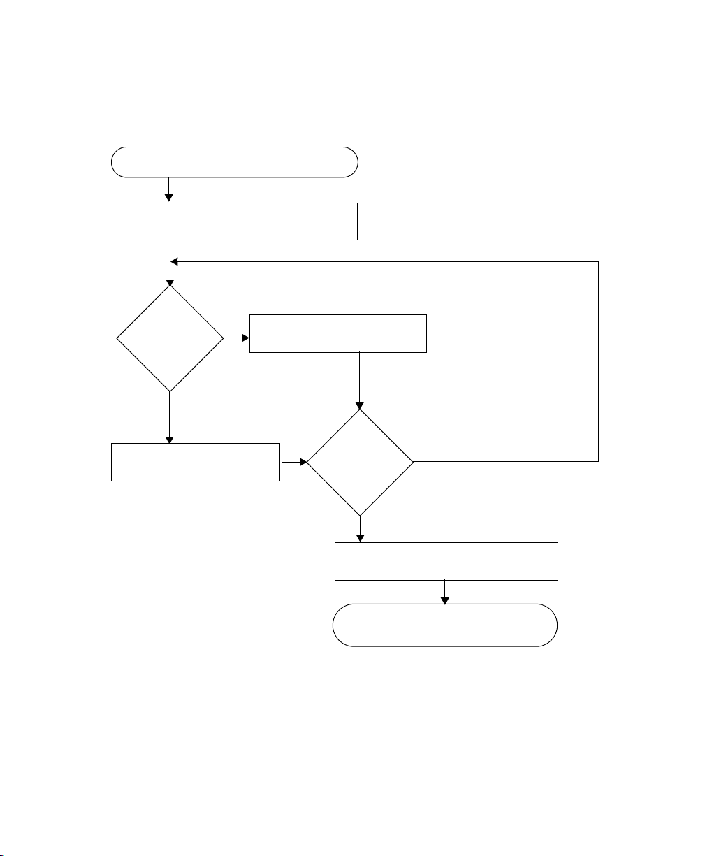
Chapter 4
Single-Value Operations (cont.)
Continued from previous page.
Configure the subsystem using
olDaConfig.
For the A/D subsystem, read a
single analog input value from
channel 0 to 7 using the
specified gain (1, 2, 4, or 8).
For the DIN subsystem, read
the value of the digital input
port.
Acquiring
data?
No
Ye s
Acquire a single value using
olDaGetSingleValue.
46
Output a single value using
olDaPutSingleValue.
For the D/A subsystem, output the
value to the specified analog
output channel (DAC0 or DAC1)
using a gain of 1. For the DOUT
subsystem, output a value to the
digital output port.
Acquire/
output
Ye s
another
value?
No
Release the subsystem using
olDaReleaseDASS.
Release the driver and terminate the
session using olDaTerminate.
Page 61

Continuous A/D Operations
Initialize the device driver and get the
device handle with olDaInitialize.
Programming Flowcharts
4
4
Get a handle to the A/D subsystem
with olDaGetDASS
Set the data flow using
olDaSetDataFlow.
Set the channel type to
OLSSC_SUP_SINGLEENDED using
olDaSetChannelType.
Set the data flow to
OLSSC_SUP_2SCOMP for twos
complement data encoding using
olDaSetEncoding.
Set the input range using
olDaSetRange.
Set up the analog input
channel-gain list (see page 61).
a
.
4
Specify OL_DF_CONTINUOUS (the
default value).
4
4
4
Specify a range of –10 V to 10 V.
4
Go to the next page.
a
Specify A/D subsystem 0 for an analog input operation. This subsystem supports analog
input channels 0 to 7. The resolution of the A/D subsystem is fixed at 12-bits.
4
4
47
Page 62

Chapter 4
Continuous A/D Operations (cont.)
Continued from previous page.
Set up the clocks and triggers
(see page 62).
Set up buffering (see page 63).
Configure the subsystem using
olDaConfig.
Start the operation with olDaStart.
Deal with messages and buffers
(see page 65).
Stop the operation (see page 70).
Clean up the operation (see page 71).
After you configure the subsystem, you can use
olDaGetClockFrequency to return the actual
frequency of the internal clock.
48
Page 63

Continuous D/A Operations
Initialize the device driver and get the
device handle with olDaInitialize.
Get a handle to D/A subsystem 0
with olDaGetDASSa.
Programming Flowcharts
4
4
4
Specify OL_DF_CONTINUOUS with
olDaSetDataFlow.
Set the channel type to
OLSSC_SUP_SINGLEENDED using
olDaSetChannelType.
Set the data flow to
OLSSC_SUP_2SCOMP for twos
complement data encoding using
olDaSetEncoding.
Set the output range using
olDaSetRange.
Set up the output channel list
(see page 61).
Go to the next page.
Continuous mode is the default setting.
4
4
4
Specify a range of –10 V to 10 V.
4
4
a
Specify D/A subsystem 0 for an analog output operation. This subsystem supports analog
output channels DAC0 and DAC1. The resolution of the D/A subsystem is fixed at 12-bits.
4
49
Page 64

Chapter 4
Continuous D/A Operations (cont.)
Continued from previous page.
Set up the clocks and triggers
(see page 62).
Set up buffering (see page 64).
Configure the subsystem using
olDaConfig.
Start the operation with olDaStart.
50
Deal with messages and buffers
(see page 65).
Stop the operation (see page 70).
Clean up the operation (see page 71).
Page 65
Event Counting Operations
Initialize the device driver and get the
device handle with olDaInitialize.
Programming Flowcharts
4
4
Get a handle to the C/T subsystem with
olDaGetDASS.
Specify the clock source as
OL_CLK_EXTERNAL using
olDaSetClockSource.
Specify the clock divider using
olDaSetExternalClockDivider
Specify the gate type as high-level
(OL_GATE_HIGH_LEVEL) or software
(OL_GATE_NONE) using
olDaSetGateType.
Specify the mode as OL_CTMODE_COUNT
using olDaSetCTMode.
Configure the subsystem using
olDaConfig.
Specify C/T subsystem/element 0.
4
Attach an external C/T with a maximum
recommended frequency of 6 MHz to
the Counter 0 In signal.
4
Specify a clock divider between 2 (the
default) and 65536.
4
4
4
Go to the next page.
4
4
51
Page 66

Chapter 4
Event Counting Operations (cont.)
Continued from previous page.
Start the operation using olDaStart.
Read the events counted using
olDaReadEvents.
Get update
of events
total?
No
Stop the operation (see page 70).
Release each subsystem with
olDaReleaseDASS.
Release the device driver and terminate
the session with olDaTerminate.
Ye s
52
Page 67

Programming Flowcharts
Frequency Measurement Operations
The following flowchart shows the steps required to perform a
frequency measurement operation using the Windows timer. If you
need more accuracy the Windows timer provides, refer to
this manual or to your DataAcq SDK User’s Manual for more
information.
4
page 23 of
4
Initialize the device driver and get the
device handle with olDaInitialize.
Get a handle to the C/T subsystem with
olDaGetDASS.
Specify the clock source as
OL_CLK_EXTERNAL using
olDaSetClockSource.
Specify the clock divider using
olDaSetExternalClockDivider
Specify the mode as OL_CTMODE_
COUNT using olDaSetCTMode.
Specify the gate type as high-level
(OL_GATE_HIGH_LEVEL) or software
(OL_GATE_NONE) using
olDaSetGateType.
Specify C/T subsystem/element 0.
Attach an external C/T with a maximum
recommended frequency of 6 MHz to
the Counter 0 In signal.
Specify a clock divider between 2 (the
default) and 65536.
4
4
4
4
4
4
Go to the next page.
4
53
Page 68
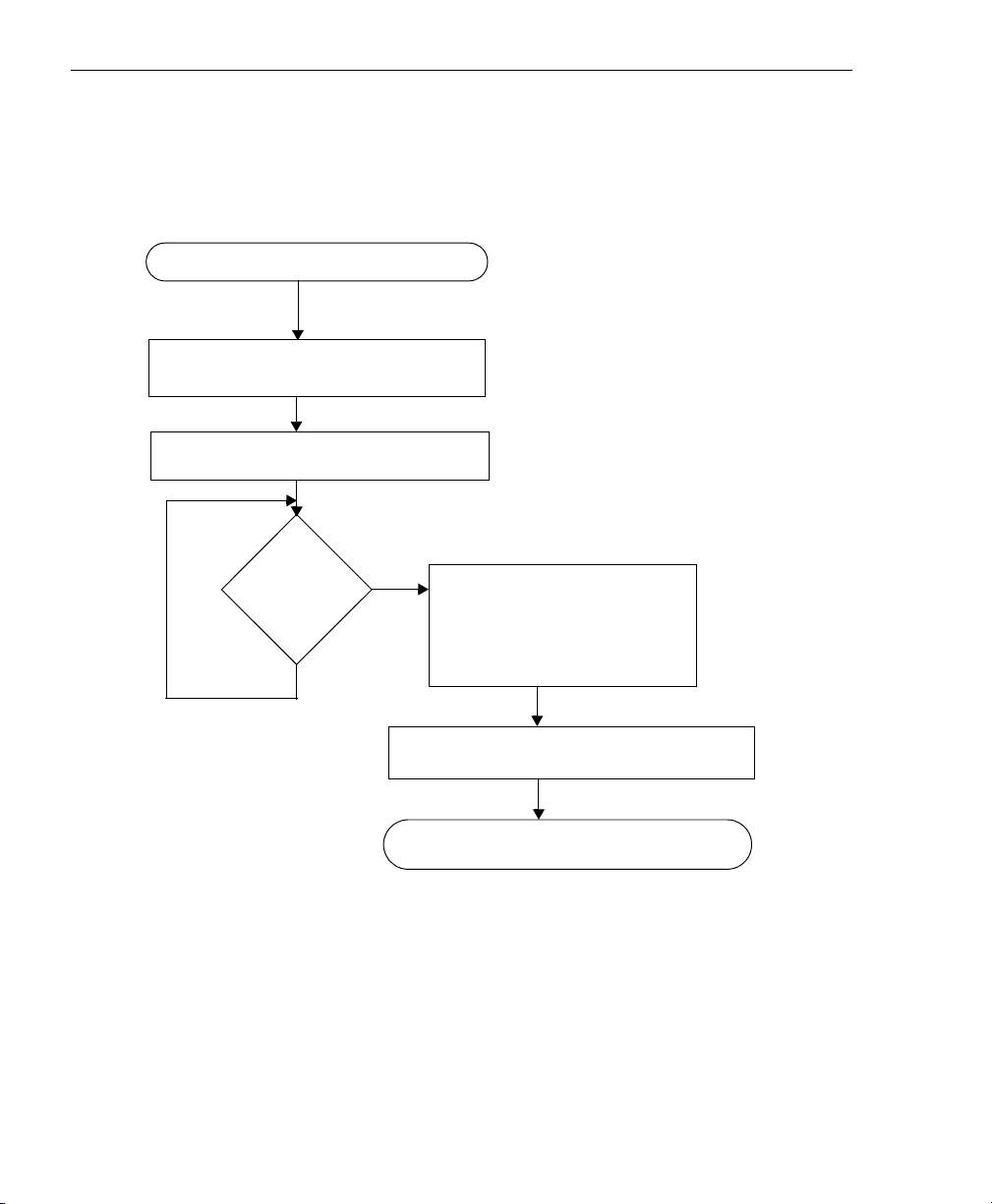
Chapter 4
Frequency Measurement Operations
(cont.)
Continued from previous page.
Configure the subsystem using
olDaConfig.
Start the frequency measurement
operation using olDaMeasureFrequency.
Message is in the form
Measure
done
message
returned?
No
Ye s
OLDA_WM_MEASURE_DONE.
Use the LongtoFreq (IParam)
macro to get the measured
frequency value:
float = Freq;
Freq = LongtoFreq (IParam);
54
Release each subsystem with
olDaReleaseDASS.
Release the device driver and terminate
the session with olDaTerminate.
Page 69

Programming Flowcharts
Edge-to-Edge Measurement Operations
Initialize the device driver and get the
device handle with olDaInitialize.
4
4
Get a handle to the C/T subsystem with
olDaGetDASS.
Specify the mode as
OL_CTMODE_MEASURE
using olDaSetCTMode.
Specify the clock source as
OL_CLK_INTERNAL using
olDaSetClockSource.
Specify the start edge
using olDaSetMeasureStartEdge.
Specify the stop edge
using olDaSetMeasureStopEdge.
Configure the subsystem using
olDaConfig.
Specify C/T subsystem/element 0.
4
4
4
Specify OL_GATE_RISING for a rising
edge on the Counter 0 Gate input or
OL_GATE_FALLING for a falling edge on
the Counter 0 Gate input.
4
Specify OL_GATE_RISING for a rising
edge on the Counter 0 Gate input or
OL_GATE_FALLING for a falling edge on
the Counter 0 Gate input.
4
Go to the next page.
4
4
55
Page 70

Chapter 4
Edge-to-Edge Measurement
Operations (cont.)
Continued from previous page.
Start the operation using olDaStart.
Message is in the form OLDA_WM_EVENT_DONE.
Note that if you want to perform another
edge-to-edge measurement, you can call olDaStart
again or use the OLDA_WM_EVENT_DONE
Event
done
message
returned?
No
handler to call olDaStart again.
Ye s
Read the value of the lParam
OLDA_WM_EVENT_DONE message
to determine the value of the counter.
Release each subsystem with
olDaReleaseDASS.
parameter in the
56
Release the device driver and terminate
the session with olDaTerminate.
Page 71

Pulse Output Operations
Initialize the device driver and get the
device handle with olDaInitialize.
Programming Flowcharts
4
4
Get a handle to the C/T subsystem with
olDaGetDASS.
Using an
internal clock?
No
Specify OL_CLK_EXTERNAL
using olDaSetClockSource.
Specify the clock divider using
olDaSetExternalClockDivider
Specify the gate type using
olDaSetGateType
Go to the next page.
Ye s
Specify OL_CLK_INTERNAL
using olDaSetClockSource.
Specify C/T subsystem/element 0.
Specify a frequency of
15 Hz to 12 MHz.
Attach an external C/T with a maximum
recommended frequency of 6 MHz to the
Counter 0 In signal.
Specify a clock divider between 2 (the
default) and 65536.
Specify OL_GATE_HIGH_LEVEL for a
high-level gate or OL_GATE_NONE for a
software gate.
4
4
4
4
4
4
4
57
Page 72
Chapter 4
Pulse Output Operations (cont.)
Continued from previous page.
Specify the mode using
olDaSetCTMode.
Specify the output pulse type using
olDaSetPulseType.
Configure the subsystem using
olDaConfig.
Start the operation using olDaStart.
Stop the operation (see page 70).
Release each subsystem with
olDaReleaseDASS.
Release the device driver and
terminate the session with
olDaTerminate.
Specify OL_CTMODE_RATE for rate
generation mode.
Must be a high-to-low pulse. The duty cycle is
fixed at 50%.
58
Page 73

Simultaneous Operations
Programming Flowcharts
4
Configure the A/D and D/A
subsystem that you want to run
simultaneously.
Allocate a simultaneous start list using
olDaGetSSList.
Put each subsystem to be
simultaneously started on the start list
using olDaPutDassToSSList.
Prestart the subsystems on the
simultaneous start list with
olDaSimultaneousPreStart.
Start the subsystems on the
simultaneous start list with
olDaSimultaneousStart.
Go to the next page.
See the previous flow diagrams in this
chapter; note that you cannot perform
single-value operations
simultaneously.
4
4
4
4
4
4
4
4
59
Page 74

Chapter 4
Simultaneous Operations (cont.)
Continued from previous page.
Deal with messages (see page 65 for
analog input operations; see page 68
for analog output operations).
Stop the operation (see page 70).
Clean up the operation
(see page 71).
60
Page 75

Set Up Channel List and Channel Parameters
Use to specify the size of the analog input channel-gain
olDaSetChannelListSize
olDaSetChannelListEntry
list (maximum of 16) or analog output channel list
(maximum of 2). The default value is 1.
Specify the channels in the A/D or D/A channel list. For
the A/D subsystem, channels 0 to 7 are available; you
can specify up to 16 channels in the channel-gain list.
For the D/A subsystem, channels 0 and 1 are available;
you can specify up to 2 channels in the output-channel
list. If you want to update both DACs, enter 0, then 1 in
the list.
Programming Flowcharts
4
4
4
4
4
olDaSetGainListEntry
For the A/D subsystem only, specify the gain for each
channel in the channel list (1, 2, 4,or 8).
For the D/A subsystem, use a gain of 1 (the default).
4
4
4
4
61
Page 76
Chapter 4
Set Clocks and Triggers
Using an
Ye s
internal
clock?
No
olDaSetClockSource
olDaSetTrigger
Specify OL_CLK_INTERNAL (the
olDaSetClockSource
olDaSetClockFrequency
For the A/D subsystem only, specify OL_CLK_EXTERNAL
to select the external clock. The D/A subsystem does not
support an external clock.
Specify OL_TRG_SOFT (the default) to select a software
trigger or OL_TRG_EXTRA to select a falling-edge external
digital (TTL) trigger. Only the A/D subsystem supports an
external trigger.
default) to select the internal clock.
Use to specify the frequency of the
internal clock. For the A/D and D/A
subsystems, values range from 30 Hz
to 50 kHz. The driver sets the actual
frequency as closely as possible to
the number specified.
62
Page 77
Set Up A/D Buffering
Programming Flowcharts
4
Using main
window to
handle
messages?
No
olDaSetWrapMode
olDmAllocBuffer
olDaPutBuffer
Ye s
olDaSetWndHandle
Use to specify the window in
which to post messages.
Use to specify the buffer wrap mode
(OL_WRP_NONE for guaranteed gap-free operation;
OL_WRP_ MULTIPLE for not guaranteed gap-free
operation).
Use to allocate a buffer of the specified number of
samples; each sample is 2 bytes.
Use to put the buffer on the ready queue.
4
4
4
4
4
4
Allocate
more
buffers?
Ye s
A minimum of three buffers is recommended.
4
4
63
Page 78

Chapter 4
Set Up D/A Buffering
Using main
window to
Ye s
handle
messages?
No
olDaSetWrapMode
olDmAllocBuffer
Fill the buffer.
olDmSetValidSamples
olDaSetWndHandle
Use to specify the buffer wrap mode
(OL_WRP_NONE if buffers are not reused or
OL_WRP_ MULTIPLE if all buffers are continuously
reused).
Use to allocate a buffer of the specified number of
samples; each sample is 2 bytes.
Fill the buffers with the data needed by your output
channel list. Refer to page 20 for more information.
Use to specify the valid number of data points in the
buffer.
Use to specify the window in
which to post messages.
64
olDaPutBuffer
Allocate
Ye s
more
buffers?
Use to put the buffer on the ready queue.
Page 79
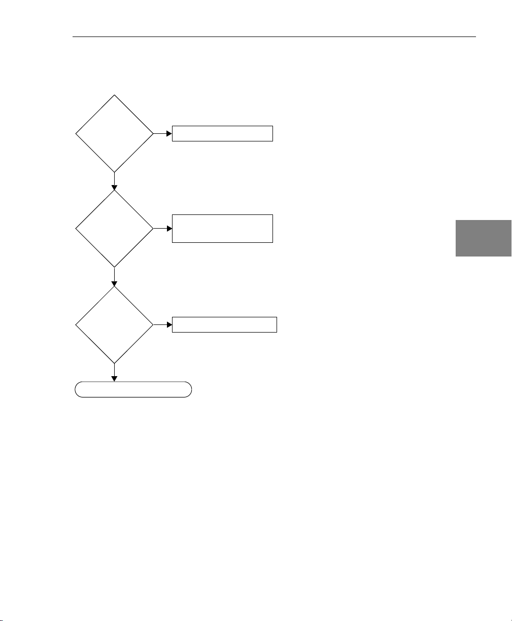
Deal with A/D Messages and Buffers
Programming Flowcharts
4
Error
returned?
No
Buffer
reused
message
returned?
No
Queue
message
returned?
No
Go to the next page.
Ye s
Ye s
Ye s
Report the error.
Increment a counter, if
desired.
Report the condition.
The most likely error message is
OLDA_WM_OVERRUN.
The buffer reused message is
OLDA_WM_BUFFER_REUSED.
The queue messages are
OLDA_WM_QUEUE_DONE and
OLDA_WM_QUEUE_STOPPED. After
reporting that the acquisition has stopped,
you can clean up the operation
(see page 71).
4
4
4
4
4
4
4
4
65
Page 80

Chapter 4
Deal with A/D Messages and Buffers (cont.)
Continued from previous page
The buffer done message is
OLDA_WM_BUFFER_DONE. Use
olDaGetBuffer to retrieve the buffer
from the done queue and get a
Buffer done
message
returned?
Ye s
Process
data?
Ye s
olDaGetBuffer
pointer to the buffer.
No
Wait for
message?
Ye s
No
Return to page 65.
olDmGetValidSamples
olDmGetValidSamples to determine
the number of samples in the buffer.
olDmCopyFromBuffer
Process the data/buffer in
your program.
olDaPutBuffer
Use
Use olDaPutBuffer to recycle the
buffer so that the subsystem can
fill it again. See the next page if
you want to transfer data from an
inprocess buffer.
66
Page 81

Transfer Data from an Inprocess Buffer
Programming Flowcharts
4
olDaGetQueueSize
olDmAllocBuffer
olDmCallocBuffer
olDmMallocBuffer
olDaFlushFromBufferInprocess
Deal with messages and
buffers.
Use to determine the number of buffers on the
inprocess queue (at least one must exist).
Use to allocate a buffer of the specified number of
samples.
Use to copy the data from the inprocess buffer to
the allocated buffer for immediate processing.
The buffer into which inprocess data was copied
was put onto the done queue by the driver,
resulting in an OLDA_WM_BUFFER_DONE
message. See page 65 for more information.
When the inprocess buffer has been filled, it too is
placed on the done queue and an
OLDA_WM_BUFFER_DONE message is posted.
However, the number of valid samples is equal to
the queue’s maximum samples minus what was
copied out.
4
4
4
4
4
4
4
4
67
Page 82

Chapter 4
Deal with D/A Messages and Buffers
Error
returned?
No
Buffer
reused
message
returned?
No
Queue
done
message
returned ?
No
Go to the next page.
Ye s
Report the error.
Ye s
Increment a counter, if
Ye s
Report the condition.
desired.
The most likely error messages include
OLDA_WM_UNDERRUN and
OLDA_WM_TRIGGER_ERROR.
The buffer reused message is
OLDA_WM_BUFFER_REUSED.
The queue done messages are
OLDA_WM_QUEUE_DONE and
OLDA_WM_QUEUE_STOPPED. After
reporting that the acquisition has stopped,
you can clean up the operation
(see page 71).
68
Page 83

Deal with D/A Messages and Buffers (cont.)
Programming Flowcharts
Continued from previous page
Buffer done
message
returned?
No
Ye s
Use new
data?
No
Ye s
olDaGetBuffer
olDmCopyToBuffer
olDaPutBuffer
The buffer done message is
OLDA_WM_BUFFER_
DONE. Use olDaGetBuffer
to retrieve a buffer from the
done queue and get a
pointer to the buffer.
Fill the buffer.
Use olDaPutBuffer to recycle the
buffer so that the subsystem can fill it
again (in OL_WRP_NONE or
OL_WRP_MULTIPLE mode only).
4
4
4
4
4
4
IO complete
message
returned?
No
Wait for
message?
Ye s
Ye s
The IO complete message is OLDA_WM_IO_COMPLETE.
It is generated when the last data point has been output
from the analog output channel. Note that in some cases,
this message is generated well after the data is transferred
from the buffer (when the OLDA_WM_BUFFER_DONE and
OLDA_WM_QUEUE_DONE messages are generated.
Return to page 66.
4
4
4
69
Page 84

Chapter 4
Stop the Operation
Stop in an
orderly
way?
No
Reinitialize?
No
olDaAbort
Ye s
Ye s
Waits until the last sample of
the current buffer is filled,
olDaStop
then stops. The driver posts
a Buffer Done and Queue
Stopped message.
olDaReset
Use olDaAbort and olDaReset to stop the operation
on the subsystem immediately; the valid samples are
marked and the buffer is placed on the done queue.
No messages are generated. In addition, olDaReset
reinitializes the subsystem to the driver’s default
state.
70
Page 85

Clean Up the Operation
Programming Flowcharts
4
olDaFlushFromBufferInprocess
olDaGetQueueSize
olDaGetBuffer
olDmFreeBuffer
More
buffers to
free?
No
olDaReleaseSSList
olDaReleaseDASS
olDaTerminate
Ye s
Use to flush all buffers on the ready and/or
inprocess queues to the done queue.
Use to determine the number of buffers on
the done queue.
Use to retrieve each buffer on the done
queue.
Use to free each buffer retrieved from the
done queue.
For simultaneous operations only, use to
release the simultaneous start list.
Use to release each subsystem.
Use to release the device driver and
terminate the session.
4
4
4
4
4
4
4
4
71
Page 86

Chapter 4
72
Page 87

5
Troubleshooting
General Checklist . . . . . . . . . . . . . . . . . . . . . . . . . . . . . . . . . . . . . . . 74
Service and Support. . . . . . . . . . . . . . . . . . . . . . . . . . . . . . . . . . . . . 77
73
Page 88

Chapter 5
General Checklist
Should you experience problems using a KUSB-3100 module, please
follow these steps:
1. Read all the documentation provided for your product. Make
sure that you have added any “Read This First” information to
your manual and that you have used this information.
2. Check the CD for any README files and ensure that you have
used the latest installation and configuration information
available.
3. Check that your system meets the requirements stated in the
KUSB-3100 Getting Started Manual.
4. Check that you have installed your hardware properly using the
instructions in the KUSB-3100 Getting Started Manual.
5. Check that you have installed and configured the device driver
properly using the instructions in the KUSB-3100 Getting Started
Manual.
74
If you still experience problems, try using the information in Table 4
to isolate and solve the problem. If you cannot identify the problem,
refer to
page 75.
Page 89

Table 4: Troubleshooting Problems
Symptom Possible Cause Possible Solution
Troubleshooting
5
Module does not
respond.
Intermittent
operation.
Device failure
error reported.
The module
configuration is
incorrect.
The module is
damaged.
Loose connections or
vibrations exist.
The module is
overheating.
Electrical noise exists. Check your wiring and either provide
The module cannot
communicate with the
Microsoft bus driver
or a problem with the
bus driver exists.
The module was
removed while an
operation was being
performed.
Check the configuration of your device
driver; see the instructions in the
KUSB-3100 Getting Started Manual.
Contact Keithley for technical support;
refer to page 77.
Check your wiring and tighten any loose
connections or cushion vibration sources;
see the instructions in the KUSB-3100
Getting Started Manual.
Check environmental and ambient
temperature; consult the module’s
specifications on
and the documentation provided by your
computer manufacturer for more
information.
better shielding or reroute unshielded
wiring; see the instructions in the
KUSB-3100 Getting Started Manual.
Check your cabling and wiring and tighten
any loose connections; see the
instructions in the KUSB-3100 Getting
Started Manual.
Ensure that your module is properly
connected; see the instructions in the
KUSB-3100 Getting Started Manual.
page 97 of this manual
5
5
5
5
5
5
5
5
75
Page 90

Chapter 5
Table 4: Troubleshooting Problems (cont.)
Symptom Possible Cause Possible Solution
Data appears to
be invalid.
Computer does
not boot.
An open connection
exists.
A transducer is not
connected to the
channel being read.
The module is set up
for differential inputs
while the transducers
are wired as
single-ended inputs
or vice versa.
The power supply of
the computer is too
small to handle all the
system resources.
Check your wiring and fix any open
connections; see the instructions in the
KUSB-3100 Getting Started Manual.
Check the transducer connections; see
the instructions in the KUSB-3100 Getting
Started Manual.
Check your wiring and ensure that what
you specify in software matches your
hardware configuration; see the
instructions in the KUSB-3100 Getting
Started Manual.
Check the power requirements of your
system resources and, if needed, get a
larger power supply; consult the module’s
specifications on
page 97 of this manual.
76
Page 91

Service and Support
For the latest tips, software fixes, and other product information, you
can always access our World-Wide Web site at the following address:
http://www.keithley.com
Troubleshooting
5
If you have difficulty using the KUSB-3100 module, Keithley’s
Technical Support Department is available to provide technical
assistance.
For the most efficient service, complete the form on page 78 and be at
your computer when you call for technical support. This information
helps to identify specific system and configuration-related problems
and to replicate the problem in house, if necessary.
5
5
5
5
5
5
5
5
77
Page 92

Chapter 5
Information Required for Technical Support
Name:___________________________________________Phone__________________________
Contract Number: __________________________________________________________________
Address: _________________________________________________________________________
________________________________________________________________________________
Hardware product(s): _______________________________________________________________
serial number: _________________________________________________________________
configuration: _________________________________________________________________
Device driver: ____________________________________ ________________________________
_______________________________________________ version: _________________________
Software:________________________________________ ________________________________
serial number: ________________________________ version:__________________________
PC make/model: ___________________________________________________________________
operating system: _____________________________ version:__________________________
Windows version: ______________________________________________________________
processor: ___________________________________ speed:___________________________
RAM: _______________________________________ hard disk space:____________________
network/number of users: _______________________ disk cache:________________________
graphics adapter: _____________________________ data bus:_________________________
I have the following boards and applications installed in my system:____________________________
________________________________________________________________________________
________________________________________________________________________________
I am encountering the following problem(s): ______________________________________________
________________________________________________________________________________
________________________________________________________________________________
________________________________________________________________________________
and have received the following error messages/codes: ____________________________________
________________________________________________________________________________
________________________________________________________________________________
I have run the board diagnostics with the following results: __________________________________
________________________________________________________________________________
You can reproduce the problem by performing these steps:
1. _______________________________________________________________________________
________________________________________________________________________________
2. _______________________________________________________________________________
________________________________________________________________________________
3. _______________________________________________________________________________
________________________________________________________________________________
78
Page 93

6
Calibration
Using the KUSB-3100 Calibration Utility . . . . . . . . . . . . . . . . . . . 81
Calibrating the Analog Input Subsystem . . . . . . . . . . . . . . . . . . . 82
Calibrating the Analog Output Subsystem . . . . . . . . . . . . . . . . . 85
79
Page 94

Chapter 6
The KUSB-3100 module is calibrated at the factory and should not
require calibration for initial use. It is recommended that you check
and, if necessary, readjust the calibration of the analog input and
analog output circuitry on the KUSB-3100
using the KUSB-3100 Calibration Utility.
Note: Ensure that you installed the KUSB-3100 Device Driver prior
to using the KUSB-3100 Calibration Utility. Refer to the KUSB-3100
Getting Started Manual for more information on installing the device
driver.
This chapter describes how to calibrate the analog input and output
subsystems of a KUSB-3100 module using the KUSB-3100 Calibration
Utility.
modules every six months
80
Page 95

Using the KUSB-3100 Calibration Utility
Start the KUSB-3100 Calibration Utility by performing the following
steps:
1. Locate the KUSB-3100 program folder on your hard disk.
Calibration
6
2. Double-click KUSB-3100 Calibration.Exe in the program folder.
The main menu appears.
3. Select the module to calibrate, then click OK.
Once the KUSB-3100 Calibration Utility is running, you can calibrate
the analog input circuitry (either automatically or manually),
described on
module, described on page 85.
page 82, or the analog output circuitry of the KUSB-3100
6
6
6
6
6
6
6
6
81
Page 96

Chapter 6
Calibrating the Analog Input Subsystem
This section describes how to use the KUSB-3100 Calibration Utility
to calibrate the analog input subsystem of a KUSB-3100 module.
Connecting a Precision Voltage Source
To calibrate the analog input circuitry, you need to connect an
external precision voltage source to Analog In 0 (AD Ch0) of the
KUSB-3100 module.
Using the Auto-Calibration Procedure
Auto-calibration is the easiest to use and is the recommended
calibration method. To auto-calibrate the analog input subsystem,
perform the following steps:
1. Select the A/D Configuration tab of the KUSB-3100 Calibration
Utility.
2. Set the voltage supply on AD Ch0 to 0 V.
82
3. Click Start Auto Calibration.
A message appears notifying you to verify that 0 V is applied to AD
Ch0.
4. Check that the supplied voltage to AD Ch0 is 0V, then click OK.
The offset value is calibrated. When the offset calibration is complete, a
message appears notifying you to set the input voltage of AD Ch 0 to
+9.375
V.
5. Check that the supplied voltage to AD Ch0 is +9.375V, then click
OK.
The gain value is calibrated.
6. Click OK to finalize the analog input calibration process.
Page 97

Calibration
Note: At any time, you can click Restore Factory Settings to reset
the A/D calibration values to their original factory settings. This
process will undo any auto or manual calibration settings.
Using the Manual Calibration Procedure
If you want to manually calibrate the analog input circuitry instead of
auto-calibrating it, perform the following steps:
1. Adjust the offset by performing the following steps:
a. Verify that 0V is applied to AD Ch0, and that A/D Channel
Select is set to Channel 0.
The current voltage reading for this channel is displayed in the A/D
Value windo w.
b. Adjust the offset by entering values between 0 and 63 in the
Offset edit box, or by clicking the up/down buttons until the
A/D Value is 0 V.
2. Adjust the gain by performing the following steps:
a. Verify that 9.375V is applied to AD Ch0, and that A/D
Channel Select is set to Channel 0.
The current voltage reading for this channel is displayed in the A/D
Value windo w.
6
6
6
6
6
6
b. Adjust the gain by entering values between 0 and 63 in the
Gain edit box, or by clicking the up/down buttons until the
A/D Value is 9.3750.
6
6
6
83
Page 98

Chapter 6
Note: At any time, you can click Restore Factory Settings to reset
the A/D calibration values to their original factory settings. This
process will undo any auto or manual calibration settings.
Once you have finished this procedure, continue with “Calibrating
the Analog Output Subsystem” on page 85.
84
Page 99

Calibrating the Analog Output Subsystem
This section describes how to use the KUSB-3100 Calibration Utility
to calibrate the analog output subsystem of a KUSB-3100 module.
To calibrate the analog output circuitry, you need to connect an
external precision voltmeter to analog output channels 0 and 1 of the
KUSB-3100 module.
Perform the following steps to calibrate the analog output circuitry:
Calibration
6
6
1. Select the D/A Configuration tab of the KUSB-3100 Calibration
Utility.
2. Connect an external precision voltmeter to Analog Output 0
(DAC Ch0) of the KUSB-3100 module.
3. Adjust the offset by entering values between 0 and 63 in the DAC
0 Offset edit box or by clicking the up/down buttons until the
voltmeter reads 0 V.
4. Connect an external precision voltmeter to Analog Output 1
(DAC Ch1) of the KUSB-3100 module.
5. Adjust the offset by entering values between 0 and 63 in the
DAC 1 Offset edit box or by clicking the up/down buttons until
the voltmeter reads 0 V.
Note: At any time, you can click Restore Factory Settings to reset
the D/A calibration values to their original factory settings. This
process will undo any D/A calibration settings.
Once you have finished this procedure, the analog output circuitry is
calibrated. To close the KUSB-3100 Calibration Utility, click the close
box in the upper, right corner of the window.
6
6
6
6
6
6
6
85
Page 100

Chapter 6
86
 Loading...