

Page 1

www.keithley.com
KPXI System Controller
User’s Manual
KPXI-CON-900-01 Rev. A / January 2007
A GREATER MEASURE OF CONFIDENCE
ECA 42912
Page 2

WARRANTY
Keithley Instruments, Inc. warrants this product to be free from defects in material and workmanship for a period of
1 year from date of shipment.
Keithley Instruments, Inc. warrants the following items for 90 days from the date of shipment: probes, cables,
rechargeable batteries, diskettes, and documentation.
During the warranty period, we will, at our option, either repair or replace any product that proves to be defective.
To exercise this warranty, write or call your local Keithley Instruments representative, or contact
Keithley Instruments headquarters in Cleveland, Ohio. You will be given prompt assistance and return instructions.
Send the product, transportation prepaid, to the indicated service facility. Repairs will be made and the product
returned, transportation prepaid. Repaired or replaced products are warranted for the balance of the original
warranty period, or at least 90 days.
LIMITATION OF WARRANTY
This warranty does not apply to defects resulting from product modification without Keithley Instruments’ express
written consent, or misuse of any product or part. This warranty also does not apply to fuses, software,
non-rechargeable batteries, damage from battery leakage, or problems arising from normal wear or failure to follow
instructions.
THIS WARRANTY IS IN LIEU OF ALL OTHER WARRANTIES, EXPRESSED OR IMPLIED, INCLUDING ANY
IMPLIED WARRANTY OF MERCHANTABILITY OR FITNESS FOR A PARTICULAR USE. THE REMEDIES
PROVIDED HEREIN ARE BUYER’S SOLE AND EXCLUSIVE REMEDIES.
NEITHER KEITHLEY INSTRUMENTS, INC. NOR ANY OF ITS EMPLOYEES SHALL BE LIABLE FOR ANY
DIRECT, INDIRECT, SPECIAL, INCIDENTAL OR CONSEQUENTIAL DAMAGES ARISING OUT OF THE USE OF
ITS INSTRUMENTS AND SOFTWARE EVEN IF KEITHLEY INSTRUMENTS, INC., HAS BEEN ADVISED IN
ADVANCE OF THE POSSIBILITY OF SUCH DAMAGES. SUCH EXCLUDED DAMAGES SHALL INCLUDE, BUT
ARE NOT LIMITED TO: COSTS OF REMOVAL AND INSTALLATION, LOSSES SUSTAINED AS THE RESULT
OF INJURY TO ANY PERSON, OR DAMAGE TO PROPERTY.
A G R E A T E R M E A S U R E O F C O N F I D E N C E
Keithley Instruments, Inc.
Corporate Headquarters • 28775 Aurora Road • Cleveland, Ohio 44139
440-248-0400 • Fax: 440-248-6168 • 1-888-KEITHLEY (534-8453) • www.keithley.com
12/06
Page 3

KPXI
System Controller
User’s Manual
©2007, Keithley Instruments, Inc.
Document Number:
All rights reserved.
Cleveland, Ohio, U.S.A.
KPXI-CON-900-01 Rev. A / January 2007
Page 4

Manual Print History KPXI System Controller User’s Manual
Manual Print History
The print history shown below lists the printing dates of all Revisions and Addenda created for this
manual. The Revision Level letter increases alphabetically as the manual undergoes subsequent
updates. Addenda, which are released between Revisions, contain important change information that
the user should incorporate immediately into the manual. Addenda are numbered sequentially. When a
new Revision is created, all Addenda associated with the previous Revision of the manual are
incorporated into the new Revision of the manual. Each new Revision includes a revised copy of this
print history page.
Revision A (Document Number KPXI-CON-900-01)........................................... January 2007
All Keithley Instruments product names are trademarks or registered trademarks of Keithley Instruments, Inc.
Other brand names are trademarks or registered trademarks of their respective holders.
KPXI-CON-900-01 Rev. A / January 2007
Page 5

The following safety precautions should be observed before using this product and any associated instrumentation. Although
some instruments and accessories would normally be used with non-hazardous voltages, there are situations where hazardous
conditions may be present.
This product is intended for use by qualified personnel who recognize shock hazards and are familiar with the safety precautions
required to avoid possible injury. Read and follow all installation, operation, and maintenance information carefully before using
the product. Refer to the manual for complete product specifications.
If the product is used in a manner not specified, the protection provided by the product may be impaired.
The types of product users are:
Responsible body is the individual or group responsible for the use and maintenance of equipment, for ensuring that the
equipment is operated within its specifications and operating limits, and for ensuring that operators are adequately trained.
Operators use the product for its intended function. They must be trained in electrical safety procedures and proper use of the
instrument. They must be protected from electric shock and contact with hazardous live circuits.
Maintenance personnel perform routine procedures on the product to keep it operating properly, for example, setting the line
voltage or replacing consumable materials. Maintenance procedures are described in the manual. The procedures explicitly state
if the operator may perform them. Otherwise, they should be performed only by service personnel.
Safety Precautions
Service personnel are trained to work on live circuits, and perform safe installations and repairs of products. Only properly
trained service personnel may perform installation and service procedures.
Keithley Instruments products are designed for use with electrical signals that are rated Measurement Category I and
Measurement Category II, as described in the International Electrotechnical Commission (IEC) Standard IEC 60664. Most
measurement, control, and data I/O signals are Measurement Category I and must not be directly connected to mains voltage or
to voltage sources with high transient over-voltages. Measurement Category II connections require protection for high transient
over-voltages often associated with local AC mains connections. Assume all measurement, control, and data I/O connections are
for connection to Category I sources unless otherwise marked or described in the Manual.
Exercise extreme caution when a shock hazard is present. Lethal voltage may be present on cable connector jacks or test
fixtures. The American National Standards Institute (ANSI) states that a shock hazard exists when voltage levels greater than
30V RMS, 42.4V peak, or 60VDC are present. A good safety practice is to expect that hazardous voltage is present in any
unknown circuit before measuring.
Operators of this product must be protected from electric shock at all times. The responsible body must ensure that operators
are prevented access and/or insulated from every connection point. In some cases, connections must be exposed to potential
human contact. Product operators in these circumstances must be trained to protect themselves from the risk of electric shock.
If the circuit is capable of operating at or above 1000 volts, no conductive part of the circuit may be exposed.
Do not connect switching cards directly to unlimited power circuits. They are intended to be used with impedance limited sources.
NEVER connect switching cards directly to AC mains. When connecting sources to switching cards, install protective devices to
limit fault current and voltage to the card.
Before operating an instrument, make sure the line cord is connected to a properly grounded power receptacle. Inspect the
connecting cables, test leads, and jumpers for possible wear, cracks, or breaks before each use.
12/06
Page 6

When installing equipment where access to the main power cord is restricted, such as rack mounting, a separate main input
power disconnect device must be provided, in close proximity to the equipment and within easy reach of the operator.
For maximum safety, do not touch the product, test cables, or any other instruments while power is applied to the circuit under
test. ALWAYS remove power from the entire test system and discharge any capacitors before: connecting or disconnecting
cables or jumpers, installing or removing switching cards, or making internal changes, such as installing or removing jumpers.
Do not touch any object that could provide a current path to the common side of the circuit under test or power line (earth) ground.
Always make measurements with dry hands while standing on a dry, insulated surface capable of withstanding the voltage being
measured.
The instrument and accessories must be used in accordance with its specifications and operating instructions or the safety of the
equipment may be impaired.
Do not exceed the maximum signal levels of the instruments and accessories, as defined in the specifications and operating
information, and as shown on the instrument or test fixture panels, or switching card.
When fuses are used in a product, replace with same type and rating for continued protection against fire hazard.
Chassis connections must only be used as shield connections for measuring circuits, NOT as safety earth ground connections.
If you are using a test fixture, keep the lid closed while power is applied to the device under test. Safe operation requires the use
of a lid interlock.
If a screw is present, connect it to safety earth ground using the wire recommended in the user documentation.
!
The symbol on an instrument indicates that the user should refer to the operating instructions located in the manual.
The symbol on an instrument shows that it can source or measure 1000 volts or more, including the combined effect of
normal and common mode voltages. Use standard safety precautions to avoid personal contact with these voltages.
The symbol on an instrument shows that the surface may be hot. Avoid personal contact to prevent burns.
The symbol indicates a connection terminal to the equipment frame.
The WARNING heading in a manual explains dangers that might result in personal injury or death. Always read the associated
information very carefully before performing the indicated procedure.
The CAUTION heading in a manual explains hazards that could damage the instrument. Such damage may invalidate the
warranty.
Instrumentation and accessories shall not be connected to humans.
Before performing any maintenance, disconnect the line cord and all test cables.
To maintain protection from electric shock and fire, replacement components in mains circuits, including the power transformer,
test leads, and input jacks, must be purchased from Keithley Instruments. Standard fuses, with applicable national safety
approvals, may be used if the rating and type are the same. Other components that are not safety related may be purchased
from other suppliers as long as they are equivalent to the original component. (Note that selected parts should be purchased only
through Keithley Instruments to maintain accuracy and functionality of the product.) If you are unsure about the applicability of a
replacement component, call a Keithley Instruments office for information.
To clean an instrument, use a damp cloth or mild, water based cleaner. Clean the exterior of the instrument only. Do not apply
cleaner directly to the instrument or allow liquids to enter or spill on the instrument. Products that consist of a circuit board with
no case or chassis (e.g., data acquisition board for installation into a computer) should never require cleaning if handled
according to instructions. If the board becomes contaminated and operation is affected, the board should be returned to the
factory for proper cleaning/servicing.
Page 7

Table of Contents
NOTE In this manual, Sections 1-5, Appendix A, and Appendix B apply to embedded controller
Models: KPXI-CON-CM-1.3G, KPXI-CON-PM-1.8G, KPXI-CON-PM-1.8G-PLUS. Appendix C
applies to the remote control extension Models KPXI-CON-PCIREM and
KPXI-CON-PXIREM.
Section Topic Page
1 Introduction............................................................................................. 1-1
Introduction ................................................................................................. 1-2
Safety symbols and terms .......................................................................... 1-3
Features...................................................................................................... 1-3
Model KPXI-CON controller features ................................................... 1-3
Functional block diagram............................................................................ 1-4
PXI bus interface .................................................................................. 1-4
CPU support......................................................................................... 1-5
Memory support ................................................................................... 1-5
Ethernet interfaces ............................................................................... 1-6
Display interfaces................................................................................. 1-6
Universal Serial Bus (USB) .................................................................. 1-6
Hot-swappable CF interface................................................................. 1-6
Serial I/O .............................................................................................. 1-6
IEEE-1284 parallel port/printer interface .............................................. 1-6
PXI trigger I/O port ............................................................................... 1-6
AC ’97 multimedia audio output ........................................................... 1-7
Hardware monitor function ................................................................... 1-7
Watchdog Timer ................................................................................... 1-8
LED Setting .......................................................................................... 1-8
Specifications.............................................................................................. 1-8
PXI/CompactPCI compliancy ............................................................... 1-8
Form factor........................................................................................... 1-8
CPU/Cache .......................................................................................... 1-8
Chipset ................................................................................................. 1-9
Host memory........................................................................................ 1-9
BIOS..................................................................................................... 1-9
CompactPCI bus controller .................................................................. 1-9
Graphics............................................................................................... 1-9
Gigabit ethernet.................................................................................... 1-9
Onboard peripherals ............................................................................ 1-9
Front panel LED indicators and reset button...................................... 1-10
Real-time clock and nonvolatile memory ........................................... 1-10
Environment ....................................................................................... 1-10
Safety Certificate and Test ................................................................. 1-10
Unpacking and inspection......................................................................... 1-10
Shipment contents ............................................................................. 1-11
Inspection for damage........................................................................ 1-11
Instruction manual.............................................................................. 1-12
Repacking for shipment...................................................................... 1-12
Optional accessories ................................................................................ 1-12
2 I/O Connectors and Pin Assignment ................................................ 2-1
Introduction ................................................................................................. 2-2
Peripheral connectivity................................................................................ 2-2
Model KPXI-CON controller I/O connectors ............................................... 2-3
Model KPXI-CON controller front panel I/O connectors....................... 2-3
Model KPXI-CON controller connector pin assignments ............................ 2-3
PXI trigger connector ........................................................................... 2-3
VGA connector..................................................................................... 2-4
USB port 1, 2 connector....................................................................... 2-4
Page 8

Table of Contents KPXI System Controller User’s Manual
Section Topic Page
2 I/O Connectors and Pin Assignment (continued)
Ethernet (RJ-45) connector .................................................................. 2-5
COM1, 2 serial port connector DB-9..................................................... 2-5
LPT printer port connector DB-25 ......................................................... 2-6
General purpose LED definitions.......................................................... 2-7
CompactFlash type I/II connector ......................................................... 2-7
PS/2 keyboard/mouse combo connector (mini DIN-6) ......................... 2-8
J1 connector pin assignment................................................................ 2-8
J2 connector pin assignment................................................................ 2-9
3 Getting Started........................................................................................ 3-1
Introduction ................................................................................................. 3-2
Installing the Model KPXI-CON controller ................................................... 3-2
How to remove the controller from the PXI chassis.............................. 3-2
CompactFlash card installation ................................................................... 3-2
BIOS configuration overview....................................................................... 3-2
Operating system installation ...................................................................... 3-3
4 Driver Installation................................................................................... 4-1
Introduction ................................................................................................. 4-2
Chipset driver installation ............................................................................ 4-2
Installing hardware configuration file .................................................... 4-3
VGA driver installation................................................................................. 4-3
Troubleshooting VGA driver installation ............................................... 4-3
LAN driver installation ................................................................................. 4-3
Audio codec driver installation .................................................................... 4-4
PXI trigger driver installation ....................................................................... 4-4
5 Utilities...................................................................................................... 5-1
Introduction ................................................................................................. 5-2
Watchdog timer overview............................................................................ 5-2
Intel® 6300ESB ICH watchdog timer .................................................... 5-2
Configuration registers ......................................................................... 5-3
GPIO control registers .......................................................................... 5-4
WDT programming procedure .............................................................. 5-4
W83627HF (Super IO) watchdog timer ................................................ 5-4
Appendix Topic Page
A KPXI Trigger Function Description................................................... A-1
Introduction ................................................................................................ A-2
Data Types ................................................................................................. A-2
Function Reference.................................................................................... A-2
KPXITRIG_Close................................................................................. A-2
KPXITRIG_GetGPIOBase................................................................... A-3
KPXITRIG_Init ..................................................................................... A-3
KPXITRIG_SetSoftTrg......................................................................... A-4
KPXITRIG_Trigger_Clear.................................................................... A-4
KPXITRIG_Trigger_Route................................................................... A-4
B Award BIOS Setup Utility .................................................................... B-1
Introduction ................................................................................................ B-3
Standard CMOS feature............................................................................. B-4
Date ..................................................................................................... B-4
Time ..................................................................................................... B-4
IDE Channel 0 Master/Slave, IDE Channel 1 Master/Slave................ B-5
Device A / Device B ............................................................................. B-6
Video.................................................................................................... B-6
Halt on ................................................................................................. B-6
ii KPXI-CON-900-01 Rev. A / January 2007
Page 9

KPXI System Controller User’s Manual Table of Contents
Appendix Topic Page
B Award BIOS Setup Utility (continued)
Base memory....................................................................................... B-6
Extended memory................................................................................ B-6
Total Memory ....................................................................................... B-6
Advanced BIOS features ..................................................................... B-7
CPU Feature........................................................................................ B-7
Virus Warning ...................................................................................... B-7
CPU L1 & L2 Cache ............................................................................ B-8
CPU L3 Cache..................................................................................... B-8
Quick Power On Self Test.................................................................... B-8
First, Second, Third, and Other Boot Devices ..................................... B-8
Swap Floppy Drive............................................................................... B-8
Boot Up Floppy Seek........................................................................... B-8
Boot Up NumLock Status..................................................................... B-8
Gate A20 Option .................................................................................. B-8
Typematic Rate Setting........................................................................ B-8
Typematic Rate (Chars/Sec)................................................................ B-9
Typematic Delay (Msec) ...................................................................... B-9
Security Option .................................................................................... B-9
MPS Version Control for OS ................................................................ B-9
OS Select for DRAM > 64MB .............................................................. B-9
Summer Screen Show......................................................................... B-9
Advanced Chipset Features....................................................................... B-9
DRAM Data Integrity Mode................................................................ B-10
MGM Core Frequency ....................................................................... B-10
System BIOS Cacheable................................................................... B-10
Video BIOS Cacheable...................................................................... B-10
Init Display First .................................................................................. B-11
BIOS Write Protection......................................................................... B-11
ENUM# signal redirect to.................................................................... B-11
On-Chip VGA...................................................................................... B-11
On-Chip Frame Buffer Size ................................................................ B-11
Boot Display........................................................................................ B-11
Integrated Peripherals ............................................................................... B-11
OnChip IDE Device............................................................................ B-12
Onboard device ................................................................................. B-13
SuperIO Device ................................................................................. B-14
Onboard LAN Boot ROM................................................................... B-15
Power Management Setup....................................................................... B-15
Power Management........................................................................... B-16
Video Off Method............................................................................... B-16
Video Off In Suspend......................................................................... B-16
Suspend Type.................................................................................... B-16
Suspend Mode................................................................................... B-16
HDD Power Down.............................................................................. B-16
Reload Global Timer Events .............................................................. B-16
PnP/PCI Configurations ........................................................................... B-17
Reset Configuration Data .................................................................. B-17
Resources Controlled By ................................................................... B-17
IRQ Resources .................................................................................. B-17
PCI/VGA Palette Snoop..................................................................... B-17
PC Health Status...................................................................................... B-18
Current CPU Temperature/Current System Temperature .................. B-18
CPU Vcore......................................................................................... B-18
+3.3V, +5V, +12V, VBAT(V), 5VSB(V) ............................................... B-18
Frequency/Voltage Control....................................................................... B-19
Spread Spectrum ............................................................................... B-19
Load Fail-Safe Defaults............................................................................ B-19
Load Optimized Defaults.......................................................................... B-20
Set Supervisor Password......................................................................... B-20
KPXI-CON-900-01 Rev. A / January 2007 iii
Page 10

Table of Contents KPXI System Controller User’s Manual
Appendix Topic Page
B Award BIOS Setup Utility (continued)
Set User Password .................................................................................. B-21
Save & Exit Setup .................................................................................... B-22
Exit Without Saving .................................................................................. B-23
C PCI-to-PXI, PXI-to-PXI Extension User’s Guide ............................. C-1
Introduction ................................................................................................ C-2
Features ............................................................................................. C-2
Applications ......................................................................................... C-2
Specifications....................................................................................... C-3
Installation .................................................................................................. C-4
Contents of package............................................................................ C-4
Unpacking ........................................................................................... C-4
Getting started .................................................................................... C-4
Software installation ............................................................................ C-5
Hardware installation .......................................................................... C-5
Hardware overview .................................................................................. C-11
Basic architecture of PCI extension module...................................... C-11
Bus architecture................................................................................. C-12
Service Form
iv KPXI-CON-900-01 Rev. A / January 2007
Page 11

List of Figures
Section Figure Title Page
1 Figure 1-1 Functional block diagram............................................................... 1-4
Figure 1-2 PXI Trigger I/O block diagram........................................................ 1-7
2 Figure 2-1 Model KPXI-CON controller front panel I/O connectors ................ 2-3
3 Figure 3-1 Model KPXI-CON System Controller installation in PXI Chassis... 3-3
5 Figure 5-1 Intel® 6300ESB Watchdog Timer architecture............................... 5-2
Figure 5-2 W83267HF Watchdog Timer architecture...................................... 5-5
Appendix Figure Title Page
B Figure B-1 Main menu screen ......................................................................... B-3
Figure B-2 Standard CMOS features............................................................... B-4
Figure B-3 Master and slave channels ............................................................ B-5
Figure B-4 Advanced BIOS Features .............................................................. B-7
Figure B-5 Advanced chipset features .......................................................... B-10
Figure B-6 Integrated peripherals.................................................................. B-11
Figure B-7 OnChip IDE device ...................................................................... B-12
Figure B-8 Onboard device ........................................................................... B-13
Figure B-9 SuperIO device ............................................................................ B-14
Figure B-10 Power Management Setup .......................................................... B-15
Figure B-11 PnP/PCI configurations................................................................ B-17
Figure B-12 PC health status .......................................................................... B-18
Figure B-13 Frequency/voltage control ........................................................... B-19
Figure B-14 Load fail-safe defaults.................................................................. B-20
Figure B-15 Load fail-safe defaults.................................................................. B-20
Figure B-16 Set supervisor password ............................................................. B-21
Figure B-17 Set user password ....................................................................... B-22
Figure B-18 Save & exit setup ......................................................................... B-22
Figure B-19 Exit without saving ....................................................................... B-23
C Figure C-1 PCI/PXI control of PXI chassis .................................................... C-8
Figure C-2 Basic PCI extension configuration – extend two PCI segments .... C-9
Figure C-3 Star configuration ......................................................................... C-10
Figure C-4 Daisy-Chain configuration............................................................ C-11
Figure C-5 Block diagram .............................................................................. C-12
Figure C-6 Bus architecture of the basic configuration.................................. C-13
Page 12

List of Figures KPXI System Controller User’s Manual
This page left blank intentionally.
vi KPXI-CON-900-01 Rev. A / January 2007
Page 13

List of Tables
Section Table Title Page
1 Table 1-1 W83627HF hardware monitor inputs............................................. 1-7
2 Table 2-1 Peripheral connectivity table.......................................................... 2-2
Table 2-2 PXI trigger connector pin assignment............................................ 2-3
Table 2-3 VGA connector pin assignment ..................................................... 2-4
Table 2-4 USB connector pin assignment ..................................................... 2-4
Table 2-5 Ethernet connector pin assignment ............................................... 2-5
Table 2-6 Ethernet LED status definitions ..................................................... 2-5
Table 2-7 COM connector pin assignment .................................................... 2-5
Table 2-8 LPT printer port connector DB-25.................................................. 2-6
Table 2-9 General purpose LED definitions................................................... 2-7
Table 2-10 CompactFlash connector pin assignment...................................... 2-7
Table 2-11 PS/2 connector pin assignment ..................................................... 2-8
Table 2-12 J1 connector pin assignment ......................................................... 2-8
Table 2-13 J2 connector pin assignment ......................................................... 2-9
4 Table 4-1 Windows drivers file locations........................................................ 4-2
Appendix Table Title Page
A Table A-1 Data Types..................................................................................... A-2
C Table C-1 Spread spectrum jumper settings .................................................. C-6
Table C-2 M66EN jumper settings ................................................................. C-6
Page 14

List of Tables KPXI System Controller User’s Manual
This page left blank intentionally.
viii KPXI-CON-900-01 Rev. A / January 2007
Page 15

In this section:
Topic Page
Introduction......................................................................................... 1-2
Safety symbols and terms .............................................................. 1-3
Features ............................................................................................... 1-3
Functional block diagram................................................................ 1-4
Section 1
Introduction
Model KPXI-CON controller features................................................ 1-3
PXI bus interface .............................................................................. 1-4
CPU support ..................................................................................... 1-5
Memory support................................................................................ 1-5
Ethernet interfaces ........................................................................... 1-6
Display interfaces ............................................................................. 1-6
Universal Serial Bus (USB) .............................................................. 1-6
Hot-swappable CF interface ............................................................. 1-6
Serial I/O........................................................................................... 1-6
IEEE-1284 parallel port/printer interface........................................... 1-6
PXI trigger I/O port............................................................................ 1-6
AC ’97 multimedia audio output........................................................ 1-7
Hardware monitor function ............................................................... 1-7
Watchdog Timer................................................................................ 1-8
LED Setting ...................................................................................... 1-8
Specifications..................................................................................... 1-8
PXI/CompactPCI compliancy............................................................ 1-8
Form factor ....................................................................................... 1-8
CPU/Cache....................................................................................... 1-8
Chipset.............................................................................................. 1-9
Host memory .................................................................................... 1-9
BIOS ................................................................................................. 1-9
CompactPCI bus controller............................................................... 1-9
Graphics ........................................................................................... 1-9
Gigabit ethernet ................................................................................ 1-9
Onboard peripherals......................................................................... 1-9
Front panel LED indicators and reset button .................................. 1-10
Real-time clock and nonvolatile memory........................................ 1-10
Environment ................................................................................... 1-10
Safety Certificate and Test.............................................................. 1-10
Unpacking and inspection ............................................................ 1-10
Shipment contents...........................................................................1-11
Inspection for damage .....................................................................1-11
Instruction manual .......................................................................... 1-12
Repacking for shipment.................................................................. 1-12
Optional accessories...................................................................... 1-12
Page 16

Section 1: Introduction KPXI System Controller User’s Manual
Introduction
The Keithley Instruments KPXI-CON controller is an advanced test system controller based on
32-bit PCI architecture. High performance designs and the state-of-the-art technology make this
product an ideal solution as the controller in a complex, hybrid production test system.
This manual is designed to help you use/understand the Model KPXI-CON controller and
describes the versatile functions and the operation of the Model KPXI-CON controller.
The Model KPXI-CON System Controller is Keithley Instruments’ first PXI form factor Intel®
Pentium
NOTE In this manual, Sections 1-5, Appendix A, and Appendix B apply to embedded controller
This product is designed to meet the highest performance requirements for embedded computing.
It is based on the Intel® Pentium® M processor, 855GME and 6300ESB chipset that provides both
long life and excellent driver support to meet the majority of industrial applications. The Model
KPXI-CON System Controller complies with PXI specification Rev. 2.2 and features many practical
interfaces, such as hot swappable CompactFlash card, USB 2.0 ports, and Gigabit Ethernet. The
Model KPXI-CON controller can support a CPU frequency of up to 1.8GHz and a memory size up
to 2GB RAM via two 200-pin DDR SO-DIMM sockets. With an embedded PXI trigger pin, the
Model KPXI-CON controller provides synchronous trigger ability to meet the high-performance
requirements of instrumentation. In addition, the Model KPXI-CON controller’s compact and
rugged mechanism makes it ideal for test and measurement applications in harsh environments.
This section gives an overview of the Model KPXI-CON System Controller, and covers the
following topics:
®
M compatible solution. Three configurations are available:
• 3U PXI system controller with Pentium M 1.8GHz CPU, 512MB RAM, 40GB HDD
• 3U Pentium M CPU module with Pentium M 1.8GHz CPU, 2GB memory, 80G HDD
• 3U PXI system controller with Celeron M 1.3GHz CPU, 512MB RAM, 40GB HDD
Models: KPXI-CON-CM-1.3G, KPXI-CON-PM-1.8G, KPXI-CON-PM-1.8G-PLUS.
Appendix C applies to the remote control extension Models KPXI-CON-PCIREM and
KPXI-CON-PXIREM.
•Features
• Functional block diagram and overview
• Specifications
• Unpacking checklist
1-2 Return to Section Topics KPXI-CON-900-01 Rev. A / January 2007
Page 17

KPXI System Controller User’s Manual Section 1: Introduction
Safety symbols and terms
The following symbols and terms may be found on the Model KPXI-CON System Controller or
used in this manual.
The symbol indicates that the user should refer to the operating instructions located in the
!
manual.
The symbol shows that high voltage may be present on the terminal(s). Use standard safety
precautions to avoid personal contact with these voltages.
The symbol on an instrument shows that the surface may be hot. Avoid personal contact to
prevent burns.
The WARNING heading used in this manual explains dangers that might result in personal injury
or death. Always read the associated information very carefully before performing the indicated
procedure.
The CAUTION heading used in this manual explains hazards that could damage the unit. Such
damage may invalidate the warranty.
Features
Model KPXI-CON controller features
• Standard 3U PXI form factor
• PICMG 2.0 CompactPCI Specification R3.0 compliant
• PICMG 2.8 PXI Specification Rev. 2.2 compliant
• Designed for Pentium® M processor, FSB 400MHz, CPU frequency up to 1.8GHz
• Two 200-pin DDR SO-DIMM sockets supporting up to 2GB RAM
• One 44-pin EIDE (primary IDE) with built-in 2.5” low profile HDD (40 GB, standard)
• Two CompactFlash interfaces for HDD and FDD replacement; CF Type II supports hotswappable CF card functionality
• Two USB 2.0 ports, two serial ports (RS-232) and one parallel port provided on the front
panel
• One AC ‘97 stereo audio output
• One TRIG I/O on the front panel for advanced PXI trigger function
• VGA output on the front panel supporting up to 2048 x 1536 resolution at 75Hz
• Intel® 82545EM controller providing one 10/100/1000 Mb Ethernet port
• Supports 7 bus-master PCI devices on PXI/CompactPCI bus
• Programmable watchdog timer
KPXI-CON-900-01 Rev. A / January 2007 Return to Section Topics 1-3
Page 18
Section 1: Introduction KPXI System Controller User’s Manual
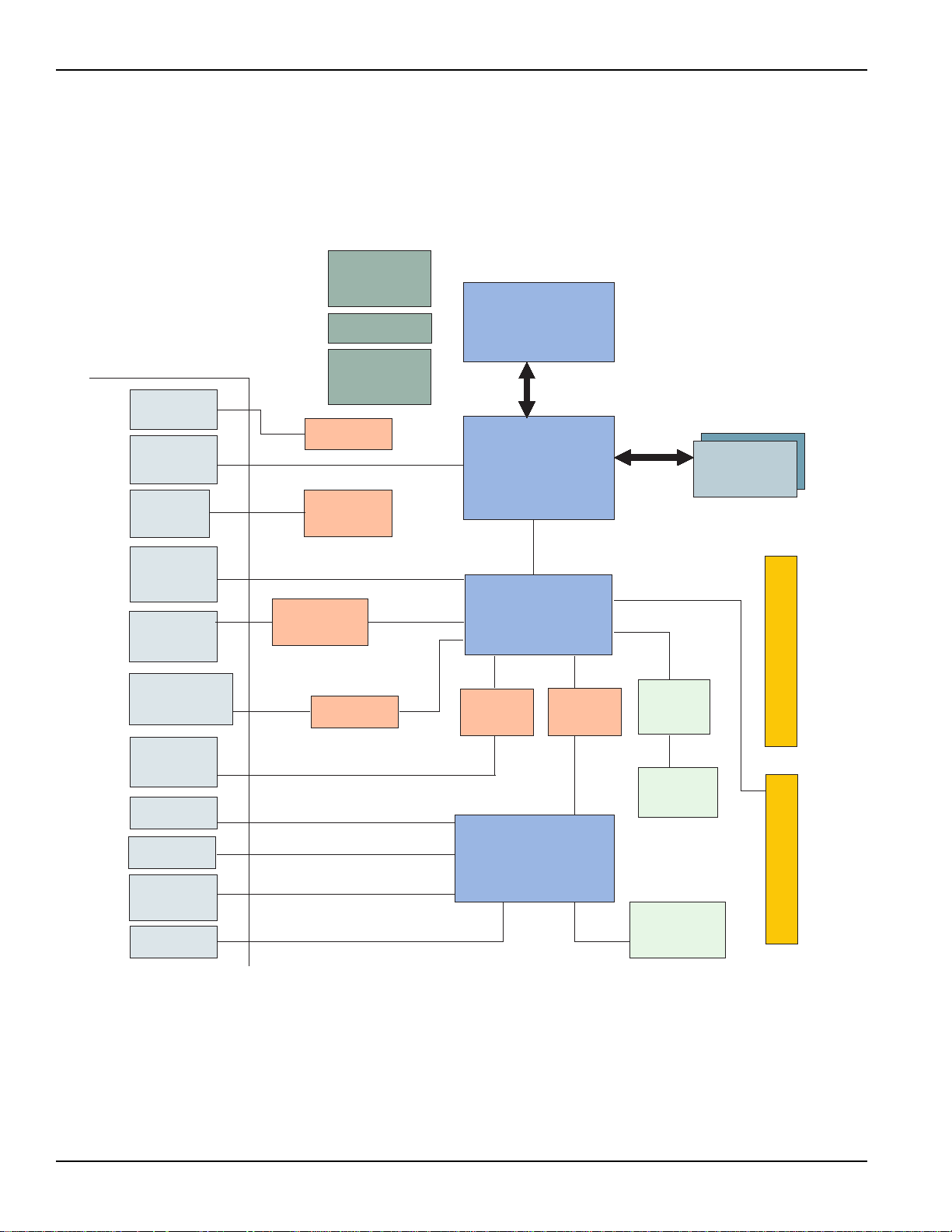
Functional block diagram
The following sections give an overview the Model KPXI-CON controller’s main features as
outlined in the functional block diagram
Figure 1-1
Functional block diagram
Clock
Generator
PWM
Figure 1-1.
Pentium M
or
Celeron
Front Panel (3 Slot)
PXI TRIG
VGA
Reset/
LEDs
USB 2.0
x2
Compact
Flash
GigaLAN
1000/100/10
Audio
Jack
COM1
ASIC
CRT
Reset
Logic
USB2.0 x2
USB -to-CF
controller
PCI -X 64bit/66MHz
LAN
Speaker out
82545EM
HW
monitor
USB2.0
400MHz
Intel 855GME
Hub I/F
1.5
Intel 6300ESB
AC97
Codec
GMCH
ICH
LPC
FWH
BIOS
DDR
200/266
DDR SO -
DDR333
(GME)
PCI 32bit/33MHz
IDE1
CF
socket
IDE
(44pin)
DIMM
Compact PCI J2
Comp act PCI J1
COM2
PS2 KB/MS
LPT
PRN
Winbond
W83627HF
Floppy
(optional)
PXI bus interface
The Model KPXI-CON controller is built on the PICMG 2.8 Instrumentation Extensions to
CompactPCI Specification. PXI specifications dedicate the slot furthest to the left of the PXI
chassis to the System Controller. PXI is electrically compatible with the PCI local bus standard,
and provides enhanced instrumentation signals for synchronization or communication between
peripherals. Based on the mechanical design of CompactPCI systems, PXI systems provide the
1-4 Return to Section Topics KPXI-CON-900-01 Rev. A / January 2007
Page 19

KPXI System Controller User’s Manual Section 1: Introduction
high levels of environmental performance required by the vibration, shock, temperature, and
humidity extremes of industrial environments.
The Model KPXI-CON controller utilizes a 32-bit/33MHz PCI bus and can be used in the
Keithley
As PXI compliant controllers they can be used with any PXI compliant chassis from any
manufacturer.
Instruments PXI chassis listed below:
• KPXI-SYS-6-250, 6-slot 3U PXI Instrument chassis
• KPXI-SYS-8-400, 8-slot 3U PXI Instrument chassis
• KPXI-SYS-14-500, 14-slot 3U PXI instrument chassis
• KPXI-SYS-18-460X2, 18-slot 3U PXI Instrument chassis
CPU support
The KPXI-CON controller supports a single Intel® Pentium® M Processor with 1MB L2 cache in
478-pin Micro-FCPGA or 479-ball Micro-FCBGA package. The standard Model KPXI-CON
controller comes with a CPU socket which can be installed with a Micro-FC-PGA package CPU,
including Pentium M 1.1GHz, 1.6GHz and 1.8GHz. The Pentium M processor runs at a core speed
up to 1.8GHz, with a Front Side Bus (FSB) speed of 400MHz.
The Intel Pentium M processor is a high performance, low power mobile processor with several
micro-architectural enhancements over existing Intel mobile processors. The key features of the
processor are listed as follows:
• Support Intel Architecture with Dynamic Execution
• On-die, primary 32-KB instruction cache and 32-KB write-back data cache
• On-die, 1-MB second level cache with Advanced Transfer Cache Architecture
• Advanced Branch Prediction and Data Prefetch Logic
• Streaming SIMD Extensions 2 (SSE2)
• 400-MHz, Source-Synchronous processor system bus
• Advanced Power Management features including Enhanced Intel SpeedStep® technology
The Pentium M processor runs at a core speed up to 1.8GHz, with a Front Side Bus (FSB) speed
of 400MHz.
Memory support
The Model KPXI-CON controller is based on Intel 855GME chipset, which consists of 855GME
Graphics Memory Controller Hub (GMCH) and the 6300ESB I/O Controller Hub (ICH). The GMCH
system memory interface supports the following features:
• Single channel of x72, unbuffered, ECC DDR SDRAM (SO-DIMM)
• 200, 266MHz and 333MHz DDR device
• 64-bit data interface(72-bit with ECC)
• Up to two double-sided SO-DIMMs (four rows populated) with unbuffered PC2100/PC2700
DDR-SDRAM (with or without ECC)
• Up to 16 simultaneous open pages
• 64MB, 128MB, 256MB, and 512MB technologies for x8 and x16 width devices
• System memory supports up to 2GB
• SDRAM speed, type and size can be determined by the BIOS reading the SO-DIMM
presence detect bits on the System Management Bus (SMBus)
• SDRAM timing register, which provides the DRAM speed control for the entire array, is
programmed to use the timings of the slowest DRAMs installed.
KPXI-CON-900-01 Rev. A / January 2007 Return to Section Topics 1-5
Page 20

Section 1: Introduction KPXI System Controller User’s Manual
Ethernet interfaces
The Model KPXI-CON controller supports an Intel 82545EM Gigabit Ethernet controller. It
integrates MAC and PHY functions into a single chip to provide a standard IEEE 802.3 Ethernet
interface for 10/100/1000BASE-T applications. The controller provides a 64-bit wide interface
compliant with PCI 2.3 and PCI-X 1.0a specifications. The Ethernet interface is routed to an RJ45
port with activity/speed LEDs.
Display interfaces
The Intel® 855GME GMCH chip has dual independent display pipes which can support concurrent
or simultaneous display on each display device. The 350MHz integrated 24bit RAMDAC supports
analog display pixel resolution up to 1600x1200 at 85Hz and 2048x1536 at 75Hz.
Universal Serial Bus (USB)
The Model KPXI-CON controller supports three USB 2.0 serial ports. Ports 1 and 2 are on the front
panel, port 3 is used as a USB-to-CF or USB-to-IDE adaptor to support a Compact Flash Type II
socket on the front panel or a 2.5” IDE HDD. Additional ports can be added through the use of an
external USB hub. USB allows for the easy addition of peripherals such as mouse, keyboard,
speakers, etc. Transfer rates of up to 480Mb/s are supported. High-speed connections require
shielded cables. The Model KPXI-CON controller provides each USB port 0.5A at 5V to power
peripherals and each USB port is protected by a power distribution switch (0.5A rating allows for
inrush currents).
Hot-swappable CF interface
An external CompactFlash socket is available on the Model KPXI-CON controller front panel. The
external CompactFlash interface provides Plug and Play features and is also hot swappable.
Therefore, a CompactFlash card can be used as a replacement for floppy disks and can also
provide very large storage capability (up to 1GB). It is also possible to set this CF interface as a
boot device by selecting boot from USB in the BIOS menu. For information on changing BIOS
settings see
Appendix B. Note that drivers are needed for the external CompactFlash interface.
Serial I/O
The Model KPXI-CON controller provides support for two 16C550 UART compatible COM ports.
COM1 and COM2 are accessible from the front faceplate through DB-9 connectors.
IEEE-1284 parallel port/printer interface
The parallel I/O interface signals are routed to the DB-25 connector on the front faceplate. This
port supports the full IEEE-1284 specification and provides a basic printer interface. The BIOS will
initialize the parallel port as LPT1 with an ISA I/O base address of 378h. This default configuration
also assigns the parallel port to IRQ7. The printer interface mode (Normal, Extended, EPP, or
ECP) is selectable through the BIOS menu. For information on changing BIOS settings see
Appendix B.
PXI trigger I/O port
The Model KPXI-CON System Controller provides one PXI trigger I/O port on the front panel for
advanced PXI trigger functionality. The TRIG I/O is the software-controlled trigger connection for
routing PXI triggers to or from the backplane trigger bus. All trigger lines are compatibility with TTL
1-6 Return to Section Topics KPXI-CON-900-01 Rev. A / January 2007
Page 21

KPXI System Controller User’s Manual Section 1: Introduction
voltage levels and are edge sensitive. Please refer to Figure 1-2 for the detailed block diagram of
PXI Trigger I/O.
Figure 1-2
PXI Trigger I/O block diagram
AC ’97 multimedia audio output
The Model KPXI-CON System Controller supports an AC ‘97 2.2 compliant audio stereo output
with amplifier. Supports multiple sample rates up to 48 kHz.
Hardware monitor function
Two devices provide all the hardware monitor functions of a Model KPXI-CON controller system.
The ADM1032 provides a CPU temperature monitor with programmable over/under temperature
limits and over temperature alarm. The Winbond W83627HF provides system temperature and DC
voltage monitoring.
Table 1-1
W83627HF hardware monitor inputs
83627HF Pin
Name
-12VIN -12V +/- 5%
+12VIN +12V +/- 5%
+3.3VIN +3.3V +/- 5%
VSB +5VSB +/- 5%
VCOREB +1.05V +/- 5%
VCOREA CPU_VCORE Processor core voltage
VTIN1 System Temperature
VTIN2 External Temperature Sensor Input
OVT# CPU over temperature shutdown output
BEEP Beep function for hardware monitor
Voltage/
Temperature
Function/Comments
KPXI-CON-900-01 Rev. A / January 2007 Return to Section Topics 1-7
Page 22

Section 1: Introduction KPXI System Controller User’s Manual
Watchdog Timer
The Model KPXI-CON controller system implements two watchdog timers. The Intel® 6300ESB
provides one 2-stage programmable watchdog timer (WDT) and the W83627HF provides one 1stage programmable watchdog timer.
6300ESB Watchdog Timer
• Supports selectable prescaler – approximately 1MHz (1µs to 1s) and approximately 1KHz
(1ms to 10min).
• The 2-stage WDT mode operates as follows: When the first programmed time expires
before the counter is reloaded, the WDT generates an IRQ, SMI, or SCI interrupt and loads
the second programmed value. If the host still fails to reload the WDT before the second
timeout, the WDT drives WDT_TOUT# low and resets Model KPXI-CON controller system.
W83627HF Watchdog Timer
• Watchdog timer is programmable from 1 to 255 seconds.
• Time out will generate interrupt to NMI or RESET, BIOS selectable.
LED Setting
The Model KPXI-CON System Controller provides four LEDs on the front panel to display the
following information:
• System Active LED: This Green LED will turn on after POST; turn off when system is
• IDE LED: This amber LED flashes when the IDE port is accessed.
• WDT LED: This Red LED should be off in normal situations. The LED flashes after the WDT
• General Purpose LED: This Blue LED is a general purpose LED. Customers can define
Specifications
Refer to the product data sheet for updated Model KPXI-CON System Controller specifications.
Check the Keithley Instruments website at www.keithley.com for the latest updates to the
specifications. See below for general specifications.
PXI/CompactPCI compliancy
• PXI Specification Rev 2.2
• PICMG 2.0 CompactPCI Rev. 3.0
Form factor
powered off.
is enabled by software. The LED turns on steady when the WDT times out.
this LED through software.
• Standard PXI 3U form factor (board size: 100mm x 160mm)
• 3-slot (12 HP) width
CPU/Cache
• Supports Intel® Pentium® M processor, CPU frequency up to 1.8GHz
• Front Side Bus (FSB) frequency: 400MHz
• Cache size: 1MB on-die cache
1-8 Return to Section Topics KPXI-CON-900-01 Rev. A / January 2007
Page 23

KPXI System Controller User’s Manual Section 1: Introduction
Chipset
• Intel® 855GME Graphic Memory Controller Hub (GMCH)
• Intel® 6300ESB I/O Controller Hub
Host memory
• Two 200-pin SO-DIMM sockets for DDR SDRAM, up to 2GB with or w/o ECC
BIOS
• Award PnP BIOS with 4Mb LPC compatible Flash ROM
• BIOS write protection provides anti-virus capability
• DMI BIOS Support: Desktop Management Interface (DMI) allows users to download system
hardware-level information such as CPU type, CPU speed, internal/external frequencies,
and memory size
• For information on changing BIOS settings see Appendix B
CompactPCI bus controller
• PLXtech PCI-6540 Universal PCI-X to PCI-X bridge, supports transparent and nontransparent mode
• PCI-X Rev 1.0 compliant
• Supports 64-bit/66MHz, 64-bit/33MHz, 32-bit/33MHz
Graphics
• Integrated into 855GME GMCH
• 350MHz integrated 24bit RAMDAC supports analog display pixel resolution up to
1600x1200 at 85Hz and 2048x1536 at 75Hz
• Up to 64MB of dynamic video memory allocation
• Dual independent display pipes support concurrent or simultaneous display on each display
device
• Front panel analog VGA DB-15 connector is available
Gigabit ethernet
• Intel® 82545EM Gigabit Ethernet controller provides one 10/100/1000 Mbps Gigabit
Ethernet port via a RJ-45 connector on the front panel.
• Standard IEEE 802.3 Ethernet interface
• 64-bit wide interface compliant with PCI 2.3 and PCI-X 1.0a Specifications
Onboard peripherals
• Integrated into Intel® 6300ESB southbridge
• One EIDE connector supports a 2.5” HDD with Ultra ATA 66/100 support
• Four USB 2.0 ports
– USB 1 and 2 are on the front panel
– USB 3 is used for USB-to-CF to support CompactFlash Type II socket on front panel
• Two CompactFlash Type I/II sockets
– Supports one CompactFlash Type II interface through IDE interface
KPXI-CON-900-01 Rev. A / January 2007 Return to Section Topics 1-9
Page 24

Section 1: Introduction KPXI System Controller User’s Manual
– Supports one CompactFlash Type II drive using USB to CF adaptor
• Supports up to three 16C550 UART compatible COM ports
– COM1 and COM2 are on front faceplate
• One PXI trigger input/output on front panel
• One AC ‘97 2.2 compliant audio stereo output with amplifier on the front panel. Supports
multiple sample rates up to 48KHz.
• One high-speed bi-directional SPP/EPP/ECP parallel port
• PS2 keyboard/mouse combo port on front panel
Front panel LED indicators and reset button
• Four LEDs on the front panel including System Active LED (Green), IDE LED (Amber),
Watchdog timer LED (Red), and General Purpose LED (Blue).
• Flush tact switch for system reset
Real-time clock and nonvolatile memory
The Model KPXI-CON controller system provides a century calendar as well as a time of day
function. In addition, 256 bytes of battery backed-up RAM are available for use by the BIOS. A
separate 3V coin cell battery provides battery backup.
Environment
• Operating temperature: 0°C to 50°C
• Storage temperature: -20°C to 80°C
• Humidity: 5% to 95% RH non-condensing
• Shock: 15G peak-to-peak, 11ms duration, non-operation
• Vibration:
– Non-operation: 1.88Grms, 5-500Hz, each axis
– Operation: 0.5Grms, 5-500Hz, each axis, with 2.5” HDD
Safety Certificate and Test
•CE
• All plastic material, PCB and Battery used are all UL-94V0 certified
Unpacking and inspection
The Model KPXI-CON was carefully inspected electrically and mechanically before shipment. After
unpacking all items from the shipping carton, check for any obvious signs of physical damage that
may have occurred during transit. Report any damage to the shipping agent immediately. Save the
original packing carton for possible future shipment.
1-10 Return to Section Topics KPXI-CON-900-01 Rev. A / January 2007
Page 25
KPXI System Controller User’s Manual Section 1: Introduction
Shipment contents
The following items are included with every Model KPXI-CON series order:
• One of the following models of System Controllers (equipped with CPU, RAM and HDD):
– KPXI-CON-PM-1.8G: 3U PXI system controller with Pentium M 1.8GHz CPU, 512MB
RAM, 40GB HDD
– KPXI-CON-PM-1.8G-PLUS: 3U Pentium M CPU module with Pentium M 1.8GHz CPU,
2GB memory, 80G HDD
– KPXI-CON-CM-1.3G: 3U PXI system controller with Celeron M 1.3GHz CPU, 512MB
RAM, 40GB HDD
• CD containing required software and manuals
• Windows XP CD
• Y-Cable for PS/2 Keyboard and Mouse
CAUTION: This board must be protected from static
discharge and physical shock. Never
touch any of the socketed parts except at
a static-free workstation. Use the antistatic bag shipped with the product to
handle the board. Wear a grounded wrist
strap when touching components.
Inspection for damage
CAUTION: Your Model KPXI-CON controller
The Model KPXI-CON controller was carefully inspected electrically and mechanically before
shipment.
Inspect the controller carton for obvious damages. Shipping and handling may damage the
module. Make sure there are no shipping and handling damages on the controller’s carton before
continuing.
After opening the card module carton, extract the system module and place it only on a grounded
anti-static surface with component side up. Save the original packing carton for possible future
shipment.
Again, inspect the module for damages. Report any damage to the shipping agent immediately.
contains electro-static sensitive
components that can be easily be
damaged by static electricity.
Therefore, handle the controller on a
grounded anti-static mat. The operator
should be wearing an anti-static
wristband, grounded at the same point as
the anti-static mat.
KPXI-CON-900-01 Rev. A / January 2007 Return to Section Topics 1-11
Page 26

Section 1: Introduction KPXI System Controller User’s Manual
Instruction manual
A CD-ROM containing this User’s Manual and required software is included with each Model
KPXI-CON controller order. If a hardcopy of the Model KPXI-CON Series User’s Manual is
required, you can order the Manual Package (Keithley Instruments Part Number
KPXI-CON-900-01). The Manual Package includes an instruction manual and any pertinent
addenda.
Always check the Keithley Instruments’ website at www.keithley.com for the latest revision of the
manual. The latest manual can be downloaded (in PDF format) from the website.
Repacking for shipment
Should it become necessary to return the Model KPXI-CON controller for repair, carefully pack the
unit in its original packing carton or the equivalent, and follow these instructions:
• Call Keithley Instruments’ repair department at 1-888-KEITHLEY (1-888-534-8453) for a
Return Material Authorization (RMA) number.
• Let the repair department know the warranty status of the Model KPXI-CON controller.
• Write ATTENTION REPAIR DEPARTMENT and the RMA number on the shipping label.
• Complete and include the Service Form located at the back of this manual.
Optional accessories
NOTE Check the Keithley Instruments website (www.keithley.com) for additional accessories
that may have been added to the Keithley Instruments product line for the
Model
KPXI-CON System Controller.
• Model 4200-FPD-RM: 1U 17” TFT display with keyboard and pointing device
• Model EM-23B: Keyboard with integrated trackball mouse
• Model KPXI-DIG-CAB-1: 1m (3.3 ft) SMB to SMB cable
• Model KPXI-DIG-CAB-2: 1m (3.3 ft) SMB to BNC converter cable
• Model KPXI-USB-CD: External USB CD drive for controllers
1-12 Return to Section Topics KPXI-CON-900-01 Rev. A / January 2007
Page 27

In this section:
Topic Page
Introduction......................................................................................... 2-2
Peripheral connectivity .................................................................... 2-2
Model KPXI-CON controller I/O connectors ............................... 2-3
Model KPXI-CON controller connector pin assignments ....... 2-3
Section 2
I/O Connectors and Pin Assignment
Model KPXI-CON controller front panel I/O connectors ................... 2-3
PXI trigger connector........................................................................ 2-3
VGA connector ................................................................................. 2-4
USB port 1, 2 connector ................................................................... 2-4
Ethernet (RJ-45) connector .............................................................. 2-5
COM1, 2 serial port connector DB-9 ................................................ 2-5
LPT printer port connector DB-25..................................................... 2-6
General purpose LED definitions...................................................... 2-7
CompactFlash type I/II connector..................................................... 2-7
PS/2 keyboard/mouse combo connector (mini DIN-6) ..................... 2-8
J1 connector pin assignment............................................................ 2-8
J2 connector pin assignment............................................................ 2-9
Page 28

Section 2: I/O Connectors and Pin Assignment KPXI System Controller User’s Manual
Introduction
This section provides information about the board outline and connector definitions to allow users
to become familiar with the Model KPXI-CON controller before use. Included are the following
topics:
• Model KPXI-CON controller peripheral connectivity
• Model KPXI-CON controller I/O connectors
• Model KPXI-CON controller connector pin assignments
Peripheral connectivity
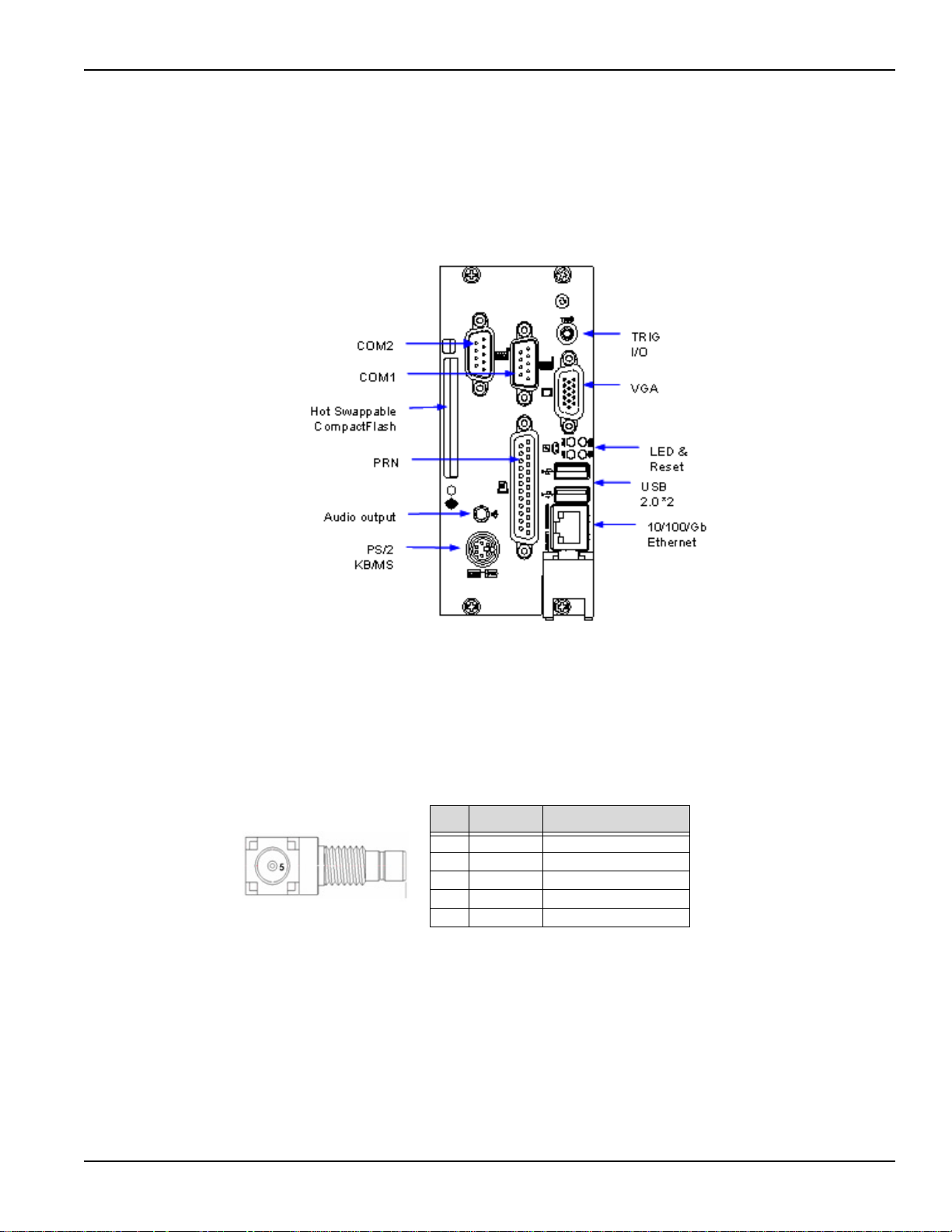
Table 2-1 lists the peripherals and their corresponding Model KPXI-CON controller connectors.
Table 2-1
Peripheral connectivity table
Peripheral External Connector
Video VGA (DB-15)
Serial Port COM1 (DB-9)
Serial Port COM2 (DB-9)
Parallel Port PRN (DB-25)
PXI trigger TRIG (SMB)
Keyboard/Mouse PS/2 (Mini DIN-6)
CompactFlash CF2 Socket (Supported by
USB-to-CF adaptor)
USB 2.0 Port USB 1,2 (USB 4-pin series)
Gigabit Ethernet LAN (RJ-45)
Audio speaker output
LEDs Y
Reset button Y
Y
2-2 Return to Section Topics KPXI-CON-900-01 Rev. A / January 2007
Page 29
KPXI System Controller User’s Manual Section 2: I/O Connectors and Pin Assignment
Model KPXI-CON controller I/O connectors
Model KPXI-CON controller front panel I/O connectors
Figure 2-1
Model KPXI-CON controller front panel I/O connectors
Model KPXI-CON controller connector pin assignments
PXI trigger connector
Table 2-2
PXI trigger connector pin assignment
Pin Signal Function
1 GND Ground
2 GND Ground
3 GND Ground
4 GND Ground
5 PXI_TRG PXI trigger signal
KPXI-CON-900-01 Rev. A / January 2007 Return to Section Topics 2-3
Page 30

Section 2: I/O Connectors and Pin Assignment KPXI System Controller User’s Manual
VGA connector
Table 2-3
VGA connector pin assignment
Pin Signal Function
1 RED Analog RED
2 GREEN Analog GREEN
3 BLUE Analog BLUE
4 NC No Connect
5 GND Ground
6 GND Ground
7 GND Ground
8 GND Ground
9 +5V Power In
10 GND Ground
11 NC No Connect
12 DDCDAT DDC Data for CRT
13 HSYNC Horizontal sync for Monitor
14 VSYNC Vertical sync for Monitor
15 DDCCLK DDC CLK for CRT
USB port 1, 2 connector
Table 2-4
USB connector pin assignment
Pin Signal Function
1 USBVCC Power
2 USB- Data (-)
3 USB+ Data (+)
4 USBGND Ground
2-4 Return to Section Topics KPXI-CON-900-01 Rev. A / January 2007
Page 31

KPXI System Controller User’s Manual Section 2: I/O Connectors and Pin Assignment
Ethernet (RJ-45) connector
Table 2-5
Ethernet connector pin assignment
Pin Signal Function
1 TDP Transmit Data (+)
2 TDN Transmit Data (-)
3 RDP Receive Data (+)
4 LANCT1 Termination
5 LANCT2 Termination
6 RDN Receive Data (-)
7 NC No Connect
8 GND Ground
9 TDP Transmit Data (+)
Table 2-6
Ethernet LED status definitions
Status Yellow LED Green LED
Network link is not established OFF OFF
10 Mbps(10 BaseT) Link ON OFF
Active Flash OFF
100 Mbps (100 BaseT) Link ON OFF
Active Flash OFF
1000 Mbps (1000 BaseT) Link ON ON
Active Flash ON
COM1, 2 serial port connector DB-9
Table 2-7
COM connector pin assignment
Pin Signal Function
1 DCD# Data Carrier Detect
2 RXD Receive Data
3 TXD Transmit Data
4 DTR# Data Terminal Ready
5 GND Ground
6 DSR# Data Set Ready
7 RTS# Request to Send
8 CTS# Clear to Send
9 RI# Ring Indicate
KPXI-CON-900-01 Rev. A / January 2007 Return to Section Topics 2-5
Page 32

Section 2: I/O Connectors and Pin Assignment KPXI System Controller User’s Manual
LPT printer port connector DB-25
Table 2-8
LPT printer port connector DB-25
Signal Name Pin Pin Signal Name
Line printer strobe 1 14 AutoFeed
PD0, parallel data 0 2 15 Error
PD1, parallel data 1 3 16 Initialize
PD2, parallel data 2 4 17 Select In
PD3, parallel data 3 5 18 Ground
PD4, parallel data 4 6 19 Ground
PD5, parallel data 5 7 20 Ground
PD6, parallel data 6 8 21 Ground
PD7, parallel data
7
ACK, acknowledge 10 23 Ground
Busy 11 24 Ground
Paper empty 12 25 Ground
Select 13
9 22 Ground
2-6 Return to Section Topics KPXI-CON-900-01 Rev. A / January 2007
Page 33

KPXI System Controller User’s Manual Section 2: I/O Connectors and Pin Assignment
General purpose LED definitions
Table 2-9
General purpose LED definitions
LED Color Status Description
System Active
(PW)
IDE (HD) Yel lo w OFF IDE idle
WDT (WD) Red OFF WDT not enabled
General
Purpose (GP)
Green OFF System power not on or power failure
ON Power ON
Flash IDE access
Flash WDT enabled
ON WDT timeout occur
Blue OFF Controller installed and active
ON Controller installed but not active
CompactFlash type I/II connector
Table 2-10
CompactFlash connector pin assignment
Signal Name Pin Pin Signal Name
GND 1 26 GND
SDD3 2 27 SDD11
SDD4 3 28 SDD12
SDD5 4 29 SDD13
SDD6 5 30 SDD14
SDD7 6 31 SDD15
SDCS#1 7 32 SDCS#3
GND 8 33 GND
GND 9 34 SDIOR#
GND 10 35 SDIOW#
GND 11 36 +5V
GND 12 37 IDEIRQ14
+5V 13 38 +5V
GND 14 39 PCSEL
GND 15 40 NC
GND 16 41 SIDERST#
GND 17 42 SIORDY
SDA2 18 43 NC
SDA1 19 44 SDDACK#
SDA0 20 45 IDEACT#
SDD0 21 46 S66DECT
SDD1 22 47 SDD8
SDD2 23 48 SDD9
IOIS16# 24 49 SDD10
GND 25 50 GND
KPXI-CON-900-01 Rev. A / January 2007 Return to Section Topics 2-7
Page 34

Section 2: I/O Connectors and Pin Assignment KPXI System Controller User’s Manual
PS/2 keyboard/mouse combo connector (mini DIN-6)
Table 2-11
PS/2 connector pin assignment
Pin Signal Function
1 KBDATA Keyboard Data
2 MSDATA Mouse Data
3 GND Ground
4 VCC Power
5 KBCLK Keyboard Clock
6 MSCLK Mouse Clock
J1 connector pin assignment
Table 2-12
J1 connector pin assignment
Pin Z A B C D E F
J1-25 GND +5V REQ64# ENUM# +3.3V +5V GND
J1-24 GND AD[1] +5V V(I/O) AD[0] ACK64# GND
J1-23 GND +3.3V AD[4] AD[3] +5V AD[2] GND
J1-22 GND AD[7] GND +3.3V AD[6] AD[5] GND
J1-21 GND +3.3V AD[9] AD[8] M66EN C/BE[0]# GND
J1-20 GND AD[12] GND V(I/O) AD[11] AD[10] GND
J1-19 GND +3.3V AD[15] AD[14] GND AD[13] GND
J1-18 GND SERR# GND +3.3V PAR C/BE[1]# GND
J1-17 GND +3.3V NC NC GND PERR# GND
J1-16 GND DEVSEL# GND V(I/O) STOP# LOCK# GND
J1-15 GND +3.3V FRAME# IRDY# GND TRDY# GND
J1-12~14 Keying Area
J1-11 GND AD[18] AD[17] AD[16] GND C/BE[2]# GND
J1-10 GND AD[21] GND +3.3V AD[20] AD[19] GND
J1-9 GND C/BE[3]# GND AD[23] GND AD[22] GND
J1-8 GND AD[26] GND V(I/O) AD[25] AD[24] GND
J1-7 GND AD[30] AD[29] AD[28] GND AD[27] GND
J1-6 GND REQ0# GND +3.3V CLK0 AD[31] GND
J1-5 GND NC NC RST# GND GNT0# GND
J1-4 GND NC HEALTHY# V(I/O) INTP INTS GND
J1-3 GND INTA# INTB# INTC# +5V INTD# GND
J1-2 GND TCK +5V TMS TDO TDI GND
J1-1 GND +5V -12V TRST# +12V +5V GND
Pin Z A B C D E F
2-8 Return to Section Topics KPXI-CON-900-01 Rev. A / January 2007
Page 35

KPXI System Controller User’s Manual Section 2: I/O Connectors and Pin Assignment
J2 connector pin assignment
Table 2-13
J2 connector pin assignment
Pin Z A B C D E F
J2-22 GND NC NC NC NC NC GND
J2-21 GND CLK6 GND NC RSV RSV# GND
J2-20 GND CLK5 GND RSV GND RSV GND
J2-19 GND GND GND SMB_SDA SMB_SCL SMB_ALERT# GND
J2-18 GND PXI_TRIG3 PXI_TRIG4 PXI_TRIG5 GND PXI_TRIG6 GND
J2-17 GND PXI_TRIG2 GND REST# REQ6# GNT6# GND
J2-16 GND PXI_TRIG1 PXI_TRIG0 DEG# GND PXI_TRIG7 GND
J2-15 GND NC GND FA L# REQ5# GNT5# GND
J2-14 GND AD[35] AD[34] AD[33] GND AD[32] GND
J2-13 GND AD[38] GND V(I/O) AD[37] AD[36] GND
J2-12 GND AD[42] AD[41] AD[40] GND AD[39] GND
J2-11 GND AD[45] GND V(I/O) AD[44] AD[43] GND
J2-10 GND AD[49] AD[48] AD[47] GND AD[46] GND
J2-9 GND AD[52] GND V(I/O) AD[51] AD[50] GND
J2-8 GND AD[56] AD[55] AD[54] GND AD[53] GND
J2-7 GND AD[59] GND V(I/O) AD[58] AD[57] GND
J2-6 GND AD[63] AD[62] AD[61] GND AD[60] GND
J2-5 GND C/BE[5] GND V(I/O) C/BE[4]# PA R 6 4 GND
J2-4 GND V(I/O) NC C/BE[7]# GND C/BE[6]# GND
J2-3 GND CLK4 GND GNT3# REQ4# GNT4# GND
J2-2 GND CLK2 CLK3 SYSEN# GNT2# REQ3# GND
J2-1 GND CLK1 GND REQ1# GNT1# REQ2# GND
Pin Z A B C D E F
KPXI-CON-900-01 Rev. A / January 2007 Return to Section Topics 2-9
Page 36

Section 2: I/O Connectors and Pin Assignment KPXI System Controller User’s Manual
This page left blank intentionally.
2-10 Return to Section Topics KPXI-CON-900-01 Rev. A / January 2007
Page 37

In this section:
Top ic Pa ge
Introduction......................................................................................... 3-2
Installing the Model KPXI-CON controller................................... 3-2
BIOS configuration overview ......................................................... 3-2
BIOS configuration overview ......................................................... 3-2
Operating system installation........................................................ 3-3
Section 3
Getting Started
How to remove the controller from the PXI chassis.......................... 3-2
Page 38

Section 3: Getting Started KPXI System Controller User’s Manual
Introduction
This section gives a summary of what is required to set up an operating system using the Model
KPXI-CON controller. Hardware installation and BIOS setup are also discussed. Note that the
Model KPXI-CON controller is shipped with CPU, RAM, HDD, and Windows XP
system preinstalled.
®
operating
Installing the Model KPXI-CON controller
Use the following procedure to install the Model KPXI-CON controller into a PXI chassis. Consult
your PXI chassis user guide for specific instructions and warnings.
Step 1: Plug in your chassis before installing the Model KPXI-CON controller. Make sure the
system power is turned off.
Step 2: Remove the blank face panel from the system slot.
Step 3: Align the top and bottom edges of the board with the card guides on the chassis, then slide
the board into the chassis until resistance is felt.
Step 4: Move the locking handle in an inward direction until it is fully latched. Please note that
slight resistance will be felt while inserting the board. If this resistance is more than under
normal conditions, check to ensure that there are no bent pins on the backplane and that
the board’s connector pins are aligned properly with the connectors on the backplane.
Step 5: Verify that the board is seated properly. Secure the four screws at the top and bottom of
the front panel; connect the appropriate cables to the board. The system can now be
powered on.
Figure 3-1 shows a Model KPXI-CON controller being installed in the system slot of a typical
Keithley Instruments chassis.
How to remove the controller from the PXI chassis
Step 1: Power off the chassis.
Step 2: Loosen the four screws in the front panel.
Step 3: Press down on the red locking tab on the ejector handle then press down on the ejector
handle itself which will eject the controller from its seated position.
Step 4: Slide the controller out of the chassis.
CompactFlash card installation
The CompactFlash Card (or CF storage card) is widely used in digital consumer devices like
PDAs, digital cameras, and MP3 players. The CF format features anti-shock and anti-vibration
properties, improved environmental tolerance, low power consumption, a small form factor, and
higher reliability. Plus, it has been widely accepted in the industrial and embedded application
field.
The Model KPXI-CON controller has an external CompactFlash socket. The external CF interface
is hot swappable so users can install or remove via the front panel while the system is running.
BIOS configuration overview
The Basic Input/Output System (BIOS) is a program that provides the basic level of
communication between the processor and peripherals. In addition, the BIOS also contain code for
various advanced features found in the system board. The BIOS setup program includes menus
3-2 Return to Section Topics KPXI-CON-900-01 Rev. A / January 2007
Page 39

KPXI System Controller User’s Manual Section 3: Getting Started
for configuring settings and enabling Model KPXI-CON controller controller features. Most users
do not need to use the BIOS setup program, as the Model KPXI-CON controller controller ships
with default settings that work well for most configurations. Please refer to the BIOS Manual (see
Appendix B) for detailed information about the BIOS and other utilities.
CAUTION:
Changing BIOS settings may lead to incorrect controller
behavior and possibly an unbootable controller. In general, do
not change a BIOS setting unless you are absolutely certain of
what it does.
Figure 3-1
Model KPXI-CON System Controller installation in PXI Chassis
Typical PXI
chassis
Front panel
screws
Card guide
Operating system installation
Keithley PXI System Controllers come pre-installed with a Windows XP Operating System. In
some cases reinstallation of Windows XP may be necessary or desirable. For this purpose the
original Windows XP CD is shipped with each controller. You may wish to install an operating
system not supported by Keithley Instruments. In that case, refer to the documentation provided by
the operating system vendor.
Read the release notes and installation documentation provided by the operating system vendor.
Be sure to read all the README files or documents provided on the distribution disks, as these
typically note documentation discrepancies or compatibility problems.
To reinstall the operating system use the KPXI-USBCD external USB CDROM drive. The BIOS is
by default set to boot from the USB CDROM when connected with bootable media. For information
on changing the boot sequence see
Controllers edge
Ejector latch
Appendix B.
KPXI-CON-900-01 Rev. A / January 2007 Return to Section Topics 3-3
Page 40

Section 3: Getting Started KPXI System Controller User’s Manual
This page left blank intentionally.
3-4 Return to Section Topics KPXI-CON-900-01 Rev. A / January 2007
Page 41

In this section:
Top ic Pa ge
Introduction......................................................................................... 4-2
Chipset driver installation ............................................................... 4-2
VGA driver installation ..................................................................... 4-3
LAN driver installation ..................................................................... 4-3
Audio codec driver installation...................................................... 4-4
PXI trigger driver installation ......................................................... 4-4
Section 4
Driver Installation
Installing hardware configuration file ................................................ 4-3
Troubleshooting VGA driver installation ........................................... 4-3
Page 42

Section 4: Driver Installation KPXI System Controller User’s Manual
Introduction
The controller comes preloaded with all KPXI series drivers as well as the Windows XP® drivers
for all the internal hardware components. This section includes instructions for re-installing the
device drivers if Windows had to be reinstalled or device drivers were lost for some other reason.
The driver installation instructions for Windows
To install Windows drivers:
Step 1: Fully install Windows properly before installing any drivers. Most of the standard I/O device
drivers have been included in Windows.
Step 2: Install the chipset driver.
Step 3: Install the VGA driver.
Step 4: Install the LAN driver.
Step 5: Install the Audio driver.
Step 6: Install the PXI Trigger driver.
To ensure compatibility, it is recommended that the chipset, VGA, LAN, Audio, and PXI Trigger
drivers provided in the Keithley Instruments CD are used.
®
XP/2000 are described below.
To install the Windows drivers for the Model KPXI-CON system controller, refer to the installation
information in this section. The Windows drivers are located in the following directories of the
Keithley Instruments CD (
Table 4-1
Windows drivers file locations
Chipset driver \Driver Installation\PXI controller\chipset\Win2KXP
VGA driver \Driver Installation\PXI controller\VGA\
LAN driver \Driver Installation\PXI controller\LAN\
Audio driver \Driver Installation\PXI controller\Audio\
PXI Trigger driver \Driver Installation\PXI controller\PXI_Trigger\
The Bus-mastering IDE drivers are automatically installed by Windows.
For using USB 2.0, please update to the newest Windows Service Pack.
Table 4-1):
Chipset driver installation
This section describes the system requirements of Intel® 855GME chipset device drivers. The
drivers are designed for and tested with Windows XP/2000. The system must contain a supported
Intel processor and chipset configuration. Ensure that a mouse is connected to the system. One of
the following versions of Windows XP/2000 must be installed on the system prior to running the
utility program.
• Windows XP Version 2002 (Original release)
• Windows 2000 5.00.2195 (Original release)
4-2 Return to Section Topics KPXI-CON-900-01 Rev. A / January 2007
Page 43

KPXI System Controller User’s Manual Section 4: Driver Installation
Installing hardware configuration file
Follow the instructions below to install the hardware configuration file on a Windows XP/2000
system.
NOTE Record the location of the Windows XP/2000 directory before installing the drivers.
Step 1: Check the System Requirements. Windows XP/2000 must be fully installed and running
on the system prior to running this software.
Step 2: Close any running applications.
Step 3: The files are stored in an integrated Windows XP/2000 application setup program.
Step 4: Insert the Keithley Instruments CD, run the infinst_enu.exe file at
X:\Driver Installation
Step 5: Click Next on the Welcome Screen to read and agree to the license agreement. Click Yes
if you agree to continue. NOTE: If you click No, the program will terminate.
Step 6: Click Next on the Readme Information screen to install INF files.
Step 7: Click Finish to restart the system when prompted.
Step 8: Follow the screen instructions and use default settings to complete setup when Windows
XP/2000 restarts. Upon restart, Windows may display a dialog box announcing new
hardware has been found and installs drivers for them. If a New Hardware Found dialog
box is displayed requesting the location of the drivers, click on the scrollbar and select the
Windows directory.
\PXI controller\chipset\Win2kXP\ (where X is the CD-ROM drive).
Step 9: Select Yes, when prompted to restart Windows.
VGA driver installation
This section describes the VGA driver installation for the onboard VGA controller Intel® 855E
GMCH2. The relative drivers are located in X:\Driver Installation\PXI Platform\
of the Keithley Instruments CD, where X: is the drive letter of the CD-ROM drive.
Windows 2000 and Windows XP may try to install the standard VGA driver. To ensure
compatibility, manually install the latest driver, which is included in the Keithley Instruments CD. To
update to the new driver, follow the steps below:
Step 1: Boot Windows and execute the win2k_xp149.exe file under this directory:
X:\Driver Installation
Step 2: Follow the prompts. The VGA driver will automatically be installed onto the system.
Step 3: Restart the system.
Troubleshooting VGA driver installation
After installing the VGA/AGP drivers in Windows, it is possible to find the drivers not working
correctly. This may be caused by failing to install the Windows service pack beforehand. Ensure
that the Windows service pack is installed to enable AGP capability.
\PXI controller\VGA\
\PXI controller\VGA\Win2kXP
LAN driver installation
This section describes the LAN driver installation for the onboard Intel® 82545EM Gigabit Ethernet
controller. The drivers included in the Keithley Instruments CD support Windows XP/2000.
KPXI-CON-900-01 Rev. A / January 2007 Return to Section Topics 4-3
Page 44

Section 4: Driver Installation KPXI System Controller User’s Manual
Windows XP/2000 will attempt to install a LAN driver automatically. To ensure compatibility,
manually install the latest LAN driver, which is stored on the Keithley Instruments CD. After
installing Windows XP/2000, update to the new driver by following these procedures:
Step 1: Boot Windows and execute the pro2kxp.exe file under the directory:
X:\Driver Installation\PXI controller\LAN\Win2kXP\
Step 2: Following prompt instructions, The LAN driver will automatically be installed on the
system.
Step 3: Restart the system.
Audio codec driver installation
This section outlines the Audio Codec driver installation for the onboard AC97’ Codec. The drivers
included on the Keithley Instruments CD support Windows XP/2000. Follow the instructions below
to install the Audio driver for Windows XP/2000.
Step 1: Execute the wdm_a365.exe file in the following path location:
X:\Driver Installation\PXI controller\Audio\Win2kXP\
Step 2: Click Next on the Welcome audio setup screen to install driver.
Step 3: Finally, click Finish to restart.
PXI trigger driver installation
This section outlines the PXI Trigger driver installation. The driver included on the Keithley
Instruments CD supports Windows XP/2000. To install the driver for PXI Trigger, follow the
instructions below:
Step 1: Execute the setup.exe file in the following path location:
X:\Driver Installation\PXI controller\PXI_Trigger\Win2k\
Step 2: Click Next on the Welcome PXI Trigger setup screen to install the driver.
Step 3: Finally, click Finish to restart.
4-4 Return to Section Topics KPXI-CON-900-01 Rev. A / January 2007
Page 45

In this section:
Top ic Pa ge
Introduction......................................................................................... 5-2
Section 5
Utilities
Watchdog timer overview................................................................ 5-2
®
Intel
6300ESB ICH watchdog timer ................................................ 5-2
Configuration registers ..................................................................... 5-3
GPIO control registers ...................................................................... 5-4
WDT programming procedure .......................................................... 5-4
W83627HF (Super IO) watchdog timer ............................................ 5-4
Page 46

Section 5: Utilities KPXI System Controller User’s Manual
Introduction
This section explains extended function of the Model KPXI-CON controller (watchdog timer WDT).
Watchdog timer overview
The Model KPXI-CON controller has two different type watchdog timers (WDT), one is integrated
into the south bridge 6300ESB and another is integrated into the super I/O W83627HF. The
primary function of the WDT is to monitor the Model KPXI-CON controller operation and to
generate IRQs and send a signal to PXI Trigger or reset the system if the software fails to function
as programmed. The major features of the watchdog timer are:
1. Enabled and disabled through software control
2. Armed and strobed through software control
Intel® 6300ESB ICH watchdog timer
The Intel® 6300ESB ICH includes a two-stage Watchdog Timer (WDT) that provides a resolution
ranging from one micro second to ten minutes. The timer uses a 35-bit Down-Counter. The
counter is loaded with the value from the first Preload register. The timer is then enabled and starts
counting down. The time at which the WDT first starts counting down is called the first state. If the
host fails to reload the WDT before the 35-bit down counter reaches zero the WDT generates an
internal interrupt. After the interrupt is generated, the WDT loads the value from the second
Preload register into the WDT’s 35-bit Down-Counter and starts counting down. The WDT is now
in the second stage. If the host still fails to reload the WDT before the second timeout, the WDT
drives the WDT_TOUT# pin low. The WDT_TOUT# pin is held low until the system is reset. Users
can choose to reset the system or send a PXI Trigger signal through BIOS WDT setting.
Figure 5-1
Intel® 6300ESB Watchdog Timer architecture
5-2 Return to Section Topics KPXI-CON-900-01 Rev. A / January 2007
Page 47

KPXI System Controller User’s Manual Section 5: Utilities
Configuration registers
The Intel® 6300ESB WDT appears to BIOS as PCI Bus -0, Device 29, Function 4, and has the
standard set of PCI configuration registers. The configuration registers are described below.
Offset 10H: Base Address Register (BAR)
This register determines the memory base for WDT down-counter setting. It will be used to set
Preload value 1 register, Preload value 2 register, General Interrupt Status register and Reload
register.
Preload Value 1 and 2 registers
These two registers are used to hold the preload value for the WDT timer. Its value will be
automatically transferred into the down-counter every time the WDT enters the first stage and
second stage. Preload Value 1 register locates at Base + 00H and Preload Value 2 register locates
at Base + 04H. Only bit [19:0] can be set.
The register unlocking sequence is necessary when writing to the Preload registers. The
procedure of writing a value into preload value 1 and 2 register is as follows:
1. Write 80H to offset BAR + 0CH.
2. Write 86H to offset BAR + 0CH.
3. Write desired value to preload register. (BAR + 00H or BAR + 04H)
General Interrupt Status Register
This register is at Base + 08H. Bit 0 is set when the first stage of down-counter reaches zero.
Bit 0 = 0 – No Interrupt
Bit 1 = 1 – Interrupt Active
Reload Register
This register is at Base + 0CH. Write 1 to bit 8 will reload the down-counter’s value. Instructions on
preventing a timeout is as follows:
1. Write 80H to offset BAR + 0CH.
2. Write 86H to offset BAR + 0CH.
3. Write a ‘1’ to RELOAD[8] of the reload register.
Offset 60 – 61H: WDT Configuration Register
Bit 5 indicates whether or not the WDT will toggle the WDT_TOUT# pin when WDT times out.
(0=Enabled, 1=Disabled)
Bit 2 provides two options for prescaling the main down-counter. (0=1ms – 10min, 1=1us—1sec)
Bit [1:0] allows the user to choose the type of interrupt when the WDT reaches the end of the first
stage without being reset. (00 = IRQ, 01 = reserved, 10 = SMI, 11 = Disabled)
NOTE At present, the WDT does not support SMI. IRQ uses APIC 1, INT 10 and it is active low,
level triggered.
Offset 68H: WDT Lock Register
Bit 1 enables or disables the WDT. (0 = Disabled, 1 = Enabled)
Bit 0 will lock the values of this register until a hard reset occurs or power is cycled. (0 = unlocked,
1 = locked) The default is Unlocked.
KPXI-CON-900-01 Rev. A / January 2007 Return to Section Topics 5-3
Page 48

Section 5: Utilities KPXI System Controller User’s Manual
GPIO control registers
There are three GPIOs on the Model KPXI-CON controller related to the watchdog timer. They are
listed as follows. The GPIO control base port is 480H.
WDT_TOUT# pin selection
The WDT_TOUT# signal is multiplexed with GPIO32. When using WDT, this signal must be
switched to WDT_TOUT# function. It uses bit 0 of GPIOBASE + 30H to set WDT_TOUT function.
(0 = WDT_TOUT#, 1 = GPIO32)
RESET hardware circuit selection
GPO24 of the 6300ESB is designed to control the reset circuit. When GPO24 is low, the system
will reset according to the level of the WDT_TOUT# signal. When GPO24 is high, the system will
not be reset by WDT_TOUT#. Set bit 24 of GPIOBASE + 04H to 0 for output use. Bit 24 of
GPIOBASE + 0CH determines the level of GPO24 (0 = Low, 1 = High). A setting already exists in
the BIOS setup menu. The user can set this item before programming WDT. For information on
changing BIOS settings see
WDT LED Control
GPO25 of the 6300ESB is designed to control WDT LED. Two features of the WDT LED are
supported on Model KPXI-CON controller. WDT LED lights or blinks.
Appendix B.
WDT LED lights: Set bit 25 of GPIOBASE + 04H to 0. Bit 24 of GPIOBASE + 0CH determines the
state of WDT LED. (0 = light, 1= dark)
WDT LED blinks: Set bit 25 of GPIOBASE + 04H to 0. Bit 25 of GPIOBASE + 18H enables WDT
LED blinking function. (0 = function normally, 1 = enable blinking) The high and low times have
approximately 0.5 seconds each.
WDT programming procedure
Step 1: Set BIOS Setting in Integrated Peripherals\Onboard Device Page Watch Dog Timer Item
to Enabled.
Step 2: Make sure WDT_TOUT# signal is functional (not GPIO32 function).
Step 3: Set WDT output enable, presecaler and interrupt type into WDT configuration register.
Step 4: Obtain control base from Base Address register.
Step 5: Program Preload register’s value according to unlocking sequence.
Step 6: Set WDT timer mode into WDT Lock Register.
Step 7: Enable WDT from WDT Lock register and program the functionality of WDT LED.
Step 8: To prevent the timer from causing an interrupt or driving WDT_TOUT#, the timer must be
reloaded periodically. The frequency of reloads required is dependent on the value of the
preload values. To reload the down-counter, the register unlocking sequence must be
performed.
Step 9: If the user wishes to disable WDT, set bit 1 of WDT lock Register to 0.
W83627HF (Super IO) watchdog timer
The W83627HF watchdog timer circuit is implemented in a programmable logic device. The
watchdog timer contains a "Control and Status Register." The register allows the BIOS or user
application to determine if a watchdog time out was the source of a particular reset. The timeout
5-4 Return to Section Topics KPXI-CON-900-01 Rev. A / January 2007
Page 49

KPXI System Controller User’s Manual Section 5: Utilities
period is 1-255 seconds. The watchdog is normally strobed by reading the Watchdog Register
(3F0h). IF the host fails to reload the WDT before the timeout, the WDT drives the WDT_TOUT#
pin low. Users can choose to reset the system or send a PXI Trigger signal through BIOS WDT
setting.
Figure 5-2
W83267HF Watchdog Timer architecture
KPXI-CON-900-01 Rev. A / January 2007 Return to Section Topics 5-5
Page 50

Section 5: Utilities KPXI System Controller User’s Manual
This page left blank intentionally.
5-6 Return to Section Topics KPXI-CON-900-01 Rev. A / January 2007
Page 51

In this appendix:
Top ic Page
Introduction......................................................................................... A-2
Data Types ........................................................................................... A-2
Function Reference...........................................................................A-2
KPXITRIG_Close.............................................................................. A-2
KPXITRIG_GetGPIOBase................................................................ A-3
KPXITRIG_Init ..................................................................................A-3
KPXITRIG_SetSoftTrg...................................................................... A-4
KPXITRIG_Trigger_Clear ................................................................. A-4
KPXITRIG_Trigger_Route................................................................ A-4
Appendix A
KPXI Trigger Function Description
Page 52

Appendix A: KPXI Trigger Function Description KPXI System Controller User’s Manual
Introduction
This appendix provides a description of PXI Trigger functions, including data types and function
reference.
Data Types
We have defined some data types in the Model KPXI-CON controller header file. This header file
can be found in KPXITRIG.H under the directory X:\KEITHLEY\KPXITRIG\Include after running
the setup.exe file (where X is the drive from which you installed the driver). These data types are
used by the Model KPXI-CON controller Library. It is recommended that you use these data types
in your application programs. The following table lists the data type names, their ranges, and the
corresponding data types in C/C++, and Visual Basic.
Tab l e A - 1
Data Types
Type
Name
Description Range
U8 8-bit ASCII
character
I16 16-bit signed
integer
U16 16-bit
unsigned
integer
I32 32-bit signed
integer
U32 32-bit
unsigned
integer
F32 32-bit single-
precision
floating-point
F64 64-bit double-
precision
floating-point
Type
C/C++ ( for 32-
bit compiler)
0 to 255 Unsigned char Byte
-32768 to 32767 Short Integer
0 to 65535 Unsigned short Not supported by
-2147483648 to 2147483647 Long Long
0 to 4294967295 Unsigned long Not supported by
-3.402823E38 to
3.402823E38
-1.797683134862315E308
to
1.797683134862315E309
Float Single
Double Double
Visual Basic
BASIC, use the
signed integer
(I16) instead
BASIC, use the
signed long
integer (I32)
instead
Function Reference
KPXITRIG_Close
Description This function is used to tell the Model KPXI-CON controller library that a regis-
tered card is not currently used and can be released, making room for the new
card to register. At the end of a program, use this function to release all cards that
were registered.
Cards Supported: KPXI Series
Syntax Microsoft C/C++ and Borland C++
I16 KPXITRIG_Close (U16 CardNumber)
A-2 Return to Section Topics KPXI-CON-900-01 Rev. A / January 2007
Page 53

KPXI System Controller User’s Manual Appendix A: KPXI Trigger Function Description
Visual Basic
KPXITRIG_Close (ByVal CardNumber As Integer) As Integer
Parameters CardNumber: The card ID of the card that want to be released.
Return Value NoError
KPXITRIG_GetGPIOBase
Description Get the GPIO base address of the Model KPXI-CON controller.
Cards Supported: KPXI Series
Syntax Microsoft C/C++ and Borland C++
I16 KPXITRIG_GetGPIOBase(U16 wCardNumber, U32 *BaseAddr)
Visual Basic
KPXITRIG_GetGPIOBase (ByVal CardNumber As Integer, BaseAddr
As Long) As Integer
Parameters CardNumber: The card ID of the card to retrieve the DPIO address.
Base Addr: Returns the GPIO base address.
Return Value NoError
KPXITRIG_Init
Description Initializes the hardware and software states of a Model KPXI-CON controller
Syntax Microsoft C/C++ and Borland C++
Parameters card_num: The sequence number of the device. This must be zero.
Return Value This function returns a numeric card ID for the card initialized. A negative error
device, and returns a numeric card ID that corresponds to the card initialized.
KPXITRIG_Init must be called before any other Model KPXI-CON controller
library functions can be called for that card. The function initializes the card and
variables internal to the Model KPXI-CON controller library.
Cards Supported: KPXI Series
I16 KPXITRIG_Init (U16 card_num)
Visual Basic
KPXITRIG_Init (ByVal card_num As Integer) As Integer
code would be returned in the even of an error. Possible error codes:
ERR_InvalidBoardNumber
ERR_BoardNoInit
ErrorOpenDriverFailed
ERR_OpenDriverFail
ERR_GetGPIOAddress
ERR_BoardBusy
KPXI-CON-900-01 Rev. A / January 2007 Return to Section Topics A-3
Page 54

Appendix A: KPXI Trigger Function Description KPXI System Controller User’s Manual
KPXITRIG_SetSoftTrg
Description Generates a software trigger signal.
Cards Supported: KPXI Series
Syntax Microsoft C/C++ and Borland C++
I16 KPXITRIG_SetSoftTrg (U16 wCardNumber, U8 status)
Visual Basic
KPXITRIG_SetSoftTrg (ByVal CardNumber As Integer,
ByVal status As Byte) As Integer
Parameters CardNumber: The card ID of the card to perform this operation.
status: The trigger status. Possible statuses:
1: High
0: Low
Return Value NoError, ERR_SoftTrg_Out
KPXITRIG_Trigger_Clear
Description Resets all trigger routing configuration to the default settings.
Cards Supported: KPXI Series
Syntax Microsoft C/C++ and Borland C++
I16 KPXITRIG_Trigger_Clear (U16 wCardNumber)
Syntax Visual Basic
KPXITRIG_Trigger_Clear (ByVal CardNumber As Integer) As
Integer
Parameters CardNumber: The card ID of the card to perform this operation.
Return Value NoError, ERR_Trigger_Clr
KPXITRIG_Trigger_Route
Description Configures the source, destination, and halfway of the trigger path.
Cards Supported: KPXI Series
Syntax Microsoft C/C++ and Borland C++
I16 KPXITRIG_Trigger_Route(U16 wCardNumber, U32 source,
U32 dest, U32 halfway)
Visual Basic
KPXITRIG_Trigger_Route (ByVal CardNumber As Integer,
ByVal source As Long, ByVal dest As Long,
ByVal halfway As Long) As Integer
A-4 Return to Section Topics KPXI-CON-900-01 Rev. A / January 2007
Page 55

KPXI System Controller User’s Manual Appendix A: KPXI Trigger Function Description
Parameters CardNumber: The card ID of the card to perform this operation.
Source: The trigger signal source or the starting point of the trigger path.
Possible values of source:
KPXITRIG_VAL_WDT, KPXITRIG_VAL_SMB, KPXITRIG_VAL_SOFT,
KPXITRIG_VAL_TTL0, KPXITRIG_VAL_TTL1, KPXITRIG_VAL_TTL2,
KPXITRIG_VAL_TTL3, KPXITRIG_VAL_TTL4, KPXITRIG_VAL_TTL5,
KPXITRIG_VAL_TTL6, KPXITRIG_VAL_TTL7
dest: The endpoint of the trigger path. Possible values of destination:
KPXITRIG_VAL_SMB, KPXITRIG_VAL_TTL0, KPXITRIG_VAL_TTL1,
KPXITRIG_VAL_TTL2, KPXITRIG_VAL_TTL3, KPXITRIG_VAL_TTL4,
KPXITRIG_VAL_TTL5, KPXITRIG_VAL_TTL6, KPXITRIG_VAL_TTL7
halfway: Halfway of the trigger path. Possible values of halfway:
KPXITRIG_VAL_NONE, KPXITRIG_VAL_TTL0, KPXITRIG_VAL_TTL1,
KPXITRIG_VAL_TTL2, KPXITRIG_VAL_TTL3, KPXITRIG_VAL_TTL4,
KPXITRIG_VAL_TTL5, KPXITRIG_VAL_TTL6, KPXITRIG_VAL_TTL7
Return Value NoError, ERR_Set_Path
KPXI-CON-900-01 Rev. A / January 2007 Return to Section Topics A-5
Page 56

Appendix A: KPXI Trigger Function Description KPXI System Controller User’s Manual
This page left blank intentionally.
A-6 Return to Section Topics KPXI-CON-900-01 Rev. A / January 2007
Page 57

In this appendix:
Top i c P a g e
Introduction......................................................................................... B-3
Standard CMOS feature ...................................................................B-4
Date ..................................................................................................B-4
Time.................................................................................................. B-4
IDE Channel 0 Master/Slave, IDE Channel 1 Master/Slave ............. B-5
Device A / Device B..........................................................................B-6
Video.................................................................................................B-6
Halt on ..............................................................................................B-6
Base memory ................................................................................... B-6
Extended memory ............................................................................ B-6
Total Memory ....................................................................................B-6
Appendix B
Award BIOS Setup Utility
Advanced BIOS features ................................................................. B-7
CPU Feature.....................................................................................B-7
Virus Warning ................................................................................... B-7
CPU L1 & L2 Cache .........................................................................B-8
CPU L3 Cache..................................................................................B-8
Quick Power On Self Test................................................................. B-8
First, Second, Third, and Other Boot Devices .................................. B-8
Swap Floppy Drive ........................................................................... B-8
Boot Up Floppy Seek........................................................................ B-8
Boot Up NumLock Status .................................................................B-8
Gate A20 Option...............................................................................B-8
Typematic Rate Setting ....................................................................B-8
Typematic Rate (Chars/Sec) ............................................................B-9
Typematic Delay (Msec) ...................................................................B-9
Security Option .................................................................................B-9
MPS Version Control for OS............................................................. B-9
OS Select for DRAM > 64MB ...........................................................B-9
Summer Screen Show...................................................................... B-9
Advanced Chipset Features ........................................................... B-9
DRAM Data Integrity Mode............................................................. B-10
MGM Core Frequency .................................................................... B-10
System BIOS Cacheable................................................................ B-10
Video BIOS Cacheable................................................................... B-10
Init Display First .............................................................................. B-11
BIOS Write Protection..................................................................... B-11
ENUM# signal redirect to................................................................ B-11
On-Chip VGA.................................................................................. B-11
On-Chip Frame Buffer Size ............................................................ B-11
Boot Display ................................................................................... B-11
Page 58

Appendix B: Award BIOS Setup Utility KPXI System Controller User’s Manual
Topic (continued) Page
Integrated Peripherals ....................................................................B-11
OnChip IDE Device ........................................................................ B-12
Onboard device.............................................................................. B-13
SuperIO Device.............................................................................. B-14
Onboard LAN Boot ROM ............................................................... B-15
Power Management Setup............................................................ B-15
Power Management ....................................................................... B-16
Video Off Method ........................................................................... B-16
Video Off In Suspend ..................................................................... B-16
Suspend Type ................................................................................ B-16
Suspend Mode ............................................................................... B-16
HDD Power Down .......................................................................... B-16
Reload Global Timer Events .......................................................... B-16
PnP/PCI Configurations................................................................. B-17
Reset Configuration Data............................................................... B-17
Resources Controlled By ............................................................... B-17
IRQ Resources............................................................................... B-17
PCI/VGA Palette Snoop ................................................................. B-17
PC Health Status.............................................................................. B-18
Current CPU Temperature/Current System Temperature .............. B-18
CPU Vcore ..................................................................................... B-18
+3.3V, +5V, +12V, VBAT(V), 5VSB(V)............................................ B-18
Frequency/Voltage Control........................................................... B-19
Spread Spectrum............................................................................ B-19
Load Fail-Safe Defaults.................................................................. B-19
Load Optimized Defaults............................................................... B-20
Set Supervisor Password ............................................................. B-20
Set User Password ......................................................................... B-21
Save & Exit Setup............................................................................ B-22
Exit Without Saving ........................................................................ B-23
B-2 Return to Section Topics KPXI-CON-900-01 Rev. A / January 2007
Page 59

KPXI System Controller User’s Manual Appendix B: Award BIOS Setup Utility
Introduction
The Basic Input/Output System (BIOS) is a program that takes care of the basic level of
communication between the processor and peripherals. In addition, the BIOS also contains codes
for various advanced features found in this system board. This chapter explains the Setup Utility
for the Award BIOS.
After you power up the system, the BIOS message appears on the screen and the memory count
begins. After the memory test, the following message will appear on the screen:
Press DEL to enter setup
If the message disappears before you respond, restart the system or press the Reset button. You
may also restart the system by pressing the <Ctrl> <Alt> and <Del> keys simultaneously.
When you press <Del>, the main menu screen will appear.
Figure B-1
Main menu screen
KPXI-CON-900-01 Rev. A / January 2007 Return to Section Topics B-3
Page 60

Appendix B: Award BIOS Setup Utility KPXI System Controller User’s Manual
Standard CMOS feature
Use the arrow keys to highlight Standard CMOS Features and press <Enter>. A screen similar to
the one on the next page will appear.
Figure B-2
Standard CMOS features
Date
Time
NOTE The settings on the screen are for reference only. Your version may not be identical to
this one.
The date format is <day>, <month>, <date>, <year>. Day displays a day, from Sunday to
Saturday. Month displays the month, from January to December. Date displays the date, from 1 to
31.Year displays the year, from 1990 to 2098.
The time format is <hour>, <minute>, <second>. The time is based on the 24-hour military-time
clock. For example, 1 p.m. is 13:00:00. Hour displays hours from 00 to 23. Minute displays
minutes from 00 to 59. Second displays seconds from 00 to 59.
B-4 Return to Section Topics KPXI-CON-900-01 Rev. A / January 2007
Page 61

KPXI System Controller User’s Manual Appendix B: Award BIOS Setup Utility
IDE Channel 0 Master/Slave, IDE Channel 1 Master/Slave
Move the cursor to the IDE Channel 0 Master, IDE Channel 0 Slave, IDE Channel 1 Master, or IDE
Channel 1 Slave field, then press <Enter>.
Figure B-3
Master and slave channels
IDE HDD auto-detection
Detects the parameters of the drive. The parameters will automatically be shown on the screen.
IDE Channel 0 Master/Slave and IDE Channel 1 Master/Slave
The drive type information should be included in the documentation from your hard disk vendor. If
you select Auto, the BIOS will auto-detect the HDD & CD-ROM drive at the POST stage and show
the IDE for the HDD & CD-ROM drive. If a hard disk has not been installed, select None.
Access Mode
For hard drives larger than 528MB, you would typically select the LBA type. Certain operating
systems require that you select CHS or Large. Please check your operating system’s manual or
Help desk on which one to select.
Capacity
Displays the approximate capacity of the disk drive. Usually the size is slightly greater than the
size of a formatted disk given by a disk checking program.
Cylinder
This field displays the number of cylinders.
Head
This field displays the number of read/write heads.
KPXI-CON-900-01 Rev. A / January 2007 Return to Section Topics B-5
Page 62

Appendix B: Award BIOS Setup Utility KPXI System Controller User’s Manual
Precomp
This field displays the number of cylinders at which to change the write timing.
Landing Zone
This field displays the number of cylinders specified as the landing zone for the read/write heads.
Sector
This field displays the number sectors per track.
Device A / Device B
Choose the Floppy Drive A or B icon to specify the floppy drive type. The settings are: Not
Installed, 360 KB 5 inch, 1.2 MB 5 inch, 720 KB 3 inch, 1.44 MB 3 inch or 2.88 MB 3 inch.
Video
This category selects the type of video adapter used for the primary system monitor. Although
secondary monitors are supported, you do not have to select the type in Setup. The default setting
is EGA/VGA.
• EGA/VGA: Enhanced Graphics Adapter/Video Graphics Array. For EGA, VGA, SVGA and
PGA monitor adapters.
• CGA 40: Color Graphics Adapter. Power up in 40-column mode.
• CGA 80: Color Graphics Adapter. Power up in 80-column mode.
• Mono: Monochrome adapter. Includes high resolution monochrome adapters.
Halt on
This category determines whether the computer will stop if an error is detected during power up.
• All errors: When the BIOS detects a non-fatal error the system will be stopped and you will
be prompted
• No errors: The system boot will not be stopped for any error that may be detected
• All, But Keyboard: The system boot will not stop for a keyboard error, it will stop for all
other errors
Base memory
Displays the amount of base (or conventional) memory installed in the system. The value of the
base memory is typically 512K for systems with 512K memory installed on the motherboard or
640K for systems with 640K or more memory installed on the motherboard.
Extended memory
Displays the amount of extended memory detected during bootup.
Total Memor y
Displays the total memory available in the system.
B-6 Return to Section Topics KPXI-CON-900-01 Rev. A / January 2007
Page 63

KPXI System Controller User’s Manual Appendix B: Award BIOS Setup Utility
NOTE The fields in this section will vary in accordance to the settings in the On-Chip Serial ATA
field (Intel OnChip IDE Device section) of the Integrated Peripherals submenu.
The settings on the screen are for reference only. Your version may not be identical to
this one.
Advanced BIOS features
The Advanced BIOS Features allows you to configure your system for basic operation. Some
entries are defaults required by the system board, while others, if enabled, will improve the
performance of your system or let you set some features according to your preference.
Figure B-4
Advanced BIOS Features
NOTE The screen above lists all the fields available in the Advanced BIOS Features submenu,
for ease of reference in this manual. In the actual CMOS setup, you have to use the scroll
bar to view the fields. The settings on the screen are for reference only. Your version may
not be identical to this one.
CPU Feature
• Delay Prior to Thermal: Set the time for the system to decrease performance to avoid
reaching maximum thermal temp. Ex. If you set it to 16 minutes the system will
start decreasing the performance 16 minutes before reaching max thermal temp
Virus Warning
This category flashes on the screen. During and after the system boots up, any attempt to write to
the boot sector or partition table of the hard disk drive will halt the system and the following error
message will appear, in the mean time, you can run an anti-virus program to locate the problem.
Default value is Disabled.
• Disabled: No warning message to appear when anything attempts to access the boot
sector or hard disk partition table.
• Enabled: Activates automatically when the system boots up causing a warning message to
appear when anything attempts to access the boot sector or hard disk partition table.
KPXI-CON-900-01 Rev. A / January 2007 Return to Section Topics B-7
Page 64

Appendix B: Award BIOS Setup Utility KPXI System Controller User’s Manual
CPU L1 & L2 Cache
These fields speed up the memory access. The default value is enabled. Enable the external
cache for better performance.
CPU L3 Cache
Set this option to "Enabled" to activate the function of the CPU L3 cache.
Quick Power On Self Test
This field speeds up Power On Self Test (POST) whenever the system is powered on. The BIOS
will shorten or skip some check items during POST. To attain the shortest POST time, select Fast.
First, Second, Third, and Other Boot Devices
Select the drive to boot first, second and third in the First Boot Device Second Boot Device and
Third Boot Device fields respectively. The BIOS will boot the operating system according to the
sequence of the drive selected. Set Boot Other Device to Enabled if you wish to boot from
another device.
Swap Floppy Drive
This field is effective only in systems with two floppy drives. Selecting enabled assigns physical
drive B to logical drive A.
Boot Up Floppy Seek
This feature controls whether the BIOS checks for a floppy drive during system boot.
Boot Up NumLock Status
This allows you to determine the default state of the numeric keypad. By default, the system boots
up with NumLock on wherein the function of the numeric keypad is the number keys. When set to
Off, the function of the numeric keypad is the arrow keys.
Gate A20 Option
• Normal: The A20 signal is controlled by keyboard controller or chipset hardware.
• Fast: The A20 signal is controlled by Port 92 or chipset specific method.
Typematic Rate Setting
• Disabled: Continually holding down a key on your keyboard will cause the BIOS to report
that the key is down.
• Enabled: The BIOS will not only report that the key is down, but will first wait for a moment,
and, if the key is still down, it will begin to report that the key has been depressed
repeatedly. For example, you would use such a feature to accelerate cursor movements
with the arrow keys. You can then select the typematic rate and typematic delay in the
Typematic Rate (Chars/Sec) and Typematic Delay (Msec) fields below.
B-8 Return to Section Topics KPXI-CON-900-01 Rev. A / January 2007
Page 65

KPXI System Controller User’s Manual Appendix B: Award BIOS Setup Utility
Typematic Rate (Chars/Sec)
This field allows you to select the rate at which the keys are accelerated.
Typematic Delay (Msec)
This field allows you to select the delay between when the key was first depressed and when the
acceleration begins.
Security Option
This field determines when the system will prompt for the password every time the system boots or
only when you enter the BIOS setup. Set the password in the Set Supervisor/User Password
submenu.
• System: The system will not boot and access to Setup will be denied unless the correct
password is entered at the prompt.
• Setup: The system will boot, but access to Setup will be denied unless the correct
password is entered at the prompt.
MPS Version Control for OS
This field is used to select the MPS version that the system board is using.
OS Select for DRAM > 64MB
This field allows you to access the memory that is over 64MB in OS/2.
Summer Screen Show
When system boots, it will display a list table that show the system information such as the
frequency of CPU, the size of memory, onboard device, and PCI devices. This option allows user
to decide if they want to show the summary screen.
Advanced Chipset Features
This section gives you functions to configure the system based on the specific features of the
chipset. The chipset manages bus speeds and access to system memory resources. These items
should not be altered unless necessary. The default settings have been chosen because they
provide the best operating conditions for your system. The only time you might consider making
any changes would be if you discovered some incompatibility or that data was being lost while
using your system.
KPXI-CON-900-01 Rev. A / January 2007 Return to Section Topics B-9
Page 66

Appendix B: Award BIOS Setup Utility KPXI System Controller User’s Manual
Figure B-5
Advanced chipset features
NOTE The settings on the screen are for reference only. Your version may not be identical to
this one.
DRAM Data Integrity Mode
This item will be show-only when user plugs non-ECC DRAM on memory slot. When user uses
DRAM with ECC, the data integrity mode can be selected as following description:
• ECC: DRAM with 72bit wide.
• Non-ECC: DRAM with 64bit wide.
MGM Core Frequency
This field is used to select the memory clock speed of the DIMM. The system board supports
DDR266, DDR333 or DDR400 when using 800MHz FSB CPU. DDR333 will run at 320MHz
memory frequency when used with 800MHz FSB CPU. Under such circumstance, make sure this
field is set to Auto or DDR320. Refer to chapter 1 (System Memory section) for detailed
specification of the memory supported by the system board.
System BIOS Cacheable
When this field is enabled, accesses to the system BIOS ROM addressed at F0000HFFFFFH are
cached, provided that the cache controller is enabled. The larger the range of the Cache RAM, the
higher the efficiency of the system.
Video BIOS Cacheable
As with caching the system BIOS, enabling the Video BIOS cache will allow access to video BIOS
address at C0000H to C7FFFH to be cached, if the cache controller is also enabled. The larger the
range of the Cache RAM, the faster the video performance.
B-10 Return to Section Topics KPXI-CON-900-01 Rev. A / January 2007
Page 67

KPXI System Controller User’s Manual Appendix B: Award BIOS Setup Utility
Init Display First
This item allows you to decide to active whether PCI Slot or on-chip VGA first.
BIOS Write Protection
• Enabled: This option will protect the system from unnecessary updating or flashing of the
BIOS. When enabled, it secures the BIOS therefore any updates to the BIOS will not take
effect.
• Disabled: Disables the BIOS flash lock function, allowing you to update or flash the BIOS
any time needed.
ENUM# signal redirect to
This item set ENUM# signal redirect to IRQ 3/4/5/7/11/12.
On-Chip VGA
This item will enable/disable On-Chip VGA. Once disabling, you must use another VGA card to
display the POST messages. The default is Enabled.
On-Chip Frame Buffer Size
This item set On-Chip VGA memory cache windows size.
Boot Display
You can use this item to CRT or CRT+DVI display.
Integrated Peripherals
Figure B-6
Integrated peripherals
KPXI-CON-900-01 Rev. A / January 2007 Return to Section Topics B-11
Page 68

Appendix B: Award BIOS Setup Utility KPXI System Controller User’s Manual
NOTE The settings on the screen are for reference only. Your version may not be identical to
this one.
OnChip IDE Device
Move the cursor to this field and press <Enter>. The following screen will appear.
Figure B-7
OnChip IDE device
NOTE The settings on the screen are for reference only. Your version may not be identical to
this one.
On-Chip Primary PCI IDE and On-Chip Secondary PCI IDE
These fields allow you to enable or disable the primary and secondary IDE controller. Select
Disabled if you want to add a different hard drive controller.
IDE Primary and Secondary Master/Slave PIO
PIO means Programmed Input/Output. Rather than have the BIOS issue a series of commands to
affect a transfer to or from the disk drive, PIO allows the BIOS to tell the controller what it wants
and then let the controller and the CPU perform the complete task by them. Your system supports
five modes, 0 (default) to 4, which primarily differ in timing. When Auto is selected, the BIOS will
select the best available mode after checking your drive.
• Auto: The BIOS will automatically set the system according to your hard disk drive’s timing.
• Mode 0-4: You can select a mode that matches your hard disk drive’s timing.
CAUTION Do not use the wrong setting or you will have drive errors.
IDE Primary and Secondary Master/Slave UDMA
These fields allow you to set the Ultra DMA in use. When Auto is selected, the BIOS will select the
best available option after checking your hard drive or CD-ROM.
• Auto: The BIOS will automatically detect the settings for you.
• Disabled: The BIOS will not detect these categories.
B-12 Return to Section Topics KPXI-CON-900-01 Rev. A / January 2007
Page 69

KPXI System Controller User’s Manual Appendix B: Award BIOS Setup Utility
IDE HDD Block Mode
• Enabled: The IDE HDD uses the block mode. The system BIOS will check the hard disk
drive for the maximum block size the system can transfer. The block size will depend on the
type of hard disk drive.
• Disabled: The IDE HDD uses the standard mode.
Onboard device
Move the cursor to this field and press <Enter>. The following screen will appear.
Figure B-8
Onboard device
NOTE The settings on the screen are for reference only. Your version may not be identical to
this one.
USB Controller
• Enabled: Enables the onboard USB. You can further configure the USB in the USB 2.0
Controller and USB Keyboard Support fields
• Disabled: Disables the onboard USB. USB 2.0 Controller and USB Keyboard Support fields
are not Configurable.
USB 2.0 Controller
If you are using a USB 2.0 device, this field must be set to Enabled.
USB Keyboard Support
By default, this field is Disabled. However, if you are using a USB keyboard under DOS, make sure
to enable this function.
AC97 Audio
• Auto: Select this option when using the onboard AC97 codec.
• Disabled: Select this option when using a PCI sound card.
KPXI-CON-900-01 Rev. A / January 2007 Return to Section Topics B-13
Page 70

Appendix B: Award BIOS Setup Utility KPXI System Controller User’s Manual
Onboard 82545EM Chip
This field is used to enable or disable the onboard 82545EM LAN Chip.
Watch Dog Timer
The controller has a function that can enable/disable the Watch Dog Timer Function. The default is
Disabled.
Backplane Select
Select a 64-Bit Backplane or Rear I/O supported backplane.
SuperIO Device
Move the cursor to this field and press <Enter>. The following screen will appear.
Figure B-9
SuperIO device
NOTE The settings on the screen are for reference only. Your version may not be identical to
this one.
Onboard FDC Controller
Select Enabled if your system has a floppy disk controller (FDC) installed on the system board and
you wish to use it. If you install an add-in FDC or the system has no floppy drive, select Disabled in
this field.
Onboard Serial Port 1/ Onboard Serial Port 2
• Disabled: Disables the onboard Serial Port 1 / onboard Serial Port 2
• 3F8/IRQ4, 2F8/IRQ3, 3E8/IRQ4, 2E8/IRQ3: Allows you to manually select an I/O address
for the onboard serial port 1/ onboard serial port 2
Onboard Parallel Port
Select a logical LPT port address and corresponding interrupt for the physical parallel port.
B-14 Return to Section Topics KPXI-CON-900-01 Rev. A / January 2007
Page 71

KPXI System Controller User’s Manual Appendix B: Award BIOS Setup Utility
Parallel Port Mode
Select an operating mode for the onboard parallel port. Select Normal unless you are certain that
both your hardware and software support one of the other available modes.
EPP Mode Select
The settings are EPP1.7 or EPP1.9. The Optimal and Fail-Safe default settings are N/A.
ECP Mode Use DMA
This option is only available if the setting of the parallel port mode option is ECP. The settings are
None, 0 (DMA channel 0), 1 (DMA channel 1), or 3 (DMA channel 3).
Onboard Serial Port 3
Allows you to manually select an I/O address for the onboard serial port 3
Onboard Serial Port 3 IRQ
These options specify the bus that the specified IRQ line is used on.
Onboard LAN Boot ROM
Enable this field if you wish to use the boot ROM (instead of a disk drive) to boot-up the system
and access the local area network directly.
Power Management Setup
The Power Management Setup allows you to configure your system to most effectively save
energy.
Figure B-10
Power Management Setup
NOTE The settings on the screen are for reference only. Your version may not be identical to
this one.
KPXI-CON-900-01 Rev. A / January 2007 Return to Section Topics B-15
Page 72

Appendix B: Award BIOS Setup Utility KPXI System Controller User’s Manual
Power Management
This field allows you to select the type (or degree) of power saving by changing the length of idle
time that elapses before the Suspend mode and HDD Power Down fields are activated.
• Min Saving: Minimum power saving time for the Suspend Mode (1 hour) and HDD Power
Down (15 min.)
• Max Saving: Maximum power saving time for the. Suspend Mode and HDD Power Down =
1 min.
• User Define: Allows you to set the power saving time in the Suspend Mode and HDD
Power Down fields.
Video Off Method
This determines the manner in which the monitor is blanked.
• V/H SYNC + Blank: This selection will cause the system to turn off the vertical and
horizontal synchronization ports and write blanks to the video buffer.
• Blank Screen: This option only writes blanks to the video buffer.
• DPMS: Initializes display power management signaling. Use this option if your video
board supports it.
Video Off In Suspend
This field is used to activate the video off feature when the system enters the Suspend mode. The
options are Yes and No.
Suspend Type
The default setting for the Suspend Type field is Stop Grant.
• Stop Grant: The system can wake up through external events.
• PwrOn Suspend: The system can only wake up through the Power-Button.
Suspend Mode
This is selectable only when the Power Management field is set to User Define. When the system
enters the Suspend mode according to the power saving time selected, the CPU and onboard
peripherals will be shut off.
HDD Power Down
This is selectable only when the Power Management field is set to User Define. When the system
enters the HDD Power Down mode according to the power saving time selected, the hard disk
drive will be powered down while all other devices remain active.
Reload Global Timer Events
The events are I/O events whose occurrence can prevent the system from entering a power
saving mode or can awaken the system from such a mode. In effect, the system remains alert for
anything, which occurs to a device, which is configured as Enabled, even when the system is in a
power down mode.
B-16 Return to Section Topics KPXI-CON-900-01 Rev. A / January 2007
Page 73

KPXI System Controller User’s Manual Appendix B: Award BIOS Setup Utility
PnP/PCI Configurations
This section describes configuring the PCI bus system. It covers some very technical items and it
is strongly recommended that only experienced users should make any changes to the default
settings.
Figure B-11
PnP/PCI configurations
NOTE The settings on the screen are for reference only. Your version may not be identical to
this one.
Reset Configuration Data
• Enabled: The BIOS will reset the Extended System Configuration Data (ESCD) once
automatically. It will then recreate a new set of configuration data.
• Disabled: The BIOS will not reset the configuration data.
Resources Controlled By
The Award Plug and Play BIOS has the capability to automatically configure all of the boot and
Plug and Play compatible devices.
• Auto: The system will automatically detect the settings for you.
• Manual: Choose the specific IRQ in the IRQ Resources field respectively.
IRQ Resources
Move the cursor to this field and press <Enter>. This field is used to set each system interrupt to
either Reserved or PCI Device.
PCI/VGA Palette Snoop
This field determines whether the MPEG ISA/VESA VGA cards can work with PCI/VGA or not.
The default value is Disabled.
• Enabled: MPEG ISA/VESA VGA cards work with PCI/VGA.
KPXI-CON-900-01 Rev. A / January 2007 Return to Section Topics B-17
Page 74

Appendix B: Award BIOS Setup Utility KPXI System Controller User’s Manual
• Disabled: MPEG ISA/VESA VGA cards do not work with PCI/VGA.
PC Health Status
Figure B-12
PC health status
NOTE The settings on the screen are for reference only. Your version may not be identical to
this one.
Current CPU Temperature/Current System Temperature
These fields show the internal temperature of the system, current temperature of the CPU.
CPU Vcore
These fields show the voltage of the processor.
+3.3V, +5V, +12V, VBAT(V), 5VSB(V)
These fields show the output voltage of the power supply.
B-18 Return to Section Topics KPXI-CON-900-01 Rev. A / January 2007
Page 75

KPXI System Controller User’s Manual Appendix B: Award BIOS Setup Utility
Frequency/Voltage Control
Figure B-13
Frequency/voltage control
NOTE The settings on the screen are for reference only. Your version may not be identical to
this one.
Spread Spectrum
Leave this field in its default setting. Do not alter this setting unless advised by an engineer or
technician.
Load Fail-Safe Defaults
The Load Fail-Safe Defaults option loads the troubleshooting default values permanently stored in
the ROM chips. These settings are not optimal and turn off all high performance features. You
should use these values only if you have hardware problems. Highlight this option in the main
menu and press <Enter>.
If you want to proceed, type <Y> and press <Enter>. The default settings will be loaded.
KPXI-CON-900-01 Rev. A / January 2007 Return to Section Topics B-19
Page 76

Appendix B: Award BIOS Setup Utility KPXI System Controller User’s Manual
Figure B-14
Load fail-safe defaults
Load Optimized Defaults
The Load Optimized Defaults option loads optimized settings from the BIOS ROM. Use the default
values as standard values for your system. Highlight this option in the main menu and press
<Enter>. Type <Y> and press <Enter> to load the Setup default values.
Figure B-15
Load fail-safe defaults
Set Supervisor Password
If you want to protect your system and setup from unauthorized entry, set a supervisor’s password
with the System option selected in the Advanced BIOS Features. If you want to protect access to
setup only, but not your system, set a supervisor’s password with the Setup option selected in the
Advanced BIOS Features. You will not be prompted for a password when you cold boot the
B-20 Return to Section Topics KPXI-CON-900-01 Rev. A / January 2007
Page 77

KPXI System Controller User’s Manual Appendix B: Award BIOS Setup Utility
system. Use the arrow keys to highlight Set Supervisor Password and press <Enter>. Type in the
password. You are limited to eight characters. When done, the message below will appear:
Confirm Password:
You are asked to verify the password. Type in exactly the same password. If you type in a wrong
password, you will be prompted to enter the correct password again. To delete or disable the
password function, highlight Set Supervisor Password and press <Enter>, instead of typing in a
new password. Press the <Esc> key to return to the main menu.
Figure B-16
Set supervisor password
Set User Password
If you want another user to have access only to your system but not to setup, set a user’s
password with the System option selected in the Advanced BIOS Features. If you want a user to
enter a password when trying to access setup, set a user’s password with the Setup option
selected in the Advanced BIOS Features. Using users password to enter Setup allows a user to
access only Set User Password that appears in the main menu screen. Access to all other options
is denied. Use the arrow keys to highlight Set User Password and press <Enter>. Type in the
password. You are limited to eight characters. When done, the message below will appear:
Confirm Password:
You are asked to verify the password. Type in exactly the same password. If you type in a wrong
password, you will be prompted to enter the correct password again. To delete or disable the
password function, highlight Set User Password and press <Enter>, instead of typing in a new
password. Press the <Esc> key to return to the main menu.
KPXI-CON-900-01 Rev. A / January 2007 Return to Section Topics B-21
Page 78

Appendix B: Award BIOS Setup Utility KPXI System Controller User’s Manual
Figure B-17
Set user password
Save & Exit Setup
When all the changes have been made, highlight Save & Exit Setup and press <Enter>. Type Y
and press <Enter>. The modifications you have made will be written into the CMOS memory, and
the system will reboot. You will once again see the initial diagnostics on the screen. If you wish to
make additional changes to the setup, press <Ctrl> <Alt> <Esc> simultaneously or <Del> after
memory testing is done.
Figure B-18
Save & exit setup
B-22 Return to Section Topics KPXI-CON-900-01 Rev. A / January 2007
Page 79

KPXI System Controller User’s Manual Appendix B: Award BIOS Setup Utility
Exit Without Saving
When you do not want to save the changes you have made, highlight Exit Without Saving and
press <Enter>. Type Y and press <Enter>. The system will reboot and you will once again see the
initial diagnostics on the screen. If you wish to make any changes to the setup, press <Ctrl> <Alt>
<Esc> simultaneously or <Del> after memory testing is done.
Figure B-19
Exit without saving
KPXI-CON-900-01 Rev. A / January 2007 Return to Section Topics B-23
Page 80

Appendix B: Award BIOS Setup Utility KPXI System Controller User’s Manual
This page left blank intentionally.
B-24 Return to Section Topics KPXI-CON-900-01 Rev. A / January 2007
Page 81

In this appendix:
Top ic Page
Introduction.........................................................................................C-2
Features ..........................................................................................C-2
Applications ......................................................................................C-2
Specifications....................................................................................C-3
Installation...........................................................................................C-4
Contents of package.........................................................................C-4
Unpacking ........................................................................................C-4
Getting started .................................................................................C-4
Software installation .........................................................................C-5
Hardware installation .......................................................................C-5
Hardware overview.......................................................................... C-11
Basic architecture of PCI extension module................................... C-11
Bus architecture..............................................................................C-12
Appendix C
PCI-to-PXI, PXI-to-PXI Extension User’s Guide
Page 82

Appendix C: PCI-to-PXI, PXI-to-PXI Extension User’s Guide KPXI System Controller User’s Manual
Introduction
The Keithley Instruments PCI to PXI or PXI to PXI extension modules function as a transparent
PCI-PCI bridge register set. With coupling master and slave extension modules, users will have
direct control of PXI/CompactPCI chassis from another PC or multi-chassis PXI/CompactPCI
systems. All devices on this system appear as local devices in a single PCI system. One master
extension card (KPXI-CON-PXIREM or KPXI-CON-PCIREM) can expand up to 2 slave extension
modules (KPXI-CON-PXIREM) at the same time.
Keithley Instruments extension modules employ the StarFabric architecture, a well-known physical
layer technology, with a serial interconnection at 622Mbps low voltage differential signaling
(LVDS). Four transmit and receive differential pairs are used to provide 2.5Gbps full duplex link
bandwidth. Using shielding twisted pair copper cable can extend the transmission distance to 10m.
The PCI interface supports 64-bit or 32-bit PCI buses operating at 66MHz or 33MHz. A bundled
link can support the full bandwidth of 64-bit/66MHz PCI bus.
All interrupts asserted by add-in cards in the extension system are passed through the extension
set to the host system. These Keithley Instruments extension modules are built in a transparent
architecture, and function independently of the operating system. A PCI-to-PCI bridge function in
the system extension set provides 100% capability with PCI drivers, application software, BIOS,
operating systems, configuration codes, etc. Users can combine PCI, CompactPCI, and PXI
devices in the same system, increase the available number of PXI/CompactPCI slots for high
density I/O applications, and could separate the control system from the harsh environment with
the extension chassis.
Features
Keithley Instruments extension cards have the following advanced features:
• Direct PC control of PXI/CompactPCI systems
• Multi-chassis configurations for PXI/CompactPCI
• Up to 2 PCI segments from signal KPXI-CON-PCIREM
• PCI local bus specifications Rev. 2.2 compliant
• PCI to PCI bridge architecture specifications Rev. 1.1 compliant
• PXI specifications Rev. 2.0 compliant
• Up to 64-bit, 66MHz PCI bus extension
• StarFabric link performance
• 528Mbytes/s peak (64-bit, 66MHz PCI)
• 132Mbytes/s peak (32-bit, 33MHz PCI)
• Shielded copper cabling
• 10m maximum distance
• Completely hardware and software transparent
• Independent of operating systems
• Seamless PCI interrupt extension
Applications
• High Density I/O System
• Test System in Harsh Environment
• Electronic Manufacturing Test System
• Automation System with Existed PC
C-2 Return to Section Topics KPXI-CON-900-01 Rev. A / January 2007
Page 83

KPXI System Controller User’s Manual Appendix C: PCI-to-PXI, PXI-to-PXI Extension User’s Guide
Specifications
Architecture
• Functions as a PCI-to-PCI bridge
• PCI-to-PCI bridge architecture specifications Rev. 1.1 compliant
• PCI local bus specifications Rev. 2.2
• PXI specifications Rev. 2.0 compliant
• 64-bit, 66MHz PCI bus extension
• Maximum data throughput
• 132Mbytes/s (32-bit, 33MHz PCI)
• 528Mbytes/s (64-bit, 66MHz PCI)
• Certificates
EMC/EMI: CE
General specifications
• I/O Connector: RJ-45 connector x 4
• Maximum cable length: 10m
• Operating temperature: 0°C to 50ºC
• Storage temperature: -20°C to 80ºC
• Relative humidity: 5% to 95%, non-condensing
Power requirements
Device
KPXI-CON-PCIREM
KPXI-CON-PXIREM
+5V +3.3V
190mA 250mA
– 540mA
Dimensions (not including connectors)
Device Dimension
KPXI-CON-PCIREM
KPXI-CON-PXIREM
175mm x 107mm
160mm x 100mm
KPXI-CON-900-01 Rev. A / January 2007 Return to Section Topics C-3
Page 84

Appendix C: PCI-to-PXI, PXI-to-PXI Extension User’s Guide KPXI System Controller User’s Manual
Installation
This outlines the contents of package, describes unpacking information, and describes how to
install the software and hardware.
Contents of package
The package includes the following items:
• KPXI-CON-PXIREM or KPXI-CON-PCIREM extension module
• Keithley Instruments CD
If any of these items are missing or damaged, contact your local Keithley Instruments
representative. Save the shipping materials and carton in to ship or store the product in the future.
Unpacking
The extension module contains electro-static sensitive components that can be easily be damaged
by static electricity.
Therefore, the module should be handled on a grounded anti-static mat. The operator should be
wearing an anti-static wristband, grounded at the same point as the anti-static mat.
Inspect the module for obvious damage. Shipping and handling may cause damage to the module.
Be sure there is no shipping and handling damage on the module before continuing.
You are now ready to install the extension module.
WARNING Do not apply power to the card if it has been damaged.
Getting started
To set up and use the PCI bus extension module, you need the following:
• A KPXI-CON-PCIREM module and a KPXI-CON-PXIREM module or two
KPXI-CON-PXIREM modules
• Two RJ-45 Copper cables (Keithley Instruments provides three different lengths of shielded
copper cable to eliminate the EMI issues: KPXI-REM-CAB-2, KPXI-REM-CAB-5, and
KPXI-REM-CAB-10). These cables have color coded ends for this application. During
hardware installation both BLACK connectors should be connected to the transmit
(Tx) ports on the card pair while both RED connectors should be connected to the
receive (Rx) ports. Please contact your local Keithley Instruments representative for more
information.
NOTE Connection of the two RJ-45 Copper cables may be counter intuitive. Both BLACK
connectors go on the transmit lines because BLACK is not wired to BLACK.
• Primary bus – A computer with a PCI backplane, or a PXI controller embedded in a PXI/
CompactPCI chassis
• Secondary bus – A PXI/CompactPCI chassis
C-4 Return to Section Topics KPXI-CON-900-01 Rev. A / January 2007
Page 85

KPXI System Controller User’s Manual Appendix C: PCI-to-PXI, PXI-to-PXI Extension User’s Guide
Software installation
Once Windows XP/2000 has started, the Plug and Play function of the Windows system will find
the new KPXI-CON-PXIREM / KPXI-CON-PCIREM. If this is the first time installing the KPXICON-PXIREM / KPXI-CON-PCIREM in your Windows system, you will be informed to input the
device information source. Please follow these steps to install KPXI-CON-PXIREM / KPXI-CONPCIREM.
For Windows XP/2000 users:
Step 1: Insert the Keithley Instruments CD.
Step 2: Execute kpxireminstall.exe to start the setup. The path is:
X:\PXI Extension\Wnt2kxp\kpxireminstall.exe
Where X is the drive letter of your CDROM)
Step 3: This setup program will copy the necessary files to your hard drive automatically. When
the hardware installation process is complete, reboot the computer for the changes to take
effect.
Hardware installation
Jumper setting (only for KPXI-CON-PXIREM)
Spread spectrum jumper setting
When KPXI-CON-PXIREM plugged into the system slot, it provides a discrete clock signal to each
of the peripheral slot defined as a PCI clock (CLK0, CLK1, CLK2, CLK3, CLK4, CLK5, and CLK6).
An important feature of the KPXI-CON-PCIREM/KPXI-CON-PXIREM extension modules is that
they support 33MHz/66MHz clock operating environment. As system clock increase,
electromagnetic interference (EMI) becomes a challenge for the system designers.
KPXI-CON-PXIREM adopts a spread-spectrum clock generator to help user to deal with this
difficult task.
Spread spectrum clocking speeds up and slows down the clock within a few percent of its
fundamental frequency. By reducing the peak amplitudes, the system will more likely meet EMI
emission compliance standards. In other words, spread spectrum clocking distributes the energy
that was originally concentrated on one frequency over a wider band. This method dramatically
reduces the amount of EMI.
You can follow Table C-1 to turn on the spread spectrum clock generator.
KPXI-CON-900-01 Rev. A / January 2007 Return to Section Topics C-5
Page 86

Appendix C: PCI-to-PXI, PXI-to-PXI Extension User’s Guide KPXI System Controller User’s Manual
Tab l e C - 1
Spread spectrum jumper settings
Spread Spectrum Control JP1
OFF (default)
1 2 3
ON
1 2 3
M66EN Jumper Setting
KPXI-CON-PXIREM supports 64-bit or 32-bit PCI buses operating at 66MHz or 33MHz. A bundled
link can support the full bandwidth of 64-bit/66MHz PCI bus. You can utilize the following
configuration to set the operation frequency of your system.
Tab l e C - 2
M66EN jumper settings
JP2 Setting
66 MHz PCI enable. If the backplane or any devices in the
system do not support 66MHz PCI bus operations, extension
1 2 3
(default)
modules will detect the configuration and operate at 33 MHz
automatically.
66MHz PCI disable. PCI bus is forced to operate at 33 MHz.
1 2 3
KPXI-CON-PCIREM/KPXI-CON-PXIREM supports the following primary and secondary bus
frequency combinations:
1. 66MHz primary bus, 66MHz secondary bus
2. 66MHz primary bus, 33MHz secondary bus
3. 33MHz primary bus, 33MHz secondary bus
KPXI-CON-PCIREM/KPXI-CON-PXIREM does not support 33MHz primary/66MHz secondary bus
operation.
Installing KPXI-CON-PCIREM
Follow these steps to install KPXI-CON-PCIREM:
Step 1: Turn off your computer, leave it plugged in while installing KPXI-CON-PCIREM. The power
code grounds the chassis and protects it from electrical damage while you install this
module.
Step 2: Remove the top cover and the access port to the PCI bus.
Step 3: Select any available PCI slot and remove the bracket-retaining screw.
Step 4: Plug in the KPXI-CON-PCIREM and reinstall the bracket-retaining screw.
Step 5: Replace the computer cover.
C-6 Return to Section Topics KPXI-CON-900-01 Rev. A / January 2007
Page 87

KPXI System Controller User’s Manual Appendix C: PCI-to-PXI, PXI-to-PXI Extension User’s Guide
Installing KPXI-CON-PXIREM
Follow these steps to install KPXI-CON-PXIREM in your PXI or CompactPCI chassis.
Step 1: Turn off your PXI/CompactPCI system, leave it plugged in while installing
KPXI-CON-PXIREM. The power code grounds the chassis and protects it from electrical
damage while you install this module.
Step 2: Select a slot for KPXI-CON-PXIREM:
Step 3: For use in secondary PXI bus – Must choose the system slot (slot 1) of your chassis.
Step 4: For use in primary PXI bus – Choose any unused PXI peripheral slot except slot 1 (Slot 1
is reserved for the system controller.)
Step 5: Remove any covers blocking access to the slot in which you intend to install
KPXI-CON-PXIREM.
Step 6: Make sure the injector/ejector handle is in its downward position.
Step 7: Hold the handle as you slide the module into the chassis until the handle catches on the
injector/ejector rail.
Step 8: Raise the injector/ejector handle until the module firmly seats into the backplane
receptacle connectors. The front panel of KPXI-CON-PXIREM should be even with the
front panel of chassis.
Step 9: Tighten the bracket-retaining screws.
Configuration and cabling
Because KPXI-CON-PCIREM/KPXI-CON-PXIREM extension modules function as a standard
PCI-to-PCI bridge, it can take advantage of a variety of extension configurations.
Figure C-2 show the most basic PCI extension configuration. Each primary extension module can
connect to two secondary extension modules at most in order to extend two PCI segments.
Figure C-3 and Figure C-4 show the Star and Daisy-chain configurations to extend more than two
PXI chassis.
Each extension module (KPXI-CON-PCIREM or KPXI-CON-PXIREM) has two link ports (Link 0
and Link 1), and each link is divided into transmit (Tx) and receive (Rx). Please follow these steps
to link the primary and secondary extension modules:
Connect the cables to both primary and secondary extension modules. Two cables are needed
while linking the primary and secondary modules. One cable is used for connecting transmit (Tx –
black if Keithley Instruments cables are used) of primary module with receive (Rx) of secondary
module. The other is used for connecting receive (Rx – red if Keithley Instruments cables are
used) of primary module with transmit (Tx) of secondary module. Please refer to
Figure C-1 and Figure C-2 for the connection. Turn on the system with the secondary extension
module first.
When configuration and cabling is complete, turn on the system with the primary extension
module.
Figure C-1 and
KPXI-CON-900-01 Rev. A / January 2007 Return to Section Topics C-7
Page 88

Appendix C: PCI-to-PXI, PXI-to-PXI Extension User’s Guide KPXI System Controller User’s Manual
NOTE If your operation is correct, the indicated LED of primary extension module is dark and
the LED of secondary extension module is bright.
If you turn on the system with primary extension module first and then secondary
extension module, the indicated LED of both modules will keep twinkling.
If the communication between primary and secondary extension modules is broken, the
indicated LED of the primary module is bright and the LED of the secondary module is
dark.
If Star or Daisy-chain configurations are implemented, please always turn on the
secondary system first.
Figure C-1
PCI/PXI control of PXI chassis
Secondary Chassis
(Slave)
KPXI-CON-PXIREM
PXI PCI
PXI Chassis
System Slot
NOTE Connection of the KPXI-REM-CAB-X cables may be counter intuitive. Both BLACK
Primary Chassis
(Master)
KPXI-CON-PCIREM or
KPXI-CON-PXIREM
CN2(Rx)
CN1(Tx)
CN4(Rx)
CN3(Tx)
KPXI-REM-CAB-X
Connects cards
CN2(Rx)
CN1(Tx)
CN4(Rx)
CN3(Tx)
MASTER PCI or PXI Bus
or
PXI
connectors go on the transmit lines because BLACK is not wired to BLACK.
C-8 Return to Section Topics KPXI-CON-900-01 Rev. A / January 2007
Page 89

KPXI System Controller User’s Manual Appendix C: PCI-to-PXI, PXI-to-PXI Extension User’s Guide
Figure C-2
Basic PCI extension configuration – extend two PCI segments
Secondary Chassis
(Slave)
KPXI-CON-PXIREM
PXI PCI
PXI Chassis
System Slot
Secondary Chassis
(Slave)
KPXI-CON-PXIREM
PXI
CN2(Rx)
CN1(Tx)
CN4(Rx)
CN3(Tx)
CN2(Rx)
CN1(Tx)
CN4(Rx)
CN3(Tx)
KPXI-REM-CAB-X
Connects cards
(2 places)
Primary Chassis
(Master)
KPXI-CON-PCIREM or
KPXI-CON-PXIREM
CN2(Rx)
CN1(Tx)
CN4(Rx)
CN3(Tx)
MASTER PCI or PXI Bus
or
PXI
PXI Chassis
System Slot
NOTE Connection of the KPXI-REM-CAB-X cables may be counter intuitive. Both BLACK
connectors go on the transmit lines because BLACK is not wired to BLACK.
KPXI-CON-900-01 Rev. A / January 2007 Return to Section Topics C-9
Page 90

Appendix C: PCI-to-PXI, PXI-to-PXI Extension User’s Guide KPXI System Controller User’s Manual
Figure C-3
Star configuration
Secondary Chassis
(Slave)
KPXI-CON-PXIREM
PXI
PXI Chassis
System Slot
Secondary Chassis
(Slave)
KPXI-CON-PXIREM
PXI
PXI Chassis
System Slot
Secondary Chassis
(Slave)
KPXI-CON-PXIREM
PXI PCI
CN2(Rx)
CN1(Tx)
CN4(Rx)
CN3(Tx)
CN2(Rx)
CN1(Tx)
CN4(Rx)
CN3(Tx)
CN2(Rx)
CN1(Tx)
CN4(Rx)
CN3(Tx)
KPXI-REM-CAB-X
Connects cards
(2 places)
Primary Chassis
(Master)
KPXI-CON-PCIREM or
KPXI-CON-PXIREM
CN2(Rx)
CN1(Tx)
CN4(Rx)
CN3(Tx)
KPXI-CON-PCIREM or
KPXI-CON-PXIREM
CN2(Rx)
CN1(Tx)
CN4(Rx)
CN3(Tx)
PCI
or
PXI
or
PXI
PXI Chassis
System Slot
Secondary Chassis
(Slave)
KPXI-CON-PXIREM
PXI
PXI Chassis
System Slot
C-10 Return to Section Topics KPXI-CON-900-01 Rev. A / January 2007
CN2(Rx)
CN1(Tx)
CN4(Rx)
CN3(Tx)
KPXI-REM-CAB-X
Connects cards
(2 places)
MASTER PCI or PXI Bus
Page 91

KPXI System Controller User’s Manual Appendix C: PCI-to-PXI, PXI-to-PXI Extension User’s Guide
NOTE Connection of the KPXI-REM-CAB-X cables may be counter intuitive. Both BLACK
connectors go on the transmit lines because BLACK is not wired to BLACK.
Figure C-4
Daisy-Chain configuration
Primary Chassis
KPXI-CON-PXIREM
PXI
CN2(Rx)
CN1(Tx)
CN4(Rx)
CN3(Tx)
KPXI-CON-PXIREM
PXI
CN2(Rx)
CN1(Tx)
CN4(Rx)
CN3(Tx)
(Master)
PXI Chassis
System Slot
Hardware overview
This describes the basic architecture of the PCI extension module and its bus architecture.
PXI Chassis
System Slot
KPXI-CON-PXIREM
PXI
CN2(Rx)
CN1(Tx)
CN4(Rx)
CN3(Tx)
MASTER PCI or
PXI Bus
KPXI-REM-CAB-X
Connects cards
(2 places)
KPXI-CON-PCIREM or
KPXI-CON-PXIREM
CN2(Rx)
CN1(Tx)
CN4(Rx)
CN3(Tx)
(Controlling Chassis)
PCI
or
PXI
MASTER PCI or
PXI Bus
Basic architecture of PCI extension module
The KPXI-CON-PCIREM/KPXI-CON-PXIREM extension modules are basically a PCI-to-PCI
bridge. The PCI-to-PCI bridge function in the KPXI-CON-PCIREM/KPXI-CON-PXIREM supports
legacy address routed traffic, which provides 100% capability with PCI drivers, application
software, BIOS, O/Ss, etc. These functions allow users to transfer their designs without extra
effort. The functional block diagram of KPXI-CON-PCIREM/KPXI-CON-PXIREM is shown in
Figure C-5.
The Model KPXI-CON-PCIREM/KPXI-CON-PXIREM employs a serial interconnect technology,
622Mbps low voltage differential signaling (LVDS). Each extension module has two link ports,
named as Link 0 and Link 1. Each link is divided into transmit (TX) and receive (RX). Four TX and
RX differential pairs in each link are used to provide 2.5Gbps full duplex link bandwidth or 5Gbps
of total bandwidth. Incorporated with the high speed serial LVDS, it is easy to extend the
transmission up to 10 meters through shielded twisted pair copper cables.
Inside the PCI-to-PCI bridge, a PCI-to-StarFabric/StarFabric-to-PCI converter is used to translate
PCI transactions into StarFabric frames and StarFabric frames into PCI transactions. The PCI
KPXI-CON-900-01 Rev. A / January 2007 Return to Section Topics C-11
Page 92

Appendix C: PCI-to-PXI, PXI-to-PXI Extension User’s Guide KPXI System Controller User’s Manual
interface is capable of 64-bit/66MHz. Thus the maximum data throughput can up to 528Mbytes/s.
The PCI interface acts like the primary side of a PCI-to-PCI bridge if KPXI-CON-PCIREM/
KPXI-CON-PXIREM is plugged into the peripheral slot. The PCI interface in KPXI-CON-PXIREM
acts like the secondary side of a PCI-to-PCI bridge if KPXI-CON-PXIREM is plugged into the
system slot. The secondary side PCI interface of PCI-to-PCI bridge is responsible to the central
resources and system clocks generation.
Figure C-5
Block diagram
Bus architecture
Each extension module has two link ports. Users can use one of them to extend PCI bus to a PXI
chassis or both of them to extend PCI bus to two PXI chassis.
The following figure represents an example of the PCI extension architecture. The desktop PC or
PXI system extends the PCI bus to two PXI chassis via KPXI-CON-PCIREM/KPXI-CON-PXIREM
modules. From the system view, the three modules act as three PCI-to-PCI bridges. Thus the
serial interconnection between these bridges is also a bus, i.e. bus 1 in this example, although it’s
not PCI architecture.
NOTE Basic configuration is shown in Figure C-2.
C-12 Return to Section Topics KPXI-CON-900-01 Rev. A / January 2007
Page 93

KPXI System Controller User’s Manual Appendix C: PCI-to-PXI, PXI-to-PXI Extension User’s Guide
Figure C-6
Bus architecture of the basic configuration
Desktop PC or PXI Chassis
Bus 0
KPXI-CON-PXIREM
(P2P bridge)
Bus 2 Bus 3
KPXI-CON-PCIREM
or
KPXI-CON-PXIREM
(P2P bridge)
Bus 1
PXI ChassisPXI Chassis
KPXI-CON-PXIREM
(P2P bridge)
KPXI-CON-900-01 Rev. A / January 2007 Return to Section Topics C-13
Page 94

Appendix C: PCI-to-PXI, PXI-to-PXI Extension User’s Guide KPXI System Controller User’s Manual
This page left blank intentionally.
C-14 Return to Section Topics KPXI-CON-900-01 Rev. A / January 2007
Page 95

Service Form
Model No. _______________ Serial No. _______________ Date _______________________________
Name and Telephone No. _____________________________________________________________________
Company _____________________________________________________________________________________
List all control settings, describe problem and check boxes that apply to problem._____________________________________
____________________________________________________________________________________________________
____________________________________________________________________________________________________
Intermittent Analog output follows display Particular range or function bad; specify
____________________________________________
IEEE failure Obvious problem on power-up Batteries and fuses are OK
Front panel operational All ranges or functions are bad Checked all cables
Display or output (check one)
Drifts Unable to zero Unstable
Overload Will not read applied input
Calibration only Certificate of calibration required Data required
(attach any additional sheets as necessary)
Show a block diagram of your measurement including all instruments connected (whether power is turned on or not).
Also, describe signal source.
Where is the measurement being performed? (factory, controlled laboratory, out-of-doors, etc.)__________________________
____________________________________________________________________________________________________
What power line voltage is used? ___________________________ Ambient temperature? __________________________ °F
Relative humidity? ______________________________________ Other? _________________________________________
Any additional information. (If special modifications have been made by the user, please describe.)
____________________________________________________________________________________________________
____________________________________________________________________________________________________
Be sure to include your name and telephone number on this service form.
Page 96

Page 97

12/06
Specifications are subject to change without notice.
All Keithley trademarks and trade names are the property of Keithley Instruments, Inc.
All other trademarks and trade names are the property of their respective companies.
A GREATER MEASURE OF CONFIDENCE
Keithley Instruments, Inc.
Corporate Headquarters • 28775 Aurora Road • Cleveland, Ohio 44139 • 440-248-0400 • Fax: 440-248-6168 • 1-888-KEITHLEY • www.keithley.com
 Loading...