

Page 1
INSTRUCTION MANUAL
MODELS 164,164TT
DIGITAL MULTIMETER
KEITHLEY INSTRUMENTS.
I N C.
Page 2
CONTENTS
PRmTED OCT. 74
Page 3
164. 164l-T
ILLUSTRATIONS
Figure Ii”. Title
1
2
3
4
5
6
7
8
9
10
11
12
13
14
15
16
17
18
19
20
21
22
23
24
25
26
27
28
29
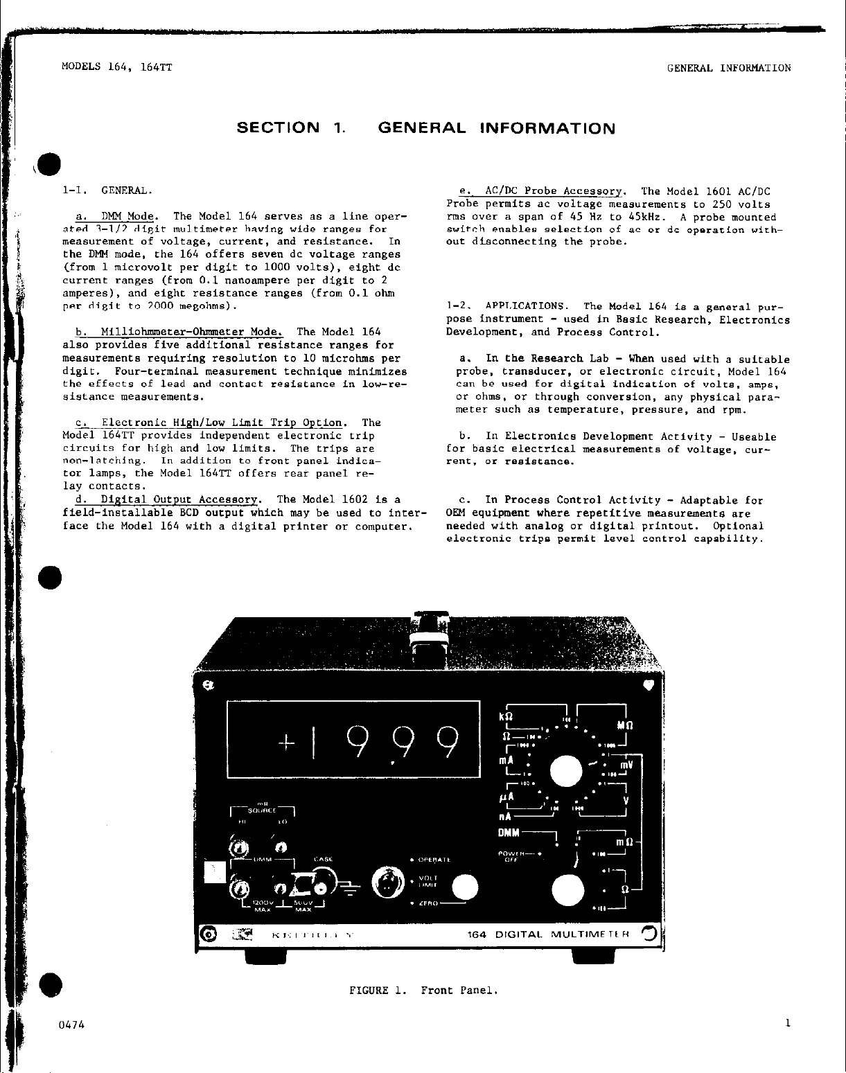
Front Panel
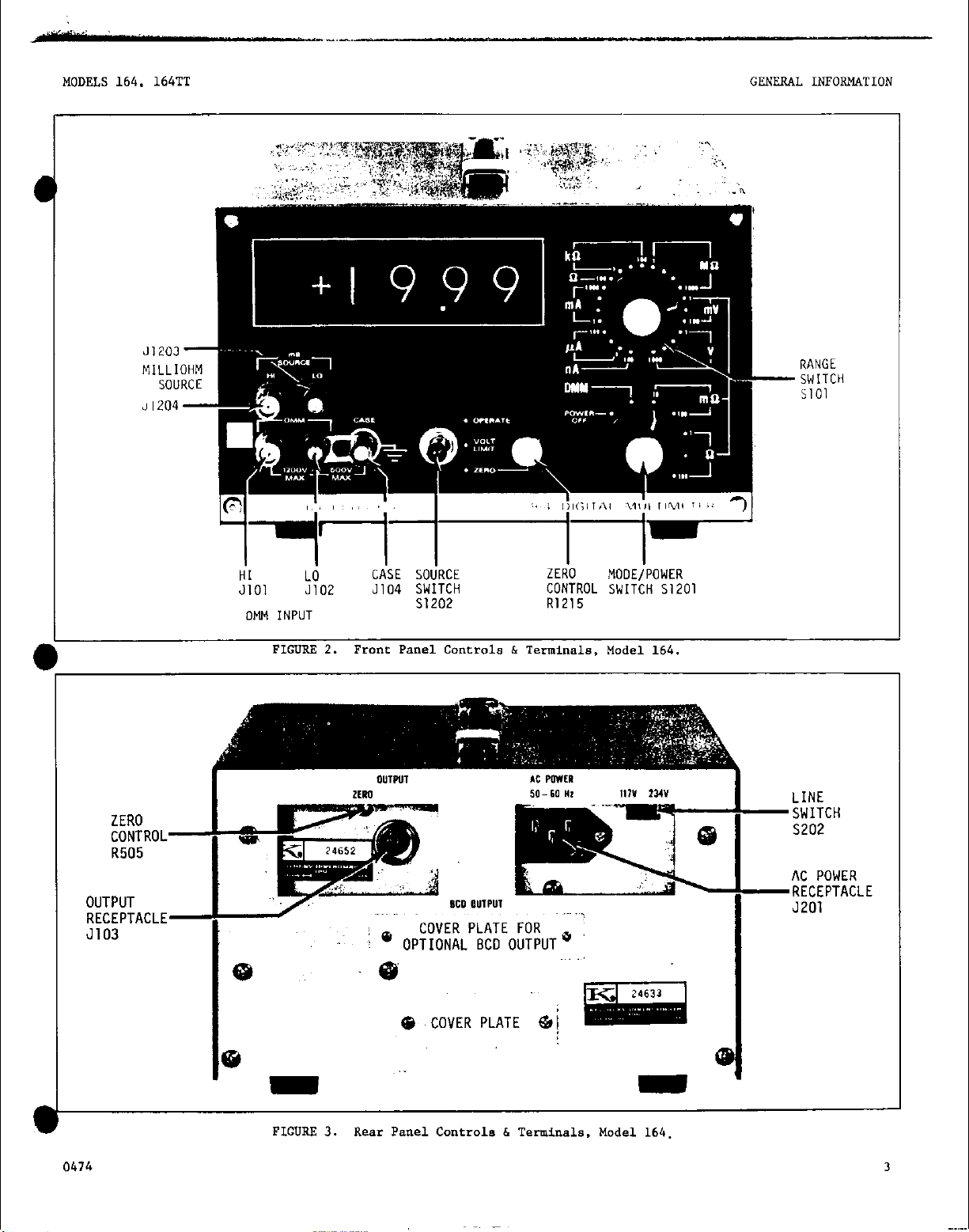
Front Panel Controls b Terminals, Model 164
Rear Panel Controls b Terminals, Model 164
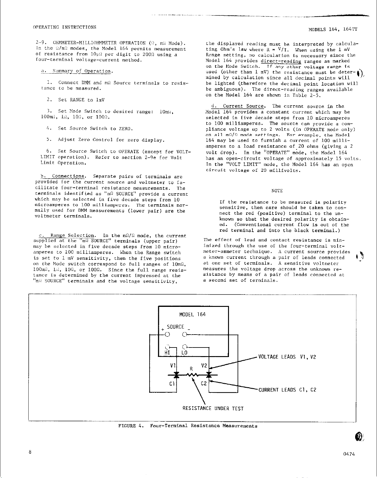
Four-Terminal Resistance Measurements
Timing Diagram for AID COnVerfer
Typical Open-Collector outpue
Pill Designations For Printer output
Front & Rear Panels, Model 164TT
Multimeter Block Diagram
Analog Amplifier Block Diagram
A/D
Converter Block Diagram
Integrator Simplified Diagram
RANGE Knob Assembly
Chassis Assembly
servicing Of Chassis
PC Board I.ocacions
Side View of Chagsis
Chassis, Bottom
View
Calibration Controls
Calibration of Milliohm Current Source
Top Cover Assembly
Botfom cover Assembly
Component Layout, PC-254
Component Layout. PC-251
Component Layout, PC-248
cmlponent Layout, PC-255
Camponene Laywf, PC-250
Component Layout, PC-287
componenr Layout, PC-348
Page NO.
1
3
3
8
12
13
13
14
15
16
18
19
25
25
26
27
28
31
32
34
37
37
50
51
51
52
52
53
54
Page 4
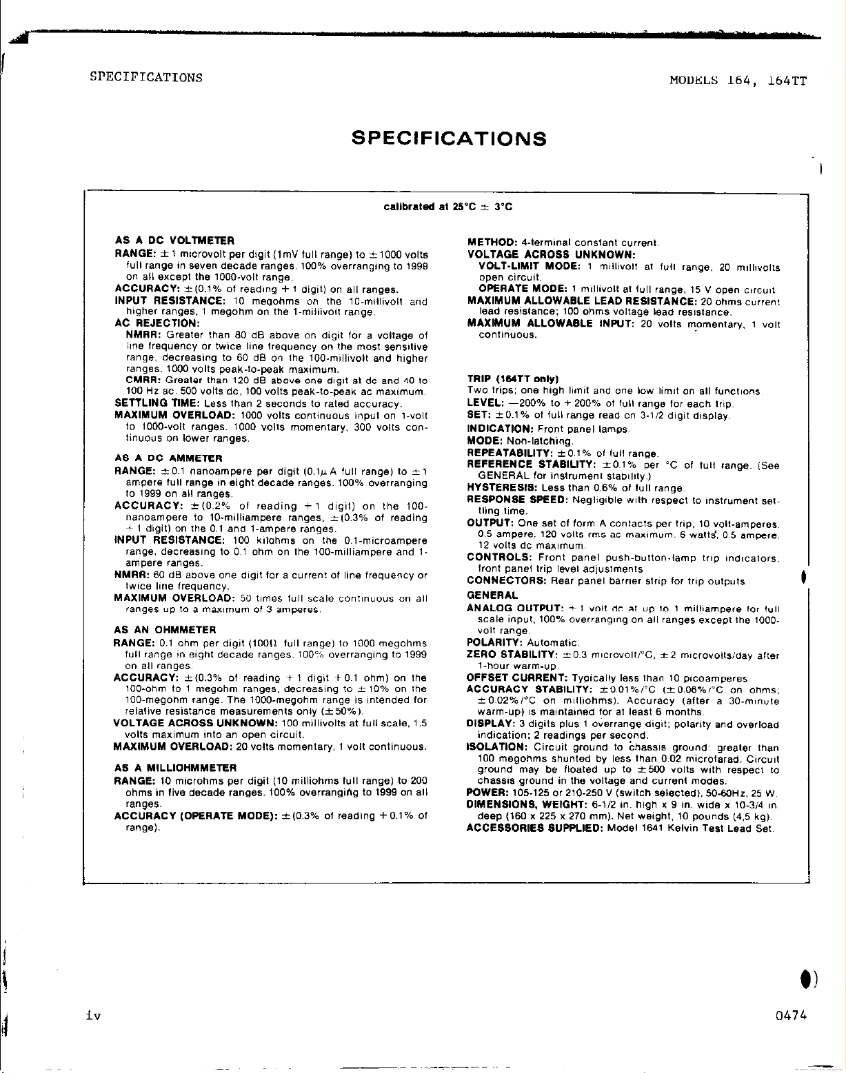
SPECIFICATIONS
MODELS 164, 164TT
SPECIFICATIONS
I
iv
0)
0474
Page 5
Sheet I of I
1275
KEITHLEY
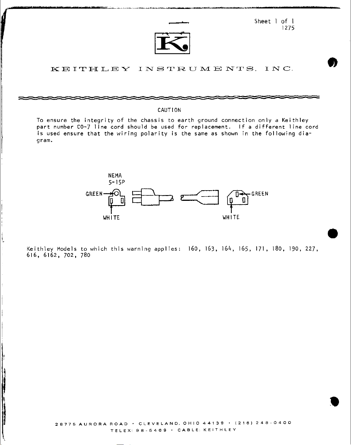
To ensure the integrity of the chassis to earth ground connection only a Keithley
part number CO-7 line cord should be used for replacement.
is used ensure that the wiring polarity is the same as shown in the following dia-
gram.
NEMA
5-l5P
WHiTE WHiTE
INSTRUMENTS. INC
CAUTION
If a different line cord
Keithley Models to which
616, 6162, 702, 780
this warning applies: 160, 163,
164, 165, 171, 180, 190, 227,
Page 6
MODELS 164, 164TT
SECTION 1. GENERAL INFORMATION
l-l.
GENERAL.
a. mm Mode. The Model 164 serves as a line aperated 3-l/2 digit multimeter having wide ranges for
measllrement of voltage, currerlt, and resiseance. I"
the D"M mode. the 164 offers seven dc volrage ranges
(from 1 microvolt per digit to 1000 volts). eight dc
current ranges (from 0.1 nanoampere per digif to 2
amperes), and eight resistance ranges (from 0.1 ohm
per digit LO 2000 megohms).
b. Milliobmmerer-Obmeter Mode. The Model 164
also Provides five additional resistance ra"ze8 for
mas";eme"fa requiring resolution to 10 microbm per
digit. Four-terminal measurement technique minimizes
the effects of lead and contact resistance in 1orresistance measurements.
C. Electronic High/Low Limit Trip option. The
Model 164TT provides independent electronic trip
CirCUitS for high and low limits. me trips are
"on-latching.
to= lamps, the Model 164TT offers rear panel r-elay contacts.
d. Di.sital Oue~ut Accessory. The Model 1602 is a
field-installable BCD output which my be used to interface the Model 164 wit31 a digital printer or computer.
I" addftio" to front pane1 indiG-
GENERAL 1NFORMATION
e. AC/DC Probe Accessory. The Model 1601 AC/DC
Probe permits ac voltage meas”reme”ts to 250
rms over a spa” of 45
Hz Co 45kHr. A probe mounted
volts
switch enables selection of ac or dc operation vichout disconnecting the probe.
1-2.
APPLICATIONS. The Model 164 is a general purpose instrument - used Fn Basic Research, Electronics
Development. and Process Control.
a. I" the Research Lab - When used vith a suitable
probe, transducer, or electronic circuit, Model 164
can be used for
digital indication of volts. amps.
or ohms. or through conversion, any physical parameter such aa temperature, pressure, and rpm.
b. I" Electronics oevelopmene Acriviry - "seable
for basic electrical m?as"reme"ta of voltage. current. or resistance.
@
0474
1
Page 7
GENERAL INFOFwAT1ON
i
Control
MODELS 164. 164~~
TABLE l-1.
l+O"f Panel Controls and Terminals
Paragraph
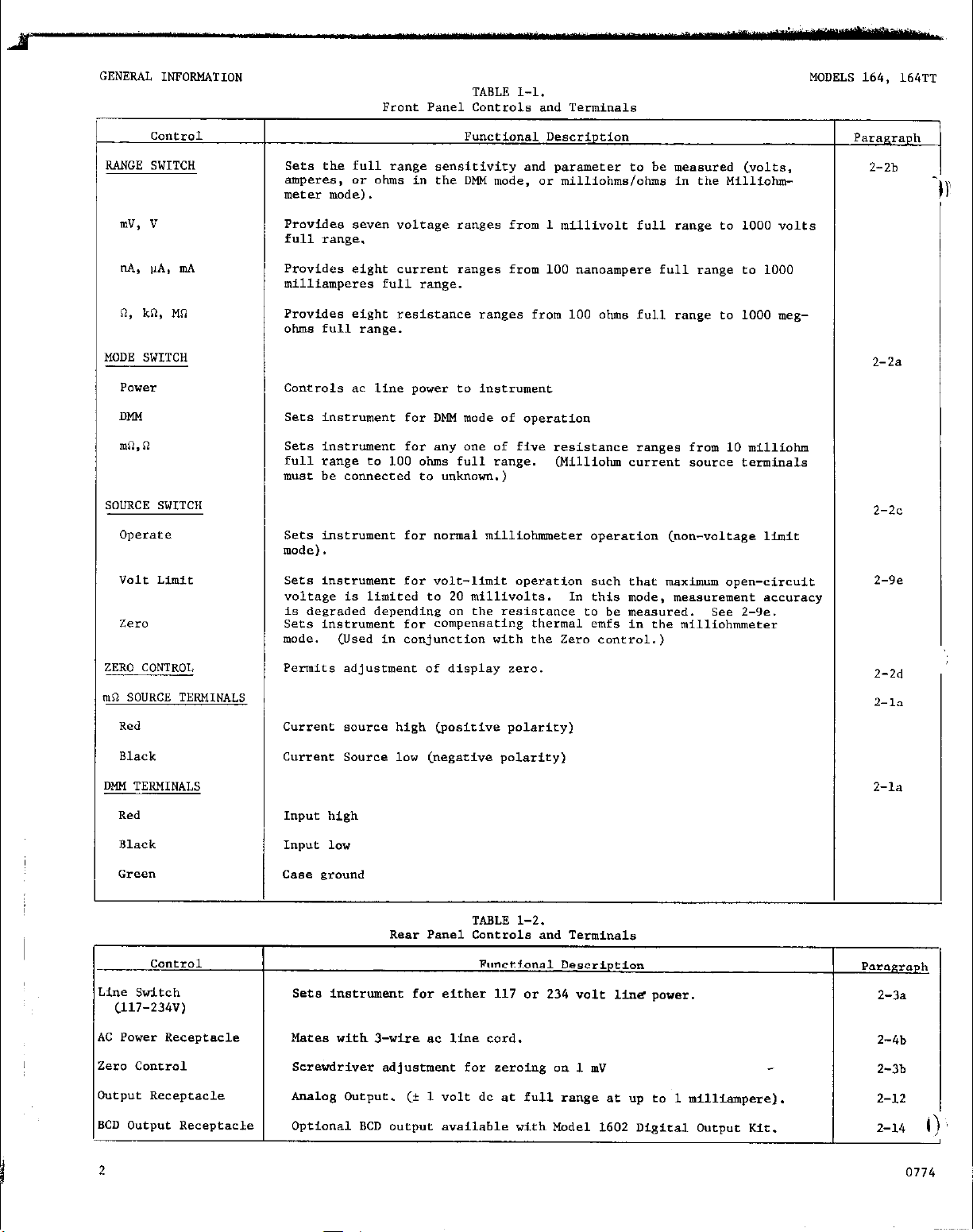
RANGE SWITCH
In", "
"A, IIA. mA
n, krl, MO
Power
DMM
mn,n
SOURCE SWITCH
operate
Volt Limit
Sets the full range seneiei"ity and parameter to be measured (volts,
amperes, or ohms in the D"N made, or milliohms/obms in the Milliobm-
meter made).
Providea S.z"t?" voltage ranges from 1 mflli"olL full range to 1000 "OltS
full range.
Provides eight current ranges from 100 nanoampere full range to 1000
milliamperes full range.
Provides eight resistance ranges from 100 ohms full range to 1000 meg-
ohms full range.
Controls ac line power to insfrument
Sets instrument for DMM mode of operation
sets instrumenf for any one of five resistance ranges from 10 miniohm
full range to 100 ohms full range. (Milliobm current source terminals
m"st be connected to ""know".)
sets instrument for normal millioblmneter operation (non-voltage limit
made).
Sefs instrument for "elf-limit operation such that maximum open-circuit
voltage is limited to 20 millivolts. In this mode, measurement accuracy
is degraded depending on the resistance to be measured. see X-9.2.
Sets instrument for compensating thermal emfs in the milliobmmeter
mode. (Used in conjunction with the Zer" control.)
2-2b
2-b
2-k
2-9e
ZERO CONTROL
nn SO"RCE TERMINALS
I:
Red
Black
I!
Red
Black
I
Line Switch
AC Power Receptacle
1
zero Control
output Recepracle
BCD output Receptacle
Control Functional Description
(117-234V)
Permits adjustment of display zero.
currene source low (negative polarity)
Input high
Input law
Case ground
TABLE l-2.
Rear Panel Controls and Terminals
Sets instrument for either 117 or 234 volt lina power. 2-3a
Mates with 3-"tie ac line cord.
screwdriver adjusrmenr for zeroing o* 1 mv
Analog Output. (r 1 volt dc at full range at up to 1 milliampere).
Optional BCD output available with Model 1602 Digital Output Kit.
2-2d
*-la
Z-la
Paragraph
2-4b
2-3b
2-12
2-14 I
2 0774
Page 8
MODELS 164, 164TT
GENERAL mFOF.MATlON
Jl203
MILL1
SOU
d204
ZERO
CONTROL
R505
OUTPUT
RECEPTACLE
5103
HI
JlOl J102
OMM INPUT
LO
FIGURE 2.
CASE SOURCE
5104 SWITCH
s1202 R1215
FronL Panel Controls h Terminals, Model 164.
ZERO
CONTROL SWITCH 51201
MODE/POWER
RANGE
SWITCH
SlOl
LINE
SWITCH
s202
AC POWER
RECEPTACLE
5201
I
0414
FIGURE 3. Rear Panel Controls b Terminals. Model 164.
3
Page 9
SECTION 2.
OPERATING INSTRUCTIONS
1-l. 1NPUT CONNECTIONS.
a.
“inding Pose Terminals.
L. DMM Mode.
vided o” the front panel for connections EO input
HI (Red), input LO (Black), and chassis ground
(ccee”).
measurements, the source should be conneceed be-
tween the lower set of red and black termi”als.
Tile green rennin=1 may be connected to input LO
by use of a shorting link when grounded operation
is desired. see paragraph 2-11 for a discussion
Of fl”aZi”g operation.
‘. Xilliobmecer Mode. A separate pair of red
and black terminals is provided for use when making
four-rermina1 reSiSLa”ce nleaeurements.
ohm ct~rrent source provides a positive dc current
at ihe iHI (Red) terminal and is used in conjuncrio”
wietl ci,e DMM terminals.
discussion of milliohmeeer operation.
1641 Kelvin Test Lead Set (furnished with the Model
L64) simplifies connections co the resistance to be
measured.
tions for both voltage and current leads without
the need for separate cables.
b. Noise Considerations. The limit of resolution
in voltage and current measurements is derermined
largely hy rhe noise generated in the source. Stray
low-level noise is present in some form in nearly al1
electrical circuits. The instrument does not distinguish between stray and signal voltages since it measures the net voltage. When using the 1 mV and 10 mV
ranges, consider the presence of low-level elecrrical
phenomena such a~ thermocouples (thermoelectric effect,, flexing of coaxial cables (triboelectric effect), apparent residual charges on capacitors (dielectric absorption,, and battery actFan of two dFf-
ferenr contact materials (galvanic action).
1. Thermal Ems. Thermal ‘auf.9 (thermoelectric
porentiale) are generated by thermal differences
between two junctions of dissimilar metals. To
minimize ehe drift caused by thermal emfs, use cop-
per leads to connect ehe circuit to the i”s~rume”t.
The front or rear panel ZERO control cm, be used
to buck out thermal offsets if aecessary.
The KeiChley accessory Model 1483 Low Thermal Connection Kit confains a11 necessary materials for
making very low thermal cop,xr crimp connections
for minimizing thermal effecrs.
For voltmeter, ameter, and ohmmeter
Uinding post terminals are pro-
The rnilli-
See paragraph 2-9 for a
The Model
The Test Lead provides clip-o” connec-
NOTE
The inscrumen~ provides attenuation of line
frequency noise superimposed on an input
signal. The a-c rejection is specified as
f0110!.W:
WXR: Greater rha” 80 dB above one digit
for a voltage of line frequency or rwice
line frequency an the nw5t sensitive range?.
decreasing to 60 dB on the 100-millivolt
and higher ranges. 1000 volts peak-to-peak
mCXXim”m.
CMRR: Greater than 120 dB above one digit
at dc and 40 to 100 Hz ac.
100 volts peak-to-peak ac maximum
Proper shielding as described in paragraph 2-1,~
can minimize noise pick-up when rhe insrrumenc is
in the presence of excessive a-c Eiclds or when very
sensitive measurements are being made.
3. Magnetic Fields. ‘The presence Of strong mag“etic fields can be a potential source of a--c noise.
Magnetic flux lines which cut a conductor can produce large a-c noise especially at power line frequencies. The voltage induced due t” magnetic flux
is proportional to the area enclosed by the circuit
as well as the race of change of maflnetic flux. 2%”
effective wag co minimize magnetic pickup is LO ,’
=rra”ge all wiring SO Chaf fhe loop area enclosed
is as small as possible (such as twisting input leads).
h Second way t” minimize mnR”etic pickup is to use
shielding as described in paragraph 2-1,~.
C. Shielding.
Electric Fields. Shielding is usually “eces-
1.
say, when the instrument is in the presence of very
large a-c fields or when very sensitive measureme”ts
are being made. The shields of the measurement cir-
cuit and leads should be connected together t” ground
at only one point. This provides a “tree” configuration, which minimizes ground loops.
2. Magnetic Fields. Magnetic shielding is useful where very large magnetic fields are present.
Shielding. which is available in the form of plates,
foil or cables, ca” be used to shield the measuring
circuit, the lead wires, or the instrument itself.
500 volts dc,
2. A-C Electric Fields. The presence of electric fields
s”“rceB can have an effect on instrument operation.
A-C voltages which are very large with respect to
the full-scale range sensieivicy could drive the
a-c amplifier into saturafian, thus producing a”
err”“e”“s d-c oq.tpue.
4
generaced
by power lines or other
3. other Considerations.
a) Voltmeter Measurements. “se shielded in-
put leads when so”rcr resistances are greater
than lmegohm or when long input cables are used.
0414
Page 10
MODELS 164, 164TT
b) current Measurements. on the InA CUrrent
ranges, no special shielding precautions need be
taken.
ed input leads are recormended.
put leads and =o”rce are recommended for m===“r=menes an the 10 megohm through 1000 megoh ranges
2-2. FRONT PANEL CONTROLS.
a.
tion of onerafine mode. The DMM oosirio” allows the
Model 164 co be used as a voltme&, ameter, and
ohmmeter. The mn and n positions allow the Model 164
to be used as a four-terminal resistance measuring
instrument.
power to the instrument.
b. Range Switch.
Of function and full range in the mm mode.
“rawever, on the UA and nA ranges, shield-
Power/Mode Switch. This switch permits selec-
The Power OFF pcxition disconnects line
This switch permits selection
3. Zero Posltia”. This position disconnects the
current source from the ““k”0w” for zeroing the
Model 164 in the milliohmeter mode only.
d. Zero Conerol.
,unction with the Source Switch (Zero Position) to
zero the reading in the milliohmeter mode. The co”rral may also br used in the DMM mode for adJustme”ts
on the 1 mV and 10 m” ranges.
adjusrmenr ie also provided for making co==== zero
=d,ustme”fs.) Place a short =cro== “oltm=t=r t=rminals before ad,usfi”g zero in Voltmeter mode.
This conrro1 is uSed in co”-
(A rear panel zero
2. “oltage Funcrio”.
Range Switch are designated in millivolts (mV) and
Volts (“) for full ranges from 1 millivolt to 1000
Volts.
inad”erranL Switching to the nanaampere ranges with
clockwise switch rOCatlo*.
sectors of the Range Switch are designated in ohms
(n), kilohms (K!?), and Megohms for full ranges
from 10” ohms to 1000 megohms.
fors of the Range Switch are designated in “a”“-
amperes (*), microamperes (NY), and milliamperes
(ma), for full ranges from 100 nanoamperes fO 1000
milliamperes.
C. Source Switch.
of operate, Volt Limit, or zero operation when using
rhe mR, n modes.
ma1 operation of the Model 164 as a four-terminal
resistance measuring instrument.
ope”-circ”it voltage of the mi11*otlm current source
to 20 millivolts.
racy is degraded depending 0” the resi=t=“C= to be
measured.
is connected (such as 10 0” the 1Q Range) the I”===urement accuracy is degraded by 5% since a 2On resistance is shunting the input.
A full stop at the 1000 Volt range prevents
Resistance Function. The resisrance (ohms)
3.
4.
Current Function. The current (amperes) s=c-
1. operate Position. This position permits *or-
2. Volt Limit Position.
POT example, if a full range resistance
The voltage sectors of the
This switch permits selection
This position limits the
ln this mode, measurement =CCU-
For maximum operaeor safety, connect the ground wire
of the line cord LO earth ground. This will ensure
that the CASE is at graund potential.
d. Funcfion,Ra”~e Selection. sehxr the PU”Cti0”
and Sensitivity using the RANGE switch.
OHMMETER mode, the RANGE switch is used in co”ju”c-
tion with the MODE Svirch as described in paragraph
2-9.
I” MILLI-
0774
5
Page 11
---.-____I
I
“PERKrING INSTRUCTIONS
2-5. MODES OF OPERATION. The Model 164 permits measurements in either of two modes of operation, 1, Multfmeter ?lode (DMM) or 2) Ohmmeter-Milliobmmeter Mode (n,
mn).
a. Elulrimeter Mode (DMM . 1 I" the DMM mode, rbe
Model lb4 permifs measurement of uolrage, current,
and resiseance (LO 0.U per digit) for conventional
cAeas*relne*ts. To select the DMN mode, set the Mode
Switch to the DMM position.
Switch to the appropriate function and range.
b. Ohmmeter-Milliohmmeter Mode (0, mi2). I" either
thz1 or mil modes, the Model 164 permits mea~"=ement
Of resistance using a four-terminal voltage-current
method. To select the n or mii modes, set the Mode
Smirch to the desired "ohms" position.
rerminals ace provided for cu==ent and voltage se"sing. rhe Model 1641 Kelvin Test Lead Set ifurnish-
ed with the Model 164) simplifies connections to the
resiSta"ce to be measured.
as "m;2 SOURCE" provide a c"==ent in five decades
from 10 microamperes to 100 milliamperes, co==eg-
pending to positions on the Made Switch identi-
fied as IOK?, IOn, I!,, 100m0, o= 10mrt. The ter-
minals normally used for "MB measurements are for
voltage sensing when making four terminal resis-
tance meusurements. The Range Switch Of the Model
164 nl"Sf he set to rile lrn" function when using the
oirmmeter-milliohmmeter modes.
men set rhe Range
Separate
The terminals identified
HODELS 164, 164~
d. Innut resistance.
"f 10 m=whms 0" the 10 millivolt and higher =a"~*,
1 megohm on the l-millivolt range. FO= lomv and
higher =a"Ses, a 1000 ohm source eestatance will
introduce only 0.01% e==o=. 'ro maintain rated acw-i
racy o" the 1mV =a"~. the source reaiseance should
not exceed 100 ohms.
e. Off-Ground Measurements. The instrument low
terminal can be floated *500 volts above CASE ground
for voltage ,~~~%S"re?me"t~. Refer to paragraph 2-11
for complete instructions.
f.
AC Voltage Adapter Probe. The Model 1601 AC/DC
Probe permits convenient a-c voltage meaguremenfs from
0.1 volt to 250 volts rms o"e= a span of 4s HZ to 45
kkh. A probe-mounted switch provides convenient selection of,a-c o= d-c operation without disconnecring
the probe. Therefore, the probe may be pe=manently
attached.
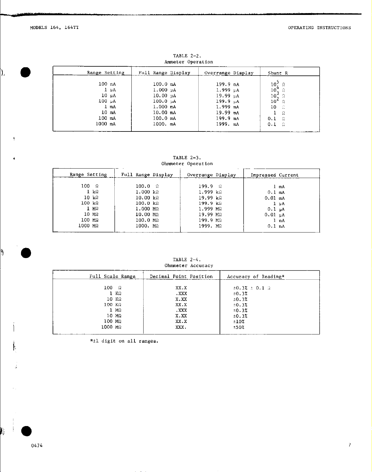
2-7. aMMETER OPERATION (DMM Mode). This mode of
operation enables current meaS"=eme*ts from 0.1 "ano-
ampere per digit (100 nanoamperes full range) to 2
amperes with 100% overranging on all ranges.
a.
Range Selection. To select ammeter operarion,
set the Mode Switch to DMM, the" set the RanSe Switch
to the appropriate full range cu==e"t. As an ammeter,
the Model 164 provides eight ranges as given in Table
2-2.
The input haa a reeist="Ce
VOLTMETER OPERATION @MM Node). This mode of b.
2-6.
operation enables voltage meaS"=eme"eS from il microvolt per digit (1 millivolt full range) to tlOO0 volts.
Range Selection. To select "oltmeLe= operation
se:'the !Iode Switch t" DMM, then set the Range Switch
to the appropriate full range voltage. as a "olr-
meter, the Model 164 provides seven ranges as given
in Table 2-l.
TABLE z-1.
"olmeter operation
Range setcin Full P.a"Se Display Overrange Display
I El
from 300-volt overloads within five seconds on the
lm" range. "p CO 1000 volts peak may be applied
momentarily on any range without damaging the i"st=ument .
1 In”
10
In"
100
II"
1 "
10 v
100 "
"
1000
*Maximum allowable input is 1000 volts continuous inp"t on 1-"OlC to 1000~volt ranges. 1000 volts momentary, 300 volts co"rin"ous on lower ranges.
b. Measurement Accuracy. The voltage a~curac,. is
t(O.l% of reading + 1 digit) on all ranges.
C. Overload Recovery. The instrument will recover
1.000 In”
10.00 rn"
100.0 mv
1.000 "
10.00 v
100.0 v
1000. "
I
1.999
19.99
199.9
1.999
19.99
199.9
1000.
In"
rn"
in"
"
"
"
v*
Co""ecfio*s.
to place the Multimeter in series with the current to
be measured.
C. Measurement Accuracy. The current accuracy is
specified as '0.2% of reading, fl digit on all ranges:
Since the accuracy is specified ac the input terminals,
the loading effects should also be considered. See
Table 2-2 for values of shu"t resisfors.
d.
Off-Ground Measurements. The Model 164 low
terminal can be floated t500 volts above CASE ground
for current measu=eme"ts. Refer to paragraph 2-11
for complete instructions.
2-S. OWMMETER OPERATION @MM Mode). TXhis mode of
operaeion enables resistance meaS"=eme"eS from 0.1
ohm per digit (100 ohms full range) to 2000 megohms.
2,.
Range Selection.
@MM mode), set the Mode Switch to DMM, then set the
Range Switch to the appropriate full range resistance.
As an ohmmeter, the Model 164 provides eighr ranges
as given in Table 2-3.
b. Voltage Across the Unknown. "olfage drop is
100 millivolts at full range with 1.5 V max. into
a" open circuit.
known is determined by dividing the 100 millivolts
by the full range resistance.
c. Maximum Overload.
input tennina1s is 20 voles momentary and 1 Volt
co"ti""o"s.
d. Accuracy. As shown in Table 2-4.
Connect the input twminals so as
TO select ollmmeter operation
Thus the current through the "n-
Maximum voltage ac=oss the
(?
6
0474
Page 12
UA
1
10
II.4
100
“A
ImA 1.000 mA
10 m.4 10.00 mA
100 m.4 100.0 mA
1000 mA 1000. m.4
1.000 LlA
10.00 pA
100.0 DA
TABLE 2-3.
ohmmeter operation
19.99
mA 1 0
199.9 InA
1999.
m.4 0.1 1
0.1 a
Range setting
100 n
1 !4
10 !4
100 kn
1 MST
10 Mn
100 MO
1000 Mn
Full Scale RanRe
Full Range Display
100 n
1 km
100.0 n
1.000 !4
10.00 kn
100.0 kn
1.000 MCI
10.00 MO
100.0 Mn
1000. Mrl
overrange Display
199.9 n
1.999 kl2
19.99 I&
199.9 kli
1.999 MO
19.99 km
199.9 Mn
i
.xXx
x.xX
xX.x
xxx.
1999. Mn
Impressed current
ImA
0.1 mA
0.01 mA
1 “A
0.1 )A
0.01 U.4
1 “A
0.1 n.4
Accuracy of Reading*
to.32 k 0.1 :i
20.3%
10.3%
$0.3%
!O
0474
Page 13
.-
OPEP‘4TING 1NSTR”CTIONS
z-9.
OHMMETER-MILLIOIIMMETCR OPERATION ($2, “!i Mode).
I" the :r,mr moties, the Model 164 permits meaS"reme"t
Of resisrance from lOUS per digit to 2oon "Sing a
four-cermina1 voltage-current method.
d
summary of operation.
1. cannect OMM and ml2 source terminals to resis-
tance LO be measured.
2.
set RANGE ta h"
3.
set ?foLte Switch to desired range:
lOOmA, I::, 102, or 1000.
4. set source Switch to ZERO.
5. Adjust Zero Control for zero display.
6. Set Source Switch tc, OPERATE (except for "OLT-
LIMIT operation). Refer to section 2s9e for "OlC
Limit Operation.
b. cannectians.
provided for rile current source and voltmeter to faCiliCaLe four-terminal resistance measurements.
rermina1s identified as "n& SOURCE" provide a current
which may be selected in five decade steps from 10
microamperes to 100 milliamperes.
mally used for mm meaSureme"tS (lower pair) are the
"oltmeter terminals.
c. Range Selection. I" the mn,n mode, the current
supplied at the "Inn SOURCE" terminals (upper pair)
may be selected in five decade steps from 10 micro-
amperes co 100 milliamperes. when the Range switch
is ser to 1 In" sensitivity, the" the five positions
on ciie Mode svitch correspond to full ranges of 1cmn,
lOOna, 1.2, 1052, or 10057.
tance is determined by the current impressed at the
"l"G SO"RCE" terminals and the voltage sensitivity,
separate pairs of rermina1s are
me terminals nor-
since the full range resis-
l"lDil,
me
MODELS 164, 164'~
the displayed reading tlust be interpreted by calculating Ohm's law where R = V/r. we,, using the 1 m"
RP"c- setting, no calculation is necessary since the
Model 164 provides direct-reading ranges as marked
on the Mode SWiTCh.
used (other than 1 rn") the resistance must be determined by calculation since all decimal points will
be lighted (therefore the decimal p~int location will
be ambiguous). The direct-reading ranges available
on the Model 164 are shovn in gable 2-s.
d. Current Source. The current source in the
Node1 164 provides a constant current which may be
selected in five decade steps from 10 microamperes
to 100 milliamperes.
plia*ce "oltage up to 2 volts (in OPERATE mode only)
on au mnin mode settings. For example, the Model
164 may be used co furnish a currenf of 100 milliamperes to a load resisrance of.20 ohms (giving a 2
volt drop). I" the "OPERATE" mode, the Model 164
has an open-circuit voltage of approximately 15 volts
In the "VOLT LIMIT" mode, the Model 164 has an onen
circuit voltage of 20 millivolts.
If the resistance LO be measured is polarity
sensitive, the” care should be take” to connect the red (positive) terminal to the unknown so chat the desired polarity is obtain-
ed. (Conventional current flow is out Of the
red terminal and into the black terminal.)
If any other "Oltage range is
The source can provide a corn-
NOTE
r),
r
8
FIGURE 4.
MODEL 164
VOLTAGE LEADS Vl,VZ
CURRENT LEADS Cl, C2
RESISTANCE UNDER TEST
Four-Terminal Resistance Measurements
Page 14
MODELS 164, 164TT
OPERATING INSTRUCTIONS
Full Ranges in mn and il Modes
Mode setting hange Setting* (wirh 100% overranping)
0
10 roil
100 mil
1 n
10 !I
100 11
1 m"*
1 Ill"*
1 In"*
1 mv*
1 In"*
*decimal location is valid only when lm" range is selected.
e. Voltage Limit Operation. The VOLT LIMIT mode
limits rhe own-circuit volraae across the m.G SOURCE
terminals to-20 millivolts. This feature is useful
when testing relays and switches to determine if a
"dry circuit" contact is present.
of "dry circuit" measurements, refer to ASTM Specifi-
l
cation 8539-70.)
MeaS”reme”LS performed in VOLT LIMIT InOde
NOTE
(For a discussion
should be used for approx. readi",qs &
since a portion of the mn Source current
is shunted through the limit resisror
(R1210, 1211, 1212, 1213, or 1214) as
shown on schematic 262420.
For “dry circuit:’ testing, set SOURCE switch to VOLT
LILlIT.
If an on-scale reading is indicated. the”
switch to OPERATE mode and record resistance of the
display. If an over-range condition is indicated then
a "dry circuit" open condition is present. since the
valcage is limited to 20 mV, the 164 canmt breakdown
the contact resistance unless switched CO OPERATE
care should be taken t" amid a transient
current pulse which may result from an overshoot of the SOURCE Switch when switching
from ZERO to VOLT LIMIT positions. When
making dry circuit measurements, the recommended procedure is to check the read-
ing in VOLT LIMIT mode, Lhen switch to ZERO
to adjust for zero offsets before taking a
reading in OPERATE.
The transient voltage which can be generated
I
by avershoor of the SOURCE Switch could be as
large as 15 volts. This voltage transient may
be sufficient to explode devices such as det"namrs and squibs if measured in the milli-
I
obmneter mode.
TABLE 2-5.
CAOTION
Max. Reading
mu source
19.99 mn
199.9 mn
1.999
19.99
199.9
!!
.i
'2
100 mA
10 ULA
lti
0.1 mA
0.01 ti
f. Power Dissipation in Unknown. The power dissipated in the unknown is a function of the current
impressed by the Model 164 current source. Power
developed. Worst-case, is dependent on the range selected and the compliance limit.
1. Volt Limit Mode. I” this mode, the compliance
voltage limit is set at 20 millivolts. The w"rst
case power dissipation would be a function of " x I
as shown in Table 2-6.
TABLE 2-6.
10
mn 20 In”
100
mn 20 m”
1
0 20 In"
10
n 20 m"
100
n 20 m"
2.
OPERATE “ode.
I” OPERATE mode, the power
2 InilliwattS
200 microwatts
20 microwatts
2 miCrowattS
0.2 microwatt
dissipation is a funcrion of range selected es
shown in Table 2-7.
g. Milliohmmeter Zero Adjpsc. set the source
Switch to ZERO. the Mode Switch to 10011 (or Lhe desired range), and the Range Switch t" 1 mV. Connecr
the unknown to the four terminals as described in
paragraph 2-9a.
Adjust the Milliohmeter Zero con-
trol to give a zero reading with a flashing r display.
I
.o
0414
9
Page 15
OPmATING niSTR”CTIONS
“erS”S Currenf lneasurements are required. since the
mR currenf source in rhe Model 164 has a compliance
voltage range up to 2 volts, the Model 164 can be
used for material resting or semiconductor diode
checkout using the ranges given in Table 2-8.
V-I Characteristic Measurements
ode setting current Range setting Full Range.
10 mn 100 mA 1 rn" 10 mn
100 mn 10 "IA 1 "I" 100 mn
1 0 lti 1 In" 1 0.
10 n 0.1 n!A 1 El" 10 n
100 ii 0.01 mA 1 In" 100 0
10 mn 100 DA 10 mv* 100 mn*
100 ms2 10 * 10 Ill"* 1 n*
1 n ImA 10 mv* 10 n*
10 0 0.1 mA 10 mv* 100 **
100 n 0.01 In4 10 nlv* 1000 n*
100 nIlI 10 mA 100 "Iv* 10 n*
100 ;! 0.01 mA 100 "Iv* 10 kn*
100 mn 10 mA 1 v* 100 n*
100 P 0.01 m.4 1 v* 100 ki2"
-
10 Inn 100 mA 100 a"* 1 **
1 n 1mA 100 In"* 100 n*
10 n 0.1 mA 100 In"* 1000 n*
10 In<, 100 mA 1 v* 10 **
1 2 1mA 1 v* 1000 cl*
10 !I 0.1 nA 1 v* 10 k&l*
TABLE 2-8.
MODELS 164, 16433
NOTE
The maximum conc~nuous input voltage is
:lOOO volts an the 1000 volf xange.
1. when the Range Switch is placed in Ampere
positions 100 "A through 1000 mA, the MultimeLer
digit.31 display indicates the voltage across a
calibrated, self-contained resistor. The Range
Switch au~amatically selects the calibrated
ran
e resistor for current measurements from 1 x
7
lo-
to 1 ampere full range.
2. The Range Switch is designared in convenient engineering units, "A (nanoamperes), PA
(microamperes) and al.4 (milliamperes) with the
decimal point automatically positioned in the 3
display.
3. me full-scale current is determined by the
Range Switch.
range current ranges available on the Model 164.
Ampere Range
Refer to Table 2-9 for the full-
1 x 10⁻⁷
1.x 10-6
1 x 101;
1 x 1om3
1 x 10⁻²
1 x 10
1 x 10-l
I
t),;
4
,
*NOTE: Decimal point 1ocacion is not indicated when
the Range Swirch is set fo any posirion other than ~mv,
since all decimal points will be lighted. However,
decimal paint can be determined by a sample calculation
uf V : I for a given range.
2-10. DIGITAL DISPLAY OPERATION.
1. When the Range Switch is placed in voltage
positions 1 mv through 1000". the digital display
ind*caCes the actual voltage measured.
2. me Flange SWifCh is designated in convenienr
engineering units, rn" (millivolt*) and " ~"OlCS)
with the decimal point automacica11y positioned in
the display.
3. me full voltage range is determined by the
Range Switch.
4. A" overrange display up to a maximum of 1999
is provided by an overrange "I" Lndicator.
For an input greater than 1999, all digits will be
blanked except the overrange "1" indicator. The
polarity indicator will remain lighted indicating
the correct polarity. TO remo"e an overload condition, change the Range Switch to a lees sensitive
position or decrease the input signal magnitude.
C. ohmmeter Display.
1. When rhe Range Switch is placed in Ohms positions 100 n through 1000 MO, the Multimeter digital
display designates the valrage across the unknown
resistor with a fixed current applied.
2. The Range Switch is designated in convenient
engineering units, 0 (ohms), KO (kilohms) and M,i
(megohm) with the decimal point automatically
positioned in the readout.
3. The full-scale resistance is determined by
the Lange Switch. Refer to Table 2-10 for the full-
range resistance ranges available on the Model 164. ,
TABLE Z-10.
Resistance Display
1 x lo2
1 x 10³
1 x 10⁴
1 x 10⁵
1 x 10⁶
1 x 10'
1 x lo8
1 Y 109
01
/
i
4
0474
Page 16
a. me low terminal can be floated above CASE
ground by removing the shorting link between the I.0
and CASE.
0
ground is greater than 100 megohms shunted by less
than 0.02 microfarad. Circuit ground may be floated
up to k500 volts with respect LO chassis ground in
the voltage and current modes.
b. When the inserument is used far off-ground
voltage or current measurements, rhe low terminal is
at floating potential. The instrument case ground
should be connected to earth ground through the line
and ground terminal.
and CASE must be disconnected.
1salatian from circuit ground to chassis
The shorting link between LO
OPERATING INSTR”CTIONS
h. Set the Range Switch to Amperes positions 1000
mA to 100 "ii while checking the readout so that *era
is indicated 0" all ranges.
i. RemoVe the Short circuit at the input terminals
1. Volts Ranges. me in?.trument will normally
read off zero a small nmount o" the 1 m" through
100 In" ranges because Of sensitivity co random
noise.
ranges 1" through 1000".
a readout overload where all digits except a "1" in
the overrange position are blanked.
indicate a zero readout, except for noise fluctuations.
The readout should remain at zero on the
2.
Ohms Ranges. All Ohms ranges should indicate
3. Amperes Ranges. All current ranges should
4
2-12. ANALOG OUTPUT.
output of 21 volt (non-inverting) at up to 1 milliampere for recording purposes.
ation, the analag 21 volt OUTPUT should not be connected unless a" external recorder is capable of
floating at !500 volts with greater than 100 megohms
iSOl&iO".
2-13. ZERO AD.J”STmNTS.
Short Lhe input terminals with a 10” terminal
a.
connection - preferably a short copper wire or clip
me instrumenr has an analog
For off-ground oper-
range.
C.
set the front pane1 zero control (P.1215) to
the full clockwise position.
If the digital display does not indicate +11
d.
to +13 mv, use the rear panel ZERO Control to adjust
the instrumenr.
e. Readjust front panel zero. zero is indicated
by flashing t polarity lights.
f. Check for zero reading on all ranges fro" 10 In"
to 1000 ".
NOTE
If there is an off zero reading on the 1 volr
range, it "ill be necessary to adjust CT‘? cmRENT OFFSET ADJ. 0" the underside of the chassis.
Refer to Figure 18.
g. set the Range Switch to ohms positions 1000 m
to 100 n while checking the readout so that zero is
indicated 0" all ranges.
j. After the preceding checkout is made, the instrument should be useable for a11 measurements WiCh
no further adjustments necessary.
2-14.
DIGITAl. OUTPUTS AND EXTERNAL CONTROLS.
a. General.
1. The Model 1602 Oigiral Output Kit provides
opriona1 BCO OUtputS and controls.
Included is a 50-pin PRINTEK/CONTROL Connector
2.
(receptacle) for mounting an the instrument rear
panel.
An output buffer card plugs into a prewired
3.
connector on the chassis for either factory or user
installation.
connecting card.
b. OUtpUt Codes and Levels.
The PRINTER/CONTROL 0"fp"tS are Binary Coded
1.
oechl (~0) ~lgnals with I-2-4-8 standard code.
me standard signal levels are as follows:
2.
output l.Qgic "1"
output Logic "0"
3. me Buffer stages uti1i7.e "Open Collector"
O"Lp"t transistors.
Buffer card replaces PC-255 inter-
see Table 2-11 (pg. 12)
see Table 2-11 (pg. 12)
NOTE
If clip leads are used on the input terminals,
the lead resistance may be indicated on the
100 n range since the last digit sensitivity
is 0.1 n per digit.
0474
c. OUtpUt Information.
11
Page 17
OPERATING INSTRUCTlONS
TABLE 2-l'.
Model 1602 Outputs
rJICITAL OUTPUT: Em (1, 2, 4, 8) open collector
logic (Motorola MC 858P) represents each of 3
digits, averrange digit, overload ("I"), polar-
ity (+ = "1"). and decimal position (2 bits).
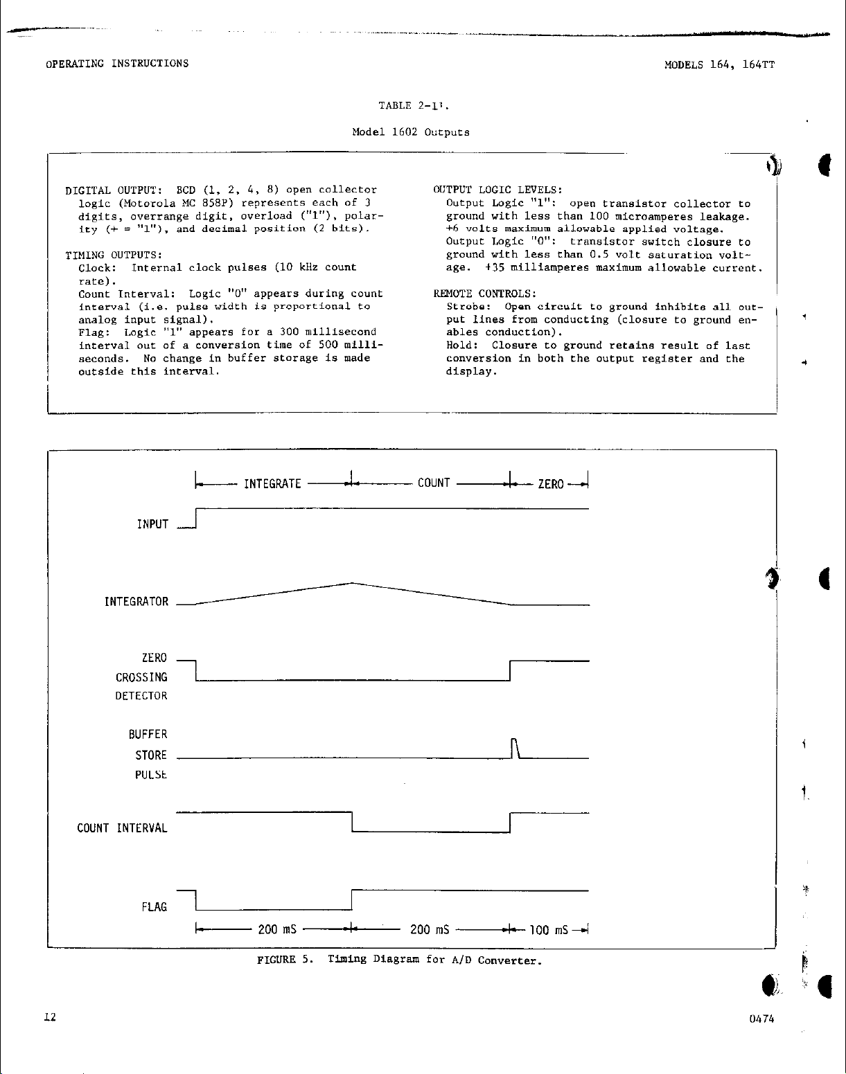
TIMING 0"TPUTS:
Clock:
rate).
count Interval: Logic "0" appears during count
interval (i.e. pulse width is proportional to Strobe: Open circuit to ground inhibits all outanalog inpur signal). put lines from conducting (closure to ground enFlag: Logic "1" appears for a 300 millisecond ables conduction).
interval out of a ~onversio" time of 500 milli- Hold: Closure to ground retains result of last
seconds. No change in buffer storage is made conversion in both the output register and the
outside this interval. display.
~"ternal clock pulses (10 kHz count
OUTPUT LOGIC LEVELS:
output Logic "1": open transistor collector to
ground with less than 100 microamperes leakage.
+6 volts maximum allowable applied voltage.
Ouf~uf Logic "0": transistor switch closure to
ground with less than 0.5 volt saturation voltage. +3s milliamperes maximum allowable current.
REMOTE CONTROLS:
MODELS 164, 164TT
i
i
INPUT
INTEGRATOR
ZERO
CROSSING
DETECTOR
BUFFER
STORE
PULSE
COUNT INTERVAL
I INTEGRATE - COUNT d ZERO-+/
n
FLAG
+ZOOmSA 200mS+lOOmS4
PICURE 5. Timi”! Diagram for A/D Converter.
Page 18
---.
MODELS 164, 164TT OPERATING INSTR"CTIONS
~
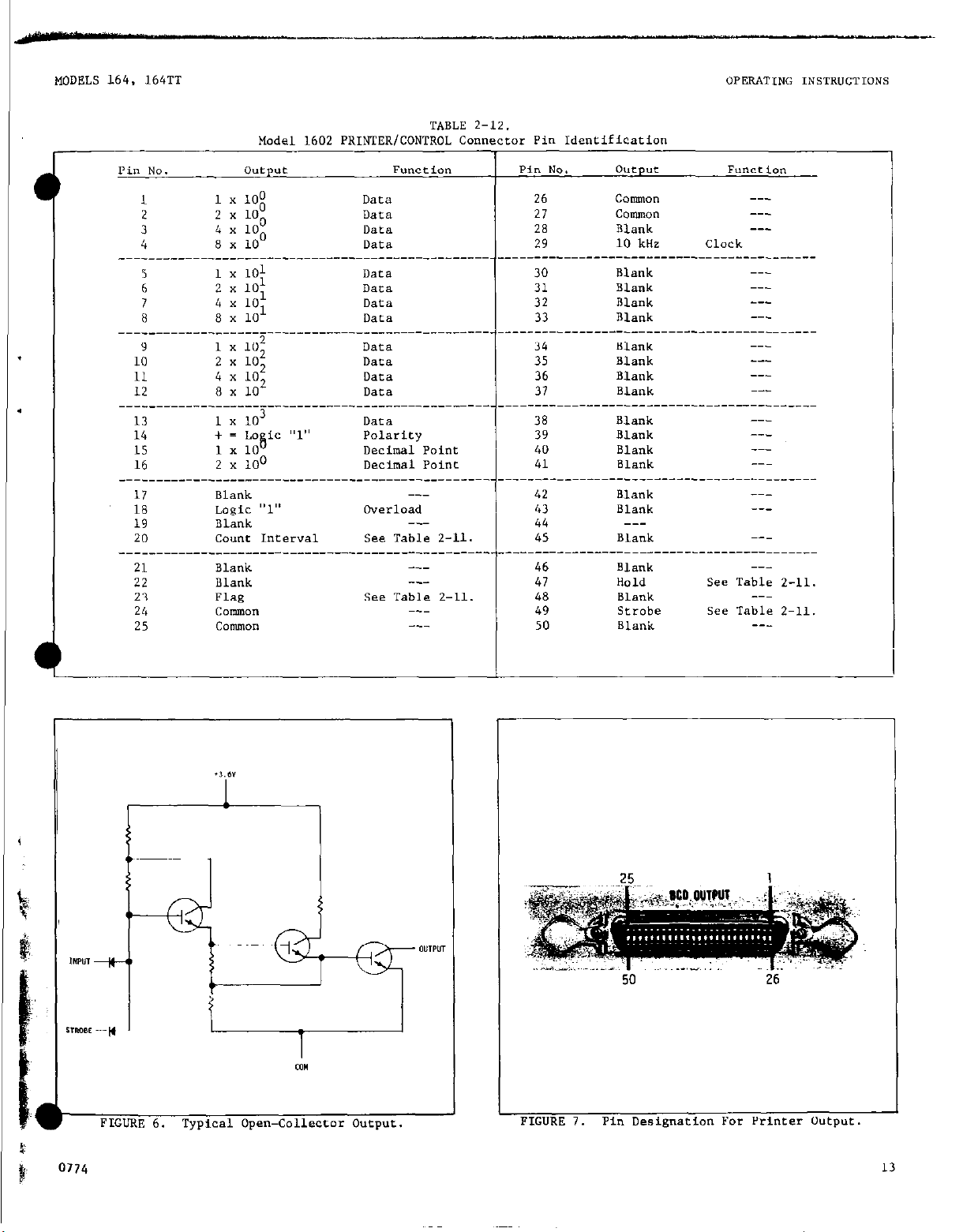
Model 1602 PRINTER/CONTROL Connector Pi" Identification
Pin No.
1 1 x 100
2 2 x
3 4 Y
4 8 x Data 29 10 kHZ Cl‘Xk
_--______---______--------------------------------.------------------------------------~------
* 1 Y 101
6 2 x 101
7 4 x
8 8 x Data 33 Blank ---
9 1 x 10² Data 34 Bh"k
10 2 x lo2 Data 35 Blank _-_
11 4 x lo2 Data 36 Blank ___
12 8 x lo2 Ilate 37 Blank
13 1 x lo3 Data 38 Bh"k
14
15 1 x 10 6 Decimal Point 40 Blank _-_
16 2 x 100 Decimal Point 41 Blank _-17 Blank 42 Blank _--
18 Logic "1" Overload 43 Blank --_
19 Blank 44
20 count Interval see Table 2-11. 45 Blank
21 Blank
22 Blank
23
24 CO*O"
25 COINTIO"
ouepuc Function
loo
100
loo
lo1
101
+ = Lo ic "1" Polarity 39 Blank
Flag
Data 26 COGZIIO"
Data 27 COU!lllO"
Data 28 Blank ---
Data 30 Blank
D.Sfa 31 Blank
rat.3 32 Blank ---
See Table Z-11.
TABLE 2-12.
-__
---
--_
Pi" NO. Output Function
__---____----____-______________________-~~-
46 Blank
47 Hold
48 Blank
49 SLrObe
50 Blank
see Table 2-11.
see Table z-11.
_--
--_
FIGURE 6. Typical Open-Collector Output.
FIGURE 7. Pi” Designation For Printer output.
13
Page 19
OPERATING INSTRUCTIONS
MODELS 164, 164TT
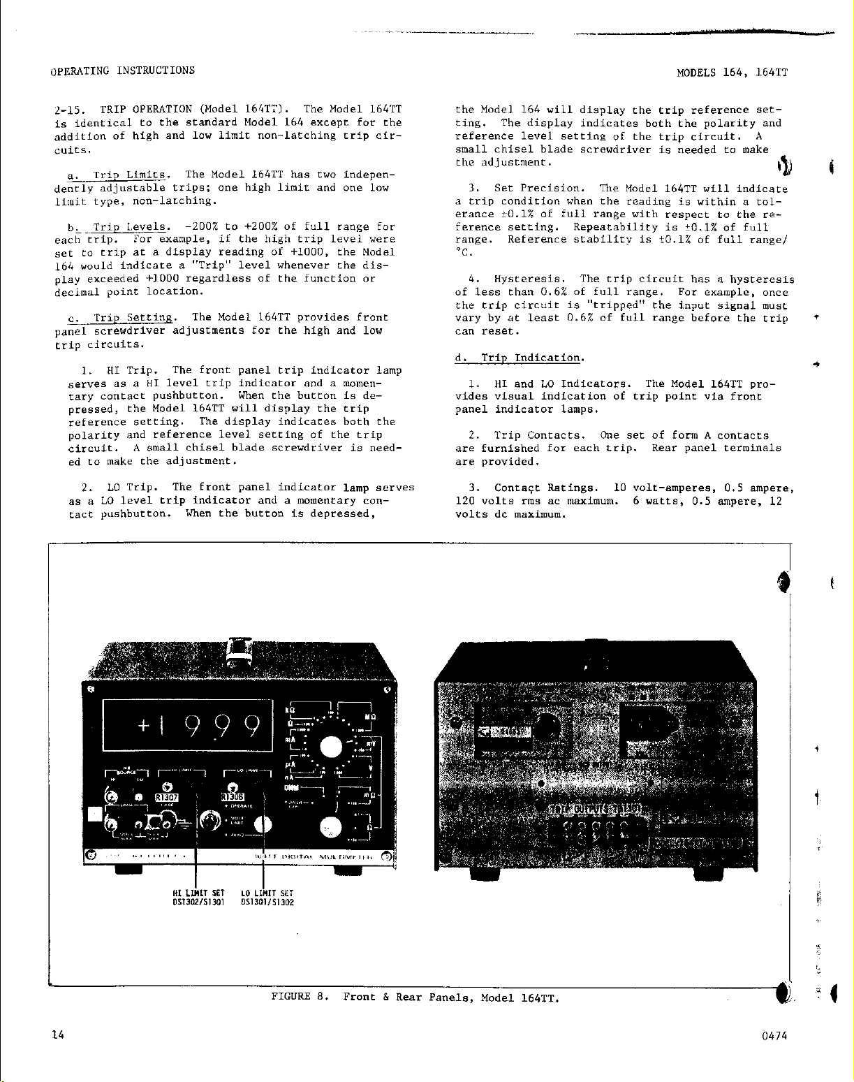
z-15. TRIP OPERATION (Model 164K1. The Model 164TT
is identical to the standard Model 164 except for the
"dditio" of high and law limit "on-latching trip circuits.
a. mip mimics. The Model 164TT has two independenely adjustable trips: one high limit and one low
limit type, non-latching.
b. Trip Levels. -200% to fZOO% of full range for
each trip.
set co trip at a display reading of f1000, the Model
164
would indicate a "Trip" level whenever the display exceeded +I~000 regardless of the function or
decimal puinr location.
C. Trip Setting. The Model 164TT provides front
pa"el screwdriver adjusrments for the high and low
trip circuits.
1. HI Trip. The front panel trip indicator lamp
serves as a "I level trip indicator and a momentar" contact p"shb"tto". when the button is depressed, the Model 164TT will display the trip
reference setting.
polarity and reference level setfing of the trip
circuit. A small chisel blade screwdriver is "eeded to make the adjustment.
2. LO Trip. The front ,mnel indicator lamp serves 3. contap Ratings. 10 volt-amperes, 0.5 ampere,
as a LO level trip indicator and a mmenrary con- 120 volts rms ac maximum. 6 watts, 0.5 ampere, 12
tact pushbutton. When the button is depressed,
For example, if the high trip level were
The display indicates borh the
the Model 164 will display ehe trip reference setting. The display indicates both the polarity and
reference level setting pi the trip circuit. A
small chisel blade screwdriver is needed ea make
the adjustment.
3. Set Precision. The Model 164TT will indicate
a trip condition when the reading is within a mlerance ?O.l% of full range with respect to the reference setting. Repeatability is fO.l% of full
range. Reference stability is iO.1% of full range,
"C.
4. Hysteresis. me trip circuit has a hysteresit
of less than 0.6% of full range. For example, once
the trip circuit is "tripped" the input signal must
vary by at least 0.6% of full range before the trip
can reset.
d. Trip Indication.
1. HI and LO Indicators. The Model 164TT provides visual indication of eriP point via front
panel indicator lamps.
2. Trip Contacts. One set of form A mntacfs
are furnished for each trip. Rear panel terminals
are provided.
"olts dc maximum.
a
Page 20
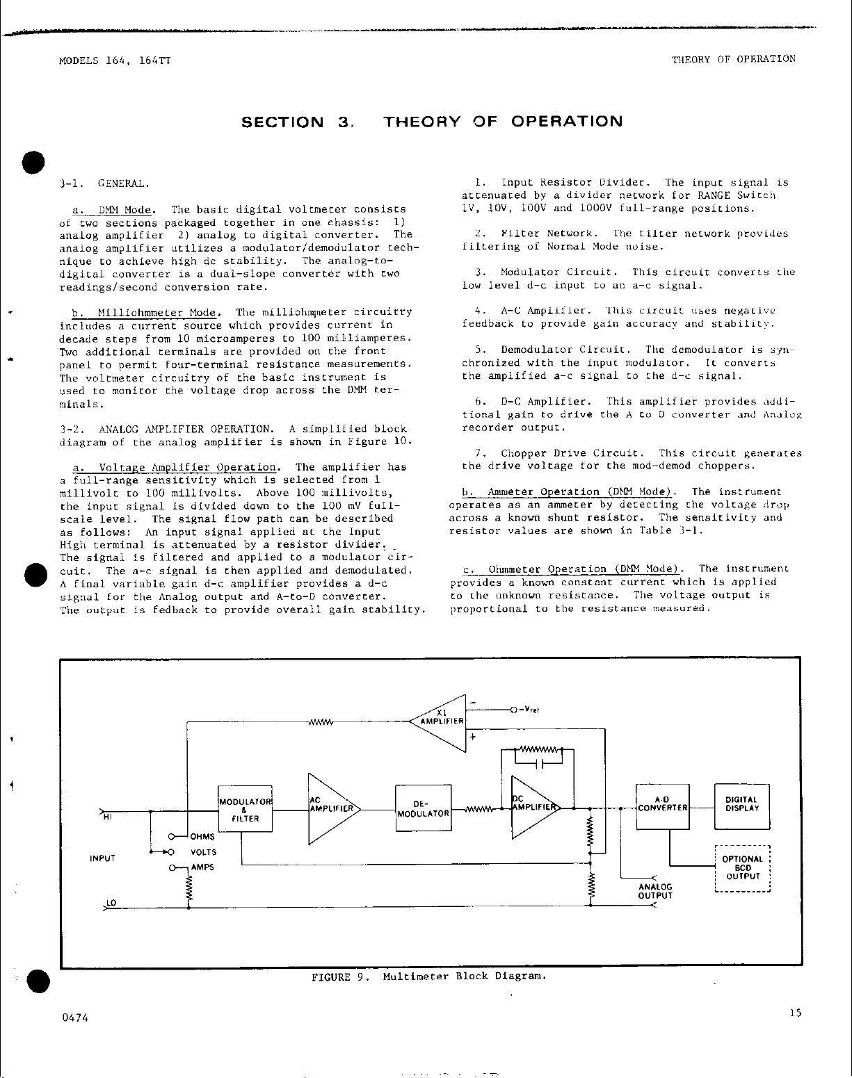
SECTION 3. THEORY OF OPERATION
a. DMM Mode.
ot two sections packaged together in one chassis: 11
analog amplifier 2) analog to digital converter. me
analog amplifier utilizes a modulator/demodulator technique to achieve high dc stability. me analog-todigital converter is a dual-slope converter with two
readings/second conversion rate.
The basic digital voltmeter consises
1.
Input Resistor Divider.
attenuated by a divider network for FU\NGE Switch
IV, 10". 100" and iOOOV full-range positions.
2. Filter Network.
filtering of Normal Mode noise.
3. Modulator Circuit.
law level d-c input to an a-c signal.
The filter network provides
The i"P"L signal is
This circuit converls Lk
b. Milliohmmeter Node.
includes a currene source which provides current in
decade steps from 10 microamperes to 100 milliamperes.
.
Two addiLianal terminals are provided on the front
pane1 to permit four-terminal resistance meaS"renle"tS.
The voltmeter circuitry of the basic instrument is
used to monitor the voltage drop across the "MM Cerminals.
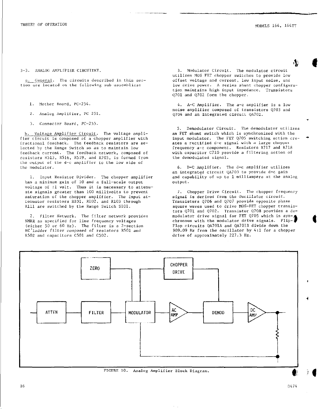
3-L. ANALOC AHPLIFIER OPERATION. A simplified black
diagram of the analog amplifier is shown in Figure lo.
a. voltage Amplifier Operation. The amplifier has
a full-ranee sensitivitv which is selected from 1
millivolt to 100 millivolts. *hove 100 millivolts,
the input signal is divided down to the 100 m" fullscale level.
as fallows: An input signal applied at the Input
High terminal is aetenuaced by a resistor divider,
The signal is filtered and applied to a modulator circuit
h final variable gain d-c amplifier provides a d-c
signal for the Analog out,x,t and A-to-D converter.
'rhe output is fedback to provide overall gain stability.
The a-c signal is then applied and demodulared.
The signal flow path can be described
The milliohqneter circuitry
7. Chopper Drive circuit. 'This circuit generaces
the drive voltage for the mod-demod cho,,pers.
C. OhmmeCer operation (Omltl. me illStr”ne”L
provides a known constant current which is applied
to the unknown resiseance. The voltage output is
proportional eo the resistance measured.
Page 21
--..--
-
MODELS 164, 164~~
- ATTEN - FILTER -
Page 22
Zero Mjustment Circuit. This circuit pro-
8.
vides limited adjustment of zero offset.
composed of potentiometer R505 and resistors 8503,
R504, R506, R508, and R509
and R1215, RI216 (see schematic 26242D).
0’
C. Ammeter Circuit (DKM Made). The instrument
utilizes the chopper amplifier described above with
various Range d&It resistors Rll6 through Pa*.
The chopper amplifier functions as a voltage ampli-
fier to provide an analog recorder output and drive
for the *-to-D converter.
TABLE 3-1.
d. clhmmerer circuit (DMM Mode). The i”strume”t
provides a constant--current using a voltage reference amplifier and series resistor R. The reference
voLtage E limits the open-circuit voltage to 1.5
volts maximum. The voltage reference is composed of
integrated circuit QA704 and reference diode 0702.
l e.
9
f$
to
Milliohm source.
1. AC voltage from T1201 is rectified by bridge
01201, filtered and supplied to the pre-regulator
QA1201. This is a three-terminal 15 volt regula-
tor. me 15 volt O”tp”f is connected through the
series pass transistor 41201 to the Hi terminal of
the rnll source, 31204.
The pass transistor is controlled by the op-
2.
ertional amplifier Q.41202. One input to QA1202 is
+10 voles (referred to power supply con!mon). This
is obtained from LWO zener diodes, 01202 and 01203
and a divider network R1202, R1203, and RlZO4.
R1203 is a potentiomeLer to permit compensation for
the tolerance of the zener diodes and the offset
voltage of QAlZOZ.
drop across the selected current sensing resistor,
one Of R1205 ehrou’gh R1209, which is in series with
the LO terminal, 51203.
3. When the current regulator is in balance, the
drop acroSS the current sensing resistor is qua1
eo the reference valtage and the current delivered
by the rnli source terminals is the proper value.
4. 1f the current source has no load, the volt-
age aCrOSS the terminals will approach 15 vo1rs.
when testing switches or relay contacts for “dry
circuit” applications, the voltage must be limited
to mm” or less. This is done by setting s1202 in
the Volt Limit position. The O”tp”c current is
then divided between the had and one of the volt
limit resistors, R1210 through R1214. Even with
open-circuited load, the volrage at the source terminals will not exceed 2Om”.
(See schematic 262420)
The other input is the voltage
(See schematic 26244E)
It is
3-4.
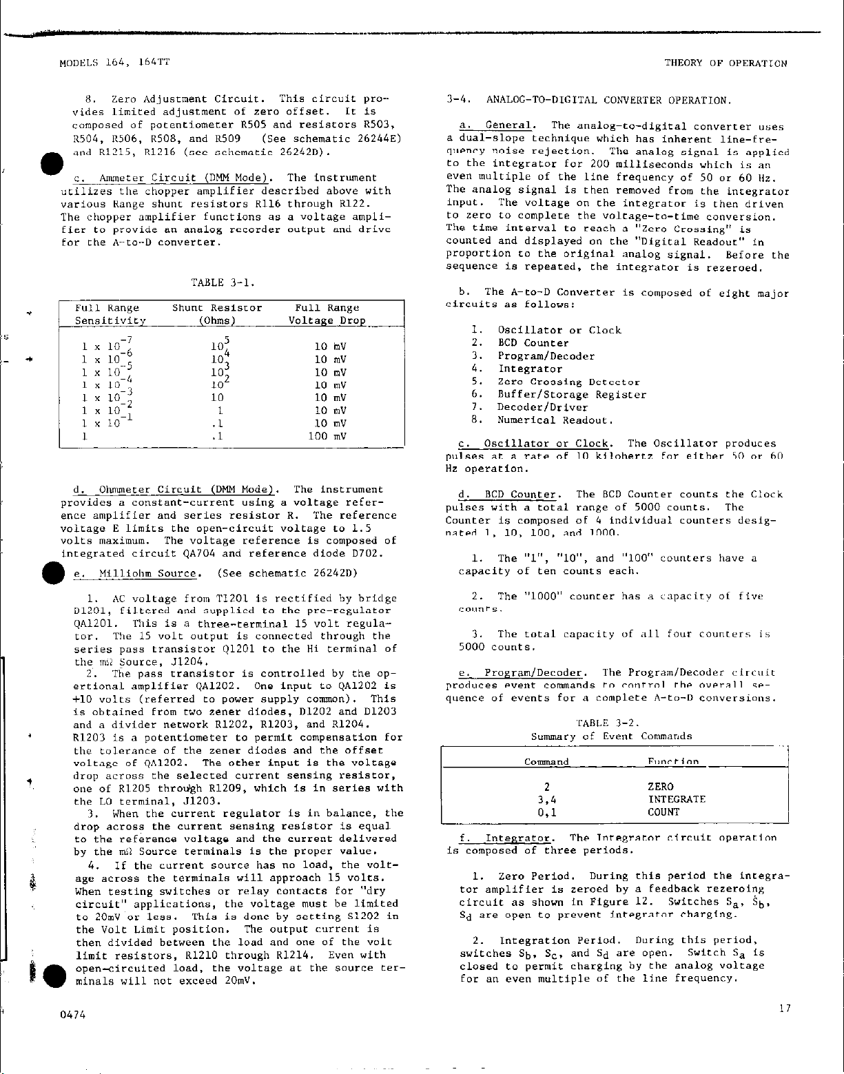
ANALOG-TO-DIGITAL CONVERTER OPERATION
a.
Ge”eC.d.
a dual-slope technique which has inherent line-frequency noise rejection. The analog signal is applied
to the integrator for 200 milliseconds which ia an
even multiple of the line frequency of 50 or 60 HZ.
The analog signal is then removed fram the integrator
input. The voltage on the integrator is then driven
to zero to complete the “olcage-to-time CO”“ersio”.
The time interval LD reach a “zero crossing” is
counted and displayed on the “Digital Readout” in
proportion to the original analog signal.
sequence is repeated, the integrator is rezeroed.
b.
The A-to-D Converter is composed of eight major
circuits as follows:
1. Oscillator or Clock
2.
BCD counter
3.
Program/Decoder
4. Integrator
5. zero crossing DeLector
6.
Buffer/Storage Register
7. Decoder/Dri”er
8.
Numerical Readout.
C. Oscillator or Clock. The Oscillator produces
pulses at a rate of 10 kilohertz far either 50 or 60
HZ operation.
BCD Counter. The BCD bunter COU”LS the Clock
d.
pulses with a total range of 5000 counts.
counter is composed of 4 individual counters designated 1, 10, 100, and 1000.
1. The “l”, “lO”, and “100” counters have a
capacity of ten CoUntS each.
2. ‘rhe “1000” counter has a capaciry of five
CO”ntS.
e. Pro.qram/Decoder. The Pro~ram,Decoder circuir
produces event cownands co conrrol the overall sequence of e”e”eS for a complete A-to-D conversions.
I
f. Infesxrator. The Integrator circuit operation
is composed of rhree periods.
1.
Zero Period.
tar amplifier is zeroed by a feedback rez.eroi?i:
circuit as shown in Fi&~re 12.
Sd are open to prevent integrator charging.
2.
Integration Period.
switches Sb, S,, and Sd are open.
closed to permit charging by the analog voltage
for an even multiple of the line frequency.
The analog-co-dfgical converter uses
2
3.4
0.1
‘TABLE 3-2.
Function
ZERO
INTEGRATE
COUNT
During this period the integra-
Switches Sa, Sb,
During this period,
Switch S, is
summary of Event Commands
Colmn.s”d
Before the
The
i
0474
17
Page 23
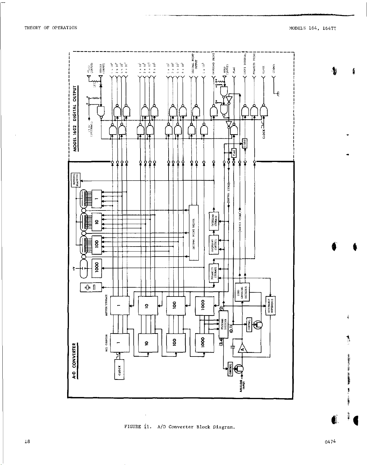
FIGURE 11. AID converter Block Diagram.
I
18
0474
Page 24
I- ~.
,- ----- .-.. -
-I_.
3. Discharge Period. During this period, witch
S, is open to prevent further charging by the analog signal.
drive the Integrator voltage t” zero. A reference
current of opposite polarity t” the input current
is applied through either switch SC or Sd. ‘The
Discharge Period ends when the Zero Crossing Deiec-
tar circuit detects a zero Integrator output.
8. Zero Crossing Detector. The Zero Crossing Detector circuit oravides a “Hieh” or “Low” level output depending on the polarity of the detected input.
Refer to Table 3-3 for a description of voltage ““tputs of the Zero Crossing Detector.
Buffer/Storageister. The Buffer/Storage
h.
Register is composed of “flip-flops” arranged t”
copy the states of the various BCD cou”fers. The
Buffer/Storage Register requires a Buffer St”re corn-
man* before any information ca” be transferred.
The “flip-flop” circuits provide coded information
for Decoder/Drdver and BCD outputs.
Decoder/Driver.
i.
decodes the BCD informatia” from the Storage Register into ten-line decimal code. The Driver circuit
then drives the proper numeral in each of the Num-
Either switch S, or Sd is closed to
The Decoder/Driver circuit
erical Readout tubes.
l j. Numerical Readout.
sists of four numerical indicarors and one oolaritv
indicator drive” by the Decoder/Driver, Pol&ity and
Overload Drivers.
The Numerical Readout con-
k. Summary of Operation. The operation of the
A-Co-D Converter can be described bv considerinr
a zypical conversion cycle. The Cl&k provides..
pulses at a rate of 10 kilohertz.
serves as a master timing control for rhe A-to-D
conversion cycle.
the “1000” counter which has five coded states,
namely 0, 1, 2, 3, and 4.
controls the sequency of commands based on the
coded states from the BCD Co”“Ler.
commands are described as shown in ‘Table 3-2.
“2” command initiates the integrator ZERO period
which removes any residual charge on the incegratar capacitor.
INTEGRATE period which permits a” integration of
the analog signal. At the end of the INTFGRATE
period, the “0.1” command initiates the COUNT period
When the “3,4” command is give”, the integrator is
charged by the analog signal for a period of 200
milliseconds.
the analog signal is removed and the integrator
‘JUtpUt is driven co zer” by a reference current.
The Zero Crossing Detector senses a zero crossing
of the Integrator output and removes the reference current.
show” in Table ,-3.
vided for control of ihe 1nregraror and Palarity
Storage Register. A pulse command is also produced to iniriate a Buffer/Stare.
Score command is give”, the Uufferlstorage Regiarer
copies the *CD Counter states at that lnstan~ of
time.
is the” avail.6l.e for the Decoder/Driver and external printout. The Decoder/Driver decodes the
Buffer/Storage output and drives the Numerical
Readour for a digital display. The conversion.
cycle is completed when the BCD Counter reaches
2000 counts and the PragramlDecoder provides a
“2” command to initiate a new conversion cycle.
The BCD coded infarmario” in the Register
The Liming is accamplished by
‘The Program/Decoder
The “3.4” command initiates rhe
When the “0,l” command is give”.
The Detector provides outputs as
The Cl.5 “OlC levels are pro-
‘The BCD Counter
‘The decoded
The
When the “uifer,
Page 25

‘THEORY OF OPERATION
MODELS 164, 164TT
b.
Oscillator circuit. The osci11aror circuit is
located on a Dorfio” of Drinted circuit assembl” PC-
254. Transis;ors 4601 aid 9602, capacitors C6Oi,
C602. and C603 and resistors R606 and ,607 form an
"SCillatOr. Potentiometer R605 is used to provide
internal screwdriver adjustment of the oscillator
frequency. Transistor 9603 serves as an emmitterfollower co reduce OUtpUt impedance. The chopper
drive is obtained by dividing dowrl the oscillator
frequency from 10 Kilohertz to 909.09 Hz using integrated circuit QA801, a 11:l Divider circuir.
c. Tube Ilaard. The Tube board conrains portions
of five major circuits: the BCD counter, the Program/Decoder, the Buffer/Storage Register, the Decoder Driver, and the Numerical Readout.
1. BCD counter.
a) The Decade counters designated "1". "lo",
and "100" are composed of individual integrated
circuit modules QA308, Qh309, and q.4310 respectively.
b) The "1000" counter is composed of integra-
ted circuit modules QA301A, QA302A, and QA302B.
1. Integrator Circuit. The operation of the
Integrator is controlled by the positions of
switches S.3, Sb, SC, and Sd (as shown in Figure 12).
Switch Sa is Q401.
Transistors 9404, 9405, 9408, Q409, and 9410 are
control circuits arranged to canrra1 the proper FET
switches depending on the signals at pins 12 and
The integrator amplifier consists of tran-
13.
sisters Q402 and 9403 and integrated circuit QA401.
The feedback capaciror is C406.
control the current far 9-volt zener diodes 0401
and 0402. Resistors R403, R404, R405, R409, ~410,
and R.411 are full-scale calibration resistors.
Potentiometers R402 and R408 are internal screwdriver calibration adjustments.
Zero Crossing Detector Circ"it. The high
2.
gain amplifier is composed of cascaded amplifiers
QA402 and QA403.
bias supply for 9.4403 and the output resisror network R444 and R445. The level-splitter circuit
consists of diodes D414 and D415, resistors R443
and R446 and gates QA404 (A and 8).
Switch Sb is transistor Q411.
Switches s, and Sd
Diode 0411 provides a 6-volt
b
+
+
2. Program/Decoder.
of gates Qh304A. QA304C, 9,005 CL?, C, D, E, '3)
QA306.4 and Q.43078.
cOrnposed of integreted Circuit modules QA311,
QA312, and QA313.
4. Decoder Driver. This circuit is composed
of integrated circuits Q.4314, QA315, and QA316.
5. Numerical Readout. "301, "302, "303 are
Readout Tubes ior Units, Tens, and Hundreds respectively.
6. Other circuits contained on the Tube Board
are described as follows:
a) overrange rndicaror Circuit. This circuit is composed of integrated circuit module
QA3018, traneiefor Q301 and overload indicator
DS301.
b) Polarity Indicator Circuit. This circuir
is com,msed of transistors 9305 and 9306 and
Polarity indicator module DS302.
c) Display Rate/Hold circuit. oaees q*303
(A, B, C, D) and QA304B, QA306B, and QA307A
provide capability for Display Rate and "Old
functions when use.3 with additional output
Buffer circuits.
This circuit is composed
3-6. POWER SUPPLIES.
a. t15 Volt supply.
1. The 15 volt supplies tap a--c power from a
secondary winding of transformer T201. Diodes
0203 (A, B. C, and D) and capacitors C204, C205,
C209, and C210 compose a full-wave rectifier with
filtering.
2. The +15 "DlC regulator CirC"it utilizes
3. Transistors 4211 and Q212 form a differential
amplifier which compares the voltage at R218 with
respect to low. The difference voltage is amplified by transistor Q210 and fed to Darlington transister pair, Q207 and 9208, which series regulate
the -15 volt OUtpUt.
Current output to approximarely 200 milliamps.
Transistor q209 limits the
4
+
i
g
20
0474
Page 26

MODELS 164, 164TT
THEORY OF OPERATION
b. +3.6 Volt Supply.
1. The +3.6 volt supply taps a-c power from a
secondary of transformer T201. Modes D2Ol and
0202 and capacitor c201 form a full-wave rectifier
0
with filtering.
Transistor Q205 amplifies the difference be-
2.
tween rhe +3.6 output and a reference voltage derived from the +15 volt supply and determined by
resistors R203 and R204.
The difference voltage
is applied by transistor 4204 which drives a Darling-
ton transistor pair, Q201 and Q202. The Darlint?
ton pair series regulates the +3.6 volt output.
C. +210 Volt 0ufp"f. l The +210 "OIL supply is an
unregulated voltage supply using the half-wave fil-
tered voltage at diode D206 and capacitor c212.
d. +170 Volt output.
1. Regulator. The +170 volts is derived from
the +210 "01~s at emitter of Q302 which series regulates the +170". Transistor Q303 provides a reference for the base of transistor Q302.
2. Lnanking circuit. This circuit controls the
Cl70 voltage for the three right hand readout tubes
The "Q" output of Q.43078 drives the base of tran-
sisror 4304 for nomal re@aror o~eratian. When
an overload occurs, the "Q" output is law turning
off transistor Q304. This results in a drop of
the +170 volt output causing blanking of the read-
0
out tubes.
e. MllliOhrn source supply. The primary windings
Of T1201 are conneceed in parallel with transformer
T201. AC power for both is supplied from line connector P201 via fuse F201 and switch s1201. The dual
primary windings are connected in parallel by switch
S202 for 117 volt operation and in series for 234
Volt operation.
I" addition, fuse F202 is connected
in the circuit for 234 volts.
3-7. ELECTRONIC TRIP CIRCUITRY. The IWO trip circuits in the 164TT are essentially the same, differing only in that the LO trip output eransistor is a"
NPN type while the HI trip output transistor is a
PNP. The analog signal at 5103 (schematic 26244EI
is a one volt signal for full scale input to the mm.
This signal is applied to the *nverting inputs of
QA1301 and QA1302 through resistors RI309 and ~1314.
The reierence voltage used to determine the trip
point is derived from rener diode D1301. The HI
limit is set by RI307 and the Lo limit by R1308.
These limit voltages, either of which may be set
from -2 volts to c2 volts, are applied to the non-
inverting in,mrs of Q.41301 and QAI302 through resis-
tars RI310 and R1315.
If the HI limit is set at
+1.0 volt and the analog output is less than +1.0
volt, Lhe output of QA1302 will be positive and the
HI output transistor 91302, will be cut off. "he" tile
analog o"t~"t exceeds +l.O volt, the o"t~ut of QA1302
Will become negative, turning an Q1302 and causing
relay K1302 to close and lighting the front-panel
trip lamp 051302. A small voltage is developed across
R1320 which is connected back co the non-inverting inPUC of QA1302 through resistor R1317. This provides
SOme hysteresis so the relay will not drop 0°C until
the input is somewhat less than the trip point. The
LO limit CiPz"iC functions the same way except the
out,,ut of Q.41301 is normally negative. since the
*river transistor QlSOl is an NW, it is C"Z off by
this2 voltage. setting the trip points is done by
holding in s1,01 or 51302 and adjusting the correspending limit control, RI307 or Rl308. When the HI
litniL switch 51301 is operated. the analog OUtpUt of
the mm is disconnected from the A/D converter. The
output of QA1302 is connected to the A/D con"erter
and also to the inverting input of QA1302. making it
into a unity-ga*n voltage follower for the trip paint
voltaRe a,qlied to the "an-inverting input. Thus the
A/D converter indicates the magnitude Of the trip
paint voltage.
21
Page 27
MODELS 164, 164TT
SECTION 4.
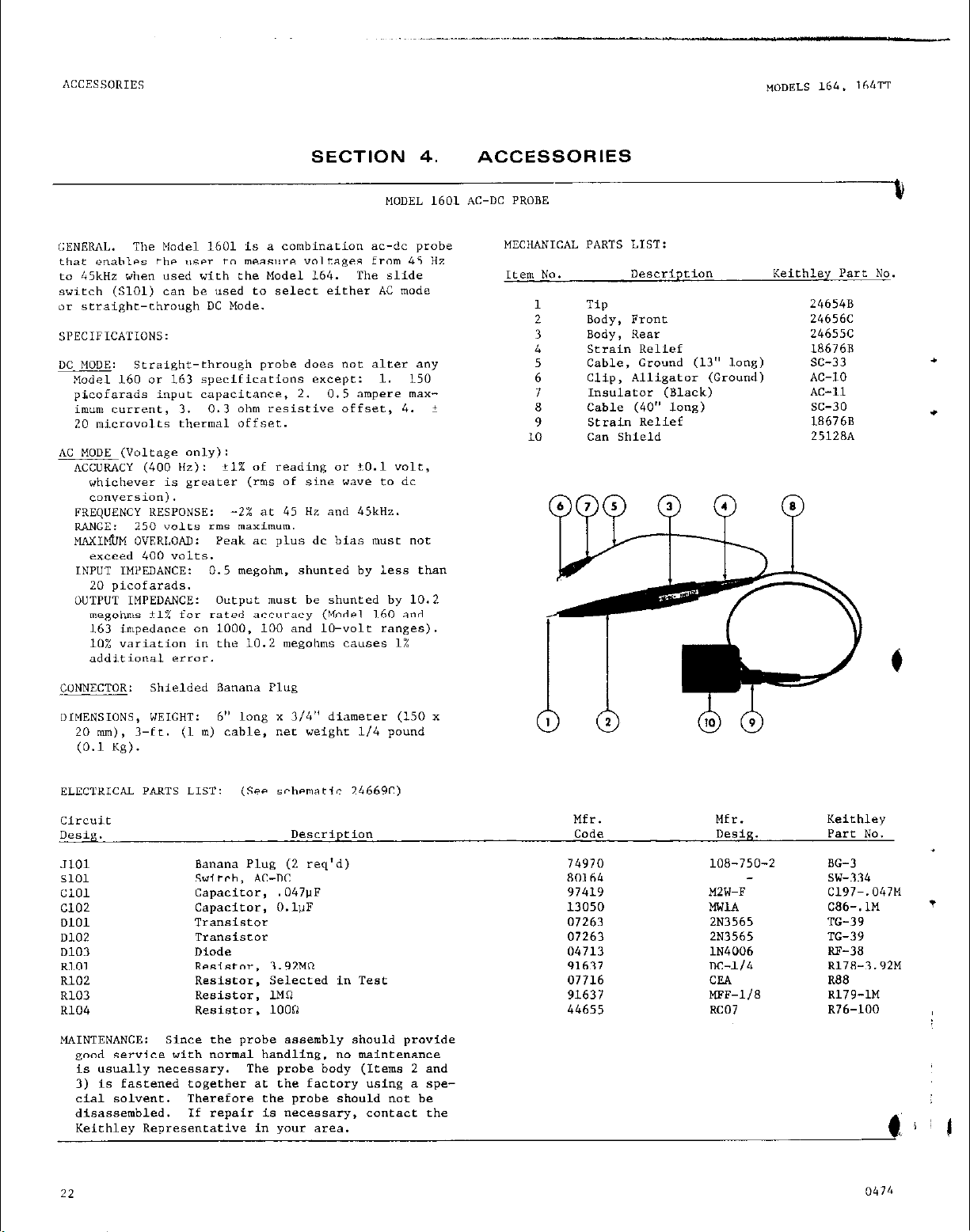
MODEL 1601 AC-DC PROBE
GENERAL.
rtlar enables the user to measure voltages from 45 HZ
to 45kHz when used with the Model 164. The slide
switch (SlOl) can be used to select either AC mode
or straight-through DC Mode.
SPECIFICATIONS:
-:
Model 160 or 163 specifications except: 1.
picofarads input capacitance, 2. 0.5 ampere max-
imum current, 3. 0.3 ohm resistive offset, 4. A
20 micravolrs thermal offset.
AC MODE (Voltage only):
ACCURACY (400 Hz): tl% of reading or to.1 volt,
FREQUENCY RESPONSE: -2% at 45 Hz and 45kHz.
KANGE: 250 volts rms maximum.
MAXIMTIM OVERLOAD: Peak ac plus dc bias miist not
INPU'T IMPEDANCE: 0.5 megohm, shunted by less than
OUTPUT IMPEDANCE: O"t~"t must be shunted by 10.2
CONNECTOR: Shielded Banana Plug
The Model 1601 is a combination ac-dc probe
Straighf-through probe does not alter any
150
whichever is greater (rms of sine wave to dc
conversion).
exceed 400 volts.
20 picofarads.
megohnis il% for rated accuracy (L%udel 160 and
163 impedance on 1000. 100 and IO-volt ranges).
10% variation in the 10.2 megohms causes 1%
additional error.
ACCESSORIES
Itern NO. DCXriptiO" Keithley Part No.
1
2
3 Body, Itear 2465X
4 strain Relief
5
6 Clip, Alligator (Ground)
7 Insulator (Black) AC-11
8
9 strain Relief
10 Can Shield 25128A
TIP
Body, Front
Cable, Ground (13" long) SC-33
Cable (40" long) SC-30
246548
24656C
18676B
AC-10
186768
li
*
*
4
DIMENSIONS, WEIGHT: 6" long x 314" diameter (150 x
20 mm), 3-ft. (I m) cable, net weight l/4 pound
(0.1 Kg).
.I101 Banana Plug (2 req'd)
$101 Switch, AC-DC
Cl01 Capacitor, .047LiF
Cl02 capacitor, O.l!JF
0101 Transistor
0102 Transistor
0103
UOl Resistor, 3.92Mn
xl02
It103 Resistor, 1Mn
R104 Resistor, loOn
MAINTENANCE:
good service with normal handling, no maintenance
is usually necessary.
3) is fastened togerher at the factory using a special solvent. Therefore the probe should not be
di8~SS~lXbl~d. If repair is necessary, cmtace the
Keithley Representative in your area.
Diode
Resistor, Selected in Test
since the probe assembly should provide
The probe body (Items 2 and
74970 108-750-Z K-3
80164
97419
13050
07263 2N3565
07263 2133565
04713
91637
07716
91637 MFF-l/8
44655
"ZW-F
MWlA
lN4006
DC-l/4 8178-3.9211
CEA R88
RCO7
w-334
C197-.047M
C86-.lM T
TG-39
x-39
RF-38
R179-1M
R76-100
22 0474
Page 28

The 1603 Kit consists of two types Of printed circult board extender cards and a sharting adapter.
1 Eeender Card, 44-m,, Keithley NO. 24681C
2 Extender Card, 22-p<", Keirhley No. 245708
3 Shorting Adapter, Keithley No. 24789A
.
ApplicaLio":
These extender cards facilitate testing and trouble-
e
shooting of Models 164 and 164TT. Access to all pi"
connections is provided. The shorting adapter is
not useable with Models 164 and 164TT.
Model 1603 Extancier Card Kit
Model 1000 Rack Mounting Kit
General: The Keithley Model 1000 Rack Mounting Kit
includes all necessary parts for rack mounting one
instrument in a 19 inch panel. Flack height is 5-l/4
inches with 11 inches depth measured from the front
mpanel.
I
(3) SCREW
Parts List:
Item
1
2
3
Description Keithley Part No.
Panel Adapter 260638
Angle Bracket 260628
screw (4 required)
1/B 32x3/8", Phil "d.
(2) ANGLE BRACKET
0474
23
Page 29

SECTION 5.
SERVICING
5-l. CENERAL. This section contains procedures far
servicing the instrument in the event of a malfunction.
SERVICING SCHEDULE. This instrument requires
5-2.
no periodic maintenance beyond the normal care required for high-quality electronic equipment.
5-3. PARTS REPLACEMENT. Replace components using
only those parts specified in the REPLACEABLE PARTS
LIST or their equivalents.
5-4. ASSEMBLY
WARNING
Use care when troubleshooting an instrume*C
connected co line power and/or with Power
switch 0".
made, remove all power to the instrument
and discharge power supply capacitors
throurh a low value resisror.
Top Cover Assembly. To gain access to test
a.
points and adjustments an printed circuit board
x-254, remove the top cover by unfastening six
slotted-head screws as shown in Figure 21.
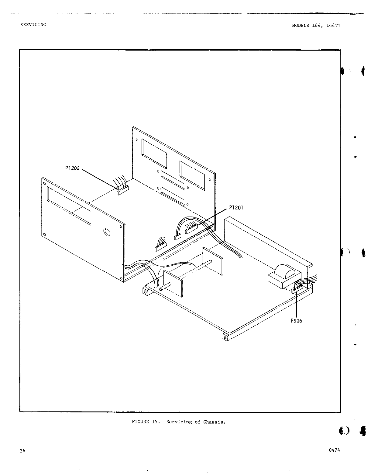
b. Chassis *ssembly. To gain access to the remaining printed circuit boards the following procedure should be used.
Remove the front pane1 Range knob assembly
1.
as shown in Figure 14. Loosen the 070 set screws
hoiding the switch coupler to the switch shaft
using a l/16 hex size (Allen Head) screw driver.
mgure 13 shows the proper orientation of the
Range knob for reassembly.
2. Remove the front panel Allen Head screws
in two places as shown in Figure 14 using a 3132
hex size screw driver.
Remove the rear panel Phillips head screws
1.
in two places as shown in Figure 14.
4. remove connector 5906 which is wired between
PC-254 and PC- 348. Replace conneceor with longer
jumper cable (furnished in the Node1 1603 Extender
Card Kit) which "ill apply power to the instru"enr.
5. Separate the circuit board assembly from the
chassis as sharrn in Figure 15.
whenever rez5istance checks are
1. Remove the two Phillips head screws from
the underside of PC-254 as shown in Figure 16.
Remove the slotted screw and "UC holding
2.
PC-248 and E-250.
Remove the long slotted screw and fastener
3.
as show" in Figure 16.
4. Remove the two standoffs holding PC-248
and K-250.
5. Remove circuit board PC-255 and replace
with ~xfender Card 24681C (from Model 1603
Extender Card Kit).
CAI.IBRATION CONTROLS
5-5.
a. Offset Currene Adjust (R733). This control
is a screw driver adjustment accessible from the
bottom cover as shown in Figure 18.
b. Ohms Cal Adiuse (R738). This control is a
screw driver adjustment accessible from the boft"m
cover as shown in Figure 18.
DC valance Adjust (R722). This control is
C.
an adjustment accessible from the bottom cover as
show" in Figure 18.
screw driver zo avoid contacting the chassis.
15" ~dj. (~209). This control is located on
d.
R-254. Remove rhe top cover ior access to the
CO"t~Ol.
e. CLOCK Ad,. (R605L. This control is located
on PC-254. Remove the tap cover for access.
1". IO", loo", 1000" Controls (lull, R108,
f.
~106, R104). These controls are also located on
R-254.
B. i-CAL, -CAL Adlust.
on K-250.
COMPONENT LAYOUTS Am OUTLINE DRAWINGS.
5-6.
Caution! Use an insulated
These controls are located
4,
s
w
!
v
C. Printed Circuit Board Installation. The loca-
tion of all circuit boards is shave in Figure 16.
TO gain access to circuit boards PC-248, PC-250, and
PC-255 the following procedure should be used.
24
a. COmpOnent Layouts. The component layouts iden-
tify all parts on the printed circuit boards using
circuit designations from the schematic diagrams.
4.1
0474
a
Page 30

SET SCREW
tgfii &jf$G
SET SCREW
1s:
"
STEP 1.
1OOOV POSITION
I
,t+ ‘;
STEP 2.
1mV POSITION
FIGURE 13. RANGE Knob Assembly.
12
d
SCREW
FRONT PANEL,
2582 C
KNOB, KN-33
SWITCH COUPLER, 24583A
Page 31
I
26
0474
Page 32

MODELS 164, 164~1
SERVICING
0474
27
Page 33

PC-254
MODELS 164. 164~7
P1209 P1201
Page 34

MODELS 164. 164~~
SERVICING
Xlerload Indication when
.nput ia shorted.
,I . II
I, II
Trouble-Shooting Procedure
Probable Cause
power failure
210" supply failure Check 21OV supply voltage on PC-254. If low, check
Line switch set at 234V
with 117" line input.
Analog amplif$er ""f of Check integrated circuit QA703 on analog board PC-251.
balance.
Transistors Q402 and Q403
Oscillator Circuit (Clack) Check CLOCK frequency at CLOCK test point. Frequency
TABLE 5-2.
SOl"tiO"
Check fuse.
(broke" wire, loose hardware, etc.).
by removing top cover and unsoldering pig-tail fuse.
rectifier diode D206.
NO. RF-l,.
Sef switch t" 117".
Replace with Kelrhley Part NO. IC-2.
mains, check MOS PET transistor Q701 and ~702.
with Keithley Part Na. 'E-51.
NOTE: These transistors are sensitive t" static charges
Therefore, drain static charge from hands and/or tools
using a foil grounding surface. Disconnecr the solder-
ing iron from power before using.
Check for zer" voltage level on pin 6 of integrated
circuit Q.4401. If not ac zero, replace cransistars
with Keithley Part No. 'E-71.
should be 10kHz 220 Ha.
brace as in Section 6.
check transistors 4601, 4602, and Q603. Replace with
Keithley Part NO. 'E-62.
If blow", check for a" internal short
Replace fuse
Replace with Keithely Part
If difficulty re-
If ""t of tolerance, recali-
If clock frequency is missing,
Replace
hs ranges inaccurate.
:vo1tage ranges are
lO-1)
ohm* reference amplifier
-
:urrenr reading inaccurate Shunt resistor out of
c
I" one range only
c
hrerrange "1" not lighted Tra"8isfOr Q301 or inte- Replace transistor Q301 if shorted from collector co
c
rhe" if should indicate.
.a
hrerrange "1" lighted con- Transistor Q301 or ince-
c
,iruously "he" it should grated circuit QA301.
t
'ot indicate.
”
P
'olarity signs remain
1
.igheed or do "at light
a
It all.
c
ligifal Readours incorrect. Decoder driver circuit
0474
tOl&-a"Ce. siseors R116 through R122.
grated circuit QA301. emitter (Keithley Part No. TG-67). Ocherwise. replace
Transistors Q305 and Q306.
Integrated circuit Q.4305.
Decade C"unter circuir
Buffer Storage circuit
Check integrated circuie QA704.
NOTE:
age applied in ohms mode.
Part No. Z-2. Also replace resistor R745 with Keith&y
Part No. Rl68-UK. Recalibrate ems circuit. Select
R739 as necessary.
Replace shunt resistor for that particular range. Ke-
QA301 with Keithley Part No. X-9.
Replace as above.
Replace tra"sisf"rs Q305 and Q306 with Keithley Part NO.
W-67.
Replace either QA314, QA315. or QA316 with Keichley
Part No. X-3. (These integrated circuits are "of
saldered because of plug-in sockets.)
Replace either QA308, QA309, or QA31O with Keithley Part
NO. x-17
Replace either QA311, QA312. or QA313 with Keiehley Part
No. IC-16.
Integrated circuit may have failed due to volt-
Replace QA704 with Keifhley
Replace QA305 with Keithley No. IC-7.
21
Page 35

SECTION 6.
CALIBRATION
6-1. GENERAL. This section conrains procedures for
checking the instrument to verify operation within
specifications.
TEST EQUIPMENT. Use test equipment recommended
6-2.
in Table 6-1 far accuracy verificafion.
6-3. PROCEDURES.
Preliminary.
a.
1. Warn-up Period. WiLh Power Switch ON, allow
the instrument fo warm-up far a minimum of 30 min-
utes.
2. Power Supply Checkout. All the power supply
voltaees can be measured at test points on minted
circuit board PC-254 as shown in &gure 18.'
TABLE 6-1.
Test F.quipmenr
6-2.
TABLE
lr supp: Ly Voltages
Tesf
Point
+15.00" dc
-15.0" dc
+3.6" dc
+21ov dc +21ov
-~170" dc +17ov
b. Adjustments.
1. Power Supply. The +15V supply should be adjusted foe +15.OOV dc kO.0507 using potentiometer
R209 on PC-254 as shown in Fiwre 18. The -15"
and f3.6" supplies cannot be adjusted since the
f15V supply is used as a reference voltage.
+15v
-15"
+3.6V
+14.95 to +15.05
-14.6 to -15.4
+3.4 to +3.*
f205 to +230
+I65 to +I75
+
*
CO&
Letter
A Voltmeter, Digital ilLI" to ~1000" YJ.l% Keithley, Model 160 Zero Adjustment
B
C
D Resistance Box
E current source
Inserument Type Specification and Model No. Use
of reading
Voltmeter, Differential
Voltage Source
limit of error 20.01%
of reading or 1OpV
.003% voltage mode
10, 100, 1000 vo1rs Voltage Source
2.02% aCC"raCy
10 megohms maximum Type 1433
.006% accuracy
0.1 In4 to 100 mA Current Source
.003% voltage made Fluke, Model 333OB
.02% resistance
accuracy
Manufacturer
Keithley, Model 662
Fluke, Model 3330B
ES1 type SR-1010
Divider Rafio
General Radio
Decade Resistor
Fluke, Model 3330B
Voltage Source (l.OlV)
General Radio
Type 1433
Decade Resistor
"*lfage Calibration
Current Calibration
Resistance Calibration
Voltage Calibration
10, 100, 1000 volts
.OOl, .Ol,
Resistance and
Current Calibration
Current Calibration
O.lmA to lOomA ranges
Current Calibratian
.OOl to .OlmA ranges
.l, 1 volts
Page 36

I
MODELS 164, 164TT
CALIBRATION
2. CJ~“Ck Frequency. Measure the clock frequency
aL Lh.2 "C,.OCK" test point 0" PC-254 as show" in
FiglllE 16.
II nomi,nai iOkH2,
an PC-254 as shorn in Figure 18.
4. 'The output should be adjusted to zero within
Ll millivolt.
5. Ioc Balance. With voltmeter (A) connected to
the "UTPU'l adjust the OFFSET CURRENT MJ. Control
(R733) for zero an the 1V range.
be adjusted within tl millivolr on the 1mV range
and within 10.1 millivalr on the 1V range.
che adjustments of R505 and R733 until the OUTPUT
is within tolerance on both the 1mV and 1V ranges
simultaneously.
1f the OUTPUT cannot be adjusted t" within
zlmv on the lmv range place B jumper between
input low and the junction of P.503 and C504 on
K-254.
ndjust: oc bal.ance pot R722 (on PC-251~) for
zero at the OUTPUT.
ii,,<, repent steps 4 and 5.
3,~~ ,>roperly set, replace 31209 on PC-348 and
adust front panel zero RI215 for flashin
~!'he frequency should be adjusted lor
120 Hz using porentiomeeer K605
The OUTPUT should
Repeat
NOTE
Theo set RANGE switch LO 1OOmV and
Remove jumper irom R5O3
After R505 and 11733
6. Analog Calibration.
a).
the analog OUTPUT.
to the Input Terminals (red and black). Measure
the analog OUTPUT voltage for each range as described in 'Table 6-3.
lm" ranges wire jumpers are "set, for caiibrotion.
On the lV, 10". lOOV, and lOOOV ranges potentiometers Rlll, R108, R106. and H104 should be
adjusted.
cecr decade rssiscance box (D) to the Input Ter-
minals.
as described in Table 6-4. Adjust the OHMS CAL
potentiometer (R738) for an OUTPUT of +1V rl.O
millivolt on the lkn range only. The remaining
resistance ranges cannot be adjusted.
current source (E) to the Input Terminals.
sure rha analog OUTPUT for each current range as
described in Table 6-5. No calibration adjustments can be made an any of the current ranges.
7.
Input Terminals. Adjust the front-panel ZERO Control so chai the Digital Display reading is O-O-O0 on the lm" r*n$y with the Fol.,rity 1niiicacnr al-
ternating plus anti minus. Llensure the analoe OUT-
PUT volcagc which shoul~d be within $1 miili~olt of
"alrage Rmges. connecr va1rmeccr (8, to
b). Resistance Ranges (Model 160 only). Con-
Measure the analag OUTPUT for each range
Current Ranges (Model 160 only). Connect
C).
Digital Calibration.
Zero Check.
a).
connect ""lug= *D"rCe CC)
On the iOh", lOm", and
Hea-
connect a shorting wire *crc'*s
Page 37

c‘uIBP.ATIOM
MODELS 164. 164TT
Full-Scale Indication. Connect voltage
b).
source (0 to the Input Terminals and adjust the
source for +1.9992V measured at the analog OUTPUT.
Adjust the -CAL Control (R402) 8" that the Digital
Display has a reading which altarnatas berveen
l-9-9-9 and a blanked display (with only the overrange "1" lighted)
adjust the +CAI, Co&l (R408).
Linearity Mju.ement. COIUI*C~ an ae~urata
C).
voltage source (C) to the Input Terminals and adjust for an analog OU'ITUT bf +0.9992V on the 1V
range. Verify that the Digital Display reading
ia O-9-9-9. ,Resdjnst the voltage so"rca for an
analog OUTPUT of tO.9998V~on the 1V ranga. Verify
a change of the Digital Maplay from O-9-9-9 to
1-O-o-o.
Apply a negative input and
8. Calibrstion af Milliahm Current Source.
Warm-up period.
a).
allow the instrument to warm-up for a minimum
of 30 minutes.
Connect resistance box to inputs "sing
b).
four lead wires -- two connected to ti SOURCE
(current leads) and two connected to HI and
LO (voltage leads).
Set R box to zero resistance and read
c) .
residual resistance "itb 164. Set R box to
10.000 ohms including residual. Adjust 81203
for reading of 10.00 in Operate position after
zeroing out thermal Wp's in zero position.
With Power Switch ON,
A
F
32
FIWRE 19.
.t
V
Calibration Controls.
Page 38

TABLE b-4.
Range Input source
SeCtf”g source Accuracy
ltm us
100 0 100 n 1.02%
lOKn
lOOK
um lm 02%
lOMR 1oMn ?.4%
lmmi loom
1OOOMn lOOOtm *35:
1oKn
loom ?.OZ%
O.lpA
W
lO”A
lOOvA
lmA
lOmA
lOOmA
lOOh
lOOhA
01%
?.02%
kl%
current Range Calibration
I”PUC
.%“PX Accuracv
O.lPA 02% 1.000”
1lrA
lOPA
1OOuA 02%
InA
lomA 02% 1.000"
lOomA 02%
1oocmA
lOhA
An.¶log
OUTPUT
“Olt.%ge
1.000”
1.000”
1.000”
1.000”
1.000”
1.000”
1.000”
1.000”
TABLE b-5.
source OUTPUT OUTPUT
f.02% 1.000"
f.OZ% 1.000" f 2nl"
+.02x 1.000” t 2mv
02% 1.000" ? k"
f.02% 0.100" i-0.h"
Analog
OUTPUT
Accuracy
2 llr”
f lm”
t 4rtl"
t h"
t 3rd
A 4om"
flOOV2"
~5Oom"
Analog Analog
“alta.9.e ACCUr.Xy
1.000" t 2s
1.000" ? 3rn"
Ref.
oesig.
R738
____
_--____
_______--_
____
t 2mv
t 2m"
i 2rn"
33
Page 39

MODELS 164, 164TT
34
R1203
,m SOURCE
FIGURE 20. Calibfatio” of Milliohm current source.
0474
Page 40

SECTION 7.
REPLACEABLE PARTS
# c;“ded.
I ’
7-1. REPLACEABLE PARTS LIST.
a list of components used in this insfrument for user
reference.
individual parts giving Circuit Designation, Descripfro”, Suggested Manufacturer (Code Number), Man”fac-
A
CbVar
I
cerrl
cer Trimmer
camp
DCb
msig.
PAL
ETB
ETT
The Replaceable Parts List describes the
ampere
Deposited Carbon
DeSignafio”
Electrolytic, Aluminum
Electrolytic. Tubular
Electrolytic, tantalum
I.
7-2. ELECTRICAL SCHmATICS AND DIAGRAMS.
and diagrams aie included to describe the electrical
circuits as described in Secrion 3. Refer to Table
7 2 which identifies all schematic part numbers in-
7-3. HOW TO USE THE REPLACEABLE PARTS LIST. This
Parts List is arranged such that the individual eypes
of components are listed in alphabetical order.
parts for the instrument’s Main Chassis are listed
followed by printed circuir boards and other subassemblies. Refer fo Table 7-3 for listing of circuit designation series assigned to each ma,or subassembly.
HOW TO ORDER PARTS
7-4.
This section contains
Abbreviations and Symbols
F
Fig. Figure
GCb Glaes enclosed Carbon
k kilo (103)
u
M leg (106)
Mfg.
MU Metal Film
MY
No. Number
schematics
The
TABLE 7-1.
farad
micro (10-b)
Manufacturer
Mylar
tllrer Part Number, and Keitbley Part Number. AlSO
included is a Figure Reference Number where qplicable. The complete name and address of the &mufacrurers is listed in ehe CODE-TO-NAME usting
following the parts list.
n ohm
:c
POlY Palystyrene
Ref. Reference
TC” Tinner Copperveld
V valt
w watt
WV
uwvar Wirewound Variable
pica (IO-=)
Printed circuit
Wirewound
a. ReplaceabJe parts may be ordered tbrnugh rbe
Sales service Department, Keirhley Instruments, 1°C.
or your nearest Keitbley representative.
b. When ordering parts, include the following in-
format*o”.
1. I”Str”me”t Part Number
2. I”Str”me”c Serial Number
3. earc Description
4. Schematic circuir Designacio”
5. Keithley Parr Number
C. All parts lisred are maintained in Keithley
spare Parts Stock. Any part not listed can be made
available upon request. Parts identified by the
Keitbley Manufacruring Code Number 80164 should
be ordered directly from Keithley Instruments, Inc.
0474
TABLE 7-2.
S”iLchi”g - Main Chassis Front Panel 262438
power
Supply
connectors
Analog Amplifier PC-251
Integrator Board PC-250 24690E
Tube Board
Tube
Board
Millfdrm source
Trip Circuit (Model 164TT) PC-348
Digital Output (Model 1602)
AC-DC Probe (Model 1601)
PC-254
K-254, PC-255 26246D
PC-248
PC-248 246890
PC-348
PC-287
__
262450
262448
246880
24642D
2622X1
246850
2466%
35
Page 41

REPLACEABLE PARTS
MODELS 164, 164TT
TABLE 7-3.
CirCUit
Desig. Deecripfio”
-- Main Chassis
PC-254 mwer supply __ 200 38-46
PC-248 Tube Board 5802 300 38-46
PC-250 lntegraror Board 5801 400 38-46
PC-254 Input Filter _- 500 38-46
PC-254 OSCillat”r -_ 600 38-46
PC-251 Analog Amplifier 5902 700 38-46
PC-255 connecrar bard 301 800 38-46
PC-254 connectors -- 900 38-46
PC-348
-
1) Fmnt Panel
2) Rear Panel
To,, Coyer Assembly
3) cover, Sheer Metal
4) Screws, 116 x 318 slotted. pan head 4 _-_
Handle Assembly
mn source, Dual Trip8
Mechanical Parts l.isc
Description
connecear Page
Pl”g-I” series NO.
--
__
TABLE 7-4.
quantity Keifhley
Per kssembly Part NO.
1
1
_--
1 26021D
.
100 M-46
1200,1300
25827C
25828C
26028B
___
Y-46.47
\,:
I
36
5) Handle 1
6) Screws #b-32 x 318" R. H. Slotted 2
Bottom Assembly --- 260298
7) aotfom
8) Fastener
Feet Assembly
9) Feet 4 24322B
10) *alI
11) Screw. 06 x 7116" Phillips. Flat Head 4
Tilt Bail Assembly
12) Bail 1 l.7147B
13) Kep Nut 4 ---
1
2
_-_ -_
4 FE-b
_-_ _-_
HH-18
26024C
FA-54
-__
0474
Page 42

4) SCREW
5) HANDLE
1) FRONT PANEL
FIGURE 21. Top cover Assembly.
FIGURE 22.
Bottom cover Assembly.
12) TILT BAJL
0474
37
Page 43

REPLACEABI.E PARTS
MODELS 164. 164TT
Models 164, 164TT. (See schematics 262433, 26245D.
262460, 26244E, 24690'S, 24688D, 24689D. 246421)).
CAPACITORS
circuit
msig.
Cl01
Cl02
Cl03
c201
c202
c203
C204
C205
C2Ob
C207
C208
c209
C210
c211
c212
C301
c302
c303
c304
c401
C402
c403
c404
c405
C406
c407
C408
c409
C410
c411
C412
c413
C414
c415
C41b
lx17
C418
c419
C420
.0047pF, soov, CerD. .
.0047llF, SOO", CerD. .
.0047@, SOO", tea. .
2OOO!lF. IS", FAL . . .
220PF, 1000", cerll .
150pF. 1000", cerJJ .
ZOOuF, 35". EAL. . .
ZOO"F, 35". SAL. . .
10°F. 20". ETT . . . .
47&F, iooov, cerll . .
125lrF. 15", ETB. . . .
200uF. 35”. EAL. . . .
ZOO"F, 35", EAL. . . .
125°F. 15", ETB. . .
15uF, 300", EAL. . . .
.0022"F, SOO", cem. .
lOOPF, lOOOV, CerD . .
0.2&F, IO", ETT . . .
lOPF, 1000", certl. .
10PF. 1000", CerD.
lOPF, 1000", cercl. . .
100°F. 1000". &I-D . .
lO~F.'20V, ETT . . . .
1.5pF. boo", CerD. .
1°F. 100". MY. . .
.OOl,,F, lOOOi, CerD. .
Not Ueed . . . . . .
ZZOPF, 1000", CerD
lO,,F, ZO", ETT . .
lOuF, 20". ETT . . .
22pF, lo", ETT .
5DF. 1000". CerD . .
1;F: 50". &F .
.0047"F, SOO", Cm-D.
390PF, lOOOV, cem .
10uF. 20". ETT . . .
O.luF. 250". MtP . .
10°F. ZO", ETT . . .
lop, zov, ETT .
. .
. .
.
. .
. .
. .
Mfr. Mfr. Keifhley
Code Desig.
. .
. .
. .
. .
. .
. .
. .
. .
.
.
.
.
.
. .
. .
. .
. .
. .
.
. .
. .
. .
. .
. .
. .
. .
. .
. .
. .
.
.
.
. .
. .
.
. .
.
. .
.
. .
. .
. .
. .
. .
. .
. .
.
. .
. .
. .
.
.
. .
.
.
.
. .
. .
.
. .
. .
. .
.
. .
.
. .
.
. .
.
. .
. .
. .
. .
. .
.
. .
. .
. .
. .
. .
. .
.
. .
. .
. .
. .
. .
. .
. .
. .
. .
72982 801-ZSUO-472M C22-.0047M
72982 801-Z5UO-472M C22-.0047M
72982 801-ZSUO-472M C22S.0047"
29309
71590
71590
90201
90201
17554
71590
73445
90201
90201
73445
90201
72982
71590
17554
71590
71590
71590
71590
17554
71590
. . . . .
71590
17554
17554
17554
71590
72982
72982
71590
17554
367502001X
DE-221
m-151
"TVZOON35
"TVZOON35
mm-20
m-471
C426-125°F
MT"ZOON35
C426-125,,F
PTC015M300
831-ZSUO-222M CZZ-.0022M
DD-101 C64-1OOP
TSD210226 C180-0.22"
DE-100 C64-1OP
m-100 C64-1OP
m-100 C64-1OP
DD-101 C64-1OOP
TSD1-20 c179-1OM
TCZ-15 C?,-1.5P
MF825 C185-IN
808-OOO-Z5R0102K C64-.001M
. . . . . .
DE-221
mm-20
mm-20
TSDZ-lo
m-050
8131050651105M C23?-lM
801-ZSUO-472M CZZ-.0047M
m-391 Cb4-39OP
TSD1-20
. .
. .
. .
.
.
17554
17554
Part NO.
t .
. .
.
C93-ZOOOM
C64-220P
C64-15OP
Cl,,-200M
Cl??-2OOM
Cl?%1OM
Cb4-470P 1
C3-125" 2
Cl?,-ZOOM
Cl?,-200"
C3-125M
C173-15M
. . . . . . . .
C64-220P
C179-10M
C1?9-10M
cmo-22M
C64-5P
C179-10"
C178-.lM
c179-1oM
c179-1OM
11 *
. . .
. .
7’
I
.
1
2
2
1
3
1
1
3
.
c501 O.l"P, zoov, My. . .
C502
C503 Z,,F. 100". My. . .
C601 .047uP, zoov, My . . . . . . .
C602 SOOpF, SOOV, Silver Mica . . . .
Cb03 SOOpF, SOOV. Silver Mica . . . .
C604
C605 lOuF, zov, ETT . . . . . . . . .
c701
C702
c703
c704
c705
C7Ob
38
O.l$, zoov, My. . .
1500PF, soov, Silver Mica. . . .
Nat Used ............
O.OluP, ZO"", My ........
10°F. 2ov. El-l .........
o.boi7uP,'500v, C&-D ......
l.ZuF, 2OP, ETT. ........
l.ZuF, ZOV, ETT. ........
. .
. .
. .
. .
.
. .
. .
. .
. .
. .
. .
. .
. .
. .
. .
. .
. .
. .
. .
. . .
. .
. .
. .
. .
. .
. .
. .
. .
. .
. .
. .
. .
. .
. .
13050
13050
14655
14655
14655
17554
. . . . .
13050 SML+.Ol”F
17554 TSD1-20-1O~F
72982
17554 TSDl-ZO-1.2pF
17554 TSDl-ZO-1.2uF
?.M2A-.047pF
CD19FD501P03
cD19FD501F03
CD19FD152P03
TSrJl-20
. ...*..
801-zsuc-472M
c143-.l.M
c143-.lM
Cl&+2M
C143-.047M
c209-5OOP
c209-SOOP
c209-15OOP
C179-1OM
. . . . . . . .
c47-.olM
c179-Km
C22-.0047M
c179-l.w
c179-1.2M
2
. .
1
1
2
. .
1
. .
1074
Page 44

MODELS 164, 164TT
CirCuit
msig.
Models 164, 164TT.
CAPACITORS (Cont'd)
Mfr. Mfr.
DescriPeio" Code Des@.
REPLACEABLE PARTS
Keithley
Part NO.
WY.
Cl07 O.O047LiF, 500", CerD. . . . . . . .
Cl08 220pF, 1000", cerl?. . . . ,
3
Cl09 O.lpF, 25OV, MtF. . . . , .
Cl10
c711
C801
Cl201
Cl202 0.0022$, 500", CerD. . . . . . . . 72982 831ZSUO-222M
Cl203 O.OlllF, sov, My . . . . . . . . . 84411 601X?-.01$
circuit
DesiF,.
D201 Rectifier ...................... 13327
D202
0203 Full Wave Bridge Rectifier. .............
0204 Rectifier ...................... 01295
D205 Rectifier ...................... 01295 lN645
D206 Rectifier
0401
D402
0403
0404
D405
D406
D407
$EL!
D410
0411
D412
0413
0414
D415
0416
0417
0.22@, 25OV, MtF . . . . . , .
O.l#F, ZSOV, MLF. . . . . . . . .
O.OOluF, lOOOV, certl. . . . . . .
470,,F, 40", F.AL . . . . .
Rectifier ...................... 13327 IN4139
......................
zener, 9", 1/2w ...................
zener, 9", 1/2w
Transistor. Base-Emiteer NPN, Case TW106
Transisfor, Base-Emitter NPN, Case TO-106
Rectifier ...................... 01295 lN914
Rectifier ...................... 01295 IN914 RF-28
Rectifier ...................... 01295 IN914 W-28
Rectifier ...................... 01295 IN914
Rectifier ...................... 01295 lN914 RF-28
Rectifier ...................... 01295 lN914
zener, 9.1v ..................... 06751
Rectifier ...................... 01295
rectifier ...................... 01295
Recfifyr ...................... 01295 IN914 RF-28
Rectifier ...................... 01295 lN914 RF-28
Rectifier ...................... 01295 IN914 RF-28
Rectifier ...................... 01295 lN914 RF-28
................... 04713 lN936 m-5
......
......
72982 801-ZSUO-472M
71590
73445 C280AE-.111F
73445 C280A&.22"F
73445 C28OAE-,luF
72982 808000-ZSRO-102K Cb4-.OOU,
Amperex ET471X040A2
83701 PD-10
01295 lN3255
04713
07263 2~3565 n-39
07263 2N3565
m-221
lN4139
lNb45
113936 DZ-5
lN713A DZ-38
lN914
lN914
C22-.0047M
Cb4-220P
C178-.l"
C178-.22M
C178-.lM
ClSO-47OM 1
c22-.0022"
c41-.om
RF-34
RF-34
U-36
RF-14
RF-14
m-22
s-39
RF-28
RF-z*
RF-28
RF-28
RF-28
13
1
1
1
2
2
8
2
1
D501 Rectifier ......................
D502 Rectifier ...................... 01295
0601
D701 Rectifier ...................... 01295 IN645
D702
Dl201 Bridge Rectifiex, 2A. 100 PI" ............ . . PDlO RF-36
D1202
D1203 Zener, 6.2V. 0.4W .................. 06751 1N823 LIZ-36
D1204
D1205
D1206
Dee&.
s301
3
0474
Rectifier ......................
zener, 9". 1/2w ................... 04713 IN936
Zener, b.Z'?, 0.4W .....
Rectifier ......................
Rectifier ......................
Rectifier ......................
DeSCriPti””
Lamp. (OVFXUNGE)..................
.'
............ 06751 lN823 DZ-36
01295
01295
01295 lN645
01295 lN645 RF-14
01295 lN645
Mfr. Keithley
Code rlesig.
80164 PL-42 PL-42 1
113645
lNb45
lN914
RF-14
RF-14
RF-28
m-14
DZ-5
RF-14
Fe-14
Part NO.
.
. .
2
.
. .
. .
Qty
39
Page 45

OS302
Lamp, (POLARITY). . . . . . . .
80164 IX-48
K-48
F201
I?202*
*AlteTTlate
5102
5103
5104
JZOl
3202
.I203
5204
5205
3801
J8o2
JVOl
5902
5903
5904
3905
5906
JlZOl
51202
51203
51204
.n*os
51206
.I1207
51208
.a!09
51210
Fuse, 1/4A, 250", 3.G. Slo-BlO. . . . . . .
Fuse, l/2& 125", 3b.G. Sl0-no. . .
CCJNNECTORS
Binding Post, (HI) Red.
Binding POSC (LO) Black
Connector, *alag OUCP”L.
Binding Post, (CASE) Green.
Connector, Female, Berg
Connector, s-pin. ..................
Test Poinf. .....................
Test Point. .....................
Test hint. .....................
Connector, 22-pin, card-edge type
connector, 44-pin, card-edge type
Ca""ector, 22-pin, card-edge type
connector, 22-pin, card-edge type
Receptacle, lo-pin.
Receptacle, lo-pin.
Receptacle, lo-pin.
Receptacle, lo-pin.
Housing, lo-pin ...................
Housing, s-pin. ...................
Binding Post, (LO), Black
Binding Post, (HI), Red
Housing, *-pin. ...................
Housing, s-pin. ...................
*erg Pill, Female. ..................
Housing, 35pin. ...................
Housing, Spin. ...................
Housing, 3-pin. ...................
...............
...............
..............
.............
...............
..........
..........
..........
..........
.................
.................
.................
.................
..............
...............
71400 MY+1I4A
75915
58474
58474
02660
58474
22526
09922 PSC4SS2212
09922 PSC4DD2212
09922
09922
22526
22526
22526
22526
22526
22526
58474 DP2lBC
58474 DF21RC
22526 20370
22526 65039034
22526
22526 65039034
315-500
ImlRC
OF21BC
aoxm
DFZlGC
20052
PSC4SS2212
PSC4SS2212
20052
20052
20052
20052
20052
20370
65039034
m-33
Iv-35
BP-11R
BP-lx3
CS-32
BP-11c
CS-237
CS-182
c-205
CS-182
m-182
CS-237
lx-237
CS-237
CS-237
CS-237
m-251
BPllBLK
BPllR
B-261
cs-251
CS-270
B-270
CS-270
1
P201
P1201
P1202
P1203
PI204
P1205
PI206
P1207
PI208
P12O9
q201
qzo2
0203
Q204
40
Receptacle, 3-pin, Line Voltage
Berg Pins (10). ...................
Berg Pins (5) ....................
Not Used. ......................
Not Used. ......................
Berg Pills (2) ....................
aerg Pins (5) ....................
aerg Pin (1). ....................
Ierg Pill.9 (3) ....................
aerg Pins (3) ....................
power, NPN, case m-66.
NPN, case TO-104. ..................
NPN, case 1'0-106. ..................
NPN, Case 'E-106. ..................
............... 02735
...........
82389 wLC3OL
80164
80164
. . . . .
.
80164
80164
80164
80164
80164
Code
02734 285183
07363
07263
.......
.......
Mfr.
Deeig.
40312
283565 K-39
2N3565 x-39
CS-254
24249A
24249A
. . . .
. . . .
24249A
24249A
24249A
242498
24249A
mithley
Pare NO.
m-54 1
x-68
t .
1074
1
2
Page 46

MODELS 164, 164TT
4205
q206
q207
Q208
a209
6210
6211
q212
PNP, case RHO. . .
NPN, case TO-5. . .
PNP, case RllO.
NPN, case TO-5.
PNP, case RllO. .
PNP, case RllO. . .
PNP, case KllO.
PNP, case RllO.
. .
. .
.
Models 164, 164TT.
TRANSISTORS (Conr'd)
Mfr.
Code
.
.
07263
02734 40317
07263 S17638
02734 40319
07263 S17638
07263
07263 517638
07263
Mfr. Keithley
Lxsig. Parr No.
-
S17638
S17638
S17638
-
qty.
TC33
x-43 2
x-33
n-50
x-33
n-33
x-33
v-33
6
1
Q301
6303
9304
Q305
Q306
Q401
Q402
0403
6404
6405
q406
Q407
4408
q409
q410
q411
q412
0413
q414
q415
Q416
q601
4602 NPN, case To-92 ......
Q603
q701
Q702
0703
4704
q705
Q706
Q707
Q708
NPN. case TO-104. .
NPN, case m-5.
NPN, case TO-S. .
NPN, Case TO-106. .
NPN, case m-104.
NPN, case w-104. .
N-man, Pet
FET. case TO-92
FET, case TO-92
Pm', Case 'W-106.
NPN, Case 'TO-106.
NOf Used. .
Not Used. . . .
N-man, PET . .
PNP, Cake TO-106.
NPN, Case TO-106.
N-cilan, PET . .
NPN, Case 'W-106.
PNP, Case W-106.
NPN, Case 'E-106.
PNP, Case TO-106.
NPN, Case 'E-106.
NW, case To-92 ......
NPN, case To-92 ......
N-Ghan PET (Selected*). ..
N-Ghan FET (Selected*). ..
NPN, Case TO-92 (Selected*)
PNP, case m-92 ......
N-man PET. ........
NPN, case Tc-92 ......
NPN, case m-92 ......
PNP, case TO-92 ......
.
. .
.
.
. .
. .
. .
. .
. .
*
.
.
. .
. .
. .
.
.
.
. .
. .
. .
. .
. .
.
.
.
. .
.
. . .
07263 2N5184 'R-67
02735
02735
07263 2N5134 X-65
07263 2N5184 R-67
07263
04713 284220
01295 TlS70
01295 TlS70
07263 2N5139
07263 2N5134
. .
. . . . .
04713 2N4220
07263 2N5139
07263 2N5134
04713
07263
07263 2N5139
07263 2N5134
07263 2N5139
07263 2N5134
04713 2N5089
04713 285089
04713
94145 RN1030
94145
04713
04713 2135087
04713 MPF-103
04713
04713
04713 2N5087
40346 x-44
40346 E-44
2N5184
. . . .
. .
2N4220
2N5134
2N5089 TG-62 .
RN1030
2N5089*
2N5089
2N5089
E-67
X-42
TG-71
TC-71
TC-66
X-65,
. . . . . .
. . . . .
x-42
E-66 .
E-65
n-42
'K-65
X-66 .
'X-65 .
T&66 .
'K-65
E-62 6
E-62
m-51 (24598A)* *
m-51 (2459&h)*
E-62 (24219A,*
X-61
TC-41
E-62
Z-62 .
E-61
3
*
6
4
2
3
.
2
1
Q1201
0esiFx.
QA201 Regulator. 10-p** case TO-100 ............ 07263
QA301 Dual J-K Flip-Flop, 14-pin DIP. ........... 04713
qA302
QA303 quad Z-input NOR, 14-pin DIP. ............
QA304
QA305
QA306
QA307
QA308 0ecade counter, 14-pin DIP. ............. 04713
QA309 Decade counter, 14-pin DIP. .............
0474
Transistor. ........
Descripflon Code walk?.
Dual J-K Flip-Flop, 14-pin DIP. ........... 04713 MC891P
quad z-input NOR, 14-pin DIP. ............ 04713
Hex 1rwercers, 14-pin DIP .............. 04713
Dual J-K Flip-Flop, 14-pin DIP. ........... 04713
Dual J-K Flip-Flap, 14-pin DIP. ........... 04713
. .
07263
04713 MC824P
04713
40317
Mr.
"5R772-339
MC891P
MC824P
"C889P
"C891P
"C891P
MCSSOP
MCSSOP
x-43
Keithley
Parr NO.
IC-14 1
K-9 4
IC-9 ..
IC-5 3
K-5
K-7 1
IC-9
K-9
x-17 3
IC-17 ..
qty.
..
..
..
41
Page 47
REPLACEABLE PARTS
MODELS 164, 164TT
Models 164, 164l"r.
INTEGRATED ClRCUITS (Cant'd)
Mfr. Mfr.
Description Code Dzsig. Part NO.
Keithley
QCY.
Q&310 Decade Counter, 14-pin DIP . .
QA311
qA312 quad Latch, 16-pin DIP . . . . . .
Q.4313
4.4314
QA3l5
4‘4316
Q.4401
QA402
QA403
QA404
QA701
q*702
QA703
q.4704
qA801 n*nary counter, 14-pin DIP .
QA1201
q‘4120*
RI.01
R102
RIO3
RIO4
xl05
RlO6
El07
RI.08
RIO9
RllO
Rlll
Rl12
RI13
Ill14
xl15
RLL6
m17
Rl18
Ill19
Kl20
PJ21
Rlzz
Rl23
Quad Latch, 16-pin DIP . . . .
Quad Latch, 16-pin DIP . . .
Decoder/driver, 16-pin DIP . . .
Decoder/driver, 16-pin DIP . , . .
Decoder/driver, 16-pin DIP . , .
Amplifier, &pin, Case TO-99 .
hlplifier, 5%pin, case To-99 ‘ .
Diff. Comparaear, +pin, Case TO-99. .
@lad z-input, NAND, 14-pin DIP .
Dual J-K Flip-Flop, lb-pin DIP .
Amplifier, *-pin, case To-99 .
Amplifier. a-pin, Case To-99
Amplifier, a-pin, Case TO-99
Regulator, case TO-220 . .
Amplifier, B-pin, Case 'E-99 . . .
lOMn, 1%. l/ZW. MLF. .................
*ookn, l%, l/ZW, MtF .................
lk.0, 0.1%. l/ZW, MtP .................
5on, 20x, zw, ww ...................
lOkn, 0.1%. 1/2w, MU. ................
soon, 20%. 2w. ww. ..................
lOOkt7, 0.1%. l/ZW, MtP ................
51in.20%.2W.ww ...................
lNn, 0.1%. l/ZW, MeF .................
lOOk0, 1%. uaw, MU .................
5okQ, 20%, 1.75w. cermec
107n, 1%. lW, DCb. ...........................
1090, 20%. 1/2w, Camp.
108~1, 1%. 2w, DC~. ..............
Ml. 0.1%. uzw, MCF
look,,, 0.1%. l/ZW, MfF .......................
lOkn, 0.1X, l/ZW, WtF.
lkn. 0.1%. l/ZW, MfF .............................
99.9*, 0.1%. l/ZW. MfP ................
0.1n, 0.1%. 5w, ww ..................
1n, 0.1%. 1/4w, ww
1on, 0.1%. lf4W. ww. ...........................
22on. 10x, 1/4w, Camp. ................
: : : : ............
.......
.......
.......
.......
.......
.......
.......
.......
........
.......
........
.......
.......
.......
.......
. . .
.......
.......
RESISTORS
: : :
: : : : :
: : : :
: :
04713
04713
04713
07263
07263
07263 “GS996079X
07263
07263
07263
04713
04713
07263
12040
12040
04713 MC-877P
04713 MC7815CP
12040 LH308"
07716
07716
91637
71450
91637
71450
91637
71450
91637
07716
73138
91637
75042
91637
91637
91637
91637
91637
91637
02985
01686
01686
01121
MC88OP
MC867P
MC867P
MC867P
"GB996079X
"GB996079X
“58770939K
“5B770939X
“5B771039X
MCSZPP
MC89OP
"58770939X
LM301AB
LM3OU.N
Mfr. Keithley
MEH-ZOOKD
Mm-1wI
lNS-115-500
HTFP-1OK
DC-I-10'n
GBT-10811
DC-2-108n
Miv-lm
MPP-lOOKa
MS-1OKG
Mm-1w
MFF-99.9n
TS-SW-.ln
7009-X
7009-1on
CB-221-10X
XC-17
X-16
E-16
X-16
IC-3
n-3
x-3
IC-1
K-1
z-4
x-5
K-8
K-1
IC-2
E-2
IC-21
IC-96
IC-67
R170-lOM
R94-ZOOK
Rl69-1K
mso-50
Rl69-lOK
Rp50-500
U69-100K
RP50-5K
R169-1M
R88-100K
RP64-50K
Rl3-107
R37-109
Rl4-108
R169-1M .
U69-100K .
R169-10K . .
B.l69-1K . .
FU69-99.9 1
Kl67-.l
R95-1 1
R95-10 1
R76-220 1
*
. .
. .
3
. 04713
3
3
1
1
2
.
1
1
1
1
R201
R202
R203
R204
R205
R206
FL207
R209
R210
R2ll
I(212
42
6.8ksL 10%. 1/4W, Camp ................
o.zn, 10x, TC" ....................
lOkCi, l%, 1/8W, MtF.
2.49k0, 1%. 1/8W, MtF.
lkn, 10%. 1/4w, camp .................
30, 1%. l/ZW, DCb. ..................
1.8ki7, 10X, 1/4W, Camp ................
3.32k‘L l%, 1/8W, MtF. ................
lkn, 20%. zw, w-d
3.Olkn. l%, l/SW, McF. ................
15kIl, 10%. 1/4W, Camp. ................
7.5kn, l%. l/SW, MtP .................
...................
...................
: : : : : : :
01121
91637
07716
07716
01121
91637
01121
07716
71450
07716
01121
07716
CB-682-10X
cc+z-.2n
CEA-lOK-1%
cm-2.49K-1%
CB-102-10%
DCP-l/2-3n
m-182-10%
CEA-3.32K-1%
lNS-115-1K
CEA-3.OlG1%
CB-153-10X
cm-7.5K-1%
R76-6.8K
Rl51-0.2 1
R88-10K 3
ms-2.49K 1
R76-1K 5
R12-3 2
R76-1.RK 1
R88-3.32K 1
RPSO-1K
R88-3.01K 3
R76-15K
R&3-7.5K 8"
1
1
11,
0474
Page 48

MODELS 164. 164T-r
R213
R214
It215
R216
R217
R218
R219
R220
1on. 10%. l/ZW, Camp .
wdl, 10%. 1/4w, camp.
30, 1%. 1/2w, DCb. *
33w, 10%. 1/4w, CcmP.
33kn, 10%. 1/4w, Camp.
,.skn* 1%. l/SW, MfF .
82fl, 10%. 1/2W, Camp .
lm, lO%, 1/4w, Camp
Models 164, 164TT,
RESISTORS (Cont'd)
Keithley
Part No.
-
.
. .
.
01121
01121
91637
.
.
. .
. .
.
.
.
.
.
.
01121
0112.l
07716
01121
01121
ES-loo-10%
CS-x33-10%
DCF-l/2-3fl
CB-33s10%
CB-333-10%
CSA-7.5K-1%
EB-SZR-10%
CS-LOS-10%
Rl-10 1
R76-33K
RlZ-3
R76-33K
R,6-33K-10%
RSS-7.5K-1%
Kl-82
R76-It,
8
1
2
B
R301
R302
R303
R304
R305
R306
R.307
R308
R309
R310
R311
R312
R313
is314
R315
R401
R402
R403
R404
R405
R406
R407
R400
R409
R410
R411
R412
R413
R414
R415
R416
R417
R418
It419
R420
R421
R422
R423
R424
R425
R426
R427
R428
0429
R430
R431
R432
R433
R434
R435
R436
R437
R438
looks& 10%. lW, C0rnp .
l.wl, 10%. 1/4w, camp
3.3kn, 10%. 1/4w, Camp
1.5kn. 10%. 1/4w, Corn*
.
.
1.5kQ. IO%, 1/4w, Camp
1ookn. 101, l/ZW, Camp
47kn, 10%. 1/4w, camp.
.
Not Used . . .
80.6kn. l%, 1/2W, MU.
7.87kn, 1%. l/SW, MtF.
lkn, 10%. 1/4W, Camp
.
1.5kn, 10%. 1/4w, Camp
lOkn, l%, 1/2w, Me. .
1okn. 1%. uzw, MfF.
low, 1%. l/ZW, Mm. .
lOkn, 10%. 1/4w, Camp. . .
lOkn, 20%. Cermet. . . .
7.5kq 1%. l/SW, MU . . .
7.5kil. 1%. 1/8W. MtF . . .
7.5kn, 1%. l/SW, MtF . .
Selacted*O, 1%. 1/8W, MeF. .
lOhn, 10%. 1/4w, Camp. . .
lOM, 202, wrlnet.. . . . . .
7.5M, 1%. 1/8W, MfP . . .
7.5kJI, 1%. l/SW, Mm .
7.5kQ, I%, l/SW, MfF . . .
Selecred*O, 1%. 1/8W, MU.
49.9k*, 1%, l/SW. MtP. . . .
49.9kn. 1%. l/SW, Mm. .
lOOkI& 10x, 1/4w, Camp . .
lOOk& 10%. 1/4W, Camp .
lkn, 10%. 1/4w, Camp . .
301kn. 1%. l/SW, MtF . .
3OlkQ. 1%. l/SW, MeP . . .
1.5kn. 10%. 1/4W, Camp . . .
6SOn, 10%. 1/4W, Camp. . ,
33kn, 10%:. 1/4w, camp. . . .
4.7kn, 10%. 1/4W, Camp . . .
4.7kI7, 104, 1/4w, camp . .
NOL Used . . . . . . .
Not "sad . . . . . . . . .
tica "sad . . . . . . . . .
680& 10%. 1/4W, Cm+. . . .
4.7kIL 10X, 1/4W, Camp . . .
33kn, 10%. 1/4w, camp. . .
4.7kCi. 10%. 1/4W, Comp . .
lOOkn, 10%. 1/4w, Camp . .
1OOkQ. 104, 1/4W, Camp . . .
lOOki,, lO%, 1/4w, Camp . . .
47*, 10%. 1/4w, Camp . . . .
47*, lO%, 1/4w, camp . . . .
2.2K1, lO%, 1/4w, camp . . .
1.5kn, 10%. 1/4W, Camp . . .
. .
.
. .
01121
01121
01121
Oll21
.
.
. .
.
.
.
01121
01121
01121
. . . .
.
.
.
.
.
.
.
07716
07716
01121
01121
.
. .
.
. .
. .
. .
. .
. . .
. .
.
. . .
. .
. .
. .
. .
.
. .
. . .
. .
. .
. . .
. . .
. . .
9 . .
. . .
. . .
. . .
. .
. . .
. . .
. .
. . .
. .
. .
. . .
. . .
. . .
.
.
. .
. .
.
.
.
. .
. .
. .
. .
. . .
.
. . .
.
. .
. . .
. . .
. . .
. .
. . .
. .
. .
. . .
. . .
.
. . .
. .
. . .
. . .
. . .
.
. . .
. . .
. . .
. . .
. .
. . .
. . .
. . .
. . .
0,716
07716
07716
01121
73138
07716
07716
07716
91637
01121
73138
07716
07716
07716
91637
91637
91637
01121
01121
01121
07716
07716
01121
01121
01121
01121
01121
. .
. . . . .
. . . . .
01121
01121
01121
01121
01121
01121
01121
01121
01121
01121
01121
68-104-102
m-152-10%
C&332-10%
CS-152-109:
CS-152-10%
m-104-10%
CS-4,3-10%
.
RZ-10OK
R76-1.5K
R76-3.3K
R76-1.5K
R76-1.5K
Rl-100K
R76-47K
.,
CRC-80.6K-1% R94-80.W
CF.&,.SK-1% RS8-7.87K
CS-102s10%
CS-152-10%
CRC-lOK-1%
CEC-IOK-1%
CRC-lOK-1%
CB-103-101
77PR-10Kn
CEA-7.5Kn-1%
CEA-7.5m-1%
CSA-7.5Ks1%
MFP-l/8-*
C*-103-10%
77PRlOKn
CRA-7.5Ks1%
GSA-7.5Ks1%
CEA-7.5K*-l%
Mm-l/S-*
MFF-l/E-49.9K
MIT-l/8-49.9K
CB-104-10X
CB-104-10%
CS-102s10%
CF.&30X-l%
CPA-3OlK-1%
CS-152-10%
CB-681-10%
m-333-10%
C&472-10%
CB-472;10%
. . . . . .
. . . . . .
. . . . . .
CR-681-10%
CB-472-10X
CB-333-10%
CB-472-101
CR-104-10X,
CB-104-10X
CB-104-10':
CB-47&10%
CB-47R-10%
CS-222-10%
CB-152-10%
R76-1K
R76-1.5K
R94-10K
R94-10K
R94-10K
R76-10K
RP64-10K
RSS-7.5K
RSS-7.5K
RSS-7.5K
Rl77*
R76-10K
RP64-1OK
RS8-7.5K
RSS-7.5K
K88-7.5K
!u77-*
Rl77-49.9K
Rl77-49.9K
R,6-100K
876-100K
R76-1K
RS8-301K
RBB-,OlK
R76-1.5K
R76-680
R76-33K
R76-4.7K
R76-4.X
.......
.......
. . . .
R76-680
R76-4.7K
R,6-33K
R76-4.7E10%
R76-1OOK
876-100K
876-1OOK
R76-47
R76-47
R76-2.2K
R76-1.5K
I
9
2
1
3
1
1
3
6
2
.
2
6
.
.
2
.
3
4
. .
. . .
. . . .
. .
.
. .
. .
. .
4
.
3
. .
0474
43
Page 49

Models 164, 164TT.
RESI8TORS (Cant'd)
MODELS 164, 164TT
Gil-C”if Mfr. Hfr. Keifhley
Des*?,.
R439
R440
R441
11442
R443
R444
R445
R446
R447
R448
R449
R450
WI51
R452
R453
R454
R455
R456
R457
R458
R501
R502
R503
R5O4
R505
R506
R507
R508
II509
R510
R511
R512
R513
F.514
R515
P.516
F.517
Fe18
FL519
Et520
F.521
470, lo%, 1/4w, camp
47n, 10%. 1/4w, camp .
8.87kll. 1%. 1/8W. MfF.
3.01kn; 1%; 1;sw; Me. .
2.2wi, 10%. 1/4w, cmp
2.49ko. 1%. 1/8W, MtF.
1oko. 1%. 1/8W. MCF. .
2.2!G. 16%. ll4W. coma .
237n. 1%. 1/m, Mm.
56!G,, lo%, 1/4W. Camp.
1k3. 12, uaw, M~F . .
4.99m. 1%. 1/8W, Me.
27ko. i0%;1/4W,-C0*p.
82kn. 10%. 1/4w, Camp.
33ko. 10%. 1/4w, Camp.
6aon. 10%. 114~. Camp.
*37*, ix, uaw, M~F. .
56k0, 10%. 1/4W, Camp.
4.99!dt, 1%. 1/8W, McF.
lOOk0, 10%. 1/4w, camp
15om, lO%, 1/2w, mmp
lOkil, lO%, l/ZW, camp.
Ml, 1%. 1/8W, MtF . .
49.9kn. 1%. l/SW, MtP.
1ookn. 20%. Cermef . .
49.9kn, 1%. 1/8W, MfF.
NOf Used . . . . . . .
1.5k0, 1%. 1/8W, Mt'F . .
l.Skcl, 12, 1/8W, MtF . .
lOtsI, 10%. 1/4w, Camp.
10811. 20%. 112~. coma. .
109n; 20%; 1;2w; camp. .
89.9ksl, O.l%, 1/2W. MU.
loon, 1%. l/SW, Mm. .
loon. 1%. l/SW. "CF.
8.99M. 0.1%. 1/2W, MfF.
1on. 10%. 1/4w, camp .
1on, 10%. 1/4w, camp . .
a99*, 0.1%. l/ZW, MtP. .
In, 1%. 1/2w, DCb. . . .
10, 1%. uzw, DCh. . .
Description Code wsig. Part NO. dB
R76-47
R76-47
R88-8.87K
K88-3.0x
R76-2.2K
K88-2.49K
R88-10K
R76-2.2K
Kaa-237
R76-56K
ma-u
ixa*-4.99K
R76-27K
R76-82K
R76-33K
R76-680
Ka*-237
K76-56K
R88-4.99K
R76-lOOK
Rl-15OK
Rl-1OK
R88-1M
x88-49.9K
KP64-100K
Ra*-49.9K
. . . . . . . . .
E88-1.5K
Kaa-1.5K
R76-10M
R37-lo8
w-109
R169-89.9K
R88-100
ma-100
Rl69-8.99K
R76-10
R76-10
Kl69-899
Iuz-1
Rl2-1
. .
. .
.
. .
. .
.
.
. .
.
. .
. .
.
.
. .
.
. .
. .
.
.
.
.
.
. .
. .
. .
. .
.
.
.
.
. . .
. .
. .
.
, .
. .
. .
. .
. . .
. . .
. .
. . .
. . . . .
. .
. .
. .
.
. .
.
. .
. .
. .
.
. .
.
.
.
. .
. .
. .
. .
. .
.
.
.
. .
.
.
. .
. .
.
. .
01121
01121
07716
07716
01121
07716
07716
01121
07716
01121
07716
07716
01121
01121
01121
01121
07716
01121
07716
01121
01121
01121
07716
07716
73138
07716
. . . . .
07716
07716
01121
75042
75042
91637
07716
07716
91637
01121
01121
91637
91637
91637
CB-47R-10%
CB-4x+-10%
CEA-*.*71(-1%
CEA-3.OlK-1%
CB-222-10%
CPA-2.49K-1%
CEA-lOK-1%
CB-222-105:
CEA-237-l%
CB-563-10%
CEA-lK-1%
CEA-4.99K-1%
Cl+27s10%
C8-823-m
CB-333-10%
CB-681-10%
CEA-237-l%
C&563-10%
CEA-4.99K-1%
CB-104-10%
EB-15OK-10%
EB-lOK-10%
CF.&i-Inn-l%
CEA-49.9K-1%
77PR-100K
cm-49,9K-1%
. . . . . . .
CU-l.SK-1%
CEA-1.5K-1%
CB-106-10%
GBT-108~7
cer-l~o9a
m-89.9K
cF.A-100-1%
CKA-100-l%
MTF-8.99K
CB-lOR-10%
CB-lOR-10%
HFF-899
DCF-1/2-ln
ocF-ll2-ln
.
1
1
1
.
.
1
1
.
2
1
3
.
1
2
. .
1
2
. .
R601
X602
R603
X605
R606
R607
X608
R609
R610
R611
FL701
R702
R703
R704
R705
R706
R707
R708
44
3.01kn. 1%. ilaw, ~0. .
ii3k0, 1%. uaw, M~F . .
lOOn, 1%. 1/8W. MfF. . .
6.9akn. 0.1%. 1/8W, MU.
Sk*, 20%. 2w. uw . .
32.4kR, 0.1%. 1/8W, MtF.
32.4kn, 0.1%. UEW, MU.
1.5kn. 10%. 1/4W. CORD .
3.9kfI; 10%; 1/4W; Comi .
47n. 10%. 1/4w, corn* . .
lOkR, 1%. 1/8W, MU. .
47k". 10%. 1/4W, Camp
IkR, 10X, 1/4W, Cmp
lOOR, 0.05%. 1/4w, ww.
lml, 10%. 1/4w, Camp .
lkrl, 104, 1/4w. camp .
100kR. 1%. 1/8W. MtF
lOkn;lO%; 1;4W; Camp.
33kn, 10%. 1/4W, Camp.
. .
. .
.
. .
. .
.
. .
. .
.
. .
. .
.
. .
.
.
. .
. .
. .
. .
. .
. .
. .
. .
. .
.
. .
.
. .
. .
. .
.
.
. .
. .
.
. .
. .
.
.
. .
. .
. .
. .
. .
. .
.
. .
. .
07716
07716
07716
.
.
91637
71450
91637
91637
01121
01121
01121
07716
01121
01121
17870
01121
01121
07716
01121
01121
CEA-3.OlK-1%
CEA-113K-1%
CEA-100-l%
MET-l/8-6.98K
lNS-115-5K
MFP-1/8-3L4K
MFF-l/8-32.4K
CB-152-109:
m-152-10%
m-152-10%
CEA-lOK-1%
CB-47s10%
CB-102-10%
1352-loo*
CB-105-10%
CB-102-10%
cEA-1ooK-1%
CB-103-10%
CB-333-10%
x88-3.0x
R88-113K
888-100
Rl68-6.98K
W50-5K
FLUa-32.4K
R168-32.4K
R76-1.5K
R76-3.9K
R76-47
R88-10K
R76-47K
R76-1K
Kl57-100
R76-lM
R76-1K
R88-100K
R76-10K
R76-33K
. .
1
.
1'
.
2
1
1
0474
Page 50

MODELS 164, 164i-T
Models 164, 164T'r.
RESISTOR8 (Cont'd)
R711
R712
R713
R714
R715
R716
R717
R718
R719
R720
R721
R722
R723
R724
R725
R726
K727
R728
R729
R730
R731
R732
R733
x734
R735
R736
R737
R73a
$Ft739
R740
R741
R742
R743
R744
R745
R746
R747
x748
3.3kll, 10%. 1/4w, camp ................
LOkn, 10%. 1/4W, Camp.
lMn, 10%. 1/4w, camp
lOk0, lO%, 1/4w, camp. ................
1.5kn. loa, 1/4w, camp ................
47o!a, lo%, 1/4w, camp ................
33kc1, lO%, 114W, camp.
look*, IO%, 1/4w, camp
56kfl. 10%. 1/4W, Camp.
4,102. lO%, 1/4w, camp.
68k0, 10%. ll4W. camp.
68Ocl, 10%. 1/4w, camp.
68On, 10%. 1/4W, Camp.
50062, 114w, Carbon
68kn, lO%, 1/4w, lhmp.
loom, 10%. 1/4w. Camp
47n, 10%. 1/4w, camp .................
47on, 10%. 1/4w. camp.
4.75kc1, I%, 1/8W, McF. ................
49.9kn. 1%. l/EW, MU.
loom. 10%. 1/4w, Cmp
lk0, 1%. 1/8W, MtP
4.75kR. 1%. l/EW, MtF.
lOkdl, 10%. 1/4w, camp.
5okn, 20%. 0.75w. cermet
49.9k0, 1%. 1/8W, "CF.
lOOti. 11, l/EW, MtF
lOOk0, 10%. 1/4w, camp
lwI, 1%. 1/8W. Mm
2kfl, 20%. 0.75W. Cermef.
8.06kO. 0.1%. l/SW, MtF.
9.9kn. 0.1%. 1/8W, Mm
loon, 0.1%. 1/8W, MtP.
lOk0, 0.1%. 1/8W, MtP.
lOk0, 0.1%. l/EW, MtP.
Not USed .......................
lokn, 0.1%. uaw, M~F.
1.5k0, 10%. ll4W. Camp
47n, 104, 1/4w, Ccmp
47on, 10%. 1/4w, comp.
.............................
................
................
................
................
................
................
................
..................
................
................
................
................
..............................
................
................
...............
.............................
................
..................
...............
...............
................
................
................
................
................
................
.................
................
: :
: :
: :
01121
01121
01121
01121
01121
01121
01121
01121
01121
01121
01121
01121
01121
76055
01121
01121
01121
01121
07716
07716
01121
07716
07716
01121
73138
07716
07716
01121
07716
73138
91637
91637
91637
91637
91637
. . . . .
91637
01121
01121
01121
C&332-10%
CB-103-m%
m-105-10%
CB-103-10%
CB-152-10%
CB-474-10%
CB-333-10x
CB-104-102
C&563-10%
Cl+473-102
CB-683-10%
CB-681-10X
CB-681-10%
MTC52Ll-5OOQ
CB-683-10X
cB-104-10%
CB-47R-10%
CB-471-10%
CU-4.,5K-1%
CEA-49.9K-1%
cB-104-10%
CEA-u-1):
CEA-4. ,5K-1%
CB-103s10%
,?PR-5OKn
CEA-49.9K-1%
CFA-lOOK-1%
C*-104-10%
CPA-lK-1%
?,PR-2K
Mm-l/8-8.06K
MPF-l/8-9.9K
bm-i/a-i00
MIT-l/8-1OK
"IT-l/8-1OK
MFF-l/8-1OK
CB-152-104
CB-47R-10%
CB-471-102
R76-3.3K
R76-10K
K76-lM
R76-10K
R76-1.5K
R76-470K
R76-33K
R76-100K
R76-56K
R76-47K
R,6-68K
R76-680
R,6-680
Rp59-500
R76-68K
R76-100K
R76-4,
K76-470
R88-4.7x
R88-49.9K
R,6-100K
R88-1K
R88-4.15K
R,6-10K
RP64-50K
ma-49.9K
Kaa-i00K
R,6-100K
R88-1K
RP64-2K
R168-8.06K
R168-9.9K
R168-100
R168-10K
ru68-10K
.
U68-10K
R,6-1.5K
X76-47
R76-470
1
1
.
1
2
2
1
2
2
2
2
.
1
1
1
1
1
3
.
RlZOl
El202
RI203
Xl204
RI.205
Rl206
RXZO?
R1208
Rl209
Rl210
RlZll
KlZlZ
RI213
Rl214
PA?15
Kl216
U217
RI218
Q
1074
10lL*, 10%. 1/4w, camp.
2x2, 5%, 5w. ww.
806& 1%. l/ZW, MS.
500*, 0.75w. cermet.
4.02k0, 1%. 1/2W, MtF,
loon. 0.1%. low, ww.
lk0, O.l%, 1W. ....................
lOk& a.1x.1w ....................
1~;,~;02~;1".""
, . ,
0.12n. 5%. 2w, ww.
1.80, 5x, ZW, ww ...................
200, l%, l/ZW, Mm
zooil, 1%. 1/2w, MU.
2kO. 1%. 1/2W, MtP
50k0, 20%. ZW, Cermet.
3.33MR, l%, l/ZW, DCb.
2.2kfL 10X, 1/2W, Camp
226n. 1%. l/ZW, MtP.
......................................
................
............................
.................
................
.................
..................
..................
.................
..................
................
................
................
.................
: : : :
01121
91637 RS-5-25n
07716 CEC-806-12
73138
07716
02985 TS-low-100
01686
01686
15909
01686
75042 Bwli-2tb.12"
75042 BWH-2W-1.80
07716 CEC-20-1X
07716 CEC-200-14
07716
71450 550-5oKa
91637 DCF-l/2-3.33?,
01121 EB-Z.Z!a-10%
07716 CEC-226-U
c&103-104
77PR-500
CEC-4020-1X
7040-1K
7040-10K
1252-100K
7040-1M
CEC-ZK-1%
R76-10K
R4A-25
R94-806
Rp64-500
R94-4020
P.221-100
R?O-1K
R?o-10K
R152-100K
WO-lM
R201-.12
RZOl-1.8
R94-20
R94-200
R94-2K
w74-SOK
Rl2-3.33"
xl-2.2K
R94-226
.
1
1
1
1
1
1
1
1
1
1
1
1
1
1
1
1
1
1
45
Page 51

Models 164, 164TT.
MISCEI.LANEO"S
_I--.--I
.-.
MODELS 164, 164TT
circuit Mfr.
Desig.
SlOl switch, Rotary (RANGE)
5201
8202 Switch ........................
s1201
a202
T201 Transformer. ..................... 80164
T1201 Transformer. .....................
"301
"302 Tube, Readout. ....................
"303 'Tube, Readout. .................... 80164
Not Used ..................................
Mode Switch, Kotary.
S"UrCe Switch, Toggle.
Tube, Readour. ....................
Description
................ 80164 SW-319A
.................
................
Cod.2
80164 SW-318
80164
80164
80164
80164
80164
Mfr.
Lksig..
s-372
SW-197
m-130
'U-138
w-841
EV-841
C"-841
Keithley
Part NO.
SW-319A 1
.
SW-318
SW-372
SW-197
m-130 1
TR-138
EV-841
E"-841
E"-841
Qt
. .
. .
1
1
1
1
3
I
46
Q
0474
Page 52

MODELS 164, 164TT
Model 164TT Version Only.
(See schematic 262250)
Cl301
Cl302
D1301
D1302
D1303
Is1301
Is1302
5907
51301
51302
51303
J1304
51305
Ku01
Km02
P1301 Connecfor, Berg Pins (3). . . .
P1302 connector, Berg Pins (3). . . .
P1303 comector, Berg Pine (5). . . . .
P1304 connector, Berg Pine (5). . . . .
P1305 con*ectar, Berg Pills (5). . . . .
q1301
q1302
e
qAl301
qA1302
Capacitor. 47OpF, 500", CerD. .
Capacitor, 470pF, 500", CerD.
Diode, zener, 6.2V, 0.4W. .
Diode..............
Diode . . . . . .
Pilot Lamp, LO LLMIT. ......
Pilot Lamp. HI LIMIT. ......
COnneCtOr, sousing, lo-pi,
connector, Housing, 3-pin
canneccar, Housing. ,-pin
connector, Housing. 5-pin
COnneCLOr. Housing, s-pin
connector, mauaing, 5-pin
Relay. Form A (SPST-NO) . .
Relay, Form A (SPST-NO) .
Transistor, NPN, Case TO-92 .
Transistor, PNP, ccae TO-92 . .
Integrated Circuit, S-pin DIP .............. 07263
Integrafed Circuit. 8-pin DIP
1.
.
.
.
. .
.
. .
..............
. .
. .
,
. .
56289
56289
.
. .
.
.
.
.
. . .
.
. .
.
.
. .
. .
. . .
. .
. .
. . .
.
. . .
.
, . .
. . .
. .
. .
. .
. . .
.
.
. .
. .
. .
.
06751
01295
.
01295 lN645
07137
07137
22526
22526
.
22526
22526
.
22526
22526
.
23020
23020
.
80164
80164
SO164
80164
80164
04713
04713
07263
lN823 DZ-36
113645
RSL41A1344
RBL41A1344
20052 CS-237
65039034 CS-270
65039034
20370
20370
20370
191-TEUJ-5S
191-T&&l-5s
. .
. . . . .
. . . .
ZN3903
au905
UGT7741393 IC-42
UGT7741393 IC-42
C22-47OP
C22-470P
RF-14
RF-14
ix-45
PL-45
CS-270
CS-251
CS-251
CS-251
ILL-44
w-44
24249A
24249.4
24249A
24249A
24249.4
z-49
x-53
1
2
2
2
1
3
5
5
5
1
1
2
.
R1301
RI302
xl303
Rl304
P.1305
Rl306
R1307
n308
FLl309
Kl310
RI311
Rl312
Rl313
RI314
Rl315
R1316
RI.317
mia
lu.319
Rl320
51301
S1302
TB1301
0474
lks,. 1%. 1/2W. MtF.
zoon, li, 1/2w, MtF . . . . . .
2oon. 1%. 1/2w, Mm . . . .
I!&, I%, l/ZW. MtF. . . . .
2.74kR. 1%. 1/2W, MfF . . . .
2.74kn. 1%. 1/2W. MtF . . . .
2kQ, 0:75w; var ; . . .
2kn, O.?5W, "ar . . . .
1okil. 10%. 1/4w, camp .
10kR. 10%. 1/4w, cow .
4.?kn, 10%. 1/4w. co&.
lO"R, 10%. 1/4w. camp .
68on, 10%. 1/4w. Cmp
lOk& 10%. 1/4W, Camp .
lOkn, 10x, ll4W. camp .
4.?kQ, 10%. 1/4W, Camp.
lOsIn, 10%. 1/4w, camp .
68OQ, 10x, 1/4w, c0mp .
12ofl, 10%. 1/4w, Camp .
12on. 10%. 1/4w, Cm.@ .
Switch, Pushbutton (See DS1301)
Switch, Pushbutton (See 051302)
remiw.1 Board. . . . . . . . .
...................
. .
.
.
. .
.
. .
. .
. .
. .
. .
. .
. .
. .
. .
.
. .
.
. .
. . .
.
.
. .
. . .
. .
. . .
.
.
. .
. . .
.
. .
. .
.
. .
. .
. ,
. .
. .
. .
. .
. .
. .
. .
. .
. .
. .
. . .
. . .
. .
. . .
. . .
. . .
. . .
. . .
. . .
. . .
. . . . . . . .
. , .
. . .
. .
. .
. .
. . .
. .
. .
. .
.
.
. . .
. . .
. .
. .
. . .
. .
. . .
. . .
. . .
. . .
. .
.
.
. .
*
.
.
. .
.
.
.
. .
.
. .
. .
. .
. .
.
.
07716
07716
07716
07716
07716
07716
73138
73138
01121
01121
01121
01121
01121
01121
01121
01121
01121
01121
01121
01121
. . . . .
. . . . .
CEC-lk-1%
CEC-200-1X
CEC-200-1X
CEC-N-l%
CEC-2.74K-1%
CEC-2.74X-U
78LR2K56BW
78LEX56BW
CS-10s10%
cS-103-10%
CB-472-102:
C&106-10%
CB-681-10%
cS-103-10%
CS-103-10%
CB-472-10X
CS-106-10X
CB-681-10X
CB-121-10X
CB-121-10%
.......
.......
R94-1K
R94-200
R94-200
R94-1K
R94-2.74K
R94-2.74K
RP95-2K
RP95-2K
R76-10K
R76-10K
R76-4.7K
R76-10M
R76-680
R76-10K
R76-10K
R76-4.7K
R76-10M
R76-680
R76-120
R76-120
. . . . . . .
. . . . . . .
2
2
.
2
. .
2
4
.
2
2
2
. .
. .
.
.
2
. . .
. . . .
47
Page 53
REPLACEABLE PARTS
MODELS 164, 164TT
Model 1602 Digital output, PC-281.
(See schemaric 246850)
CAPACITORS
circuit
Cl001
Cl002
Cl003
CirCUif Mfr. Mfr.
"es*E.
JlOOl Receptacle. lo-Pin. . . . 22526 20052 cs-237 3
.l1002 Receptacle, lo-Pin. . . . . 22526 20052 cs-237
J1003 Receptacle, lo-Pin. . . . . . 22526 20052 cs-237
JlOO4
51005 Receptacle, 44-Pi". . . . 09922 PSC4DD2212 cs-205
J1006
circuit
Desig.
"1001
moo2
D1003
01004
01005
1.2!lF, ZO”, ETT ....................
001°F. 1000”, Cer” ..................
.“022PF, lOOO”, CerD. .................
CONNECTORS
DescriptFOn Code Lksig. Part NO.
Receptacle, **-Pin. . . . . . . 09922 PSC4SS2212 cs-182 1
Receptacle, 50-Pin. . . . . . . . . 02660 57405001 cs-221
t'lug, Nate of 51006 (Nor Supplied). . . 02660 57305001 cs-220
Germanium .......................
Germanium .......................
Germanium .......................
Germanium ....................... 15238 lN87 RF-39 ..
Germanium .......................
Mfr. Mfr. Keifhley
17554
72982 801000X5F0102K C22-.OOlM
72982
15238 IN87 RF-39
15238
15238 lN87 RF-39
15238 1N87 RF-39
TSDI-20 c179-1.2i-l
811OOOX5FO222K
lN87
C22-.OOZZM 1
Keithley
RF-39
1
1
Qt!i.
1
..
..
.
1
1
5
01006
01007
D1008
DLOOS
DlOlO
01011
DLOl2
QAlOOl
()A1002
QALOO3
QA1004
QA1005
'WOO6
QA1007
9.41008
silicon ........................
Silicon ........................
Silicon ........................
Silicon ........................
Silicon ........................
Silicon ........................
Silicon ........................
Quad, NAND Gate, 14-pin DIP, TO-116 .
Quad, NAND Gate. 14-pin DIP, TO-116
Quad, NAN0 Gate, 14-pin DIP, TO-116 . .
Quad, NAND Gate, 14-pin DIP, TO-116 . ,
In"erhX-Flip-Flop. 14-&b, DIP, TO-116.
Quad, NAND Gate, U-pin DIP, TO-116
Quad, NAND Gate, 14-pin DIP, TO-116 . . .
DinarY Counter, 14-pin DIP. TO-116. . .
. .
01295
01295 lN914 RF-28
01295
01295 IN914 RF-28 ..
01295
01295 1N914 RF-28 ..
01295 IN914 W-28 ..
04713 MC858P
. 04713
. 04713 MC858P K-22
04713 MC858P IC-22
04713 MC887P K-23 1
. 04713
.
04713 MC858P K-22
04713 MC877P E-21 I
IN914 RF-28
IN914 RF-28 ..
lN914 RF-28 ..
MC858P K-22
MC858P
:*
K-22
. . .
. .
IC-22 .
. .
6
.
48
l
0474
Page 54

I
MODELS 164, 164TT
-.-
RlOOl
Rlooz
Rloo3
PJoo4
Rloos
~1006
Rloo7
&cl008
Rloo9
RlOlO
Ill011
Rlo12
Rlo13
a014
R1015
R1016
Rlo17
RlO18
WI19
R107.0
Model 1602 Digital Output, PC-287.
3.3kn. IO%, 1/4W, Camp. ................
1.5kn. 10%. 1/4W, Camp. ................
1.5kR, 10%. 1/4w. camp. ................
3.3kR, 10%. 1/4W, Cow. ................
l.Sk0, 10%. 114W, Cap. ................
lkn. 10%. 1/4W, Camp. .................
560kn. 10%. 1/4W. Camp. ................
lokn, 10%. l/EL', Camp ................. 01121
10kn. 10%. l/BW, Camp .................
lOOk*, lo%, 1/4W. Camp. ................
27kn, IO%, l/4!?, Camp .................
15kn, 10%. 1/4W. Camp ................. 44655 RC07-153-10% R76-15K
47kS,, lo%, 1/4W, Camp .................
15kn, 10%. 1/4W, Camp .................
8.4Skn, l%, l/W, MtF .................
lOOk0, 10%. 1/4w, camp. ................
27kQ, 10%. 1/4W, Camp .................
15klI, 10%. 1/4w, camp .................
lOk0, 10%. 1/4W, Camp ................. 44655
lOk0. 10X, 114W, Camp .................
(See schemstic 246851))
44655
44655
44655
44655
44655
44655
44655
01121
44655
44655
44655
44655
07716
44655
44655
44655
44655
RC07-332-10%
RC07-152-10%
RCO,-152s10%
RC07-X2-10%
RC07-152-U,%
RCO,-102-10%
RC07-561-10%
BB-103-102 R143-10K
BB-103-10%
RC07-104-10%
RCO7-273-10% R76-27K
RC07-473-10% R76-47K 1
RC07-153-10% K76-1x
CEA-8.45k~ R88-8.45K
RCO,-104-10%
RCO7-273-10%
x07-153-10%
RC07-103-10X
RCO7-10s10%
R76-3.3K
R76-1.5K
R76-1.5K
R76-3.3K
R76-3.3K
K76-1K
R76-560
R143-10K
R76-100K
R76-100K
R76-27K .
R76-15K
R76-10K
R76-10K
3
2
1
1
2
2
2
3
1
2
0
0474
49
Page 55

REPLACEABLEPARTS
MODELS 164,. 164TT
RlOl
FIGURE 23.
bC-S2$ 54563 BEA H
COU
lponent Layout, PC-254
0 -
Page 56

FIGURE 24.
C6mponerit La&t, PC-251
,s
I
FImTRE 25. ~'Coiponent Layout.
PC-248
Page 57

REPLACEABLEPARTS
l
MODELS 164, 164TT
FIGURE 26.
Component Layout, PC-255.
i,
.“_.
. I
52
.;FSGURE 27.
Compone~t,Layout, pc;250
Page 58

..,
-CJIABLE PARTS
I
Page 59

REPLACEABLE PARTS
MODELS 164, 164TT
,3
4
Page 60

KEITHLEY PART NO. IC-1,2 KEITHLEY PART NO. IC-3
JEDEC TO-116
TO-99
COW
COMP INV ‘NPVP INPwr
v-
OPBRITI0w.L MIPLIPIER
KEITHLEY PART NO. IC-4
”
DECIlUL D~CODEFAII‘YER
KEITHLEY PART NO. IC- 5
TO-99
CND Nmv mPm IN-J lNPVP
DIsPERFxcUL COMPAw.1OR
v-
JEDEC TO-116
kc
QUAD 2.INPcn WTPS
GND
5
Page 61

KEITHLEY PART NO. IC - 7
KEITHLEY PART NO. IC - 8,7
kc
i::l:I. Illl::i
cm
sex rNVER*ER raPLTTIER
GND
DUAL J-K mre FLOPS
KEITHLEY PART NO. IC-14 KEITHLEY PART NO.
0
0
IO
rJk 9
0
TO- 100
04
05
06
JEDEC TO-116
IC-16
SENSE
NIW INPU-C
REGULATOR
01 CND E Di ‘3 uz
omo UTCH
Page 62

KEITHLEY PART NO. IC -17 KEITHLEY PART NO. IC- 21
JEDEC TO-l 16
cvxx cx+n
DECADE VP COWER BINARY COUNTER
cmcx
(EITHLEY PART NO. IC- 22 KEITHLEY PART NO. IC- 23
JEDEC TO-116
WAD NAND WTE
OPEN COLLECTOR
JEDEC TO-116
la
IB lY lY *B 2R CND
GNU
5;
Page 63

LEAD DESIG. TO - 5
LEAD DESIG. TO -92
4iJ 0 n+$$ +fJ &J BqJ
TO-5
LEAD DESIG. TO-104
L
LEAD DESIG. TO-106
TO-92
BOTPOM VIEW
4) Tg4 +$ 42) g6 4$
E
BOTTOH YISW
LEAD DESIG. TO -66
KEITHLEY PART NO. TG-42
E
BolTOH YIEW
i
q$ &fcl$$
E
TO-66
c
(TJ
TO-72
B’XTOH vem WCHINNEL JPFT
+4 4WSE
KEITHLEY PART NO. TG-51 KEITHLEY PART NO. TG-3:
fJ
TO- 72
BOTTOH VlEY
8
2+$4cAsE
3
N.Cw.NNEL PET
Q q==J
C
BolTon VIEW
Page 64

CODE-TO-NAME LIST
Page 65

I
.-~ _... _- .,.. -
P.Y
Page 66

:
I
!
Page 67

I
a.
a
a
Page 68

r-------
--------------------_-_---------------------
I I
------- --
I
L”c “0 -
I
Ic 2,. I :=,=“.L1 I
n.ln
Ia
I
!
Page 69

I
I
I
I
I
I
I
I
I
I
I
I
I
I
I
I
I
I
I
I
I
I
I
I
I
I
I
I
I
I
I
I
I
I
I
I
I
I
Page 70

i
1
--J
h
.Y Y
n
Page 71

I I II
1
I t
I
T-r
Page 72

Page 73

--
;
Page 74

----
.-
A
6
Page 75

HI
-0-4
I
I
I I
RIO.2 -
+
R103
-0 INPUT
IMEG A
JlOl
LO O-J-
I
I
I
I
NOTES:
I. ALL RESISTANCE k CAPACITANCE SHALL BE
DESIGNATED IN OHMS h MICROFARADS UNLESS
OTHERWISE NOTED.
2. M HEGOHM
3. K 1000 OHM
4. of PICOFARAD
5. $ INDICATES NOMINAL VALUE DETERMINED
DURING FINAL CALIBRATION
Page 76

I i
CN164-5 I
Sheet 1 of 1
0176,
'. i,. .i,
lkzl
KEITHLEY INSTRUMENTS.
INSTRUCTION MANUAL
CHANGE NOTICE
MODEL 164 DIGITAL MULTIMETER
INTRODUCTION:
duct performance and reliability,
to Instruction Manuals to reflect these improvements.
Instruction Manuals occasionally occur that require changes.
due to printing lead time and shipping requirements, we can't get these
changes immediately into printed Manuals. The following new change in-
formation is supplied as a supplement to this Manual in order to provide
the user with the latest improvements and corrections in the shortest
possible time.
to a Manual to minimize user error.
dicated in italics.
CHANGES:
PAGE 48
DlOOl
01002
D1003
D1004
01005
PAGE 45
R1207 lOkn, O.l%, 1W
R1208
R1209 lMQ, O.l%, 1W
lOOkR, 0.02%, lW, WW
Since Keithley Instruments is continually improving pro-
it is often necessary to make changes
Also, errors in
Many users will transfer this change information directly
All changes or additions are in-
GfXlWltliUlll
Germanium
Germanium
Germanium
GfXUE3IliUlll
15238
15238
15238
15238
15238
DALE
DALE
DALE
IN3592
IN3592
lN3592
IN3592
IN3592
MFF-1 OK
MFF-1 OOK
MFF-1M
RF-39
RF-39
RF-39
RF-39
RF-39
R-IFS-1OK
Ii-169-IOOK
R-169-IM
I N ‘CZ.
Sometimes,
5'
. .
. .
. .
. .
1
1
1
Page 77

-
Sheet 1 of I
1275
I
N
KEITHLEY INSTRUMENTS.
CAUTION
To ensure the integrity of the chassis to earth ground connection only a Keithley
part number CO-7 line cord should be used for replacement.
is used ensure that the wiring polarity is the same as shown in the following dia-
gram.
NEMA
5-15P
WHiTE
If a different line cord
WHiTE
C.
a
Keithley Models to which
616, 6162, 702, 780
this warning applies: 160, 163,
164, 165, 171, 180, 190, 227,
Page 78
KEITHLEY INSTRUMENTS, INC.
28775 AURORA ROAD
CLEVELAND, OHIO 44139
SERVICE FORM
MODEL NO.
a
~' NAME
COMPANY
ADDRESS
Describe problem and symptoms using quantitative data whenever possible (enclose
El :
readings, chart recordings, etc.)
Show a block diagram of your measurement system including all instruments connected
El
(whether power is turned on or not). Also describe signal source.
3. List the positions of all controls and switches on both front and rear panels of
q
the instrument.
SERIAL NO.
-
P.O. NO. DATE
CITY
(Attach additional sheets as necessary).
PHONE
STATE
ZIP
4)
4. Describe input signal source levels, frequencies, etc.
cl
/-zJ
List and describe all cables used in the experiment (length, shielding, etc.).
6. List and describe all other equipment used in the experiment. Give control settings
q
for each.
7 Environment:
Ll
Where is the measurement being performed? (Factory, controlled laboratory,
out-of-doors, etc.)
What power line voltage is used?
Ambient temperature?
Other
(If special modifications have been made by the user,
'Fmtion?
Variation?
"F. Rel. Humidity?
Frequency?
REV 0774
 Loading...