

Page 1
INSTRUCTION MANUAL
MODEL 151
MICROVOLTMETER
Page 2
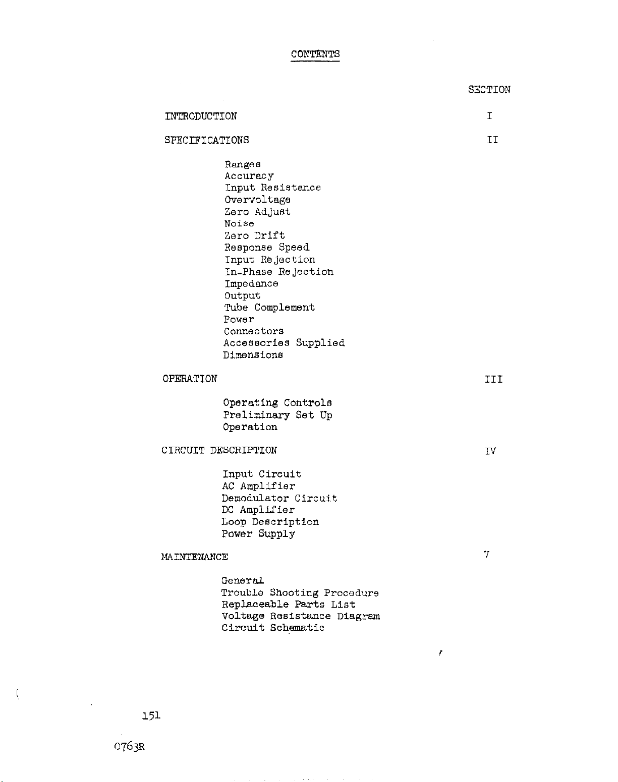
CONTENTS
SECTION
INTRODUCTION
SPJXIFICATIONS
Ranges
Accuracy
Input
Overvoltage
Zero Adjust
Noise
Zero Drift
Response
Input Rejection
In-Phase Rejection
Impedance
output
Tube Complement
power
Connector3
Accessories Supplied
Dimension3
OPERATION
Operating Control3
Preliminary Set Up
Operation
I
II
Xesl3t3ncs
Speed
III
CIRCUIT DESCRIPTION
Input Circuit
AC Amplifier
Demodulator Circuit
DC Amplifier
Loop Description
Power Supply
MAINTENANCE
General
Trouble Shooting Procedure
Replaceable Part3 List
Voltage Resistance Diagram
Circuit Schematic
151
Iv
0763
Page 3
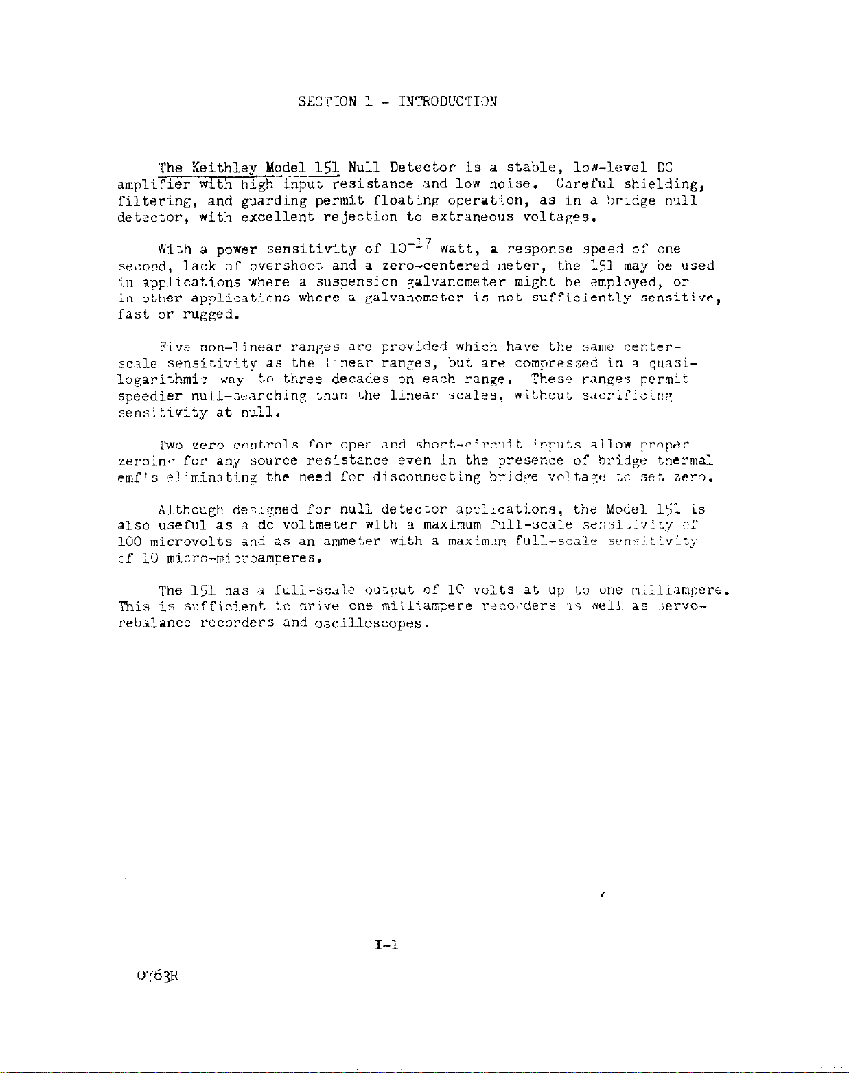
SECTION 1 - INTRODUCTION
The Keithley Model 151 Null Detector is a stable, low-level DC
amolimwith high-~<~utesistance and low noise.
fiitering,
and gu&di.nk permit floating operation, as in a bridge nuli-
Careful shielding.
detector, with excellent rejection to extraneous voltages.
With a power sensitivity of lo-l7
second, lack of overshoot and a zero-centered meter, the
watt, a re3pon3e speed of ""3
151
may be used
,;n applications Inhere a suspension galvanometer might be employed, or
in other applicaticns where a galvanometer is not sufficiently sensitive,
fast or rugged.
Five non-linear ranges are provided which have the same center-
scale sensitiv'ty as the linear ranges,
logarithmi: way to three decade3 on each range.
but are compressed in a quasi-
The3.e range3 permit
speedier null-searching th3.n the l~inear scales, without sncrlfizing
sensitivity at null.
Two zero controls for opera 2.r.d short-circuit inputs ai~low prop3r
zeroin,- for any Source resistance even in the presence of Bridge thermal
emfts eliminating the need for disconnecting bri~di=e voltage cc set zerr).
Although de?-:gned for nu?l detector applications, the Model
151
is
also useful as a dc voltmeter with 3 maximum full-scale sensi~isi~y ?f
100 microvolt3 and as an ,ammeter with a maxlm::m full-s,x1e ren:ii~tivL::.
of 10 micro-microamperes.
The 151 has i full-scale ouL.out of 10 volts at up to one mlliiamperc.
Thiv is sufficient Lo drive one milliar5~ere reco!.ders 'ii .well as ~iervorebalance recorder3 and oscilloscopes.
0763
I
I-l
Page 4
MODEL 151 ~fICROVOLTMETER
RANGE:
Linear:
ranges in lx and 3x steps.
Non Linear:
3 decades.
ACCURACY:
Linear ranges: +3% of full scale exclusive OE noise and drift.
Non-linear ranges:
ZERO DRIFT:
INPUT NOISE (with input shorted):
INPUT RESISTANCE:
LINK FREQUENCY REJECTION:
COMMON MODE REJECTION:
500,000:1.
ISOLATION:
microfarad.
chassis ground.
0.1 millivolt full scale to 10 volts on zer*-center meter.
Five ranges of 0.001, 0.01, 0.1, 1.0 and 10 volts full scal.c, eaci1 covering
?lO% of input exclusive of noise and drift
Less than 10 microvolts per day after 30-minute warm-up.
Less than 2% of fui.1 scale on ~11 r;,,r::cs
10 megohms on all ranges.
2,OOO:l
With l-megohm source resistance. dc:5,000,000:1. l.i~,le rriqut,ncv:
Circuit ground to chassis ground:
Circuit ground may be floated up to ?500 volts dc or ~p~!ak :<i!:il rcspcc: KC,
Approximately 109 ohins ijllillted 5'; ll.i!L
ILL overLappin,:
RISE TIME (10% to 90%):
OVERVOLTAGE:
ZERO ADJUST:
RECORDER OUTPUT:
Output:
Resistance:
Gain on linear ranges:
LINE STABILITY:
shift on all ranges.
CONNECTORS:
POWER:
DIMENSIONS, WEIGHT:
11-l/2 pounds.
ACCESSORIES SUPPLIED:
LOS-125 or 210-250 volts, 60 cps, 50 watts.
200 volts steady,
For both open and short-circuit inputs.
?lO volts dc at up to 1 milliampere for full-scale meter deflection.
Less than 50 ohms within the amplifier pass band.
A 10% change in line voltage will cause less than a 2,X of full-scale
Input:
Binding posts.
10 inches high x 6-l/2 inches wide x 8-l/2 inches deep; net wcighc,
Approximately L second on all ranges.
400 volts transient
10 volts
Range setting in volts
output: Amphenol 80-PC2F.
50-cps models available.
I
Mating output connector.
0166R
II-1
Page 5
SECTION III -- OPBlATION
OPERATING CONTROLS
A.
The operating controls of the Model 151 are listed below:
ON - OFF SWITCH;
RANGE SWITCH: Selects both the linear and the logarithmic ranges.
SHORT CIRCUIT ZERO:
Sets the meter zero ,with the input shorted.
This control compensates for thermal EMF's in
the connected circuit and the amplifier input.
OPEN CIRCUIT ZERO: Sets the meter zero with open or high resistance
input. This control compensates for an:, leakage
currents present in the external circuit.
B. PRELIMINARY SET UP
--
Connectto the power line. Unless otherwise marked, the unit is wired Co.117 v.,
60
cps power.
consult MAINTENANCE section.
grounds the cabinet.
To convert to 220 volt and/or 50 cps operation,
A three-wire line
cord
is furnished which
If a three-wire receptacle is not available, use
the two pin adapter furnished, and ground the third lead to an external
ground for the best operation. If open circuit unbalance is encountered,
reverse line cord.
Set the range switch to the 10 volt linear range. Xrn on the power.
In about
.1 millivolt range. Zero the meter with the SHORT CIXCUIT ZERO.
the input
30 minutes of operation some zero drift may occur and it may
30
seconds the meter will zero.
and
zero the meter with the OPEN CIRCUIT ZERO. In the first
Short the
input and
turn to the
Open
be
desirable
to reset the zeros.
USE OF ZERO CONTROLS
C.
----
The stability of the Model 151 is such that, after
30 minutes of operation,
only infrequent attention need be given to either zero co::trol except
occasionally on the most sensitive ranges.
The twc zero controls, however,
allow the user to maintain a constant zero with varying input resistances.
The short circuit zero
by thermal EMF's.
balancing any current generated by
practice, if zeroing is required, the SHOR
However,
in the case of a critical null balance application where it is
bucks
ou,t low impedance voltages such as generated
The open circuit zero is a current buckout control for
chemical
effects or leakage. In normal
T CIRCUIT ZERO is sufficient.
necessaw to eliminate zero shifi; over a range of inuut re4istances, this
can be assured by balancing the null detectcr using i,ne SHORT CIRCIJIT
ZiTiO at the lowest impedance involved and the OPEN CIHCIIIT ZERO at. the
hiphest impedance involved.
0763
III - 1
Page 6
INPUT RFSISTAlsCE AND SOURCE IMPEDANCE RIWTRICTIONS
D.
-
The input resistance of the Model 151 is 10 megohms, within 5% on the
most sensitive range and within 1% on all ether ranges. Other than the
consideration of circL.'.t loading and speed of respcnse (See F.), there
are no source impedance restrictions.
CURRENT MEASUREMENT
E.
Since the input resistance is a constant 10 megohms, ibe Model 151
bt- used '.?
full scale.
sensitive range,
measure current with a maximum sensitivity of lo-11 amperes
Since the tolerance cn input resistance is 5% on the mcst
an accuracy of about 7% can be expected there. On
may
all other ranpes an accuracy of k% is possible.
F. SPEED OF RESPONSE
--
The specification in Section II is for low impedance input. With an
open-circuit input, speed is about 5 seconds to 90% of final value.
LINE FREQUENCY REJECTION
G.
--
The specification for 60 cps rejection are given in Section II. The
rejection is high enough so that usually no precautions are necessary
with regard to 60 cps pick-up. While the input filter is specially
peaked at 60 cps for maximum rejection,
there is sufficient rejection
at other harmonics to make pickup troubles unlikely.
H. FLOATING OPERATION
The common mode rejection to DC as well as 60 cps is extremely high in
the Model151 as spwified in Section II.
with no difficulty up to 500 volts from pround.
The instrument will operate
For floating cperation,
remove the shorting link between the LO and G terminals at the front of
the instrument.
I. RECORDING
The output at the recorder terminals for ful; scale is 10 ~clts at up to
1 milliampere.
Since the output has a common ground with the input, when
recording, either the Model 151 must be grounded or the recorder input
capable of being floated.
COMected
to the output, the system rejection will be no better than that
It shoud be remembered that, with a recorder
of the recorder.
III - 2
Page 7

SECTION IV - CIRCUIT DESCRIPTION
The Model 151 is a narrow-band chopper amplifier employing negative feedback to stabilize the gain and increase the input resistance.
INPUT CIRCUIT
A.
---
The input circuit contains the dc to ac modulator, the range Switch, and
input filter to reject spurious ac Signals, and the zero controls.
The modulator used in the Model 151 employs two photoconductive cells PD 101
and PD 102 (refer to circuit schematic diagram at the rear of this manual)
which are alternately switched by two neon lamps NE 101 and NE 102 operated
from the ac line.
The action is similar to a Single-pole double-throw
mechanical chopper with the result that the dc input is converted into an
ac signal.
Spurious ac signals are prevented from entering the input by meanS of a
low-pass filter consisting o,f RlO8 and ClOL and a "twin-tee" filter consisting of RlOl +,;lrough R105 and Cl01 through Cl03 which is tuned to the
line frequency.
RlOh and R102 are set at the factory for maximum rejection
to line frequenc,v.
Below 10 millivolts, the sensitivity is changed by altering the feedback
factor. Above 10 millivolts an input divider is used.
is formed by
R153
through Rl59.
The total resistance of this divider is
The l~nput divider
10 megohms which is always across the input.
The zeroing circuits consist of batteries MO1 and MO2 and resistors
Rl38
through Rlir8.
R139 together with Rl38 and the bias batteries form
a current source which bucks out any spurious currents appearing at the
invut. Rlk8 and either R1117 or Rlb8, depending on range, place a voltage
in series with the low side of the modulator and buck-out any spurious
EMF's appearing at the ingut.
As indicated on the circuit schematic, critical parts of the input circuit
are surrounded by a Separate shield connected to the LO terminal. This
shield largely accounts for the high in-phase rejection.
AC AMPLIFIER
a.
-
The AC amplifier consists of Vl and V2.
The total gsin is approximately
500,000. The first stage tube is not Specially selected, although a tube
may have to be rejected for excessive hum pick-up which results in excessive zero offset.
Due to the excellent internal shielding of the first
stage tube, it is not necessary to use dc on the first stage filament.
The time constants of the amplifier are selected to give as narrow a
paSs-band as possible around the carrier frequency.
,
IV- 1
Page 8

DEMODUIAMR CIRCUIT
C.
The demodulator circuit employs a four-diode bridge circuit with silicon
diodes.
A balanced configuration is used so that careful balance of the
transformer secondary is not necessary.
The demodulator is driven synchronously with the neon lamps which witch
the input modulator.
The modulator output is a pulsating dc signal
which is fed through R119 to the input grid of the dc amplifier.
DC AMPLIFIER
D.
-
The dc amplifier is required for two reasons. At the carrier frequency,
the dc amplifier is a feed back integrator.
The integrating capacitor,
C115, is in a local feedback loop from output cathods to input grid.
The gain of the dc amplifier is about 500 so that the value of Cl15 is
effectively multiplied by 500,
eliminating
the need for a large value
of capacity for filtering. At dc, the demodulated signal is amplified,
increasing the loop gain by about 500.
in a ver.v high input resistance for the null-detector.
divider,
the input resistance is in excess of 300 megohms on most ranges.
This additional feedback results
Exclusive of the
The dc amplifier circuit is conventional and consists of V3 connected as
a differential amplifier, Vb used as a dc an.7lifier, and the output cathodefollow@r.
Rl28, DC AMP BAL, adjusts the balance of the dc amplifier.
Once set, this control requires very infrequent adjustment. A misadjustment is evident if, on the 10~ log range the meter is not exactly on zero.
E. THE WHOLE LOOP DESCRIPTION
---
Sections of the amplifier are combined. The input fil.ter removes any high frequency components from the input signal.
The modulator converts the filtered dc signal to ac, which is amplified
by the ac amplifier. The output of the ac amplifier is converted into a
pulsating dc signal filtered by the dc amplifier acting as an integrator,
and further amplified by the dc amplifier.
The output signal is fed back to the input by means of ~160 through R16h
and Rlh9 through Rl52.
The feedback is applied to the low end of PD102,
the modulator diode. Applying feedback at this point not only stabilizes
the gain, but raises the input resistance Vera substantially.
The sensitivity is changed from
the feedback factor.
An input divider is used above 10 millivolts.
.l millivolt to 10 millivolts by changing
The ~*logarithmicfl ranges are obtained through the use of a non-linear
"thyrite"
resistor Pi166 in the feedback loop.
?
IV - 2
0763
Page 9

On some ranges,
when the feedback factor becomes too large, it is necessary
to decrease the gain of the ac amplifier. This is done by shunting pin
7 of Q2 to ground with a small value of resistance, ~167.
F. POWER SUPPLY
Despite the high sensitivity,
no regulation is employed in the power supply,
The plus and minus supplies are derived from standard rectifier-filter
transformer ccmbinst!.cn. Points 'X nnd V on the eame transformer
are used to drive the modulator and demodulator.
winding
IV - 3
Page 10

SECTION V -- MAINTENANCE
A. GENERAL
The only periodic maintenance the Model 151 requires is replacement OC
EKDl and BAXZ, the zero set batteries, at inter-&Is of about two or three
years. If the zeroing controls become inoperative, the batteries need
replacement.
The modulator and other components have an indefinite life and should
not be tampered with unless there is a failure.
TROUBLE-SHOOTING PROCEDLIRE
B.
If the instrument is inoperative but replacement of tubes doe:: not cure
the trouble, the following step-by-step procedure is indicated.
1. Check the S-plus and B-minus voltages at the junctions of R170,
C120-B and R171,
of the voltages indirated on the schematic.
C119B.
These should agree within about
If these arelOg
markedly different, check the fuse and 'hen the ac voltage frcm
the transformer (about '23i.~ v to ground). Then check the selenium
rectifiers and the filter capacitors.
2. If the proper voltages are present in the power supply
Remove V-h, the 12AT7, from its socket, sh.crt the clltcut
a.
terminals and the input termi.nals.
5. Connec' an oscillosope to the plate of W-B (pin
Rotate the SHORT CIRCLTIT ZERO to one end of its travels.
If the ac amplifier is functioning and the bias batteries
BAl and BA2 are providing voltage, a 60 cps carrier signal,
proportional Ian amplitudeto the rotati.on of the potenticmeter (until the amplifier saturates), should be seen.
By returning the short circcit zero con'~.rcl tr midymsition,
it should be possible to reduce the signal ir i.he point
where it disappears 51; the fi~rst stage tube n, i~se.
th4.s occurs, the ac amplifier is functioning. Proceed
:n the instructions in paragraph D.
If there is an ac signal present at the output which is
C.
not affected by the short-circuit zero control, short
pin 9 of V-l to ground.
put stage shield to do this.
You will have to remove the in-
Replace it when 0bserv:r.g
the output with the oscilloscope cn pin 6 of V-2.
signal is no longer present and just background tube noise
is seen, either the modulator is defective yr the input circuit is open somewhere between Cl05 and the input terminals.
6).
If
If the
V-l
Page 11

If shorti.ng the grid does not remove the ac signal, move
the short to the grid of V-21 (pin 2). If the hum now
disappears,
either Vl is defective, Cl07 is open, or there
is excessive hum in B-plus. If the hum does not disappear,
V2 is defective or there is excessive hum in the power
supply. (At the plus terminal of
less
than 100 microvolts RMS.
ClO6,
the hum should be
At the plus termi.nal of
C12OA it should be less than 5 millivolts RMS).
If the signal still persists, remove V2 from its socket
and short pin 2 or V3 to grcund. The residual signal from
the demodulator should not exceed about 1 volt, peak to
peak. If the signal seen is still very large, replace
defective diodes RFlCs through 108. (The diodes are rated
tc pass about 1 milliampere at a five volt forward voltage
and should have about a 100 megohm back resistance).
It is also possible that the siganl observed at the plate
of V2B will be very small in amplitude and not affected
by the short-circuited zero control.
In this case either
Vl or V2 is not amplifying. To check this, place the
oscilloscope at high sensitivity at the plate of Vl (pin
and rotate the short circuit ZCI‘O control.
appears
and
is capable of being nulled, V2B ins at fault.
If the signal
6)
Once the defective amplifier stage is located, the operat-
ing points may be checked against the Voltage-Resistance
Diagram at the rear of the manual, and the defect located.
d. If no defect has been found in the ac amplifier or Ci.5
demodull.:c?,
replace V& and unshort the output.
Short
pin 2 of V3 to ground. Locate Rl28 (DC AMP BAL). On
the bench model, this control is accessible from the rear;
on the rack model, the control is located on a ceramic
board to the left rear of the instrument.
If the dc amplifier is functioning it: will'be'possible to swing the
meter pointer through zero and against both stops, al-
though the action of the control will be very coarse.
If it is not possible to swing through zero, measure the
voltage at pin 6 of V3B. When varying R128, this voltage
should swing through 100 volts.
If it will not pass
through 100 volts of the resistors associated with the
stage have changed value. Check according to the sche-
matic and the Voltage-Resistance Diagram.
I
v-2
Page 12

If the plate of V3 can be moved as indicated, move the
voltmeter to pin 2 of VhA. The voltage should pass
through zero as R128 is varied, and at least 20 volts
in the negative direction. In the positive direction,
the grid will be damped by draming grid current a few
tenths of a volt above zero. If the above is not possible, check R129, or the voltage across C119-C
(about 270~).
Now ineaaurc Vh, pin 1. This voltage should also swing
through 100 volts. If not, check as for the previous
stage.
Finally check pin 7 of VU. Since this is the cutput
cathode follower it should swing both plus and minus
at least 20 volts upon ma.*ipu1ati0* of Rl28.
If it
does not, either V&B is defective or FU3h is open.
e. In some cases, the instrument acts as if It Is extremely
sensitive, and a signal much smaller than the normal
full scale signal drives the output full scale.
The cause in this case is lack of negative feedback from
the output to the input. It may only occur on some
ranges.
It is probably due either to a defective switch
contact or a" open feedback resistor, breaking the fecd-
back loop.
It must be traced by checking with the sche-
matic and locating the resistors in question.
v-3
I
Page 13

circuit
Desig.
REPLACEADLE PARTS LIST - MODEL 151,
Description Part No.
BA-101
BA-102
c-101
c-102
c-103
c-104
c-105
C-106
c-107
C-108
c-109
c-110
c-111
Battery, Mercury aergizer,
Battery, Mercury energizer,
.047 mfd. Mylar
Sames *s c-101
.l mfd. Mylar
.l mfd. Mylar 200 v. 20% Capacitor C6G.l
Same as C-104
40 mfd. Dry Electrolytic
200 mfd. Electrolytic Upright, Capacitor
.l mfd. Paper Metalized
.02 mfd. Ceramic Disc.
2.0 mfd. Metal Tubular
.Ol mfd. Ceramic Disc.
200 v.
200 v.
1.34V (Mau0x-y
1.34V (Mallory RM-~~RT-~)BA-~~
5% Capacitor
S% capacitor c47-.l
capacitor
capacitor
Capacitor
capacitor
Capacitor
FN-lZRT-Z)BA-11
c47-.047
C27-40
C48-200
ClS-.l
c22-.02
c39-2
c22-.Ol
c-112
c-113
c-114
c-115
C-116
c-117
C-118
C-119-A
C-119-B
c-119-c Same as C-119-A
Same *B C-111
Same *s C-110
Same 88 C-108
.047 mfd. Mylar 200 v.
.OOl mfd. Ceramic Disc.
.0047 mfd. Ceramic Disc.
Same 88 C-116
30.0 mfd.
Same 88 C-119-A
Upright Can, Twist Lock Capacitor
2O?i
capacitor
capacitor
capacitor
C66-.047
c220.001
C22-,005
C52-30/30/30
I
OV%
VI-1
Page 14

Circuit
Desig.
C-120-A
REPLACEABLE PARTS LIST - MODEL 151
Description
40.0 mfd.
Electrolytic Upright Can
Part No.
capacitor C33-40/40/20
i
C-120-B
c-120-c
c-121
FU-1
ME-1
ME-1
ME-1
NE-101
I'D-101
NE-102
PD-102
PL-1
R-101
Same as C-120-A
20.0 mfd.
Same as c-109
Fuse, ; ampere - 3AG
Meter for Model 151
Meter for Model 151-R
Meter for Model 151-C
#1510, Light Modulator
#1510, Light Modulator
Pilot Light
25K.
Deposited Carbon, 4 watt, 1%
For 50 cycle Operation, RlOl is 30K
Electrolytic Upright Can
Capacitor C33-40/40/20
m-4
ha-21
ME-22
ME-32
cv-4
cv-4
PL-8
Resistor
R12-25K
R-102
R-103
R-104
R-105
R-106
R-107
R-108
R-109
R-110
10K.
48X.
20K.
54K.
333K. Deposited Carbon, k watt, 1%
18K.Ohm composition, * watt, 10%
390K. ohm Composition, 4 watt, 104.
1M.
5
Composition, Slotted Shaft
Deposited Carbon, 4 watt, 1%
Canbe&, k watt
Deposited Carbon, ij watt, 1%
for 50 cycle Operation, R105 is 65K
Deposited Carbon, + watt, 1%
Wire Wound, 5 watt, 3%
Potentiometer
Resistor
Potentiometer
Resistor
Resistor
Resistor
Resistor
Resistor
Resistor
RPlG-1OK
R12-48K
RP7-20K
R12-54K
R12-333K
Rl-18K
Rl-390K
R12-1M
R4A-5
VI-2
O-&R
Page 15

circuit
Desig.
REPLACEABLE PARTS LIST - MODEL 151
Description
Part No.
R-111
R-112
R-113
R-114
R-l.15
R-116
R-117
R-118
R-119
220 K ohm composition, gw. 10%
3.33 M ohm Deposited Carbon, $w. 1% Resistor
1 M ohm - Same as R-109
4.7 K ohm Composition, kw. 10%
1 M ohm Composition, kw. 10%
Same 8s R-115
47 K ohm Composition, fw. 1%
Same as R-115
same as R-130
R-120 Same as R-114
R-121
R-122
100 K ohm Composition, SW. 10%
Same as R-121
K-123 Same 89 R-121
Resistor
Resistor
Resistor
Resistor
Resistor
Rl-22OK
RlZ-3.33K
Ill-4.7K
$l-lbl
Rl-47K
Rl-100K
R-124
R-125
R-126
R-127
R-128
R-129
R-130
R-131
X-132
R-133
R-134
R-135
15 K ohm Composition, fw. 1%
470 K ohm Composition, kw. 10%
.5M ohm Deposited Carbon, +w. 1%
50 K ohm Deposited Carbon, +w. 1%
Resistor
Resistor
Resistor
Resistor
Rl-15K
Rl-470K
RlZ-500K
R12-50K
100 K ohm resistor is combined with ~-1.65 as & dual unit.
Same
2.2 M ohm Deposited Carbon, 4~. 1%
100 K ohm Deposited Carbon, &. 1%
*s R-109
Resistor
Resistor
R12-2.2hl
RLZ-100K
Same as R-109
Same as R-130
50 K ohm Wire Wound, 5 watt
22 K ohm Composition, 4~. 10%
Resistor '
Resistor
R4-50K
Rl-22K
0564R
VI-3
Page 16

circuit
Desig.
REPLACEABLE PARTS LIST - MODEL 151
Description
Part No.
R-136
R-137
R-138
R-139
R-142
R-143
R-144
R-145
R-146
R-147
R-146
R-149
R-150
94.5 K ohm Deposited Carbon, fw. 1%
15 K Wire Wound, 2 watt
10 K Same as R-102
1000 M ohms Composition, +w. 2%
68 K ohms Deposited Carbon, &w. 1%
Same as R-142
10 K ohms
Deposited
Carbon, fw. 1%
Same as R-144
Same 88 R-102
150 K Ohms Deposited Carbon, &I. 1%
30 K ohms Deposited Carbon, $v. 1%
10.67 ohms Deposited Carbon, $w. 1%
96 ohms Deposited Carbon, fw. 1%
Resistor
ill'&94.5K
Potentiometer RP17-15K
Resistor
Resistor
R37-10g
R12-66K
Resistor R12-10K
Resistor R12-150K
Resistor RlZ-30K
Resistor RlZ-10.67
Resistor
RlZ-96
R-151
R-152
R-153
R-154
R-155
R-156
R-157
R-158
R-159
R-160
10 ohms Deposited Carbon, 4~. 1%
100 ohms Carbon, Printed Circuit
Resistor R12-10
Potentiometer RP12-100
9.9 K ohms Deposited Carbon, l/2 W. 1% Resistor
9 M ohms Deposited Carbon, 4~. 1%
Resistor
150 K ohms Composition, fw. 10% lIea iator
667 K ohms Deposited Carbon, +I. 1%
Resistor
233 K ohms Deposited Carbon, $v, 1% Resistor
66.7 K ohms Deposited Carbon, +w. 1%
23.3 K ohms Deposited Carbon, kw. 1%
Resistor
Resistor
Same as R-109
RlZ-9.9K
R12-9M
Ill-150X
RlZ-667
R12-233K
R12-66.7X
RlZ-23.3K
I
VI-4
0564R
Page 17

circuit
Desig.
REPLACEABLE PARTS LIST - MODEL 151
Description Part No.
R-161
R-162
R-163
R-164
R-165
R-166
R-167
R-168
R-169
R-170
R-171
R-172
RF-101 Rectifier
Same BS R-106
Same PB R-131
33.3 K ohms Dspoeited Carbon, 'rw. 1%
9.9K ohms Deposited Carbon, l/2 w.
2 M ohms variable
0. E. Thyrite
33 K ohme Composition, $w. 10%
47 ohms Composition, h. 10%
Same as R-168
8.2 K ohms Composition, 2 w. 10%
1 K ohma Composition, 1 w. 10%
Same as R-121
1%
Resistor
Resistor
Resistor
Resistor
Resistor
Resistor
Resistor
Resistor
R12-33.3K
RlZ-9.9K
RPIA-2l.f -
RT-1
M-33X
Rl-47
R3-S.2K
R2-1X
RF-18
RF-102
RF-103
RF-104
RF-105
RF-106
RF-107
RF-108
RF-109
RF-110
SW-1
SW-2
T-l
Same PS RF-101
Same .LI RF-101
Same aa RF-101
Recfifisr, matched with W-l.06
Rectifier, matched
with RF-105
Rectifier, matched with ~~-108
Rectifier, mstxhed with RF-ID7
~Rectifier
Rectifier
Range Switch
Power Switch
Power Transformer
1416a.i
14163A
14168~
14168A
RF-20
RF-20
SW-7s
SW-24
TR-30
0564R
VI-5
Page 18

REPLACEABLE PARTS LIST - MODEL
15L
Circuit
Desig.
V-l
v-2
v-3
v-4
Ef=fi
- Vacuum Tube
6 Vicuum Tube
same ** v-2
l&AT7 Vacuum Tube
Dercription
Part NO.
EV &3iM &I=24
EV ?%F
EV 12-AT7
I~
f
VI-6
0564R
Page 19

F
Page 20

--
-
.-..+.
 Loading...