

Page 1
Page 2

K&~l~y~in&iwnt~, II&. ~i&&t$@i~ &oduct to b+&&om detects
Kelthley~in&&nts, Inc. ~&arrantSth~s product to befree from defects
fin metertal~ Andy workmanship~ for~e~period of 1 year from date of ship- fin metertal~ Andy workmanship~ for~e~period of 1 year from date of ship-
~~ menb During.the warranty period;~~tia~@;~at our option, either repair ~~ menb During.the warranty period;~~tia~~ill;~at our option, either repair
,~~ ,~~ ~. or ~replatie any~ product that proves~to be defective; :~ ~. or ~replatie any~ product that proves~to be defective; :~
~~ To~exercise this warranty, ~write~or $811 ~your lo&Kehhley~mpreesnt-:
~~~ ~~ ~~~ ~~
~~ ~~ ~~ ~~
.~ ~~ ~~~ .~ ~~ ~~~
~~ To~exercise this warranty, ~write~or $811 ~your
ative, ,or contacts Keithley headquarters in Cleveland, ohlti.~You~will~be ative, ,or contacts Keithley headquarters in Cleveland, ohlti.~You~will~be
given prompt assistance and return instructions, Send:the instrument; given prompt assistance and return instructions, Send:the instrument;
~‘~ transportation prepaid; to the indir+sd service f&lii~ jIegairs @l be ~‘~ transportation prepaid; to the indir+sd service f&lii~ jIegairs @l be
~rnade~ land the~~instrument returned,~ transpotitiort prepeid.~ R~epaired ~rnade~ land the~~instrument returned,~ transpotitiort prepeid.~ R~epaired
products~are~vyarrsnted fork the:bMance of the origin8~warianty period, products~are~vyarrsnted fork the:bMance of the origin8~warianty period,
~~ ~~ or at least 90 ~days. or at least 90 ~days.
:
LIMITATION~~OF~WARAANTV~~
:
LIMITATION~~OF~WARAANTV~~
This warranty does not epply~to ~defectsresulting~ from unauthorized This warranty does not epply~to ~defectsresulting~ from unauthorized
mpdification or misuse oft any product or part. This warmnty al&o does mpdification or misuse oft any product or part. This warmnty al&o does
~~ not spply to~fuses; batter@, or damage from ~battery leakege~~ ~~ ~~ not spply to~fuses; batter@, or damage from ~battery leakege~~ ~~
This werranty is in lieu,of all other &rranties, expra$ed or implied, in- This werranty is in lieu,of all other &rranties, expra$ed or implied, in-
dluding~ any implied ~warranty of :merchentability nor f%ne& -for a par; dluding~ any implied ~warranty of :merchentability nor f%ne& -for a par;
ticularuse; Keithley Instruments, ~lnti. shall not bs IiabMfor any indirect, ticularuse; Keithley Instruments, ~lnti. shall not bs IiabMfor any indirect,
special nor coosequential~damsges. ~~~ ~~~~ special nor coosequential~damsges. ~~~ ~~~~
;’ ~~~
;S~~~EM~E,N~T~OF~CAL1BRATION
;S~~~EM~E,N~T~OF~CAL1BRATION
l6&Keithiey~~p~epresent-:
~~ ~~
Ran ~: : ~~ ;’ ~~~
Ran ~: : ~~
~~~ This ~itiStrument~ has, been~ inspected land t&tedin~ crCcOrdance v&h ~~~ This ~itiStrument~ has, been~ inspected land t&tedin~ crCcOrdance v&h
specifications bublishedby Keithley instruments, fin& ~~ specifications bublishedby Keithley Instruments, fin& ~~
: The~at%uracy and calibration~of this instrument am traceable to the ~~ : The~at%uracy and calibration~of this instrument am traceable to the ~~
~Nationat ~Bureau of Standards through equipment which is cal~@reted at ~Nationat ~Bureau of Standards through equipment which is cal~@reted at
,~ fWrned ~Jnterv& by comparisqn to ,~ertlfii Standards maintained in
,~ @anned ~Jntery&ls~ by comparisqti !a ,~et$fii standafds nMin@nad in
the Laboratories of :Keithley lnstruments;~ Inc. the Laboratories of :Keithley Instruments;~ Inc.
Page 3

INSTRUCTION MANUAL
Model 148
Nanovoltmeter
COPYRIGHT 1974, Keithley Instruments, Inc.
PRINTED JAN. 1979, CLEVELAND, OHIO U. S. A.
DOCUMENT #29029
Page 4
CONTENTS
Page 5
MOOEI, 148
ILlsJSTRATIONS
ILLUSTRATIONS
FIG. TITLE PACE
la Front Panel ................................
lb Front Panel With Model 1481 Input Cable
2
Front Panel Conrrole. ...........................
3 Rear Panel Conerols and Connections
4
Model 1481 Low-Thermal Input Cable.
5 Made! 1483 Low-Thermal Connection Kit
6 Normal Wave Form at Demodulator with Input Sbor’ted.
7 Wave Format Demodulator Sham with Some Pickup.
8
Wave Format Demodulator when Amplifier is Saturated
9 “sing Model 148 with 4-Terminal Connections
10 Exploded “few far Rack Mounting
11 Block Diagram of Model 148 Amplifier Circuits
12
13 Block Diagram of Model 148 Power Supplies
14 Model 148 Input Compartment
15 Correct Wave Form in dc-to-dc Inverter.
16 correct wave Form at Point F in Oscillator circuit.
17 Improper wave Form af point F in Oscillator Circuit
18 NOf Used.
19 Nof Used. .................................
20 Top View of Model 148 massis
21 Bottom View of Model 148 Chassis.
22 Transistor Locations on Printed Circuit 76.
23 Capacitor and Diode Locations on Printed Circuit 76
24
25 Resistor and Test Point Locations on Printed Circuit 76
26
27 Component Locations on Printed Circ”it 74, Top Face
28 Resistor and Test Point Locationa on Printed Circuit 75
29 Capacitor and Transistor Locations on Printed Circuit 75.
30
31 Resistor LOcationS on RANOE SWitCh (5102)
Model 148 Input Circuit
.................................
Resistor Locations on Printed Circuit 76.
Resistor and Test Point Locations on Printed Circuit 74. Bottom Face.
Resistor Locations on RANGE Switch (S102)
.......................... 20
...................... 18
........................ 26
....................... 38
.................. 3
.................... 6
.................... 10
............ : ...... 10
............ 15
.............. 15
............ IS
................ 17
............... 19
................. 23
.................. 31
............ 32
............ 32
..................... 39
................ 40
............ 40
................. 41
............ 42
................. 44
................. 44
--
--
.......... 41
.......... 4,
.........
... 42
43
1
4
0375
Page 6

SPECIFICATIONS
MODEL 148
SPECIFICATIONS
iv
0375
Page 7

MODEL 148
GENERAL DESCRIPTION
SECTION 1.
GENERAL DESCRIPTION
l-l. GENERAL.
The Keithley Model 148 Nanovoltmeter conveniently measures dc potentials
a.
from 10 nanovolts (10 x 10-g
volts) to 100 millivolts full scale. It makes
accurate and sensitive measurements without painstaking methods often previously
required.
Meter accuracy is 2% of full scale on all ranges.
than 1 nanovolt peak-to-peak on the lo-nanovolt range.
than 10 nanovolts per 24 hours after warm-up.
On the three most sensitive
Zero drift is less
Noise is less
ranges, line-frequency rejection is greater than 1OOO:l.
For reliable and versatile use,
b.
design, except for the first two input stages.
the Nanovoltmeter is of solid-state
It has high line isolation
and battery or line operation.
0972
FIGURE la. Front panel.
Page 8

GENERAL DESCRIPTION
MODEL 148
1-2.
ing many grounding problems.
FEATURES.
Battery operation permits complete isolation from power line, eliminat-
a.
Battery operation also allows flexibility and
convenience in use. The Model 148 automatically recharges the battery if
needed when the ac power cord is connected.
The Nanovoltmeter has a 21 volt at 1 milliampere output at full-scale
b.
meter deflections for driving a recorder or oscilloscope.
Accuracy is 1% of
full scale for output.
c. A zero suppression circuit permits measuring small changes in a larger
dc signal.
l-3. APPLICATIONS.
The Model 148 Nanovoltmeter measures very small dc potentials or
a.
small changes in dc potentials from low impedance sources. These are found
in fundamental or applied research, laboratory standards work, cryogenic
experiments and instrument development for space research.
It can also
serve as an amplifier in these uses.
Typics.1 uses include measuring small temperature differences and
b.
small temperature changes indicated by thermocouple outputs, small changes
in conductance,
outputs used in narrowband spectrum analysis.
the thermoelectric power of metals,
making Bolometer
super conductivity in the lo-6 ohm range, and thermopile
Other uses are determining
conducting Hall effect studies, and
measurements.
Also, the Model 148 is suited for use with
potentiometers, ratio sets and resistance bridges, including Wenner, Wheatst
and Kelvin Double bridges. It can be used to make 4-terminal resistance
measurements.
2
0972
Page 9

MODEL 148 GENERAL DESCRIPTION
0972
FIGURE lb.
Front Panel With Model 1481 Input Cable.
3
Page 10
GENERAL DESCRIPTION
ZERO s”PPmssIoN
POWER
SWITCH
5201 COARSE 5103
MODEL 148
*
FINE R168
4
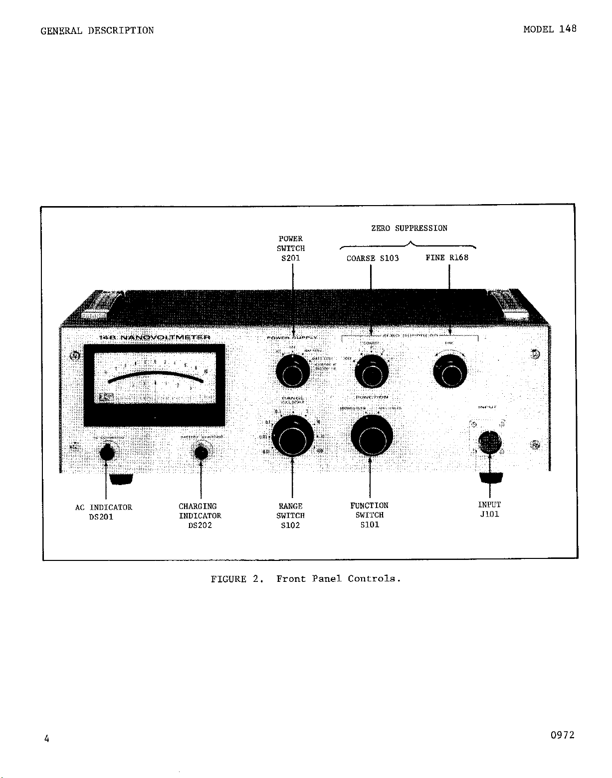
FIGURE 2. Front Panel Controls.
0972
Page 11

MODEL 148 NANOVOLTMETER
OPERATION
SECTION 2.
.2-l. FRONT PANEL CONTROLS.
a. AC CONNECTED Lamp.
The Lamp is lit whenever the unit is connected to
(See Figure 2.)
OPERATION
the ac line and the POWER SUPPLY Switch is in the AC or OFF position.
NOTE
The AC CONNECTED Lamp indicates only that the instrument
is connected to the ac power line; it does not indicate
that the Nanovoltmeter is operating.
Also, when the
POWER SUPPLY Switch is turned from AC to OFF, a difference
in Lamp brightness is normal.
BATTERY CHARGING Lamp. When lit,
b.
charging.
not lit,
POWER SUPPLY Switch.
c.
The charge current determines its brightness.
then the battery is charged.
The Switch controls the mode of operation for
this Lamp indicates the battery is
If the lamp is
the power supply.
AC position:
1.
The battery will be charged if needed; then,
The Nanovoltmeter will operate from the ac power lint.
the BATTERY CHARGING Lamp
will light.
OFF position: The Model 148 is not operating.
2.
will be charged,
BATTERY position:
3.
if needed and if the power cord is connected.
The Nanovoltmeter is operated from its battery.
The ac power line is internally disconnected;
However )
the AC CONNECTED Lamp is off;
tk! battery
the battery cannot be charged.
BATT.TEST position:
4.
When the POWER SUPPLY Switch is held in this
position, the Model 148 shows the state of the battery charge directly
on its meter. All circuits within the instrument are the same as for
battery operation except at the meter terminals.
Switch Settin
TABLE 1.
Indicating Lamps and POWER SUPPLY Switch Settings.
The table shows the relationship between the front panel
lamps,
the power cord and the POWER SUPPLY Switch setting.
Page 12

OPERATION
MODEL 148 NANOVOLTKETER
RANGE Switch.
d.
The RANGE Switch selects the full-scale meter sensitivity
(either microvolts or millivolts) for one of nine ranges, from 0.01 to 100.
FUNCTION Switch.
e.
The FUNCTION Switch selects the function - MICROVOLTS
or MILLIVOLTS - which is to be measured.
ZERO SUPPRESS Controls.
f.
The COARSE Control disconnects the suppression circuit (in OFF position)
1.
or selects one of four suppression voltages in decade steps.
The FINE Control is a continuously variable adjustment for the suppression
2.
voltage set by the COARSE Control.
Two controls determine the amount of zero suppression.
Refer to Table 3.
It adjusts the range between the positive
and negative values of the maximum voltage set by the COARSE Control.
INPUT Receptacle.
g.
The INPUT Receptacle is of a special low-thermal design.
Use only the Models 1481, 1482 and 1486 for mating connectors.
5103:
FIGURE 3. Model 148 Rear Panel Controls and Connections.
refer to Replaceable Parts List and schematic diagrams.
2-2.
REAR PANEL CONTROLS AND CONNECTIONS.
Line Voltage Switch. The screwdriver-operated slide switch sets the
a.
Model 148 for 117 or 234~volt ac power lines.
Fuse.
b.
For 117~volt operation,
1.
For 234volt operation, use only a MDL Slow-Blow l/16-ampere fuse.
2.
Power Cord. The 3-wire power cord with the NEMA approved 3-prong plug
c.
provides a ground connection for the cabinet.
use a 3 AG or MDL Slow-Blow l/8-ampere fuse.
An adapter for operation from
2-terminal outlets is provided.
WER
RD
Circuit designations
6
0464
Page 13
MODEL 148 NANOVOLTMETER
A note above the power cord shows the ac power line frequency
for which the rejection filter is adjusted.
will work at any line frequency from 50 to 1000 cps, but ac
rejection is best at the indicated frequency.
OPERATION
The instrument
DEMODULATOR TEST.
d.
A phone jack provides access to the demodulator for
test purposes.
e.
OUTPUT.
The OUTPUT Receptacle provides fl volt at one milliampere for
a full-scale meter deflection on any range.
GND and LO Terminals. The ground terminal (GND) is connected to the chassis
f.
and the third wire of the power cord. The low terminal is connected to
circuit ground and the low side of the input connection.
2-3.
or from its battery. For most uses,
operation, however,
problems.
MODE OF OPERATION. The Model 148 operates either from an ac power line
it functions well from ac. Use battery
if the ac power line will create ground loop or isolation
Isolation from low to ground is complete for battery operation
when the power cord is disconnected; it is greater than 10' ohms with the power
cord connected. Also use battery operation to reduce the 8-cps ripple which
may appear at the output with the input shorted in ac operation.
See
paragraph Z-13.
NOTE
Before using the battery operation, thoroughly read paragraph 2-4.
Inproper
to
inaccurate
battery
measurements.
operation can damage the
battery
pack and lead
2-4. BATTERY OPERATION.
The Model 148 is supplied w;th a rechargeable 6-volt, 4 ampere-hour
a.
nickel-cadmium battery pack. Re<,c~mmended:
than eight consecutive hours without recharging.
rate /
the battery should last about 1000 recharge cycles.
Do not use the battery more
At this discharge
NOTE
Permanent damage to the battery pack occurs if it is used
for more than 14 consecutive hours without recharging.
At this discharge rate, the recharge cycles are greatly
reduced.
Before using the Model 148, check the state
of the battery charge.
Check the battery charge before making a measurement. Hold the
b.
POWER SUPPLY Switch in the BATT. TEST position.
The minimum acceptable
charge is a meter indication of +8; full charge is shown by the BATTERY
CHARGING Lamp not being lit.
Recharge if needed. Otherwise,
battery operation is the same as for the ac power line operating mode;
refer to paragraph 2-5.
1067'
7
Page 14
OPERATION
MODEL 148 NANOVOLTMETER
NOTE
When the battery is used beyond its capacity, two effects
are seen.
There is a shift in zero offset from ac to
battery operation. Also, the power supplies do not regulate and high ripple voltages appear at the supply outputs.
(See paragraph 4-7.)
To recharge the battery,
c.
come-t the power cord to an ac power line.
the POWER SUPPLY Switch to AC or OFF.
The BATTERY CHARGING lamp will light. The
Turn
battery will be charged only if needed, and the circuit automatically prevents
it from being overcharged.
It is suggested that the battery be used during the day and be recharged
d.
at night.
Leave the instrument always connected to the ac power line; then
turn the POWER SUPPLY Switch to OFF at night, After a fully charged battery
is used for eight consecutive hours, it will recharge within 14 hours.
the power cord connected has little effect on the isolation:
109 ohms with
Leaving
the POWER SUPPLY Switch in BATTERY position and the low-ground link disconnected.
2-5. OPERATING PROCEDURES,
Set the front panel controls as follows:
a.
POWER SUPPLY Switch OFF
FUNCTION Switch MILLIVOLTS
RANGE Switch 100
ZERO SUPPRESS COARSE Control OFF
NOTE
Make sure the ZERO SUPPRESS COARSE Control is OFF. If it is not,
a suppression voltage is introduced, causing an error in measurements.
Connect the unknown voltage source to the INPUT Receptacle.
b.
Refer to
paragraph 2-6 for suggestions.
Check the voltage shown on the rear panel Line Voltage Switch; connect the
c.
Model 148 to the ac power line. Make sure the frequency shown above the power
cord is the frequency of the ac power line. At this point, the AC CONNECTED Lamp
will light, as will the BATTERY CHARGING Lamp if the battery is being charged. If
the circuit low is to be at ground, put the low-ground link between the LO and
GND terminals on the rear panel.
Turn the POWER SUPPLY Switch to the desired mode of operation, AC or BATTERY.
d.
Increase the sensitivity of the Model 148 until the
e.
meter
shows the greatest
on-scale deflection.
Check the source resistance to make sure it is within the maximum value
1.
specified for the range being used. (See Table 2.) If the maximum resistance
is exceeded, the Model 148 may not be within its specifications.
1067
Page 15
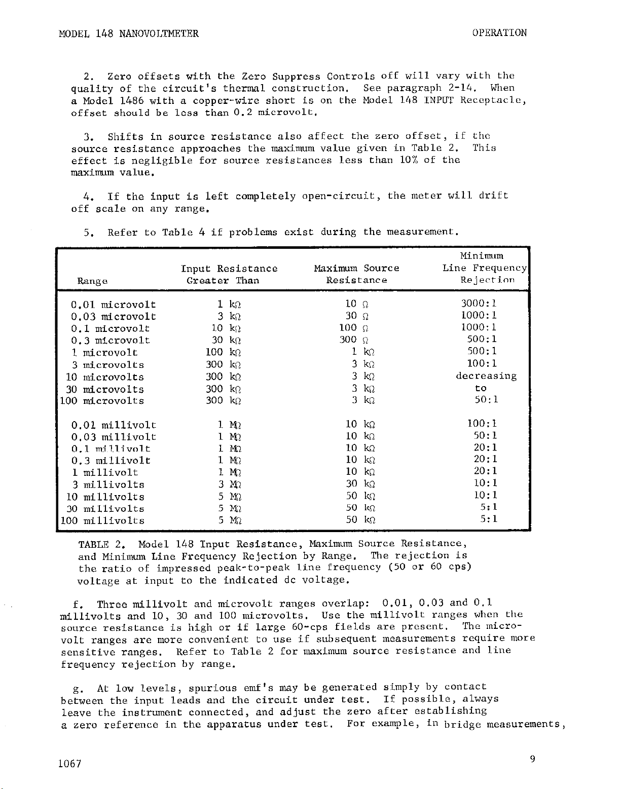
MODEL 148 NANOVOLTMETER OPERATION
Zero offsets with the Zero Suppress Controls off will vary with the
2.
quality of the circuit's thermal construction. See paragraph 2-14.
a Model 1486 with a copper-wire short is on the Model 148 INPUT Receptacle,
offset should be less than 0.2 microvolt.
Shifts in source resistance also affect the zero offset, if the
3.
source resistance approaches the maximum value given in Table 2.
effect is negligible for source resistances less than 10% of the
maxiwm value.
If the input is left completely open-circuit, the meter will drift
4.
off scale on any range.
Refer to Table 4 if problems exist during the measurement.
5.
Minimum
Input Resistance Maximum Source Line Frequent
Range Greater Than Resistance Rejection
when
This
0.01 microvolt
0.03 microvolt
0.1 microvolt
0.3 microvolt
1 microvolt
3 microvolts
.O microvolts 300 kll
i0 microvolts 300 kn
10 microvolts 300 krl
0.01 millivolt
0.03 millivolt
0.1 millivolt
0.3 millivolt
1 millivolt
3 millivolts
.O millivolts
IO millivolts
10 millivolts
TABLE 2. Model 148 Input Resistance, Maximum Source Resistance,
and Minimum Line Frequency Rejection by Range.
the ratio of impressed peak-to-peak line frequency (50 or 60 cps)
voltage at input to the indicated dc voltage.
1 kcl
3 kcl 30 n
10 kn
30 kn
100 lcrl
300 kn 3 kc1
1 I%,2
1lQ
l?Sl 10 kn
1 Ma.
1Kl
3Kl
5 Ml
5 I%1
5 Nl
10 n
100 n
300 11
1 lu?
3 kn
3&l
3kn
10 kn
10 kcl
10 kn
10 kn
30 m
50 Icn
50 k!J 5:l
50 kn
The rejection is
3OOO:l
1OOO:l
1OOO:l
5OO:l
5OO:l
1OO:l
decreasing
to
5O:l
100: 1
5O:l
2O:l
2O:l
2O:l
1O:l
1O:l
5:l
Three millivolt and microvolt ranges overlap: 0.01, 0.03 and 0.1
f.
millivolts and 10, 30 and 100 microvolts.
source resistance is high or if large 60-cps fields are present.
volt ranges are more convenient to use if subsequent measurements require more
sensitive ranges.
frequency rejection by range.
At low levels,
g.
between the input leads and the circuit under test.
leave the instrument connected, and adjust the zero after establishing
a zero reference in the apparatus under test.
1067
Refer to Table 2 for maximum source resistance and line
spurious emf's may be generated simply by contact
use the millivolt ranges when the
The micro-
If possible, always
For example,
in bridge measurements,
9
Page 16
MODEL 148 NANOVOLTMETER
disconnect the bridge exciting voltage; or with a phototube, shield the tube
from light.
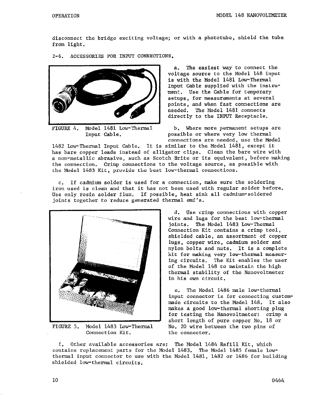
2-6. ACCESSORIES FOR INPUT CONNECTIONS.
a. The easiest way to connect the
voltage source to the Model 148 input
is with the Model 1481 Low-Thermal
Input Cable supplied with the instru-
ment.
Use the Cable for temporary
setups, for measurements at several
points, and when fast connections are
needed. The Model 1481 connects
directly to the INPUT Receptacle.
I
FIGURF: 4.
Model 1481 Low-Thermal
Input Cable.
possible or where very low thermal
Where more permanent setups are
b.
connections are needed, use the Model
1482 Low-Thermal Input Cable. It is similar to the Model 1481, except it
has bare copper leads instead of alligator clips.
Clean the bare wire with
a non-metallic abrasive, such as Scotch Brite or its equivalent, before making
the connection. Crimp connections to the voltage source, as possible with
the Model 1483 Kit, provide the best low-thermal connections.
If cadmium solder is used for a connection, make sure the soldering
C.
iron used is clean and that it has not been used with regular solder before.
Use only rosin solder flux.
If possible, heat sink all cadmium-soldered
joints together to reduce generated thermal emf's.
Use crimp connections with copper
d.
wire and lugs for the best low-thermal
joints.
The Model 1483 Low-Thermal
Connection Kit contains a crimp tool,
shielded cable, an assortment of copper
lugs,
copper wire, cadmium solder and
nylon bolts and nuts. It is a complete
kit for making very low-thermal measur-
ing circuits. The Kit enables the user
of the Model 148 to maintain the high
thermal stability of the Nanovoltmeter
in his own circuit.
The Model 1486 male low-thermal
e.
input connector is for connecting custommade circuits to the Model 148. It also
makes a good low-thermal shorting plug
for testing the Nanovoltmeter: crimp a
short length of pure copper No. 18 or
'IGURE 5. Model 1483 Low-Thermal
Connection Kit.
No. 20 wire between the two pins of
the connector.
Other available accessories are:
f.
contains replacement parts for the Model 1483.
The Model 1484 Refill Kit, which
The Model 1485 female low-
thermal input connector to use with the Model 1481, 1482 or 1486 for building
shielded low-thermal circuits.
10
0464.
Page 17
MODEL 148 NANOVOLTMETER
2-7. ZERO SUPPRESS OPERATION.
OPERATION
Purpose:
a.
order to use a more sensitive range to observe a superimposed signal.
100 times full scale may be suppressed on the ranges from 0.1 millivolt to
0.01 microvolt. For example, the Model 148 can measure changes of less than
one microvolt in a lOO-microvolt steady signal on its l-microvolt range.
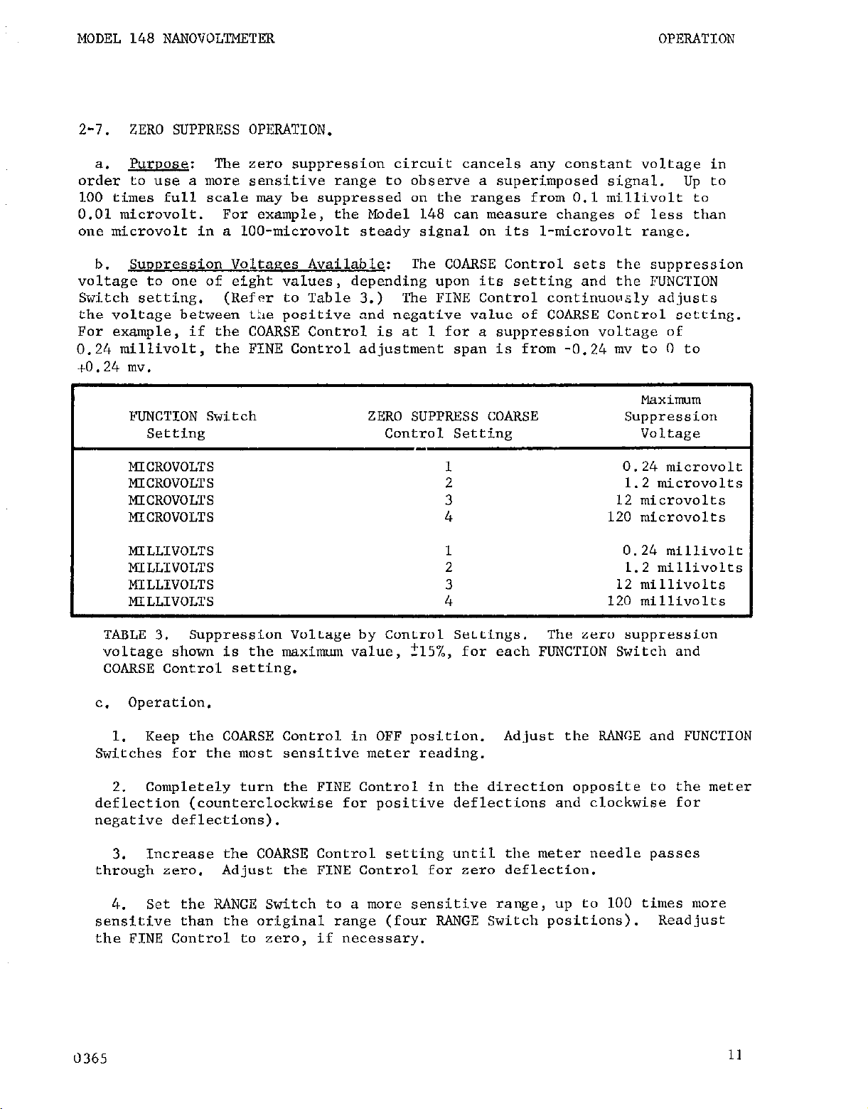
Suupression Voltaxes Available: The COARSE Control sets the suppression
b.
voltage to one of eight values, depending upon its setting and the FUNCTION
Switch setting. (Refer to Table 3.) The FINE Control continuously adjusts
the voltage between tile positive and negative value of COARSE Control setting.
For example, if the COARSE Control is at 1 for a suppression voltage of
0.24 millivolt,
+0.24 mv.
FUNCTION Switch
Setting
MICROVOLTS
MICROVOLTS
MICROVOLTS
MICROVOLTS
MILLIVOLTS 1 0.24 millivolt
MILLIVOLTS 2 1.2 millivolts
MILLIVOLTS 3 12 millivolts
MILLIVOLTS 4 120 millivolts
The zero suppression circuit cancels any constant voltage in
up to
the FINE Control adjustment span is from -0.24 mv to 0 to
Maximum
ZERO SUPPRESS COARSE
Control Setting
1
2
3
4
Suppression
Voltage
0.24 microvolt
1.2 microvolt6
12 microvolt6
120 microvolt6
TABLE 3.
voltage shown is the maximum value, ?15%, for each FUNCTION Switch and
COARSE Control setting.
c. Operation,
Keep the COARSE Control in OFF position.
1.
Switches for the most sensitive meter reading.
Completely turn the FINE Control in the direction opposite to the meter
2.
deflection (counterclockwise for positive deflections and clockwise for
negative deflections).
Increase the COARSE Control setting until the meter needle passes
3.
through zero.
Set the RANGE Switch to a more sensitive range, up to 100 times more
4.
sensitive than the original range (four RANGE Switch positions).
the FINE Control to zero, if necessary.
Suppression Voltage by Control Settings. The zero suppression
Adjust the RANGE and FUNCTION
Adjust the FINE Control for zero deflection.
Readjust
0365
11
Page 18
OPERATION
MODEL 148 NANOVOLTMETER
NOTE
On the highest zero suppression range - 120 millivolts maximum - a zero offset
will be apparent when changing the RANGE Switch settings. On this zero suppres-
sion range, first set the RANGE Switch to the range intended to be used. Then
zero the meter with the ZERO SUPPRESS FINE Control. This offset is introduced
only when the ZERO SUPPRESS COARSE Control is set to 4 and the FUNCTION Switch
is set to MILLIVOLTS. There is no significant offset on any other zero supprss-
sion range.
2-8. DIFFERENTIAL MEASUREMENTS.
The Model 148 will measure the difference between two voltages, neither or which is
a.
at power line ground. It can be floated up to 1-400 volts off ground in ac operatior
the Model 148 is battery operated it is completely isolated from line.
Unplug the Model 148 power co? and use battery operation before measuring a
source which is more than f400 volts instantaneous off ground.
Damage to the
instrument can result if the power line is connected under these conditions.
When
CAUTION
The front panel controls are electrically connected to the case.
"cord is unplugged,
Use necessary safety precautions.
For best results in making differential measurements, follow the steps below:
b.
Remove the link from the LO or GND terminal on the rear panel.
1.
Connect the voltage source to the Nanovoltmeter i,L,wt.
2.
scribed in paragraph 2-5.
urements.
Do not ground any recorders used with this operation, since the low of the
the case may be at a voltage equal to the off-ground voltage.
Make measurements as de-
The zero suppress controls may be used for differential meas-
If the power
Model 148 output is no longer grounded.
3. If power line frequency pickup is a problem, battery operation usually provides
better results.
2-9. RECORDER OUTPUT.
on any range is *l volt at one milliampere.
tance is less than 5 ohms within the amplifier pass band.
ac and battery operation.
The output of the Nanovoltmeter for a full-scale meter deflection
Accuracy is 1% of full scale. Output resis-
Output may be used during both
If the Model 148 is used for differential meas?xements, do not
ground the recorder connected to the output.
When recording the Keithley Model 370 Recorder offers complete compatibility with
a.
the Model 148. The output is sufficient to drive the Model 370 without the use of any re-
corder preamplifiers. The Model 370 allows maximum capability of the Model 148.
1% linearity, 10 chart speeds and can float up to *500 volts off ground.
Using the Model
It has
370 with the Model 148 avoids interface problems which may be encountered between a meas-
uring instrument and a recorder.
The Model 370 is very easy to use with the Model 148. All that is necessary is con-
b.
necting the two units and adjusting an easily accessible control for full-scale recorder
12
1067
Page 19

MODEL 148 NANOVOLTMETER
OPERATION
L
Trouble (seen on meter)
Change in offset between ac
Possible Cause
Low Battery
Refer to
paragraph 2-4
and battery operation
Very slow response time
High source resistance paragraph 2-12
Improper shielding paragraph 2-13
Excessive drift
I I
Thermal emfs
paragraph 2-14
I
Improper connection to input paragraph 2-15
Excessive noise or needle
instability
High source resistance paragraphs 2-11,2-l
improper shielding paragraph 2-13
Improper connection to input
paragraph 2-15
Thermal emfs paragraph 2-14
Excessive temperature sensitivity Thermal emfs
paragraph 2-14
presence of large, constant zero suppress Controls on paragraph 2-5
signal Thermal emfs paragraph 2-14
Improper connection to input paragraph 2-15
Excessive 8-cps beat at output
or meter magnetic shielding
I
TABLE 4.
Troubleshooting Operating Procedures. *he Table gives some possible sources of
Improper location or poor
I
paragraph 2-13
I
errors while using the Model 148 and refers to instructions to correct the situation.
deflection. The furnished Model 3701 Input Cable mates with the output connector on the
Model 148. On the most sensitive ranges of the Model 148, under some conditions, a" 8-
cps beat may appear. This condition can be eliminated by mounting a 100~microfarad capac-
itor across pins 14 and 17 in the back of the Model 370 Recorder.
2-10.
ACCURACY CONSIDERATIONS.
For sensitive measurements - 10 millivolts and below -
other considerations beside the voltmeter affect accuracy. The Model 148 reads only the
signal received at its input; therefore, it is important that this signal be properly
transmitted from trle source. The following paragraphs indicate factors which affect ac-
CllrWy: thermal noise, loading, shielding, thermal emfs and circuit connections.
Table
4 also offers a quick reference to correct troubles which may occur.
2-11 THERMAL NOISE.
The lower limit in measuring small potentials occurs when the Johnson noise, or
a.
thermal agitation, becomes evident. The amount of noise present in the source is show" in
the following equations.
1. The thermal noise in any ideal resistance can be determined from the Johnson noise,
equation:
-As
=4kTRF Eq. 1
where Er,, is the rms noise voltage developed across the voltage source;
T is the temperature in degrees Kelvin;
1067
13
Page 20
OPERATION MODEL 148 NANOVOI~'~ETEl?
R is the source resistance in ohms;
F is the amplifier bandwidth in cps;
k is the Boltzmann constant (1.38 x lo-23 joules/OK).
For an ideal resistance at room temperature (300°K), equation 1 simplifies to
rms = 1.29 x lo-lo (R F)112
Peak-to-peak meter indications are of more interest than the rms value.
2.
mentally,
E
the peak-to-peak Johnson noise is about five times the rms value.
Eq. 2
Experi-
At room
temperature, equation 2 becomes
= 6.45 x lo-10 (R F)li2
EPP
Eq. 3
where Epp is the peak-to-peak noise voltage developed across the voltage source.
The Model 148 bandwidth, F,
3.
can be estimated from the response speed, tr, by:
F = 0.35/tr Eq. 4
The response speed varies with the range used and the source resistance.
On the O.l-
microvolt range when the source resistance is less than 10 ohms, for example, the bandwidth is greater that 0.7-cps.
The maximum specified response speed for this situation
is 0.5 second, so the 0.7-cps bandwidth is a minimum value.
As an example, determine the Johnson noise of a lo-ohm ideal resistor. Measured
4-
with the Model 148 on the 0.1~microvolt range and using equation 3, this becomes
17.1 x lo-10 volts peak-to-peak or 1.71 nanovolts peak-to-peak minimum.
In general, good wirewound or low-noise metal-film resistors approximate ideal resis-
b.
tors,
and equations 2 and 3 are nearly correct. If the source resistance is.composed of
other materials, it may be necessary to include other terms in the equations to account
for flicker, l/f, and current noise over and above the thermal noise.
c. As seen in equations 2 and 3,
ficant in the microvolt region.
fore, keep the source resistance as low as possible.
the noise of even low resistance values becomes signi-
The noise in non-ideal resistors is even greater. There-
Other effects of high source resis-
tances are decreased response speed and added pickup of extraneous voltages.
2-12. INPUT RESISTANCE.
is obtained by using high feedback factors.
The Model 148 is a feedback amplifier, and its input resistance
When the source resistance exceeds its physi-
cal input resistance - the amplifier without feedback - the feedback is partially de-
stroyed.
higher resistances may be used, but noise, offset,
result.
Normally, do not exceed the maximum source resistance specified in Table 2;
slow response time and instability may
On the most sensitive ranges,
the maximum source resistance is consistent with
Johnson noise considerations.
Z-13. SHIELDING.
Due to its narrow bandwidth, the Model 148 is somewhat insensitive to ac voltages
a.
superimposed upon a dc signal at the input terminals.
However,
ac voltages which are
large compared with the dc signal may drive the Model 148 ac amplifier into saturation,
erroneously producing a dc output
at
the demodulator.
Therefore, shield the circuit to
the Nanovoltmeter input, particularly for low-level sources.
14
1067
Page 21
MODEL 148 NANOVOLTMETER OPERATION
Improper shielding can cause the Model 148 to react in one or more of
b.
the following ways:
Needle jitter or instability, from 10% to 20% of full scale.
1.
High offset (dc bias). Changing the power cord polarity or the
2.
connection between the LO and GND terminals may affect the amount of offset.
Slow response time, sluggish action and/or inconsistent readings
3.
between ranges.
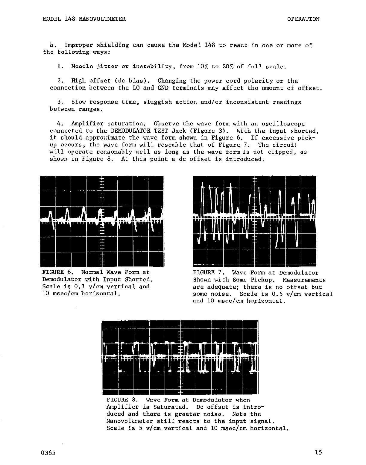
Amplifier saturation.
4.
Observe the wave form with an oscilloscope
connected to the DEMODULATOR TEST Jack (Figure 3). With the input shorted,
it should approximate the wave form shown in Figure 6. If excessive pickup occurs, the wave form will resemble that of Figure 7. The circuit
will operate reasonably well as long as the wave formis not clipped, as
shown in Figure 8.
---
FIGURE 6.
Normal Wave Form at
Demodulator with Input Shorted.
Scale is 0.1 v/cm vertical and
10 msec/cm horizontal.
At this point a dc offset is introduced.
FIGURE 7.
Wave Form at Demodulator
Shown with Some Pickup.
are adequate;
some noise.
there is no offset but
Scale is 0.5 v/cm vertical
Measurements
and 10 msec/cm ho,rizontal.
0365
FIGURE 8. Wave Form at Demodulator when
Amplifier is Saturated. DC offset is intro-
duced and there is greater noise. Note the
Nanovoltmeter still reacts to the input signal,
Scale is 5 v/cm vertical and 10 msecfcm horizontal.
15
Page 22

OPERATION
To minimize pickup, keep the voltage source and the Nanovoltmeter away
c.
from ac sources.
at the low side of the input or at the LO terminal.
magnetic flux is proportional to the area of the loop.
areas in the shield connections as well as the input circuitry.
at only one point. Run all wires in the circuit along the same path, so the
loop area is only the small difference in position of two adjacent wires.
Shield as carefully as possible.
MODEL 148 NANOVOLTMETER
Connect all shields together
The voltage induced due to a
Therefore, minimize loop
Connect the shield
Strong third harmonic magnetic fields
d.
create an 8-cps beat at the Nanovoltmeter output and meter.
effect, turn off all possible nearby sources,
Remove the Model 148 and the measuring circuit as far as possible from the
magnetic field.
as electrostatic shielding around the circuit may be necessary.
tion concerning your particular shielding problem,
1322 North Elston Street, Chicago, Illinois.
Shielding is preferable to input filters.
e.
add noise (see Johnson noise equation),
tracted from the maximum source resistance in Table 2.
filters tend to create loop instabilities with the Nanovoltmeter.
across the input, however,
be used to filter ac components in some cases.
2-14.
velop an emf if there is a temperature difference between the metals.
may be seen by blowing on one junction and checking the meter indication.
b. Thermal emf's can cause the following problems:
THERMAL EMF'S.
Junctions between two dissimilar metals form a thermocouple and will de-
a.
Meter instability or zero offset much higher than expected. Note,
1.
though, the Model 148 can have some offset (paragraph Z-5).
If removal does not greatly reduce the beat, magnetic as well
is less likely to cause loop instabilities, and it may
- 180 cps for ho-cps units - may
To reduce this
such as heavy-duty transformers.
For informa-
contact Perfection Mica Corp.,
Resistive-capacitive filters
and the resistance value must be sub-
Inductive-capacitive
Capacity alone
This effect
Meter is very sensitive to ambient temperature differences.
2.
seen by touching the circuit, by putting a heat source near the circuit, or
by a regular pattern of instability, corresponding to heating and air con-
ditioning systems or changes in sunlight.
To minimize the drift caused by thermal emf's, use metals having the same
c.
thermoelectric powers in the input circuit.
have a thermoelectric power within about i0.25 pv/"C of copper. This means a
temperature unbalance of l°C between these metals would generate a thermal emf
of about 0.25 microvolt.
power of about 320 IJ-v/'C,
copper.
of materials. Since the Model 148 input circuit is made of pure copper, use
metals with nearly the same thermoelectric power.
to copper; however,
mal emf on the order of a few nanovolts per OC.
all necessary equipment to make very low-thermal copper crimp joints.
16
Standard physical handbooks contain tables of thermoelectric powers
slight amounts of copper oxide will cause a very slight ther-
At the other extreme, germanium has a thermoelectric
and silicon will develop about 420 pv/OC against
Gold, silver and low-thermal solder
The best junction is copper
The Model 1483 Kit contains
This is
0375
Page 23

MODEL 148 NANOVOLTMETER
OPERATION
Several other techniques will reduce the effects of thermal emf's.
d.
the zero suppression circuit to buckout constant voltages.
from "pen windows, fans,
temperatures.
solder,
such as supplied in the Model 1483 Kit.
If connections must be soldered, use only cadmium-tin low-thermal
air conditioning vents and similar sources which vary
Unl.ike metals - including
Keep all circuits
USC?
regular solder - may be used and low thermal cmf's obtained if a well-controlled
oil bath or a good heat sink is used.
Thermal voltages may be calculated Cram
the thermoelectric power of the materials in the junction and the possible
temperature difference between the junctions.
2-15. CIRCUIT CONNECTIONS.
When measuring in the microvolt and nanovolt regions, consider the effect
a.
the physical connections will have on the potential being measured. IR drops,
which in most circuits are insignificant, now become important.
For example!,
No. 20 AWG copper wire has a resistance of approximately 10 milliohms per
foot.
produce five microvolts.
A l-milliampere current through a b-inch length of this wire will
To reduce this drop to 0.5 nanovolt would mean
using a wire 0.0006 inch long.
. Four-terminal connections can
, ,
often be used to eliminate this error.
Refer to Figure
If
an
9.
unwanted IR drop is con-
j ;it the zero suppress may be used
to nullify the voltage.
~ 1 M":::d:48 1
d. '
If the currents or resistances
I
/
FIGURE 9.
Using Model 148 with
4-Terminal Connections.
in the measuring system fluctuate,
they will develop fluctuating voltages
which will appear as noise or drict
in the system.
2-16. OPERATING FROM SOURCE OTHER THAN 117 VOLT, 60 CPS.
If the ac power source is 234 volts,
a.
Line Voltage Switch on the back panel (Figure 3.)
l/8 ampere to l/16 ampere.
Use only 250-volt MDL fuses. No other adjust-
use a screwdriver to change the
Change the fuse from
ment is necessary.
For 50-cps ac power sources,
b.
Cl03 and C104.
The Model 148 can operate satisfactorily from 60 or 50-cps
change the sideband filter capacitors,
sources, but the best ac rejection is achieved when the filter is set for
the lint frequency.
(C104) for 50 cps.
Use Keithley part C105-.109M (ClO3) and C45-.0155M
Refer to Figure 23 for component location.
2-17. RACK MOUNTING. (See Figure 10.)
The Model 148 is shipped for bench use with four feet and a tilt-bail.
a.
'The Model 4002 Rack Mounting Kit converts the instrument to rack mounting
to the standard EIA (RETMA) 19-inch width.
To convert the Model 148, remove the four screws at the bottom of
b.
each side of the instrument case.
Lift off the top cover assembly with the
17
Page 24

OPERATION
MODEL 148 NANOVOLTMETER
handles; save the four screws.
cover assembly, turn the two screws near the back.
will release the cover and allow it to drop off.
bail and replace the cover (2).
c. Attach the pair of rack angles (3)
previously
;he chassis with the two pawl-type fasteners at the rear. Store the top cover
with handles, feet and tilt-bail for future use.
Item
I
k
See Fir. 10)
1
2
3
4 screw, Slotted, lo-32 UNC-2x1/4 (Supplied
5
removed. Insert the top cover assembly (1) in place and fasten to
Cover Assembly
Cover Assembly, Bottom (Supplied with
Model 148) 17695B
Angle, Rack
with Model 148)
Front Panel (Supplied with Model
TABLE 5.
Parts List for Moi
To remove the feet and tilt bail from the bottom
The two pawl-type fasteners
Remove the feet and the tilt
o the cabinet with the four screws (4)
t
Keithley
Description Part No: Quantity
17162C 1
1
14624B 2
--- 4
148) --- 1
1 4002 Rack Mounting Kit.
,r. __--...
Z COVER ASSEMBLY
4
ACOVER ASSEMBLY
18
FIGURE 10.
Exploded View for Rack Mounting.
0464:
Page 25

MODEL 148 NANOVOLTMETER CIRCUIT DESCRIPTION
SECTION 3.
CIRCUIT DESCRIPTION
3-1. GENERAL.
The Model 148 consists of a chopper demodulator system followed by a
a.
dc amplifier.
Feedback is applied to the whole loop. (See Figure 11.)
b. A mechanical chopper converts the dc input signal to a 94-cps signal
'The ac signal is amplified, demodulated, dc amplified and applied co the
meter.
it to the input.
A feedback network samples the signal at the output and compares
The dc input signal and the feedback signal are compared
in the input transformer primary. The transformer increases the voltagedifference signal between the two. The ac amplifier amplifies the difference signal; line-frequency sidebands of the 94-cps signal are filtered
out. The a~ signal is then demodulated by a saturated transistor switch
and enters a dc amplifier, which has a feedback capacitor to filter out
the demodulator ripple. The dc amplifier output is connected to the
meter, the output terminals and the feedback network. The feedback
resistors determine full-scale range. The zero suppress signal is connected to the feedback point in the input circuit.
FIGURE 11. Block Diagram of Model 148 Amplifier Circuits.
The power source for the Model 148 is either line voltage or the
c.
rechargeable battery. Voltage from either source is applied to a dc-todc inverter and then to three highly regulated supplies. The three
supplies furnish power to the oscillator and the amplifier circuits.
There
is also a battery charging circuit to charge the battery when it is necess-
ary and when the line voltage is connected.
NOTE
The circuit designations referred to in this section are
for Schematic Diagrams 17351F, 17352D and 17353D found
at the back of the manual.
0464
19
Page 26

CIRCUIT DESCRIPTION
MODEL 148 NANOVOLTMETER
3-2.
INPUT CIRCUIT.
The dc input signal is connected through the high terminal of the INPUT
a.
Receptacle, JlOl, to the center contact of the mechanical chopper, GlOl.
(See Figure 12.) The feedback signal is applied to the center tap of the input
transformer, TlOl. .The chopper alternately applies a positive and a negative
square-wave signal across each half of the primary. The magnitude of the square
wave is proportional to the difference between the dc input and the feedback
signals.
TlOl steps up this signal and applies it to the grid of tube Vl.
Chopper
1
0
L
t
"in
VO
FIGURE 12. Model 148 Input Circuit.
The dc input signal, Vin, is
applied to the mechanical chopper. The feedback signal, Vf (the dc
amplifier output voltage, Vo,
applied to the transformer primary. The signal, Vd,
transformer is
the
difference between the two, Vd = Vin - Vf, When
times the feedback ratio,,@ ), is
stepped up by the
the dc input signal is initially applied to the Model 148, Vf is zero
and the voltage across the primary is entirely Vin.
voltage rises, Vf increases and Vd
decreases to a small value.
As the output
Vf = Vinj OrgV, = Vin. Only beta, which depends upon the RANGE and
FUNCTION Switch settings, determines the amplifier gain.
The input compartment is designed to insure high thermal stability and
b.
to minimize internal ac pickup.
Thermal stability is obtained in part by using only copper wire in the
1.
input circuitry. The input transformer primary and the mechanical chopper leads
are pure copper.
the mechanical strength without creating large thermal emf's.
portion of the FUNCTION Switch uses pure copper pins and rotor.
to components are made with pure copper crimp lugs.
The input connector is 99.5% copper; the impurities add to
The low voltage
All connections
Connections between
components are made by bolting the lugs together - not soldering - to reduce
thermal emf's.
The input compartment is doubly shielded against magnetic and electrostatic
2.
pickup on all sides. The wires are physically placed to maintain minimum loop
area, further minimizing pickup.
20
0464
Page 27

MODEL 148 NANOVOLTMETER
The feedback network is formed from the output of the dc amplifier bacl;
c.
to the center tap of the primary of transformer TlOl.
selects the feedback ratio used for each range.
3-3. AC AMPLIFIER.
The ac amplifier circuit amplifies the 94-cps difference signal which
a.
corresponds to the dc input signal. The signal is applied to the grid of
Vl and further amplified by tube V2.
provides a high impedance load for V2.
transistors 44 and Q6. Potentiometer R109, between the Q3 emitter and Q4
base, adjusts the gain to compensate for beta variations.
each stage has some local degeneration.
matching. The difference signal is amplified by transistors (27 and 98,
which also form a full-wave signal for demodulation.
A series high-Q filter from the plate of V2 to circuit ground provides
b.
notch rejection at the power-line frequency sidebands.
pacitors Cl03 and Cl04 depend upon the power-line frequency.
high Q of the inductor,
for 60-cps power lines and 44 cps and 144 cps for 50-cps power lines.
ac amplifier's 94-cps gain and phase characteristics are affected very
little.
the filter forms sharp notches at 34 cps and 154 cps
A low-noise silicon transistor, Q3,
The signal is then ampl~ificd by
Transistor 95 is for impedance
CIRCUIT DESCRIPTION
The RANGE Switch, SlO2:
In addition,
The values of ca-
Due to the
ThC
The tube type and bias point of Vl are selected for low-noise oper-
c.
ation at 94 cps. The high-Q tuned circuit in the plate of Vl has a good
signal-to-noise ratio, and it provides a narrow bandwidth around 94 cps.
The tuned circuit's Q is lowered on the higher ranges for amplifier stability.
3-4. DKMODULATOR.
switch demodulator.
into a dc voltage with ripple component. Resistors R123 and R124 sum the
voltages from each to form a full-wave rectified signal. Jack 5102 allows
access to observe the waveform. The 94-cps oscillator furnishes a square-
wave drive for the demodulator.
3-5. DC AMPLIFIER.
The demodulator signal is amplified by two low-drift, high-gain
silicon transistors, Qll
pensate for temperature drift. Transistors Q13 and Q14 form the second amp-
lifier stage.
- transistors Q15 and Ql6 in pnp-npn configuration - draws little current
at zero output. Diodes DlOl and D102 limit the output current, protecting Ql5 and Q16.
b. A feedback loop with capacitor Cl15 around the dc amplifier acts as
an integrator, filtering the ripple component of the demodulated waveform.
The effective capacity, which is approximately the value of Cl15 times
the dc amplifier gain,
the response speed of the system. The capacitive feedback also lessens
the noise in the amplifier outside the system bandpass.
Total gain is about 500.
Q9 and QlO in inverted configuration form a transistor
They convert the 94-cps wave from the ac amplifier
and 912, in differential configuration to com-
The emitter follower output stage
and the feedback factor (or open-loop gain) determine
0464
21
Page 28

CIRCUIT DESCRIPTION
MODEL 148 NANOVOLTMETER
3-6. OSCILLATOR.
phase-shift network for a 94-cps signal,
a transistor switch and phase compensation network for the square-wave demodu-
lator drive.
a. The phase-shift network consists of capacitors C301 through C303, resistors
R319 through R321, and the combined resistance of R303 and R318, which bias
transistor Q17. The input impedance of the emitter follower, 917, has little
loading effect on the effective value of this last resistance. Transistor Q18
compensates for signal losses in the phase-shift network.
adjusts the signal frequency.
miniature tube, Raytheon CK6418, provides variable degeneration to maintain a sine
wave output to the next stage.
From the phase-shift network, the signal is amplified and used to drive
b.
the chopper. Transistor Q19 matches the impedance of transistor 920 to the
phase-shift network. Potentiometer R313 adjusts the signal amplitude.
transistor Q20, the signal is applied to the primary of transformer T301,
which drives the class B stage, transistors 922 and 923. After amplification
the sine-wave signal is applied to the mechanical chopper, GlOl. Transistor
921 develops the bias voltage for the class B stage, providing ambient temperature compensation for the chopper-drive signal amplitude.
transformers T301 and T302 supply dc current for the class B stage.
The chopper drive signal is also applied to the primary of transformer
T3;;.
ting network,
for the chopper phase shift.
cut off to form a square-wave drive for the demodulator, transistors Q9 and QlO.
The transformer drives transistors Q24 and Q25 through a phase-compensa-
The oscillator circuit, stable to 0.1 cps, has three parts:
an amplifier to drive the chopper, and
Potentiometer R319
Resistor R322, the filament of a low-power sub-
From
The center taps of
resistors R308 to R310, R323 and capacitor C309, which compensates
The transistors alternate between saturation and
3-7.
from the power supplies to buckout steady background potentials in the input
signal. The lo-turn FINE Control, potentiometer R168, is connected between
-12 and +12 volt outputs.
Switch, S103, further divide the voltage.
in the MILLIVOLTS position,
primary of transformer TlOl.
ition,
copper resistor R137A, and a copper resistor R141. Using copper resistors for
the lowest voltage points shunted by evenohm resistors provides thermal and re-
sistive stability.
3-8. POWER SUPPLIES (See Figure 13.) The power supply for the Model 148 is
powered by an unregulated supply from the line voltage or rechargeable battery.
Either source feeds a dc-to-dc inverter and three highly regulated supplies
with outputs of +12, -12, and +1.2 volts.
circuits.
through the POWER SUPPLY Switch, S201.
is charged if necessary and the power supply uses line voltage.
is in OFF, the battery charging circuit will operate if necessary; all other
circuits are off.
battery;
ZERO SUPPRESSION.
the suppress voltage is divided by an evenohm, 0.25% resistor, R140,
a. The line voltage, battery and battery charging circuit are controlled
When the switch is in BATTERY, the power supply usas the
the other two circuits can not operate.
The zero suppress circuit provides a regulated voltage
The resistors R165 to R167 and R172 in the COARSE
When the FUNCTION switch, SlOl, is
the suppress voltage is applied directly to the
When the FUNCTION Switch is in MICROVOLTS pos-
These power all the other Model 148
When the switch is in AC, the battery
When the switch
22
0464
Page 29

MODEL 148 NANOVOLTMETER
CIRCUIT DESCRIPTION
FIGURE 13. Block Diagram of Model 148 Power Supplies.
The unregulated supply consists of a full-wave rectifier, diodes
b.
D212 and D213, and a dropping resistor, R232. The AC CONNECTED Lamp,
DS201, is in series with resistor R226, which is connected directly
across this supply. For battery operation the primary of transformer
T201 is disconnected.
Voltage from the unregulated supply or the battery is applied to the
c.
dc-to-dc inverter circuit. Transistors 428 and Q29 form a switching network
to supply an interrupted voltage to transformer T202.
quency is about 2 kc, well away from the carrier frequency.
has a saturable ferrite core.
The inverter circuit supplies voltages to
The switching fre-
Transformer T202
the three regulated supplies, which are basically the same series regulator
design.
For the +12 volt supply, diodes D206 and D207 full-wave rectify the
d.
signal from transformer T202.
Q30.
The output of Q30 is divided by resistors R208 and R209 and compared
to the zener diode reference, D205.
The signal is applied to the pass transistor,
Transistors Q34 and Q33 amplify any
potential difference and apply a signal t,o the base of transistor 932.
Diodes D204 and D205 fix the emitter voltage of 432; therefore, the
collector voltage of Q33 directly determines the current through Q32,
which comes from the -12 volt supply.
The current drop through resistor
R216 determines the voltage at the base of transistor Q31, and therefore
.the output voltage through the base-emitter junction.
Diode D203 limits
0464
23
Page 30

CIRCUIT DESCRIPTION
MODEL 148 NANOVOLTMETER
the base-to-emitter voltage of the 430 and 931 combination, thus also limit- *
ing the current which it will pass. Diode D203 protects the pass transistor, Q30,
if output of the supply is shorted,
For the -12 volt regulated supply,
e.
the signal from transformer T202.
Q35.
The output of Q35 is divided by resistors R217 and R218, thereby compar-
The signal is applied to the pass transistor,
diodes D210 and D211 full-wave rectify
ing it to the +12 volt supply, using ground as a reference. Transistors 938
and 939 amplify any potential difference and apply a signal to transistor Q37.
Transistors Q35 and Q36 form a Darlington combination, and work similarly to
that in the ,112 volt supply. The differences are that the -12 volt supply draws
a higher current than the +12 volt supply, and therefore uses two diodes,
D208 and D209, to protect the pass transistor. The negative "bootstrap"
current supply is from a filter, resistor R225 and capacitor C210.
The +1.2 volt supply operates in the same manner as the 1~12 volt supply
f.
with these differences. The output of the pass transistor, Q40, is compared to
the output of the t12 volt supply divided down one tenth. The operating voltages
for the comparator stage, 443 and 444, are obtained from the -h2 and -12 volt
supplies.
Except for the comparator stage, npn transistors are used.
3-9. BATTERY CHARGING CIRCUIT.
The battery charging circuit operates when the POWER SUPPLY Switch, 5201,
a.
is in AC or OFF position, and only when the battery needs charging.
The battery voltage is compared to a reference by two cascaded transistors,
b.
926 and Q27. When it is low, a charging current from transformer T201 is applied
to the battery through the BATTERY CHARGING lamp, DS202, transistor 927 and diode
D216. The reference is zener diode D214; the reference voltage is adjusted by
potentiometer R228. The difference between the battery and the reference poten-
tials determines the magnitude of the charge current through Q27. A silicon
diode, 0216, prevents the battery from being run down because of leakage currents
through Q27,
a germanium power transistor.
Diode D215 limits the base-to-
emitter voltage of the Q26 and Q27 combination, so no more than 400 milliamperes
(the rated maximum charge current of the battery) can flow in the circuit.
This circuit protects the battery. It decreases the charging current to
c.
a trickle-charge rate as the battery terminal voltage approaches the reference
voltage. It also limits the charge current if the battery was used beyond its
ampere-hour capacity, Note, however, that the battery can be damaged if it is
used far beyond its capacity. A polarity reversal of a cell may occur, causing
heavy circulating currents within the battery.
24
0464,
Page 31

MODEL 148 NANOVOLTMETER
MAINTENANCE
SECTION 4.
4-1. GENERAL.
Section 4 contains the maintenance, troubleshooting and c.libratzon pro-
a.
cedures for the Model 148.
closely as possible to maintain the instrument's specifications.
The Model 148 requires no periodic maintenance beyond the normal care
b.
required of high-quality electronic equipment. Components operate well below
maximum ratings. Principal maintenance is an occasional chopper replacement.
(See paragraph 4-3.) Occasional verification of meter calibration should show
any need for adjustment.
4-2.
ponents of the Nanovoltmeter.
only reliable replacements which meet the specifications. The Model 148 uses
no special critical parts except for resistor R322, which is a subminiature
tube filament,
80164 in the Replaceable Parts List are purchased only from Keithley Instruments
or its distributors.
PARTS REPLACEMENT.
The Replaceable Parts List in Section 5 describes the electrical com-
a.
and the components listed in Table 6.
It is recommended these procedures be followed as
Replace components only as necessary, and use
MAINTENANCE
Make sure parts coded
The physical location of components in the input compartment is critical.
b.
Place replacement parts in the exact position shown in Figure 14. Circuit
loops will introduce extraneous ac signals; see paragraph 2-13. The order of
the copper lugs on the insulated posts greatly affects offiset and noise in tllc
Model 148. Tag or record the number on each lead as it is removed.
in reverse sequence.
them. When replacing these parts,
such as Scotch-Brite found in the Model 1483 Kit, or its equivalent.
the procedures necessary for good low-thermal connections.
Battery pack assembly
Mechanical chopper assembly (See paragraph 4-3.) GlOl
Input connector assembly JlOl
Copper feedback resistor assembly
Evanohm resistor assembly R139
Evanohm resistor assembly R140
Evanohm resistor assembly
Function switch plate assembly
Input transformer assembly
TABLE 6.
crimped on them and the proper lead length.
for replacements; follow instructions given in paragraph 4.-Z.
Model 14,8 Pre-assembled Components.
Table 6 lists components which have lugs crimped on
clean the lug with a non-metallic abrasive,
Circuit
ComDonent
Desig.
BA201
R137
R14.1
SlOl
TlOl
These parts have lugs
Use only Keithley parts
Replace
Follow
Keithley
Part No.
Model 148'
17689A
17638A
17627A
17635A
17636A
17637A
16883A
17623B
1266
25
Page 32

MAINTENANCE
MODEL 148 NANOVOLTMETER
FIGURE 14.
Model 148 Input Compartment.
If replacing, duplicate location and order of leads on posts.
Note exact physical location of parts.
Figure 21 gives
circuit designations.
4-3.
mechanical, it will eventually wear and become noisy.
MECHANICAL CHOPPER REPWXMKNTS.
a. The mechanical chopper
is
designed for long life. However, since it is
At this point, replace-
ment is necessary.
Removal Procedures.
b.
Disconnect the chopper drive coil at connector 5302 (Figure 20).
1.
Carefully remove the three thumb screws in the input compartment and the
three chopper lead lugs.
Carefully slide the degaussing coil, L302 (Figure 20), from the chopper
2.
body; remove the old chopper.
Replacement Procedures.
c.
Slide the degaussing coil, L302, over the new chopper body from the bottom.
1.
Orient so that the cut-out in the coil fits over the chopper drive lead.
2. Mount the chopper and coil in the input compartment.
Dress leads as
shown in Figure 14.
26
0365
Page 33

MODEL 148 NANOVOLTMETER
MAINTENANCE
Check the instrument for proper operation.
3.
subparagraph b, steps 1, 2 and 3.
Degaussing Coil Adjustment Procedures.
d.
With the input shorted,
1.
a signal through the Model 148. Use a differential input to the Type 503
Oscilloscope (-i- and - inputs) to observe the wave form between the emitters
of transistors Q9 and QlO (Points P and Q, Figure 25).
The wave form amplitude varies as the degaussing coil is moved along
2.
the chopper body. Potentiometer R301 (Figure 21) determines the effect of
the coil on the wave form. Adjust both the coil and the potentiometer for
minimum amplitude. Reverse the red and black leads to the degaussing coil
if necessary.
An 8-cps beat at points P and Q may be present. Use battery opera-
3.
tion to reduce the beat; refer to paragraph 2-3.
4-4.
might occur in the Model 148.
only specified replacement parts.
troubleshooting.
tact Keithley Instruments or its representatives. Paragraph 2-17 describes
how to remove the Nanovoltmeter cover.
TROUBLESHOOTING.
The following procedures give instructions for repairing troubles which
a.
If the trouble cannot be readily located or repaired, con-
use the ZERO SUPPRESS Controls to generate
Use these procedures to troubleshoot and use
Table 7 lists equipment recommended for
Follow paragraph 4-9,
Paragraphs 4-6, 4-7 and 4-8 give step-by-step procedures for trouble-
b.
shooting and checking out the power supply,
Follow these in the order given.
tables for these circuits.
components and to determine their function.
17352D and 17353D, contain the voltages at certain points in the circuit.
Before troubleshooting inside the Model 148, check the
external circuits (paragraph 4-5). Always check out the
power supply and the oscillator circuits before touching
the amplifier circuits.
pear faulty only because of a defect in the power supply
or oscillator circuits.
4-5. PRELIMINARY TROUBLESHOOTING PROCEDURES.
Before troubleshooting,
a.
Isolate the Nanovoltmeter from all external effects:
Disconnect all outside circuits from the INPUT and OUTPUT Recep-
1.
tacles,
and GND and LO terminals.
Also refer to Section 3 to find the more crucial
Tables 9,
NOTE
The amplifier circuits often ap-
check the outside circuits to the Model 148.
oscillator and amplifier circuits.
10 and 12 are troubleshooting
The Schematic Diagrams, 17351F,
0972
27
Page 34

MAINTENANCE
MODEL 148 NANOVOLTMETER
Use
Monitor oscillator frequency.
Keithley Model 662 Cuardrd DC Differen-
tial Voltmeter
RCA Model WV98113 Sunior Vol.tohmyst, 11 m
input resistance,
.!3-;< accuracy, 0 to 1500
Check voltage at output term-
inals.
Check dc voltages through-
out circuits.
volts dc.
Tektronix Typ? 503 Oscilloscope, dc to
450 kc.
'CABL,C 7.
Equipent
Recommended for Troubleshooting and Calibrating
Check wave forms for troubleshooting and calibrating.
then Model 148. 'USC. these instruments or their equivalents.
Connrci. ii low-therraal short across the INPUT Receptacle.
2.
The best
connector ins a I%&1 1486 male low-thermal connector with a short length
of pure CUI)~:~I: No. 18 or No. 20 wire rimped between the two pins.
The
next best is a Hodcl 1481 Low-Thermal Input Cable with the clips connected
together‘
!0xr) the cable as far as possible from ac sources, and avoid a
loop where i:h,~: alligator clips are connected.
Set t.lh,. Z'KRD SUPPRESS COARSE Control to OFF.
3.
1f hac:~~-~:~~~~ operation is trouble free, set the POWER SUPPLY Switch to
b.
BATTERY.
li!sconnect the power cord from the power line. Battery operation
eliminates maoy ground-loop connection problems with the test equipment.
lf a<. opc?ration is used, check the Line Voltage Switch for correct
c.
position and hire Fuse for correct rating.
NOTE
Often; after checking out according to paragraph 4-5, the Model 148
wj.11 ilunction normally, This points to problems in the circuits
outs:iGt the Nanovoltmeter. Refer to Table 4 to check the external
circuit.
4-6.
Model 148
CHECK WI' AND CALIBRATION PROCEDURES.
The following procedures give the steps
a.
circuits.
If a circuit fails to check out at any point, refer to
to
check out and calibrate the
the circuit's troubleshooting table. Continue as long as the points check
out. Use the equipment listed in Table 7.
Procedures
b.
are given for the power supply, oscillator and amplifier
circuits. These clover the principal adjustments to bring the instrument
within speclficntions.
28
1067
Page 35

MODEL 148 NANOVOLTMETER MhINTENANCE
If the Model 148 is not within specifications after performing these
C.
checks and calibrations, return the unit to Keithley Instruments for further
checkout, or follow the troubleshooting procedures to find the fault.
NOTE
Make sure the power supply and oscillator circuits arc
operating correctly before checking the amplifiers. All
circuits depend upon properly functioning power supplies.
If taken out of order. the resulting adjustment may be
faulty.
4-7.
POWER SUPPLY CHECK OUT AND CALIBRATION.
a. All circuits depend upon the power supplies. Therefore, the ~+12,
-12 and +1.2 volt outputs mst be operating correctly before further
checks are made. If the power supply fails to check out at any point,
refer to Table 9. After clearing the trouble, continue the check.
Procedures for CheckFng Regulated Power Supplies.
b.
Set
Connect the low-thermal shorting plug to the INPUT.
1.
the
Model 148 controls as follows:
POWER SUPPLY Switch OFF
RANGE Switch
100
FUNCTION Switch MILLIVOLTS
ZERO SUPPRESS COARSE Control OFF
Line Voltage Switch Set to line voltage
Plug in the power cord. The AC CONNECTED Lamp should light.
2.
Measure the voltage at the Yellow-White wire on the POWER SUPPLY
3.
Switch front deck (Point A, Figure 20). It should be -18 volts dc ,2 vdc.
4. Turn the POWER SUPPLY Switch to AC. Use the oscilloscope to check
the wave form at point E (Figure 26) in the dc-to-dc inverter. Wave form
should resemble that in Figure 15.
Measure the signal levels and ripple with respect to low of the
5.
three regulated supplies. Table 8 gives the values.
Regulated
Power
SUPPlY
Test Point,
Signal Level,
Figure 21 Volts dc
Maximum Ripple, Resistance
Millivolts
Peak-to-Peak
+12 volt B 11.6 to 12.8 0.3
-12 volt C
cl.2 volt D
TABLE 8.
Signal Level, Maximum Ripple and Resistance for Regulated Power Supplies.
11.9 to 13.1
1.16 to 1.28
2.0
0.2
9664
to Ground,
Ohms
850 2100
460 + 70
20!~ 3
29
Page 36

MAINTENANCE
MODEL 148 NANOVOLTMETER
TROUBLE
No voltage at point Blown fuse.
A (Fig. 20)
Irregular wave form Overloaded regulators
at point E (Fig. 26)
Incorrect voltage at Defective D205, Q33,
points B, C and D
(Fig. 21)
Incorrect voltage Shorted Vl or V2
only at point D filaments
(Fig. 21)
High ripple at
points B, C and D
(Fig. 21)
PROBABLE CAUSE SOLUTION
D212, D213 or R232
OpelI.
Q29
Q34, 438 (0~. 439)s
D204, D212
Defective Q43 or Q44
Defective oscillator
Defective D204, D212,
D205, 433, 434, Q38
or Q39.
Check for shorted transformer
T201 or wiring;
Check components; replace if
faulty.
Check resistances at power supply
faulty.
Check components; replace if
faulty.
Check Vl and V2 filament.
Check components; replace if
faulty.
See paragraph 4-8.
Check components; replace if
faulty.
then replace fuse.
High ripple only at Defective Q43 and/or
point D (Fig. 21)
Unable to adjust for Defective D214, R227,
-8.2v at
(Fig. 26)
High ripple at B, Low battery voltage.
C and D (Fig. 21)
on battery operation only.
TABLE 9.
c.
Connect the Nanovoltmeter to the ac power line. Put the POWER SUPPLY Switch
in AC position.
Adjust potentiometer R228 (Figure 27) for this value.
point G
Troubleshooting Table for Power Supply and Battery Charging Circuits.
Procedures for Charger Circuit.
Disconnect the battery pack;
1.
Set the charger bias voltage to -8.1 volts dc at point G, Figure 26.
2.
444.
R228, R229 or 426.
do not let the terminals touch the chassis.
Check components; replace if
faulty.
Check components; replace if
faulty.
Charge battery (paragraph 2-4).
30
0664
Page 37

MODEL 148 NANOVOLTMETER
MAINTEXANCE
FIGURE 15.
1nverter.
Correct Wave Form in dc-to-dc
Point E, Figure 26, was monitored.
Scale is 5 v/cm vertical, 0.2 msec/cm horizontal.
Connect the battery; make sure the polarity is correct (red to red).
3.
The positive side of the battery is ground. The BATTERY CHARGING Lamp
should light,
showing the charging circuits work. The lamp brightness
directly indicates the charge current - the brighter the light, the
greater the current.
After connecting the battery pack,
4.
the bias voltage may change.
This is normal and no readjustment is required.
4-8. OSCILLATOR CHECK OUT AND CALIBRATION.
The oscillator circuit drives the demodulator and the chopper. If
a.
the power supplies check out, continue on the oscillator.
fails to check out at any point, refer to Table 10.
After clearing the
If the oscillator
trouble, continue to check.
Procedures.
b.
connect the Type 503 Oscilloscope and the Model 5512A Electronic
1.
Counter to point F (Figure 21).
Set the oscillator frequency to 94 cps to.1 cps with potentiometer
2.
R319 (Figure 28).
Set
3.
the oscillator signal amplitude to 15.4 volts peak-to-peak
kO.2 v peak-to-peak, measured on the oscilloscope.
tiometer R313 (Figure 28).
Check the wave form at point F.
4.
It should be essentially sinusoidal,
as in Figure 16.
0664
Adjust with poten-
31
Page 38

MAINTENANCE
If transistors 42.1, 922 or Q23 are replaced, it my be necessary to
change resistor R307.
bias for 422 and 423.
If it does not but resembles Figure 17, use a 15-kilohm resistor
16.
for R307.
MODEL 148 NANOVOLTMETER
NOTE
A 27-kilohm resistor should provide the proper
The wave form at point F should resemble Figure
Fl
in Oscillator Circui:t.
Scale is 2 v/cm &rtIcal,
2 msec/cm horizontal.
FIGURE 17.
Improper Wave Forms at Point F (Figure 21) in Oscillator Circuit.
Wave A indicates the wrong bias; wave B is distorted. Scale for both is 2 v/cm
vertical, 2 mseclcm horizontal.
32
0664
Page 39

MODEL 148 NANOVOLTMETER MAINTENANCE
TROUBLE PROBABLE CAUSE
SOLUTION
Jnable to adjust fre- Shorted chopper drive Disconnect chopper at 5302.
&lency to 94 cps
circuit Check for 94 cps at Q19 emitter
(Point H, Figure 28).
Check fol
shorted wiring and chopper coil.
Distorted, off-fre- Defective 417, 918 Voltage at point H should be 1
quency wave form
at
point H with chopper
or Ql9
to 2 volts peak-to-peak, sine
wave.
If not, check components;
disconnected replace if faulty.
Low voltage, dis- Defective Q17, Q18,
torted wave form at Q19 or R322 (Fig. 17b)
Cheek components; replace if
faulty.
>oint F
Defective 420, 421,
Q22, Q23 or R313
Check the
voltages, y20 to Q23,
given on schematic 173531). Kc-
(Fig. 17 a or b) place faulty components.
Improper bias to
Adjust R307 as
in note.
922 and Q23 ( Fig. 17a)
Jnstable frequency. Defective 417, R319,
C301, C302, C303 or
Check components; replace if
faulty.
Q17 or R319 are most
R321, R320, R303, R318 likely parts.
TABLE 10.
4-9.
AMPLIFIER CHECK OUT AND CALIBRATION.
The check out and calibration of the amplifier circuits is divided
a.
into two parts:
Oscillator Circuit Troubleshooting Table.
operational check and gain calibration. The operational
check does not have to be followed by gain calibration.
the Model 148 operation.
refer to Table 12.
After clearing the trouble, continue the check.
If the amplifiers fail to check out at any point,
NOTE
Check the power supply and oscillator circuits before adjusting
the amplifiers.
If the other two circuits are changed, the
amplifier circuit nay need recalibration.
Operational Check Procedures.
b.
Connect the low-thermal shc,.ting plug to the INPUT.
1.
panel controls as follows:
POWER SUPPLY Switch
RANGE Switch 0.3
FUNCTION Switch
ZERO SUPPRESS COARSE Control
ZERO SUPPRESS FINE Control
Use this to check
Set the front
BATTERY
MICROVOLTS
OFF
At
one
end of rotation
0664
33
Page 40

MAINTENANCE
MODEL 148 NANOVOLTMETER
On the 0.3-microvolt range,
2.
0.2 microvolt (66% of full scale).
plug is not used.
Switch the ZERO SUPPRESS COARSE Control to 1; the meter should
3.
shift 0.2 to 0.16 microvolt.
Connect the Type SO3 Oscilloscope to the Model 148 OUTPUT. Set the
4.
oscilloscope amplifier to dc coupling,
second/cm.
SUPPRESS COARSE Control to 1 to obtain a O.l-microvolt signal. The response
time (from 10% to 90% of final value) should be between 0.2 and 0.4 second.
Adjust potentiometer RlOV (Figure 25) for this value.
To properly calibrate the Model 148 amplifier gain, an accurate micro-
c.
volt-millivolt source is necessary.
very much on the source.
gain be calibrated by Keithley Instruments.
here are some guides.
Set the Model 148 to the 0.1~microvolt range. Set the ZERO
Potentiometer RlOV Is a critical control. It adjusts the amplifier
gain which affects Jutput ripple,
source resistance as well as response time. Adjust this control
only if one of these characteristics is slightly out of specifications.
If one is not available, it is recommended that the
the meter offset should be less than
It may be higher if the shorting
0.2 volt/cm, time base to 0.1 or 0.2
NOTE
input resistance and maximum
The value of this calibration depends
If a source should be constructed,
Use good low-thermal construction techniques (paragraph 2-10, and
1.
following).
The source accuracy is determined by the accuracies of the divider
2.
and the power supply.
Divide the source to the microvolt level with an accurate low-thermal
3.
divider.
low-thermal performance.
Use standard ratio techniques to measure the exact ratio. If the R107 is
used,
erature dependance of the divider to about 60 ppm/OC, from the resistance
temperature coefficient of copper of about 4000 ppm/OC.
Gain Calibration Procedures.
d.
1.
2.
Receptacle.
3.
Controls for zero output at the output terminals.
4.
should be 1 volt dc fl% for all ranges.
Keithley Part R107 is a good low-level copper resistor with good
Its 1OOO:l ratio is accurate to better than 0.5%.
shunt it with about an 100~ohm evanobm resistor. This reduces temp-
Connect the microvolt source to the Model 148 INPUT.
Connect the Model 662 Differential Voltmeter to the Model 148 OUTPUT
Before applying power to the microvolt source, adjust the ZERO SUPPRESS
For a given full-scale input signal, measure the output voltage. It
34
1067
Page 41

MODEL 148 NANOVOLTMETER MAINTENANCE
Check the resistors in the RANGE Switch by following the ranges in
5.
Table 11. If these ranges check out, all ranges are within specifications.
If a range fails to check, refer to Table 12. Rezero using the Zero Suppress
Control before each check.
After calibrating the amplifier, adjust the input voltage (or zero
6.
suppression) for full-scale outputs as shown on the differential voltmeter,
on any range
from
1 microvolt
and above.
Adjust potentiometer R136 (Figure
25) for exactly full-scale meter deflection.
Resistor Used
Range
In RANGE Switch
100 Millivolts and all other ranges Rl37B, Rl39, R144
0.01 and 0.1 millivolt &J.@, Rl5Q
0.1 Millivolt
0.3 Millivolt
1 Millivolt
3 Millivolts
R170
R171
R145
R146
10 Millivolts R147
30 Millivolts R148
100 Millivolts and 100 Microvolts
R137 ratio
TABLE 11. Range Checkout.
If these ranges are correct, all Model 148
ranges are correct. If any fail,
check the listed resistor.
0664
35
Page 42

TROUBLE
PROBABLE CAUSE SOLUTION
High zero offset Short in feedback network. Make sure lugs do not touch each other or
the copper plate in input compartment.
Check resistances.
Maladjusted degaussing coil. Adjust (paragraph 4-3).
Random zero drift, tens of nano- Noisy chopper Replace chopper; see paragraph 4-3.
volts or more; sometimes reduced
if the cabinet slapped. Response
speed is good.
Zero drift greatly affected by Maladjusted or dirty FUNCTION Loosen set ;xews on rotor hub (Figure
slight movement of FUNCTION Switch.
Switch within a setting.
); slide rotor zway from pins. Clean
rotor and pins with non-metallic abrasive.
Adjust such that the rotor is flush with
and makes contact with all three pins
consecutively, two at a time.
Zero drift very temperature
sensitive.
Response speed very slow,
possibly offset also high.
Cannot adjust to specifications
with R109.
TABLE 12 (Sheet 1). Amplifier Troubleshooting Table.
Contaminated INPUT Receptacle, Clean INPUT Receptacle with non-metallic
shorting plug, or connection abrasive. If contamination goes below
in input compartment.
plated surface, replace connector.
Clean
lugs with non-metallic abrasive; be sure
to return to posts in original order.
Low ac amplifier gain, due to
bad active element,
Set to O.l-microvolt range, ZERO SUPPRESS
COARSE to 3, FINE to an easily readable
signal. With oscilloscope, check for
square wave at Vl, grid, and sine wave at
input and output of each succeeding stage.
Check dc voltages, Vl through 98, given on
schematic 17351F. Replace faulty components
Improper amplifier phasing
See paragraph 4-10.
If it is incorrect,
use lissajous patterns to check phase from
grid Vl through each stage to base Q7.
Shifts of up to about 300 dre acceptable,
Check capacitors and active elements.
Page 43

TROUBLE
PROBABLE CAUSE SOLUTION
Response speed very slow,
possibly offset also high.
Cannot adjust to specifications
with R109.
Demodulator does not "clamp"
during one-half cycle (Fig-
ure 18).
Greater than 20-1~ peak-to-peak
ripple at output terminals on
ac power.
On battery operation,
output ripple is above 5 mv p-p.
lOO-millivolt and all other
ranges out of calibration,
all same direction.
Low gain in dc amplifier. Unsolder and lift one end of R123 and R124.
See points M and N, Figure 25. Apply 10 t(
1OOmv to base of Qll to zero meter.
Chang<
input by 1 millivolt; output should shift
0.3 to 3.0 volts. If not or if more than
1OOmv is required to zero, check transistors, beginning with Qll and Q12. Qll and
Q12 are matched for offset. Replace only
with parts purchased from Keithley.
Leaky or shorted C115. Check; replace if faulty.
Defective Q9, QlO, 424 Check for sine wave -t secondary of T302,
or 925. square wave at collector 924 and 925 and
base Q9 and QlO. Replace faulty componentr
Instrument located near high
HO-cps magnetic field, such by one.
Try turning off possible sources one
Move instrument from field
as poorly shielded heavy-duty source.
transformer.
R144, R139, or R137 out of Check resistors; replace if faulty.
tolerance.
Only 0.01 and 0.03~microvolt
or millivolt ranges out of
calibration.
All microvolt ranges out of
calibration.
The millivolt
ranges are good.
One range out of calibration.
TABLE 12 (Sheet 2). Amplifier Troubleshooting Table.
R149 or R150 out of tolerance. Check resistors; replace if faulty.
R137, ratio B to A out of
Check resistor; replace if faulty.
tolerance.
Corresponding resistor in
Check resistor; replace if faulty.
Table 11 out of tolerance.
Page 44

MAINTENANCE
MODEL 148 NANOVOLTMETER
FIGURE 20. Top View of Model 148 Chassis.
circuits and some test points is shown above.
circuit designations.
38
Location of components, printed
Refer to Parts List for
0365
Page 45

MODEL 148 NANOVOLTKETER
MAlNTENANCE
i
FIGURE 21.
test points is shown above.
Refer to Parts List for circuit designations.
* Connect to point F at either place,
Bottom View of Model 148 Chassis.
The input compartment is shown without its shield.
not to both points simultaneously.
0664
i
Locations of components and some
39
Page 46

Page 47

MODEL 148 NANOVOLTMETER
MAINTENANCE
FIGURE 24.
Resistor Locations on Printed Circuit 76.
contains callouts for the other resistors.
Figure 25
FIGUM 25.
Resistor and Test Point Locations on Printed Circuit 76.
Figure 24 contains callouts for the other resistors.
0365’
41
Page 48

MAINTENANCE
MODEL 148 NANOVOLTMETER
FIGURE 26.
Resistor and Test Point Locations on Printed Circuit 74,
Bottom Face.
9~ Connect to point E at either place, not to both points simultaneously.
FIGURE 27.
42
Component Locations on Printed Circuit 74, Top Face.
0664
Page 49

MODEL 148 NANOVOL'DIETER
MAINTENANCE
FIGURE 28.
An alternate location for point H is shown in Figure 20.
Resistor and Test Point Locations on Printed Circuit 75.
0664,
FIGURE 29. Capacitor and Transistor Locations on Printed Circuit 75.
43
Page 50

MAINTENANCE
MODEL 148 NANOVOLTMETER
FIGURE 30.
Switch (S102).
on opposite side.
Resistor Locations on RANGE
Figure
0
FIGURE 31.
31 shows resistors RANGE Switch (5102). Figure 30
resistors on opposite side.
Resistor Locations on
0
shows
44
FIGURE 32.
component Layout For PC-402.
0664
Page 51

MODEL 148 NANOVOLTMFTER
REPLACEABLE PARTS
SECTION 5.
5-1.
REPLACEABLE PARTS LIST.
ponents of the Model 148 and its accessories.
REPLACEABLE PARTS
The Replaceable Parts List describes the com-
The List gives the circuit
designation, the part description, a suggested manufacturer and the Keithle;
Part Number.
The last column indicates the figure picturing the part.
The name and address of the uunufacturers listed in the "Mfg. Code" column
are contained in Table 14.
5-2.
Keithley Part Number,
HOW TO ORDER PARTS.
For parts orders,
a.
include the instrument's model and serial number, the
the circuit designation and a description of the part.
All structural parts and those parts coded for Keithley manufacture (80164)
must be ordered from Keithley Instruments, Inc.
in the Replaceable Parts List,
completely describe the part, its function and
In ordering a part not listed
its location.
Order parts through your nearest Keithley distributor or the Sales
b.
Service Department, Keithley instruments, Inc.
amp
Cbvar
CerD Ceramic, Disc
ComP
DC%
EAl
EMC
.Sllpl2TY~ M.il. No. Military Type Number
MY
Mylar
Carbon Variable
n
ohm
Composition
PMP
Metalized paper, phznolic case
Deposited Carbon Poly Polystyrene
P
pica (10-12)
Electrolytic, Aluminum
Electrolytic, metal cased
Ref.
Reference
ETB Electrolytic, tubular
ETT
Electrolytic, tantulum
v
micro (10e6)
f farad " volt
Fig.
hy
k
M or meg
Figure
henry
kilo (103)
mega (106) or megohms
Var
w
ww
Variable
watt
Wirewound
wwenc Wirewound encapsulated
WWVar
Wirewound Variable
milli (10w3)
zfg.
Manufacturer
MtF Metal Film
0664
TABLE 13.
Abbreviations and Symbols.
45
Page 52

REPLACEABLE PARTS
(Refer to Schematic Diagram 17351F for circuit designations)
MODEL 148
MODEL 148 REPLACEABLE PARTS LIST
CAPACITORS
Circuit
Desig. Value Rating
Cl01
Cl02
Cl03 (60 cps)
Cl03 (50 cps)
Cl04 (60 cps)
Cl04 (50 cps)
Cl05 Not Used
Cl06
Cl07 .012 vf
Cl08
Cl09
Cl10
Cl11
Cl12
Cl13
Cl14
Cl15
Cl16
Not Used
Cl17
Cl18
Cl19
Cl20
.0143 uf
100 "
O.Ol)lf 16 v CerD
.184 ILf
.lOV llf
.0135 bf
.0155 ,Lf
.liJ.f
.22 pf
100 v MY
100 v
100 " Poly
100 v Poly
50 "
50 v
100 v Poly
4.7 pf
10 v ETB
100 vf 15 v
.Ol i.lf
25
jkf
100 iJf
10 pf
10 pf
25 I-if
.05 pf
200 vf
0.047pf
*
600 v CerD
16 v
15 v
20 "
20 v
10 v
600 v
3v
200 "
500 " POlY
C201 Not Used
C7.02 Not Used
C203 Not Used
C204
c205
100 pf
100 Kf
15 v
15 "
TYPO
Polv
MY
MY
MY
EA.1
ETB
EAZ
ETT
ETT
ETT
(non-polar)
MY
EAl
MPF
FAl
EAl
Mfg.
Keithley
Fig.
Code Part No. Ref.
84171
71590
12673
C45-.0143M
C238-.OlM
C105-.184M 23
21
23
12673 Cl05-.109M 23
84171 C45-.0135M
84171
C45-.0155M 23
84411 C41-.lM
84411 C41-.22M
84171 C45-.012M
05397
29309
72982
56289
29309
05397
05397
05079
56289
14655
C71-4.7M
C210-100M
C22-.OlM
C104-25M
C210-100M
C80-10M
C80-10M
C106-25M
C62-.05M
C48-200M
23
23
23
23
23
23
23
23
23
23
23
23
21
c142-.O.O47M
71590
29309
29309
C-138-*
C210-100M
C210-100M
23
23
46
C206
c207
C208
c209
c210
c211
.Ol bf
100 vf
100 wf
.Ol I.rf
100 IJ.f
100 iJf
600 v
25 v
15 -.I
600 v
25 v
25 v
CerD
PMP
PMP
CerD
PMP
PMP
72982 C22-.OlM
29309
29309
C211-100M
C210-1OOM
72982 C22-.OlM
29309
29309
C211-100M
C211-1OOM
Refer to page 52 for higher designations.
*Value selected at factory
DIODES
Circuit
Desig.
TYPO
DlOl Silicon
D102
Silicon
Number
IN645
IN645
Mfg.
Code
83125
83125
Keithley
Part No.
RF-14 23
RF-14
D103 Zetler lN709 12954 DZ-21
ill04 zeIlC?r
lN709 12954 DZ-21
23
23
23
23
23
23
Fig.
Ref.
23
0179
Page 53

MODEL 148
REPLACEABLE PARTS
DIODES (Cont'd)
Circuit
Desig.
TYPO
NUmber
Mfg.
Code Part
Keithley Fig.
No.
Ref.
D201Not Used
D202Not Used
D203 Silicon 1~645 83125 RF-14 23
D204 Silicon lN645 83125 RF-14 23
D205 ZiXUXC Special 80164 DZ-13 23
D206 Silicon lN645 83125 RF-38 23
D207 Silicon lN645 83125 RF-38 23
D208 Zener, 2.6V
D209 Not
Used --- --- --- --
lN702A 01295 DZ-33
23
D210 Silicon lN645 83125 RF-38 23
D211 Silicon lN645 83125 RF-38 23
0212 Silicon lN645 83125 RF-14 23
Refer to page 52 for higher designations.
MISCELLANEOUS PARTS
Circuit
Desig. Description
Mfg.
Keithley
Code Part No. Ref.
Fig.
GlOl Chopper
JlOl
Receptacle, INPUT, Special
Plug, Special, Mate of JlOl
5102 Jack, Telephone, DEMODULATOR TEST (Mfg.
No. 275)
JlO3 Receptacle, Microphone, OUTPUT (Mfg. No.
---
80PC2F)
Plug, Microphone, Mate of 5103 (Mfg. No.
8OMCZM)
J202 connector (Mfg. No. PSC4SS15-12)
3301
5302
---
---
---
---
-ma
Connector (Mfg. No. PSC4=15-12)
Receptacle
. Locking Ring (Mfg. No. 126-1430)
. Receptacle (Mfg. No. 126-1429) 02660
. Body (Mfg. No. 126-1425) 02660 CS-161
Binding Post, LO (Mfg. No. DF21BC) 58474
Binding Post, GND (Mfg. No. DF2lGC) 58474 BP-11G
80164
80164
80164
83330
02660
02660
09962
09962
02660
17689A
17638A
CS-132
CS-65
CS-32
cs-33
cs-175
cs-175
es-165
CS-163
BP-11B
20
2
3
3
--
20
20
3
3
0179
---
Shorting Link (Mfg. No. 938-L)
24655 BP-6
_-
47
Page 54

REPLACEABLE PARTS
MODEL 148
MISCELLANEOUS PARTS (Cont'd)
Circuit
Desig.
LlOl
L102
Ml01
SlOl
a--
s102
---
--s103
---
--s
s201
---
5202
Mfg.
Description
Choke, 200 hy
Choke, 120/80 hy
Meter
Code Part No.
80164
80164
80164
Rotary Switch less components, FUNCTION 80164
Knob Assembly, Function Switch
Rotary Switch less components, RANGE
Switch Assembly with components, Range
Knob Assembly, Range Switch
80164
80164
80164
80164
Rotary Switch less components, ZERO SUPPRESS 80164
COARSE
Switch Assembly with components, Coarse 80164
Knob Assembly, Coarse Switch
80164
Rotary Switch less components, POWER SUPPLY 80164
Knob Assembly, Power Supply Switch
Slide Switch, 117 234
80164
80164
Keithley Fig.
Ref.
CH-1 20
CH-5 20
MB-14 20
** 2
16323A
SW-157 2
17632B
163238
SW-58 2
17626B
14838A
SW-158 2
14838A
SW-151
Knob Assembly, Fine Potentiometer 80164
TlOl
T202
Transformer
Transformer 80164
Circuit
Desig.
Value
RlOl 68 kS,
R102
Rl03
10 kn
4.7M0
R104 250 lin
R105 22 kn
Rl06 250 k.fi
Rl07 100 kn
R108
22
kn
R109 100 ki2
RllO 4.7 kJi
Rlll
22
kn
R112 27 ti
R113 10 kQ
R114 10 kn
R115 470 n
RESISTORS
Rating
TYPO
.lO%, l/4 w Comp
lO%, l/4 w Comp
lO%, l/2 w
Comp
l%, l/2 w DCb
lO%, l/2 w Camp
l%, l/2 w DCb
lO%, l/2 w camp
lO%, l/2 w Comp
lO%, .2 w CbVar
lO%, l/2 w Camp
lO%, l/2 w Comp
lO%, l/2 w Camp
lO%, l/2 w Camp
lO%, l/2 w Camp
lO%, l/2 w Comp
15110A 2
80164
17623B 20
TR-65 20
Mfg.
Code
Keithley
Part No.
Fig.
Ref.
01121 ~76-681CC1 32
01121 R76-10Kn 32
01121 Rl-4.7M0 32
79727 RlZ-250K 25
01121 Rl-22K 24
79727 R12-250K 24
01121 Rl-100K 24
01121 Rl-22K 24
80294 RP40-100K 25
01121 Rl-4.7K 25
01121 Rl-22K 24
01121 Rl-27K 25
01121 Rl-1OK 25
01121 Rl-1OK 25
01121 Rl-470 24
48
we Contact
the factory
tar repiacement.
0179
Page 55

MODEL 148
REPLACEABLE PARTS
RESISTORS (Cont'd)
Circuit
Desig. Value
R116
R117
R118
Rl19
RI70
R121
R122
R123
R124
R125
R126
Rl27
RI28
R129
R130
R131
R132
R133
R134
4. 7 ko
4.7 kR
4.7 ksl
4.7 ba
8.2 kn
150 n
8.2 kn
10 kn
10 ka
50 kn
50 kil
250 n
120 ICQ
120 kcl
12 kn
12 ksl
25 kc,
470 (1
100 0
Rating
lO%, l/2 w
lO%,
lO%,
lO%,
lO%, l/2 w
lO%,
lO%,
l%,
l%, II2 w
l%,
l%,
l%,
l%,
l%,
l/2 w
l/2 w
II2 w
l/2 w
l/2 w
l/2 w
l/2 w
l/2 w
l/2 w
l/2 w
l/2 w
lO%, l/2 w
Type
Comp 01121 Rl-4./K 24
Comp 01121
camp 01121 Rl-4.7K
camp 01121 Rl-4.7K
Comp 01121 Rl-8.2K
Camp 01121 Rl-150
Comp
DCb 79727 R12-10K
DCb 79727 R12-10K
DCb 79727 R12-50K
DCb
DCb 19727
DCb 79727 K12-120K
DCb
C0mp 01121 Rl-12K
lO%, l/2 w Comp 01121 RL-12K
l%,
l/2 w
DCb
lo%, 112 w C0mp 01121 Rl-470
lO%, l/2 w Comp 01121 Rl-100
R135 8,6 ko, l%, l/2 w DCb
Mfg.
Keithley Fig.
Code Part No.
Rl-4.7K
01121
Rl-8.2K
79727 R12-50K
Rl2-250
79727
79727
79727
Rl2-120K
Rl2-25K
R12-8.6K 25
Ref.
24
24
24
24
25
24
25
25
25
24
24
25
25
24
24
25
24
24
R136
R137A & B
RI38
R139
R140
Rl41
R142
R143
R144
R145
R146
R147
R148
R149
R150
Rl51
2 kn
1 kn & li
Not Used
111 0
1.11 ks?
10 kn
Not Used
Not Used
900 (1
99 kc1
32.3 ICC2
9 ICS~
2.33 ki,
900 n
100 n
3.3 m
R152 %- 680 kil
R153 >'v 330 k0
Rl54
WOO kc)
Rl55 "47 kQ
R156
R157
?<l ?G
330 Ia
lO%,
Special
l/4%, 113 w
l/4%,
5%, l/2 w
l/4%, L/3 w
l/4%,
l/4%,
l/4%, II3 w
l/4%, l/3 w
l/4%, 113 w
l/4%, l/3 w
10x>, l/2 w
lO%, l/2 w
lO%, l/2 w
lO%, l/2 w
lO%, l/2 w
lO%, l/2 w
lO%,
9: Nominal value, factory set.
l/2 w
l/3 w
l/3 w
l/3 w
l/2 w
WWVar
80294
ww 80164
wwenc
wwenc
CO164
80164
Camp 80164
wwenc
wwenc
wwenc
wwenc
wwenc
wwenc
wwenc
C0mp
Comp
Comp
C0Illp
C0mp
camp
Comp
01686
01686
01686
01686
01686
01686
01686
01121
01121
01121
01.121
01121
01121
01121
RP35-2K
17627A
I.763511
17636A
17637A
K1.05-900
RlOS-99K
R105-32.3K
R1.05-9K
R105-2.33K
RlO5-900
R105-100
Rl-3.3M
Rl-680K
Rl-330K
RI-100K
RI-47K
RL-LM
Rl-330K
25
21
21
21
21,
31
30
30
30
31
31
31
30
31.
31
31
31
30
30
0972
49
Page 56

REPLACEABLE PARTS
MODEL 148
RESISTORS (Cont'd)
Circuit
Desig.
Value Rating
R158 150 ks2 lO%, l/2 w
R159 68 kfl
lO%, l/2 w
R160 22 kn lO%, 112 w
R161 6.8 k~
R162 3.3 kn
R163 1 kn
R164 470 a
R165 4.7 m
R166
1I"Tl
R167 100 kn
R168 10 kn
R169 "33 kn
R170 1 Xl
R171 332 icn
R172 10 kn
R173 15 k0
lO%, l/2 w
lO%, l/2 w
lO%, 112 w
lO%, l/2 w camp
l%, l/2 w
l%, l/2 w
l%, l/2 w
3%, 1.5 w
lO%, l/2 w
l/Z%, I.12 w
il4%, l/3 w
l%, l/2 w
l%, 1/8W,
RZOlNot Used
R202Not Used
R203Not Used
R204Not Used
R205Not Used
Keithley
TYPO
Mfg.
Code Part No.
camp 01121 Rl-150K 30
camp 01121
camp 01121
camp 01121
camp 01121
Rl-68K 30
Rl-22K 30
Rl-6.8K
Rl-3.3K
camp 01121 Rl-1K 31
01121 Rl-470
DCb 79727
DCb 79727
DCb 79727
wwvar 73138
Rl2-4.7M
RlZ-1M
RlZ-100K
RP41-10K
camp 01121 Rl-33K
MtF 75042
R61-1M
wwenc 01686 R105-332K
DCb 79727
MtF
07716
RlZ-10K
R88-15K0
Fig.
Ref.
31
31
31
e9<
?d<
?<9<
20
25
30
30
w<
32
R206Not Used
R207 1 kn
R208 6.98 kb2
R209 6.98 kn
R210 4.7 kn
R211 2.7 kn
R212 6.8 kn
R213
22
11
R214 2.7 ks,
R215 15 kn
R216 22 kn
R217 10 kn
R218 10 k.Q
R219 4.7 kn
R220 10 kn
R221 10 ko
R222 2.7 kn.
R223 2.7 n
R224 4.7 kfi
R225 1 kn
lO%, l/2 w
l%, 112 w
l%, l/2 w
lO%, l/2 w
lO%, l/2 w
lO%, l/2 w
lO%, l/2 w
lO%, l/2 w
lO%, l/2 w
lO%, l/2 w
l%, l/2 w
l%, l/2 w
l%, l/2 w
lO%, l/2 w
l%, l/2 w
lO%, l/2 w
lO%, l/2 w
lO%, l/2 w
lO%, l/2 w
camp
DCb
DCb
camp
camp
camp
camp
camp
camp
camp
DCb
DCb
DCb
camp
DCb
camp
camp
camp
01121
79727
79727
01121
01121
01121
01121
01121
01121
01121
79727
79727
79727
01121
79727
01121
01121
01121
01121
Refer to page 53 for higher designations.
k Nominal value, factory set.
e* These resistors are located in S103, Figure 20.
Rl-1K
R12-6.98Kn
24
25
RlZ-6.98Kfi 24
Rl-4.7K 24
Rl-2.7K 24
Rl-6.8K 25
Rl-22 24
Rl-2.7K 25
Rl-15K 25
Rl-22K 25
RlZ-10K 25
Rl2-1OK 25
R12-4.7K 24
Rl-1OK
24
R12-10K 25
Rl-2.7K 25
Rl-2.7 24
Rl-4.7K
25
Rl-1K 24
50
0179
Page 57

MODEL 148
REPLACEABLE PARTS
TRANSISTORS
Circuit
Desig.
Ql FET
QZFET
Q3NPN, Case TO-106 2N5134
Q4NPN, Case TO-106 2N5134
Q5 2N1381
:; 2Nl381 2N1381
Q8 2N1381
Q~~NPN,
QlZNPN,
Case TO-106 2N5134
Case TO-106 2N5134
413
414 2Nl381
Q15 2N1605A
Q16 2N651
Mfr.
Desig.
D1422
D1422
2N1381
2N1381
2Nl381
Mfr.
D1422
DICK
07263
07263
01295
01295 01295
01295
01295
01295
07263
07263
01295
01295
02735
04713
Refer to page 55 for designations Q17 to 925 and to
930 2N1381
431 2N1381
432 2N1381
Q33 2N1381
434 2N1381
01295
01295
01295
01295
01295
Q35 PNP, Case TO-540139 02735
Keithley
Fig.
Part No. Ref.
TG-45 32
TG-45 32
TG-65 22
TG-65 22
TG-8 22
TG-8 22
TG-8 22
TG-8 22
TG-8 22
TG-8 22
TG-65 22
TG-65 22
TG-8 22
'TG- 8 22
TG-16 22
TG-9 22
page 53 for Q26 CO (229.
TG-8 22
TG-8 22
TG-8 22
TG-8 22
TG-8 22
TG-50 22
0179
Q36
437
Q38
Q39
Q40Not Used
Q41Not Used
Q42Not Used
Q43Not Used
Q44Not Used
Circuit
Desig.
Vl
VZNot Used
2N1381
2N1381
2N1381
2N1381
01295
01295
01295
01295
TG-8
TG-8
TG-8
TG-8 22
VACUUM TUBES
Keithley
Part No.
Number
Mfg.
Code
CK512AX 80164 EV-512AX
22
22
22
Fig.
Ref.
21
51
Page 58

REPLACEABLE PARTS
Refer to Schematic Diagram 17352D for circuit designations.
MODEL 148
NOTE
CAPACITORS
Circuit
Desig. Value Rating
Refer to page 46 for lower designations.
c212 500 kf 25 v IcAl
C213 500 IJ.f
C214
Refer to page 54 for higher designations.
Circuit
Desig.
Refer to page 47 for lower designations.
D212
D213
D214
D215
D216
D217
D218
D219
D220
.Ol pf
TYPO
Silicon
Silicon
ZfXXXC
Silicon
Silicon
ZCSler
ZCXltZr
Rectifier
Rectifier
25 v
600 v CerD
Number
IN645
lN645
1N713
lN645
lN645
lN746A
lN746A
lN4148
1~4148
5Pe
FAl
DIODES
Mfg.
Code
56289 C94-500M 27
56289
72982
Mfg.
Code
83125
83125
12954 DZ-14
83125
83125
01295
01295 DZ-40
01295
01295 RF-28
Keithley
Part No. Ref.
C94-500M
C22-.OlM 27
Keithley Fig.
Part No.
RF-l.4
RF-14
RF-14
RF-14 27
DZ-40
RF-28
Fig.
27
Ref.
27
27
27
27
52
Circuit
Desig.
BA201 Battery Pack, 6-volt 4-amp-hr nickel-
cadmium
DS201
--DS202
---
F201 (117 v) Fuse, l/8 amp, 3 AG, type MDL
F201 (234 v) Fuse, l/16 amp, 3 AG, type hDL
---
F202
X01 Terminal Block (Mfg. No. 3008)
.I202
Bulb, AC CONNECTED, bayonet base (Mfg.
No. 49)
Light Socket, Red (Mfg. No. 81410-231)
Bulb, BATTERY CHARGING, bayonet base
(Mfg. No. 49)
Light Socket, Amber (Mfg. No. 81410-233)
Fuse Holder
FUSS, 1 amp, 8 AG
Connector (Mfg. No. 02-018-013-5200)
MISCELLANEOUS PARTS
Description
Mfg.
Code Part No. Ref.
80164 Model 14,8920
08804 PL-23
72619 PL-5R
08804 PL-23
72619 PL-5A
71400 FU-20
71400 Fu-21
75915 FH-3
75915 m-1
83330 W-47
91662 CS-127
Keithley Fig.
2
2
21
3
20
20
20
0179
Page 59

MODEL 148
REPLACEABLE PARTS
MLSCELLANEOUS PARTS (Cont'd)
Circuit
Desig.
---
vs..
Line Cord
Line Cord Clamp
Description
Mfg.
Code
80164 CO-5
80164 CC-4
Keithley Fig.
Part No. Ref.
3
5201 Rotary Switch (See pg. 48 ) 80164 SW-158
s202 Slide Switch, Line Voltage
80164 SW-151
3
T201 Transformer 80164 TR-63 20
RESISTORS
Circuit
Desig.
Value Rating
TYPO
Mfg.
Code Part No.
Keithley Fig.
RCf.
Refer to page 50 for lower designations.
R226 w20 0 .l%, 2 w ww 01686 R92-220 26
R227 330 n .l%, 2 w ww 01686 R92-330 27
R228 1 ki? lO%, l/2 w wwvar 80294 RP39-1K 27
R229 1.8 ku l%, l/2 w DCb 79727 R12-1.8K 27
R230 680 12 lO%, 112 w camp 01121 Rl-680 27
R231 10 n .l%, 2 w ww 01686 R92-10 26
R232 18 n .l%, 2 w ww 01686 R92-18 26
R233 100 (1 lO%, l/2 w CCJlllp 01121 Rl-100 27
R234 1.5 kn lO%, l/2 w camp 01121 Rl-1.5K 27
R235 1. 11 ww
R236 75 kR Deb
R237
R238
10 k0
10 kn
lO%, l/4 w
lO%, l/4 w
Comp
Comp
01686 R92-1 20
79727 RlZ-75K 27
01121 R76-10K
01121 R76-10K
Refer to page 54 for higher designations.
TRANSISTORS
Circuit
Desia.
NUmber
Mfg.
Code
Keithley
Part No.
Fig.
Ref.
Refer to page 55 for lower designations.
Q’J6 2N1372 02735
~27 2Nl535 04713
9253
2N651 04713
929 2N651 04713
TG-8 27
TG-7 27
TG-9 27
TG-9 27
Refer to page 51 for higher designations.
ge Nominal value, factory set.
0179
53
Page 60

REPLACEABLE PARTS
Refer to Schematic Diagram 17353D for circuit designations.
MODEL 148
NOTE
CAPACITORS
circuit
Desig. V.&-W Rating
TYPO
Mfr.
Keithley
Part No.
Fig.
Ref.
Refer to page 52 for lower designations.
c301 .22 pf 50 v MY 84411 C41-.22M 29
c302 .22 pf 50 v MY 84411 C41-.22M 29
c303 .l pf 50 v MY 84411 C41-.lM 29
c304 100 uf 15 v EAL 29309 C210-100M 29
c305 10 IJf 15 v PMP 56289 C93-10M 29
C306 100 jlf 15 v EAL 29309 CZlO-100M 29
c307 100 pf 15 v EAL 29309 C210-100M 29
C308
2
vf 50 " MPCb EC1 C-215-2M 21
c309 .22 I.lf 50 " MY 84411 C41-.22M 29
c310 470 pF 1ooov CerD 71590 DD-471
c311 470 pF 1ooov CerD 71590 DD-471
Circuit
Desig.
5301
J302
-__
---
--L302
T301
T302
Description
Connector (Mfg. No. 02-016-013-
5200)
Connector
. Nut (Mfg. No. 41-153)
. Locking Ring (Mfg. No. 126-1428) 02660
. Plug (Mfg. No. 126-1427)
Degausing Coil
Transformer 80164
Transformer 80164
MISCELLANEOUS PARTS
Mfr.
91662
02660
02660
80164
Keithley
Part No.
Fig.
Ref.
CS-126 20
CS-160
CS-164
CS-162
CH-6 20
TR-64 21
TR-68 21
54
RESISTORS
Circuit
Desig.
Value Rating
Refer to page 53 for lower designations.
R301
R302
R303
R304
R305
R306
R307
2n
'W n
12
Ml
ZL
8.2 ksl
a15 kcl lO%, l/2 w
lO%, 5 w
lO%, l/2 w
lO%, l/2 w
l%, l/2 w
lO%, l/2 "
lO%, l/2 w
* Nominal value, factory set.
5Pe
wwvar
camp
camp
DCb
camp
camp
ComP
Keithley
Mfr.
71450
Part No. Ref.
RP34-2
01121 Rl-0
01121
Rl-12K
79727 R12-5K
01121
Rl-4.7K
01121 Rl-8.2K
01121
Rl-15K
Fig.
21
-28
28
28
28
28
0179
Page 61

MODEL 148
REPLACEABLE PARTS
RESISTORS (Cont'd)
Circuit
Desig.
R308
R309
R310
R311
R312
R313
R314
R315
R316 2.5 ka
R317
R318
R319
Va he Rating
4.7 kn
4.7 kn
4.7 kn
lO%, l/2 w
lO%, l/2 w
lO%, l/2 w
Not Used
10 n
5m
6.8 ko
4.7 kc?
lO%, l/2 w camp
lO%, l/2 w
lO%, l/2 w
lO%, l/2 w camp
l%, l/2 w
10 m
l%, l/2 w
12 kn lO%, l/2 w
2
kn
lO%, l/2 w
R320 2.2 !a l%, 112 w
R321
R322
R323
R324
R325
4 ka
Lamp, 3v
4.7 kn
10 kn
10 kn
l%, l/2 w
lO%, l/2 w
lO%, l/2 w
lO%, l/2 w
TYPO
camp
camp
camp
wwvar
camp
DCb
DCb
camp
wwvar
DCb
DCb
CM-2158
camp
camp
camp
Keithley
Mfr.
Part No.
01121 Rl-4.7K
01121 Rl-4.7K
01121
Rl-4.7K
01121 Rl-10
80294 RP39-5K
01121 Rl-6.8K
01121 Rl-4.7K
79727 Rl2-2.5K
79727 Rl2-1OK
01121 Rl-12K
80294 RP39-2K
79727 R12-2.2K
79727 R12-4K
CM
PL-37
01121 Rl-4.7K
01121 Rl-1OK
01121 Rl-1OK
Fig.
Ref.
28
28
28
28
28
28
28
28
28
28
28
28
28
28
28
28
28
TRANSISTORS
Circuit
Desig. TyPe
Mfr.
Desig.
Mfr.
Refer to page 51 for lower designations.
Q17NPN, Case TO-106 2N5134 07263
Q18NPN, Case TO-106 2N5134 07263
Q19 2N1605 93332
Q20 2N1381 01295
Q21 2N1381 01295
Q22 2N1381 01295
923 2N1381 01295
Q24 2N1381 01295
425 2N1381 01295
Refer to page 53 for higher designations.
MODEL 1481 REPLACEABLE PARTS LIST
Description
Plug Assembly.
Cable Assembly, 48 inches
.Copper Alligator Clips (2) (Mfg.
Mfr.
80164
80164
76545
No. 6005)
Keithley
Part No.
Fig.
Ret.
TG-65 29
TG-65 29
TG-22 29
TG-8 29
TG-8 29
TG-8 29
TG-8 >
with HS-2
29
TG-8 29
TG-8 29
Keithley
Part No.
CS-132
14731B
AC-9
0179
55
Page 62

REPLACEABLE PARTS MODEL 148
MODEL 1482 REPLACEABLE PARTS LIST
Mfg.
Description
Plug Assembly 80164 CS-132
Cable Assembly, 10 feet
MODELS 1483, 1484 REPLACEABLE PARTS LIST
Mfg.
Description
Crimp Tool for Copper lugs 1
#8 Nylon Screws 50
#8 Nylon Hex Nuts 50
Co~oer Bolt-on Lugs 100
CoKper Spade LugsCopper Hook Lugs
Copper Splice Tubes
Low-Thermal Cadmium-Tin Solder
Copper Alligator Clips (Mfg.
No. 6005)
Shielded Cable
Insulated #20 Copper Wire
Non-metalic Abrasive
Quantity
100
100
100
10 feet
10
10 feet
100 feet
3 pads
Code Part No. Kit Model
80164
80164
80164
80164
80164
80
164
80164
80164
76545
80164
80164
80164
Code
80164
Keithley
TL-1
-mm
m-m
17340A
17339A
1733bA
17338A
--AC-9
SC-5
ws-1
17774A
Keithley
Part No.
14731B
Used on
1483
1483, 1484
1483, 1484
1483, 1484
1483, 1484
1483, 1484
1483, 1484
1483, 1484
1483, 1484
1483, 1484
1483, 1484
1483, 1484
01121 Allen-Bradley Corp.
Milwaukee, Wis.
05397 Kemet Co.
Cleveland, Ohio
I
01295 Texas Instruments, Inc.
Semi-Conductor Components Div.
Dallas, Texas Cleveland, Ohio
01686 RCL Electronics, Inc.
Riverside,, N. 3.
02660 Amphenol-Borg Electronics Corp.
Broadview, Chicago, Illinois
02735 RCA Semiconductor 6 Materials Div.
of Radio Cqrp. of America
Somerville, N. J.
04713
TABLE 14 (Sheet 1). Code List of Suggested Manufacturers. (Based on Federal
supply Code for Manufacturers, Cataloging Handbook H4-1.)
MDtoro1a,
Semiconductor Products Division
Phoenix, Arizona
Inc.
08804 Lamp Metals and Component
Dept. G. E. Co.
09052 Gulton Industries, Inc.
Alkaline Battery Division
Metuchen, N. J.
12673 Wesco Division of
Atlee Corp.
Greenfield, Mass.
12954 Dickson Electronics Corp.
Scottsdale, Ariz.
15909 Daven Co.
Livingston, N. J.
I
56
0972
Page 63

I
1
I
I
I
I
I
I
I
I
I
Page 64

‘2
Page 65

c
Page 66

SERVICE FORM
Model No.
Name
Company
Address
City
List all control settings and describe problem.
Show a block diagram of your measurement system including all instruments connected (whether power
is turned on or not). Also describe signal source.
Serial No.
State
P.O. No.
Phone
(Attach additional sheets as necessary.)
Date
Zip
Where is the measurement being performed? (facton/, controlled laboraton/, out-of-doors, etc.)--_
What power line voltage is used?
Frequency?
Variation?
Any additional information. (If special modifications have been made by the user, please describe below.)
*Be sure to include your name and phone number on this service form.
OF. Rel. Humidity?
Ambient Temperature?
Variation?
OF.
Other?
Page 67

 Loading...