

Page 1
Page 2

Page 3

INSTRUCTION MANUAL
MODEL
NANOVOLT NULL DETECTOR
147
OCOPYRIGHT
PRINTED, APRIL 1977, CLEVELAND, OHIO, U. S. A.
1972,
KEITHLEY INSTRUMENTS, INC.
Page 4
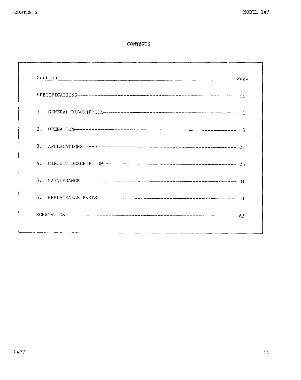
CONTENTS
MODEL 147
CONTENTS
Section
GENERAL DESCRIPTZON---------------------------------------------- 1
1.
OPERATION-------------------------------------------------------- 5
2.
APPLICATIONS----------------------------------------------------- 21
3.
C1I<CUIT DESCRIPTION----------------------------------------------
4.
MhINTENANCE------------------------------------------------------ 31
5.
REPLACEABLE PARTS------------------------------------------------ 51
6.
Page
25
SCHE~T~CS------------------------------------------------__-----__-- 65
0477
ii
Page 5

MODEL 147
igure
NO.
la.
lb.
2.
a:
5.
6.
7.
a.
9.
10.
11.
12.
13.
14.
15.
16.
17.
18.
19.
20.
21.
22.
23.
24.
25.
26.
27.
28.
29.
30.
31.
32.
33.
34.
35.
36.
37.
38.
39.
40.
ILLUSTMTIONS
ILLUSTNATIONS
Title
FrontPanel..
______-
.............................
Pag:e
1
Front Panel with Cable ......................... 3
Front Panel Controls .......................... 4
Model 147 Rear Pmel Controls & Connections. .............. 6
Model 1481 Low-Thermal Input Cable ................... 10
Model 1483 Low-Thermal Connection Kit. ................. 10
Bus System for Model 147 ........................ 12
Thermal Sink Construction.
.......................
15
Normal Wave Form at Demodulator with Input Shorted ........... 17
Wave Form at Demodulator Shown with Some Pickup. ............ 17
Wave Form at Demodulator when Amplifier is Saturated .......... 17
8-cps Filter Circuit for Recorder Output ................ 18
Using Model 147 with 4-Terminal Connections. .............. 18
Exploded View for Rack Mounting .................... 19
Circuit UsingGuildline9144 with Model 147 Null Detector ........ 21
Circuit Using Guildline 4363DL with Model 147 Null Detector. ...... 22
Circuit Using Guildline 9120 with Model 147 Null Detector. ....... 22
Circuit Using Biddle 605001 with Model 147 Null Detector ........ 23
Circuit Using Leeds & Northrup 7556. .................. 23
Circuit Using Model 147 Null Detector with ES1 240, 8OOR and KS 925. .. 24
Block Diagram of Model 147 Amplifier Circuits. ............. 25
Model 1.47 Tnput Circuit. ........................ 26
Diagranl of Power Supplies & Battery Charging Circuit .......... 29
Model 147 Input Compartment. ......................
32
Correct Wave Form in dc-to-dc Inverter ................. 36
Correct Wave Form in Oscillator Circuit. ................ 38
Improper Wave Forms in Oscillator Circuit. ............... 38
Correct Wave Form at Demodulator Test Jack ............... 41
Out-of-Phase Wave Form at Demodulator Test Jack. ............ 41
Top View of Model 147 Chassis ..................... 44
Bottom View of Model 1~47 Chassis .................... 45
Transistor Locations on Printed Circuit 76 ............... 46
Capacitor & Diode Locations on Printed Circuit 76. ........... 46
Resistor Locations on Printed Circuit 76 , ............... 47
Resistor 6 Test Point
Locations
on Printed Circuit 76. ......... 47
Resistor b Test Point Locations on Printed Circuit 74, Bottom Face ... 48
Component Locations on Printed Circuit 74, Top Face. .......... 48
Resistor & Test Point Location on Printed Circuit 75
Capacitor & 'Transistor Locations on Printed Circuit 75
Resistor Locations on RANGE Switch (5102). ...............
..........
.........
49
49
50
Resistor Locations on RANGE Switch (S102). ............... 50
i
0477
iii
Page 6
SPECIFICATIONS
MODEL 147
SPECIFICATIONS
iv
0477
Page 7

MODEL 147 NULL DETECTOR
GE:NLSAL DESCRIPTIOX
SECTION 1. GENERAL DESCRIPTION
l-1.
electronic null detector.
x
source resistance and 10 nanovolts with a
a power sensitivity of 3 x lo-21 watt.
GENERAL.
The Keithley Model 147 is designed specificaLly RS a col,vcnicnt self-contained dc
a.
Its sensitivity is 0.6 x LOT3 microvolt per mi.llimrter or 0.03
10-e
microampere per millimeter.
Its resolution is better tllnn 3 nanovolts with a LO-oll:il
300-ohm
source resistance.
This corresponds Lo
Zero shift is less than 15 nanovolts for sourcf
resistance changes from 0 to 300 ohms. Line frequency r~!jcction is better than 5OOO:l 011
its most sensitive range.
The Model 147 has 16 ranges from 30 nanovolts full scale to 1.00 millivolts on a
b.
zero-center meter. Meter accuracy is f2% of full scale on ~11 ranges.
For reliable and versatile use, the Null Detector is of solid-state design, cxccpi
c.
for the first two input stages. It has high line isolation - lOl(J ohms - and battery
or ac power line operation.
0572
FIGUPJ? La.
Front ,>anel,.
I
Page 8

GENERAL DESCRIPTION
MODEL 147
l-2.
grounding problems.
FEATURFS,
Battery operation permits complete isolation from ac power lines, eliminating many
a.
Battery operation also allows flexibility and convenience in use.
The Model 147 automatically recharges the battery if needed when the powercord is connected.
As an electronic null detector,
b.
the Model 147 is immune to mechanical vibrations.
It will also recover from a Z-volt overload on its inost sensitive range in less than 20
seconds.
c. Besides performing as a null detector, the Model 147 can also be used as a 2% direct-
reading nanovoltmeter.
The Null Detector has an output of ;tl volt at up to 1 milliampere for full-scale
d.
meter deflections to drive a recorder or oscilloscope. Output accuracy is ;tl% of full
SCSlS.
e. A zero suppression circuit,
furnishing up to 100 microvolts, permits measuring small
changes in a larger dc signal or compensating for thermal emf's.
l-3.
APPLICATIONS. (Also see Section 3.)
The Model 147 is designed specifically as a null detector. It has sufficient sensi-
a.
tivity to be used in most applications with all commercially available potentiometers, in-
cluding 6-dial models, ratio sets and resistance bridges, including Wenner, Wheatstone and
Kelvin Double Bridges. It can be used to make 4-terminal measurements.
Keithley's Model 147 is more sensitive than the finest galvanometer systems. It is
b.
also immune to mechanical vibrations,
thus eliminating the need for shock-free mountings.
Additional advantages over galvanometer systems'include the ability to recover from 2-volt
overloads in 20 seconds,
much less off-null loading, plus considerably faster speed of
response.
0572
Page 9
MODEL 147
CKNERAL DESCKIPTION
0572
Page 10

GENERAL DESCRIPTION MODEL 147
FIGURE 2. Front Panel Controls.
0572
Page 11
MODEL 147 NULL DlXI:C'l'OR
SECTION 2.
2-l.
line and the POWER SUPPLY Switch is in tile AC or OFF position,
charge current determines its brightness.
charged.
FRONT PANEL CONTROLS.
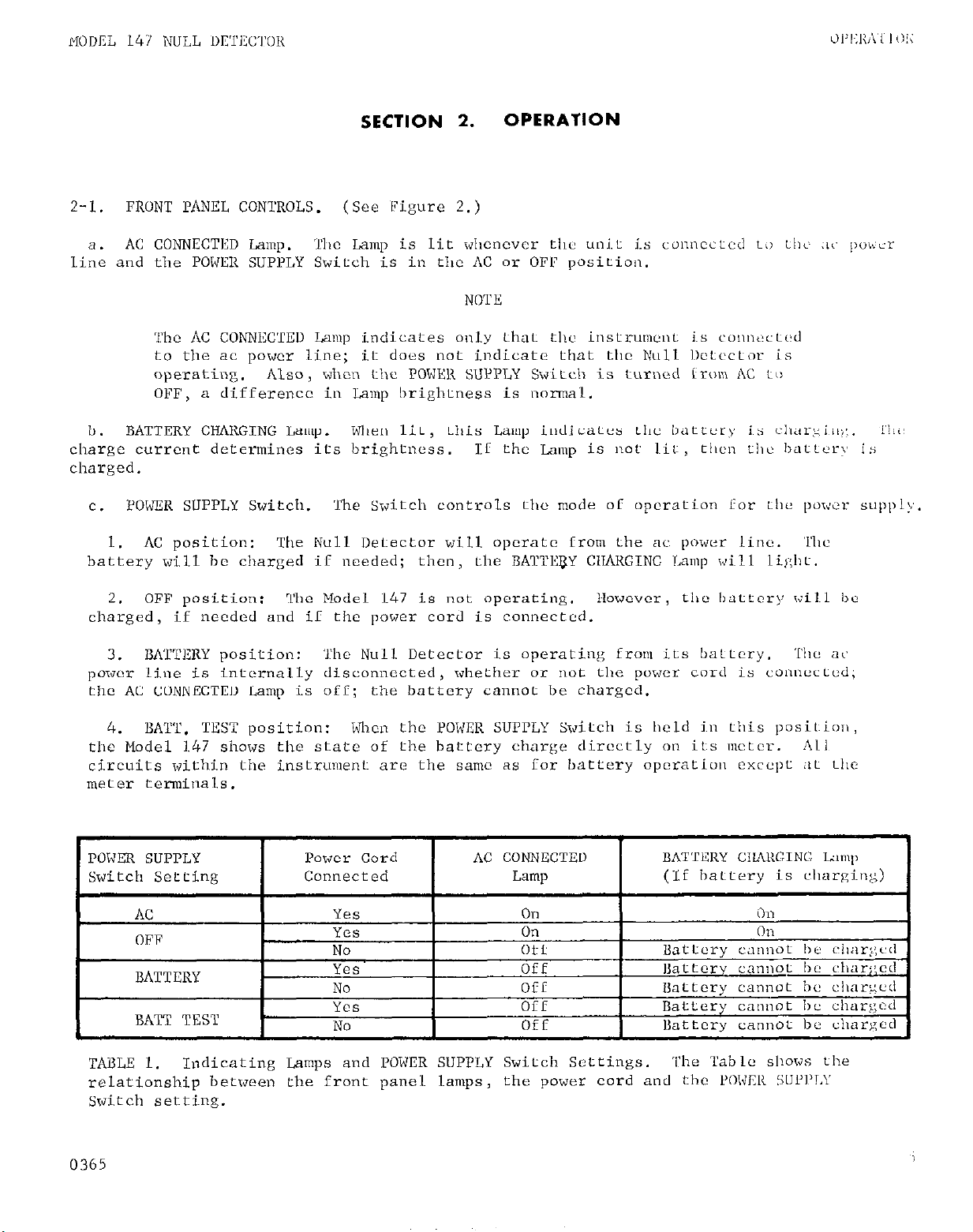
a. AC CONNECTI?D Lamp. l:hc Lamp is lit whcncvcr the unit is connected t0 i.lll xi. pwur
BATTERY CHARGING Lamp. When lit,
b.
POGJIZR SUPPLY Switch.
c.
AC position: The Null Detector will opcratc from the nc power Lint.
1.
battery will be charged if needed; then,
(See Figure 2.)
this Lanq indicates the ibattery ins clrnr:ini:.
Ihe Switch controls tlrc mode of opcratiori for tile powel- suppI!:.
OPERATION
NOTE
If the lamp is noi l~it,
the BATTEQY CIIARGINC Lamp will lil:ht.
tllc" LllC lbilCLtdl.\ ii
'TIIC
p1,:
OFF position:
2.
charged,
3.
power line is internally disconnected, whether or nut tile power cord is coluieclcd;
the AC CONNECTiXD Lamp is off; the battery cannot be charged.
4.
the Model I.47 shows the state of the battery charge directly on its mctcr.
circuits within the instrument are the same as for battery operation exccpl at Lllc
meter terminals.
POWER SUPPLY
Switch Setting Connected
if nccdcd and if the power cord is connected.
BATI'ERY position: The Null Detector is operating from its battery.
BATT. TEST position:
AC
OFF
BATTERY
BATT TEST
The Model 147 is not operating. Howcvcr ,
When the POWER SUPPLY Switch is held in this posil:ioii,
Power Cord AC CONNKTED
I
Yes
YCS
NO
Yes
NO
Yes
NO
Lamp
0”
On Oil
Off
Off
Off
Off
Off
I
tlic battery wil~l lbc
'I‘liC ni'
Al I
BATTERY CIIARGINC La"{'
(If battery is charging)
on
Battery CllnnOt bc cli;lr::c!d
Battfry cannot IbC char;:ed
Battery cannot hc chnr~cd
Battery can,,ot bc cllar~:cd
LIattcry cannot be charged
TABLE 1.
relationship between the front panel lamps,
Switch setting.
0365
Indicating Lamps and POWER SUPPLY Switch Settings.
The Table SllOWS tile
the power cord and the I'Oli'ER SUl'1~'I.Y
Page 12
OPERATION
MODEL 147 NULL DETECTOR
RANGE Switch.
d.
The RANGE Switch selects the full-scale meter sensitivity (either
microvolts or millivolts) for one of eight ranges, from 0.03
FUNCTION Switch.
e.
The FUNCTION Switch selects the function - MICROVOLTS or HILLI-
VOLTS - which is to be measured.
ZERO SUPPRESS Controls.
f.
The COARSE Control disconnects the suppression circuit (in OFF position) or
1.
Two controls determine
the
amount of zero suppression.
selects one of four suppression voltages in decade steps.
The FINE Control is a continuously variable adjustment for the suppression
2.
voltage set by the COARSE Control.
It adjusts the range between the positive and
negative values of the maximum voltage set by the COARSE Control.
INPUT Receptacle. The INPUT Receptacle is of a special low-thermal design.
g.
only the Models 14.81, 1482, 1486 and 1488 for mating connectors.
to
100.
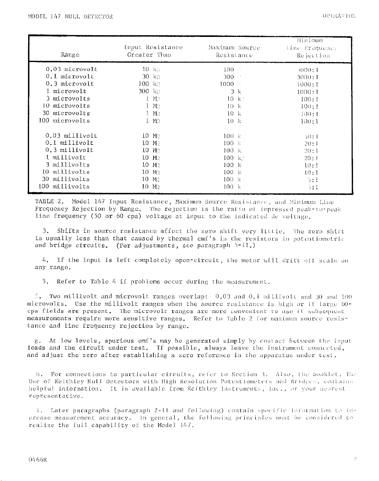
Refer to Table 3.
Use
FIGURE 3.
Model 147 Rear Panel Controls and
to Replaceable Parts List and schematic diagrams.
2-2.
RTtiR PANEL CONTROLS AND CONNECTIONS.
Line Voltage Switch. The screwdriver-operated slide switch sets the Model 147 for
a.
117 or 234-volt ac power lines.
Fuse.
b.
For 117-volt operation, use a 3 AG or MDL Slow-Blow l/@ampere fuse.
2.
For 234-volt operation,
2.
Power Cord. The 3-wire power cord with the NEMA approved 3-prong plug provides a
c.
ground connection for the cabinet.
use only a MDL Slow-Blow l/16-ampere fuse.
An adapter for operation from Z-terminal outlets is
provided.
6
Connections.
Circuit designations refer
0365
Page 13

MODEL 1~47 NULL DETCC'TOR
A note above the power cord shows the ac power line i:rcqucncy for
which the rejection filter is ad.justcd. 'The instrument will work
at any line frequency from 50 t" 1000 cps,
at the indicated frequency.
filter circuit.
NOTE
but ac rejection is bcsc
Paragraph 2-18 dcscribcs adjustirl~; lilf
DEMODULATOR TEST Jack.
d.
A phone jack provides access to LllE denl"dLll~ator ior ti.5:
purposes.
f.
OUTPUT.
'The OUTPUT Rcceptaclc provides
iL
volt at
one! mill.iampcrc f:or a
iilll.-scale
meter deflection on any range.
GND and LO Tcrmiasls.
f.
third wire of the power cord.
'The ground terminal. (GND) i.s conncctcd to tllc chassis ;~II)~! ! 1)~.
The low terminal is connected t" circui.t ground and cl!&:
low side of the input connection.
2-3.
MODE 01: OPERATION.
battery. b-or illost "SfS,
the ac power line will create ground loop or isolation problems.
The Model 147 operates cithfr irom an ac power line or irom iis
it functions well from ac. Use battary operation, llo~ifver, i~1~
1solnfi"n irun low to
ground is complete for battery operation when tllc power cord is disconnccl:cd; i,t is
greater than lOlo ohms wit11 the power cord connected.
Al.so use battery operntiiln it>
reduce the 8-cps ripple which may appear at the output with i-11" input shorted in i&c
operation.
See paragraph Z-16.
NOTE
Before using the battery operation, tll"r"ugllly read paragraph 2-4.
Improper battery "pcration can damage the battery pack and lead to
inaccurate measurements.
2-4. UXTERY OPERATION.
The Model 1.47 is supplied with a rcchargcablc h-volt,
ba:tery pack (Model 1489).
Recommended:
secutive hours without recharging.
Do n"t usf the battery more tlliln cigirt COII-
At this discharge rate,
4 ampere-ilour Iliclr~l-~~l(llnilIr!l
the battery sl10u1d last abOUt
1000 recharge cycles.
NOTE
Permanent damage to the battery pack occurs if it is used for more
than 16 consecutive hours without recharging.
rate, the recharge cycles are greatly reduced.
Model 147,
Cheek the battery charge before making a measurement.
b.
in the BATT. TEST position.
check the state of the battery charge.
The minimum acceptable charge is a meter indi.cntion oi ,8;
full. charge is shown by the BATTERY CHARGING Lamp not being lit.
At this discharge
Bflorf usi~ng tile
Hold the POWER SUPl'LY Switch
Recharge il needed.
Otherwise, battery operation is the same as for the ac power line operating mode; rcI:cr
to paragraph 2-5.
0365
Page 14

OPERATION
When the battery is used beyond its capacity, two effects aye seen.
There is a shift in zero offset from ac to battery operation.
the power supplies do not regulate and high ripple voltages appear
at the supply outputs.
MODEL 147 NULL DETECTOR
Also,
(See paragraph 5-8.)
To recharge the battery,
c.
POWER SUPPLY Switch to AC or OFF.
be charged only if needed, and the circuit automatically prevents it from being overcharged.
It is suggested that the battery be used during the day and be recharged at night.
d.
Leave the instrument always connected to the ac power line; then turn the POWEK SUPPLY
Switch to OFF at night. After a fully charged battery is used for eight consecutive
hours ) it will recharge within 16 hours.
effect on the isolation: 1010 ohms with the POWER SUPPLY Switch in BATTERY position and
the shorting link between GND and LO Te?.minals disconnected.
2-5. OPERATING PROCEDURES,
Set the front panel controls as follows:
a.
POWER SUPPLY Switch
FUNCTION Switch
RANGE Switch
ZERO SUPPRESS COARSE Control
Make sure the ZERO SUPPRESS COARSE Control if OFF. If it is not, a
suppression voltage is introduced, causing an error in measurements.
connect the power cord to an ac power line.
The BATTERY CHARGING Lamp will light.
Leaving the power cord connected has little
OFF
MILLIVOLTS
100
OFF
NOTE
Turn the
The battery will
Connect the voltage swrce or null circuit to the INPUT Receptacle.
b.
graph 2-6 for suggestions.
Check the voltage shown on the rear panel Line Voltage Switch; connect the Model 147
c.
to the ac pcwer line. Make sure the frequency shown above the power cord is the frequency
of the ac power line. At this point, the AC CONNECTED Lamp will light, asp will the
BATTERY CHARGING Lamp if the battery is being charged. If the circuit low is to be at
ground, put the shorting link between the LO and GND posts on the rear panel.
Turn the POWER SUPPLY Switch to the desired mode of operation, AC or BATTERY.
d.
Increase the Model 147 sensitivity until the meter shows the greatest on-scale de-
e.
flection.
1. Check the source resistance to make sure it is within the maximum value specified
for the range being used.
sitive ranges is exceeded, the Model 147 may not measure within its specifications.
2. Zero offsets seen when the Zero Suppress Controls are off will vary with the
quality of the circuit's thermal construction,
Shorting Plug is connected to the Model 147 INPUT Receptacle, offset should be less
than 0.3 microvolt.
8
(See Table 2.)
If the maximum resistance for the more sen-
See paragraph Z-14. When a Model 1488
Refer tO para-
046613
Page 15
Page 16
OP1:llATION MODEL I,47 NULL I1lYl'ECTOR
Make sure the signal is greater than Johnson noise in the source resistance (par-
1, ,
agraph 2-12 ).
2. Use materials which generate a low thermal emL (paragraph 2-14).
3. Mini.mize temperature changes and thermal gradients (paragraph Z-14).
4 Reduce magnetically induced signals by proper shielding and minimizing experimen-
tal layout area (paragraph 2-15).
5. Eliminate ground loops through proper grounding and connection to the signal cir-
cuit (paragraph 2-16).
2-6.
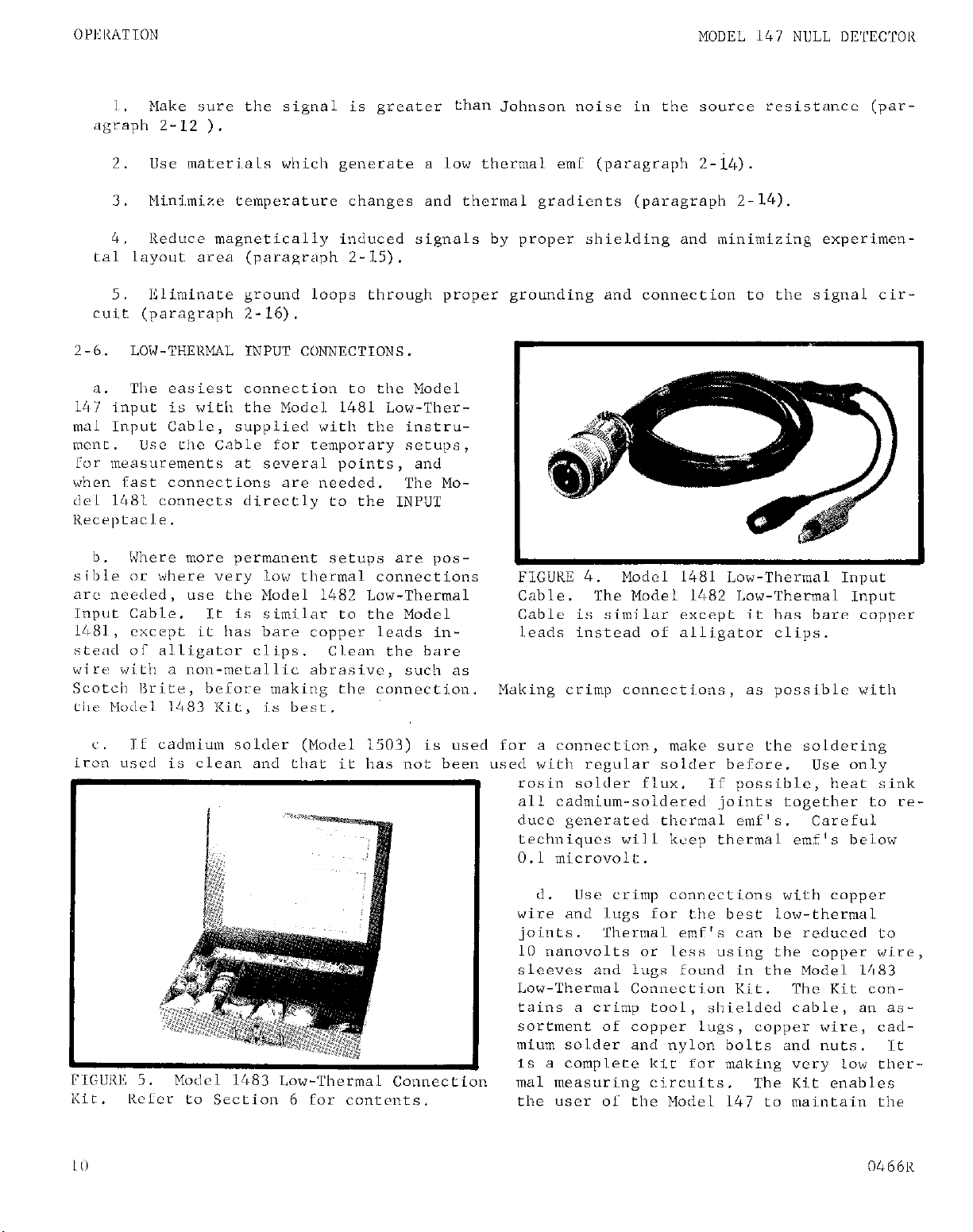
14~7 input is with the Model 1481 Low-Thermal Input Cable,
mcnt Use tile Cable for temporary setups,
for measurements at several points, and
when fast connections are needed.
del 148~1 connects directly to the INPUT
1~eceptacl.e.
sible or where very Sow thermal connections FIGUKC 4. Model 1481 Low-Thermal Input
arc needed, use the Model 1482 Low-Thermal Cable.
Input Cable.
1481 ,
stead of nl,ligator clips. Clean the bare
wire! width a non-metallic abrasive, such as
Scotch Isrite, before making the connection.
illc> Model 1483 Kit, is best.
iron used is clean and that it has not been used with regular solder before.
LOW-THEIMAL INPUT CONNECTIONS.
a Tlie easiest connection to the Model
supplied with the instru-
The Mo-
b. Where more permanent setups are pos-
'The Model 11+82 Low-Thermal Input
It is similar to the Model
except it leas bare copper leads in- leads instead of alligator clips.
('. Si cadmium solder (Model 1503) is used for a connection, make sure the soldering
Cable is similar except it has bare copper
Making crimp connections, as possible with
USC only
rosin solder flux. If possible, heat sink
all cadmium-soldered joints together to reduce generated thermal emf's.
techniques will keep thermal emf's below
0.1 microvolt.
Careful
I'LCUIW 5 .
K in t .
lieTcr to Section 6 for contents.
Model 1483 Low-Thermal Connecti
d. Use crimp connections with copper
wire and lugs for the best low-thermal
joints.
10 nanovolts or less using the copper wire,
sleeves and Lugs found in the Model 1483
Low-Thermal Connection Kit.
tains a crimp tool, shielded cable, an assortment of copper lugs, copper wire, cad-
mium solder and nylon bolts and nuts.
is a complete kit for making very low ther-
mal measuring circuits.
the user 011 the Model 147 to maintain the
Thermal emf's can be reduced to
The Kit con-
It
The Kit enables
0466K
Page 17

Page 18
OPERATION
MODEL 14,7 NULL DETECTOR
2-8.
line ground.
2-9.
range is $1 volt at 1 milliampere.
less than 5 ohms within the amplifier pass band.. Output may be used during both ac and
battery operation. If the Model 147 is used for differential measurements, do not ground
the recorder connected to the output.
FMATING OPERATION.
The Model 147 can be connected between two potentials,
a.
It can be floated up to ?4,00 volts off ground.
CAUTION
The front panel controls are electrically connected to the case.
power cord is unplugged,
ground voltage. use necessary e precautions.
For best results with floating operation, follow the steps below:
b.
Remove the shorting link from the LO or GND Post on the rear panel.
1.
Connect the input circuit to the Null Detector.
2.
2-5.
wfth this operation, since the low of the Model 14,7 output is no longer grounded.
better results.
The zero suppress controls may also be used.
If power line frequency pickup is a problem,
3.
KECORDER OUTPUT.
-
The Null Detector output for a full-scale meter deflection on any
the case may be at a voltage equal
Do not ground any recorders used
battery operation usually provides
Accuracy is ?I% of full scale. Output resistance is
neither of which is at power
If the
to
the off-
Operate as described in paragraph
Model 147
P
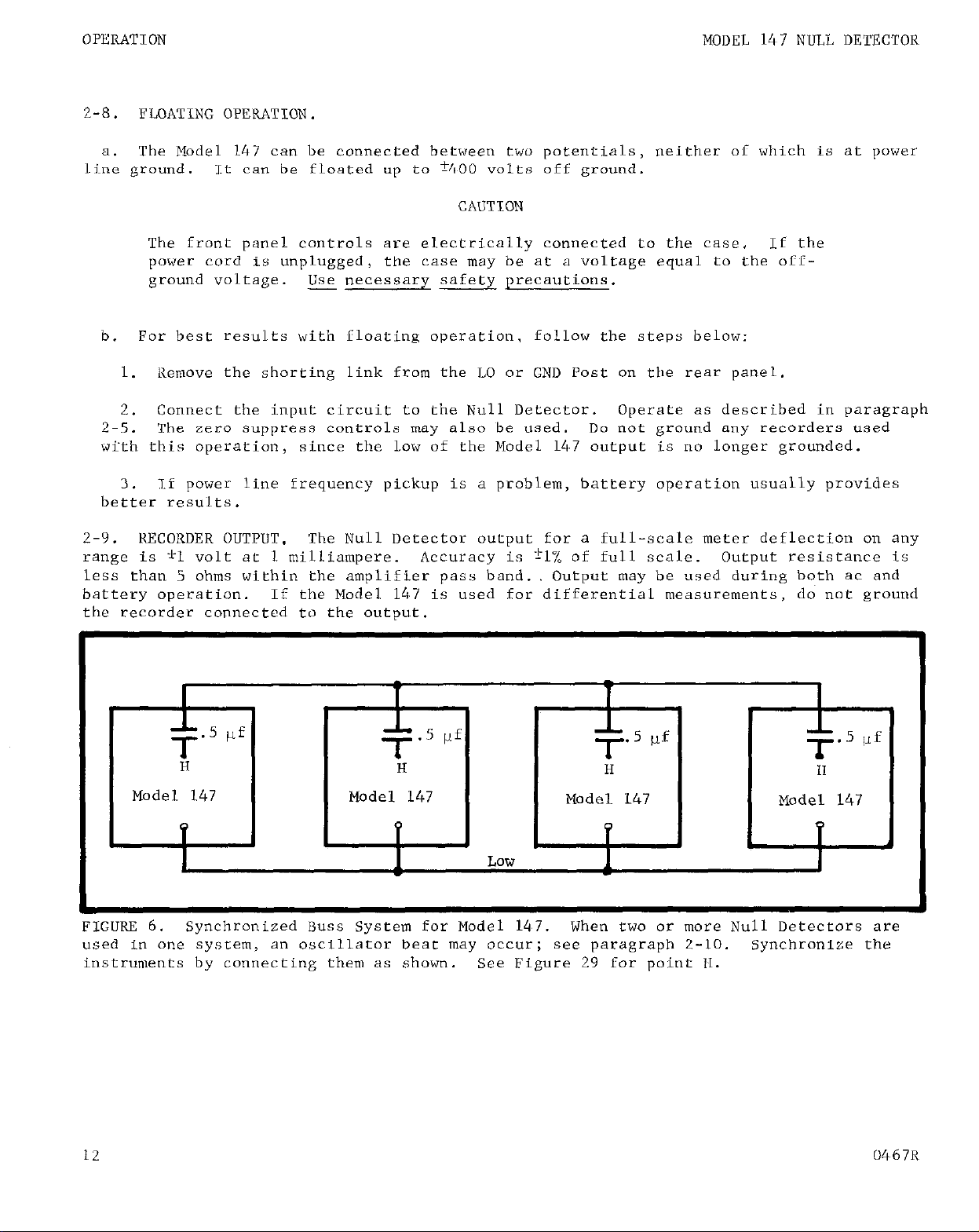
FlGURF 6. Synchronized Buss System for Model 14,7.
used in one system, an oscillator beat may occur; see paragraph 2-10.
instruments by connecting them as shown.
12
Model 147
V
Model 147 Model 147
v
LOW
When two or m"re Null Detectors are
See Figure 29 for point II.
b
4
Synchronize the
P
4
1
04,67R
Page 19

MODEL 1.47 NULL DETECTOR
2-10. USING MOIW THAN ONE MODEL 147 IN A SYSTEM.
The Model 1.47 oscillator is adjusted for a nominal freqnency ol 94 cps. ,,Oi.!i~VC~1 ~
a.
slight variations in frcqucncy do occur between models.
tectors in one system,
an oscillator beat may occur.
Wl,en using two or ,morc Xill I ill
Synchronizing oscillators
b.
"ents together at the collector of transistor (219 (Figure 29, Ipoint II), using iii: O.'i"icro.farad myl.ar capacitor.
At times the system is suc11 that the Null Detector lows may not bc conncctc~! di~-~~~t-
c.
ly together.
instruments. A IlO-volt,
farad isolation capacitor in seri~es with iboth pri~mary and secondary wi~ndin~s o! C!IE i~~:i,i::former.
For several Null Detectors connected together, l,sc a synct,r"ni~zcil bliss :;ysli'T!, :iii
d.
shown in Figure 6.
2-11.
other considerations beside tile instrument affect accuracy.
working with higher voltages are very important with mi~crovolt signals.
reads only the signal received at its input; tllcrciorc, it is i~mportant tllat this signal
be properly transmitted from the source.
affect accuracy: thermaI noise
connections.
ACCURACY CONSIDERATIONS. For sensitive measurcmcnts -
Then,
'Table 4 also offers a quick rcfcrence to correct troubles wllich may occ11r.
use a 1:l transformer havi~ng a fairly higil impedance between tllc Cvil
low power isolation transformer works wit.
prevents an objectionable beat. Connect tllc! cwc in:,t iii-
USC n 0..5-:nicr<v
10 mi~llivolts and bt~1lbi.x -
i:l:Ifcts not Iroticcnblc ,.i'!len
Tl,c, ~lodel vi 7
The fol,i~owing paragraphs indi~cate iactor xiii c:.
, input resistance, thermal emi's,
shi~cldilll: iin<l (. il(.l.: *
1. The thermal noi~sc in any ideal resistance can bc dctarmi~ned Srom tiic Joi~nson !~rlis~'
equation:
EZ",, =
where Erms is the rms noise voltage developed across the voltage source;
T is tile temperature in degrees Kelvin;
R is the source resistance in ohms;
F is the ampl~ificr bandwidth in cps;
k is the Boltzmann constant (1.38 x 10e23 joules / OK).
yor an ideal resistance at room temperature (3OO*K), equation 1 simplilics to
Ii,",
Peak-to-peak meter indi.cations are of "ore interest than tlrc rms vaiuc.
2.
mentally,
temperature, equation 2 becomes
where 13
0477
the peak-to-peak Johnson noi.se is about live times the rms value. At r<10111
EPP
is the peak-to-peak noise voltage developed across tile voltag" source.
PP
4 I< T 11 I; 1:q I
= 1.29 x lo-lo (RF)1'2 xi,
i:xpcri -
= 6.45 x 10-l' (RF)"' I:<,
Page 20
Very slow response time
Page 21
MODEL 147 NULL DETECTOR
2-13. INPUT RESISTANCE.
obtained using high feedback factors.
physical input resistance is partially destroyed.
exceed the maximum source resistance listed in Table 2.
but noise, offsets,
ranges, the maximum specified source resistance is consistent with Johnson noise considcrations.
2-14.
a.
tween any two junctions of dissimilar metals.
which the Model 147 can measure
b.
Model 147 can have some offset (paragraph 2-5).
touching the circuit, by putting a heat source near the circuit, or by a regular piliter,,
of instability,
light,
THERMAL EMF'S.
Thermal emf's (thermo-electric potentials) are generated by thermal gradients Ihe-
Thermal emf's can cause the following problems:
Meter instability or zero offset much higher than expected.
1.
Meter is very sensitive to ambient temperature differences.
2.
slow response and instability may result.
corresponding to heating and air conditioning systems or changes in sun-
The Model 147 is a feedback amplifier;
When the source resistance exceeds the amplifier's
amplifier input resistance without feedback - the fecdbacl;
Then the instrument may not operate properly.
Iligher resistances can be used,
These can be large compared to the si!;nals
its input resia:nnc<. is
Normally, do not
On the most sensitive
Note, thougll, the
T%is is seen by
To minimize the drift caused by thermal emf's,
c.
the same thermo-electric powers in the input circuit.
have o thermo-electric power within about f0.25 ,rv/oC of copper.
inbalance of 1oC between these metals would generate a thermal emf of about 0.25 microvolt
At the other extreme, germanium has a thermoelectric power of about 320 ,iv/oC, and silicon
will develop about 420 jrv/% against copper.
Standard physical handbooks contain tables
of thermoelectric powers of materials.
Since the Model 147 input circuit is made
of pure copper, the best junction is copper
to copper. HOWeVer, copper oxide in the
junction will cause thermal emf's on the
order of 100 nanovolts per oC or less.
Also, differences in processing of two
pieces of copper can cause thermal emf's
of up to 0.2 microvolt per OC. The Model
1483 Kit contains all necessary equipment
to make very low thermal copper crimp joints.
See paragraph 2-6.
Besides using similar metals, thermal
d.
emf's can be reduced by maintaining constant
temperatures, Keep all circuits from open
windows, fans,
similar sources which vary temperature. Connect leads or lugs as close as possible.
Minimize thermal gradients by placing all Separate only with insulation of high heat
junctions physically close on a large heat conductivity.
sink.
fore making a connection.
Thoroughly clean all copper leads be-
air conditioning vents and
Crimp together
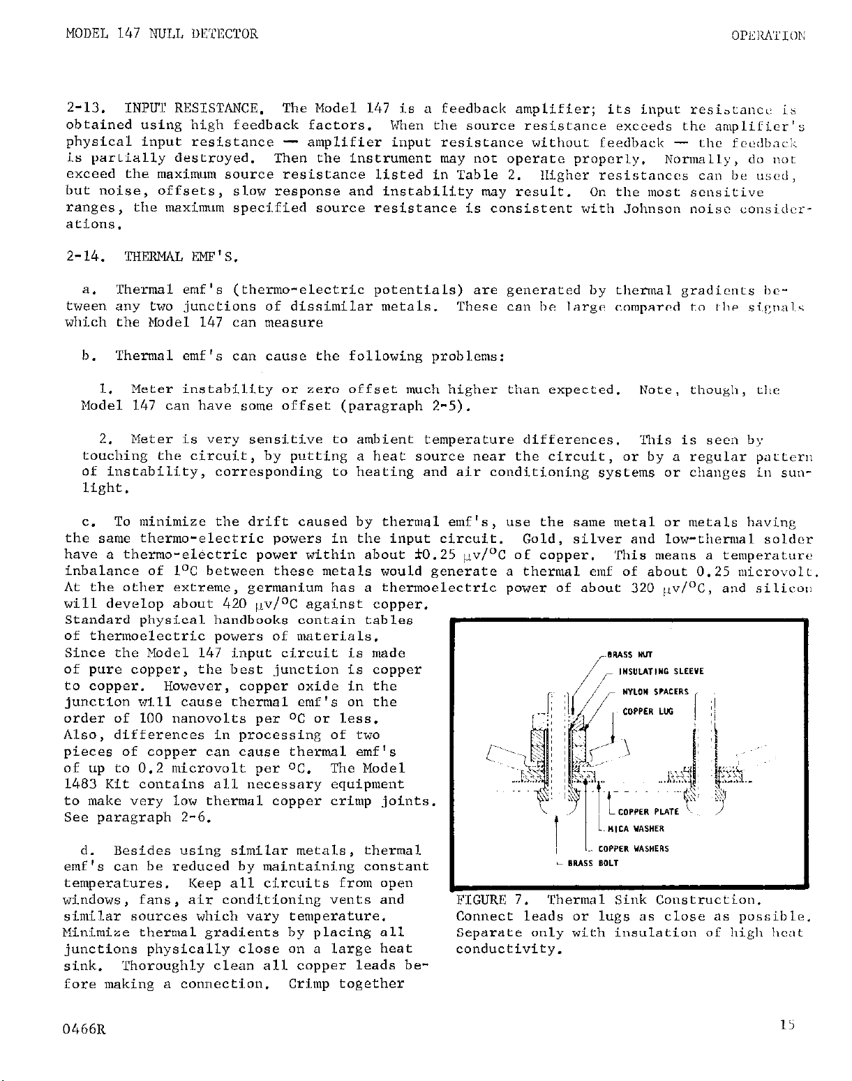
FIGURI? 7.
use the same metal or metals having
Gold, silver and low-thermal soldcr
This means a temperature
COPPER "AI"ERI
L Bw.II BOLT
Thermal Sink Construction.
1S
Page 22
OPERATION
MODEL 147 NULL DETECTOR
the ends of each copper wire;
bolt the lugs for each connection point together; mount all
stacks of lugs on a thick metal plate having high thermal conductivity. Thermal conductivity between the junctions and the heat sink can be kept at a high level by using mica
washers or high conductivity ceramics for electrical insulation.
Several other techniques will reduce the effects of thermal emf's.
e.
suppression circuit to buckout constant voltages.
If connections must be soldered, use
only cadmium-tin low-thermal solder, such as supplied in the Model 1483 Kit.
metals -
including regular solder -
well-controlled oil bath or a good heat sink is used.
may be used and low thermal emf's obtained if a
Thermal voltages may be calculated
Use the zero
Unlike
from the thermoelectric power of the materials in the junction and the possible temperature difference between the junctions.
z-15.
conductor can produce large signals compared to the instrument's sensitivity.
MAGNETIC SHIELDING.
a. In the
Low
resistance
circuitry
used with the Model 147, magnetic
Lines
cutting a
The amount
of signal developed is proportional to the area enclosed by the circuit and the rate of
change of magnetic flux. For example, motion of a 3-inch diameter Loop in the earth's
magnetic field will induce a signal of several tenths of a microvolt.
size of the Loop or moving it more rapidly will increase the signal.
Increasing the
Magnetic fields
from ac power lines will cause even more difficulty.
To reduce the effect of magnetic fields, use magnetic shielding. Where high ac
b.
magnetic fields are present, it may be necessary to magnetically shield the measuring
circuit , the unknown emf circuit or auxiliary equipment in the circuit. Magnetic shielding is available from
several
companies in the form of plates, foil or cable.
Twist input leads to minimize the area enclosed by the circuit loop,
c.
experimental Layout for minimum enclosed area is also of particular
Z-16.
a.
AC SHIELDING.
Due to its narrow bandwidth, the Model 147 is somewhat insensitive to ac voltages
value.
Planning the
superimposed upon a dc signal at the input terminals. However, ac voltages which are
large compared with the dc signal may drive the Model 147 ac amplifier into saturation,
erroneously producing a dc output at the demodulator.
Usually it is sufficient to connect
the cases of all apparatus in the measurement circuit together and ground at one point.
This provides a "tree" configuration, which minimizes ground
which all shields are connected should be as near as possible
Loops.
to
The common point at
the
circuit
ground of the
Null Detector at its input.
Improper shielding can cause the Model 147 to react in one or more of the following
b.
ways :
Needle jitter or instability,
1.
High offset (dc bias). Changing the power cord polarity or the connection between
2.
from 10% to 20% of full scale.
the LO and GND Posts may affect the amount of offset.
Slow response time, sluggish action and/or inconsistent readings between ranges.
3.
Amplifier saturation. Observe the wave form with an oscilloscope connected to the
4.
DEMODULATOR TEST Jack (Figure 3).
With the input shorted, it should approximate the
16
0466R
Page 23

MODEL 147 NULL DETiXTOR
----~
FIGURE 8. Normal Wave Form at Demodulator
with Input Shorted. Scale is 0.1 v/cm
vertical and 10 msec/cm horizontal.
o?'I:I?A'TION
wave form shown in Figure 8. If excessive pickup occurs, the wave Lorm will reseml,le
that of Figure 9.
The circuit will operate reasonably well as long as the wave form is
not clipped, as shown in Figure 10. At this point a dc offset is introduced.
To minimize pickup, keep the circuit away from ac sources. Shield as carcfullp as
c.
possible. Connect all shields together at the low side of the input or at the LO Terminal,
The voltage induced due to a magnetic flux is proportional to the arca of the loop. 'ThCSk-
fore, minimize loop arcas in the shield connections as
nect
the shield at only one point. Run all wires in the circuit along the same path, so
well as the
input circuitry.
CO,,-
the loop area is only the small difference in position of two adjacent wires.
Strong third harmonic magnetic fields - 180 cps for 60-cps units - may create an
d.
8-cps beat
possible nearby sources, such as heavy-duty transformers.
measuring circuit as far as possible from the magnetic field.
at
the Null Detector output and meter. To reduce this effect, turn off all
Remove the Node1 147 and the
If removal does not greatly
reduce the beat, magnetic as well as electrostatic shielding around the circuit ~nlny be
necessary,
For information concerning your particular shielding problem, contact Pcrl:cc-
tion Mica Corp., 1322 North Elston Street, Chicago, Illinois.
The 8-cps beat will be more apparent at the output terminals, since the meter is
e.
filtered. To minimize the beat,
USC the filter circuit shown in Figure 11.
the Null Detector's l-volt output at Eull scale to 10 millivolts.
duced by a factor of 1O:l.
If the 330 microfarads is objectionably large, increase rhc
resistor sizes by 10 times and use a 33-microfarad capacitor.
The 8-cps beat is re-
Since the recorder outpu;
This divides
0466R
Ii
Page 24

'OPERATION
is now only 10 millivolts, a non-polar capacitor is not necessary.
The Model 147 line frequency rejec-
f.
tion refers to the total ac voltage appearing at the input terminals, Therefore, the
Null Detector is affected by the sum of the
ripple in the working standard and the unknown source. Because of this, working
standards having high ac ripple components
will significantly reduce the amount of ac
voltage which may be tolerated in the unknown.
Model
147
MODEL 147 NULL DETECTOR
Shielding is preferable to input fil- FIGURE 11.
g.
ters. Resistive-capacitive filters add corder Output. If~tha 8-cps beat disturbs
noise (equation 1), and the resistance value the measurements, this circuit will reduce
must be subtracted from the maximum source the beat 1O:l.
resistance in Table 2. Inductive-capacitive
filters rend to create loop instabilities
within the Null Detector. Capacity alone across the input, however, is less Likely to
cause Loop instabilities,
2-17.
a.
cal connections will have on the potential being measured. IR drops, which in most circuits are insignificant, now become important.
a resistance of approximately 10 milliohms per foot.
6-inch length of this wire will produce five microvolts.
volt would mean using a wire 0.0006 inch long.
b.
be used to eliminate this error. Refer
to Figure 12.
c.
the zero suppress may be used to nullify
the voltage.
d.
the measuring system fluctuate, they will
develop fluctuating voltages which will
appear as noise or drift in the system.
CIRCUIT CONNECTIONS.
When measuring in the microvolt and nanovolt regions,
Four-terminal connections can often
If an unwanted IR drop is constant,
If the currents or resistances in
and it may be used to filter ac components in some cases.
For example, No. 20 AWG copper wire has
A l-milliampere current through a
FIGURE 12.
Connections.
8-cps Filter Circuit for Re-
consider the effect the physi-
To reduce this drop to 0.5 nano-
Current
3
Using Model 147 with 4-Terminal
Leads
Model 147
Leads
ii
t
2-18.
a.
Switch on the back panel (Figure 3).
Use only 250~volt MDL fuses.
b.
The Model 147 can operate satisfactorily from 60 or 50-cps sources, but the best ac re-
jection is achieved when the filter is set for the line frequency.
OPERATING FROM SOURCE OTHER THAN 117 VOLT, 60 CPS.
If the ac power source is 234 volts,
No other adjustment is necessary.
For 50-cps ac pave-s sources,
change the sideband filter capacitors, CL03 and C104.
use a screwdriver to change the Line Voltage
Change the fuse from l/8 ampere to l/16 ampere.
Use Keithley part
Page 25

MODEL 1.47 NULL DI:TL':CTOR
ClOS-.109M (C103) and C45-.0155M (C104) for 50 cps.
Refer t" Figure 32 for compon<!nt III-
cation.
2-19. RACK MOUNTING. (See Figure 13.)
The Model 147 is shipped for bench use with four
a.
feet
and a tilt-bail.
'i'hC :~i"dcl
4002 Rack Mounting Kit c"nverts the instrument t" rack mounting t" the standard i:I,\ (RL<I?-L\)
19-inch width.
To convert the Model 147, rem"vf the four screws at the bottom ot each sidii "1 t!~<!
b.
instrument case.
Lift off the top cover assembly with
To rem"ve the feet and tilt bail from the bottom cover assembly,
Item
(See Fig. 13) Description
1 cover Assembly
the
handles;
save c11e four SCi-fi”S.
turn the two scr(ii.:s Il<'ilT
Keithlcy
Part
No.
17162C
Qunntit!
I
2 Cover Assembly, Bottom (Supplied with
Model 147)
3
4
Angle, Rack
Screw, Slotted, lo-32 UNC-2x1/4 (Supplied
with Model 147)
5 Front Panel (Supplied with Model 147)
176950 1.
1462413
7
--4
---
1
TABLE 5. Parts List for Model 4002 Rack Mounting Kit.
@SCREW
/
i(j)FR PANEL
IGURE 13.
0466R
Exploded View for Rack Mounting,
Using Model 4002 Rack Mounting Kit.
19
Page 26

Ur'Diu~LUN
MODEL 147 NULL DETECTOR
the back.
The two pawl-type fasteners will release the cover and allow it to drop off.
Remove the feet and the tilt bail and replace the cover (2).
c. Attach the pair of rack angles (3) to the cabinet with the four screws (4) previously
removed. Insert the top cover assembly (1) in place and fasten to the chassis with the
two pawl-type fasteners at the rear.
Store the top cover with handles, feet and tilt-
bail for future use.
20
0466R
Page 27

MODEL 147 NULL DETECTOR
APPLICATIONS
SECTION 3.
3-l. GENERAL.
meters in null circuits, These are just samples of the circuits available and they do
not exhaust all the possible circuits. The setups which follow demonstrate how the Elodel
147 may be used.
3-2. WORKING SOURCES.
tage increment available on 6-dial potentiometers.
a stable battery working source with the potentiometer,
are generally limited by several inherent problems - instability, short-term noise of
several microwIts, pocr line regulation, and several millivolts of ripple,
ripple may produce dc voltage due to a slight rectifying action at connection points and
switch contacts. Also, working sources having high ac ripple components will significant-
ly reduce the amount of ac voltage which may be tolerated in the unknown. This is because the sc rejection of the Model 147 refers to the total ac voltage appearing at its
input terminals, and, therefore, is affected by the sum of the ripple voltages in the working BOUWB and the unknown source.
Follow the operating instructions in Section 2.
p~oints brought up in paragraph 2-11 and following,
ThFs section contains dfagrams using the Model 147 with various potentio-
The Model 147 permits resolution compatable with the smallest vol-
APPLICATIONS
When working at this resolutton, use
Line-operated working sources
This hig!I
NOTE
Pay particular attention to the
FIGURE 14.
KElTHLEY MODEL 147
POTENTIOMETER
Circuit Using Guildline 9144 with Keithley Model 147 Null Detector.
.-
GUILDLINE 9144
0466R
21
Page 28

AH'LICATIONS
MODEL 147 NULL DETECTOR
KEITHLEY MODEL 147
GUILDLINE 436301.
POTENTlOMETER
FIGURE 15.
Circuit Using Guildline 4363DL with Keithley Model 147 Null Detector.
KEITHLEY MODEL 147
“NXHOYH
GUlL DL /NE 9120
EYF
POTENT/OMETER
FIGURE 16. Circuit Using Guildline 9120 with Keithley Model 147 Null Detector.
22
0466
Page 29

MODEL 147 NULL DI:TIICTOR
Al?PI.ICATLoNS
FIGURE 17. Circuit Using Riddle 605001 with Keithley Model 147 Null Detector.
KEITHLEY MODEL /47
I
?
STD. CELL
em
000
r;;ir, isl
LttN 7556
POTENTlOMETER
,
FIGURE 18. Circuit Using Leeds & Northrup 7556 with Keithlcy Model 147 Null Ljctcctor.
1466
23
Page 30

APPLICATIONS
KEITHLEY MODEL 147
r
1
ITl I
D.C. GENERATOR ‘8 6 6
999
1 KELVlN RATIO BRIDGE p 0 1
I PPP,
I I
q’ ’
DETECTOR BOOR
ES./. 240
RESISTANCE
STANDARD RS 925
SD P
IO
80
f0
*ID 0
MODEL 147 NULL DETECTOR
24
0466
Page 31

MODEL 147 NULL DETKTOR
CIRCUIT DESCRIPTION
SECTION 4.
4-1.
a dc amplifier. Feedback is applied to the whole loop.
is amplified, demodulated, dc amplified and applied to the meter. A feedback network
samples the signal at the output and compares it to the input. The dc input signal and
the feedback signal are compared in the input transformer primary.
creases the voltage-difference signal between the two.
difference signal; line-frequency sidebands of the 94-cps signal arc filtered out.
ac signal is then demodulated by a saturated transistor switch and enters a dc amplifier,
which has a feedback capacitor to filter out the demodulator ripple. The dc amplifier
output is connected to the meter, the output terminals and the feedback network. Ihe
feedback resistors determine full-scale range. The zero suppress signal is conneclcd to
the feedback point in the input circuit.
GENERAL.
The Model 147 consists of a chopper, ac amplifier and demodulator systcim followed 1,::
a.
A mechanical chopper converts the dc input signal to a 94-cps signal. 'The 312 signal
b.
CIRCUIT DESCRIPTION
(See Figure 20.)
'The transformer in-
The ac amplifier amplifies the
Th<!
FIGURE 20.
The power source for the Model 147 is either line voltage or the rechargeable
c.
battery.
highly regulated supplies.
amplifier circuits.
it is necessary and when the line voltage is connected.
4-2.
a.
JlOl, to the center contact of the chopper, GlOl. (See Figure 21.)
0466~
Voltage from either source is applied to a dc-to-dc inverter and then to tnrec
There is also a battery charging circuit to charge the battery when
Refer to Schematic Diagrams 18512F, 17352D and 173531) for circuit designations.
INPUT CIRCUIT.
The dc input signal is connected through the high terminal of the INPUT Receptacle,
Block Diagram of Model 147 Amplifier Circuits.
The three supplies furnish power to the oscillator and the
NOTE
The feedback signal
25
Page 32

CIRCUIT DESCRIPTION
MODEL 147 NULL DETECTOR
r
.
*
FIGURE 21.
The feedback signal, Vf (the dc amplifier output voltage, Vo, times the feedback ratio,
B )l
is the difference between the two, Vd = Vin - Vf.
applied to the Model 147, Vf is zero and the voltage across the primary is entirely Vin.
As the output voltage rises,
"in,
determines the amplifier gain.
is applied to the center tap of the input transformer, TlOl.
applies a positive and a negative square-wave signal across each half of the primary.
The magnitude of the square wave is proportional to the difference between the dc input
and the feedback signals.
internal ac pickup.
is applied to the transformer primary.
Or p V, = Vin.
The input compartment is designed to insure high thermal stability and to minimize
b .
1. .
circuitry.
input receptacle is 99.5% copper; the impurities add to the mechanical strength without
creating large thermal emf's.
copper pins and rotor.
lugs.
soldering -
Model 147 Input Circuit.
Vf fncreases and Vd decreases to a small value, then Vf =
Only p, which depends upon the RANGE and FUNCTION Switch settings,
TlOl steps up this signal and applies it to the grid of tube Vl.
Thermal stability is obtained in part by using only copper wire in the input
The input transformer primary and the chopper leads are pure copper.
The low voltage portion of the FUNCTION Switch uses pure
All connections to components are made with pure copper crimp
Connections between components are made by bolting the lugs together - not
to reduce thermal emf's.
The dc input signal, Vin, is applied to the chopper.
The signal, Vd,
When the dc input signal is initially
stepped up by the transformer
'The chopper alternately
The
.
2. The input compartment is doubly shielded against magnetic and electrostatic
pickup on all sides.
further minimizing pickup.
c. The feedback network is formed from the output of the dc amplifier back to the
center tap of the primary of transformer TlOl.
feedback ratio used for each range.
4-3. AC AMPLIFIER.
a. The ac amplifier circuit amplifies the 94-cps difference signal which corresponds
76
The wires are physically placed to maintain minimum loop area,
The RANGE Switch, SlO2, selects the
0466R
Page 33

MODEL 147 NULL DETECTOR
to the dc input signal.
The signal is applied to the grid of tube Vl and further ampli 1 ic'j;
by tube V2. A low-noise silicon transistor, Q3, provides n hi.gb impedance load frx \':i.
The signal is then amplified by transistors Q4 and 00. Potentiometer I<109 , botwe~~l tiie 03
emitter and Q4 base, adjusts the gain to compensate for beta variations. In addi~cioii ,
each stage has some local degeneration.
Transistor Q5 is for impcdancc matchi~n):. 'I‘ll i!
difference signal is amplified by transistors (27 and 98, whicll also form ii full-vavc
signal for demodulation.
A series high-Q filter
b.
from
the plate of V2 to circuit ground provides riotit, rcjection at the power-line frequency sidebands. 7'11e values of capacitors Cl03 and i:l(lt+
depend upon the power-line frequency. Due to the high Q of the inductor, the iil,ter
forms sharp notches at 34 cps and 154 cps for 60-cps power lines and 44 cps and 144 cps
for 50-cps power lines.
'The ac amplifier's 94-cps gain and phase characteristics al-c
affected very little.
The tube type and bias point of Vl are selected for low-noise operation at 94 cps.
c.
The high-Q tuned circuit in the plate of Vl has a good signal-to-noise ratio, and it
provides a narrow bandwidth around 94 cps.
The tuned circuit's Q is lowered on tile
higher ranges for amplifier stability.
4-4.
DEMODULATOR. Transistors Q9 and QlO in inverted configuration form a trnnsislor
switch demodulator. 'They convert the 94-cps wave from the ac amplifier into a dc vo1ca~:i
with ripple component. Resistors R123 and R124 sum the voltages from each to form rl lullwave rectified signal. Jack J102 allows access to observe the wave form.
'i‘llI 94-cps
oscillator furnishes a square-wave drive for the demodulator.
4-5.
DC AMPLIFIER.
The demodulator signal is amplified by two low-drift, high-gain silicon transistors,
a.
Qll and Q12, in differential configuration to compensate for temperature drift. Transis-
tors 413 and Q14 form the second amplifier stage. Total gain is about 500.
follow
current at zero output.
output stage
-
transistors
Q15 and 916 in pnp-npn configuration - draws litclc
Diodes DlOl and D102 limit the output currCnt, protecting
'The emitter-
transistors Q15 and Ql6.
A feedback loop with capacitor Cl15 around the dc amplifier acts as an integrator,
b.
filtering the ripple component of the demodulated wave form, The effective capacity,
which is approximately the value of Cl15 times the dc amplifier gain, and the feedback
factor (or open-loop gain) determine the response speed of the system.
The capacitive
feedback also lessens the noise in the amplifier outside the system bandpass.
4-6. OSCILLATOR. The oscillator circuit, stable to 0.1 cps, has three parts: phase-shift
network for a 94-cps signal, an amplifier to drive the chopper,
and a transistor switch
and phase compensation network for the square-wave demodulator drive.
The phase-shift network consists of capacitors C301 through C303, resistors 11319
thzough R321, and the combined resistance of R303 and R318, which bias transistor Ql7.
The input impedance of the emitter follower,
tive value of this last resistance.
Transistor Ql8 compensates for signal losses in the
phase-shift network. Potentiometer R319 adjusts the signal frequc?ncy.
the filament of a low-power subminiature tube, Raytheon CK544,
417, has little loading effect on the effec-
Resistor 1~322,
provides variable dcgcn-
eration to maintain a sine wave output to the amplifier.
0365
27
Page 34

CIRCUIT DESCRIPTION
From the phase-shift network, the signal is amplified and used to drive the chopper.
h .
'Transistor 919 matches the impedance of transistor Q20 to the phase-shift network.
tentiometer
R313 adjusts the signal amplitude.
From transistor 420; the signal is applied
MODliL 147 NUL,L DIXECTOR
PO -
to the primary of tratwformer T301, which drives the class B stage, transistors Q22 and
Q23.
After amplification the sine-wave signal is applied to the chopper, GlOl. Transistor
Q21 develops the bias voltage for the class B stage, providing ambient temperature compensation for the chopper-drive signal amplitude. The center taps of transformers 'T301
and T302 supply dc current for the class B stage.
c. 'The chopper drive signal is also applied to the primary of transformer T302.
The
transformer drives transistors Q24 and Q25 through a phase-compensating network, resistors
R308 to R310, R323 and capacitor C309, which compensates for the chopper phase shift.
the transistors alternate between saturation and cut off to form a square-wavt? drive for
the demodulator, transistors Q9 and QlO.
4-7. ZERO SUPPRESS.
The zero suppress circuit provides a regulated voltage from the power supplies to
a.
buckout steady background potentials in the input signal. The IO-turn FINE Control,
potentiometer
R168,
is connected between -12 and -1-12 volt outputs.
The resistors I~165
to R167 and R172 in the COARSE Switch, S103, further divide the voltage. The suppress
voltage is divided by an Evenohm 0.25% resistor, R140, copper resistor Rl37A, and copper
resistor R141. Using copper resistors for the lowest voltage points shunted by Evenohm
resistors provides thermal and resistive stability.
An adjustable current, supplied through resistor R138, provides compensation for
b.
resistive
4-8.
offset. Potentiometer R239 adjusts the current fed to the feedback point.
POWER SUPPLIES (See Figure 22.)
The power supply for
the
Model 147 ,is powered by
an unregulated supply :from the line voltage or rechargeable battery. Either source feeds
n dc-to-dc inverter and three highly regulated supplies with outputs of +12, -12, and
il.2 volts.
The line voltage, battery and battery charging circuit are controlled through the
a.
POWER SUPPLY Switch, S201. When the switch is in AC,
These power all the other Model 147 circuits.
the battery is charged if nccessarq
and the power supply uses line voltage. When the switch is in OFF, the battery charging
circuit
will operate if necessary; all other circuits are off.
When the witch is in
I~ATTIZRY, the power supply uses the battery; the other two circuits can not operate.
11 . T:he unregulated supply consists of a full-wave rectifier, diodes DZ.12 and D213, and
n droppi.ng resistor, R232.
The AC CONNECTED Lamp,
DS201, is in series with resistor R226,
whj.ch is connected directly across this supply, For battery operation the primary of
rrnnsl'onner T201 is disconnected.
c.
Voltage
Vertex circuit.
voltage to transformer T202.
carrier frequency.
from the unregulated supply or the battery is applied to the dc-to-dc in-
Transistors 928 and Q29 form a switching network to supply an interrupted
The switching frequency is about 2 kc, well away from the
Transformer T202 has a
saturable
ferrite cot". The inverter
circuit
supplies voltages to the three regulated supplies, which are basically the same series
regu.Lator
d . For the 1~12 volt supply,
i-rnnsfonncr T202.
is div:idcd by resistors R208 and R209 and compared L
28
design.
diodes D206 and D207 full-wave rectify the signal from
The signal is applied to the pass transistor, Q30.
the zencr diode reference, D205.
The output of Q30
0466R
Page 35

MODEL 147 NULL DETECTOR
CTRCUIT I1I:SCR1~l"~IoN
FIGURE 22.
Block Diagram of Model 147 Power Supplies and Battery Clrarging Circuit.
Transistors Q34 and Q33 amplify any potential difference and apply a signal to the base
of transistor Q32.
collector voltage of Q33 directly dctcrmincs the current through (132, which comes
the -12 volt supply.
the base of transistor Q31,
junction.
Diode D203 limits the base-to-emitter voltage of the Q30 alld Q3L combinati,ln;
thus also limiting the current which it will pass.
Diodes 0204 and D205 fix the emitter voltage of (~32; tlrcrclfore, the
i:rom
The
current
and therefore the
drop through
resistor I<216 determines the voli~a?ge at
output
voltage througli the base-cmiltcr
Diode I)203 protects
the
pxs transistur
Q30, if the output of the supply is shorted.
For the -12 volt regulated supply,
e.
from transformer T202.
The signal is applied to the pass transistor, Q35.
R217 and R218 divide the 435 output,
ground as a reference.
apply a signal. to transistor Q37.
Transistors Q38 and 939 amplify any potcutial diftcrc!ncc and
Transistors 435 and Q36 form a Uarlillgton combi~n;lLi~x,~i ~
and work similarly to that in the ~1+12 volt supply.
supply draws a higher current than the ~1.12 volt supply,
D208 and U209, to protect the pass transistor.
diodes D210 and D211~ Trill-wave rectify the signill
Resistors
thereby comparing it to the ~112 volt supply, usi,n>:
'l'hc differences arc
LIlaC Clue -12 volL
and therefore uses two diodes,
The negative "bootstrap" curreni supply)
is from a filter, resistor R225 and capacitor C210.
The -+I..2 volt supply operates in the same manner as the 112 volt supply with those
f.
di,fferences. The output of the pass transistor, Q40,
1~1.2 volt supply divided down one
tenth.
'The operating voltages for tlic comparator stage,
Q43 and Q44, are obtained from the +12 and -12 volt supplies.
is compared to lllC output of ti1c
ikccpt for the compnra~or
stage, npn transistors arc used.
4-Y.
BATTERY CHARGING CIKCUIT.
The battery charging circuit operates when the I'OWER SUPPLY Switcii, SZOI, ins iii A(:
a.
or OFF position, and only when the battery needs charging.
04661~
29
Page 36

CIiWJIT DESCRIPTION
The battery voltage is compared to a reference by two cascaded transistors, Q26
b.
and 427.
When it is low, a charging current from transformer T201 is applied to the battery
MODEL 147 NULL DETECTOR
through the BATTERY CHARGING Lamp, DS202, transistor Q27 and diode D216. The reference
is zener diode D214; the reference voltage is adjusted by potentiometer R228. The
difference between the battery and the reference potentials determines the magnitude of
the charge current through Q27. A silicon diode, D216, prevents the battery from being
run down because of leakage currents through 927, a germanium power transistor.
Diode
D215 limits the base-to-emitter voltage of the Q26 and Q27 combination, so no more than
400 milliamperes (the rated maximum charge current of the battery) can flow in the circuit.
This circuit protects the bat,tery. It decreases the charging current to a trickle-
c.
charge rate as the battery terminal voltage approaches the reference voltage. It also
limits the charge current if the battery was used beyond its ampere-hour capacity. Note,
however,
reversal of a cell may occur,
that the battery can be damaged if it is used far beyond its capacity. A polarity
causing heavy circulating currents within the battery.
30
0365
Page 37

MODi?L 147 NULL DIZECTOR
SECTION 5.
5-l.
cedurcs for the Model 147.
possible to maintain the instrument's specifications.
5-2.
high-quality electronic equipment.
Principal maintenance is an occasional chopper rcplaccment.
GENERAL. Section 5 contains the maintcnancc, troubleshooting and calihmtion pro-
It is recommended these procedures be followed as c:loscly 3s
MAINTENANCE SCHEUUJX.
The Model '1.47 requires no periodic maintenance beyond the normal cnrc requirc.d ~1
a.
Components operate well below nmximum ratiirgs.
Suggested Model 147 calibration schcdulc is as follows:
b.
Every four to six months, cl~cck the Model 147 with Llle Keithley Model. 260 N;li,a-
1.
volt source. This will show if the Null Detector is maintaining its specified accurac;?.
Approximately every year, perform an operational check on the amplifiers (par-a-
2.
graph 5-10). This will indicate how well the Null Detector ,is operating.
3. Normally,
are replaced.
the Model 147 does not need recalibrating unless critical components
These part changes are call.ed out by the various circuits in tliis Section
MAINTENANCE
(See paragraph 5-4.)
5-3. PARTS REI'MCEMliNT.
a. The Replaceable Parts List in Section 6 describes the clcciriccil components of :h~
Null Detector. Repl.ace components only as ncccssary,
which meet the specifications.
R322, which is a subminiature tube filament,
matched transistors (Qll, Q12, Q22, 423) and the two input tubes.
coded 80164 in the Replaccablc Parts List arc purchased only from Keithley Ins~run~cnts
or its representative. (If tlic Low-Tlicrmal~ Function Switcll, 5101, i,i?<!dS L^<~!/>l:,cme,,L, ri'-
turn the unit to i(eithtcy :Instrumcnts for this repair).
Component
Battery pack assembly
Mechanical chopper assembly (SW paragraph 5-4.)
Input receptacle assembly
Copper feedback resistor assembly R137
Evanohm resistor assembly
i:vanoh~n resistor assembly
Function switch plate assembly (see paragrnpll 5-3n)
Input transformer assembly
The Model 147 uses few special parts except for resistor
the components listed in 'Table 6, several
and USC onl~y rcliabltl replncements
mke S"lf parLs
BA201
GlOl
JlOl
11139
Rl40
SLOl
'SlOl.
TABLE 6.
and the proper lead length.
instructions given in paragraph 5-3.
04691~
Model 1.47 Pre-assembled Components.
USC only Kcithley parts for replaccmcnts;
Tlicsc parts have lugs crimped on Lhcm
iolloi;
Page 38

MAINTENANCE
>IOtII:L 1~11~7 NULL I)ETECTOR
I
FIGURE 23,
placing, duplicate location and order of lads on posts.
nations.
The physical location of components in the input compartment is critical.
11 .
rcpl.acement parts in 1-11~ exact pos:i.tion shown in Figure 23.
extraneous ac signals; see paragraph 2-15.
posts greatly affects offset and noise in the Model 147.
cnch lead as it is removed.
6 Kep nuts in the input compartment is 15 inch-pounds.
No .
ili~ich have lugs crimped on them. When replacing these parts,
metallic abrasive,
~Vol~low the procedures necessary for good low-thermal connections.
5-4. CHOPPER REPLACLWi?NTS.
The chopper is designed ~Cor long lift. I~l"wfvcr) since iC is mechanical, it will
ii
eventually wear and become noisy. At this point,
Removal Procedures.
11 .
1.
move the three thumb screws in the input compartment and the three chopper lead lugs.
Model 147 Input Compartment.
Refer to Figure 7 for general connection construction.
Replace in reverse sequence.
such as Scotch Brite, found in the Model 1483 Kit, or its: equivalent.
Llisconnect the chopper dri.vc coil at connector 5302 (Figure 29).
Note exact physical Location of parts. If re-
Figure 30 gives circuit dcsig-
Circuit loops will introduce
The order of the copper lugs on the insulated
'Tag or record the number on
Maximum torque applied to the
Table 6 lists components
clean the lug with a non-
replacement is necessary.
Carefully re-
I
Place
:1 2
0466R
Page 39

MODEL 147 KLILL DEl:CC:COR
:.?,\~I !:'I i ::,:'..::I
Carefully slide the degaussing coil, 1.302 (t?igurc 29),
2.
l'rom ti,(i chopper lbd~:;
remove the "1.d chopper.
Replacement Procedures.
c.
Slide the degaussiug coil,
1.
L302 , over the new chopper body irom illc bo!~c,!ll.
Orient so that tllc cut-nrit i.n I-11" coil lits over the ch"ppcr dri~vi! l~cnd.
Mount the chopper and coil in the input compartment.
2.
i)rcss Leads as silLlw:l
in Fj.gure 23.
Degaussing Coil Adjustment Procedures.
d.
With the input shorted, USC the ZERO SUPP1~L:S.S Contrill~s L:" cance 1~ any T/~e~livil~
1.
emf's in the Model 147 input circuit.
USC n differential input LU tile .Cypc 1103
Oscilloscope (~I and - inputs) to obscrvc the wave Lorm bctwecn tllc: collectors oi irai:sisters Q9 and QlO (Points P and Q, Figure 34).
The wave form amplitude varies as tllc degaussing coil is moved along the clltipper
2.
body. Potentiometer R301 (Figure 30) determines tbc effect "f the coil "n the wvc!
form.
Adjust both tbc coil and the potentiometer for mini.mum ;ImpliLudi,.
,:<~Lii~~l-sL
the.rcd and black leads t" the degaussing coil ir necessary.
3. An 8-cps beat at points P and Q may bc present.
USC battery operalion i" ~-c<!ucc
the beat; refer to paragraph 2-3.
5-5. 'TROUBLESHOOTING.
1%~ following procedures give instructions for repairing troubles which mii:ht occ111'
a.
in the Hodcl 147.
mcnt parts.
'Table 7 lists equipment recommended for troubleshooting.
cannot be readily located or repaired,
Use these procedures to troubleshoot and use only spwil:j~w! rcplacc-
cOntact Kcithley Instruments or its 'cl'~~scnl;li:ii,et-
Paragraph 2-19 describes how to remove the Null Detector covc1'.
Paragraphs 5-8,
b.
checking "ut the pow"r supply,
order given. Tables 10,
refer
to
Section 4 to find
The Schematic Diagrams,
5-9 and 5-10 give step-by-step proccdurcs for trouh1L'sho"iin;: arid
oscillator and amplifier circuits.
11 and 13 are troubleshooting tables for these circuits.
the
more crucial components and to detcrminc their iunclioi!.
1.8512F, 17352D and 17353D, contain the voltages at certai~n
pojnts in the circuit.
Before troubleshooting inside the Model 147,
(paragraph 5-6).
Always check out the power supply and the "sci.lI.at"r
circuits before touching the amplifier circuits.
check the extfrnal circuits
'I?," amplifier circuits
often appear faulty only because of a defect in the power suppty or
oscillator circuits.
11 Lllf L~I:oLIl~ II
Follow these in i~!lC
Xl so
0466R
Page 40

MAINTENANCE
MODEL 147 NULL DETECTOR
Instrument
llewlett-Packard Model 5512A Electronic
Monitor oscillator frequency
USC
Counter, 300-kc counting rate, *O.l%
accuracy
Keithley Instruments Model 1488
Short INPUT Receptacle
Low-Thermal Shorting Plug
Keithley Instruments Model 260
Signal source for calibrating Model 147
Vanovolt source
<cit%ley Instruments Model 2603
Connect Models 147 and 260
Low-Thermal Input Cable
(eithley Instruments Model 660 or 660A
Check voltage at output terminals
3-uarded DC Differential Voltmeter,
!-O.OZ%, to 1 millivolt
XA Model WV98B Senior Voltohmyst, 11 I$]
Check dc voltages throughout circuit
input resistance, i3% accuracy, 0 to
1500 volts dc
Cektronix Type 503 Oscilloscope, dc to
'I,50 I--
Check wave forms for troubleshooting and
-alibrating
I
TABLE 7. Equipment Recommended for Troubleshooting and Calibrating the Model 147.
these instruments or their equivalents.
use
5-6. PRELIMINARY TROUBLESHOOTING PROCEDURES.
Before troubleshooting,
a.
check the outside circuits to the Model 147.
Null Detector from all external effects:
Disconnect all outside circuits from the INPUT and OUTPUT Receptacles, and GND
1.
and LO Terminals.
Connect the Model 1488 Shorting Plug to the INPUT Receptacle.
2.
COARSE Control to OFF,
If battery operation is trouble free, set the POWER SUPPLY Switch to BATTERY.
b.
connect the power cord from the ac power line.
earth ground or to a cornman test equipment ground.
NOTE
Often, after checking out according
to
will function normally. This points to problems in the circuits
outside the Null Detector. Refer
to
Table 4 to check the external
circuit,
C. If ac operation is used,
check the Line Voltage Switch for correct position and the
Fuse for correct rating.
Isolate the
Set the ZERO SUPPRESS
Dis-
Ground the Model 147 case to a convenient
paragraph S-6, the Model 147
34
0466R
Page 41

COlltrOl
Dcsig. Kcf.
Paragraph
ac amplifier gain adjust
R109
34
5-10
Imeter adjust
battery charging adjust
current compensation adjust
dcgaussing coil compensation
oscillator amplitude adjust
oscillator frequency adjust
TABLE 8.
Model 147 Internal Controls. The Table lists all internal controls, the
figure picturing the location,
5-7.
CHECK OUT AND CALIBRATION PROCEDURES.
The following procedures give the steps to check out and calibrate the Nod"1 147
a.
R228
I~239
R301
R313
R319
I
I
36
29
30
37
37
and the paragraph describing the adjustment.
5-8
5-11
5-4
5-9
5-9
circuits. If a circuit fails to check out at any point, refer to the circuit's trrxll)l<-shooting table. Continue as long as the points check out. Use the equipment l~istcd in
Table 7.
Procedures arc given for the power supply,
b.
oscillator and amplifier circuits.
These cover the principal adjustments t" bring the instrument within specifications.
If the Model 147 is not within specifications after performing these checks and
c.
calibrations, contact Keithley Instruments or follow the troubleshooting proccdurcs io
find the fault.
NOTE
Make sure the power supply and oscillator circuits are operating
correctly before chcckin~ the amplifiers. All circuits dcpcnd
upon properly functioning power supplies.
If taken out of order,
the resulting adjustment may be faulty.
5-8.
outputs
check out at any point, refer to Table 10.
POWI?R SUPPLY CIIiSCK OUT AND CALIBRA'L'ION.
All circuits depend upon the power supplies.
a.
must
be correct before further checks ar" mad".
Therefore, the 1.12, -12 and ~el.2 v"lL
If the power supplies fail to
After clearing the trouble, continue the
check.
Procedures for Checking Regulated Power Supplies.
b.
0466R
35
Page 42

MAINTENANCE
MODEL 147 NULL DIITECTOR
1. Connect the Model 1488 Shorting Plug
as follows:
POWER SUPPLY Switch
RANGIS Switch
FUNCTION Switc'h
ZERO SUPPRESS COARSE Control
Line Voltage Switch
FIGURE 24. Correct Wave Form in dc-to-dc
Inverter. Point E, Figure 35, was
monitored.
Scale is 5 v/cm vertical,
0.2 mseclcm horizontal,
Connect the Null Detector t" the ac power line.
position.
to
the INPUT. Set the Model 147 controls
OFF
100
?1LLLIVOLTS
OFF
Set to line voltage
Plug in the power cord. The AC
2.
CONNECTED Lamp should light.
Measure the voltage at the Yellow-
3.
White wire on the POWER SUPPLY Switch
front deck (Point A, Figure 29). It
should be -18 volts dc -i2 vdc.
Turn the POWER SUPPLY Switch to AC.
4.
Use the oscilloscope
to
check the wave form
at point E (Figure 35) in the dc-to-dc
inverter.
Wave form should resemble that
in Figure 24.
5. Measure the signal levels and ripple
with respect to low of the three regulated
supplies.
c.
1.
Table 9 gives the values.
Procedures for Charger Circuit.
Disconnect the battery pack; do not
Lot the terminals touch the chassis.
Put the POWER SUPPLY Switch in AC
Set the charger bias voltage to -8.1 volts dc (measured with i3% voltmeter) at
2.
point C,
3.
side of the battery is ground.
charging circuit works.
the brighter the l.ight,
Regulated
Power
SUPPlY
~I+12 volt B il.6 to 12.8
-12 volt C 11.9 to 13.1
.I-1.2 volt D 1.16 to 1.28
TABLE 9.
Figure 35.
Adjust potentiometer R228 (Figure 36) for this value.
Connect the battery; make sure rhe polarity is correct (red to red).
The BATTERY CHARGING Lamp should light, showing the
'The lamp brightness directly indicates the charge current -
the greater the current.
iQxi.mum Ripple,
Test Point,
Figure 30
Signal Level,
volts dc
millivolts
peak-to-peak
0.3
2.0 460 * 70
0.2 2oi 3
Signal Level, Maximum Ripple and Resistance for Regulated PoWer Supplies.
IJse the oscilloscope and the Voltohmyst for the measurements.
‘36
The positive
Resistance
to Ground,
ohms
850 ilO
0466R
I
Page 43

MODEL 147 NULL DliTEC'I'OR
5-9.
OSCILLATOR CIIECK OUT AND CALIBRATION.
Page 44

MfYLNTENANCE
FIGURE 25.
Correct Wave Form at Point F
(Figure 30) in Oscillator Circuit.
Ls 2 v/cm vertical, 2 mseclcm horizontal.
If it does.not but resembles Figure 26,
Transistors Q22 and Q23 are matched for gain.
Keithley Instruments.
SCalt-
MODBL 147 NULL DETECTOR
Set the oscillator frequency to
2.
94 cps 20.1 cps with p"tenti&wter R319
(Figure 37).
Set the oscillator signal amplitude
3.
to 15.4 volts peak-to-peak 1~0.2 v peak-
to-peak,
measured on the oscilloscope.
Adjust with potentiometer R313 (Figure
37).
Check the wave form at point F.
4.
It should be essentially sinusoidal, as
in Figure 25.
NOTE
If transistors Q21, Q22 or Q23 are
replaced, it may be necessary to
change resistor R307. A 27-kilohm
resistor should provide the proper
bias for Q22 and Q23. The wave form
at point F should resemble Figure 25.
use a 15-kilohm resistor for R307,
Order replacements only from
FIGURE 26.
A
Improper Wave Forms at Point F (Figure 30) in Oscillator Circuit.
B
Wave A
indicates the wrong bias; wave B is distorted. Scale for both is 2 v/cm vertical,
2 msec/cm horizontal.
S-10.
AMPLIFIER CHECK OUT AND CALIBRATION.
a .
Th" cheek out and calibration of the amplifier circuits is divided into tw" parts:
"perntivnal check and gain calibration.
~
The operational check does not have to be followed
38 0466R
Page 45

MODEL 147 NULL DETECTOR MAINTENANCE
TROUBLE
PROBABLE CAUSE
Unable to adjust fre- Shorted chopper drive
quency to 94 cps
Distorted, off-frequency wave form at
circuit for 94 cps at Q19 emitter (Point
Defective Q17, Q18
or (219
point 11 (Fig, 29 or
37) with chopper
disconnected
Low voltage, dis-
torted wave form at
Defective Ql7, Q18,
Ql9 or R322 (Fig. 26B)
point F (Fig. 30)
Defective QZO, Q21,
Q22, Q23 or R313
(Fig. 26, A or B) faulty components.
Improper bias to Adjust R307 as in note.
Q22 ard Q23 (Fig.
260.)
UnstaJll~e frequency
Defective Q17, R319
C301, C302, C303 or Q17 or R319 are most Likely parts.
R321, R320, R303, R318
SOLUTION
Disconnect chopper at 5302. Cheek
H, Fig.
29 or 37).
ChCCk for
shorted wiring and chopper coil.
Voltage at point 11 should bc 1 to
2 volts peak-to-peak, sine wvc.
If not,
check conqmnents; rcpl,lcc
if faulty.
Check components; replace if fault!
Check the voltage, Q20 to Q23,
given on schematic 17353D.
Replace
Check components; replace. <f I,!I!! I~:\
Oscillator Circuit Troubleshooting Table.
by gain calibration.
TABLE 11.
Use this to check the Model 147 operation. If the amplifiers fail
to check out at any point, refer to Table 13.
the check.
NOTE
Check the power supply and oscillator circuits before adjusting the
amplifiers.
the other
two circuits
If
may need recalibration.
Operational Check Procedures.
b.
Connect the Model 1488 Shorting Plug to the INPUT.
1.
as follows:
POWER SUPPLY Switch
RANGE Switch 0.3
FUNCTION Switch
ZERO SUPPRESS COARSE Control
ZERO SUPPRESS FINE Control
On the 0.3-microvolt range,
(6:, of full scale).
It me,y be higher if the Shorting Plug is not used.
the meter offset should be less than 0.2 microvolt
After clearing the trouble, continue
are changed, the amplifier circuit
set the front panel controls
BATTERY
MICROVOLTS
OFF
At one end of rotation
046611
39
Page 46

MAINTENANCE
Connect the Model 260 to the Model 147 INPUT Receptacle with the Model 2603 Input
3.
Cable.
Adjust the Model 260 for LOO-nanovolt output.
MODEL 147 NULL DETECTOR
NOTE
Follow the operating instructions in the Model 260 Instruction Manual.
the input compartment, making good connections and similar details arc very im-
portant in the nanovolt and microvolt regions.
Connect the oscilloscope to the Model 147 OUTPUT. Sot the oscilloscope amplifier
4.
to dc coupling, 0.2 volt/cm,
the O.l-microvolt range.
SUPPRESS Controls to compensate for residual thermal emf's.
Switch to -+ or -; observe the wave form on the oscilloscope.
10% to 90% of final
value)
time base to 0.1 or 0.2 second/cm. Set the Model 147 to
Turn the Model 260 POLARITY Switch to OFF.
Set the ZERO
Turn the Model 260 POLARITY
The response time (from
should be between 0.9 and 1.0 second.
Cautiously adjust po-
tentiometer R109 (Figure 34) for this value.
Potentiometer RL09 is a critical control.
affects output ripple,
response time.
Adjust this control only if one of these characteristics is
input resistance and maximum source resistance as well as
It adjusts the amplifier gain which
slightly out of specifications.
Gain Calibration ~roced~~?nc.
c.
Connect the Model 260
1.
Connect the Model 66011 Differential Voltmeter to the Model 147 OUTPUT Receptacle.
2.
to
the Model 147 INPUT with the Model 2603 Input Cable.
Closing
Before turning the Model 260
3.
POLARITY
Switch to -1 or -,
adjust the ZERO SUPPRESS
Controls for zero output at the output terminals. Use the Model 660A to indicate the
zero output. Set the Model 660A to its most sensitive range.
For a given full-scale input signal, measure the output voltage.
4.
It should be 1
volt dc -i-l% for all ranges.
After calibrating the amplifier, adjust the input voltage (or zero suppression) for
5.
full-scale outputs as shown on the Model 660A, on any range 1 microvolt and above. Adjust potentiometer RL36 (Figure 34) for
Check the ranges in Table 12.
6.
exactly
full-scale
meter
deflection.
The Table indicates which range resistor would be
faulty if any range is not correct. If these ranges check out, all ranges are within
specifications.
If a range fails to check, refer to Table 13. Re-zero using the Zero
Suppress Controls before each check.
5-11.
a.
ZERO SHIFT BY SOURCE RESISTANCE.
Potentiometer R239 (Figure 29) adjusts the current fed back to the feedback point.
The current compensates for abnormal shifts in the meter zero as the source resistance
changes. At manufacture, the current is set to allow the Least shift over a range of resistances from near zero to 10 kilohms.
The potentiometer can also be adjusted to permit
no zero shift for a given source resistance if this is desired.
40
0466R
Page 47

MODEL 147 NULL DIX'I'ECTOR
ml: X'- I: i,:I: ‘\ \i : j,.
5-12.
AMl?LIFIER PHASE CIIECK.
the rear panel.
Turn the ZERO SUPPlU$SS COARSE Control to 3; turn tllc IgINE Culltr<al ii!.;ii~.
Connect the oscill"scopc to the I~I~?.lOl~ULAl'OR 'CliS'I‘ Jack r)!,
from the end point until the oscilloscope indicates that the amp1i.ti.u is not saturn~cr!
(the wave form is not clipped at
either
end).
rectified sine wave, positive or negative. See Figure 27.
phase as in
Figure 28.
Low frequency modulation and s"me bounce off tile envclnpc "I tl~c
The W~VC Form should appear as ;I !ial~f-:.::iv<.
It should not appear "ut oil
signal is normal.
100 Millivolts and all. other ranges
0.03 and 0.3 millivolt
0.1 Millivolt
0.3 Millivolt
1 Millivolt
3 Millivolts
10 Millivolgs
30 Millivol,ts
1.00 Millivolts and 100 Microvolts
TABLE 12.
If any fail,
Range Checkout.
check the listed resistor.
If these ranges are correct,
RL37B, Rl39, RL44
Rl49, R150
11170
R17L
R145
RI.46
R147
RL48
R137 ratio
all Model 147 ranges are c"rsect.
FIGURE 27.
TOR TEST Jack.
Correct Wave Form at DEMODULA-
Set paragraph 5-12.
is 1. v/cm vertical, 5 msec/cm llorizon-
ta1..
0466R
Scale
Page 48

E
TROUBLE
High zero offset Short in feedback network. Make sure lugs do not touch each other or
I
PROBABLE CAUSE I
the copper plate in input compartment.
Check resistances.
SOLUTION
I
Random zero drift, tens of Noisy chopper Replace chopper; see paragraph 5-4.
nanovolts or more; sometimes
reduced if the cabinet
slapped. Response speed is
good.
I
Zero drift greatly affected Maladjusted or dirty FUNCTION
by slight movement of
FUNCTION Switch within a
setting. so the rotor is flush with and makes contact
Abnormal zer" shift as source
resistance changes.
I
Zero drift affected greatly
by temperature changes.
Demodulator does not "clamp"
during one-half cycle (Fig.
27).
I
Maladjusted degaussing
Switch. slide rotor away from pins.
Potentiometer R239 is out of
ad
iustment.
I
Contaminated INPUT Receptacle,
shorting plug, or connection
in input compartment,
Defective Q9, QlO, Q24 or
425.
coil
Adiust (paraeraph 5-4).
Loosen set screws on rotor hub (Figure 30);
Clean rotor
and pins with non-metallic abrasive.
with all 3 pins consecutively, two at a time
Adjust (paragraph j-11).
I
Clean IhJLIT Receptacle with non-metallic abrasive.
surface,
with non-metallic abrasive; be sure to re-
turn leads to posts in original order.
Check for sine wave at secondary of T302,
square wave at collector Q24 and Q25 and
base 99 and QlO.
If contamination goes below plated
replace receptacle. Clean lugs
Replace faulty components.
Adjust
Greater than 20-mv peak-to
peak ripple at output terminals on ac power. On
battery operation, output transformer.
ripple is above 5 mv p-p.
I
TABLE 13 (Sheet 1).
Instrument located near high
L80-cps magnetic field, such
as poorly shielded heavy-duty
Try turning off possible s"urces one by one.
Move instrument from field source.
Amplifier Troubleshooting Table.
Page 49

TROUBLE
PROBABLE CAUSE
SOLUTION
esponse speed very slow,
'ossibly zero offset also
.igh.
pecifications with R109.
Cannot adjust to
Low ac amplifier gain, due to
bad active element.
Improper amplifier phasing.
Lox gai;? in dc amplifier.
Leaky or shorted C115.
set to 0. l-gv range, ZERO SUPPRESS COARSE
to 3, FINE to an easily readable signal.
With oscilloscope, check for square wave at
Vl grid, and sine wave
of each succeeding stage. Check dc voltages,
Vi through Q8, given on schematic 18512F.
Replace faulty components.
See paragraph 5-11. If
use lissajous patterns to check phase from
grid Vl through each stage to base 47.
Shifts of up to about 30" are acceptable.
Check capacitors and active elements.
Unsolder and lift one end of R123 and R124.
See points M and S, Figure 34. Apply 10 to
100 mv to base of Qll to zero nieter, Change
input by 1 millivolt; output should shift
0.3 to 3.0 volts. If not, or if more than
100 mv is required to zero, check transis-
tors,
Ql2 are matched for offset. Replace only
vith parts purchased from Keithley.
Check; replace if faulty.
beginning with Qll 2nd Q12. Qll and
at
input and output
waveform
is incorrect
.OO-millivolt and all other
x;lges out of calibration,
:ll sane direction.
)nly 0.03-microvolt or millirolt ranges O"t of calibra:ion.
ill microvolt ranges out of
:alibration.
:anges are good.
)ne range out of calibration.
The millivolt
T>.BLI: 13 (alcct 2).
R144, R139, or R137 out of
tolerance.
R149 or RL50 out of tolerance.
Rl37 ratio B to A, out of
tolerance.
Corresponding resistor in
Table 12 out of tolcrancr.
,Wpliiier Troublcshootin~~, 'Table.
Check resistors; replace if faulty.
Check resistors; replace if faulty.
Check resistor; replace if faulty.
Check resistor; replace if faulty.
Page 50

MAINTENANCE
MODEL 147 NULL DETECTOR
FIGURE 29.
some test points are shown above.
R241, located on PC 76, are reached between the two printed circuit board modules.
Top View of Model 147 Chassis.
Refer to Parts List for circuit designations.
Locations of components, printed circuits and
44
R237 to
0466R
Page 51

MODEL 14
Page 52

MAINTLTANCE
MODEL 147 NULL DIXECTOR
FIGURE 31.
Transistor Locations on Printed Circuit 76.
46
FIGURE 32.
Capacitor and Diode Locations on Printed Circuit 76.
0466R
Page 53

0466R
.:; ;
Page 54

MAINTENANCE
MODEL 147 NULL DETECTOR
FIGURE 35. Resistor and Test Point Locations on Printed Circuit 74, Bottom Face.
Connect to point E at either place, not
to both points simultaneously.
48
FIGURE 36.
Component Locations on Printed Circuit 74, Top Face.
0466R
Page 55

MODEL 147 NULL DETECTOR
MAINTKNANCi:
FIGURE 37.
Resistor and Test Point Locations on Printed Circuit 75.
An alternate location for point H is shown in Figure 29.
0466R
FIGURE 38.
Capacitor and Transistor Locations on Printed Circuit 75.
Page 56

MAINTENANCE
MODEL 147 NULL DETECTOR
i?IGURE 39.
Resistor Locations on RANGE
Switch (~102).
on opposite side.
Figure 40 shows resistors
3 .
FIGURE 40,
Resistor Locations on RANGE
Switch (5102).
tors on opposite side.
Figure 39 shows resis-
50
0477
Page 57

SECTION 6.
REPLACEABLE PARTS
Page 58

REPLACEABLE PARTS
MODEL 147 REPLACEABLE PARTS LIST
(Refer to Schematic Diagrams 18512F,
MODEL 147 NULL DETECTOR
173523) and 17353D for circuit designations)
CAPACITORS
Circuit
Desig. Value
Cl 01
Cl02
Cl03 (60 Hz)
Cl03 (50 Hz)
Cl~O4 (60 Hz)
Cl04 (50 Hz)
Cl05
.01.35 uF
.Ol j,F
.184 IIF
.109 pF
.0135 UF
.0155 P-IF
Not Used
Cl.06 .22 vF
a07 .012 ~.IF
Cl08
4.7 ~.IF
Rating
100 "
16 v
1.00 v
100 v
100 v Poly
100 v
50 "
100 v Poly
1.0 v ETB 05397
Cl09 100 pF 15 v
Cl10
Cl11
Cl12
c 11~ 3
Cl14
Cl15
Cl.16
Cl.17
Cl18
Cl19
Cl20
.Ol uF 1000 v
25 uF 16 v
100 pF 15 v EAl
10 PF
10 PF
20 v
20 "
25 uF 10 v
Not Used
Not Used
200 P-IF
.047 LIP
Y
3v ETB
20 v
500 v Poly
Mfg. Mfg.
Type
Poly 84171
CerD
MY
MY
Code Part No.
PE-143J
71590
UK16-104
12673 32M
12673 32M
84171 PE-133J
Poly
MY
84171 PE-153.J
84411 601PE
84171 PE-123.J
K4R7JlOS C-71-4.7M
EAl 29309 JC-6-100-15-8P
CerD 72982 811Z5V103P
EAl 56289 TL1157-1
29309 JC-6-lOO-15-8P
ETT 05397
ETT 05397
KlOJZOK
KlOJZOK
ETT 05079 (non-polar)
14655 NLW200-3
MPF 97419 M2W-R-.047M
71590 CPR-XXXJ
Keithley
Part No.
C-45-0.0135M
Fig.
Ref.
21
C-238-.OlM 32
C-105-.184M
C-105-.109M
C-45-.013%
32
32
32
C-45-.0155M 32
C-41-.22M
32
C-45-.OlZM 32
32
C-210-100M
C-22-.OlM
C-104-25M
C-210-1OOM
32
32
32
32
c-80-1OM 32
c-80-1OM 32
C-106-25M 32
C-48-200M
C-143-.047M
30
32
C-138-X
C201
c202
C203
C204
C205
C206
C207
C208
C209
c210
Not Used
Not Used
Not Used
100 uF
100 uF
.Ol !a!F
100 I-IF
100 uF
.Ol uF
100 ,,F
c21.1 100 uF
c212 500 vF
C213 500 uF
C21.4
c301
C302
c303
c304
C305
.Ol pF 1000 v CerD 72982
.22 PF
.22 PF
.l uF
100 pF
10 vF
52
15 v EAl
15 v EAl
1000 "
CerD 72982 811Z5V103P
25 v EAl
15 " EAl 56289
29309 JC-6-lOO-15-8P
29309 JC-6-lOO-15-8P
56289
89D226 C-94-1OOM
JC-6-lOO-15-8P
1000 v CerD 72982 811Z5V103P
25 v EAl 56289
89D226 c-94-1oOM
C-210-1OOM 32
C-210-1OOM 32
c-22-.olM 32
32
C-210-1OOM 32
C-22-.OlM 32
32
25 v EAl 29309 JC14-500-25-8P C-94-1OOM 32
25 v
EAl 29309
JC14-500-25-8P C-94-500M 36
25 v EAl 29309 JC14-500-25-8P C-94-500M 36
811Z5V103P C-22-.OlM 36
50 v
50 v
50 "
MY
MY
MY
15 v EAl 29309 JC-6-lOO-15-8P c-210-100~i
15 v EAl 56289
84411
84411
601PE C-41-.22M 38
601PE C-41-.22M 38
84411 6OlPE c-41-.lM
89D159 C-93-1OM
38
38
38
0477
Page 59

MODEL 147 NULL DETECTOR
CAPACITORS (Cont'd)
Circuit
Desig.
C306 100 l.lF 15 v EAl 29309 JC-h-lOO-15-8P
c307 100 ,,F 15 " lL4l 29309 JC-6-100-15-W
C308 2 uF 50 " MPCb 14752 625BlA205
c309 .22 UF 50 " MY 84411 6OlPE
c310 470 pF 1000 " CerD 71590 DD471,
c311 470 pF 1000 v CerD 71590 DD471~
Circui
Circuit
Desig.
DlOl
D102
D103
D104
D201
D202
D203
D204 Sil.icon
D205 Zeller
Value
TYPO
Silicon
Silicon
zener
Zf?lEr
Not Used
Not Used
Silicon lN645
Rating Type
NUlUbC3f
lN645
lN645
lN709
lN709
lN645 01295
Special 80164
Mfg.
Code Part No.
DIODl?S
Mfg.
Mfg.
Code
01295
01~295
12954
1.2954
01295
Kcithley
Part No.
C-2l~o-l~ooN 38
C-210-IOOM
C-215-2)1
C-41-.22M 38
C-64-4701'
C-64-4701'
Keithley
Part No.
RF-14 32
RF-14
DZ-21~ 32
nz-21
RF-~14
RF-L4 32
DZ-,L3 32
Fig.
Ref.
38
130
--
--
Fig.
Ref.
32
32
D206 Silicon
D207 Silicon
D208 Zener, 2.6V
n209
D210 Silicon
D211 Silicon
D212*7\ Silicon
D212*** Silicon
D213 Silicon
D214 ZeniT
D215 Silicon
0216 Silicon
circuit Mfg.
Desig.
DA201
DS201
--- Pilot Light Assembly, Red (Mfg. No. 8141~0-231)
Not Used
Description
Battery Pack Assembly, h-volt 4-amp-hr nickel-
cadmium
Bulb, AC CONNECTED, bayonet base (Mfg. No. 49) 08804 PI.-23
lN645 01.295
lN645 01295
lN702A 01295
lN645 01295
lN645 01295
lN645 01295
lN645 01295
lN645 01295
lN713 12954
lN645 01295
lN645 01295
MISCELLANEOUS PARTS
Code
80164 Model 1489 29
72619 PL-5R 2
RF-l.4 ~3 2
RF-14 32
DZ-33 32
RF-1~4 32
RF-14 32
RF-14 32
RF-14 36
RF-14 36
DZ- 1.4 36
RF-14 36
RF-14 36
Keithley Fig.
Part No. Ref.
2
K* Schematic Diagram 18512F
""*Schematic Diagram 17352D
0477
53
Page 60

MISCELLANEOUS PARTS (Coni'd)
MODEL 14.7 NULL DI5~IICI:OI:
Circuit Mfg. Keilhley
x202
1“01(117v)
F201(234v)
_-_
11202
Cl01 Chopper Assembly
JlOl
__-
J1.02
---
51~03
-__
J201
J202**
(n
03
Bulb, BATTERY CIIARGLNG, bayonet base (Mfg.
No. 49)
Pilot Light Assembly, Amber (Mfg. No. 8141~0-233)
Iruse, slow below, l/8 amp (Mfg. Type MDL)
Fuse)
slow blow, I/lb amp (Mfg. Type MDL)
Fuse Holder (Mfg. No. 342012)
Fuse, 1 amp, 8 AC (Mfg. No. 361001.)
Fuse Holder
Receptacle Assembly, INPUT
Plug,
Phone Jack,
Specials,
Di>MODLJLATOR TEST (Mfg. No. 257)
Mate of JLOl
Phone Plug, Mate of 5102 (Mfg. No. 225)
Receptacle, Microphone, OUTPUT (Mfg. No. 80-PC2ii)
l'lug, Microphone, Mate of 51.03 (Mfg. No. 80-MC2M)
Terminal Block (Mfg. No. 3008)
Connector (Mfg. No. PSC4SS-15-11)
08804
7 2 6 ~1. 9
71400
7 1~400
75915
75915
80164
80164
80164
80164
7~1002 CS-65
83330
02660
02660 cs-33
83330
09922
PL-23
'PL-5A
FlJ- 20
m-21
l%I- 3
I'L' 1
~1~9031A
CS-146
CS-32
x-47
CS-238
Fig.
2
30
30
29
3
3
29
29
J 30 1"‘
530 2""
Connector (Mfg. No. PSC4SS-15-11)
Receptacle
. Locking Ring (Mfg. No. 12G-lLb30)
Receptacle (Mfg. No. 126-1429)
Body (Mfg. No. 126-1425)
Dindi.ng Post, T,O (Mfg. No. lIF21RC)
Binding Post, GND (Mfg. No. DF21.GC)
Shorting Link (Mfg. No. 938-L)
Choke,
Choke, 120/80 hy
.--
(1‘) 1~urnished accessory
Schemati~c
Diagram 1~8512F
200 hy
09922
02660
02660
02660
58474
5847LI BP-I~IG
24.655
801~64 cw- 1
80164 CII- 5
CS-?,?R
CS-Ihi
CS-1~63
CS-161.
BP- 1~ 1R
liP-6
29
3
3
29
29
54
Page 61

MODEL 147 NULL DETECTOR
REPLACFABLE PARTS
MISCELLANEOUS PARTS (Cont'd)
Circuit
Desig. Description
L301
L302
Ml01
---
---
Not Used
Degausing Coil
Meter
Cord Set,
6 feet (Mfg. No. 4638-13) 93656
Cable Clamp (Mfg. No. SR-5P-1)
Rotary Switch Assembly less components, FUNCTION
Knob Assembly, Function Switch
s102
---
---
s103
Rotary Switch less components, RANGE
Switch Assembly with components, Range
Knob Assembly, Range Switch
Rotary Switch less components, ZERO SUPRESS
COARSE
---
---
5201
---
Switch Assembly with components, Coarse
Knob Assembly, Coarse Switch
Rotary Switch less components, POWER SUPPLY
Knob Assembly,
Power Supply Switch
Mfg.
Keithley
Code Part No.
80164
80 164
M-8 29
ME-14
Fig.
Rfi
‘9
co-5 3
28520
80164
cc-4
W-161
80164 16323A
80164 SW-157 2
80164 176320
80164 16323A
80164
80164
80164
80164
W-58
17626B
14838A
SW-158
80164 18393A
2
2
5202
Slide Switch, 117-234 v
Knob Assembly, Fine Control
TlOl Transformer Assembly
T201 Transformer
T202 Transformer
T301 Transformer
T302 Transformer
Circuit
Desig.
RlOl
R102
R103
R104
R105
Rl06
R107
R108
R109
RllO
Value Rating
6.8
kn lO%,
ll4W
10 kn lO%, 1/4w
4.7
Mn
lO%, 1/2w
250 kn l%, l/2 w
22
kn
lO%, l/2 w
250 kn l%, l/2 w
100 kn lO%, l/2 w
22 k$l lO%, l/2 w
100 I~(2 20%, .2 w
4.7 kn lO%, l/2 w
80164
80164
80164
80164
80164
80164
80164
RESISTORS
Type
camp
Mfg.
code
01121 CB-683-10%
Mfg.
Part No.
camp 01121 CB-103-10%
COlIlP 01121 EB-475-IO%
DCb 79727 CFE-15
Camp 01121 EB
DCb 79727 CFE-15
Comp 01121 EB
Comp 01121 ED
CbVar 80294 30685
Camp 01121 EB
SW- 15 1 3
151lOA 2
18435B 29
TR-63 29
TR-65 29
TR-64 30
TR-68 30
Keitbley
Part No.
R76-68K
R76-10K
Fig.
Ref.
32
32
Rl-4.7M 32
RlZ-250K 34
Rl-22K 33
R12-250K 33
Rl-100K 33
Rl-22K 33
RP40-100K 34
Rl-4.7K 34
WC 1 f tile
0477
low-thermal Function Switch needs replacement,
return unit for this repair.
5 5
Page 62

RlVLACUBLE PARTS
MODU. 147 NIJLL DETECTOR
RESISTORS (Cont'd)
Circuit Mfg.
Desig.
Rl 1~ 1.
R112
Rl1~ 3
lUL4
R115
Rll6
R117
1<118
RI.19
R120
Xl21
R122
R123
RI24
R125
R126
1~127
Kl28
R129
RI30
Value Rating
22 k<l
27 ki)
10 k!l
10 kg
470 il
4.7 I(?
4.7 kil
4.7 k!:
4.7 k<i
8.2 kn
150 0
8. 2 k!)
10 k<l
:1.0 I<0
50
k!,
50 kj?
250 :1
120 kl
120 k<1
12 ks?
Type Code Part No. Part No.
Comp
Camp
Comp
Comp
C01llp
Comp
camp
Comp
COIIIP
C0mp
Camp
Comp
DCb
DCb
DCb
01121
011~21
0112:t
01121
01121.
01121
0 1 1 2 1~ EB Rl-4.7K
01121. ER Rl-4.7K
01121
01121
01121
01121
79727
79727
79727
1x% 79727
DCb
79727
DCb 79727
DCb 79727
C0lllp
01.~1,21
Mfg.
EB
Keitldey
RI-22K
I?B Rl-27K
ED Rl-1OK
En
Rl- 1OK
EB Rl-470
EB Rl-4.7!<
EB
ED
Rl-4.7K
Rl-8.2K
EB Rl-150
EB Rl-8.2K
ax-15
CFE-15
R12-10K
R12-10K
CFII- 1.5 Rl2-50K
CFE-15 R12-50K
WE-15 R12-250
CFE-15
Rl2-120K
C%l?-1.5 RI.Z-1.2011
EB Rl-12K
Fig.
Ref.
33
34
34
34
33
33
33
33
33
33
34
33
34
34
34
33
33
34
34
33
R131 12 Iii‘
R132 25 I<<,
R133 470 I:
R134 100 12
R135 8 6 kc
R136 2 kc
R137A & 13 1. kc? & 1 j,
R138 20x, I.12 w
LO 8 c:
Special
Rl39 1~11 a l/4'%, l/3 13
R1.40 1. . 11 I<(,
R~1.41
RL42
10 I<<>
1.02M
R1~43 9:
R144
R145
900 P
99
Iii
RI.46 32.3 ii:)
RI47
9 ki:
R148 2.33 I<:?
R1~49 9OG 1'
R1.50 1.00 (r
l/4%, l/3 w
5 '%
1. % , 11 2 w
1,x, l/ 2 w
l/4%, l/3 w
1./4'%., l/3 w
l/4%, l/3 w
l/4Yv, l/3 w
1./4%, l/3 'id
1/4~L, l/3 \%I
1. I4 % , I.13 w
C0lUp
01121
DCb 79727
Camp
C01Ilp
01,121
01121
DCb 79727
WTAI a r 80294
ww
80164
cb 80'164
WkkllC
wwcnc
ww
MtI!
DCb
80164
80164
80164
07716
79727
wwWenc Ol686
wwelnc 01686
wwellc 01686
wwenc 01686
wwer1c 01686
wwenc 01686
wwenc 01686
EB Rl-12K
CFE-15 RlZ-251~
I?B Rl-470
EB Rl-100
cFl1-:1.5 Rl2-8.6K
3067s RP35-2K
17627A
18442A
17635A
17636A
RlE-19-10K
CEC
CFE-15
7010
7010
R94-1.02M
X12-A
R105-900
R105-99K
7010 RIO5-32.3K
7010 RlOS-9K
7010 Rl05-2.33K
70 1.0
Rl05-900
7010 Rl05-100
33
34
33
33
34
34
30
30
30
30
30
30
39
40
40
40
40
40
39
Page 63

MODEL 147 NULL DETECTOR
REPLACEABLE PARTS
RESISTORS (Cont'd)
Circuit Mfg.
Desig. Value Rating Type code
la51
K152
R153
R154
R155
R156
R157
R158
R159
R160
R161
R162
R163
R164
R165
R166
R167
R168
R169
R170
R171
R172
R173
R174
R175
3.3 Mn
*1 MR
x470 ICC2
*lOO kR
*27 IcCi
Not Used
330 k62
150 kQ
68 kSI
22 kn
10 ka
4.7 kn
1 kll
470 n
3.3 MI1
1 MS1
100 kQ
10 kn
*
1 ML1
332 kfi
10 kc1
15 kbl
x
*
lO%, 1/2w
lO%, l/ZW
lO%, l./2W
lO%, 1/2w
lO%, l/ZW
lO%, lf2W
lO%, 1/2w
lO%, 1/2w
lO%, lf2W
lO%, ll2W
lO%, 1/2w
lO%, 1/2w
lO%, 1/2w
l%, ll2W
1%, 1/2w
l%, 1/2w
3%, 1..5w
lO%, 1/2w
l/Z%, lf2W
l/4%, l/3W
l%, ll2W
l%, 1/8W
lO%,
1l4W
lo%, 1/4w
camp
camp
camp
camp
camp
camp
C0lllp
Camp
Comp
camp
Camp
camp
camp
DCb
DCb
DCb
wwvar
Comp
MtF
wwenc
DCb
MtF
COTlIp
camp
01121 EB
01121 ED
01121 IiB
011.21. I?B
01121
01121 KB
01121 liB
01121 EB
01121 ED
01121 l?B
01121 l?B
01121 ED
01121 EB
79727 CF1'-15
79727 CFE-15
79127 CFE-15
73138 7216
01121 EB
07716 CEC
01686 7010
79727 CFE-15
07716 CEA-TO-15K
011.21. cn-*
01121 CB-*
Mfg. Kei~thley
Part No.
Part No. Ref.
Rl-3.3M 40
RI.-1M
Kl~-470K
K1~-.LooK
BB-273-10%
Rl-27K
Rl~-330K
Rl-150K
RI-68K
KI-22K
Rl-1OK
Rl-4.7K
R:l,- IRK
1~1-470
RlZ-3.3M
Rl2-1M
R12-100K
RP41~-1OK
RI-"
R61-1El
RlO5-332K 39
K12-10K
K88-l5K 32
R-76-9<
R-76-h
Fig.
39
39
39
39
40
40
40
40
39
39
39
39
.A *
xx
**
29
34
39
* *
32
32
R201
R202
R203
R204
R205
R206
R207
R208
R209
R210
R211
R212
R213
R214
R215
R216
R217
R218
Not Used
Not Used
Not Used
Not Used
Not used
Not Used
1 kR
6.98 kQ
6.98 kCi
4.7 kR
2.7 kn
6.8 kQ
22 R
2.7 k,G
15 kR
22 kR
10 kn
10 kn
lO%, lI2W
l%, ll2W
l%, 1/2w
lO%, 1/2w
lO%, 1/2w
lO%, 1/2w
lO%,
ll2W
lO%, l/ZW
lO%, 1/2w
lO%,
112w
l%, 1/2w
l%,
IIZW
camp
DCb
DCb
Comp
Comp
camp
camp
camp
camp
camp
DCb
DCb
01121 EB
79727 CFE-15-6.98K
79727 CFE-15-6.98K
01121 EB
01121 ED
01121 EB
01121 EB
Ol.121 ED
01121 EB
01121 EB
79727 WE-15
79727 CFl?-15
* Nominal value, factory set.
** These resistors are located in 5103, Figure 29.
0477
RI-1K
RlZ-6.98K
R12-6.98K
Rl-4.7K
Rl-2.7K
Rl-6.8K
RI-22
RI-2.7K
Ill-15K
RI-22K
R12-10K
R12-10K
33
34
33
33
33
34
33
34
34
34
34
34
57
Page 64

REPLAWABLE PARTS MODEL 147 NULL DETECTOR
s>ESISTORS (Cont'd)
Circuit
Mfg.
Mfg.
Keithley Fig.
Dcsig. Value Rating Type Code Part No. Part No. Ref.
R219
R220
R221
R222
R223
R224
R225
R226
R227
R228
R229
R230
R231
R232
R233
R234
11235
R236
R237
R238
R239
R240
R241
4.7 kn
10 kn
10 kc1
2.7 ki>
2.7 R
4.7 kn
1 kil
*220 0
330 a
1 kn
1.8 kn
680 0
10 a
18 R
100 r,
1.5 kg
la
75 kn
1 ki,
1 ko
10 kn
100 ka
100 ksl
l%, 112 w
lO%, l/2 w
l%,
l/2 w
lO%,
l/2 x.7
lO%, l/2 w
lO%,
l/2 w
lO%, l/2 w
57 3w
5%: 3 w
lO%,
l/2 w
l%,
l/2 w
lO%,
l/2 w
D
5/,, 3 l"J
5%, 3 w
lO%, l/2 w
1.07>, l/2 w
5%, 3 w
l%, l/2 w
lO%, l/2 w
lO%, l/2 w
lO%, l/2 w
lO%,
l/2 w
lO%, l/2 w
DCb 79727 CFE-15 Rl2-4.7K
Comp 01121 ED Rl-1OK
DCb 79727 CFE-15 R12-10K
Comp
CLXllp
Comp
01121 EB Rl-2.711
01121
EB
Rl-2.7
01.121 EB RI.-4.7K
Comp 01121 F.B Rl-1K
ww 44655
ww 44655
wwvar
80294 30675 RP39-1K
DCb 79727
COTlIp
ww
01121 EB Rl-680
44655
ww 44655
4400
4400
WE-15 Rl2-1.8~
4400
4400
Comp 01121 EB
Comp
ww 44655
DCb
01121
I?B Rl-1.5K
4400
79727 CFII-15 R12-75K
R92-220
R92-330
R92-10
R92-18
Rl-100 36
R92-1
Comp 01121 ED Rl-1K
camp 01121 EB Rl-1K
wwvar
Comp
80294
01121
3067s
EB
camp 01121 EB
RP35-10K
RI-100K
Rl-100K
33
33
34
34
33
34
33
35
36
36
36
36
35
35
36
36
29
29
29
29
29
29
R301
R302
R303
R304
R305
R306
R307
R308
R309
R310
R311
R312
R313
R314
R315
1~316
R317
11318
8. 2 ks>
"15 kQ
4.7 kcl
4.7 kn
4.7 k?
Not Used
10 0
5 kn
6.8 ki2
4.7 kn
2. 5 ki?
10 kc1
12 kn
lO%, 5 w
lO%, lU2 w
lO%, l/2 w
l%,
l/2 w
lO%, l/2 w
lO%, l/2 w
lO%, l/2 w
lO%,
lO%,
lO%, 112 w
lO%,
lO%,
lO%,
lO%,
l%,
1/z w
l%,
l/2 w
lO%,
" Nominal value, factory set.
58
l/2 w
l/2 1.
l/2 w
l/2 w
l/2 w
l/2 w
l/2 w
wwvar 71450 AW
RP34-2
Comp 01121 EB Rl-0
camp 01121 EB Rl-12K
DCb 79727 CFE-15
Comp 01121
EB
Rl2-5K
RI-4.7K
Comp 01121 EB Rl-8. 2K
Comp 01121 EB
Rl- 15K
Comp 01121 ED Rl-4.7K
camp 01121 EB Rl-4.7K
Comp 01121 EB Rl-4.7K
Comp
01121
EB
Rl-10 37
wwvar 80294 30675 RP39-5K
Comp 01121
Comp 01121
EB
EB Rl-4.7K
RI-6.8K 37
DCb 79727 CFE-15 R12-2.5K
DCb 79727 CFE-15 R?2-10K
30
-_
37
37
37
37
37
37
37
37
37
37
37
37
Comp 01121 EB Rl-12K 37
0468R
Page 65

MODEL 147 NULL DETECTOR
REPLACEABLE PARTS
RESISTORS (Cont'd)
Circuit
Desig. Value Rating
R319
R320
R321
R322
R323
R324
R325
Circuit
Desig.
2 kn
2.2 kQ
4kJl
Special (lamp)
4.7 ks,
10 ti
10 kn
lO%,
l/2 w
l%,
l/2 w
l%,
l/2 w
lO%, l/2 w
lO%, l/2 w
lO%,
l/2 w
Mfr.
Desia. Code Part No.
':Q~FET, i+chan. (DUAL) SIL
-Q~~FET, N-c~~~.(DUAL) SIL
Q3NPN, Case TO-106 2N5134
Q&NPN, Case TO-106
2N5134
95 2N1381
FNOTE: Qlb and Q2b are not used.
2Nl381
:;
2N1381
2Nl381
$7
QlO
2N1381
2Nl381
Mfg.
TYPO
wwvar
Code
80294
DCb 79727
DCb 79727
Special 80164
Comp 01121
camp 01121
Comp 01121
TRANSISTORS
Mfg.
E411
E411
07263
07263
01295
01295 TG-8
01295 'TG- 8
01295 TG-8
01295
01295 'E-8
Mfg.
Part NO.
Keithley
Part No.
3067s RP39-2K
CFE-15 R12-2.2K
CFE-15
R12-4K
PL-32
EB
EB
EB
Rl-4.7K
Rl-1OK
Rl-1OK
Keithley
TG-118
'TG-118
TG-65
'K-65
TG-8
'TG- 8 31
Fig.
1lfT.
37
37
37
37
37
37
37
Fis.
Ref.
31
31
31
31
31
31
31
QllNPN, Case TO-106 2N5134
Q12NPN, Case TO-106 2N5134
413 2N1381
914 2Nl381
Q15
Q16
2Nl605A
2N651
Q17NPN, case TO-106 2N5134
Ql8NPN, Case TO-106 2N5134
Q19
Q20
Q2l
Q22
2N1605
2N1381
2N1381 01295 TG-8 38
2N1381
423 2N1381
~24
2N1381 01295 TG-8
07263
07263
01295
n1295 'TG- 8
02735
04713
TG-65
TG-65
31
31
TG-8 31
31
TG-16
31
TG-9 31
07263 TG-65 38
07263
~~-65
93332 TG-22
01295 TG- 6
01295 'TG-8
01295 'CC-8
38
38
38
38
38
38
425 2N1381 01295 'TG-8 38
Q26
2N1183 02735 TG-11 36
427 2N1535 04713 TG-7 36
428 2N651
429 2N651
430 2N1381 01295
04713 TG-9 36
04713 TC-9 36
'TG- 8 31
0477
59
Page 66

REPLACEABLE PARTS
MODEL 147 NULL DETECTOR
TRANSISTORS (Cont'd)
Circuit
Des-&.
431
932
Q33
Q34
Q35 PNP, Case TO-5
436
437
Q38
Q39
940 Not Used
Q41 Not Used
442 Not Used
443 Not Used
444 Not Used
Circuit
Desig. Number
Number
2N1381 01295
2Nl381 01295 TG-8
2N1381
2N1381
40319
2N1381 01295 TG-8
2Nl381 01295 TG-8
2~1381 01295 TG-8
2Nl381 01295 TG-8
Mfg.
Code
01295 TG-8
01295 TG- 8
02735 TG-50
VACUUM TUBES
Mfg.
Code Part No. Ref.
Keithley
Part No.
TG-8
Keithley
Fig.
Ref.
31
31
31
31
31
31
31
31
31
Fig.
v1 Not Used
V2 Not Used
MODEL 1481 REPLACEABLE PARTS LIST (F)
Description
Plug Assembly
Cable Assembly, 48 inches
Copper Alligator Clips (2) (Mfg. No. 6005)
MODEL 1482 REPLACEABLE PARTS LIST
Description
Plug Assembly
Cable Assembly, 48 inches
Mfg.
Code
80164 Model 1486
80164
76545 AC-9
Mfg.
Code
80164 Model 1486
80164
Keithley
Part No.
14731B
Keithley
Part No.
14731B
(F) Furnished accessory
60
Page 67

MODEL 147 NULL DETECTOR
REPLACEABLE PARTS
MODELS 1483, 1484 REPLACEABLE PARTS LIST
Description
Crimp Tool for Copper lugs
iI8 Nylon Screws
88 Nylon Hex Nuts
Copper Bolt-on Lugs
Copper Spade Lugs
Copper Hook Lugs
Copper Splice Tubes
Low-Thermal Cadmium-Tir Solder
Copper Alligator Clips (Mfg. No
6005.1
Shieldkd Cable
Insulated 1120 Copper Wire
Non-metalic Abrasive
,112l Allen-Bradley Corp.
Milwaukee, Wis.
11295 Texas Instruments, Inc.
Semi Conductor-Components Division
Dallas, Tex.
11686 RCL Electronics, Inc.
Riverside, N. J.
'2660 Amphenol-Borg Electronics Corp.
Broadview, Chicago, Illinois 13050 Potter co.
2735 Radio Corp. of America
Connnercial Receiving Tube and
Semiconductor Division
Somerville, N. J.
4713 Motorola, Inc.
Semiconductor Products Division Livingston, N. J.
Phoenix, Arizona
5079 Tansitor Electronics, Inc.
Bennington, Vt.
5397 Union Carbide Corp.
Linde Division
Kemet Dept.
Cleveland, Ohio
Mfg.
Quantity
1
50
50
100
100
100
100
Code
80164
80164
80164
80164
80164
80164
80164
10 feet 80164
10 76545
10 feet 80164
100 feet
80164
3 pads 80164
08804 Lamp Metals and Components
12673 Wesco Division
12954 Dickson Electronics Corp.
14655 Cornell-Dubilier Electric Corp.
15909 Dawn Division Thomas A. Edison
24655 General Radio Co.
28520 Heyman Mfg. Co.
44655 Ohmite Mfg. Co.
Keithley Used on
Part No.
TL-1
-
17340A
17339A
17336~
17338A
-
AC-9
SC-5
MS-1
17774A
Kit Model
1483
1483, 1484
1483, 146~1
1483, 1484
1483, 1~484
1483, 1484
1483, 1484
1483, 1484
1483, 1484
1483, 1484
1483, 1484
1483, 1484
Department G. E. Co.
Cleveland, Ohio
of Atlee Corp.
Greenfield, Mass.
Scottsdale, Ariz.
Wesson, Miss.
Newark, N. J.
Industries McGraw Edison Co.,
West Concord, Mass.
Kenilworth, N. J.
Skokie, Ill.
7716 International Resistance Co.
Burlington, Iowa
‘nwL!L 1,
(Sheet 1). tio*e List o* suggeste*
^. _. --
Code for Manufacturers, Cataloging Handbook
0468R
56289 Sprague Electric Co.
North Adams, Mass.
MallutaCt”rCrS.
,-
(&xsed on tifderal Supply
H4-1.)
61
Page 68

REPLACEABLE PARTS
MODEL 147 NULL DETECTOR
58474 Superior Electric Co., The
Bristol, Corm.
71002 Birnbach Radio Co., Inc.
New York, N. Y.
71400 Bussmann Mfg. Div. of
McGraw-Edison Co.
St. Louis, MO.
71450 CTS Corp.
Elkhart, Ind.
72619 Dialight Corp.
Brooklyn, N. Y.
72982 Erie Technological Products, Inc.
Erie, Pa.
73138 Helipot Division of
Beckman Instruments, Inc.
Fullerton, Calif.
73445 Ampcrex Electronic Co. Division of
North American Philips Co., Inc.
Hicksville, N. Y.
75042 International Resistance Co.
Philadelphia, Pa.
75915 Littelfuse, Inc.
Des Plaines, Ill.
79727 Continental-Wirt Electronics Corp.
Philadelphia, Pa.
80164 Keithley Instruments, IX.
Cleveland, Ohio
80294 Bourns Laboratories, Inc.
Riverside, Calif.
83125 General Instrument Corp.
Capacitor Division
Darlington, S. C.
83330 Smith, Herman II., Inc.
Brooklyn, N. Y.
84171 Arco Electronics, Inc.
Great Neck, N. Y.
84411 Good-All Electric Mfg. Co.
Ogallala, Nebr.
91.662 ~lco Corp.
Willow Grove, Pa.
93332
Sylvania
Electric
Products, Inc.
Semiconductor Products Division
Woburn, Mass.
93656 Electric Cord Co.
Caldwcll, N. J.
76545 Mueller Electric Co.
Cleveland, Ohio
TABLE 15 (Sheet 2).
Code List of Suggested Manufacturers.
Code for Manufacturers, Cataloging Handbook H4-1.)
62
(Based on Federal Supply
0
Page 69

t
Page 70

Page 71

BATTERY Ch’ARG/NG
--=%;l,O’
(4.3 K
-
r’
?232
vv-
/aA
v
R233
A
C2/3
500
,6
-6.8”.
/4
1 I
7202 + 7
) /o
0 o\
0
\
\
o \ BAT% TEST
AC
OFF
BATTERY
7
R236
75.d
T-
\
\
\
\
\
\
-\
\
\
\
\
Y
SEE ~7~6
/JO. / 735-f F
OFF ?
0
0
\
\
\
\
\
\
\
\
\
\
Page 72

Page 73

 Loading...