


Keith & Koep GmbH 21. October 2002
MT6N (MT606)
Documentation 6.0
1.0 Introduction
The MT6N is an industrial terminal based on the Keith & Koep “Trizeps1“ module.
The board offers the following features:
• CompactFlash slot / PCMCIA adaption connector
• 2 x RS232 interface (1 x DB9 male, 1 x 10-pin header)
• CAN interface (Philips SJA1000)
• Ethernet interface (SMSC LAN91C96)
• PS/2 connector (keyboard or mouse)
• Uninterruptible Power Supply (optional)
• USB target (external clamping diode, VCC necessary)
• LCD-Connector (40-pin header, included touch interface) to connect with B/W
or color DSTN, TFT; direct connection to Sharp LM8V31 (VGA DSTN)
• Audio interface (Microphone and speaker)
• 2 x 8 TTL inputs, 2 x 8 TTL outputs, which can be electrically isolated on an
optional circuit board
• Connector for additional UART or IrDA
• Battery buffered Real Time Clock (RTC)
• Single power supply (24V)
1. Keith & Koep GmbH offers two kinds of Trizeps modules. First one, in the following
called „Trizeps I“, based on the Intel StrongARM SA-1110 Microprocessor. The second
one, called „Trizeps II“, based on the PXA250 Microprocessor. Both processors work
very fast (270 Dhrystone 2.1 MIPS @ 206MHz for Trizeps I and 480 Dhrystone 2.1 MIPS
@ 400MHz for Trizeps II) and need very low power. Both Trizeps modules include also
the Philips UCB 1x00 (a single chip, integrated mixed signal audio and telecom codec).
The single channel audio codec is designed for direct connection of a microphone and a
speaker. The incorporated analog to digital converter and the touch screen interface provides complete control and read-out of an 4 wire resistive touch screen. The Trizeps offers
up to 16MByte Flash memory and up to 64MByte SDRAM.
1 von 49

Keith & Koep GmbH Preface
2.0 Preface
2.1 Getting started
The MT6N board is designed as a motherboard for Trizeps I and Trizeps II. The
first part of this chapter gives a physical description of the board and the second part
describes:
1. How to unpack the board and how to make a visual inspection.
2. How to power up the board for the first time.
3. How to connect the board to a host system
2.1.1 Physical description
The physical layout of the board is shown in figure 6 on page 23 (You’ll find details
on the last page). The dimensions of the board are 223 x 134 mm (LxW). You can
find all measures at figure 8 on page 49.
There are a number of header blocks on the board that accept 2-pin jumpers, allowing the board to be configured in different ways. Due to further header blocks it is
possible to connect an LCD-display with touch screen. A serial connection to a host
system is possible by using one of the RS232 interfaces. Furthermore the board contains an JTAG-interface for programming the Trizeps.
2.1.2 Unpacking the board
The MT6N contains electronic components that are susceptible to electrostatic discharge (static electricity). To avoid electrostatic damage the board is supplied in an
antistatic bag. When handling the card, risk of damage can be diminished by taking
a few simple precautions:
1. Do not remove the card from the bag unless you are working on an antistatic,
grounded surface and wearing an grounded antistatic wrist strap.
2. Keep the antistatic bag the card was supplied in; if you remove the card from a
system, store it in the bag.
Normally MT6N is supplied with a Trizeps in the SODIMM-socket. If the
SODIMM is not fitted with Trizeps when you receive your board, follow the next
instructions:
1. Slide the Trizeps into the socket taking account of the polarity mark. Do not
touch the gold contacts. You can see that there is a polarization mark cut in the
Trizeps; this ensures that the Trizeps is adjusted correctly. Put the Trizeps modul
carefully at an angle of about 30 degrees into the socket.
2. Support the underside of the board and push the Trizeps down into the socket. It
should click into its place with a gentle click.
Before you install and power up your MT6, you should perform a short visual
inspection:
1. Inspect the card for physical damage.
2. Ensure that each of the 2-pin jumpers is pushed down firmly onto its mounting
posts. If you move any of the jumpers, refer to Appendix A to ensure they are
replaced correctly.
MT6N (MT606) 2 von 49

Keith & Koep GmbH Functional specification
2.1.3 Powering up the first time
Use Appendix A to ensure the jumpers are set appropriately. If you need more
details on how to install the card or attach power supply, refer to Appendix A, too.
2.1.4 How to connect the board to host system
Use an RS232 null-modem cable to attach the serial interface on the board to an
RS232 port on a terminal or terminal emulator. For example, you could connect it to
a PC running Windows and use the Windows Terminal or Hyperterminal application. Configure the terminal to operate at 38 kbaud, 8-bit data, 1 stop bit, no parity,
no flow control. If you need more details on choosing an appropriate cable, refer to
appendix A.
3.0 Functional specification
This chapter describes each functional element on the MT6N board. In the next
chapters you can find more detailed information about the board and some important hints for programming it. The block diagram on figure 1 on page 4 shows the
interconnections of the major elements.
Components of MT6:
1. Trizeps module
2. Serial EEPROM (optional)
3. CompactFlash / PCMCIA
4. Board Control Register BCR
5. Real Time Clock
6. JTAG interface
7. Reset
8. Power Supply
9. Power generation on board
10.GPIO
11. Ethernet
12.Serial ports
13.CAN interface
14.TTL I/O
15.Audio in/out
16.Display connectors and 4 wire Touch Panel
17.MultiMediaCard
18.PS/2 interface
19.Powerfail - Interrupt
20.Uninterruptible Power Supply (UPS)
MT6N (MT606) 3 von 49

Keith & Koep GmbH Functional specification
FIGURE 1. MT6 block diagram
Display
Touchpanel
Trizeps
16 TTL
I/O ports
CompactFlash /
PCMCIA-Adaption
Flash
MMC
interface
PS/2
mouse or
keyboard
serial port 1
CAN
interface
SDRAM
RS232
Ext IrDA /
serial port 2
serial port 3
UART
CODEC
UCB1200
RS232
Ethernet
10 Base-T
SSP
serial port 4
Regulator
RTC
+3V3
Power
Supply
+24V
Fuse
Filter
Regulator
Regulator
MT6N (MT606) 4 von 49
+12V
+5V

Keith & Koep GmbH Functional specification
3.1 Trizeps
The MT6 board is fitted out either with the Trizeps I or the Trizeps II module.
3.1.1 Trizeps I
The Trizeps board is based on the Intel StrongArm SA-1110 Microprocessor - a
highly integrated communications microcontroller that incorporates a 32-bit StrongArm Risc Processor core, system support logic, multiple communication channels,
an LCD controller, a memory and PCMCIA controller, and general-purpose I/O
ports.The SA-1110 is working very fast (150 Dhrystone 2.1 MIPS @ 133 MHz or
235 Dhrystone 2.1 MIPS @ 206 MHz) and needs very low power. Trizeps includes
also the Philips UCB 1200 (a single chip, integrated mixed signal audio and telecom
codec). The single channel audio codec is designed for direct connection of a microphone and a speaker. The built-in telecom codec can directly be connected to a
DAA and supports high speed modem protocols. The incorporated analog to digital
converter and the touch screen interface provides complete control and read-out of
an 4 wire resistive touch screen.
3.1.2 Trizeps II
The Trizeps II Module is based on the Intel® XScale™ core-based CPU (200, 300
and 400 MHz) PXA250 - ARM Architecture v.5TE compliant and application code
compatible with Intel® SA-1110 processor which is used on the Trizeps I module.
The CPU based on Intel® Superpipelined RISC technology utilizing advanced Intel
0.18µ process for high core speeds at low power (480K Dhrystone 2.1 per second
@ 400 MHz). Some features of the XScale: Integrated memory and PCMCIA/CompactFlash Controller with 100MHz Memory Bus, 16-bit or 32-bit ROM/Flash/
SRAM six banks, 16-bit or 32-bit SDRAM; System Control Module includes 17
dedicated general-purpose interruptible I/O ports, real-time clock, watchdog and
interval timers, power management controller, interrupt and reset controller, LCD
controller and two on-chip oscillators. Trizeps-II includes also the Philips UCB
1400, on a single chip it combines audio codec functions, a touch-screen controller
and power management interfaces. The incorporated A/D converter and the touch
screen interface provides complete control and read-out of a 4 wire resistive touch
screen.
3.2 Serial EEPROM (optional)
MT6N provides a serial EEPROM (X24C16- Xicor) to be used as a non-volatile
memory. It has a size of 16KBit and it is internal organized as 2048 x 8. The
X24C16 offers a serial interface and a software protocol allowing operation on a
simple two wire bus with I
of SA-1110). The EEPROM is optional and usually not placed.
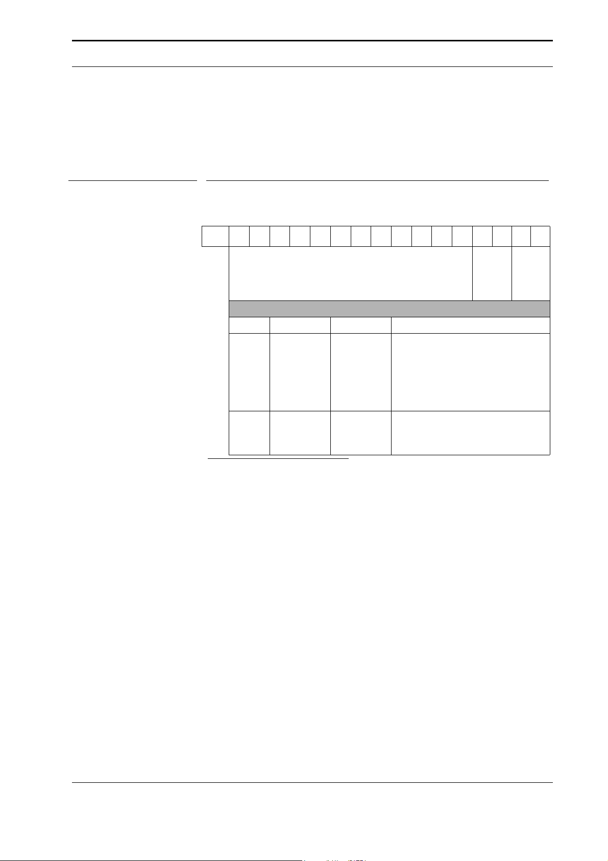
FIGURE 2. The slave address of the EEPROM:
2
C_CLK (GPIO26 of SA-1110) and I2C_DATA (GPIO27
Device Type
Identifier
1010000R/W
Read address: A1
•
• Write address: A0
MT6N (MT606) 5 von 49
High order
word address
Keith & Koep GmbH Functional specification
3.3 CompactFlash / PCMCIA
The MT6N is delivered with a Type I CompactFlash connector. In addition
(optional) there is a 68-leaded adaption connector which carries all signals for a single Type II PCMCIA-Slot connector.
TABLE 1. PCMCIA and CF Status Register
Offset 0x00000000 PCMCIA Status Register
15 14 13 12 11 10 9 8 7 6 5 4 3 2 1 0
Bit
Bits Name Type Description
1:0 BVD[2..1] Read Only
3:2 VS[2:1] Read Only
a. x means unconnected
Reserved
VS[1.0]
BVD[1:0]
Charge Condition of PC-card
00 - Battery low, data loss
01 - Warning, battery must be changed, but no data loss till now
10 - Battery low, data loss
11 - Battery OK
Voltage Sense lines
a
xx
- 5V operation
0x - 3V3 operation
3.3.1 PCMCIA
In the past memory expansion cards (specification 1.0) of the size of check cards
had just the purpose of providing memory. With the today generally valid specification 2.0 much of I/O units can be placed in a PCMCIA-slot. This includes for example SCSI-adaptation, Ethernet-Card or modem cards.
The PCMCIA-adaption connector on the board is designed on the basis of specification 2.0 (representative of this specification is the Personal Computer Memory
Card International Association)
The adjustment of the supply voltage and the programming voltage of the PCMCIA-card is to be effected by the Board Control Register.
3.3.2 CompactFlash
CompactFlash is a very small removable mass storage device. It provides complete
PCMCIA-ATA functionality and compatibility plus TrueIDE functionality compatible with ATA/ATAPI-4. At 43mm (1.7“) x 36mm (1.4“) x 3.3mm (0.13“), the
device’s thickness is less than one-half of a current PCMCIA Type II card. It is actually one-fourth the volume of a PCMCIA card. Compared to a 68-pin PCMCIA
card, a CompactFlash card has 50 pins (the connector is similar to the PCMCIA
card) but still conforms to PCMCIA-ATA specs. CompactFlash cards are designed
with flash technology, a non-volatile storage solution that does not require a battery
to retain data indefinitely. CompactFlash storage products are solid state, meaning
MT6N (MT606) 6 von 49

Keith & Koep GmbH Functional specification
they contain no moving parts, and provide users with much greater protection of
their data than conventional magnetic disk drives.
3.4 Board Control Register BCR
The MT6N board requires additional GPIO output functions, which are implemented in the Board Control Register (BCR) to control the Compact Flash, PCMCIA, display and something else.
TABLE 2. Board Control Register
Offset 0x02000000 Board Control Register
Bit
Reset
1514131211109876543210
????????00100000
Reserved
L_DISP
[3..0]
FORCE_ON
PCMCIA_RESET
PCMCIA_BUF_EN
CONTR_LOGIC
Bits Name Type Description
3:0
CONTR_
LOGIC
Write Only
PCMCIA Power Control Logic
see table 3 on page 8
[3..0]
Display enable
4 L_DISP Write Only
0 - Display off
1 - Display on
PCMCIA buffer enable
0 - PCMCIA buffer enable ON
1 - PCMCIA buffer enable OFF
Turn on RS232 tranceiver
0 - RS232 transceiver OFF
1 - RS232 transceiver ON
Resetting PCMCIA card
0 - Normal operation
1 - Resetting PCMCIA
5
6
7
PCMCIA_
BUF_EN
FORCE_
ON
PCMCIA_
RESET
Write Only
Write Only
Write Only
The PCMCIA-Switcher (MIC2562a-1) can be adjusted by the data lines D00 to
D03. The MIC2562a-1 switches between the three power supplies (0V, 3.3V and
MT6N (MT606) 7 von 49

Keith & Koep GmbH Functional specification
5.0V) and the programming voltages (OFF, 0V, 3.3V, 5.0V or 12.0V), which are
needed for the PCMCIA-cards.
TABLE 3. MIC2562a-1 Control Logic Table
D00 D01 D02 D03 Vcc out Vpp out
0000Clamped to Ground Clamped to Ground
0001Clamped to Ground High Z
0010Clamped to Ground High Z
0011Clamped to Ground High Z
01005V Clamped to Ground
01015V 5V
01105V 12V
01115V High Z
10003.3V Clamped to Ground
10013.3V 3.3V
10103.3V 12V
10113.3V High Z
1100Clamped to Ground Clamped to Ground
1101Clamped to Ground High Z
1110Clamped to Ground High Z
1111Clamped to Ground High Z
With setting the data bus D04 the display control signal L_DISP can be switched.
The important thing about that is the power on/off timing of the display. Usually the
correct sequence is as followed:
1. Power Supply
2. Input signal
3. Contrast voltage
4. Display control signal L_DISP
If you use another display as delivered from Keith & Koep you should test the correctness of the power on/off sequences.
Resetting the data bus D05 switches the address and control-signals of the PCMCIA-buffer.
With setting the data bus D06 the serial interface driver is switched on.
With setting the data bus D07 a reset-signal is sent to the PCMCIA-slot.
MT6N (MT606) 8 von 49

Keith & Koep GmbH Functional specification
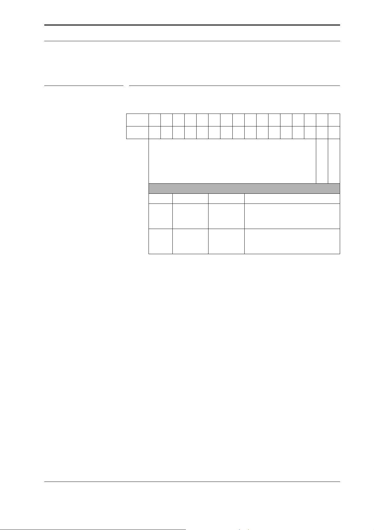
3.5 Real Time Clock (RTC)
MT6N contains a Low-Power RTC from Philips, called PCF8593. This chip uses
the same two wire bus as the serial EEPROM, which is described in figure 2 on
page 5.
FIGURE 3. The slave address of the RTC
Device Type
Identifier
1110000R/W
Read address: A3
Write address: A2
The RTC is either supplied from the onboard battery or from an external battery.
3.6 JTAG interfaces
The SA-1110 contains a JTAG port that allows test access to the I/O pins of the
device. The JTAG port is designed as a 10-pin header connector.
High order
word address
With a second JTAG interface program the CPLDs on board. It is designed as a 6pin header.
3.7 Reset
There are two sources of reset on the MT6N:
1. Power-on Reset
2. Reset from the watchdog timer
Power-on reset is generated automatically when power is applied to the board. It
can also be initiated by a push button switch attached to a 2-pole 0.1-inch pitch connector on the board.
Resets generated by any of these methods are equivalent and indistinguishable.
3.8 Power Supply
Power supply is possible on several ways:
First: The Power supply of MT6N is accessible by a power connector by Phoenix
with part number PSC 1,5/3-M. Pin 1 is the positive one (+24V) and Pin 3 is
Ground.
Second: It is also possible to supply MT6N by an optional PCB where the TTL I/O
ports are electrically isolated. More information: http://www.keith-koep.com.
Third: Supply through a 2-pin connector by Phoenix, which is optional and usually
not placed.
MT6N (MT606) 9 von 49

Keith & Koep GmbH Functional specification
3.9 Power generation on board
+12V are generated from the +24V power supply using a DC-DC converter. This
voltage is just needed for some PCMCIA cards and for some kinds of backlight
inverter of the display.
The power supplies +5V and +3V3 are generated from the +12V power by two further DC-DC converters. The +5V are used by PCMCIA or CompactFlash cards,
CAN and for backlight inverter. The +3V3 are used by Trizeps, Ethernet, PCMCIA
or CompactFlash cards, serial interfaces and something else.
3.10 GPIO
Both (Trizeps I and Trizeps II) modules put GPIOs at free disposal.
3.10.1 GPIO (Trizeps I)
The SA-1110 provides 28 general purpose I/O port pins for use in generating and
capturing application specific input and output signals. Each pin is programmable
as an input or output and as an interrupt source. Most GPIO pins have an alternate
function which can be invoked to enable additional functionality within the SA-
1110. If a GPIO is used for this alternate function it cannot be used as a GPIO at the
same time. The table below shows each GPIO pin with the using on MT6N and its
corresponding alternate function.
TABLE 4. GPIOs of SA1110 (Trizeps I) used on MT6 and their alternate functions
SA 1110
Pin
GP[27]
GP[26]
GP[25] ANGELBOOT in Start of angel BSL RTC Clock out
GP[24] PCD in PCMCIA card detect Reserved
GP[23] IRQ_IO
GP[22]
GP[21] IRQ_CAN
GP[21] MCP_CLK in
GP[20] INVALID_3
GP[19] IRQ_SMC
GP[18] DCD_3 in Data carrier detect (3) UART_SCLK1 in
GP[17] DSR_3 in Data set ready (3) SDLC_AAF out
GP[16] DTR_3 out Data terminal ready (3) SDLC_SCLK bi
GP[15] CTS_3 in Clear to send (3) UART_RXD in
GP[14] RTS_3 out Request to send (3) UART_TXD out
GP[13] CTS_1 in Clear to send (1) SPI_CS out
GP[12] RTS_1 out Request to send (1) SPI_CLK out
GP[11] SPI_RXD in in
GP[10] SPI_TXD out out
GP[2-9] LDD[8-15] out Display signal LDD[8-15] out
Function on
MT6 Dir Description
a
I2C_DATA
I2C_CLK
IRQ_CODEC
b
bi Data I2C-bus 32KHZ_OUT out
out Clock I2C-bus RCLK_OUT out
in Interrupt of TTL I/O TREQB in
c
in Interrupt of UCB1200 TREQA in
in Interrupt of CAN TIC_ACK out
in
RS232-Invalid-signal (3)
in Interrupt of Ethernet SSP_CLK in
Alternate
function Dir
d
UART_SCLK3 in
MT6N (MT606) 10 von 49

Keith & Koep GmbH Functional specification
TABLE 4. GPIOs of SA1110 (Trizeps I) used on MT6 and their alternate functions
SA 1110
Pin
Function on
MT6 Dir Description
Alternate
function Dir
GP[1] PRDY in Interrupt PCMCIA Reserved
GP[0] IRQ_PIC in Interrupt PIC Reserved
a. 100K pulled up
b. 100K pulled up
c. Used on Trizeps internally
d. The number in parenthesis named the serial port
3.10.2 GPIO (Trizeps II)
The PXA250 processor enables and controls its 81 general purpose I/O (GPIO) pins
through the use of 27 registers which configure the pin direction (input or output),
pin function, pin state (outputs only), pin level detection (inputs only), and selection
of alternate functions. The PXA250 processor provides 81 GPIO pins for use in
generating and capturing application specific input and output signals. Each pin can
be programmed as either an input or output.When programmed to be an input, a
GPIO can also serve as an interrupt source. If a GPIO is used for it alternate function it cannot be used as a GPIO at the same time. The table below shows each
GPIO pin with the using on MT6N and its corresponding alternate function.
TABLE 5. GPIOs of PXA250 (Trizeps II) used on MT6 and their alternate functions
PXA250
Pin
GP[80] CS[4] out Active low chip select 4 nCS[4] out
GP[79] CS[3]
GP[78] CS[2]
GP[77] L_BIAS out LCD AC BIAS LCD_ACBIAS out
GP[76] L_PCLK out LCD pixel clock LCD_PCLK out
GP[75] L_LCLK out LCD line clock LCD_LCLK out
GP[74] L_FCLK out LCD frame clock LCD_FCLK out
GP[73] LDD15 out LCD data pin 15 LDD[15] out
GP[73] Memory controller grant MBGNT out
GP[72] LDD14 out LCD data pin 14 LDD[14] out
GP[72] 32 KHz clock 32 kHz out
GP[71] LDD13 out LCD data pin 13 LDD[13] out
GP[71] 3.6 MHz oscillator clock 3.6 MHz out
GP[70] LDD12 out LCD data pin 12 LDD[12] out
GP[70] Real Time Clock (1Hz) RTCCLK out
GP[69] LDD11 out LCD data pin 11 LDD[11] out
GP[69] MMC_CLK MMCCLK out
GP[68] LDD10 out LCD data pin 10 LDD[10] out
GP[68] MMC Chip Select 1 MMCCS1 out
Function on
MT6 Dir Description
out Active low chip select 3 nCS[3] out
out Active low chip select 2 nCS[2] out
Alternate
function
Di
r
MT6N (MT606) 11 von 49

Keith & Koep GmbH Functional specification
TABLE 5. GPIOs of PXA250 (Trizeps II) used on MT6 and their alternate functions
PXA250
Pin
Function on
MT6 Dir Description
Alternate
function
Di
r
GP[67] LDD09 out LCD data pin 9 LDD[9] out
GP[67] MMC Chip Select 0 MMCCS0 out
GP[66] LDD08 out LCD data pin 8 LDD[8] out
GP[66] MBREQ MBREQ in
GP[58]-
LDD[00-07] out LCD data pin 0 to7 LDD[0-7] out
GP[65]
GP[57] PIOIS16
GP[56] PWAIT
GP[55] PREG
in Bus Width select I/O card nIOIS16 in
in Wait signal for card space nPWAIT in
out Card address bit 26 nPREG out
GP[54] PSKTSEL out Socket select for card space PSKTSEL out
GP[54] MMC Clock MMCCLK out
GP[53] PCE2
out Card Enable for card space nPCE[2] out
GP[53] MMC Clock MMCCLK out
GP[52] PCE1
GP[51] PIOW
GP[50] PIOR
GP[49] PWE
GP[48] POE
out Card Enable for card space nPCE[1] out
out I/O Write for Card space nPIOW out
out I/O Read for Card space nPIOR out
out Write enable for card space nPWE out
out Output Enable for card space nPOE out
GP[47] TXD_2 out STD_UART transmit data TXD out
GP[47] ICP transmit data ICP_TXD out
GP[46] RXD_2 in STD_UART receive data RXD in
GP[46] ICP receive data ICP_RXD in
GP[45] BT_RTS out BTUART request to send RTS out
GP[44] BT_CTS in BTUART clear to send CTS in
GP[43] BT_TXD out BTUART transmit data BTTXD out
GP[42] BT_RXD in BTUART receive data BTRXD in
GP[41] FF_RTS out FFUART request to send RTS out
GP[40] FF_DTR out FFUART data terminal ready DTR out
GP[39] FF_TXD out FFUART transmit data FFTXD out
GP[39] MMC Chip select 1 MMCCS1 out
GP[38] FF_RI in FFUART ring indicator RI in
GP[37] FF_DSR in FFUART data set ready DSR in
GP[36] FF_DCD in FFUART data carrier detect DCD in
GP[35] FF_CTS in FFUART clear to send CTS in
GP[34] FF_RXD in FFUART receive data FFRXD in
GP[34] MMC chip select 0 MMCCS0 out
GP[33] CS5
out Active low chip select 5 nCS[5] out
GP[32] AC97 Sdata_in1 SDATA_IN1 in
a
GP[31]
AC97SYNC
out AC97 sync SYNC out
MT6N (MT606) 12 von 49

Keith & Koep GmbH Functional specification
TABLE 5. GPIOs of PXA250 (Trizeps II) used on MT6 and their alternate functions
PXA250
Pin
Function on
MT6 Dir Description
Alternate
function
Di
r
GP[31] I2S sync SYNC out
a
GP[30]
AC97DOUT
out AC97 Sdata_out SDATA_OUT out
GP[30] I2S Sdata_out SDATA_OUT out
GP[29]
AC97DIN
a
in AC97 Sdata_in0 SDATA_IN0 in
GP[29] I2S Sdata_in SDATA_IN in
GP[28]
BITCLK
a
in AC97 bit_clk BITCLK in
GP[28] I2S bit_clk BITCLK in
GP[28] I2S bit_clk BITCLK out
GP[27] EXT_CLK in
GP[26] RXD in
GP[25] PWR_FAIL in Powerfail IRQ TXD out
GP[24] PCD
GP[23] IRQ_IO
in PCMCIA card detect SFRM out
in TTL I/O IRQ SCLK out
GP[22]
GP[21] IRQ_CAN
GP[20] INVALID_3
GP[19] IRQ_SMC
in CAN IRQ
in RS232 Invalid signal DREQ[0] in
in Ethernet IRQ DREQ[1] in
GP[18] RDY in External bus ready RDY in
GP[17] PWM1 output PWM1 out
GP[16] PWM0 output PWM0 out
GP[15] CS1
out Active low chip select 1 nCS[1] out
GP[14] Memory bus master request MBREQ in
GP[13] Memory controller grant MBGNT out
GP[12] 32 kHz out 32 kHz out
GP[11] 3.6 MHz oscillator out 3.6 MHz out
GP[10] Real time clock (1Hz) RTCCLK out
GP[9] MMC Chip select 1 MMCCS1 out
GP[8] MMC Chip select 0 MMCCS0 out
GP[7] 48 MHz clock output 48 MHz clock out
GP[6] MMC clock MMCCLK out
GP[5]
GP[4]
GP[3]
a
GP[2]
IRQ_CODEC
in UCB1x00 IRQ
GP[1] PRDY in PCMCIA IRQ GP_RST in
GP[0] IRQ_PIC in PIC IRQ
a. used on Trizeps II internally
MT6N (MT606) 13 von 49

Keith & Koep GmbH Functional specification
3.11 Ethernet
The Ethernet Controller (LAN91C96 by SMSC) on the MT6N board supports the
IEEE 802.3 (ANSI 8802-3) Ethernet Standards. It is connected to a 10 Base-T filter
module. The Ethernet connector is of the type RJ45. The controller in the configuration of MT6N provides:
• 6K Bytes of On-Chip RAM
• Support of enhanced transmit queue management
• Direct interface to ISA buses with no wait states
• Fast access time (40ns)
• Pipelined data path
• Integrated 10Base-T Transceiver functions:
•Driver and receiver
•Link integrity test
•Receive polarity detection and correction
• 10 Mb/s Manchester Encoding / Decoding and clock recovery
• Automatic retransmission, bad packet rejection and transmit padding
• Optional configuration via serial EEPROM interface (jumperless)
• Two direct driven LEDs for diagnostics (transmit / receive indication)
3.12 Serial ports
The MT6 provides four kinds of serial ports:
• USB
• UART
• IrDA
• SPI
3.12.1 Serial port 0 - USB Device Controller
Serial port 0 is an universal serial bus device controller (UDC) that supports three
endpoints and can operate half-duplex at a baud rate of 12 Mbps (slave only, not a
host or hub controller).The UDC is USB-compliant and supports all standard device
requests is issued by the host. The external pins dedicated to this interface are
UDC+ and UDC-. The USB protocol uses differential signalling between the two
pins for half-duplex data transmission. A 1.5 KOhm pull-up resistor is connected to
the USB cable’s D+ signal to pull the UDC+ pin high when not driven. This signifies the UDC is a high-speed, 12 Mbps device and provides the correct polarity for
data transmission.
Serial port 0 is accessible by an SL1-4 (four pin header). However, the user should
refer to the Universal Serial Bus Specification, Revision 1.0
of the USB protocol and its operation.
3.12.2 Serial port 1 - UART
Serial port 1 is configured as an universal asynchronous receiver / transmitter
(UART) serial controller. A Maxim MAX3223 RS232 transceiver is used to manage the level conversion and line interface. The device has a power saving auto-
1
for a full description
1. The latest revision of the Universal Serial Bus Specification Revision 1.0 can be accessed
via the World Wide Web Internet side at: http://www.teleport.com/~usb/
MT6N (MT606) 14 von 49

Keith & Koep GmbH Functional specification
matic shutdown that powers down the chip if no valid RS232 levels are detected.
The component may also be forced off by the FORCEON signal. Serial port 1 is
accessible by the female serial port connector J18 (10-pin header). The external pins
dedicated to this interface are TXD1 and RXD1. Further GPIO 12 and 13 are used
as hand-shake signals RTS and CTS.
For the communication between the PC (DB9 male) and the MT6 a serial extension
cable is needed. Therefore the serial port J18 (10 pin header) is to be connected with
a short flat cable to a DB9 female connector (see figure 7 on page 36).
3.12.3 Serial port 2 - Infrared communications port
The infrared communications port (ICP) operates at half-duplex and provides direct
connection to commercially available Infrared Data Association (IrDA) compliant
LED transceivers. The ICP supports both the original IrDA standard with speeds up
to 115.2 Kbps as well as the newer 4-Mbps standard. Both standards use different
bit encoding techniques and serial packet formats. Low-speed IrDA transmission
uses the Hewlett-Packard Serial Infrared standard (HP-SIR) for bit encoding and an
UART as the serial engine; high-speed uses Four-Position Pulse Modulation
(4PPM) and a specialized serial packet protocol developed expressly for IrDA
transmission. Serial port 2 is accessible by a 10-pin header. The external pins dedicated to the ICP are TXD2 and RXD2.
FIGURE 4. Sample: Use of IrDA
MT6N (MT606) 15 von 49
Keith & Koep GmbH Functional specification
TABLE 6. IrDA Control Register
Offset 0x02400000 IrDA Control Register
1514131211109876543210
Bit
Reset
??????????????01
Bits Name Type Description
0 IRDA_SD Write Only
1
Alternately you can use serial port 2 as an UART.
3.12.4 Serial port 3 - UART
Serial port 3 is configured as an universal asynchronous receiver / transmitter
(UART) serial controller. A Maxim MAX3243 RS232 transceiver is used to
manage the level conversion and line interface. The device has a power saving automatic shutdown that powers down the chip if no valid RS232 levels are detected.
The component may also be forced off by the FORCEON signal. Serial port 3 is
accessible by the male serial port connector J12 (DSUB9M). This port provides
RTS, CTS, DSR, DTR and DCD modem signals to support a serial IO port PC synchronous application.
IRDA_
MODE
Reserved
Write Only
IRDA_SD
IRDA_MODE
IrDA Shutdown
0 - IrDA activ
1 - IrDA inactiv
IrDA Mode
0 - Low speed
1 - High speed
3.12.5 Serial port 4 - SSP
The synchronous serial port (SSP) of the SA-1110 is used to interface to a variety of
analog-to-digital converters, audio and telecom codecs, memory chips, and keypad
controllers as well as other miscellaneous serial devices. The SSP supports the
National Microwire and Texas Instruments synchronous serial protocols as well as a
subset of the Motorola serial peripheral interface (SPI) protocol. Serial port 4 controls full-duplex synchronous serial transfer between the SA-1110 and off-chip
devices. The SSP functions as a master only and communicates to the off-chip slave
device by driving a serial bit rate clock ranging from 7.2 KHz to 1.8432 MHz along
with a frame synchronisation pulse to denote the start of each frame transfer, and
supports any data format between 4 and 16 bits. The external pins dedicated to this
interface are GPIO 10 to 13.
MT6N (MT606) 16 von 49

Keith & Koep GmbH Functional specification
3.13 CAN interface
The CAN (Controller Area Network) is a serial bus system especially suited for networking “intelligent“ devices as well as sensors and actuators within a system or
subsystem. MT6 uses the SJA1000, a stand-alone CAN controller made by Philips.
It is used within automotive and general industrial environments. SJA1000 is the
successor of the PCA82C200 CAN controller (BasicCAN) from Philips Semiconductors. Additionally, a new mode of operation is implemented (PeliCAN) which
supports the CAN 2.0B protocol specification with several new features.
This controller offers the following features:
• PIN and Electrical compatibility to the PCA82C200 stand-alone CAN controller
• PCA82C200 mode (BasicCan mode is default)
• Extended receive buffer (64-byte FIFO)
• CAN 2.0B protocol compatibility
• Supports 11-bit identifier as well as 29-bit identifier
• Bit rates up to 1Mbits/s
• PeliCAN mode extensions:
•Error counters with read/write access
•Programmable error warning limit
•Last error code register
•Error interrupt for each CAN-bus error
•Arbitration lost interrupt with detailed bit position
•Single-shot transmission (no re-transmission)
•Listen only mode (no acknowledge, no active error flags)
•Hot plugging support (software driven bit rate detection)
•Acceptance filter extension (4-byte code, 4-byte mask)
•Reception of ’own’ messages (self reception request)
To use the can interface, please refer to the pinout description of the can connector
(J3 DB9 female) in table 12 on page 25.
3.14 TTL I/O
MT6 offers 16 TTL Inputs and 16 TTL Outputs. There are 2 I/O connectors called
J15 and J16 on the board. Both connectors comprise each 8 TTL Input ports and 8
TTL Output ports. The pinout is shown in table 24 on page 33 and table 25 on
page 34. The output signals (OUTPUT[00:15]) correspond with dataline signals
D[00:15], which are switched by a CPLD. They will be selected by addressing
0x19800000 (\CS_IO_OUT and \CS_IO_IN). The Inputs can be read as follows:
read = *(short *) ADR
The Outputs can be written as follows:
*(short *) portadr = value
Keith & Koep GmbH offers an optional circuit board with electrically isolated
ports, one which can be placed directly on J15 and another one that will be connected by a flat cable to J16. With this board it is possible to provide +24V for the
MT6N (MT606) 17 von 49

Keith & Koep GmbH Functional specification
MT6. You’ll find more information about the I/O board on our homepage
(www.keith-koep.com/trizeps.html)
3.15 Audio In/Out
The Trizeps board includes a single chip integrated mixed signal audio and telecom
codec (Philips UCB 1200). JJ2 and JJ3 on the MT6 give access to the speaker and
microphone signals. The pinout of JJ2 is shown in table 34 on page 39 and of JJ3 in
table 35 on page 39.
From MT6 Version 5 the board can be fitted out with an audio stereo connector.
3.16 Display connector and 4 wire Touch Panel
The SA-1110 on the Trizeps offers a 16 bit LCD-controller. The audio and telecom
codec (see chapter 3.15, "Audio In/Out" on page 18) provides also a 4 wire touch
screen interface. The relevant signals are accessible at J14 see table 23 on page 32.
The contrast voltage can be adjusted by an Digitally-Controlled Potentiometer by
Xicor. The device consists of a resistor array, wiper switches, a control section, and
nonvolatile memory. The wiper position is controlled by a three-wire interface.
The potentiometer is implemented by a resistor array composed of 99 resistive elements and a wiper switching network. Between each element and at either end are
tap points accessible to the wiper terminal. The position of the wiper element is controlled by the CS, U/D, and INC inputs. The position of the wiper can be stored in
nonvolatile memory and then be recalled upon a subsequent power-up operation.
TABLE 7. Display Contrast Register
Offset 0x03800000 Display Contrast Register
1514131211109876543210
Bit
Reset
??????????????11
Bits Name Type Description
0
1
2
EEPOT_
EEPOT_
EEPOT_
CS
INC
U_D
Reserved
Write Only
Write Only
Write Only
EEPOT_U_D
Chip Select of EEPOT
0 - activ
1 - inactiv
Increment of EEPOT
0 - increment by 1
1 - inactive
Direction (Up/Down)of EEPOT
0 - decrement
1 - increment
EEPOT_CS
EEPOT_INC
3.17 MultiMediaCard
The MultiMediaCard standard grew out of a joint development between SanDisk
Corporation and Siemens AG/Infineon Technologies AG, and was introduced in
MT6N (MT606) 18 von 49

Keith & Koep GmbH Functional specification
November 1997. MultiMediaCards weigh less than two grams and, about the size of
a postage stamp, are the world’s smallest (24mm x 32mm x 1.4 mm) removable
solid-state memory solutions for mobile applications. These convenient, reliable,
rugged and lightweight standardized data carriers store up to 64 MBytes.
MultiMediaCards use ROM technology for read-only applications and Flash technology for read/write applications. The cards are fast for excellent system performance; energy efficient for prolonged battery life in portable products; and costefficient for use in systems sold at consumer price points. The simple molded package has a seven pad (pin) serial interface. This easy-to-install simple serial interface
offers easy integration into various devices regardless of the microprocessor used.
The MultiMediaCard has a wide variety of uses in some of the most exciting products on the market today.
3.18 PS/2 connector
The MT6 is fitted out with an PS/2 connector which allows the use of a keyboard or
a mouse.
3.19 Powerfail - Interrupt
Falling down power supply under ~14V generates an interrupt GPIO25 (PowerfailIRQ).
3.20 Uninterruptible Power Supply (UPS)
The easiest way to get an UPS is to use the following electrical circuit.
FIGURE 5. UPS
+12V
GND
+++++
RRRRR
C
Values:
R: 22K
RV: 10
C: 10F / 2,3V (UltraCap by EPCOS)
D: 1N5819
CCCC
D
R
V
Ω
(Power resistor)
Ω
D
You can use connector J23 to supply this circuit with +12V and Ground.
This circuit is able to supply the MT6 with Trizeps in case of Powerfail for 15 seconds.
MT6N (MT606) 19 von 49

Keith & Koep GmbH Functional specification
TABLE 8. UPS Register
Offset 0x02800000 UPS Register
Bit
Reset
1514131211109876543210
???????????01100
Reserved
CHARGE
BATT_EMPTY
AUTO_PWR_OFF
AUTO_DSPL_OFF
BATT_EN
Bits Name Type Description
External battery enable signal
0 - external battery OFF
1 - external battery ON
Charge external battery
0 - Do not charge
1 - Charge
0 BATT_EN
1 CHARGE
Output
R/W
Output
R/W
Turn off system flag
0 - OS does not power down after
powerfail-IRQ
1 - OS powers down after power-
2
AUTO_
PWR_OFF
Flag
R/W
fail-IRQ
AUTO_
3
DISPL_
OFF
4
BATT_
EMPTY
Flag
R/W
Input
Read Only
Turn off backlight inverter flag
0 - Leave backlight ON
1 - Powerfail-IRQ handler switches backlight OFF
External battery status
0 - External battery empty
1 - External battery full
MT6N (MT606) 20 von 49

Keith & Koep GmbH Functional specification
Appendix A
In this chapter you can find detailed description about all headers and connectors on
MT6.
MT6N (MT606) 21 von 49

Keith & Koep GmbH Functional specification
A.1 Overview of all jumpers, connectors
TABLE 9. Overview of all jumpers and connectors
Name Function Type
J1 Power Supply
J2 CompactFlash connector 3M N7E50-7516VY-2O
J3 CAN connector DSUB9 female
J4 JTAG connector (CPLD) Header SL2-6
J5 RS232 connector (port 3) DSUB9 male
J6 Ethernet connector RJ45
J7 JTAG connector (Trizeps) Header SL2-10
J8 BLI (external) Header SL3-4 (optional)
J9 BLI (direct) Header SL3-4 (optional)
J10 Power Supply
J11 PCMCIA interface 2 x Header SL2-34 (optional)
J12 Serial port 3 (Transformed signals) Header SL2-10 (optional)
J13 Serial port 3 (TTL-signals) Header SL2-10 (optional)
J14 Display connector Header SL2-40
J15 TTL I/O connector Header SL2-26
J16 TTL I/O connector Header SL2-26
J17 Serial port 2 connector Header SL2-10
J18 RS232 connector (port 1) Header SL2-10
J19 SPI and A/D connector Header SL2-14
J20 USB / IrDA connector Header SL2-10
J21 PIC16F84 program connector Header SL1-6
J22 PS/2 connector Molex 87123-08
J23 Uninterruptible Power Supply
(UPS) connector
J24 MultiMediaCard (MMC) connector JST Drawing No. KRD-24511-1 (optional)
JJ1 CAN Termination Header SL1-2
JJ2 Speaker connector Header SL1-2
JJ3 Microphone connector Header SL1-2
JJ5 Reset connector Header SL1-2
JJ6 Battery (onboard or external) Header SL1-4
JJ7 Invalid signal for serial connection Header SL1-3
JJ8 Angelboot Header SL1-2
S1 Audio stereo connector Reichelt EBS35A
U1 Trizeps SODIMM 144
X9 Display LM8V31 MOLEX 53261-1590 (optional)
X10 Display LM8V31 MOLEX 53261-1490 (optional)
X14 Touch LM8V31 JST 04FE-ST-VK-N (optional)
Phoenix
(optional)
Phoenix
Header SL2-10
MSTBVA 2,5/2-G-5,08
PSC 1,5/3-M
MT6N (MT606) 22 von 49

Keith & Koep GmbH Functional specification
FIGURE 6. Jumper and connector locations
MT6N (MT606) 23 von 49
Keith & Koep GmbH Functional specification
A.2 Power Supply (I)
The Power Supply connector is produced by PHOENIX. It’s a 2 pin connector with
the part number MSTBVA 2,5/2-G-5,08. This part is optional and usually not
placed.
TABLE 10. J1 - Power Supply
Pin Signal Description
1 24V Power Supply
2 GND Ground
A.3 CompactFlash connector
In table 11 on page 24 you see the pin description of the CompactFlash Connector.
The „MC_“ in front of the signal names is used by buffered signals. For example:
MC_D01 means the second databus of SA1110 buffered by CPLD.
TABLE 11. J2 - CompactFlash Connector
Pin Signal Description
1 GND Ground
2 MC_D03 Databus
3 MC_D04 Databus
4 MC_D05 Databus
5 MC_D06 Databus
6 MC_D07 Databus
7MC_CE1
8 MC_A10 Memory address bus
9 MC_OE Output Enable signal
10 MC_A09 Memory address bus
11 MC_A08 Memory address bus
12 MC_A07 Memory address bus
13 MC_VDD Power Supply
14 MC_A06 Memory address bus
15 MC_A05 Memory address bus
16 MC_A04 Memory address bus
17 MC_A03 Memory address bus
18 MC_A02 Memory address bus
19 MC_A01 Memory address bus
20 MC_A00 Memory address bus
21 MC_D00 Databus
22 MC_D01 Databus
23 MC_D02 Databus
24 MC_IOIS
Card Enable signal
Write Protect signal
MT6N (MT606) 24 von 49

Keith & Koep GmbH Functional specification
TABLE 11. J2 - CompactFlash Connector
Pin Signal Description
25 MC_CD2 Card Detect signal
26 MC_CD1
27 MC_D11 Databus
28 MC_D12 Databus
29 MC_D13 Databus
30 MC_D14 Databus
31 MC_D15 Databus
32 MC_CE2
33 MC_VS1
34 MC_IOR
35 MC_IOW
36 MC_WE
37 MC_RDY
38 MC_VDD Power Supply
39 nc not connected
40 MC_VS2
41 PCM_RESET Reset signal
42 MC_WAIT
43 nc not connected
44 MC_REG
45 MC_BVD2 Battery Voltage Detect signal
46 MC_BVD1 Battery Voltage Detect signal
47 MC_D08 Databus
48 MC_D09 Databus
49 MC_D10 Databus
50 GND Ground
Card Detect signal
Card Enable signal
Voltage Sense signal
I/O Read signal
I/O Write signal
Write Enable signal
Ready / Busy signal
Voltage Sense signal
Wait signal
Attribute-Memory-Select or Register signal
A.4 CAN connector
The CAN-interface is electrically isolated. Usually the CAN-interface is terminated
with an 120 Ohm resistor by closing jumper JJ1.
The CAN connector is a 9-pin female DSUB connector with the following pinout:
TABLE 12. J3 - CAN connector
Pin Signal Description
1 nc not connected
2 CANL negative differential signal
3 CAN_GND Ground CAN
MT6N (MT606) 25 von 49

Keith & Koep GmbH Functional specification
TABLE 12. J3 - CAN connector
Pin Signal Description
4 nc not connected
5 nc not connected
6 nc not connected
7 CANH positive differential signal
8 nc not connected
9 CAN_VCC Power Supply CAN
A.5 JTAG connector (CPLD)
On the MT6 there are two CPLD by Xilinx which can be programmed through an 6pin header with the following pinout.
TABLE 13. J4 - JTAG connector (CPLD)
Pin Signal Description
1 +3V3 Power Supply
2 GND Ground
3 XC_TCK Clock signal
4 XC_TDO2 Output signal
5 XC_TDI Input signal
6 XC_TMS Mode signal
A.6 RS232 connector (port 3)
The connector J5 is a male DB9 connector with the following pin description.
TABLE 14. J5 - Serial Interface connector (port 3)
Pin Signal Description
1 DCD3_V24X Data Carrier Detect
2 RXD3_V24X Receive Data
3 TXD3_V24X Transmit Data
4 DTR3_V24X Data Terminal Ready
5 GND Ground
6 DSR_V24X Data Set Ready
7 RTS3_V24X Request to Send
8 CTS3_V24X Clear to Send
9 +5V Power Supply
MT6N (MT606) 26 von 49

Keith & Koep GmbH Functional specification
A.7 Ethernet connector
The Ethernet connector is an usually RJ45 connector with the following pin
description.
TABLE 15. J6 - Ethernet connector
Pin Signal Description
1 TPETXP Transmit differential output
2 TPETXN Transmit differential output
3 TPERXP Receive differential output
4 nc not connected
5 nc not connected
6 TPERXN Receive differential output
7 nc not connected
8 nc not connected
A.8 JTAG connector (Trizeps)
The JTAG connector to program Flash memory on Trizeps is a 2 row 10 pin header.
The pinout is shown in table 16 on page 27
TABLE 16. J7 - JTAG connector (Trizeps)
Pin Signal Description
1TRSTTest interface reset
2 +3V3 Power Supply
3 TDI JTAG test interface data input
4 +3V3 Power Supply
5 TDO JTAG test interface data output
6 GND Ground
7 TMS JTAG test interface mode select
8 GND Ground
9 TCK JTAG test interface reference clock
10 GND Ground
MT6N (MT606) 27 von 49

Keith & Koep GmbH Functional specification
A.9 Backlight Inverter (BLI) (external)
For backlight power you can either use the onboard BLI or an external BLI. The
external one can be connected by an 4-pin header with the following pinout: This
part is optional and usually not placed.
TABLE 17. J8 - Backlight Inverter connector (external)
Pin Signal Description
1 BL_POWER Default Value: +5V (switchable to +12V)
2 GND Ground
3 nc not connected
4 nc not connected
A.10 Backlight Inverter (BLI) (direct)
The backlight power on the MT6 can be build by a Backlight inverter from TDK
with the part name CXA-M10A-L. The pinout of the connector (Header SL3-4) is
shown in table 18 on page 28.This part is optional and usually not placed.
TABLE 18. J9 - Backlight Inverter connector
Pin Signal Description
1 OUT1 Power out
2 nc not connected
3 nc not connected
4 OUT_GND Power Ground
A.11 Power Supply (II)
The Power supply of MT6 can happen on many ways. Usually the power connector
J10 by Phoenix with the part number PSC 1,5/3-M is used.
TABLE 19. J10 - Power connector
Pin Signal Description
1 +24V Power supply (in range of +15V to +24V)
2 nc not connected
3 GND Ground
A.12 PCMCIA interface
Normally the MT6 is delivered with a CompactFlash connector. Alternately the
board can fitted out with an header (4 rows of 17 pins) for an PCMCIA-adapter
board. It is available by Keith & Koep. In table 20 on page 29 the signals are
MT6N (MT606) 28 von 49

Keith & Koep GmbH Functional specification
described in consideration of using only memory cards or using memory and I/O
cards.This part is optional and usually not placed.
TABLE 20. PCMCIA-slot J4
Pin Signal Description
1 GND Ground
2 D03 Databus
3 D04 Databus
4 D05 Databus
5 D06 Databus
6 D07 Databus
7CE1
8 A10 Memory address bus
9OE
10 A11 Memory address bus
11 A09 Memory address bus
12 A08 Memory address bus
13 A13 Memory address bus
14 A14 Memory address bus
15 WE
16 IREQ
17 Vcc Power Supply
18 Vpp1 Program Voltage
19 A16 Memory address bus
20 A15 Memory address bus
21 A12 Memory address bus
22 A07 Memory address bus
23 A06 Memory address bus
24 A05 Memory address bus
25 A04 Memory address bus
26 A03 Memory address bus
27 A02 Memory address bus
28 A01 Memory address bus
29 A00 Memory address bus
30 D00 Databus
31 D01 Databus
32 D02 Databus
33 IOIS16
34 GND Ground
35 GND Ground
36 CD1
/PGM Write-enable signal / Program signal
Card Enable signal
Output enable signal
Ready / Busy signal
Interrupt request signal
Write-Protect signal
Card-Detect signal
MT6N (MT606) 29 von 49

Keith & Koep GmbH Functional specification
TABLE 20. PCMCIA-slot J4
Pin Signal Description
37 D11 Databus
38 D12 Databus
39 D13 Databus
40 D14 Databus
41 D15 Databus
42 CE2
43 VS1
44 IORD
45 IOWR
46 A17 Memory address bus
47 A18 Memory address bus
48 A19 Memory address bus
49 A20 Memory address bus
50 A21 Memory address bus
51 Vcc Power Supply
52 Vpp2 Program Voltage
53 A22 Memory address bus
54 A23 Memory address bus
55 A24 Memory address bus
56 A25 Memory address bus, grounded
57 VS2
58 RESET Reset signal
59 WAIT
60 INPACK
61 REG
62 SPKR
63 STSCHG
64 D08 Databus
65 D09 Databus
66 D10 Databus
67 CD2
68 GND Ground
Card-Enable signal
Voltage sense
reserved
I/O-Read signal
reserved
I/O-Write signal
Voltage sense
Wait signal
reserved
Input Acknowledge signal
Attribute-Memory-Select- or Register-Signal
Battery Voltage Detect signal
Speaker- or Digital-Audio connect
Battery Voltage Detect
Status-Changed signal
Card-Detect signal
MT6N (MT606) 30 von 49

Keith & Koep GmbH Functional specification
A.13 Serial port 3 connectors for other serial interface than RS232
If you want to use another serial interface than RS232 you can use two 10-pin headers. At one of them, connector J13 (table 22 on page 31), serial port 3 TTL-signals
are available and at the other one, connector J12 (table 21 on page 31), the transformed signals are available.Both connectors are optional and usually not placed.
TABLE 21. J12 - Serial port 3 (transformed signals)
Pin Signal Description
1 DCD3_V24X Data Carrier Detect
2 DSR3_V24X Data Set Ready
3 RXD3_V24X Receive Data
4 RTS3_V24X Request To Send
5 TXD3_V24X Transmit Data
6 CTS3_V24X Clear To Send
7 DTR3_V24X Data Terminal Ready
8 +5V Power Supply
9 GND Ground
10 nc not connected
TABLE 22. J13 - Serial port 3 (TTL-signals)
Pin Signal Description
1 +3V3 Power Supply
2+5V Power Supply
3 TXD_3 Transmit Data
4 RXD_3 Receive Data
5DCD_3 Data Carrier Detect
6 DTR_3 Data Terminal Ready
7 DSR_3 Data Set Ready
8 RTS_3 Request To Send
9 CTS_3 Clear To Send
10 GND Ground
MT6N (MT606) 31 von 49

Keith & Koep GmbH Functional specification
A.14 Display connector
You can connect an Sharp DSTN display called LM8V31 directly to the MT6N. If
you want to use another display you have to use the 40-pin header, where are all rel-
evant signals available. table 23 on page 32 describes the pins and their functions.
TABLE 23. J14 - Display connector (40-pin Header)
Pin Signal Description
1 LDD00 LCD controller display data (Trizeps - SA-1110)
2 LDD01 LCD controller display data (Trizeps - SA-1110)
3 LDD02 LCD controller display data (Trizeps - SA-1110)
4 LDD03 LCD controller display data (Trizeps - SA-1110)
5 LDD04 LCD controller display data (Trizeps - SA-1110)
6 LDD05 LCD controller display data (Trizeps - SA-1110)
7 LDD06 LCD controller display data (Trizeps - SA-1110)
8 LDD07 LCD controller display data (Trizeps - SA-1110)
9 LDD08 LCD controller display data (Trizeps - SA-1110)
10 LDD09 LCD controller display data (Trizeps - SA-1110)
11 LDD10 LCD controller display data (Trizeps - SA-1110)
12 LDD11 LCD controller display data (Trizeps - SA-1110)
13 LDD12 LCD controller display data (Trizeps - SA-1110)
14 LDD13 LCD controller display data (Trizeps - SA-1110)
15 LDD14 LCD controller display data (Trizeps - SA-1110)
16 LDD15 LCD controller display data (Trizeps - SA-1110)
17 L_FCLK LCD frame clock (Trizeps - SA-1110)
18 L_LCLK LCD line clock (Trizeps - SA-1110)
19 L_PCLK LCD pixel clock (Trizeps - SA-1110)
20 L_BIAS LCD ac bias drive (Trizeps - SA-1110)
21 TSMX negative X-plate touch screen (Trizeps - UCB 1200)
22 TSMY negative Y-plate touch screen (Trizeps - UCB 1200)
23 TSPX positive X-plate touch screen (Trizeps - UCB 1200)
24 TSPY positive Y-plate touch screen (Trizeps - UCB 1200)
25 L_DISP LCD on
26 NC not connected
27 +3V3 Power supply
28 GND Ground
29 +5V Power supply
30 GND Ground
31 +12V Power supply
32 GND Ground
33 GND Ground
34 GND Ground
35 I2C_DATA
Data I
2
C Bus (Trizeps - SA-1110/GP27)
MT6N (MT606) 32 von 49

Keith & Koep GmbH Functional specification
TABLE 23. J14 - Display connector (40-pin Header)
Pin Signal Description
36 I2C_CLK
Clock I
37 IRQ_PIC Interrupt of the PIC (optional)
38 NC not connected
39 NC not connected
40 BL_POWER Backlight power
A.15 TTL I/O connector
The connectors for the 16 TTL I/Os are called J15 and J16. The pinout of J15 is
shown in table 24 on page 33, the other one in table 25 on page 34.
2
C Bus (Trizeps - SA-1110/GP26)
TABLE 24. J15 - TTL I/O Connector (Databus 00 to 07)
Pin Signal Description
1 GND Ground
2 OUTPUT00 TTL Output
3 OUTPUT01 TTL Output
4 OUTPUT02 TTL Output
5 OUTPUT03 TTL Output
6 OUTPUT04 TTL Output
7 OUTPUT05 TTL Output
8 OUTPUT06 TTL Output
9 OUTPUT07 TTL Output
10 GND Ground
11 INPUT00 TTL Input
12 INPUT01 TTL Input
13 INPUT02 TTL Input
14 INPUT03 TTL Input
15 INPUT04 TTL Input
16 INPUT05 TTL Input
17 INPUT06 TTL Input
18 INPUT07 TTL Input
19 +3V3 Power Supply
20 +3V3 Power Supply
21 IRQ_IO Interrupt Request TTL I/O
22 EXT_GND Power Supply (external)
23 EXT_GND Power Supply (external)
24 EXT_GND Power Supply (external)
MT6N (MT606) 33 von 49

Keith & Koep GmbH Functional specification
TABLE 24. J15 - TTL I/O Connector (Databus 00 to 07)
Pin Signal Description
25 EXT_24V Power Supply (external)
26 EXT_24V Power Supply (external)
TABLE 25. J16 - TTL I/O Connector (Databus 08 to 15)
Pin Signal Description
1 GND Ground
2 OUTPUT08 TTL Output
3 OUTPUT09 TTL Output
4 OUTPUT10 TTL Output
5 OUTPUT11 TTL Output
6 OUTPUT12 TTL Output
7 OUTPUT13 TTL Output
8 OUTPUT14 TTL Output
9 OUTPUT15 TTL Output
10 GND Ground
11 INPUT08 TTL Input
12 INPUT09 TTL Input
13 INPUT10 TTL Input
14 INPUT11 TTL Input
15 INPUT12 TTL Input
16 INPUT13 TTL Input
17 INPUT14 TTL Input
18 INPUT15 TTL Input
19 +3V3 Power Supply
20 +3V3 Power Supply
21 IRQ_IO Interrupt Request TTL I/O
22 EXT_GND Power Supply (external)
23 EXT_GND Power Supply (external)
24 EXT_GND Power Supply (external)
25 EXT_24V Power Supply (external)
26 EXT_24V Power Supply (external)
MT6N (MT606) 34 von 49

Keith & Koep GmbH Functional specification
A.16 Serial port 2 connector
Signals of serial port 2 are available at a 10-pin header. Keith & Koep offers an PartyLine module using this interface.
TABLE 26. J17 - Serial port 2 Connector
Pin Signal Description
1 TXD_2 Transmit Data
2 RXD_2 Receive Data
3 GND GROUND
4 IrDA_SD IrDA Shut Down Signal
5 +3V3 Power Supply
6 IRDA_MODE IrDA Mode sIGNAL
7 +5V Power Supply
8 EXT_24V Power Supply
9 EXT_GND Power Supply
10 nc not connected
A.17 Serial port 1 connector
Signals of serial port 1 are available at this 10-pin header. Attention: If you use
SPI-signals you can’t use RTS and CTS at this interface!
TABLE 27. J18 - Serial port 1 connector
Pin Signal Description
1 - internally connected to Pin 2 and 7
2 - internally connected to Pin 1 and 7
3 TXD1S_V24 Transmit Data
4 CTS1_V24
5 RXD1S_V24 Receive Data
6 RTS1_V24
7 - internally connected to Pin 1 and 2
8 +3V3 Power Supply
9 GND Ground
10 nc not connected
a. GPIO 13 either connected as serial signal or as Chip Select of SPI
b. GPIO 12 either connected as serial signal or as Clock Signal of SPI
Clear To Send (GPIO 13 of SA1110)
Request To Send (GPIO 12 of SA1110)
a
b
If you want to connect J18 with a PC you can use the solution shown in figure 7 on
page 36:
MT6N (MT606) 35 von 49

Keith & Koep GmbH Functional specification
FIGURE 7. Connection of the serial interface header (J18) to the PC
flatcable
1
3
5
7
9
10 pin header
2
4
6
8
10
1
2
3
4
5
DB9 female
6
7
8
9
A.18 SPI and ADC connector
This connector is usually used by Keith & Koep with a daughterboard that contains
a memory card connected by serial peripheral interface (SPI) protocol. Attention: If
CTS and RTS of serial port 1 are used, you can’t use SPI_CLK and SPI_CS!
TABLE 28. J19 - GPIO and A/D Connector
Pin Signal Description
1 SPI_TXD Transmit Data
2 +3V3 Power Supply
3 SPI_CLK
4 SPI_RXD Receive Data
5 nc not connected
6 SPI_CS
7 nc not connected
8 nc not connected
9 GND Ground
10 nc not connected
11 AD1 Analog / Digital Input 1
12 AD0 Analog / Digital Input 0
13 GND Ground
14 AD3 Analog / Digital Input 3
a. GPIO 12 either connected as serial signal or as Clock signal of SPI
b. GPIO 13 either connected as serial signal or as Chip Select of SPI
Clock Signal (GPIO 12 of SA1110)
Chip Select signal (GPIO 13 of SA1110)
Serial extension
cable
1
2
3
4
5
6
7
8
9
PC male
a
b
MT6N (MT606) 36 von 49

Keith & Koep GmbH Functional specification
A.19 USB / IrDA connector
USB and IrDA signals are available at connector J20.
TABLE 29. J20 - USB and IrDA Connector
Pin Signal Description
1 +3V3 Power Supply
2 TUDC+ bidirectional serial port (UDC Trizeps)
3 TUDC- bidirectional serial port (UDC Trizeps)
4 GND Ground
5 +3V3 Power Supply
6 TXD_2 Transmit data
7 RXD_2 Receive data
8 IRDA_MODE
9 IRDA_SD
10 GND Ground
A.20 Connector to program PIC16F84
The PIC16F84 is used as keyboard or mouse controller and can be programmed via
this connector.
TABLE 30. J21 - Connector to program PIC16F84 (PS/2 controller)
Pin Signal Description
1 nc not connected
2 nc not connected
3 +5V Power Supply
4 RB7 Serial programming data
5 RB6 Serial programming clock
6 GND Ground
A.21 PS/2 connector
A standard PS/2 keyboard or PS/2 mouse can be connected to the MT6 via the PS/2
connector. The connector is by Molex and has the part number 87123-08.
TABLE 31. J22 - PS/2 connector for mouse and keyboard
Pin Signal Description
1 PS2_DATA1 connected with PIC16F84 pin RB1
2 nc not connected
3 GND Ground
4 +5V Power Supply
MT6N (MT606) 37 von 49

Keith & Koep GmbH Functional specification
TABLE 31. J22 - PS/2 connector for mouse and keyboard
Pin Signal Description
5 PS2_CLK1 connected with PIC16F84 pin RB0/INT
6 nc not connected
A.22 UPS connector
An UPS is available for the MT6N. The UPS is connected with MT6N via the following connector.
TABLE 32. J23 - UPS connector
Pin Signal Description
1 I2C_DATA
2 I2C_CLK / ANGBOOT
3 +3V3 Power Supply
4 BATT_EMPTY CPLD signal
5 BATT_EN CPLD signal
6 CHARGE CPLD signal
7 +12V Battery Power
8 +12V Battery Power
9 GND Ground
10 GND Ground
data I
clock I
2
C Bus (SA-1110/GP27)
2
C Bus (SA-1110/GP26)
A.23 MultiMediaCard connector
The MultiMediaCard connector has the following pinout: This part is optional and
usually not placed:
Pin Signal Description
1 SPI_CS SPI chip select
2 SPI_TXD SPI transmit pin
3 GND Ground
4 +3V3 Power Supply
5 SPI_CLK SPI clock
6 GND Ground
7 SPI_RXD SPI receive pin
MT6N (MT606) 38 von 49

Keith & Koep GmbH Functional specification
A.24 CAN Termination
Use the jumper to terminate the CAN-interface with an 120 Ohm resistor.
TABLE 33. JJ1 - Can termination
Pin Signal Description
1 CANL connected to CANL over an 120R resistor
2 CANH connected to CANH
A.25 Speaker connector
Connect a speaker to JJ2.
TABLE 34. JJ2 - Speaker connector
Pin Signal Description
1 SPKRP Speaker positive signal
2 SPKRN Speaker negative signal
A.26 Microphone connector
Connect a microphone to JJ3.
TABLE 35. JJ3 - Microphone connector
Pin Signal Description
1 MIC_OUT Microphone output signal
2 MIC_GND Microphone ground
A.27 Reset connector
For normal operation this jumper is left open. For resetting the board connect
to GND.
RESIN
TABLE 36. JJ5 - Reset connector
Pin Signal Description
1 GND Ground
2RESIN
Reset in
MT6N (MT606) 39 von 49

Keith & Koep GmbH Functional specification
A.28 Battery (onboard or external)
The onboard battery (CR2450) supplies the Real Time Clock (RTC) PCF8593. To
use this battery connect Pin 3 with Pin 4. If you want to use an external battery connect it to Pin 1 (battery minus) and Pin 3 (battery plus).
TABLE 37. JJ6 - Battery connector
Pin Signal Description
1 GND Ground
2 nc not connected
3- Vcc RTC
4 - battery plus
A.29 Invalid signal
The INVALID-signal indicates a valid RS232-level is present on receiver inputs.
You can choose this function between this two RS232 transceivers, on the one side
the MAX3223 for serial port 1 and on the other side the MAX3243 for serial port 3.
Usually the jumper is set between pin 2 and 3.
TABLE 38. JJ7 - Invalid signal change
Pin Signal Description
1 INVALID_SP1 Invalid signal serial port 1
2 INVALID
3 INVALID_SP3 Invalid signal serial port 3
A.30 Angelboot
You can start the firmware by closing JJ8 when powering up.
TABLE 39. JJ8 - Angel boot connector
Pin Signal Description
1 ANGELBOOT Angel boot
2 GND Ground
Invalid signal out
MT6N (MT606) 40 von 49

Keith & Koep GmbH Functional specification
A.31 Audio stereo connector
The audio stereo connector has the following pinout:
TABLE 40. JJ8 - Angel boot connector
Pin Signal Description
1 SPKRP positive speaker output (UCB1200)
2 HEADPHONE_L (only Trizeps II)
3 nc not connected
4 SPKRN negative speaker output (UCB1200)
5 nc not connected
A.32 Trizeps Connector U1
In the following you find the pinout of the Trizeps socket.
TABLE 41. U1 - Trizeps connector
Pin Name Description
1 TSMY negative Y-plate touch screen (UCB 1200)
2 TSMX negative X-plate touch screen (UCB 1200)
3 TSPY positive Y-plate touch screen (UCB 1200)
4 TSPX positive X-plate touch screen (UCB 1200)
5 MIC_OUT microphone input signal
6 FF_RI / GP38 Full function UART ring indicator pin (only Trizeps-II)
7 MIC_GND microphone ground switch input
8 LINEIN_R Line in right channel (UCB1400) (only Trizeps-II)
9 SPKRN negative speaker output (UCB 1200)
10 LINEIN_L Line in left channel (UCB1400) (only Trizeps-II)
11 SPKRP positive speaker output (UCB 1200)
12 HEADPHONE_L Line out left channel (UCB1400) (only Trizeps-II)
13 AD3 analog voltage input (UCB 1200)
14 VIN_AD2
15 AD1 analog voltage input (UCB 1200)
16 AD0 analog voltage input (UCB 1200)
17 GND Ground
18 GND Ground
19 TMS JTAG test interface mode select (SA-1110)
20 TCK JTAG test interface reference clock (SA-1110)
21 TRST
22 TDO JTAG test interface data output (SA-1110)
23 RESET_IN
24 TDI JTAG test interface data input (SA-1110)
analog voltage input (UCB 1200)
test interface reset (SA-1110)
reset input
a
MT6N (MT606) 41 von 49

Keith & Koep GmbH Functional specification
TABLE 41. U1 - Trizeps connector
Pin Name Description
25 RESET_OUT reset output (SA-1110)
26 L_BIAS LCD ac bias drive
27 RXD_1S serial port one receive pin (SDLC) (SA-1110)
28 BATT_FAULT battery fault - main power is going down (SA-1110)
29 TXD_1S serial port one transmit pin (SDLC) (SA-1110)
30 RXD_2 serial port two receive pin (IrDA) (SA-1110)
31 RXD_3 serial port three receive pin (UART) (SA-1110)
32 TXD_2 serial port two transmit pin (IrDA) (SA-1110)
33 TXD_3 serial port three transmit pin (UART) (SA-1110)
34 TUDC- serial port zero bidirectional (UDC) (SA-1110)
35 +3V3 power supply
36 +3V3 power supply
37 I2C_DATA
38 TUDC+ serial port zero bidirectional (UDC) (SA-1110)
39 GPIO25 General purpose I/O
40 I2C_CLK / ANG-
BOOT
41 IRQ_IO Interrupt request TTL I/O
42 PCD
43 INVALID_3
44 IRQ_CAN
45 DCD_3 Data Carrier Detect (serial port 3)
46 IRQ_SMC
47 DTR_3 Data Terminal Ready (serial port 3)
48 DSR_3 Data Set Ready (serial port 3)
49 RTS_3 Request To Send (serial port 3)
50 CTS_3 Clear To Send (serial port 3)
51 GPIO12 General purpose I/O
52 GPIO13 General purpose I/O
53 SPI_TXD SPI transmit pin
54 SPI_RXD SPI receive pin
55 LDD14 LCD controller display data (Trizeps - SA-1110)
56 LDD15 LCD controller display data (Trizeps - SA-1110)
57 LDD12 LCD controller display data (Trizeps - SA-1110)
58 LDD13 LCD controller display data (Trizeps - SA-1110)
59 LDD10 LCD controller display data (Trizeps - SA-1110)
60 LDD11 LCD controller display data (Trizeps - SA-1110)
61 LDD8 LCD controller display data (SA-1110)
62 LDD9 LCD controller display data (SA-1110)
2
C Bus (SA-1110/GP27)
data I
2
C Bus (SA-1110/GP26)
clock I
Card detect (CD1>=CD2)
invalid signal of the selected (by JJ7) RS232
CAN Interrupt
Interrupt request Ethernet
MT6N (MT606) 42 von 49

Keith & Koep GmbH Functional specification
TABLE 41. U1 - Trizeps connector
Pin Name Description
63 IRQ_PIC Interrupt of the PIC (optional)
64 PRDY
65 GND Ground
66 GND Ground
67 L_FCLK LCD frame clock (SA-1110)
68 L_LCLK LCD line clock (SA-1110)
69 L_PCLK LCD pixel clock (SA-1110)
70 LDD6 LCD controller display data (SA-1110)
71 LDD7 LCD controller display data (SA-1110)
72 LDD4 LCD controller display data (SA-1110)
73 LDD5 LCD controller display data (SA-1110)
74 LDD2 LCD controller display data (SA-1110)
75 LDD3 LCD controller display data (SA-1110)
76 LDD0 LCD controller display data (SA-1110)
77 LDD1 LCD controller display data (SA-1110)
78 GND Ground
79 PWE
80 POE
81 PIOW
82 PIOR
83 PWAIT
84 PIOIS16
85 PREG
86 PSKTSEL PCMCIA socket select (SA-1110)
87 PCE1
88 PCE2
89 +3V3 power supply
90 +3V3 power supply
91 D14 memory data (SA-1110)
92 D15 memory data (SA-1110)
93 D12 memory data (SA-1110)
94 D13 memory data (SA-1110)
95 D10 memory data (SA-1110)
96 D11 memory data (SA-1110)
97 D08 memory data (SA-1110)
98 D09 memory data (SA-1110)
99 D06 memory data (SA-1110)
100 D07 memory data (SA-1110)
101 D04 memory data (SA-1110)
PCMCIA ready signal
PCMCIA write enable (SA-1110)
PCMCIA output enable (SA-1110)
PCMCIA I/O write (SA-1110)
PCMCIA I/O read (SA-1110)
PCMCIA wait (SA-1110)
I/O select 16 (SA-1110)
PCMCIA register select (SA-1110)
PCMCIA card enable (low-byte lane) (SA-1110)
PCMCIA card enable (high-byte lane) (SA-1110)
MT6N (MT606) 43 von 49

Keith & Koep GmbH Functional specification
TABLE 41. U1 - Trizeps connector
Pin Name Description
102 D05 memory data (SA-1110)
103 D02 memory data (SA-1110)
104 D03 memory data (SA-1110)
105 D00 memory data (SA-1110)
106 D01 memory data (SA-1110)
107 GND ground
108 GND ground
109 RDY static data ready signal (SA-1110)
110 WE
111 RD/WR
112 OE
113 GND ground
114 nc not connected
115 nc not connected
116 CS3
117 nc not connected
118 nc not connected
119 A25 memory adress bus (SA-1110)
120 A24 memory adress bus (SA-1110)
121 A23 memory adress bus (SA-1110)
122 A22 memory adress bus (SA-1110)
123 A21 memory adress bus (SA-1110)
124 A20 memory adress bus (SA-1110)
125 A19 memory adress bus (SA-1110)
126 A18 memory adress bus (SA-1110)
127 A17 memory adress bus (SA-1110)
128 A16 memory adress bus (SA-1110)
129 A15 memory adress bus (SA-1110)
130 A14 memory adress bus (SA-1110)
131 A13 memory adress bus (SA-1110)
132 A12 memory adress bus (SA-1110)
133 A11 memory adress bus (SA-1110)
134 A10 memory adress bus (SA-1110)
135 A09 memory adress bus (SA-1110)
136 A08 memory adress bus (SA-1110)
137 A07 memory adress bus (SA-1110)
138 A06 memory adress bus (SA-1110)
139 A05 memory adress bus (SA-1110)
memory write enable (SA-1110)
read/write direction control for memory and PCMCIA data
bus (SA-1110)
memory output enable (SA-1110)
static chip select (SA-1110)
MT6N (MT606) 44 von 49

Keith & Koep GmbH Functional specification
TABLE 41. U1 - Trizeps connector
Pin Name Description
140 A04 memory adress bus (SA-1110)
141 A03 memory adress bus (SA-1110)
142 A02 memory adress bus (SA-1110)
143 A01 memory adress bus (SA-1110)
144 A00 memory adress bus (SA-1110)
a. For an input voltage of 24V VIN_AD2 is about 4.21V
24V
VIN_AD2
47K
10K
100nF
A.33 Display LM8V31
The DSTN LCD LM8V31 by Sharp can be directly connected to MT6N through
two connectors by MOLEX. Both connectors are optional and usually not placed.
TABLE 42. X9 - Display connector 1 for LM8V31 by Sharp
Pin Signal Description
1 L_FCLK LCD frame clock
2 GND Ground
3 L_DISP LCD enable
4 L_LCLK LCD line clock
5 GND Ground
6 L_PCLK LCD pixel clock
7 GND Ground
8 LDD0 LCD controller display data
9 LDD1 LCD controller display data
10 LDD2 LCD controller display data
11 LDD3 LCD controller display data
12 LDD4 LCD controller display data
13 LDD5 LCD controller display data
14 LDD6 LCD controller display data
15 LDD7 LCD controller display data
MT6N (MT606) 45 von 49

Keith & Koep GmbH Functional specification
TABLE 43. X10 - Display connector 2 for LM8V31 by Sharp
Pin Signal Description
1 LDD8 LCD controller display data
2 LDD9 LCD controller display data
3 LDD10 LCD controller display data
4 LDD11 LCD controller display data
5 LDD12 LCD controller display data
6 LDD13 LCD controller display data
7 LDD14 LCD controller display data
8 LDD15 LCD controller display data
9 +3V3 Power Supply
10 GND Ground
11 GND Ground
12 nc not connected
13 nc not connected
14 VCON_LM8V31 Contrast voltage
A.34 Touch LM8V31
The LM8V31 contains an integrated touch panel which can be connected to the
touch connector by JST with part number 04FE-ST-VK-N.This part is optional and
usually not placed.
TABLE 44. X14 - Touch connector for LM8V31
Pin Signal Description
1 TSMX negative X-plate touch screen
2 TSMY negative Y-plate touch screen
3 TSPX positive X-plate touch screen
4 TSPY positive Y-plate touch screen
MT6N (MT606) 46 von 49

Keith & Koep GmbH Functional specification
A.35 On board peripherals (address code)
TABLE 45. On board peripherals
Offset (CS3) Device Address
Trizeps I
Address
Trizeps II
0x00000000 READ: PCMCIA Status 0x18000000 0x0C000000
0x00800000 R/W: SMSC91C96 0x18800000 0x0C800000
0x01000000 R/W: CAN SJA1000 0x19000000 0x0D000000
0x01800000 WRITE: TTL OUTPUT
0x19800000 0x0D800000
READ: TTL INPUT
0x02000000 WRITE: PCMCIA CTL
0x1A000000 0x0E000000
READ: PCMCIA STATUS
0x02400000 WRITE: IrDA 0x1A400000 0x0E400000
0x02800000 R/W: UPS 0x1A800000 0x0E800000
0x03000000 RESERVED 0x1B000000 0x0F000000
0x03800000 WRITE: EEPOT (display contrast) 0x1B800000 0x0F800000
MT6N (MT606) 47 von 49
Keith & Koep GmbH Functional specification
Revision
Board: MT6
TABLE 46.
Revision PCB number Date Changes
2.0 02_06_00 28.11.00 --------------
3.0 03_03_01 29.05.01 Hilscher module disappeared, CompactFlash
4.0 04_05_01 05.10.01 Contrast voltage
5.0 05_01_02 28.05.02 UPS connector added
6.0 06_03_02 04.06.02 Some production corrections
connector on board, PCMCIA connector only
at PCB-adaption, several different interrupts
Audio stereo connector added
PS2 - connector added
MultiMediaCard connector added
In documentation added:
- UPS register
- IrdA register and schematic
Revision 48 von 49

Keith & Koep GmbH Functional specification
FIGURE 8. Dimensions of the MT6N board
Revision 49 von 49
 Loading...