

KEC KIC7WZ04FK Datasheet
SEMICONDUCT
KIC7WZ04FK
SILICON MONOLITHIC CMOS
DIGITAL INTEGRATED CIRCUIT
Revision No : 2
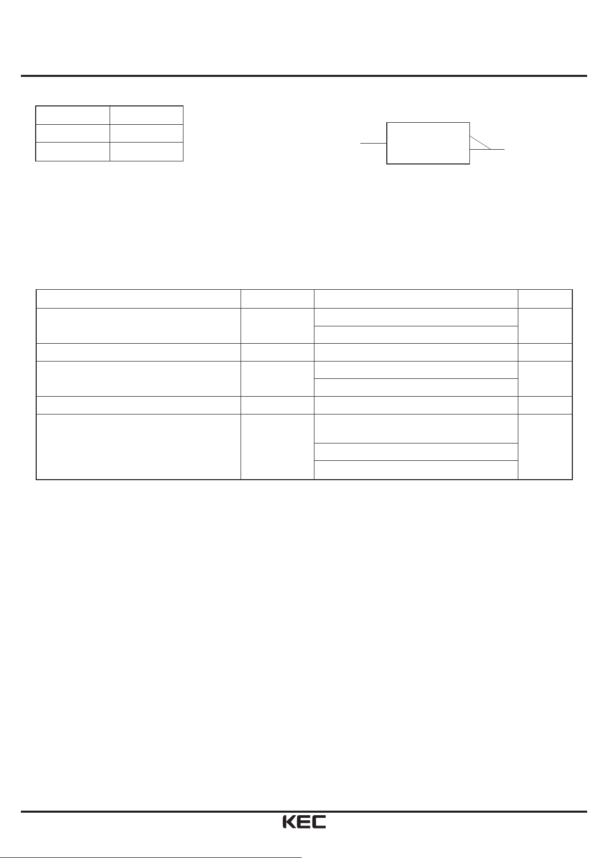
Triple Inverter
FEATURES
·High output drive : ±24mA(min.) @VCC=3V.
·Super high speed operation : tpd 2.3ns(typ.) @VCC=5V, 50pF.
·Operation voltage range : V
CC(opr)
=1.65~5.5V.
·Latch-up performance : ±500mA or more
·ESD performance : ±200V or more (EIAJ)
±2000V or more (MIL)
·Power down protection is provided on all inputs and outputs.
A
D
D
D
C
B
E
F
G
H
MAXIMUM RATINGS (Ta=25℃)
MARKING
Lot No.
Z04
Type Name
CHARACTERISTIC SYMBOL RATING UNIT
Power Supply Voltage
V
CC
-0.5~6 V
DC Input Voltage
V
IN
-0.5~6 V
DC Output Voltage
V
OUT
-0.5~6 V
Input Diode Current
I
IK
-20 mA
Output Diode Current
I
OK
-20 mA
DC Output Current
I
OUT
±50
mA
DC VCC/ground Current I
CC
±50
mA
Power Dissipation
P
D
200 mW
Storage Temperature Range
T
stg
-65~150
℃
Lead Temperature (10s)
T
L
260
℃
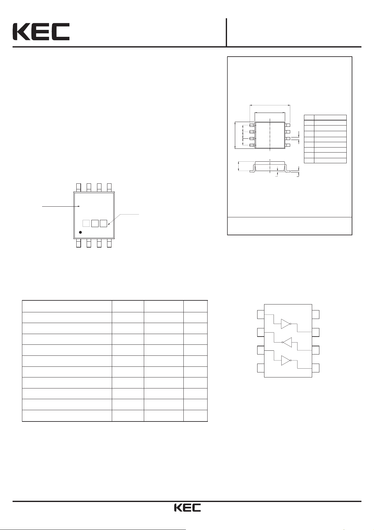
PIN CONNECTION(TOP VIEW)
1
2
3
4
1Y
3A
2Y
8
7
6
5
V
CC
1A
3Y
2A
GND
TECHNICAL DATA
OR
DIMMILLIMETERS
1
45
A
8
B
C
D
E
F
G
H
_
+
2.0 0.1
_
+
3.1 0.1
_
+
2.3 0.1
0.5
0.2+0.05/-0.04
_
0.7 0.1
+
_
0.12 0.04
+
0 ~ 0.1
US8
2002. 5. 13 1/3
KIC7WZ04FK
Truth Table
A Y
L H
H L
Logic Diagram
IN A
1
OUT Y
Recommended Operating Conditions
CHARACTERISTIC SYMBOL RATING UNIT
Supply Voltage
V
CC
1.65~5.5
V
1.5~5.5 (Note1)
Input Voltage
V
IN
0~5.5 V
Output Voltage
V
OUT
0~5.5 (Note2)
V
0~V
CC
(Note3)
Operating Temperature
T
opr
-40~85
℃
Input Rise and Fall Time
dt/d
v
0~20 (VCC=1.8V±0.15V,
2.5V±0.2V)
ns/V
0~10 (VCC=3.3V±0.3V)
0~5 (VCC=5.5V±0.5V)
Note1 : Data retention only.
Note2 : VCC=0V.
Note3 : High or low state
2002. 5. 13 2/3
Revision No : 2
 Loading...