

2006. 4. 13 1/6
SEMICONDUCTOR
TECHNICAL DATA
KIB3401F
BICD LINEAR INTEGRATED CIRCUIT
Revision No : 3
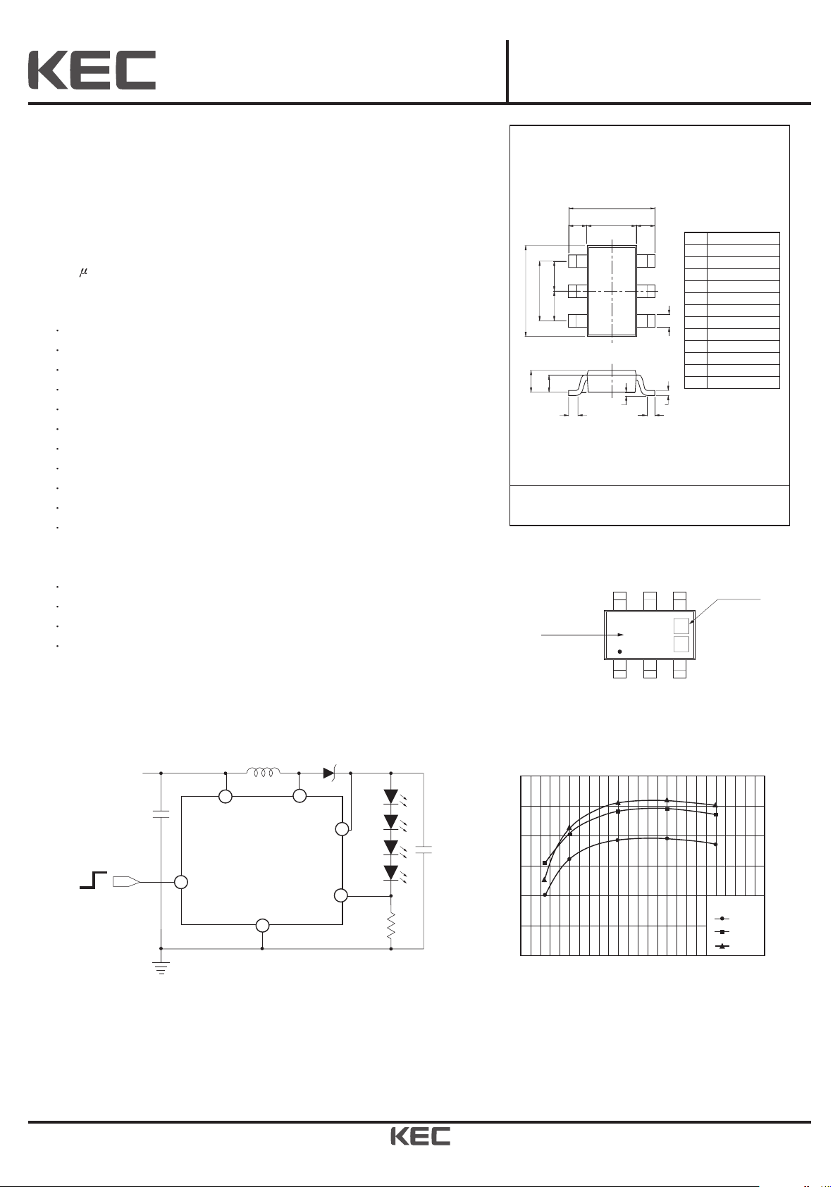
White LED Step-Up Converter
The KIB3401F is a monolithic step-up DC/DC converter specifically
designed to drive white LEDs with a constant current from Li-ion cell.
Relative large 320mV feedback voltage & it’s high accuracy help you
setting LED current with a external resistor.
KIB3401F is available in a extremely low profile & small TS-6 package.
A 10 H inductor is sufficient for most application.
FEATURES
Inherently Matched LED Current.
High Efficiency : 85% (max.)
Built in a open circuits protection for the LEDs fail.
Drives Up to four LEDs without external zener diode.
Drives Up to six LEDs with external zener diode.
Built in a N-channel MOSFET Switch.
Fast 1.1MHz(typ.) Switching Frequency.
Uses Tiny 1mm Tall Inductors.
Bulit in Thermal protection.
Wide Dimming control range : 25%~100%.
Extremely low height & small Packaging.
APPLICATIONS
Celluars Phones
PDAs
Digital Cameras
MP3 Players, Color Displays
DIM MILLIMETERS
A
B
D
E
TS6
2.9 0.2
1.6+0.2/-0.1
0.70 0.05
0.4 0.1
2.8+0.2/-0.3
1.9 0.2
0.95
0.16 0.05
0.00-0.10
0.25+0.25/-0.15
C
F
G
H
I
J
K 0.60
L 0.55
A
F
G
G
D
K
K
B
E
C
L
H
J
J
I
2
3
5
16
4
+
_
+
_
+
_
+
_
+
_
Figure1. 4Series White LED Driver in Thin TS6
0
C1, C2 : X5R OR X7R DIELECTRIC
D1 : KEC KDR730E/KDR720E (Low V )
L1 : MURATA LQH32CN100K53L OR EQUIVALENT
GND
SW
L1
C1
ON
Shutdown and
Dimming control
OFF
C2
21.5Ω
R1
KIB3401F
D1
CTL
FB
F
OVD
LED1
LED2
LED3
LED4
LOAD CURRENT (mA)
10
CONVERSION EFFICIENCY
EFFICIENCY (%)
75.00
77.00
79.00
81.00
83.00
85.00
87.00
05 2015 25
3.0V
Vin
3.6V
4.3V
1
2
4
3
6
5
V
CC
4.7 H~10 H
µ
µ
1 F
µ
V
IN
1 F
µ
TYPICAL APPLICATION
Marking
Lot No.
Type Name
401
123
654
2006. 4. 13 2/6
KIB3401F
Revision No : 3
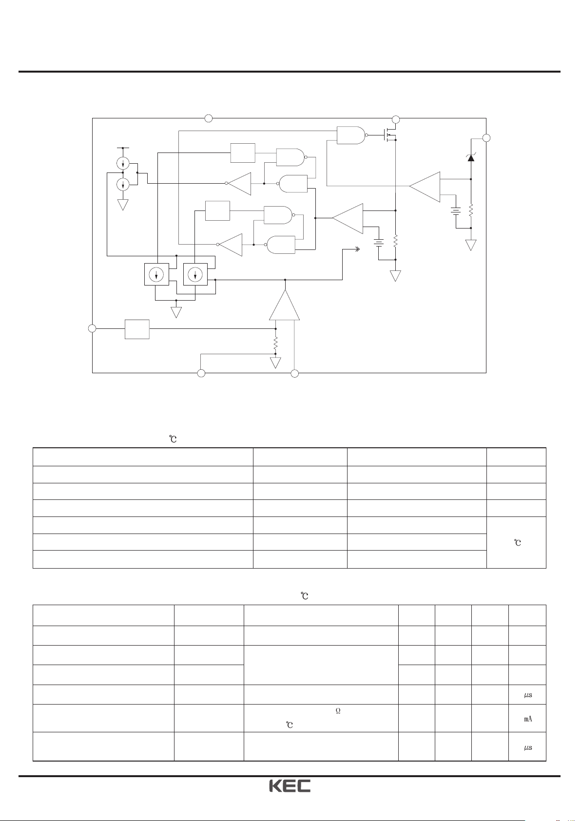
CHARATERISTICS SYMBOL RATING UNIT
Input Voltage
V
CC
-0.3 ~ 6.0 V
Switching pin Voltage
V
SW
-0.3 ~ 22 V
OVD pin Voltage
V
OVD
-0.3 ~ 22 V
Operating temperature range Topr -40 ~ 85
Storage temperature range Tstg -40 ~ 150
Maximum Junction temperature Tj 150
CHARATERISTICS SYMBOL CONDITION MIN. TYP. MAX. UNIT
Input Voltage
V
CC
- 2.8 - 5.5 V
CTL pin voltage for full LED current
V
CTL
H
VCC=3.0V
2.7 - - V
CTL pin voltage to shutdown chip
V
CTL
L
- - 0.5 V
CTL pin input pulse width
t
PW(CTL)
Both Positive and Negative pulse 33 - -
LED Current IF
VCC=3.6V, R
SENSE
=16 ,
Topr =25
, Four LED
- 20 -
CTL Response Delay
(When Power ON.)
TpdCTL
- 2 - -
MAXIMUM RATINGS (Ta=25 )
RECOMMENDED OPERATING CONDITIONS (T
opr
=-40~85 )
One Shot
One Shot
SW
OUT
OUT
OVD
VRef
Vth
320mV
FB(Rsense)
GND
CTL
ADC
+
-
OUT
+
-
+
-
+
_
+
-
+
_
+
-
+
-
+
-
2
3
6
4
1
5
V
CC
BLOCK DIAGRAM
figure 2. KIB3401F Block Diagram

2006. 4. 13 3/6
KIB3401F
Revision No : 3
ELECTRICAL CHARACTERISTIC
(Topr=-40~85
, VCC=2.8~5.5V, R
SENSE
=16 , unless otherwise noted.)
CHARATERISTICS SYMBOL CONDITION MIN. TYP. MAX. UNIT
Input Voltage
V
CC
- 2.8 - 5.5 V
Supply Current
I
CC
VCC= 3.6V, V
CTL
=3.6V
- 0.9 1.5
V
CTL
= 0V
- 0.5 1
Feedback Voltage
V
FB
VCC=V
CTL
=3.0V, T
opr
= 25 , L =10 H
294 320 346
CTL Pin Bias Current
I
CTL
VCC= 3.0V, V
CTL
= 3.0V
- 20 -
Switching Frequency
f
OSC
V
CTL
= 3.0V
0.77 1.1 1.43
Switching Pin Current
I
O(SW)
- 400 -
Switch RDS(ON)
R
ON
I
O(SW)
400
- 0.7 1.5
Switch Leak Current
I
OZ(SW)
- - 0.5 1
OVD Pin Voltage
V
OVD
- 16 20 22 V
OVD Pin Leak Current
I
OZ(OVD)
- - 0.5 1
Thermal Shutdown TSD - - 150 180
Switching Pin OVP
V
O(SW)
- 25 - - V
CTL pin voltage for Full LED Current
V
CTL H
VCC= 3.0V
2.7 - - V
CTL pin voltage to shutdown Chip
V
CTL L
- - 0.5 V
Feedback Bias Current
I
FB
- - 0.5 1
Maximum Duty Cycle
D
max
- 85 90 - %
NO. SYMBOL FUNCTION AND CONNECTION.
1 CTL
Control pin : Shutdown or dimming control. Connect external enable or dimming circuits.
Shutdown mode (IF = 0) : V
CTL
<1.0V
Dimming control mode : (IF = 20% ~ 100%, depend on V
CTL
)
1.0V < V
CTL
< 2.5V, when V
CTL
is above 2.5V IF keep its maximum value(100%).
Filtered PWM signal, above 33us of pulse width, can be used for dimming control.
2 OVD Over output voltage detect pin. Connect cathode of schottky diode and anode of highest LED.
3 SW Switch pin. Connect inductor/diode here. Minimize trace area at this pin to reduce EMI.
4 FB Feedback pin. Reference voltage is 320mV. Connect cathode of lowest LED and resistor here.
5 GND Ground pin. Connect directly to local ground plane,
6
V
CC
Input supply pin. Must be locally bypassed.
PIN FUNCTIONS

2006. 4. 13 4/6
KIB3401F
Revision No : 3
APPLICATION INFORMATION
Inductor Selection
A 10
H inductor is sufficient for most application. The efficiency
comprison of different value inductors help you design your
application circuits.
Capacitor Selection
A 1
input capacitor and output capacitor above 1 are
sufficient for most KIB3401F application.
Diode Selection
For Diode Selection, both forward voltage drop and diode
capacitance need to be considered. Shottky diodes with higher
current ratings usually have lower forward voltage and larger diode
capacitance, which can cause significant switching losses. A
schottky diode rated at 100
to 200 is sufficient for most
KIB3401F applications.
Table 1. Recommended Schottky Diodes
LED Current Control
The LED current is controlled by the feedback resistor(RSENSE
in Figure 1). The feedback reference is 320
.
The LED current is 320
/R
SENSE
. The tolerance of LED Current is
depends on tolerance of R
SENSE
and feedback reference.
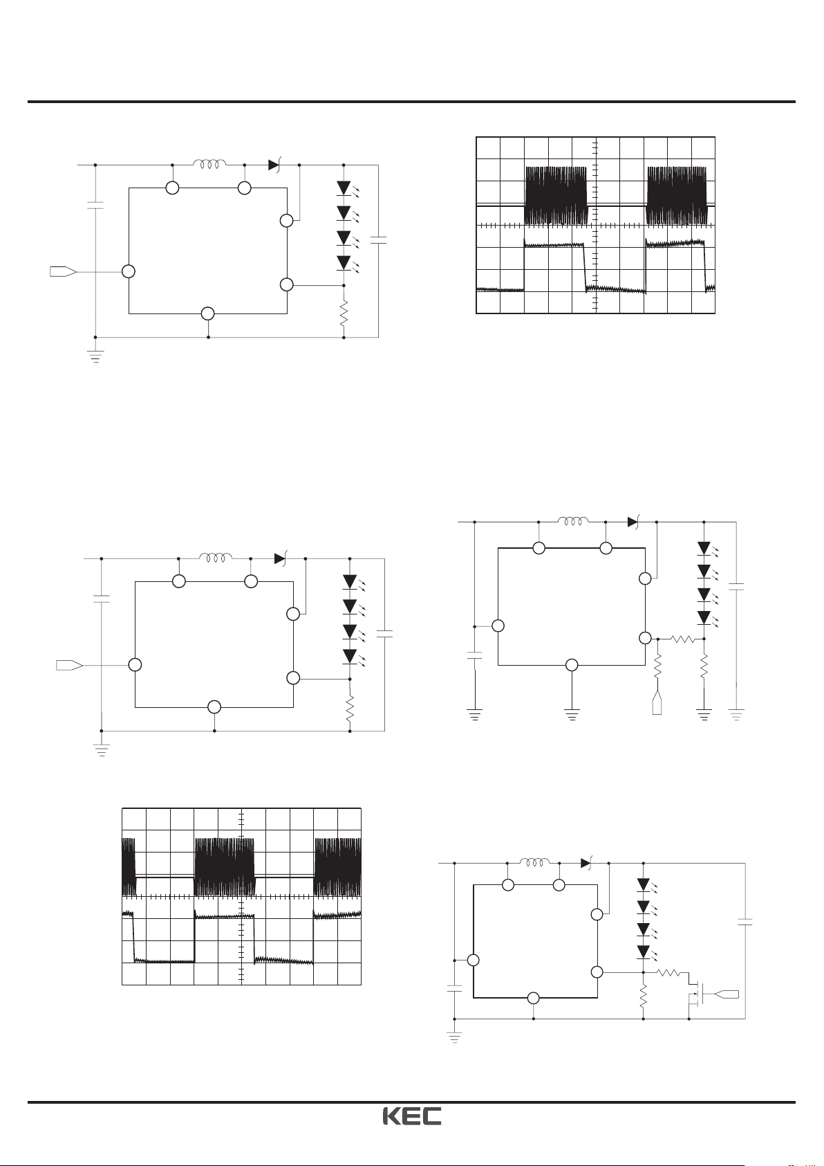
Open-Circuits Protection
In the case of output open circuit, when LEDs are disconnected
from the circuit or the LEDs fail, the feedback voltage will be zero.
The KIB3041F will then switch at a high duty cycle resulting in a
high output voltage, but Internal Over Voltage Protection Circuits
prevent output voltage ascending over OVD pin voltage( 16V ~ 22V
see Fig.4 ). This circuits is valid when driving up to 4 LEDs in
series. But, when driving more than 4 LEDs in series, Normal
output voltage could be over OVD pin voltage.
In this case, zener diode can be used to limit output voltage, but
check connection of OVD pin to VCC.(see Fig.5)
LOAD CURRENT (mA)
10
EFFICIENCY (%)
70.00
72.00
74.00
76.00
78.00
80.00
82.00
84.00
86.00
88.00
90.00
05 2015 25
4.7uH
Vin=3.6V, 4LED
Inductor=Murata
10uH
Figure3. Efficiency Comaprison of different value inductors
Figure4. 4LEDs driver with Open-circuit protection.
Figure5. 6LEDs driver with Open-circuit protection.
0
GND
SW
DZ
L1
C1
C2
21.5Ω
SENSE
R
KIB3401F
D1
CTL
FB
OVD
LED1
LED2
LED3
LED4
0
GND
SW
L1
C1
C2
16Ω
R1
KIB3401F
D1
CTL
FB
LED1
LED2
LED5
LED6
LED3
LED4
OVD
1
2
4
3
6
5
1
2
4
3
6
5
V
CC
V
CC
1 F
µ
4.7 H~10 H
µ
µ
4.7 H~10 H
µ
µ
1 F
µ
1 F
µ
1 F
µ
V
IN
V
IN
Dimming Control
There are 4 different type of dimming control circuits:
1. Using a DC Voltage to CTL pin.
Table 2 CTL pin Voltage vs I
LED
Description
V
CTL
UNIT
0V~0.5V 1V~2.5V
V
CTL
>2.5V
Rate Of the LED Current 0 25 ~ 100 100 %
Example : R
SENSE
= 16
0 5 ~ 20 20 mA
Part No.
Reverse
Voltage (V)
Forward
Current (mA)
Voltage
Drop (V)
Package
KDR730E 30 200 mA
0.6V (max)
at 200 mA
1.60
1.20
0.80
0.30
1
2
KDR720E 30 200 mA
0.5V(max)
at 200 mA
1.60
1.20
0.80
0.30
1
2
KDR412 20 500 mA
0.5V(max)
at 500 mA
0.30
1.25
1.70
2.50
2006. 4. 13 5/6
KIB3401F
Revision No : 3
2. Using a PWM Signal to CTL pin.
With the PWM signal applied to the CTL pin, the KIB3401F is turned
on or off by the signal. Typical frequency range of the PWM signal is
15kHz to 30kHz. The switching waveforms of the CTL pin PWM
control are shown in Figure 7(A) and 7(B)
Figure 7. Using a PWM Signal to CTL pin.
3. Using a DC Voltage to FB pin.
The dimming control using a DC control voltage to FB pin of the
KIB3401F is shown in Figure. The LED current can be varied
applying a DC voltage to the FB pin. The voltage can come from a
filtered PWM signal. It can be used to replace the variable DC
Voltage source in dimming control.
4. Using a Logic Signal to FB pin.
For applications that need to adjust the LED current in discret steps,
a logic signal can be used as shown in Figure 9.
Figure6. Using a DC Signal to CTL pin.
0
GND
SW
L1
C1
C2
21.5Ω
R
SENSE
KIB3401F
D1
DC
CTL
FB
OVD
LED1
LED2
LED3
LED4
1
2
4
3
6
5
V
CC
1 F
µ
4.7 H~10 H
µ
µ
1 F
µ
V
IN
0
GND
SW
L1
C1
C2
21.5Ω
R
SENSE
V
IN
KIB3401F
D1
PWM
CTL
FB
OVD
LED1
LED2
LED3
LED4
1
2
4
3
6
5
V
CC
1 F
µ
4.7 H~10 H
µ
µ
1 F
µ
V
SW
5V/Div
V
CTL
5V/Div
(A) 1kHz (2ms/Div)
0
Figure8. Using DC Voltage to FB pin.
0
GND
SW
L1
C1
C2
R1
R2
KIB3401F
D1
CTL
FB
SENSE
R
DC
OVD
LED1
LED2
LED3
LED4
0
0
1
2
4
3
6
5
V
CC
1 F
µ
1 F
µ
V
IN
0
Figure9. Using a Logic Signal to FB pin.
GND
V
CC
SW
L1
1uF
C1
1uF
C2
dim
R
LOGIC
KTK5132V
KIB3401F
D1
CTL
FB
R
SENSE
OVD
LED1
LED2
LED3
LED4
1
2
4
3
6
5
V
IN

2006. 4. 13 6/6
KIB3401F
Revision No : 3
V (V)
01234
0
V (mV)
FB
400
300
200
100
0
Icc (µA)
-10 1107030-50
TEMP ( C)
Quiescent Current vs Temperature Thermal Shut Down
V vs V
FB
FB
CTL
CTL
300
50
350
200
250
100
150
5
-60 -10 40 90
EFFICICNCY (%)
50
55
60
65
70
75
80
85
90
95
140
500
Temperature ( C)
Efficicncy vs Temperature
Vcc (V)
1.5 2.5 3.5 4.5 5.5
FREQUENCY (MHz)
SWITCHING FREQUENCY (MHz)
Frequency vs Vcc
0.91
0.92
0.93
0.94
0.95
0.96
0.97
0.98
0.99
1.00
1.01
6.5
-50 0 50
0
0.2
0.4
0.6
0.8
1.0
1.2
1.4
1.6
1.8
100
Temperature ( C)
Switching Frequency vs Temperature
TEMP ( C)
350
300
0
V (mV)
FB
125 185175165145115 155135105
400
200
150
100
50
250
Vin=3.0V
Vin=3.6V
Vin=4.3V
V
f
V
in=
2.7V
Vin=3.6V
Vin=4.3V
 Loading...